JP6665994B2 - Electronic display module and device using the same - Google Patents
Electronic display module and device using the sameDownload PDFInfo
- Publication number
- JP6665994B2 JP6665994B2JP2015216251AJP2015216251AJP6665994B2JP 6665994 B2JP6665994 B2JP 6665994B2JP 2015216251 AJP2015216251 AJP 2015216251AJP 2015216251 AJP2015216251 AJP 2015216251AJP 6665994 B2JP6665994 B2JP 6665994B2
- Authority
- JP
- Japan
- Prior art keywords
- circuit board
- display module
- electronic display
- substrate
- module according
- Prior art date
- Legal status (The legal status is an assumption and is not a legal conclusion. Google has not performed a legal analysis and makes no representation as to the accuracy of the status listed.)
- Active
Links
Images


Classifications
- G—PHYSICS
- G06—COMPUTING OR CALCULATING; COUNTING
- G06F—ELECTRIC DIGITAL DATA PROCESSING
- G06F3/00—Input arrangements for transferring data to be processed into a form capable of being handled by the computer; Output arrangements for transferring data from processing unit to output unit, e.g. interface arrangements
- G06F3/01—Input arrangements or combined input and output arrangements for interaction between user and computer
- G06F3/03—Arrangements for converting the position or the displacement of a member into a coded form
- G06F3/041—Digitisers, e.g. for touch screens or touch pads, characterised by the transducing means
- G—PHYSICS
- G04—HOROLOGY
- G04G—ELECTRONIC TIME-PIECES
- G04G17/00—Structural details; Housings
- G04G17/02—Component assemblies
- G04G17/04—Mounting of electronic components
- G—PHYSICS
- G04—HOROLOGY
- G04G—ELECTRONIC TIME-PIECES
- G04G17/00—Structural details; Housings
- G04G17/02—Component assemblies
- G04G17/06—Electric connectors, e.g. conductive elastomers
- G—PHYSICS
- G04—HOROLOGY
- G04G—ELECTRONIC TIME-PIECES
- G04G21/00—Input or output devices integrated in time-pieces
- G04G21/08—Touch switches specially adapted for time-pieces
- G—PHYSICS
- G06—COMPUTING OR CALCULATING; COUNTING
- G06F—ELECTRIC DIGITAL DATA PROCESSING
- G06F1/00—Details not covered by groups G06F3/00 - G06F13/00 and G06F21/00
- G06F1/16—Constructional details or arrangements
- G06F1/1613—Constructional details or arrangements for portable computers
- G06F1/163—Wearable computers, e.g. on a belt
- G—PHYSICS
- G06—COMPUTING OR CALCULATING; COUNTING
- G06F—ELECTRIC DIGITAL DATA PROCESSING
- G06F3/00—Input arrangements for transferring data to be processed into a form capable of being handled by the computer; Output arrangements for transferring data from processing unit to output unit, e.g. interface arrangements
- G06F3/01—Input arrangements or combined input and output arrangements for interaction between user and computer
- G06F3/03—Arrangements for converting the position or the displacement of a member into a coded form
- G06F3/041—Digitisers, e.g. for touch screens or touch pads, characterised by the transducing means
- G06F3/0416—Control or interface arrangements specially adapted for digitisers
- G06F3/04164—Connections between sensors and controllers, e.g. routing lines between electrodes and connection pads
Landscapes
- Engineering & Computer Science (AREA)
- Physics & Mathematics (AREA)
- General Physics & Mathematics (AREA)
- Theoretical Computer Science (AREA)
- General Engineering & Computer Science (AREA)
- Human Computer Interaction (AREA)
- Computer Hardware Design (AREA)
- Devices For Indicating Variable Information By Combining Individual Elements (AREA)
- Computer Networks & Wireless Communication (AREA)
- Liquid Crystal (AREA)
- Nonlinear Science (AREA)
- Mathematical Physics (AREA)
- Chemical & Material Sciences (AREA)
- Crystallography & Structural Chemistry (AREA)
- Optics & Photonics (AREA)
- Electroluminescent Light Sources (AREA)
Description
Translated fromJapanese本発明は、電子装置とその素子に関するものであって、特に、電子ディスプレイモジュールとそのディスプレイパネルに関するものである。 The present invention relates to an electronic device and its elements, and more particularly, to an electronic display module and its display panel.
電子ディスプレイモジュールは、電気信号を可視画像に転換して、人間が、電気信号中に含まれる情報を知ることができるようにすることができる光電子デバイス(optoelectronic device)である。タッチセンシング機能を有する電子ディスプレイモジュールに対する要求は、近年、増加している。特に、タッチセンシング機能を、電子ディスプレイモジュールに統合する電子装置、たとえば、携帯電話、PDA、タブレット型コンピュータは、操作がやりやすいので、どんどん普及しており、これらの装置は、“タッチディスプレイパネル”と称される。各種タッチディスプレイパネルが発展し、たとえば、アウトセル型(out-cell type)タッチディスプレイパネル、インセル型(in-cell type)タッチディスプレイパネル、および、オンセル型(on-cell type)タッチディスプレイパネルがある。 Electronic display modules are optoelectronic devices that can convert an electrical signal into a visible image so that a human can know the information contained in the electrical signal. The demand for an electronic display module having a touch sensing function has been increasing in recent years. In particular, electronic devices that integrate touch sensing functions into electronic display modules, such as mobile phones, PDAs, and tablet computers, are becoming more and more popular because they are easy to operate, and these devices are known as “touch display panels”. It is called. Various types of touch display panels have been developed, for example, an out-cell type touch display panel, an in-cell type touch display panel, and an on-cell type touch display panel.
ユーザーは、指、タッチペン、または、その他を用いて、アクティブ領域をタッチすることにより、タッチディスプレイパネル上で、各種機能を実行することができる。一般に、アクティブ領域は、タッチセンサー式(touch-sensitive)ではない不透明の周辺領域により囲まれる。タッチディスプレイパネルを用いた装置の所定サイズに対し、周辺領域のサイズは、ユーザーにとって使用可能なアクティブ領域を制限するので、周辺領域を縮小して、アクティブ領域の割合を増加させることが望まれる。 The user can execute various functions on the touch display panel by touching the active area with a finger, a touch pen, or the like. Generally, the active area is surrounded by an opaque peripheral area that is not touch-sensitive. For a given size of a device using a touch display panel, the size of the peripheral area limits the active area available to the user, so it is desirable to reduce the peripheral area and increase the proportion of the active area.
革新的構造を有する電子ディスプレイモジュールと電子装置を提供することを目的とする。 An object of the present invention is to provide an electronic display module and an electronic device having an innovative structure.
本発明のいくつかの実施態様によると、電子ディスプレイモジュールは、タッチディスプレイアセンブリ、第一回路板、および、第二回路板を有する。タッチディスプレイアセンブリは、主基板、および、カバー基板を有する。主基板は、アクティブ領域、および、第一方向で、外に延伸する第一延伸領域を有する。カバー基板は、第二方向で外に延伸する第二延伸領域を有する。第一回路板は第一延伸領域に接続される。第二回路板は第二延伸領域に接続される。第一方向のアクティブ領域の辺縁から第一延伸領域の辺縁までの投射距離は、第二方向のアクティブ領域の辺縁から第二延伸領域の辺縁までの投射距離より大きい。 According to some embodiments of the present invention, an electronic display module has a touch display assembly, a first circuit board, and a second circuit board. The touch display assembly has a main substrate and a cover substrate. The main substrate has an active region and a first extension region extending outward in a first direction. The cover substrate has a second stretched region extending outward in a second direction. The first circuit board is connected to the first extension area. The second circuit board is connected to the second extension area. The projection distance from the edge of the active area in the first direction to the edge of the first extension area is larger than the projection distance from the edge of the active area in the second direction to the edge of the second extension area.
いくつかの実施態様において、タッチディスプレイアセンブリは、複数のトランジスタ、シーリング材、および、液晶層を有する。トランジスタは、主基板のアクティブ領域上に形成される。シーリング材が、主基板とカバー基板間に設置される。液晶層は、主基板とカバー基板との間に、且つ、シーリング材に隣接して設置される。 In some embodiments, the touch display assembly has a plurality of transistors, a sealant, and a liquid crystal layer. The transistor is formed on an active area of the main substrate. A sealing material is provided between the main substrate and the cover substrate. The liquid crystal layer is provided between the main substrate and the cover substrate and adjacent to the sealing material.
いくつかの実施態様において、第一延伸領域は、カバー基板により露出する。 In some embodiments, the first extension region is exposed by the cover substrate.
いくつかの実施態様において、第一回路板の長さは、第二回路板の長さより長い。 In some embodiments, the length of the first circuit board is longer than the length of the second circuit board.
いくつかの実施態様において、第一方向は第二方向と反対である。 In some embodiments, the first direction is opposite to the second direction.
いくつかの実施態様において、電子ディスプレイモジュールは、さらに、保護基板とタッチセンシングユニットを有する。カバー基板は、主基板と保護基板間に設置される。タッチセンシングユニットは、カバー基板と保護基板間に設置される。 In some embodiments, the electronic display module further has a protection substrate and a touch sensing unit. The cover substrate is provided between the main substrate and the protection substrate. The touch sensing unit is installed between the cover substrate and the protection substrate.
いくつかの実施態様において、電子ディスプレイモジュールは、さらに、主基板上に設置される第一駆動チップ、および、第二回路板上に設置される第二駆動チップを有する。 In some embodiments, the electronic display module further has a first drive chip located on the main substrate and a second drive chip located on the second circuit board.
いくつかの実施態様において、タッチディスプレイアセンブリは、複数のトランジスタ、シーリング材、および、OLED層を有する。トランジスタは、主基板のアクティブ領域上に形成される。シーリング材は、主基板とカバー基板間に設置される。OLED層は、主基板とカバー基板との間に、且つ、シーリング材に隣接して設置される。 In some embodiments, the touch display assembly has a plurality of transistors, a sealant, and an OLED layer. The transistor is formed on an active area of the main substrate. The sealing material is provided between the main substrate and the cover substrate. The OLED layer is provided between the main substrate and the cover substrate and adjacent to the sealing material.
いくつかの実施態様において、電子ディスプレイモジュールは、さらに、バックライトアセンブリと第三回路板を有する。バックライトアセンブリは、タッチディスプレイアセンブリに隣接するように配置されると共に、バックライトを、タッチディスプレイアセンブリに提供するように設定される。第三回路板は、バックライトアセンブリに電気的に接続される。第一回路板は第三回路板と重なり、且つ、第一回路板は、第三回路板を部分的に露出するスルーホールを有する。導電材が、スルーホール中に配置されると共に、第三回路板を第一回路板に電気的に接続する。 In some embodiments, the electronic display module further has a backlight assembly and a third circuit board. The backlight assembly is positioned adjacent to the touch display assembly and is configured to provide backlight to the touch display assembly. The third circuit board is electrically connected to the backlight assembly. The first circuit board overlaps the third circuit board, and the first circuit board has a through hole that partially exposes the third circuit board. A conductive material is disposed in the through hole and electrically connects the third circuit board to the first circuit board.
いくつかの実施態様において、電子ディスプレイモジュールは、さらに、バックライトアセンブリと第三回路板を有する。バックライトアセンブリは、タッチディスプレイアセンブリに隣接ように配置されると共に、バックライトをタッチディスプレイアセンブリに提供するように設定される。第三回路板は、バックライトアセンブリに電気的に接続される。第三回路板は、第一回路板により被覆される第一部分、および、第一回路板により被覆される第二部分を有する。第三回路板は、第二部分により、第一回路板に電気的に接続される。 In some embodiments, the electronic display module further has a backlight assembly and a third circuit board. The backlight assembly is positioned adjacent to the touch display assembly and is configured to provide backlight to the touch display assembly. The third circuit board is electrically connected to the backlight assembly. The third circuit board has a first portion covered by the first circuit board and a second portion covered by the first circuit board. The third circuit board is electrically connected to the first circuit board by the second portion.
本発明のいくつかの実施態様によると、電子装置は、上述のいずれかの実施態様の円形のハウジングとタッチディスプレイアセンブリを有する。底縁は、第一距離で、タッチディスプレイアセンブリの実質的中心から離れ、上端は、第二距離で、タッチディスプレイアセンブリの実質的中心から離れ、且つ、第一距離は第二距離より大きいが、ハウジングの半径より小さい。このほか、底縁と上端は、互いに平行な直線である。 According to some embodiments of the present invention, an electronic device has the circular housing and touch display assembly of any of the embodiments described above. The bottom edge is away from the substantial center of the touch display assembly at a first distance, the top edge is away from the substantial center of the touch display assembly at a second distance, and the first distance is greater than the second distance, Smaller than the radius of the housing. In addition, the bottom edge and the upper end are straight lines parallel to each other.
本発明により、アクティブ領域の割合を増加させることができる。 According to the present invention, the ratio of the active area can be increased.
上記及び他の目的及び本発明の特徴は、添付図面とともに以下の記載を参照することにより明らかとなる。 The above and other objects and features of the present invention will become apparent by referring to the following description in conjunction with the accompanying drawings.
本発明の電子ディスプレイモジュール、および、電子装置は、以下で詳細に説明する。以下の詳細な説明において、説明の目的のため、多くの特定の詳細と実施態様が示されて、本発明の十分な理解を提供する。以下の詳細な説明において、特定の素子と配置が示されて、本発明をよりはっきりと記述する。しかし、ここで示される実施態様は説明を目的とするものであり、発明概念が各種方式で具体化され、それらの実施態様に限定するものではないことが理解できる。このほか、異なる実施態様の図面は、類似の、および/または、対応する数字を用いて、類似の、および/または、対応する素子を示し、本発明をはっきりと記述する。しかし、異なる実施態様の図面において、類似の、および/または、対応する数字の使用は、異なる実施態様間の相互関係を意味するのではない。このほか、この明細書において、たとえば、"第二材料層上に設置された第一絶縁バンプ"という表現は、第一絶縁バンプと第二材料層の直接接触だけを示すのではなく、第一絶縁バンプと第二材料層間にひとつ以上の中間層がある非接触状態のことも意味する。上述のような状況下で、第一絶縁バンプは、第二材料層に直接接触しない。 The electronic display module and the electronic device according to the present invention will be described in detail below. In the following detailed description, for purposes of explanation, numerous specific details and embodiments are set forth in order to provide a thorough understanding of the present invention. In the following detailed description, specific elements and arrangements are shown to more clearly describe the invention. However, it will be understood that the embodiments shown herein are for illustrative purposes, and that the inventive concepts may be embodied in various ways and are not limited to those embodiments. In addition, figures of different embodiments use similar and / or corresponding numerals to indicate similar and / or corresponding elements, and to clearly describe the invention. However, the use of similar and / or corresponding numerals in the drawings of different embodiments does not imply a correlation between the different embodiments. In addition, in this specification, for example, the expression "the first insulating bump provided on the second material layer" does not indicate only the direct contact between the first insulating bump and the second material layer, but the first insulating bump. It also means a non-contact state in which there is one or more intermediate layers between the insulating bump and the second material layer. Under the circumstances described above, the first insulating bump does not directly contact the second material layer.
注意すべきことは、本発明の図面における素子、または、装置は、当業者に知られた形式、または、配置で現されることである。このほか、"一層がもうひとつの層上にある"、"一層がもうひとつの層上に設置される"という表現は、その層が直接、もうひとつの層に接触することを示すだけでなく、その層が、直接、もうひとつの層と接触せず、層ともう一層間のひとつ以上の中間層がある場合もある。 It should be noted that the elements or devices in the drawings of the present invention may be embodied in a form or arrangement known to those skilled in the art. In addition, the expressions "one layer is on another layer" and "one layer is placed on another layer" not only indicate that the layer directly contacts another layer, In some cases, the layer does not directly contact another layer and there is one or more intermediate layers between the layer and another.
このほか、この明細書において、相対表現が用いられる。たとえば、“下”、“底部”、“高い”や“頂部”が用いられて、素子間の位置を説明する。一装置が逆さまに反転する場合、“下”側の一素子は“上”側の素子になることが理解できる。 In addition, in this specification, a relative expression is used. For example, "bottom", "bottom", "high" and "top" are used to describe the location between elements. It can be seen that if one device is inverted upside down, one element on the “lower” side will be the element on the “upper” side.
“約”と“ほぼ”という用語は、一般的には、表示値の+/-20%、さらに、一般的には、表示値の+/-10%、さらに、一般的には、表示値の+/-5%である。本発明の表示値は概略値である。特に記述がなければ、表示値は、“約”や“ほぼ”の意味を含んでいる。 The terms "about" and "approximately" are generally used to mean +/- 20% of the stated value, more generally +/- 10% of the stated value, and more generally +/- 5%. The display values of the present invention are approximate values. Unless otherwise specified, the displayed value includes the meaning of “about” or “almost”.
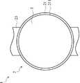
図1を参照すると、いくつかの実施態様において、電子装置1は、ウェアラブル装置で、たとえば、タッチセンシング機能がある腕時計である。電子装置1は、ハウジング2、および、電子ディスプレイモジュール3を有する。ハウジング2は、本体210、および、着用者が電子装置1を本体の適当な位置に固定することができる固定素子230を有する。本体210は、ハウジングの上表面に、開口部211を有する収容空間を定義し、且つ、開口部211は、円形の縁を有する。電子ディスプレイモジュール3は、開口部211に相対する本体210上に設置される。 Referring to FIG. 1, in some embodiments, the electronic device 1 is a wearable device, for example, a wristwatch having a touch sensing function. The electronic device 1 has a housing 2 and an
図2〜図4を参照すると、図2は、電子ディスプレイモジュール3の概略図、図3は、図2のA−A´に沿った断面図、図4は、図2のB−B´に沿った断面図である。いくつかの実施態様において、電子ディスプレイモジュール3は、タッチディスプレイアセンブリ4、第一回路板5、第二回路板6、第一駆動チップ55、第二駆動チップ65(図4)、バックライトモジュール7(図3)、および、保護基板8(図3)を有する。電子ディスプレイモジュール3の素子は、追加、または、省略でき、本発明は、実施態様に制限されない。 Referring to FIGS. 2 to 4, FIG. 2 is a schematic diagram of the
いくつかの実施態様において、タッチディスプレイアセンブリ4は、タッチセンシング機能がある液晶ディスプレイで、且つ、主基板10、後偏光板15、前偏光板16、カバー基板20、タッチセンシング層30、および、光学素子層40(図3)を有する。いくつかの実施態様において、タッチディスプレイアセンブリ4は、主基板10、前偏光板、タッチセンシング層30、および、有機発光ダイオードデバイスアレイのような光学素子層40を有する有機発光ダイオードディスプレイ(OLED)である。 In some embodiments, the touch display assembly 4 is a liquid crystal display having a touch sensing function, and includes a
図3に示されるように、主基板10とカバー基板20は、シーリング材17により互いに間隔を隔てている。主基板10は、複数の薄膜トランジスタ(TFT)、画素、および、駆動回路を有する。この実施態様において、カバー基板20は、複数のカラーフィルター、ブラックマトリクス、および、電極を有するカラーフィルター基板である。OLEDのカバー基板20は、表示やタッチのための複数の電極パターンを有するカバー基板である。光学素子層40、たとえば、液晶層は、主基板10とカバー基板20間に設置される。シーリング材17は、主基板10とカバー基板20間に設置され、光学素子層40の周りに位置する。図3に示される実施態様において、主基板10の一部領域はカバー基板20により被覆され、残りの部分は、カバー基板20により被覆されない。たとえば、主基板10は、アクティブ領域AA1、周辺領域BA1、および、延伸領域EA1を有する。カバー基板20は、アクティブ領域AA1と周辺領域BA1に相対する主基板10を被覆し、延伸領域EA1を露出する。アクティブ領域AA1は、複数のTFT、画素、回路を有する。周辺領域BA1と延伸領域EA1は、アクティブ領域AA1のTFT、画素、および、回路を接続する複数の駆動回路を有する。 As shown in FIG. 3, the
いくつかの実施態様において、主基板10のアクティブ領域AA1は、カバー基板20の最外部上に形成される遮光素子25の内側辺縁251により定義される。遮光素子25は、主基板10に面するカバー基板20の内側表面上に形成される。あるいは、遮光素子25は、主基板10から離れるカバー基板20の外側表面上に形成される。アクティブ領域AA1は、中心C(図2)がある円形であるが、本発明は、これに限定されない。 In some embodiments, the active area AA <b> 1 of the
周辺領域BA1は、アクティブ領域AA1と延伸領域EA1間に位置する。駆動回路の広がる配線が、周辺領域BA1上に形成される。延伸領域EA1は、延伸領域EA1から第一方向D1で、外側に延伸すると共に、第一外縁11で終了する。第一外縁11は、第一方向D1のタッチディスプレイアセンブリ3の最外部辺縁であるので、以下の記述において、説明の目的のため、第一外縁11は、タッチディスプレイアセンブリ3の底縁と称される。 The peripheral area BA1 is located between the active area AA1 and the extension area EA1. The wiring that extends the drive circuit is formed on the peripheral area BA1. The stretching area EA1 extends outward from the stretching area EA1 in the first direction D1, and ends at the first
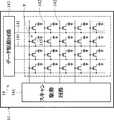
いくつかの実施態様において、主基板10は、TFTガラス基板で、且つ、タッチディスプレイアセンブリ3の各画素の光線を制御するように設置される複数の半導体トランジスタを有する。たとえば、図5に示されるように、回路ユニット14は、主基板10上に形成され、且つ、複数のデータライン141と複数のゲートライン142を有する。データライン141は、データ駆動回路143に電気的に接続され、互いに平行に延伸する。ゲートライン142は、スキャン駆動回路144に電気的に接続されると共に、互いに平行に延伸する。ゲートライン142はデータライン141と交差し、二つの隣接するゲートライン142と二つの隣接するデータライン141により構成される領域が、画素領域Pとして定義される。複数の半導体トランジスタ145が、画素領域P中に形成される。半導体トランジスタ145は、光学素子層40を制御するように設置される画素電極(図示しない)に接続される。 In some embodiments, the
図3を再度参照すると、タッチセンシング機能を提供するタッチセンシング層30が、前偏光板16とカバー基板20間に設置される。いくつかの実施態様において、タッチセンシング層30は、複数の送信電極(図示しない)と複数の受信電極(図示しない)を有するセンシングアレイを含む。水平センシング電極と垂直センシング電極間の電界の変化を検出することにより、タッチ位置が判断される。 Referring to FIG. 3 again, a
図4に示されるように、カバー基板20は、アクティブ領域AA2と延伸領域EA2を有する。いくつかの実施態様において、アクティブ領域AA2は、前偏光板16、および、アクティブ領域AA2から、第二方向D2で延伸する延伸領域EA2により被覆され、且つ、上端21で終了するカバー基板20の領域である。第二方向D2は、主基板10の延伸領域AA1が延伸する方向に沿った第一方向D1(図2)と異なる。第二外縁21は、第二方向D2のタッチディスプレイアセンブリ3の最外部辺縁であるので、以下の記述において、説明の目的のため、第二外縁21は、タッチディスプレイアセンブリ3の上端と称される。 As shown in FIG. 4, the
いくつかの実施態様において、図2に示されるように、第二方向D2は、第一方向D1と反対で、タッチディスプレイアセンブリ3の底縁11と上端21は直線、且つ、互いに平行であるが、本発明は、これに限定されない。いくつかの実施態様において、底縁11と上端21は、タッチディスプレイアセンブリ3の実質的中心Cの二つの異なる側に位置する。いくつかの実施態様において、底縁11と上端21は、タッチディスプレイアセンブリ3の実質的中心Cの二つの反対側に位置する。実質的中心Cは、アクティブ領域AA1の中心である。いくつかの実施態様において、主基板10の底縁11からアクティブ領域AA1までの第一距離Y1は、主基板10の上端21の投影からアクティブ領域AA1までの第二距離Y2と異なる。第一距離Y1は、第二距離Y2より大きい。 In some embodiments, as shown in FIG. 2, the second direction D2 is opposite to the first direction D1, and the
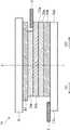
図3を参照すると、いくつかの実施態様において、バックライトモジュール7は、タッチディスプレイアセンブリ4に隣接するように配置される。バックライトモジュール7は、バックライトアセンブリ71、第三回路板72、および、後方ベゼル73を有する。バックライトアセンブリ71は、後方ベゼル73に設置されて、バックライトをタッチディスプレイアセンブリ4に提供する。第三回路板72は、バックライトアセンブリ71に接続される。第三回路板72はフレキシブルプリント回路である。第三回路板72の一部は、後方ベゼル73の後表面731に位置する。いくつかの実施態様において、保護基板8は、透明粘着シート(optical clear adhesive、OCA)81により、前偏光板16に設置されて、タッチディスプレイアセンブリ4がダメージを受けるのを保護する。 Referring to FIG. 3, in some embodiments, the
いくつかの実施態様において、図3に示されるように、第一回路板5は、タッチディスプレイアセンブリ3の底縁11に接続されると共に、主基板10に配線することにより、半導体トランジスタ145(図5)に電気的に接続される。第一回路板5はフレキシブルプリント回路である。第一回路板5の一部は、タッチディスプレイアセンブリ4の前に位置し、第一回路板5の残りの部分は、タッチディスプレイアセンブリ4の後方に位置すると共に、後方ベゼル73の後表面731に接続される。チップオンガラス(chip-on-glass、COG)技術により、第一駆動チップ55が主基板10の延伸領域EA1に位置すると共に、第一回路板5と電気的に接続される。 In some embodiments, as shown in FIG. 3, the
いくつかの実施態様において、図4に示されるように、第二回路板6は、タッチディスプレイアセンブリ3の上端21に接続されると共に、カバー基板20に配線することにより、タッチセンシング層30に電気的に接続される。第二回路板6はフレキシブルプリント回路である。第二回路板6の一部は、タッチディスプレイアセンブリ4の前に位置し、第二回路板6の残りの部分は、タッチディスプレイアセンブリ4の後ろに位置すると共に、後方ベゼル73の後表面731に接続される。第二駆動チップ65は、チップオンフレキシブルプリント回路(COF)技術により、タッチディスプレイアセンブリ3の後方に設置される第二回路板6の一部に接続される。 In some embodiments, as shown in FIG. 4, the
いくつかの実施態様において、第二回路板6と第三回路板72は、第一回路板5に電気的に接続され、第一回路板5により電気信号を受信する。第二回路板6は、第一回路板5より長い。いくつかの実施態様において、図6に示されるように、電子ディスプレイモジュール3は、さらに、タッチディスプレイアセンブリ3の後ろに位置する第一回路板5の一部に電気的に接続されるコネクタ91を有する。第二回路板6は、コネクタ91により、第一回路板5に電気的に接続される。いくつかの実施態様において、図6に示されるように、第三回路板72は、第一回路板5により被覆される第一部分721、および、第一回路板5により被覆される第二部分723を有する。第三回路板72の第二部分723は、溶接材料など、適当な導電材92により、第一回路板5に電気的に接続されているが、本発明は、これらの実施態様に限定されない。 In some embodiments, the
図7は、本発明のいくつかの実施態様による電子ディスプレイモジュール3’の概略図である。図7において、電子ディスプレイモジュール3のそれらと類似する素子は同じ符号で示され、簡略のために、その特徴は繰り返し説明しない。電子ディスプレイモジュール3’と電子ディスプレイモジュール3間の差は、第一回路板5に代わって、第一回路板5’を有することである。 FIG. 7 is a schematic diagram of an electronic display module 3 'according to some embodiments of the present invention. In FIG. 7, elements similar to those of the
いくつかの実施態様において、後方ベゼル73の後表面731に接続される第一回路板5’の一部は、ひとつ以上のスルーホール501を有する。第一回路板5’は第三回路板72と重なり、且つ、スルーホール501中に配置される、はんだ材など、適当な導電材により、第三回路板72に電気的に接続される。 In some embodiments, a portion of the first circuit board 5 'connected to the
上述の実施態様において、電子ディスプレイモジュール3は、イメージを表示するために設置される円形のアクティブ領域を有するので、電子ディスプレイモジュール3は、円形開口部211(図1)を有するハウジング2との高い互換性を有する。このほか、上述の実施態様において、第一回路板5と第二回路板6は、それぞれ、タッチディスプレイアセンブリ4の両端に位置する底縁11と上端10に接続される。よって、同一端に二回路板を有するその他のディスプレイモジュールと比較すると、電子ディスプレイモジュール3のアクティブ領域と最外部辺縁間の周辺領域の幅(すなわち、図2に示される距離Y1とY2)が減少する。その結果、電子ディスプレイモジュール3を用いた最終製品の所定サイズに対し、最終製品のアクティブ領域の割合が増加する。 In the embodiment described above, the
本発明の電子ディスプレイモジュールは、上述の実施態様に限定されない。タッチセンシング機能を提供するタッチセンシング層は、アドオン型タッチパネル(add-on type touch panel)、または、統合型タッチパネル(integrated type touch panel)に形成される。以下の記述において、電子ディスプレイモジュールのいくつかの可能な実施方法が説明される。 The electronic display module of the present invention is not limited to the embodiments described above. The touch sensing layer providing the touch sensing function is formed on an add-on type touch panel or an integrated type touch panel. In the following description, several possible implementations of the electronic display module will be described.
図8を参照すると、いくつかの実施態様によるオンセル型液晶パネルを有する電子ディスプレイモジュール3aは、主基板10a、前偏光板16a、カバー基板20a、タッチセンシング層30a、光学素子層40a、第一回路板5、第二回路板6、および、保護基板8を有する。 Referring to FIG. 8, an
いくつかの実施態様において、カバー基板20aは、主基板10aの一部を被覆する。光学素子層40aは、主基板10aとカバー基板20a間に位置する。タッチセンシング層30aは、フォトリソグラフィプロセスで、カバー基板20a上に一体化して形成される。前偏光板16aはタッチセンシング層30a上に設置される。第一回路板5は、主基板10aの底縁11a上に位置する。第二回路板6は、カバー基板20aの上端22a上に位置する。いくつかの実施態様において、上端は、第一方向D1と反対の第二方向D2で外に延伸する保護基板8の一部である。上端22aと底縁11aは、主基板10aのアクティブ領域の中心を通過する中心線Cの二つの反対側に位置する。 In some embodiments,
図9を参照すると、いくつかの実施態様によるオンセル型OLEDパネルを有する電子ディスプレイモジュール3bは、主基板10b、前偏光板16b、カプセル基板20b、タッチセンシング層30b、光学素子層40b、第一回路板5、第二回路板6、および、保護基板8を有する。 Referring to FIG. 9, an
いくつかの実施態様において、カプセル基板20b、たとえば、ガラス基板は、主基板10bの一部を被覆する。光学素子層40b、たとえば、OLED層は、主基板10bとカプセル基板20b間に設置される。タッチセンシング層30bは、フォトリソグラフィプロセスで、一体的に、カバー基板20b上に形成される。前偏光板16bはタッチセンシング層30b上に設置される。第一回路板5は、主基板10bの底縁11b上に位置する。第二回路板6は、保護基板8の上端22b上に設置(接合)される。 In some embodiments, the
図10を参照すると、いくつかの実施態様によるハイブリッドインセル型(Hybrid in-cell type)液晶パネルを有する電子ディスプレイモジュール3cは、主基板10c、前偏光板16c、カバー基板20c、第一タッチセンシング層31c、第二タッチセンシング層30c、光学素子層40c、第一回路板5、第二回路板6、および、保護基板8を有する。 Referring to FIG. 10, an
いくつかの実施態様において、カバー基板20cは、主基板10cの一部を被覆する。光学素子層40cは、主基板10cとカバー基板20c間に設置される。第一タッチセンシング層31cは、主基板10cと光学素子層40c間に位置する。第二タッチセンシング層30cは、フォトリソグラフィプロセスで、一体的に、カバー基板20c上に形成される。前偏光板16cは、第二タッチセンシング層30c上に設置される。第一回路板5は、主基板10cの底縁11c上に位置する。第二回路板6は、カバー基板20cの上端22c上に位置する。上端22cと底縁11cは、主基板10cのアクティブ領域の中心線を通過する中心線Cの二つの反対側に位置する。 In some embodiments,
図11を参照すると、いくつかの実施態様による電子ディスプレイモジュール3dは、ディスプレイパネル4d、タッチセンシング層30d、第一回路板5、第二回路板6、および、保護基板8を有する。 Referring to FIG. 11, an
いくつかの実施態様において、ディスプレイパネル4dは、主基板10d、前偏光板16d、カバー基板20d、および、光学素子層40dを有する。カバー基板20dは、主基板10dの一部を被覆する。光学素子層40d、たとえば、OLED層は、主基板10dとカバー基板20d間に設置される。第一電極層31bは、主基板10dと光学素子層40d間に位置する。第二電極層30dは、フォトリソグラフィプロセスで、一体的に、カプセル基板20d上に形成される。前偏光板16dは第二タッチセンシング層30d上に設置される。第一回路板5は、主基板10dの底縁11dに位置する。第二回路板6は、カプセル基板20dの上端22dに位置する。いくつかの実施態様において、上端は、第一方向D1と反対の第二方向D2に外に延伸する保護基板8の一部である。上端22dと底縁11dは、主基板10dのアクティブ領域の中心を通過する中心線Cの二つの反対側に位置する。 In some embodiments, the display panel 4d has a
図12を参照すると、いくつかの実施態様による電子ディスプレイモジュール3fは、主基板10f、前偏光板16f、カバー基板20f、タッチセンシング層30f、光学素子層40f、第一回路板5、第二回路板6、および、保護基板8を有する。 Referring to FIG. 12, an
いくつかの実施態様において、カバー基板20fは、主基板10fの一部を被覆する。光学素子層40fは、主基板10fとカバー基板20f間に位置する。タッチセンシング層30fは、フォトリソグラフィプロセスで、一体的に、保護基板8上に形成される。前偏光板16fは、タッチセンシング層30f上に設置される。第一回路板5は、主基板10fの底縁11fに位置する。第二回路板6は、保護基板8の上端82上に位置する。上端82と底縁11fは、主基板10fのアクティブ領域の中心を通過する中心線Cの二つの反対側に位置する。 In some embodiments, the
本発明では好ましい実施例を前述の通り開示したが、これらは決して本発明に限定するものではなく、当該技術を熟知する者なら誰でも、本発明の精神と領域を脱しない範囲内で各種の変動や潤色を加えることができ、従って本発明の保護範囲は、特許請求の範囲で指定した内容を基準とする。 Although the preferred embodiments of the present invention have been disclosed as described above, they are not intended to limit the present invention in any way, and various persons skilled in the art can make various modifications without departing from the spirit and scope of the present invention. Variations and hydrations can be added, and the protection scope of the present invention is based on the contents specified in the claims.
1 電子装置
2 ハウジング
210 本体
211 開口部
3 電子ディスプレイモジュール
4 タッチディスプレイアセンブリ
5 第一回路板
6 第二回路板
7 バックライトモジュール
71 バックライトアセンブリ
8 保護基板
10 主基板
11 第一外縁
14 回路ユニット
15 後偏光板
16 前偏光板
17 シーリング材
20 カバー基板
21 第二外縁
230 固定素子
25 遮光素子
251 内側辺縁
30 タッチセンシング層
72 第三回路板
73 後方ベゼル
40 光学素子層
55 第一駆動チップ
65 第二駆動チップ
81 透明粘着シート
91 コネクタ
92 導電材
141 データライン
142 ゲートライン
143 データ駆動回路
144 スキャン駆動回路
145 半導体トランジスタ
211 円形開口部
501 スルーホール
721 第一部分
723 第二部分
731 後表面
AA1 アクティブ領域
BA1 周辺領域
EA1 延伸領域DESCRIPTION OF SYMBOLS 1 Electronic device 2 Housing 210
Claims (17)
Translated fromJapaneseアクティブ領域、および、第一方向に外に延伸する第一延伸領域を有する主基板、および、第二方向に外に延伸する第二延伸領域を有するカバー基板を有するタッチディスプレイアセンブリと、
前記第一延伸領域に接続される第一回路板と、
前記第二延伸領域に接続される第二回路板と、
を有し、
前記第一方向は前記第二方向と異なり、
前記第一方向の前記アクティブ領域の辺縁から、前記第一延伸領域の辺縁までの距離は、前記第二方向の前記アクティブ領域の辺縁から前記第二延伸領域の辺縁までの距離より大きく、
前記第一回路板と前記第二回路板は、前記タッチディスプレイアセンブリの後方で、互いに接続されることを特徴とする電子ディスプレイモジュール。An electronic display module,
A touch display assembly having an active area, and a main substrate having a first extension area extending outward in a first direction, and a cover substrate having a second extension area extending outward in a second direction;
A first circuit board connected to the first stretching area,
A second circuit board connected to the second stretching area,
Has,
The first direction is different from the second direction,
From the edge of the active region of the first direction, thedistance tothe edge of the first stretching region,distance from the edge of the active region of the second direction to the side edge of the second stretching region greater than awayrather than,
The electronic display module,wherein the first circuit board and the second circuit board are connected to each other behind the touch display assembly .
前記主基板の前記アクティブ領域上に形成される複数のトランジスタと、
前記主基板と前記カバー基板間に設置されるシーリング材と、
前記主基板と前記カバー基板間に設置され、且つ、前記シーリング材に隣接する液晶層と、
を有することを特徴とする請求項1に記載の電子ディスプレイモジュール。The touch display assembly includes:
A plurality of transistors formed on the active region of the main substrate;
A sealing material provided between the main substrate and the cover substrate,
A liquid crystal layer disposed between the main substrate and the cover substrate, and adjacent to the sealing material;
The electronic display module according to claim 1, comprising:
前記主基板の前記アクティブ領域上に形成される複数のトランジスタと、
前記主基板と前記カバー基板間に設置されるシーリング材と、
前記主基板と前記カバー基板間に設置され、且つ、前記シーリング材に隣接するOLED層と、
を有することを特徴とする請求項1に記載の電子ディスプレイモジュール。The touch display assembly includes:
A plurality of transistors formed on the active region of the main substrate;
A sealing material provided between the main substrate and the cover substrate,
An OLED layer disposed between the main substrate and the cover substrate, and adjacent to the sealing material;
The electronic display module according to claim 1, comprising:
前記タッチディスプレイアセンブリに隣接するように設置され、且つ、バックライトを、前記タッチディスプレイアセンブリに提供するように設定されるバックライトアセンブリと、
前記バックライトアセンブリに電気的に接続される第三回路板と、
を有し、
前記第一回路板は前記第三回路板と重なり、前記第一回路板は、前記第三回路板を部分的に露出するスルーホールを有し、
導電材は、前記スルーホール中に設置され、且つ、前記第三回路板を前記第一回路板に電気的に接続することを特徴とする請求項1に記載の電子ディスプレイモジュール。further,
A backlight assembly installed adjacent to the touch display assembly and configured to provide a backlight to the touch display assembly;
A third circuit board electrically connected to the backlight assembly;
Has,
The first circuit board overlaps the third circuit board, the first circuit board has a through hole that partially exposes the third circuit board,
The electronic display module according to claim 1, wherein a conductive material is disposed in the through-hole and electrically connects the third circuit board to the first circuit board.
前記タッチディスプレイアセンブリに隣接するように設置され、且つ、バックライトを、前記タッチディスプレイアセンブリに提供するように設定されるバックライトアセンブリと、
前記バックライトアセンブリに電気的に接続され、且つ、前記第一回路板により被覆される第一部分、および、前記第一回路板により被覆される第二部分を有する第三回路板と、
を有し、
前記第三回路板は、前記第二部分により、前記第一回路板に電気的に接続されることを特徴とする請求項1に記載の電子ディスプレイモジュール。further,
A backlight assembly installed adjacent to the touch display assembly and configured to provide a backlight to the touch display assembly;
A first portion electrically connected to the backlight assembly, and covered by the first circuit board, and a third circuit board having a second portion covered by the first circuit board;
Has,
The electronic display module according to claim 1, wherein the third circuit board is electrically connected to the first circuit board by the second portion.
円形のハウジングと、
タッチディスプレイアセンブリであって、その実質的中心の両端に位置する底縁と上端を有する、前記タッチディスプレイアセンブリと、
前記底縁に接続される第一回路板と、
前記上端に接続される第二回路板と、
を有し、
前記底縁は、第一距離で、前記タッチディスプレイアセンブリの前記実質的中心から離れ、前記上端は、第二距離で、前記タッチディスプレイアセンブリの前記実質的中心から離れ、前記第一距離は前記第二距離より大きいが、前記ハウジングの半径より小さく、
前記第一回路板と前記第二回路板は、前記タッチディスプレイアセンブリの後方で、互いに接続されることを特徴とする電子装置。An electronic device,
A circular housing,
A touch display assembly having a bottom edge and a top edge located at opposite ends of a substantially center thereof;
A first circuit board connected to the bottom edge,
A second circuit board connected to the upper end,
Has,
The bottom edge is away from the substantially center of the touch display assembly at a first distance, the top is away from the substantially center of the touch display assembly at a second distance, and the first distance is the first distance. two distance greater israther smaller than the radius of thehousing,
The electronic device,wherein the first circuit board and the second circuit board are connected to each other behind the touch display assembly .
17. The electronic device according to claim16 , wherein the bottom edge and the upper end are straight lines, and the straight lines are parallel to each other.
Applications Claiming Priority (2)
| Application Number | Priority Date | Filing Date | Title |
|---|---|---|---|
| US14/568,586US9600106B2 (en) | 2014-12-12 | 2014-12-12 | Electronic display module and apparatus using the same |
| US14/568,586 | 2014-12-12 |
Publications (2)
| Publication Number | Publication Date |
|---|---|
| JP2016115339A JP2016115339A (en) | 2016-06-23 |
| JP6665994B2true JP6665994B2 (en) | 2020-03-13 |
Family
ID=55394860
Family Applications (1)
| Application Number | Title | Priority Date | Filing Date |
|---|---|---|---|
| JP2015216251AActiveJP6665994B2 (en) | 2014-12-12 | 2015-11-04 | Electronic display module and device using the same |
Country Status (5)
| Country | Link |
|---|---|
| US (1) | US9600106B2 (en) |
| JP (1) | JP6665994B2 (en) |
| KR (1) | KR102419530B1 (en) |
| CN (2) | CN205068333U (en) |
| TW (1) | TWM521193U (en) |
Families Citing this family (9)
| Publication number | Priority date | Publication date | Assignee | Title |
|---|---|---|---|---|
| US9600106B2 (en)* | 2014-12-12 | 2017-03-21 | Innolux Corporation | Electronic display module and apparatus using the same |
| KR102357931B1 (en)* | 2015-02-02 | 2022-02-04 | 삼성디스플레이 주식회사 | Angular display substrate and display apparatus having the angular display substrate |
| KR102312783B1 (en)* | 2015-04-06 | 2021-10-15 | 삼성디스플레이 주식회사 | Display device |
| TWI740908B (en)* | 2016-03-11 | 2021-10-01 | 南韓商三星顯示器有限公司 | Display apparatus |
| US10756119B2 (en)* | 2016-04-20 | 2020-08-25 | Samsung Display Co., Ltd. | Display device and method for manufacturing same |
| EP3605206A4 (en)* | 2017-04-17 | 2020-03-04 | Guangdong Oppo Mobile Telecommunications Corp., Ltd. | DISPLAY DEVICE, ELECTRONIC EQUIPMENT, AND PRODUCTION METHOD FOR A DISPLAY DEVICE |
| CN108241457B (en)* | 2018-02-08 | 2022-04-08 | 业成科技(成都)有限公司 | Touch sensing module, touch display panel using same and intelligent watch |
| US12396341B2 (en) | 2023-02-23 | 2025-08-19 | Google Llc | Enlarging active areas of displays in electronic devices |
| WO2025019436A1 (en)* | 2023-07-17 | 2025-01-23 | Google Llc | Touch sensor integration with enlarged active area displays |
Family Cites Families (29)
| Publication number | Priority date | Publication date | Assignee | Title |
|---|---|---|---|---|
| US6527711B1 (en)* | 1999-10-18 | 2003-03-04 | Bodymedia, Inc. | Wearable human physiological data sensors and reporting system therefor |
| US20040252451A1 (en)* | 2003-06-10 | 2004-12-16 | Hewlett-Packard Development Company, L.P. | Internal peripheral connection interface |
| JP2005024751A (en)* | 2003-06-30 | 2005-01-27 | Sony Corp | Electronic device, liquid crystal display, and input/output joining method of electronic device |
| KR20070120591A (en)* | 2005-04-11 | 2007-12-24 | 쓰리엠 이노베이티브 프로퍼티즈 컴파니 | Electrical or electronic component which has a connection method of a conductive article, and the component connected by this connection method |
| WO2008090722A1 (en)* | 2007-01-23 | 2008-07-31 | Panasonic Corporation | Liquid crystal display device |
| CN201110838Y (en)* | 2007-12-13 | 2008-09-03 | 煤炭科学研究总院重庆研究院 | Mash gas pumping sensitive elements |
| TWI349221B (en)* | 2008-02-05 | 2011-09-21 | Au Optronics Corp | Sensing structure of a display |
| JP5207824B2 (en)* | 2008-05-19 | 2013-06-12 | 株式会社ジャパンディスプレイウェスト | Electro-optical device and electronic apparatus |
| KR100953655B1 (en)* | 2008-07-08 | 2010-04-20 | 삼성모바일디스플레이주식회사 | Organic light emitting display |
| CN101339314B (en)* | 2008-08-13 | 2010-08-18 | 友达光电股份有限公司 | Touch display panel, optoelectronic device and manufacturing method thereof |
| KR101564332B1 (en)* | 2008-10-28 | 2015-10-30 | 삼성전자주식회사 | Touch screen panel integrated into a liquid crystal display, manufacturing method thereof, and touch sensing method |
| CN101571635B (en)* | 2009-06-04 | 2011-06-01 | 友达光电股份有限公司 | Touch panel display and touch display device |
| JP2011007833A (en)* | 2009-06-23 | 2011-01-13 | Seiko Epson Corp | Method of driving display device |
| US20110001706A1 (en)* | 2009-07-02 | 2011-01-06 | Emery Sanford | Electronic device touch screen display module |
| US7995334B2 (en)* | 2010-01-06 | 2011-08-09 | Apple Inc. | Printed circuit board |
| KR101085089B1 (en)* | 2010-09-04 | 2011-11-18 | 이성호 | Capacitive touch detection means, detection method and touch screen panel using level shift, and display device incorporating such capacitive touch screen panel |
| WO2012030183A2 (en)* | 2010-09-01 | 2012-03-08 | Lee Sung Ho | Capacitive touch detection apparatus using level shift, detection method using level shift, and display device having the detection apparatus built therein |
| TW201317960A (en)* | 2011-10-28 | 2013-05-01 | Au Optronics Corp | Three-dimensional image switching device and image display device thereof |
| TWI462069B (en)* | 2011-12-30 | 2014-11-21 | Au Optronics Corp | Touch display panel |
| KR101950833B1 (en)* | 2011-12-30 | 2019-02-22 | 엘지디스플레이 주식회사 | Organic Light Emitting Display Device |
| US8933468B2 (en)* | 2012-03-16 | 2015-01-13 | Princeton University Office of Technology and Trademark Licensing | Electronic device with reduced non-device edge area |
| KR102282105B1 (en)* | 2012-09-03 | 2021-07-26 | 가부시키가이샤 한도오따이 에네루기 켄큐쇼 | Display device and electronic device |
| US8994827B2 (en)* | 2012-11-20 | 2015-03-31 | Samsung Electronics Co., Ltd | Wearable electronic device |
| US20160098143A1 (en)* | 2013-05-29 | 2016-04-07 | Sharp Kabushiki Kaisha | Touch panel substrate |
| US9001082B1 (en)* | 2013-09-27 | 2015-04-07 | Sensel, Inc. | Touch sensor detector system and method |
| KR102175563B1 (en)* | 2013-11-13 | 2020-11-06 | 엘지이노텍 주식회사 | Touch panel |
| KR102133452B1 (en)* | 2013-12-11 | 2020-07-14 | 삼성디스플레이 주식회사 | Display device |
| KR102220152B1 (en)* | 2014-03-13 | 2021-02-26 | 삼성디스플레이 주식회사 | Display apparatus and method of driving the same |
| US9600106B2 (en)* | 2014-12-12 | 2017-03-21 | Innolux Corporation | Electronic display module and apparatus using the same |
- 2014
- 2014-12-12USUS14/568,586patent/US9600106B2/enactiveActive
- 2015
- 2015-09-10TWTW104214665Upatent/TWM521193U/ennot_activeIP Right Cessation
- 2015-09-29CNCN201520760119.9Upatent/CN205068333U/ennot_activeExpired - Lifetime
- 2015-09-29CNCN201510629482.1Apatent/CN105700728B/enactiveActive
- 2015-11-04JPJP2015216251Apatent/JP6665994B2/enactiveActive
- 2015-12-09KRKR1020150175165Apatent/KR102419530B1/enactiveActive
Also Published As
| Publication number | Publication date |
|---|---|
| US9600106B2 (en) | 2017-03-21 |
| KR20160072043A (en) | 2016-06-22 |
| US20160170509A1 (en) | 2016-06-16 |
| CN105700728B (en) | 2018-09-21 |
| CN205068333U (en) | 2016-03-02 |
| TWM521193U (en) | 2016-05-01 |
| CN105700728A (en) | 2016-06-22 |
| KR102419530B1 (en) | 2022-07-08 |
| JP2016115339A (en) | 2016-06-23 |
Similar Documents
| Publication | Publication Date | Title |
|---|---|---|
| JP6665994B2 (en) | Electronic display module and device using the same | |
| CN102193679B (en) | Electro-optical device with input function | |
| US10459554B2 (en) | Display device | |
| US10168565B2 (en) | In-cell touch display device | |
| JP6581927B2 (en) | Detection device, display device, and electronic device | |
| TWI585629B (en) | Touch display device and handheld electronic device | |
| US10409099B2 (en) | High screen ratio display device with fingerprint identification | |
| US8994677B2 (en) | Touch sensing structure | |
| JP5306059B2 (en) | Touch panel, display panel, touch panel substrate, display panel substrate, and display device | |
| CN102193680B (en) | Touch panel and the electro-optical device with input function | |
| KR101502223B1 (en) | Display device with touch panel | |
| US20140313439A1 (en) | Display device | |
| KR101973780B1 (en) | Display device | |
| US20150022741A1 (en) | Display device, electronic device, and touch panel | |
| KR20170080203A (en) | Foldable Display Device | |
| US20150362949A1 (en) | Touch display device and touch substrate | |
| KR102095240B1 (en) | Touch sensor integrated type display device with narrow bezel area | |
| US10571753B2 (en) | Liquid crystal panel | |
| US20190354219A1 (en) | Display device | |
| CN115016160B (en) | electronic device | |
| CN109917576B (en) | Liquid crystal display device having a plurality of pixel electrodes | |
| KR20130065920A (en) | Touch window | |
| KR20250148026A (en) | Display device |
Legal Events
| Date | Code | Title | Description |
|---|---|---|---|
| RD02 | Notification of acceptance of power of attorney | Free format text:JAPANESE INTERMEDIATE CODE: A7422 Effective date:20170706 | |
| RD04 | Notification of resignation of power of attorney | Free format text:JAPANESE INTERMEDIATE CODE: A7424 Effective date:20170713 | |
| A621 | Written request for application examination | Free format text:JAPANESE INTERMEDIATE CODE: A621 Effective date:20181024 | |
| A977 | Report on retrieval | Free format text:JAPANESE INTERMEDIATE CODE: A971007 Effective date:20190924 | |
| A131 | Notification of reasons for refusal | Free format text:JAPANESE INTERMEDIATE CODE: A131 Effective date:20191001 | |
| A521 | Request for written amendment filed | Free format text:JAPANESE INTERMEDIATE CODE: A523 Effective date:20191219 | |
| TRDD | Decision of grant or rejection written | ||
| A01 | Written decision to grant a patent or to grant a registration (utility model) | Free format text:JAPANESE INTERMEDIATE CODE: A01 Effective date:20200121 | |
| A61 | First payment of annual fees (during grant procedure) | Free format text:JAPANESE INTERMEDIATE CODE: A61 Effective date:20200210 | |
| R150 | Certificate of patent or registration of utility model | Ref document number:6665994 Country of ref document:JP Free format text:JAPANESE INTERMEDIATE CODE: R150 | |
| R250 | Receipt of annual fees | Free format text:JAPANESE INTERMEDIATE CODE: R250 | |
| R250 | Receipt of annual fees | Free format text:JAPANESE INTERMEDIATE CODE: R250 | |
| R250 | Receipt of annual fees | Free format text:JAPANESE INTERMEDIATE CODE: R250 |