JP6661487B2 - Method of forming silicon nitride film - Google Patents
Method of forming silicon nitride filmDownload PDFInfo
- Publication number
- JP6661487B2 JP6661487B2JP2016138213AJP2016138213AJP6661487B2JP 6661487 B2JP6661487 B2JP 6661487B2JP 2016138213 AJP2016138213 AJP 2016138213AJP 2016138213 AJP2016138213 AJP 2016138213AJP 6661487 B2JP6661487 B2JP 6661487B2
- Authority
- JP
- Japan
- Prior art keywords
- forming
- depression
- region
- adsorption
- containing gas
- Prior art date
- Legal status (The legal status is an assumption and is not a legal conclusion. Google has not performed a legal analysis and makes no representation as to the accuracy of the status listed.)
- Active
Links
Images


Classifications
- H—ELECTRICITY
- H01—ELECTRIC ELEMENTS
- H01L—SEMICONDUCTOR DEVICES NOT COVERED BY CLASS H10
- H01L21/00—Processes or apparatus adapted for the manufacture or treatment of semiconductor or solid state devices or of parts thereof
- H01L21/02—Manufacture or treatment of semiconductor devices or of parts thereof
- H01L21/02104—Forming layers
- H01L21/02365—Forming inorganic semiconducting materials on a substrate
- H01L21/02518—Deposited layers
- H01L21/02521—Materials
- H01L21/02538—Group 13/15 materials
- H01L21/0254—Nitrides
- H—ELECTRICITY
- H01—ELECTRIC ELEMENTS
- H01L—SEMICONDUCTOR DEVICES NOT COVERED BY CLASS H10
- H01L21/00—Processes or apparatus adapted for the manufacture or treatment of semiconductor or solid state devices or of parts thereof
- H01L21/02—Manufacture or treatment of semiconductor devices or of parts thereof
- H01L21/02104—Forming layers
- H01L21/02107—Forming insulating materials on a substrate
- H01L21/02109—Forming insulating materials on a substrate characterised by the type of layer, e.g. type of material, porous/non-porous, pre-cursors, mixtures or laminates
- H01L21/02112—Forming insulating materials on a substrate characterised by the type of layer, e.g. type of material, porous/non-porous, pre-cursors, mixtures or laminates characterised by the material of the layer
- H01L21/02123—Forming insulating materials on a substrate characterised by the type of layer, e.g. type of material, porous/non-porous, pre-cursors, mixtures or laminates characterised by the material of the layer the material containing silicon
- H01L21/0217—Forming insulating materials on a substrate characterised by the type of layer, e.g. type of material, porous/non-porous, pre-cursors, mixtures or laminates characterised by the material of the layer the material containing silicon the material being a silicon nitride not containing oxygen, e.g. SixNy or SixByNz
- C—CHEMISTRY; METALLURGY
- C23—COATING METALLIC MATERIAL; COATING MATERIAL WITH METALLIC MATERIAL; CHEMICAL SURFACE TREATMENT; DIFFUSION TREATMENT OF METALLIC MATERIAL; COATING BY VACUUM EVAPORATION, BY SPUTTERING, BY ION IMPLANTATION OR BY CHEMICAL VAPOUR DEPOSITION, IN GENERAL; INHIBITING CORROSION OF METALLIC MATERIAL OR INCRUSTATION IN GENERAL
- C23C—COATING METALLIC MATERIAL; COATING MATERIAL WITH METALLIC MATERIAL; SURFACE TREATMENT OF METALLIC MATERIAL BY DIFFUSION INTO THE SURFACE, BY CHEMICAL CONVERSION OR SUBSTITUTION; COATING BY VACUUM EVAPORATION, BY SPUTTERING, BY ION IMPLANTATION OR BY CHEMICAL VAPOUR DEPOSITION, IN GENERAL
- C23C16/00—Chemical coating by decomposition of gaseous compounds, without leaving reaction products of surface material in the coating, i.e. chemical vapour deposition [CVD] processes
- C23C16/04—Coating on selected surface areas, e.g. using masks
- C23C16/045—Coating cavities or hollow spaces, e.g. interior of tubes; Infiltration of porous substrates
- C—CHEMISTRY; METALLURGY
- C23—COATING METALLIC MATERIAL; COATING MATERIAL WITH METALLIC MATERIAL; CHEMICAL SURFACE TREATMENT; DIFFUSION TREATMENT OF METALLIC MATERIAL; COATING BY VACUUM EVAPORATION, BY SPUTTERING, BY ION IMPLANTATION OR BY CHEMICAL VAPOUR DEPOSITION, IN GENERAL; INHIBITING CORROSION OF METALLIC MATERIAL OR INCRUSTATION IN GENERAL
- C23C—COATING METALLIC MATERIAL; COATING MATERIAL WITH METALLIC MATERIAL; SURFACE TREATMENT OF METALLIC MATERIAL BY DIFFUSION INTO THE SURFACE, BY CHEMICAL CONVERSION OR SUBSTITUTION; COATING BY VACUUM EVAPORATION, BY SPUTTERING, BY ION IMPLANTATION OR BY CHEMICAL VAPOUR DEPOSITION, IN GENERAL
- C23C16/00—Chemical coating by decomposition of gaseous compounds, without leaving reaction products of surface material in the coating, i.e. chemical vapour deposition [CVD] processes
- C23C16/22—Chemical coating by decomposition of gaseous compounds, without leaving reaction products of surface material in the coating, i.e. chemical vapour deposition [CVD] processes characterised by the deposition of inorganic material, other than metallic material
- C23C16/30—Deposition of compounds, mixtures or solid solutions, e.g. borides, carbides, nitrides
- C23C16/34—Nitrides
- C23C16/345—Silicon nitride
- C—CHEMISTRY; METALLURGY
- C23—COATING METALLIC MATERIAL; COATING MATERIAL WITH METALLIC MATERIAL; CHEMICAL SURFACE TREATMENT; DIFFUSION TREATMENT OF METALLIC MATERIAL; COATING BY VACUUM EVAPORATION, BY SPUTTERING, BY ION IMPLANTATION OR BY CHEMICAL VAPOUR DEPOSITION, IN GENERAL; INHIBITING CORROSION OF METALLIC MATERIAL OR INCRUSTATION IN GENERAL
- C23C—COATING METALLIC MATERIAL; COATING MATERIAL WITH METALLIC MATERIAL; SURFACE TREATMENT OF METALLIC MATERIAL BY DIFFUSION INTO THE SURFACE, BY CHEMICAL CONVERSION OR SUBSTITUTION; COATING BY VACUUM EVAPORATION, BY SPUTTERING, BY ION IMPLANTATION OR BY CHEMICAL VAPOUR DEPOSITION, IN GENERAL
- C23C16/00—Chemical coating by decomposition of gaseous compounds, without leaving reaction products of surface material in the coating, i.e. chemical vapour deposition [CVD] processes
- C23C16/44—Chemical coating by decomposition of gaseous compounds, without leaving reaction products of surface material in the coating, i.e. chemical vapour deposition [CVD] processes characterised by the method of coating
- C23C16/455—Chemical coating by decomposition of gaseous compounds, without leaving reaction products of surface material in the coating, i.e. chemical vapour deposition [CVD] processes characterised by the method of coating characterised by the method used for introducing gases into reaction chamber or for modifying gas flows in reaction chamber
- C23C16/45523—Pulsed gas flow or change of composition over time
- C23C16/45525—Atomic layer deposition [ALD]
- C23C16/45527—Atomic layer deposition [ALD] characterized by the ALD cycle, e.g. different flows or temperatures during half-reactions, unusual pulsing sequence, use of precursor mixtures or auxiliary reactants or activations
- C23C16/45534—Use of auxiliary reactants other than used for contributing to the composition of the main film, e.g. catalysts, activators or scavengers
- C—CHEMISTRY; METALLURGY
- C23—COATING METALLIC MATERIAL; COATING MATERIAL WITH METALLIC MATERIAL; CHEMICAL SURFACE TREATMENT; DIFFUSION TREATMENT OF METALLIC MATERIAL; COATING BY VACUUM EVAPORATION, BY SPUTTERING, BY ION IMPLANTATION OR BY CHEMICAL VAPOUR DEPOSITION, IN GENERAL; INHIBITING CORROSION OF METALLIC MATERIAL OR INCRUSTATION IN GENERAL
- C23C—COATING METALLIC MATERIAL; COATING MATERIAL WITH METALLIC MATERIAL; SURFACE TREATMENT OF METALLIC MATERIAL BY DIFFUSION INTO THE SURFACE, BY CHEMICAL CONVERSION OR SUBSTITUTION; COATING BY VACUUM EVAPORATION, BY SPUTTERING, BY ION IMPLANTATION OR BY CHEMICAL VAPOUR DEPOSITION, IN GENERAL
- C23C16/00—Chemical coating by decomposition of gaseous compounds, without leaving reaction products of surface material in the coating, i.e. chemical vapour deposition [CVD] processes
- C23C16/44—Chemical coating by decomposition of gaseous compounds, without leaving reaction products of surface material in the coating, i.e. chemical vapour deposition [CVD] processes characterised by the method of coating
- C23C16/455—Chemical coating by decomposition of gaseous compounds, without leaving reaction products of surface material in the coating, i.e. chemical vapour deposition [CVD] processes characterised by the method of coating characterised by the method used for introducing gases into reaction chamber or for modifying gas flows in reaction chamber
- C23C16/45523—Pulsed gas flow or change of composition over time
- C23C16/45525—Atomic layer deposition [ALD]
- C23C16/45527—Atomic layer deposition [ALD] characterized by the ALD cycle, e.g. different flows or temperatures during half-reactions, unusual pulsing sequence, use of precursor mixtures or auxiliary reactants or activations
- C23C16/45536—Use of plasma, radiation or electromagnetic fields
- C23C16/45542—Plasma being used non-continuously during the ALD reactions
- C—CHEMISTRY; METALLURGY
- C23—COATING METALLIC MATERIAL; COATING MATERIAL WITH METALLIC MATERIAL; CHEMICAL SURFACE TREATMENT; DIFFUSION TREATMENT OF METALLIC MATERIAL; COATING BY VACUUM EVAPORATION, BY SPUTTERING, BY ION IMPLANTATION OR BY CHEMICAL VAPOUR DEPOSITION, IN GENERAL; INHIBITING CORROSION OF METALLIC MATERIAL OR INCRUSTATION IN GENERAL
- C23C—COATING METALLIC MATERIAL; COATING MATERIAL WITH METALLIC MATERIAL; SURFACE TREATMENT OF METALLIC MATERIAL BY DIFFUSION INTO THE SURFACE, BY CHEMICAL CONVERSION OR SUBSTITUTION; COATING BY VACUUM EVAPORATION, BY SPUTTERING, BY ION IMPLANTATION OR BY CHEMICAL VAPOUR DEPOSITION, IN GENERAL
- C23C16/00—Chemical coating by decomposition of gaseous compounds, without leaving reaction products of surface material in the coating, i.e. chemical vapour deposition [CVD] processes
- C23C16/44—Chemical coating by decomposition of gaseous compounds, without leaving reaction products of surface material in the coating, i.e. chemical vapour deposition [CVD] processes characterised by the method of coating
- C23C16/455—Chemical coating by decomposition of gaseous compounds, without leaving reaction products of surface material in the coating, i.e. chemical vapour deposition [CVD] processes characterised by the method of coating characterised by the method used for introducing gases into reaction chamber or for modifying gas flows in reaction chamber
- C23C16/45523—Pulsed gas flow or change of composition over time
- C23C16/45525—Atomic layer deposition [ALD]
- C23C16/45544—Atomic layer deposition [ALD] characterized by the apparatus
- C23C16/45548—Atomic layer deposition [ALD] characterized by the apparatus having arrangements for gas injection at different locations of the reactor for each ALD half-reaction
- C23C16/45551—Atomic layer deposition [ALD] characterized by the apparatus having arrangements for gas injection at different locations of the reactor for each ALD half-reaction for relative movement of the substrate and the gas injectors or half-reaction reactor compartments
- C—CHEMISTRY; METALLURGY
- C23—COATING METALLIC MATERIAL; COATING MATERIAL WITH METALLIC MATERIAL; CHEMICAL SURFACE TREATMENT; DIFFUSION TREATMENT OF METALLIC MATERIAL; COATING BY VACUUM EVAPORATION, BY SPUTTERING, BY ION IMPLANTATION OR BY CHEMICAL VAPOUR DEPOSITION, IN GENERAL; INHIBITING CORROSION OF METALLIC MATERIAL OR INCRUSTATION IN GENERAL
- C23C—COATING METALLIC MATERIAL; COATING MATERIAL WITH METALLIC MATERIAL; SURFACE TREATMENT OF METALLIC MATERIAL BY DIFFUSION INTO THE SURFACE, BY CHEMICAL CONVERSION OR SUBSTITUTION; COATING BY VACUUM EVAPORATION, BY SPUTTERING, BY ION IMPLANTATION OR BY CHEMICAL VAPOUR DEPOSITION, IN GENERAL
- C23C16/00—Chemical coating by decomposition of gaseous compounds, without leaving reaction products of surface material in the coating, i.e. chemical vapour deposition [CVD] processes
- C23C16/44—Chemical coating by decomposition of gaseous compounds, without leaving reaction products of surface material in the coating, i.e. chemical vapour deposition [CVD] processes characterised by the method of coating
- C23C16/50—Chemical coating by decomposition of gaseous compounds, without leaving reaction products of surface material in the coating, i.e. chemical vapour deposition [CVD] processes characterised by the method of coating using electric discharges
- C23C16/505—Chemical coating by decomposition of gaseous compounds, without leaving reaction products of surface material in the coating, i.e. chemical vapour deposition [CVD] processes characterised by the method of coating using electric discharges using radio frequency discharges
- C23C16/507—Chemical coating by decomposition of gaseous compounds, without leaving reaction products of surface material in the coating, i.e. chemical vapour deposition [CVD] processes characterised by the method of coating using electric discharges using radio frequency discharges using external electrodes, e.g. in tunnel type reactors
- H—ELECTRICITY
- H01—ELECTRIC ELEMENTS
- H01L—SEMICONDUCTOR DEVICES NOT COVERED BY CLASS H10
- H01L21/00—Processes or apparatus adapted for the manufacture or treatment of semiconductor or solid state devices or of parts thereof
- H01L21/02—Manufacture or treatment of semiconductor devices or of parts thereof
- H01L21/02104—Forming layers
- H01L21/02107—Forming insulating materials on a substrate
- H01L21/02109—Forming insulating materials on a substrate characterised by the type of layer, e.g. type of material, porous/non-porous, pre-cursors, mixtures or laminates
- H01L21/02205—Forming insulating materials on a substrate characterised by the type of layer, e.g. type of material, porous/non-porous, pre-cursors, mixtures or laminates the layer being characterised by the precursor material for deposition
- H01L21/02208—Forming insulating materials on a substrate characterised by the type of layer, e.g. type of material, porous/non-porous, pre-cursors, mixtures or laminates the layer being characterised by the precursor material for deposition the precursor containing a compound comprising Si
- H01L21/02211—Forming insulating materials on a substrate characterised by the type of layer, e.g. type of material, porous/non-porous, pre-cursors, mixtures or laminates the layer being characterised by the precursor material for deposition the precursor containing a compound comprising Si the compound being a silane, e.g. disilane, methylsilane or chlorosilane
- H—ELECTRICITY
- H01—ELECTRIC ELEMENTS
- H01L—SEMICONDUCTOR DEVICES NOT COVERED BY CLASS H10
- H01L21/00—Processes or apparatus adapted for the manufacture or treatment of semiconductor or solid state devices or of parts thereof
- H01L21/02—Manufacture or treatment of semiconductor devices or of parts thereof
- H01L21/02104—Forming layers
- H01L21/02107—Forming insulating materials on a substrate
- H01L21/02225—Forming insulating materials on a substrate characterised by the process for the formation of the insulating layer
- H01L21/0226—Forming insulating materials on a substrate characterised by the process for the formation of the insulating layer formation by a deposition process
- H01L21/02263—Forming insulating materials on a substrate characterised by the process for the formation of the insulating layer formation by a deposition process deposition from the gas or vapour phase
- H01L21/02271—Forming insulating materials on a substrate characterised by the process for the formation of the insulating layer formation by a deposition process deposition from the gas or vapour phase deposition by decomposition or reaction of gaseous or vapour phase compounds, i.e. chemical vapour deposition
- H01L21/02274—Forming insulating materials on a substrate characterised by the process for the formation of the insulating layer formation by a deposition process deposition from the gas or vapour phase deposition by decomposition or reaction of gaseous or vapour phase compounds, i.e. chemical vapour deposition in the presence of a plasma [PECVD]
- H—ELECTRICITY
- H01—ELECTRIC ELEMENTS
- H01L—SEMICONDUCTOR DEVICES NOT COVERED BY CLASS H10
- H01L21/00—Processes or apparatus adapted for the manufacture or treatment of semiconductor or solid state devices or of parts thereof
- H01L21/02—Manufacture or treatment of semiconductor devices or of parts thereof
- H01L21/02104—Forming layers
- H01L21/02107—Forming insulating materials on a substrate
- H01L21/02225—Forming insulating materials on a substrate characterised by the process for the formation of the insulating layer
- H01L21/0226—Forming insulating materials on a substrate characterised by the process for the formation of the insulating layer formation by a deposition process
- H01L21/02263—Forming insulating materials on a substrate characterised by the process for the formation of the insulating layer formation by a deposition process deposition from the gas or vapour phase
- H01L21/02271—Forming insulating materials on a substrate characterised by the process for the formation of the insulating layer formation by a deposition process deposition from the gas or vapour phase deposition by decomposition or reaction of gaseous or vapour phase compounds, i.e. chemical vapour deposition
- H01L21/0228—Forming insulating materials on a substrate characterised by the process for the formation of the insulating layer formation by a deposition process deposition from the gas or vapour phase deposition by decomposition or reaction of gaseous or vapour phase compounds, i.e. chemical vapour deposition deposition by cyclic CVD, e.g. ALD, ALE, pulsed CVD
- H—ELECTRICITY
- H01—ELECTRIC ELEMENTS
- H01L—SEMICONDUCTOR DEVICES NOT COVERED BY CLASS H10
- H01L21/00—Processes or apparatus adapted for the manufacture or treatment of semiconductor or solid state devices or of parts thereof
- H01L21/02—Manufacture or treatment of semiconductor devices or of parts thereof
- H01L21/02104—Forming layers
- H01L21/02365—Forming inorganic semiconducting materials on a substrate
- H01L21/02612—Formation types
- H01L21/02617—Deposition types
- H01L21/0262—Reduction or decomposition of gaseous compounds, e.g. CVD
- H—ELECTRICITY
- H01—ELECTRIC ELEMENTS
- H01L—SEMICONDUCTOR DEVICES NOT COVERED BY CLASS H10
- H01L21/00—Processes or apparatus adapted for the manufacture or treatment of semiconductor or solid state devices or of parts thereof
- H01L21/02—Manufacture or treatment of semiconductor devices or of parts thereof
- H01L21/04—Manufacture or treatment of semiconductor devices or of parts thereof the devices having potential barriers, e.g. a PN junction, depletion layer or carrier concentration layer
- H01L21/18—Manufacture or treatment of semiconductor devices or of parts thereof the devices having potential barriers, e.g. a PN junction, depletion layer or carrier concentration layer the devices having semiconductor bodies comprising elements of Group IV of the Periodic Table or AIIIBV compounds with or without impurities, e.g. doping materials
- H01L21/28—Manufacture of electrodes on semiconductor bodies using processes or apparatus not provided for in groups H01L21/20 - H01L21/268
- H01L21/28008—Making conductor-insulator-semiconductor electrodes
- H01L21/28017—Making conductor-insulator-semiconductor electrodes the insulator being formed after the semiconductor body, the semiconductor being silicon
- H01L21/28158—Making the insulator
- H01L21/28167—Making the insulator on single crystalline silicon, e.g. using a liquid, i.e. chemical oxidation
- H01L21/28202—Making the insulator on single crystalline silicon, e.g. using a liquid, i.e. chemical oxidation in a nitrogen-containing ambient, e.g. nitride deposition, growth, oxynitridation, NH3 nitridation, N2O oxidation, thermal nitridation, RTN, plasma nitridation, RPN
Landscapes
- Chemical & Material Sciences (AREA)
- Engineering & Computer Science (AREA)
- Physics & Mathematics (AREA)
- Chemical Kinetics & Catalysis (AREA)
- General Chemical & Material Sciences (AREA)
- Power Engineering (AREA)
- General Physics & Mathematics (AREA)
- Manufacturing & Machinery (AREA)
- Computer Hardware Design (AREA)
- Microelectronics & Electronic Packaging (AREA)
- Condensed Matter Physics & Semiconductors (AREA)
- Metallurgy (AREA)
- Materials Engineering (AREA)
- Mechanical Engineering (AREA)
- Organic Chemistry (AREA)
- Plasma & Fusion (AREA)
- Inorganic Chemistry (AREA)
- Electromagnetism (AREA)
- Crystallography & Structural Chemistry (AREA)
- Chemical Vapour Deposition (AREA)
- Formation Of Insulating Films (AREA)
Description
Translated fromJapanese本発明は、シリコン窒化膜の成膜方法に関する。 The present invention relates to a method for forming a silicon nitride film.
従来から、半導体基板上に形成されたトレンチ内部に酸化障壁膜を形成する工程と、酸化障壁膜上に膨張可能な膜を形成する工程と、焼成することで収縮する埋め込み材を用いて、トレンチを埋め込む工程と、を含み、酸化障壁膜を形成する工程が、トレンチ内部に第1のシード層を形成する工程と、第1のシード層上に窒化シリコン膜を形成する工程とを含み、酸化障壁膜上に膨張可能な膜を形成する工程が、窒化シリコン膜上に第2のシード層を形成する工程と、第2のシード層上にシリコン膜を形成する工程を含むトレンチの埋め込み方法が知られている(例えば、特許文献1参照)。 Conventionally, a step of forming an oxide barrier film inside a trench formed on a semiconductor substrate, a step of forming an expandable film on the oxide barrier film, and a trench using a filling material that shrinks by firing. Wherein the step of forming an oxidation barrier film includes the step of forming a first seed layer inside the trench and the step of forming a silicon nitride film on the first seed layer. The method of forming an expandable film on the barrier film includes forming a second seed layer on the silicon nitride film and forming a silicon film on the second seed layer. It is known (for example, see Patent Document 1).
かかる特許文献1に記載のトレンチの埋め込み方法によれば、トレンチの微細化が更に進展しても、トレンチの内部に、膨張可能な膜及び酸化障壁となる膜を形成することが可能となる。 According to the trench filling method described in
しかしながら、特許文献1に記載されたような膨張可能な膜ではなく、配線用の微細なトレンチ等の窪みにシリコン窒化膜を、ボイドを発生させることなく、良好な埋め込み特性で埋め込みたい場合がある。このような場合には、窪みの形状に沿ったコンフォーマルな埋め込み成膜を行うだけでは不十分で、開口を塞がないようにV字の断面形状を維持しつつ窪み内にシリコン窒化膜を充填しないと、良好な埋め込み成膜を行うことができない場合がある。つまり、窪みが微細なため、コンフォーマルに埋め込み成膜を実施しているつもりでも、窪みの中段にボイドが存在する状態で開口を塞いでしまう場合がある。このような成膜では、上述のように、V字の開口断面形状を維持しつつ徐々に埋め込み成膜を行わないと、ボイドの発生を防ぐことができない。 However, there is a case where a silicon nitride film is desired to be buried in a dent such as a fine trench for wiring with good burying characteristics without generating a void, instead of an inflatable film described in
そこで、本発明は、ボイドの発生を抑制し、埋め込み特性の良好な埋め込み成膜を行うことが可能なシリコン窒化膜の成膜方法を提供することを目的とする。 Therefore, an object of the present invention is to provide a method for forming a silicon nitride film capable of suppressing generation of voids and performing burying film formation with good burying characteristics.
上記目的を達成するため、本発明の一態様に係る成膜方法は、表面に窪みが形成された基板にアンモニア含有ガスを供給し、前記窪みの表面を窒化して前記窪み内に吸着サイトを形成する工程と、
前記基板に塩素含有ガスを供給し、該塩素含有ガスを前記窪みの最上部から所定深さまでの所定領域に物理吸着させ、該所定領域に非吸着サイトを形成する工程と、
前記基板にシリコン含有ガスを供給し、前記窪み内の前記所定領域以外に残存した底部を含む前記吸着サイトに前記シリコン含有ガスを吸着させ、前記アンモニア含有ガスと前記シリコン含有ガスとの反応によりシリコン窒化膜を成膜する工程と、を有し、
前記窪み内に吸着サイトを形成する工程は、プラズマを用いて行われる。In order to achieve the above object, a film formation method according to one embodiment of the present invention includes supplying an ammonia-containing gas to a substrate having a depression formed on a surface thereof, nitriding the surface of the depression, and forming an adsorption site in the depression. Forming,
Supplying a chlorine-containing gas to the substrate, physically adsorbing the chlorine-containing gas to a predetermined region from the top of the depression to a predetermined depth, forming a non-adsorption site in the predetermined region;
A silicon-containing gas is supplied to the substrate, and the silicon-containing gas is adsorbed on the adsorption site including a bottom portion remaining in the recess other than the predetermined region, and silicon is reacted by the ammonia-containing gas and the silicon-containing gas. a step of forming a nitride film,was closed,
Forming a adsorption sites in said recesses, Ruperformed using plasma.
本発明によれば、ボイドを抑制しつつ良好な埋め込み特性で窪み内にシリコン窒化膜を埋め込むことができる。 According to the present invention, a silicon nitride film can be buried in a depression with good filling characteristics while suppressing voids.
以下、図面を参照して、本発明を実施するための形態の説明を行う。 Hereinafter, an embodiment for carrying out the present invention will be described with reference to the drawings.
<成膜装置の構成>
図1に、本発明の実施形態に係るシリコン窒化膜の成膜方法を実施するのに好適な成膜装置の一例の概略縦断面図を示す。また、図2に、本発明の実施形態に係るシリコン窒化膜の成膜方法を実施するのに好適な成膜装置の一例の概略平面図を示す。なお、図2では、説明の便宜上、天板11の描画を省略している。<Configuration of film forming apparatus>
FIG. 1 is a schematic longitudinal sectional view of an example of a film forming apparatus suitable for performing a method for forming a silicon nitride film according to an embodiment of the present invention. FIG. 2 is a schematic plan view of an example of a film forming apparatus suitable for performing the method for forming a silicon nitride film according to the embodiment of the present invention. Note that, in FIG. 2, drawing of the
図1に示すように、本発明の第1の実施形態に係るプラズマ処理装置は、平面形状が概ね円形である真空容器1と、この真空容器1内に設けられ、真空容器1の中心に回転中心を有すると共にウェハWを回転させるための回転テーブル2と、を備えている。 As shown in FIG. 1, a plasma processing apparatus according to a first embodiment of the present invention includes a
真空容器1は、回転テーブル2の後述する凹部24に対向する位置に設けられた天板(天井部)11と、容器本体12とを備えている。また、容器本体12の上面の周縁部には、リング状に設けられたシール部材13が設けられている。そして、天板11は、容器本体12から着脱可能に構成されている。平面視における真空容器1の直径寸法(内径寸法)は、限定されないが、例えば1100mm程度とすることができる。 The
真空容器1内の上面側における中央部には、真空容器1内の中心部領域Cにおいて互いに異なる処理ガス同士が混ざり合うことを抑制するために分離ガスを供給する、分離ガス供給管51が接続されている。 A separation
回転テーブル2は、中心部にて概略円筒形状のコア部21に固定されており、このコア部21の下面に接続されると共に鉛直方向に伸びる回転軸22に対して、鉛直軸周り、図2に示す例では時計回りに、駆動部23によって回転自在に構成されている。回転テーブル2の直径寸法は、限定されないが、例えば1000mm程度とすることができる。 The rotary table 2 is fixed to a substantially
回転軸22及び駆動部23は、ケース体20に収納されており、このケース体20は、上面側のフランジ部分が真空容器1の底面部14の下面に気密に取り付けられている。また、このケース体20には、回転テーブル2の下方領域にArガス等をパージガス(分離ガス)として供給するためのパージガス供給管72が接続されている。 The rotating shaft 22 and the
真空容器1の底面部14におけるコア部21の外周側は、回転テーブル2に下方側から近接するようにリング状に形成されて突出部12aを為している。 The outer peripheral side of the
回転テーブル2の表面部には、直径寸法が例えば300mmのウェハWを載置するための円形状の凹部24が基板載置領域として形成されている。この凹部24は、回転テーブル2の回転方向に沿って、複数箇所、例えば5箇所に設けられている。凹部24は、ウェハWの直径よりも僅かに、具体的には1mm乃至4mm程度大きい内径を有する。また、凹部24の深さは、ウェハWの厚さにほぼ等しいか、又はウェハWの厚さよりも大きく構成される。したがって、ウェハWが凹部24に収容されると、ウェハWの表面と、回転テーブル2のウェハWが載置されない領域の表面とが同じ高さになるか、ウェハWの表面が回転テーブル2の表面よりも低くなる。なお、凹部24の深さは、ウェハWの厚さよりも深い場合であっても、あまり深くすると成膜に影響が出ることがあるので、ウェハWの厚さの3倍程度の深さまでとすることが好ましい。 A circular
凹部24の底面には、ウェハWを下方側から突き上げて昇降させるための例えば後述する3本の昇降ピンが貫通する、図示しない貫通孔が形成されている。 In the bottom surface of the
図2に示すように、回転テーブル2における凹部24の通過領域と対向する位置には、例えば石英からなる複数本、例えば5本のノズル31、32、33、41、42が真空容器1の周方向に互いに間隔をおいて放射状に配置されている。これら各々のノズル31、32、33、41、42は、回転テーブル2と天板11との間に配置される。また、これら各々のノズル31、32、33、41、42は、例えば真空容器1の外周壁から中心部領域Cに向かってウェハWに対向して水平に伸びるように取り付けられている。 As shown in FIG. 2, a plurality of, for example, five
図2に示す例では、第1の処理ガスノズル31から時計回り(回転テーブル2の回転方向)に、分離ガスノズル42、第2の処理ガスノズル32、第3の処理ガスノズル33、分離ガスノズル41がこの順番で配列されている。しかしながら、本実施形態に係る基板処理装置は、この形態に限定されず、回転テーブル2の回転方向は反時計回りであっても良く、この場合、第1の処理ガスノズル31から反時計回りに、分離ガスノズル42、第2の処理ガスノズル32、第3の処理ガスノズル33、分離ガスノズル41がこの順番で配列されることになる。 In the example shown in FIG. 2, the
第2の処理ガスノズル32の上方側には、図2に示すように、第2のプラズマ処理用ガスノズル32から吐出される窒化ガスをプラズマ化するために、プラズマ発生部80が各々設けられている。プラズマ発生部80については、後述する。窒化ガスには、例えば、アンモニア(NH3)含有ガスが用いられる。As shown in FIG. 2, a
なお、本実施形態においては、各々の処理領域に1つのノズルを配置する例を示したが、各々の処理領域に複数のノズルを配置する構成であっても良い。例えば、第2の処理ガスノズル32は、複数のプラズマ処理用ガスノズルから構成され、アンモニア(NH3)ガスの他、アルゴン(Ar)ガス、水素(H2)ガス等を各々供給する構成であっても良いし、1つのプラズマ処理用ガスノズルのみを配置し、アンモニアガス、アルゴンガス及び水素ガスの混合ガスを供給する構成であっても良い。Note that, in the present embodiment, an example has been described in which one nozzle is arranged in each processing region, but a configuration in which a plurality of nozzles are arranged in each processing region may be adopted. For example, the second
第1の処理ガスノズル31は、シリコン含有ガス供給部をなしている。また、第2の処理ガスノズル32は、窒化ガス供給部をなしており、第3の処理ガスノズル33は、塩素含有ガス供給部をなしている。さらに、分離ガスノズル41、42は、各々分離ガス供給部をなしている。 The first
各ノズル31、32、33、41、42は、流量調整バルブを介して、図示しない各々のガス供給源に接続されている。 Each of the
第1の処理ガスノズル31は、シリコン窒化膜の原料ガスとなるシリコン含有ガスを供給する。用途に応じて種々のシリコン含有ガスを供給してよいが、例えば、DCS(SiH2Cl2、ジクロロシラン)ガス等のシラン系ガスを用いることができる。The first
第1の処理ガスノズル31から供給されるシリコン含有ガスの例としては、DCS[ジクロロシラン]、HCD[ヘキサクロロジシラン]、DIPAS[ジイソプロピルアミノシラン]、3DMAS[トリスジメチルアミノシラン]ガス、BTBAS[ビスターシャルブチルアミノシラン]等が挙げられる。 Examples of the silicon-containing gas supplied from the first
第2の処理ガスノズル32から供給される窒化ガスとしては、アンモニア含有ガスが挙げられ、アンモニアの他、アルゴン、水素等を含んでよい。窒化ガスは、十分な窒化力を得るため、プラズマにより活性化して供給することが好ましい。よって、図2に示されるように、第2の処理ガスノズル32の上方には、プラズマ発生部80が設けられている。このため、アンモニア含有ガスは、例えば、プラズマ化して供給するのに適したアルゴン、水素等とともに供給されることが好ましい。 Examples of the nitriding gas supplied from the second
第3の処理ガスノズル33からは、塩素含有ガスが供給される。塩素含有ガスは、窒化されたウェハW又はシリコン窒化膜の表面に、非吸着サイトを形成するために供給される。具体的には、塩素含有ガスは、ウェハWの表面にトレンチ、ビアホール等の窪みが形成されている場合に、窪みの上部に非吸着サイトを形成し、窪みの底面側から埋め込み成膜が進行するのを促進する役割を果たす。このような役割を果たすため、第3の処理ガスノズル33から塩素含有ガスが供給されるが、供給されるガスは、塩素ガス単独であってもよいし、他の種類のガスとともに供給されてもよい。よって、第3の処理ガスノズル33から供給される塩素含有ガスは、単独の塩素ガスと、塩素ガスと他の種類のガスとの混合ガスの双方を含む。 From the third
また、分離ガスノズル41、42から供給される分離ガスとしては、例えば窒素(N2)ガス、アルゴンガス等の不活性ガスが挙げられる。In addition, examples of the separation gas supplied from the
上述したように、図2に示す例では、第1の処理ガスノズル31から時計回り(回転テーブル2の回転方向)に、分離ガスノズル42、第2の処理ガスノズル32、第3の処理ガスノズル33、分離ガスノズル41がこの順番で配列されている。即ち、ウェハWの実際の処理においては、第1の処理ガスノズル31から供給されたシリコン含有ガスが供給されたウェハWは、分離ガスノズル42からの分離ガス、第2の処理ガスノズル32からの窒化ガス、第3の処理ガスノズル33からの塩素含有ガス、分離ガスノズル41からの分離ガスの順番で、ガスに曝される。 As described above, in the example illustrated in FIG. 2, the
これらのノズル31、32、33、41、42の下面側(回転テーブル2に対向する側)には、上述の各ガスを吐出するためのガス吐出孔34が回転テーブル2の半径方向に沿って複数箇所に例えば等間隔に形成されている。各ノズル31、32、33、41、42の各々の下端縁と回転テーブル2の上面との離間距離が例えば1〜5mm程度となるように配置されている。 On the lower surface side (the side facing the rotary table 2) of these
第1の処理ガスノズル31の下方領域は、シリコン含有ガスをウェハWに供給し、ウェハWの表面に形成された窪み内全体に吸着させるための第1の処理領域P1である。また、第2の処理ガスノズル32の下方領域は、ウェハWの表面上に吸着したシリコン含有ガスと反応して反応生成物であるSiN膜を生成可能な窒化ガスをプラズマ化してウェハWの表面上に供給し、ウェハWの表面に形成された窪み内の表面全体にSiN膜を堆積させる(埋め込む)ための第2の処理領域P2である。第3の処理ガスノズル33の下方領域は、窪み内上部のSiN膜上に非吸着サイトを形成すべく塩素含有ガスをウェハWの表面に供給するための第3の処理領域P3となる。 The lower region of the first
図3に、本実施形態に係る基板処理装置の回転テーブルの同心円に沿った断面図を示す。なお、図3は、より詳細には、分離領域Dから第1の処理領域P1を経た分離領域Dまでの断面図である。 FIG. 3 is a sectional view taken along a concentric circle of the turntable of the substrate processing apparatus according to the present embodiment. In addition, FIG. 3 is a cross-sectional view from the isolation region D to the isolation region D via the first processing region P1 in more detail.
分離領域Dにおける真空容器1の天板11には、概略扇形の凸状部4が設けられている。凸状部4は、天板11の裏面に取り付けられており、真空容器1内には、凸状部4の下面である平坦な低い天井面44(第1の天井面)と、この天井面44の周方向両側に位置する、天井面44よりも高い天井面45(第2の天井面)とが形成される。 The
天井面44を形成する凸状部4は、図2に示すように、頂部が円弧状に切断された扇型の平面形状を有している。また、凸状部4には、周方向中央において、半径方向に伸びるように形成された溝部43が形成され、分離ガスノズル41、42がこの溝部43内に収容されている。なお、凸状部4の周縁部(真空容器1の外縁側の部位)は、各処理ガス同士の混合を阻止するために、回転テーブル2の外端面に対向すると共に容器本体12に対して僅かに離間するように、L字型に屈曲している。 As shown in FIG. 2, the convex portion 4 forming the
第1の処理ガスノズル31の上方側には、シリコン含有ガスをウェハWに沿って通流させるために、且つ分離ガスがウェハWの近傍を避けて真空容器1の天板11側を通流するように、ノズルカバー230が設けられている。ノズルカバー230は、図3に示すように、第1の処理ガスノズル31を収納するために下面側が開口する概略箱形のカバー体231と、このカバー体231の下面側開口端における回転テーブル2の回転方向上流側及び下流側に各々接続された板状体である整流板232とを備えている。なお、回転テーブル2の回転中心側におけるカバー体231の側壁面は、第1の処理ガスノズル31の先端部に対向するように回転テーブル2に向かって伸び出している。また、回転テーブル2の外縁側におけるカバー体231の側壁面は、第1の処理ガスノズル31に干渉しないように切り欠かれている。 On the upper side of the first
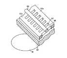
次に、第2の処理ガスノズル32の上方側に配置されるプラズマ発生部80について、詳細に説明する。 Next, the
図4に、本発明の実施形態に係るシリコン窒化膜の成膜方法に用いられる成膜装置のプラズマ発生部の一例の縦断面図を示す。また、図5に、プラズマ発生部の一例の分解斜視図を示す。さらに、図6に、プラズマ発生部に設けられる筐体の一例の斜視図を示す。 FIG. 4 is a longitudinal sectional view showing an example of a plasma generating unit of a film forming apparatus used in the method for forming a silicon nitride film according to the embodiment of the present invention. FIG. 5 is an exploded perspective view of an example of the plasma generating unit. FIG. 6 is a perspective view of an example of a housing provided in the plasma generating unit.
プラズマ発生部80は、金属線等から形成されるアンテナ83をコイル状に例えば鉛直軸回りに3重に巻回して構成されている。また、プラズマ発生部80は、平面視で回転テーブル2の径方向に伸びる帯状体領域を囲むように、且つ回転テーブル2上のウェハWの直径部分を跨ぐように配置されている。 The
アンテナ83は、整合器84を介して周波数が例えば13.56MHz及び出力電力が例えば5000Wの高周波電源85に接続されている。そして、このアンテナ83は、真空容器1の内部領域から気密に区画されるように設けられている。また、アンテナ83と整合器84及び高周波電源85とを電気的に接続するための接続電極86が設けられる。 The
図4及び図5に示すように、第2の処理ガスノズル32の上方側における天板11には、平面視で概略扇形に開口する開口部11aが形成されている。 As shown in FIGS. 4 and 5, the
開口部11aには、図4に示すように、開口部11aの開口縁部に沿って、この開口部11aに気密に設けられる環状部材82を有する。後述する筐体90は、この環状部材82の内周面側に気密に設けられる。即ち、環状部材82は、外周側が天板11の開口部11aに臨む内周面11bに対向すると共に、内周側が後述する筐体90のフランジ部90aに対向する位置に、気密に設けられる。そして、この環状部材82を介して、開口部11aには、アンテナ83を天板11よりも下方側に位置させるために、例えば石英等の誘導体により構成された筐体90が設けられる。 As shown in FIG. 4, the
図6は、プラズマ発生部80の筐体の一例を示した図である。図6に示すように、筐体90は、上方側の周縁部が周方向に亘ってフランジ状に水平に伸び出してフランジ部90aをなすと共に、平面視において、中央部が下方側の真空容器1の内部領域に向かって窪むように形成されている。 FIG. 6 is a diagram illustrating an example of the housing of the
筐体90は、この筐体90の下方にウェハWが位置した場合に、回転テーブル2の径方向におけるウェハWの直径部分を跨ぐように配置されている。なお、環状部材82と天板11との間には、O−リング等のシール部材11cが設けられる。 The
真空容器1の内部雰囲気は、環状部材82及び筐体90を介して気密に設定されている。具体的には、筐体90を開口部11a内に嵌め込み、次いで筐体90の上面であって、筐体90の接触部に沿うように枠状に形成された押圧部材91によって筐体90を下方側に向かって周方向に亘って押圧する。さらに、この押圧部材91を図示しないボルト等により天板11に固定する。これにより、真空容器1の内部雰囲気は気密に設定される。 The internal atmosphere of the
なお、図2に示されるように、筐体90は、第3の処理領域P3、つまり第3の処理ガスノズル33の上方にも設けられる。第3の処理領域P3では、プラズマ発生部80は設けられないが、第2の処理領域P2で窒化ガスが供給されており、第3の処理領域P3で塩素含有ガスを供給するため、異なる2種類のガスの混合を防ぐため、仕切を設ける意味で筐体90のみ設ける。 As shown in FIG. 2, the
図6に示すように、筐体90の下面には、当該筐体90の下方側の処理領域P2、P3の各々を周方向に沿って囲むように、回転テーブル2に向かって垂直に伸び出す突起部92が形成されている。そして、この突起部92の内周面、筐体90の下面及び回転テーブル2の上面により囲まれた領域には、前述した第2の処理ガスノズル32及び第3の処理用ガスノズル33が収納されている。なお、第2の処理ガスノズル32及び第3の処理ガスノズル33の基端部(真空容器1の内壁側)における突起部92は、第2の処理ガスノズル32及び第3の処理ガスノズル33の外形に沿うように概略円弧状に切り欠かれている。 As shown in FIG. 6, the lower surface of the
図4に示すように、筐体90の下方側には、突起部92が周方向に亘って形成されている。シール部材11cは、この突起部92によって、プラズマに直接曝されず、即ち、プラズマ生成領域から隔離されている。そのため、プラズマ生成領域からプラズマが例えばシール部材11c側に拡散しようとしても、突起部92の下方を経由して行くことになるので、シール部材11cに到達する前にプラズマが失活することとなる。 As shown in FIG. 4, a
筐体90の上方側には、当該筐体90の内部形状に概略沿うように形成された導電性の板状体である金属板例えば銅などからなる、接地されたファラデーシールド95が収納されている。このファラデーシールド95は、筐体90の底面に沿うように水平に形成された水平面95aと、この水平面95aの外終端から周方向に亘って上方側に伸びる垂直面95bと、を備えており、平面視で例えば概略六角形となるように構成されていても良い。 On the upper side of the
図7に本実施形態に係るプラズマ発生部の一例の平面図を示し、図8に本実施形態に係るプラズマ発生部に設けられるファラデーシールドの一部を示す斜視図を示す。 FIG. 7 is a plan view of an example of the plasma generating section according to the present embodiment, and FIG. 8 is a perspective view showing a part of a Faraday shield provided in the plasma generating section according to the present embodiment.
回転テーブル2の回転中心からファラデーシールド95を見た場合の右側及び左側におけるファラデーシールド95の上端縁は、各々、右側及び左側に水平に伸び出して支持部96を為している。そして、ファラデーシールド95と筐体90との間には、支持部96を下方側から支持すると共に筐体90の中心部領域C側及び回転テーブル2の外縁部側のフランジ部90aに各々支持される枠状体99が設けられている。 When the
アンテナ83によって生成した電界がウェハWに到達する場合、ウェハWの内部に形成されているパターン(電気配線等)が電気的にダメージを受けてしまう場合がある。そのため、図8に示すように、水平面95aには、アンテナ83において発生する電界及び磁界(電磁界)のうち電界成分が下方のウェハWに向かうことを阻止すると共に、磁界をウェハWに到達させるために、多数のスリット97が形成されている。 When the electric field generated by the
スリット97は、図7及び図8に示すように、アンテナ83の巻回方向に対して直交する方向に伸びるように、周方向に亘ってアンテナ83の下方位置に形成されている。ここで、スリット97は、アンテナ83に供給される高周波に対応する波長の1/10000以下程度の幅寸法となるように形成されている。また、各々のスリット97の長さ方向における一端側及び他端側には、これらスリット97の開口端を塞ぐように、接地された導電体等から形成される導電路97aが周方向に亘って配置されている。ファラデーシールド95においてこれらスリット97の形成領域から外れた領域、即ち、アンテナ83の巻回された領域の中央側には、当該領域を介してプラズマの発光状態を確認するための開口部98が形成されている。なお、前述した図2においては、簡単のために、スリット97を省略しており、スリット97の形成領域例を、一点鎖線で示している。 As shown in FIGS. 7 and 8, the
図5に示すように、ファラデーシールド95の水平面95a上には、ファラデーシールド95の上方に載置されるプラズマ発生部81a、81bとの間の絶縁性を確保するために、厚み寸法が例えば2mm程度の石英等から形成される絶縁板94が積層されている。即ち、プラズマ発生部81a、81bは、各々、筐体90、ファラデーシールド95及び絶縁板94を介して真空容器1の内部(回転テーブル2上のウェハW)を臨むように配置されている。 As shown in FIG. 5, on the
なお、第3の処理領域P3においては、図5に示す筐体90のみが設けられ、プラズマ発生部80を含めた筐体90より上方の部品は設けなくてよい。 In the third processing area P3, only the
再び、本実施形態に係る基板処理装置の他の構成要素について、説明する。 Again, other components of the substrate processing apparatus according to the present embodiment will be described.
回転テーブル2の外周側において、回転テーブル2よりも僅かに下位置には、図2に示すように、カバー体であるサイドリング100が配置されている。サイドリング100の上面には、互いに周方向に離間するように例えば2箇所に排気口61、62が形成されている。別の言い方をすると、真空容器1の床面には、2つの排気口が形成され、これら排気口に対応する位置におけるサイドリング100には、排気口61、62が形成されている。 On the outer peripheral side of the
本明細書においては、排気口61、62のうち一方及び他方を、各々、第1の排気口61、第2の排気口62と呼ぶ。ここでは、第1の排気口61は、分離ガスノズル42と、この分離ガスノズル42に対して、回転テーブルの回転方向下流側に位置する第1のプラズマ発生部81aとの間に形成されている。また、第2の排気口62は、第2のプラズマ発生部81bと、このプラズマ発生部81bよりも回転テーブル2の回転方向下流側の分離領域Dとの間に形成されている。 In this specification, one and the other of the
第1の排気口61は、第1の処理ガスや分離ガスを排気するためのものであり、第2の排気口62は、プラズマ処理用ガスや分離ガスを排気するためのものである。これら第1の排気口61及び第2の排気口62は、各々、バタフライバルブ等の圧力調整部65が介設された排気管63により、真空排気機構である例えば真空ポンプ64に接続されている。 The
前述したように、中心部領域C側から外縁側に亘って筐体90を配置しているため、プラズマ処理領域P2、P3に対して回転テーブル2の回転方向上流側から通流してくるガスは、この筐体90によって排気口62に向かおうとするガス流が規制されてしまうことがある。そのため、筐体90よりも外周側におけるサイドリング100の上面には、ガスが流れるための溝状のガス流路101(図1及び図2参照)が形成されている。 As described above, since the
天板11の下面における中央部には、図1に示すように、凸状部4における中心部領域C側の部位と連続して周方向に亘って概略リング状に形成されると共に、その下面が凸状部4の下面(天井面44)と同じ高さに形成された突出部5が設けられている。この突出部5よりも回転テーブル2の回転中心側におけるコア部21の上方側には、中心部領域Cにおいて各種ガスが互いに混ざり合うことを抑制するためのラビリンス構造部110が配置されている。 As shown in FIG. 1, a central portion of the lower surface of the
前述したように筐体90は中心部領域C側に寄った位置まで形成されているので、回転テーブル2の中央部を支持するコア部21は、回転テーブル2の上方側の部位が筐体90を避けるように回転中心側に形成されている。そのため、中心部領域C側では、外縁部側よりも、各種ガス同士が混ざりやすい状態となっている。そのため、コア部21の上方側にラビリンス構造を形成することにより、ガスの流路を稼ぎ、ガス同士が混ざり合うことを防止することができる。 As described above, since the
より具体的には、ラビリンス構造部110は、回転テーブル2側から天板11側に向かって垂直に伸びる壁部と、天板11側から回転テーブル2に向かって垂直に伸びる壁部とが、各々周方向に亘って形成されると共に、回転テーブル2の半径方向において交互に配置された構造を有する。ラビリンス構造部110では、例えば第1の処理ガスノズル31から吐出されて中心部領域Cに向かおうとする第1の処理ガスは、ラビリンス構造部110を乗り越えていく必要がある。そのため、中心部領域Cに向かうにつれて流速が遅くなり、拡散しにくくなる。結果として、処理ガスが中心部領域Cに到達する前に、中心部領域Cに供給される分離ガスにより、処理領域P1側に押し戻されることになる。また、中心部領域Cに向かおうとする他のガスについても、同様にラビリンス構造部110によって中心部領域Cに到達しにくくなる。そのため、処理ガス同士が中心部領域Cにおいて互いに混ざり合うことが防止される。 More specifically, the
一方、分離ガス供給管51からこの中心部領域Cに供給された分離ガスは、周方向に勢いよく拡散しようとするが、ラビリンス構造部110を設けているため、ラビリンス構造部110を乗り越えるうちに流速が抑えられていく。この場合、窒素ガスは、例えば回転テーブル2と突起部92との間の極めて狭い領域へも侵入しようとするが、ラビリンス構造部110により流速が抑えられているので、例えば搬送アーム10の進退領域等の比較的広い領域へと流れていく。そのため、筐体90の下方側への窒素ガスの流入が抑えられる。 On the other hand, the separation gas supplied to the central region C from the separation
回転テーブル2と真空容器1の底面部14との間の空間には、図1に示すように、加熱機構であるヒータユニット7が設けられている。ヒータユニット7は、回転テーブル2を介して回転テーブル2上のウェハWを例えば室温〜760℃程度に加熱することができる構成となっている。なお、図1において、ヒータユニット7の側方側にカバー部材71a設けられており、ヒータユニット7の上方には、ヒータユニット7の上方側を覆う覆い部材7aが設けられている。また、真空容器1の底面部14には、ヒータユニット7の下方側において、ヒータユニット7の配置空間をパージするためのパージガス供給管73が、周方向に亘って複数個所に設けられている。 As shown in FIG. 1, a heater unit 7 as a heating mechanism is provided in a space between the
真空容器1の側壁には、図2に示すように、搬送アーム10と回転テーブル2との間においてウェハWの受け渡しを行うための搬送口15が形成されている。この搬送口15は、ゲートバルブGより気密に開閉自在に構成されている。 As shown in FIG. 2, a
回転テーブル2の凹部24は、この搬送口15に臨む位置にて搬送アーム10との間でウェハWの受け渡しが行われる。そのため、回転テーブル2の下方側の受け渡し位置に対応する箇所には、凹部24を貫通してウェハWを裏面から持ち上げるための図示しない昇降ピン及び昇降機構が設けられている。 The wafer W is transferred to and from the
また、本実施形態に係る基板処理装置には、装置全体の動作を制御するためのコンピュータからなる制御部120が設けられている。この制御部120のメモリ内には、後述の基板処理を行うためのプログラムが格納されている。このプログラムは、装置の各種動作を実行するようにステップ群が組まれており、ハードディスク、コンパクトディスク、光磁気ディスク、メモリカード、フレキシブルディスク等の記憶媒体である記憶部121から制御部120内にインストールされる。 Further, the substrate processing apparatus according to the present embodiment is provided with a
<シリコン窒化膜の成膜方法>
次に、本発明の実施形態に係るシリコン窒化膜の成膜方法について説明する。まず、上述の成膜装置を用いないプロセスにも適用可能な、本実施形態に係るシリコン窒化膜の成膜方法の原理について説明する。但し、説明は、上述の成膜装置との関係を述べながら説明する。<Method of forming silicon nitride film>
Next, a method for forming a silicon nitride film according to an embodiment of the present invention will be described. First, the principle of the method for forming a silicon nitride film according to the present embodiment, which can be applied to a process that does not use the above-described film forming apparatus, will be described. However, the description will be made while describing the relationship with the above-described film forming apparatus.
図9は、本発明の実施形態に係るシリコン窒化膜の成膜方法の一例を示した図である。図9(a)は、窒化工程の一例を示した図である。窒化工程では、ウェハWに窒化ガスが供給され、基板表面、又は基板表面に既にSiN膜が成膜されている場合にはSiN膜表面の窒化が行われる。窒化ガスは、図9(a)においては、NH3とArの混合ガス、即ちアンモニア含有ガスが用いられている。なお、窒化工程は、成膜対象の表面を窒化し、NH2基を表面に形成できれば、窒化方法は問わないが、プラズマにより窒化ガスを活性化して供給してもよい。上述の成膜装置では、第2の処理領域P2にて、第2の処理ガスノズル32からNH3/Arが供給され、プラズマ発生部80により活性化されてウェハWの表面に供給される。かかる窒化工程により、表面にシリコン含有ガスの吸着サイトが形成される。FIG. 9 is a view showing an example of a method for forming a silicon nitride film according to the embodiment of the present invention. FIG. 9A is a diagram showing an example of the nitriding step. In the nitriding step, a nitriding gas is supplied to the wafer W, and the surface of the substrate or, if an SiN film is already formed on the substrate surface, nitriding of the surface of the SiN film is performed. In FIG. 9A, a mixed gas of NH3 and Ar, that is, an ammonia-containing gas is used as the nitriding gas. Note that in the nitriding step, the nitriding method is not limited as long as the surface of a film formation target is nitrided and an NH2 group can be formed on the surface. In the above-described film forming apparatus, NH3 / Ar is supplied from the second
図9(b)は、非吸着サイト形成工程の一例を示した図である。非吸着サイト形成工程では、ウェハWの表面に塩素含有ガスを供給し、塩素ガスのNH2基への物理吸着により、部分的にシリコン含有ガスの非吸着サイトを形成する。ここで、塩素ガスのNH2基への物理吸着は、NH2基の先端にある水素Hと塩素Clとの電気陰性度の差によるイオン的な吸着である。FIG. 9B is a diagram illustrating an example of the non-adsorption site forming step. In the non-adsorption site forming step, a chlorine-containing gas is supplied to the surface of the wafer W, and the non-adsorption site of the silicon-containing gas is partially formed by physical adsorption of the chlorine gas to the NH2 group. Here, the physical adsorption of chlorine gas to the NH2 group is ionic adsorption due to the difference in electronegativity between hydrogen H and chlorine Cl at the tip of the NH2 group.
図10は、塩素と水素の電気陰性度の差を説明するための図である。図10(a)は、代表的な元素の電気陰性度を示した図である。図10(a)において、横軸は族、縦軸は周期、鉛直軸は電気陰性度の大きさを示している。図10(a)に示されるように、各元素は、種々の電気陰性度を有する。 FIG. 10 is a diagram for explaining a difference in electronegativity between chlorine and hydrogen. FIG. 10A is a diagram showing the electronegativity of a representative element. In FIG. 10A, the abscissa represents the group, the ordinate represents the period, and the vertical axis represents the magnitude of electronegativity. As shown in FIG. 10A, each element has various electronegativities.
図10(b)は、塩素及び水素の電気陰性度を含む所定の元素の電気陰性度を示した一覧表である。図10(b)に示されるように、塩素の電気陰性度は3.0であり、水素の電気陰性度は2.1であるので、両者の電気陰性度の差は0.9である。 FIG. 10B is a table showing the electronegativities of predetermined elements including the electronegativities of chlorine and hydrogen. As shown in FIG. 10B, since the electronegativity of chlorine is 3.0 and the electronegativity of hydrogen is 2.1, the difference between the two is 0.9.
図10(c)は、所定の原子間の結合エネルギーと電気陰性度の差を示した一覧表である。図10(b)で説明した通り、H−Cl間の電気陰性度の差は0.9であり、Si−F間の2.2、Si−O間の1.7よりは小さいが、Si−H間の0.3よりは大きい値である。よって、あまり強くは無いが、ある程度の吸引力で吸着している、というレベルにあると考えられる。 FIG. 10C is a list showing the difference between the bond energy between predetermined atoms and the electronegativity. As described with reference to FIG. 10B, the difference in electronegativity between H—Cl is 0.9, which is smaller than 2.2 between Si—F and 1.7 between Si—O. This is a value larger than 0.3 between -H. Therefore, although it is not very strong, it is considered to be at the level of being adsorbed by a certain suction force.
図9(b)に戻る。図9(b)に示されるように、非吸着サイト形成工程では、水素に塩素が物理吸着する状態となる。なお、塩素の吸着は総てのNH2基に行う訳ではなく、所定の領域にのみ選択的に行われる。NH2基が平坦面上に形成されていると、そのような選択的な非吸着サイトの形成は困難であるが、ウェハWの表面に形成されたトレント、ビアホール等の窪みに埋め込み成膜を行う場合には、塩素は必ずしも窪みの奥まで到達せず、窪みの上部にのみ非吸着サイトを形成することが可能となる。なお、この点の詳細については後述する。Returning to FIG. As shown in FIG. 9B, in the non-adsorption site forming step, chlorine is physically adsorbed on hydrogen. The adsorption of chlorine is not performed on all NH2 groups, but is selectively performed only on a predetermined region. If the NH2 group is formed on a flat surface, it is difficult to form such a selective non-adsorption site. However, it is difficult to form a film by burying in a dent such as a torrent or a via hole formed on the surface of the wafer W. In this case, the chlorine does not necessarily reach the depth of the depression, and a non-adsorption site can be formed only in the upper portion of the depression. The details of this point will be described later.
また、非吸着サイド形成工程は、上述の成膜装置を用いる場合には、第3の処理領域P3において、第3の処理ガスノズル33から塩素含有ガスが供給されることにより行われる。図9(b)においては、Cl2/Arの混合ガスが供給された例が示されている。また、非吸着サイト形成工程では、物理吸着により塩素ガスをNH2基に吸着させるため、プラズマは用いないのが一般的である。上述の成膜装置においても、第3の処理領域P3ではプラズマ発生部80を設けていない。Further, the non-adsorption side forming step is performed by supplying a chlorine-containing gas from the third
図9(c)は、成膜工程の一例を示した図である。成膜工程では、ウェハWにシリコン含有ガスが供給される。シリコン含有ガスは、吸着サイトであるNH2基に吸着し、非吸着サイトであるCl2が吸着した領域には吸着しない。よって、選択的にシリコン含有ガスの吸着が行われる。吸着したシリコン含有ガスは、HClが抜け、化学反応により表面上に堆積し、SiN膜が成膜される。なお、シリコン含有ガスは、図9(c)においては、DCSが用いられた例が挙げられている。FIG. 9C is a diagram illustrating an example of a film forming process. In the film forming process, a silicon-containing gas is supplied to the wafer W. The silicon-containing gas is adsorbed on the NH2 group, which is an adsorption site, and is not adsorbed on a region where Cl2, which is a non-adsorption site, is adsorbed. Thus, the silicon-containing gas is selectively adsorbed. HCl adsorbs the adsorbed silicon-containing gas, deposits on the surface by a chemical reaction, and a SiN film is formed. FIG. 9C shows an example in which DCS is used as the silicon-containing gas.
成膜工程は、上述の成膜装置では、第1の処理領域P1にて、第1の処理ガスノズル31からシリコン含有ガスが供給されることにより行われる。また、NH2基に物理吸着した塩素は、あまり強い吸着ではないので、徐々に吸着が解けて減少してゆき、消滅してしまう。例えば、上述の成膜装置では、ウェハWが分離領域Dを通過し、分離ガスが供給されてパージされた段階で吹き飛ばされて消滅する場合が多い。The film forming step is performed by supplying a silicon-containing gas from the first
図9(a)〜(c)に示した窒化工程、非吸着サイド形成工程、成膜工程を順次繰り返すことにより、徐々にSiN膜が堆積し、成膜が進行することになる。 By sequentially repeating the nitriding step, the non-adsorption side forming step, and the film forming step shown in FIGS. 9A to 9C, the SiN film is gradually deposited, and the film formation proceeds.
このようなウェハWへのガスの供給が可能であれば、処理室内に、時間の経過とともに切り替えて供給することにより、本実施形態に係る成膜方法を実施することができる。よって、本実施形態に係る成膜方法は、上述の成膜装置に限らず、種々の成膜装置で実施可能である。 If such a gas supply to the wafer W is possible, the film formation method according to the present embodiment can be performed by switching and supplying the gas into the processing chamber over time. Therefore, the film forming method according to the present embodiment is not limited to the above-described film forming apparatus, and can be performed by various film forming apparatuses.
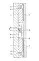
図11は、図9及び図10で説明した成膜方法の原理を用いて、ウェハWの表面に形成された窪みに埋め込みを行う成膜方法の一例を示した図である。 FIG. 11 is a diagram showing an example of a film forming method for embedding in a depression formed on the surface of the wafer W using the principle of the film forming method described with reference to FIGS.
図11(a)は、ウェハWに形成された窪み130の一例を示した図である。図11(a)に示されるように、ウェハWの表面には、トレンチ、ビアホール等の窪み130が形成されている。窪み130は、一般的には、何らかのパターンを形成するように構成されている。ウェハWの窪み130内も含めた表面には、例えば、OH基が形成されている。 FIG. 11A is a diagram illustrating an example of the
図11(b)は、窒化工程の一例を示した図である。窒化工程においては、ウェハWの表面に窒化ガスが供給され、窪み130内全体を含むウェハWの表面が窒化される。窒化工程により、ウェハWの窪み130内を含む表面全体にNH2基が形成される。FIG. 11B is a diagram illustrating an example of the nitriding step. In the nitriding step, a nitriding gas is supplied to the surface of the wafer W, and the surface of the wafer W including the entire inside of the
図11(c)は、非吸着サイト形成工程の一例を示した図である。非吸着サイト形成工程では、ウェハWの表面に塩素含有ガスが供給され、塩素ガスが窪み130の表面から所定深さの上部の範囲に吸着する。上述のように、NH2基のHにClが物理吸着し、一時的に非吸着サイトが形成される。なお、塩素の深さ方向の吸着は、上述の成膜装置であれば、回転テーブル2の回転速度、塩素含有ガスの流量等により調整可能である。つまり、長時間に亘り塩素含有ガスが供給されれば、塩素ガスは窪み130の底面まで吸着してしまい、窪み130の上部にのみ非吸着サイトを形成することができなくなるが、塩素含有ガスが供給されている時間を適度に短くすることにより、窪み130の上部にのみ塩素ガスが物理吸着する状態を作り出すことができる。なお、これは、ガスの切り替えにより本実施形態に係る成膜方法を行う場合も同様であり、ガスの切り替え時間を調整することにより、窪み130の上部にのみ塩素が物理吸着する状態を作り出すことができる。FIG. 11C is a diagram illustrating an example of the non-adsorption site forming step. In the non-adsorption site forming step, a chlorine-containing gas is supplied to the surface of the wafer W, and the chlorine gas is adsorbed in a range above the surface of the
非吸着サイト形成工程により、窪み130の上端から所定深さまでの範囲の上端部にのみ非吸着サイトを形成し、それよりも下方にはNH2基の吸着サイトを残すことができる。By the non-adsorption site forming step, non-adsorption sites can be formed only at the upper end portion in the range from the upper end of the
図11(d)は、成膜工程の一例を示した図である。成膜工程においては、ウェハWの表面にシリコン含有ガスが供給され、吸着サイトにシリコン含有ガスが吸着し、化学反応によりシリコン窒化膜が生成され、堆積する。上述のように、窪み130内の上部の所定領域には非吸着サイトが形成されているが、それ以外の領域は吸着サイトであるNH2基が形成されているので、シリコン窒化膜は、窪み130内の上部には成膜されず、底面を含む下部にのみ成膜される。よって、図11(d)の下段に示すように、窪み130内の底面部を含む下部が厚く、上部が薄いボトムアップ成膜を行うことができる。FIG. 11D is a diagram illustrating an example of the film forming process. In the film forming process, a silicon-containing gas is supplied to the surface of the wafer W, the silicon-containing gas is adsorbed on the adsorption site, and a silicon nitride film is generated and deposited by a chemical reaction. As described above, a non-adsorption site is formed in a predetermined region in the upper portion of the
なお、図11(d)においては、シリコン含有ガスとして、DCSを用いた例を示している。 FIG. 11D shows an example in which DCS is used as the silicon-containing gas.
図11(b)〜(d)に示した窒化工程、非吸着サイト形成工程及び成膜工程を繰り返すことにより、図11(d)の下段に示すように、V字の断面形状を有する開口形状を維持しつつ、埋め込み特性の良好な成膜を行うことができる。これにより、ボイドやシームの発生を抑制しつつ窪み130を埋め込むことができ、ステップカバレージ(段差被覆性、埋め込み特性)の良好な埋め込み成膜を行うことができる。 By repeating the nitriding step, the non-adsorption site forming step, and the film forming step shown in FIGS. 11B to 11D, the opening shape having a V-shaped cross-sectional shape as shown in the lower part of FIG. , And film formation with good embedding characteristics can be performed. Accordingly, the
次に、本発明の実施形態に係る成膜方法を創作するまでに行った実験及び実施例について説明する。 Next, a description will be given of experiments and examples performed up to creation of the film forming method according to the embodiment of the present invention.
図12は、塩素の吸着阻害効果を確認するために行った実験結果を示した図である。塩素の吸着阻害効果を確認するため、塩素を供給しないSiN成膜プロセスと、塩素を供給するSiN成膜プロセスを実施し、両者を比較した。なお、塩素を供給しないSiN成膜プロセスは、非吸着サイト形成工程を設けない成膜プロセスを意味し、塩素を供給するSiN成膜プロセスとは、図9乃至11で説明した本発明の実施形態に係るSiN成膜プロセスである。 FIG. 12 is a diagram showing the results of an experiment performed to confirm the effect of inhibiting adsorption of chlorine. In order to confirm the effect of inhibiting chlorine adsorption, a SiN film forming process not supplying chlorine and a SiN film forming process supplying chlorine were performed, and both were compared. Note that the SiN film forming process that does not supply chlorine means a film forming process that does not include a non-adsorption site forming step, and the SiN film forming process that supplies chlorine is the embodiment of the present invention described with reference to FIGS. The SiN film forming process according to the above.
なお、実験は、上述の回転テーブル式のALD成膜装置を用いて、500℃のウェハ温度、0.75Torrの圧力、回転テーブル2の回転速度5rpmの条件下で行った。また、シリコン含有ガスとしては、DCS1000sccmとキャリアガスのN2ガス500sccmを供給した。窒化ガスは、Ar/NH3の混合ガスをそれぞれ2000/300sccmで供給し、プラズマ発生部80の出力は5kWとした。また、塩素含有ガスは、Ar/Cl2の混合ガスをそれぞれ2000/300sccmの流量で供給した。上述のように、塩素含有ガスの供給では、プラズマは使用しなかった。また、成膜時間は4200秒である。The experiment was performed using the above-described ALD film forming apparatus of a rotary table under the conditions of a wafer temperature of 500 ° C., a pressure of 0.75 Torr, and a rotation speed of the rotary table 2 of 5 rpm. As the silicon-containing gas and theN 2 gasis supplied 500sccm of DCS1000sccm and carrier gas. As the nitriding gas, a mixed gas of Ar / NH3 was supplied at 2000/300 sccm, respectively, and the output of the
図12において、横軸は成膜時間(秒)、縦軸はSiN膜の厚さ(nm)を示し、特性Aが塩素供給なし、特性Bが塩素供給ありの条件である。なお、ウェハWの表面に窪み130は形成されておらず、平坦面上への成膜を行った。図12に示される通り、塩素を供給しない特性Aよりも、塩素を供給した特性Bの膜厚が大幅に小さくなっており、塩素にDCSの吸着を阻害する効果があることが示された。 In FIG. 12, the horizontal axis represents the film formation time (second), the vertical axis represents the thickness (nm) of the SiN film, and the characteristic A is the condition without chlorine supply and the characteristic B is the condition with chlorine supply. The
図13は、塩素の流量と、シリコン含有ガスの吸着阻害効果との関係を説明するための図である。供給する塩素の流量を変化させ、成膜されるSiN膜の膜厚及び面内均一性がどのような影響を受けるかについて実験を行った。なお、実験条件は、塩素ガス以外の条件は、図12で説明した条件と同様である。また、塩素ガスは、ともに供給されるArは2000sccmで一定とし、0、6、10、50、300sccmと変化させて実験を行った。 FIG. 13 is a diagram for explaining the relationship between the flow rate of chlorine and the effect of inhibiting adsorption of a silicon-containing gas. Experiments were conducted on how the flow rate of supplied chlorine was changed and how the film thickness and in-plane uniformity of the formed SiN film were affected. The experimental conditions other than the chlorine gas are the same as those described with reference to FIG. The experiment was carried out with the chlorine gas supplied at a constant Ar of 2000 sccm and varying 0, 6, 10, 50 and 300 sccm.
図13(a)は、塩素の流量とSiN膜の膜厚の関係を示した図である。図13(a)に示されると取り、塩素の流量を増加させるにつれてSiN膜の膜厚が小さくなっており、塩素の流量が多い程、デポジション・レートは低下することが示された。 FIG. 13A is a diagram showing the relationship between the flow rate of chlorine and the thickness of the SiN film. FIG. 13A shows that as the flow rate of chlorine increases, the thickness of the SiN film decreases, and the deposition rate decreases as the flow rate of chlorine increases.
図13(b)は、塩素の流量とSiN膜のY軸上(回転テーブルの半径方向に平行で、ウェハWの中心を通る軸)の膜厚を示した図である。また、塩素の流量が0、6、10、50、300sccmの場合を、特性A、B、C、D、Eで各々示している。図13(b)に示される通り、回転テーブル2の外周側では、塩素を供給したB〜Eでは総てDCSの吸着を阻害する効果が見られるが、それは膜厚3mm程度までであり、それより厚い膜厚では、効果が発揮されず、回転テーブル2の中心側の位置では、塩素の流量が少なくなるにつれて膜厚が大きくなっている。しかしながら、塩素の流量が300sccmの場合には、Y軸上の総てにおいて3mm前後の膜厚が保たれており、十分な吸着阻害効果と面内均一性が得られている。 FIG. 13B is a diagram showing the flow rate of chlorine and the thickness of the SiN film on the Y-axis (an axis parallel to the radial direction of the rotary table and passing through the center of the wafer W). The characteristics A, B, C, D, and E indicate the cases where the flow rates of chlorine are 0, 6, 10, 50, and 300 sccm, respectively. As shown in FIG. 13 (b), on the outer peripheral side of the
このように、図13の実験結果によれば、供給する塩素の流量が大きい程、デポジション・レートは低下することが示された。 Thus, the experimental results of FIG. 13 indicate that the deposition rate decreases as the flow rate of supplied chlorine increases.
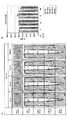
図14は、図13と同様の塩素の流量を変化させる実験を、表面にトレンチ状の窪み130が形成されたウェハWに対して行った結果を示した図である。なお、形成されたトレンチは、開口幅が250nm、深さが2100nmであり、アスペクト比が8.4であった。また、塩素の流量が50sccmの場合については、実験を行わず、塩素の流量が0、6、10、300sccmの場合の結果について示してある。 FIG. 14 is a view showing a result of performing an experiment in which the flow rate of chlorine is changed as in FIG. 13 on a wafer W having a trench-shaped
図14(a)は、実験結果のSEM画像を示している。図14(a)において、トレンチの断面を深さ方向に沿って上端からTOP/T−Side、CTR−T、CTR−B、BTMの4つの領域に区分して示している。なお、CTR−Tは深さ0.6μmの位置、CTR−Bは深さ1.2μmの位置、BTMは深さ2.0μmの位置を示している。 FIG. 14A shows an SEM image of the experimental result. In FIG. 14A, the cross section of the trench is divided into four regions TOP / T-Side, CTR-T, CTR-B, and BTM from the upper end along the depth direction. CTR-T indicates a position at a depth of 0.6 μm, CTR-B indicates a position at a depth of 1.2 μm, and BTM indicates a position at a depth of 2.0 μm.
塩素流量が0、6、10、300sccmの各例において、窪み130の上端付近のウェハWの平坦面の表面(TOP)の膜厚を100%とし、これに対して、T−Side、CTR−T、CTR−B、BTMが何%の膜厚を有するかを示している。 In each example in which the chlorine flow rate is 0, 6, 10, and 300 sccm, the film thickness of the flat surface (TOP) of the wafer W near the upper end of the
図14(a)において、塩素を供給しない場合には、トレンチ内の膜厚はいずれも100%未満であり、しかもトレンチの底面に近付く程膜厚は小さくなっている。よって、上端の開口部を塞ぎやすい成膜結果となっている。 In FIG. 14A, when chlorine is not supplied, the film thickness in each of the trenches is less than 100%, and the film thickness becomes smaller as approaching the bottom surface of the trench. Therefore, a film formation result that the opening at the upper end is easily closed is obtained.
一方、塩素を6sccmの流量で供給した場合は、BTMは99%で100%よりやや薄くなっているものの、CTR−Bで103%と上端付近表面よりも厚く成膜され、CTR−T、T−Sideでは96%、97%とこれよりも薄く成膜されている。よって、V字断面形状の開口を有する埋め込み特性の良好な成膜状態となっている。 On the other hand, when chlorine is supplied at a flow rate of 6 sccm, BTM is 99% and slightly thinner than 100%, but CTR-B is 103% thicker than the surface near the upper end, and CTR-T, TTR In the case of -Side, the film is formed as thin as 96% or 97%. Accordingly, a film is formed in a film having an opening having a V-shaped cross section and excellent burying characteristics.
同様に、塩素を10sccmの流量で供給した場合は、BTMは99%で100%よりやや薄くなっているものの、CTR−Bで108%、CTR−Tで109%と上端付近表面よりもかなり厚く成膜され、T−Sideでは100%とこれよりも薄く成膜されている。よって、6sccmの実施例程ではないものの、V字断面形状の開口を有する埋め込み特性の良好な成膜状態となっていると言える。 Similarly, when chlorine is supplied at a flow rate of 10 sccm, BTM is 99% and slightly thinner than 100%, but is 108% in CTR-B and 109% in CTR-T, which is considerably thicker than the surface near the upper end. The film is formed, and in T-Side, the film is formed as thin as 100%. Therefore, although not as large as in the example of 6 sccm, it can be said that the film is in a film-forming state having an opening having a V-shaped cross section and excellent burying characteristics.
塩素を300sccmの流量で供給した場合には、BTMが88%、CTR−B及びCTR−Tが90%、T−Sideが78%と、全体的に膜厚が薄いが、BTM、CTR−B及びCTR−TよりもT−Sideが薄く成膜され、V字断面形状に近い状態となっていると言える。 When chlorine is supplied at a flow rate of 300 sccm, BTM is 88%, CTR-B and CTR-T are 90%, and T-Side is 78%. It can be said that T-Side is formed thinner than CTR-T and CTR-T, and is in a state close to a V-shaped cross section.
図14(b)は、図14(a)の結果をグラフで示した図である。図14(b)に示される通り、塩素の流量が6sccm、10sccmの場合には、TOP、T−SideよりもCTR−Bの膜厚が大きくなり、埋め込み特性の良好な成膜がなされている。一方、塩素を供給しない場合には、底面から上端に向かって膜厚が少しずつ厚くなっており、コンフォーマルではあるが、埋め込み特性はあまり良くなく、V字断面形状は形成されていない。 FIG. 14B is a graph showing the result of FIG. 14A. As shown in FIG. 14B, when the flow rate of chlorine is 6 sccm and 10 sccm, the film thickness of CTR-B is larger than that of TOP or T-Side, and a film having good filling characteristics is formed. . On the other hand, when chlorine is not supplied, the film thickness is gradually increased from the bottom to the upper end, and although the film is conformal, the embedding characteristics are not so good, and the V-shaped cross-sectional shape is not formed.
塩素の流量が300sccmの場合には、T−SideよりもCTR−T、CTR−B、BTMの膜厚が大きく、ややV字断面形状となっているが、底面側の膜厚が低下し、埋め込み特性が良好ではない状態である。 When the flow rate of chlorine is 300 sccm, the film thickness of CTR-T, CTR-B, and BTM is larger than that of T-Side and has a slightly V-shaped cross section, but the film thickness on the bottom surface side is reduced, The embedding characteristics are not good.
このように、図14の実施例によれば、成膜中に塩素を供給し、かつ塩素の流量を調整することにより、成膜時のV字断面形状及び埋め込み特性を適切に向上させることができることが示された。 As described above, according to the embodiment of FIG. 14, by supplying chlorine during film formation and adjusting the flow rate of chlorine, it is possible to appropriately improve the V-shaped cross-sectional shape and the filling characteristics during film formation. It was shown that it could be done.
図15は、塩素の吸着が物理吸着であることを確認するために行った実験の結果を示した図である。図15に係る実験では、本実施形態に係る1サイクル中で塩素を供給する工程を有するプロセスと、SiN膜をまず成膜してしまい、その後に塩素を供給し、そしてまたSiN膜を成膜し、その後に塩素を供給するという、SiN成膜と塩素供給を2ステップで行う2ステッププロセスとを行った。 FIG. 15 is a diagram showing the results of an experiment performed to confirm that the adsorption of chlorine is physical adsorption. In the experiment according to FIG. 15, a process including a step of supplying chlorine in one cycle according to the present embodiment, an SiN film is formed first, then chlorine is supplied, and then a SiN film is formed. Then, a two-step process of supplying Si and performing chlorine film formation and chlorine supply in two steps was performed.
図15において、左側のNormalが本実施形態に係る成膜方法、右側の2Stepが2ステップの成膜方法の実施結果である。なお、成膜条件は、ウェハ温度が500℃、処理室内の圧力が0.75Torr、回転速度は5rpmである。本実施形態に係る成膜方法では、今までの成膜条件と同様であるが、2ステップの成膜方法では、成膜ステップでは、シリコン含有ガスとして、DCS/N2(キャリアガス)を各々1000/500sccmで供給し、窒化ガスとしてAr/NH3を2000/300sccmで供給し、1サイクル120秒を35サイクル繰り返した。なお、プラズマの出力は5kWであった。In FIG. 15, “Normal” on the left is the result of the film forming method according to the present embodiment, and “2Step” on the right is the result of the film forming method in two steps. The film formation conditions are as follows: the wafer temperature is 500 ° C., the pressure in the processing chamber is 0.75 Torr, and the rotation speed is 5 rpm. The film forming method according to the present embodiment is the same as the film forming conditions up to now, but in the two-step film forming method, DCS / N2 (carrier gas) is used as the silicon-containing gas in the film forming step. The gas was supplied at 1000/500 sccm, and Ar / NH3 was supplied at 2000/300 sccm as a nitriding gas, and one cycle for 120 seconds was repeated 35 times. The output of the plasma was 5 kW.
また、塩素供給ステップは、Ar/Cl2の混合ガスを2000/6sccm、プラズマを発生させずに供給した。2秒のサイクルと、4秒のサイクルの2パターンを、各々35サイクル繰り返した。120秒成膜、2秒塩素供給を1サイクルとし、35サイクル繰り返す2ステッププロセスと、120秒成膜、4秒塩素供給を1サイクルとし、35サイクル繰り返す2ステッププロセスの双方を実施した。In the chlorine supply step, a mixed gas of Ar / Cl2 was supplied at 2000/6 sccm without generating plasma. Two patterns of a cycle of 2 seconds and a cycle of 4 seconds were repeated 35 cycles each. Both a two-step process in which 120 seconds of film formation and two seconds of chlorine supply were defined as one cycle and 35 cycles were repeated, and a two-step process in which 120 seconds of film formation and four seconds of chlorine supply were defined as one cycle and were repeated 35 cycles were performed.
図15に示されるように、実施形態の塩素を6sccm供給する成膜方法のみ膜厚が低下しているが、本実施例から塩素供給ステップ(非吸着サイト形成工程)を無くしたプロセスと、2ステップのプロセスは、ほぼ同様の膜厚となった。これは、2ステッププロセスを実施しても、塩素を供給しないプロセスと同じ効果しか無かったことを意味する。つまり、2ステッププロセスで塩素をウェハWに供給しても、シリコン含有ガスの吸着阻害効果は得られないことを意味する。これは、塩素を供給しても、塩素供給ステップと成膜ステップとの間のパージガス(分離ガス)の供給で塩素が吹き飛ばされていることを意味する。つまり、塩素の吸着は、化学反応による吸着ではなく、一時的に吸着しているに過ぎない物理的吸着であることを意味する。よって、塩素の供給により、成膜は一時阻害されるが、飽くまで一時的な阻害であり、次にシリコン含有ガスが供給される際にシリコン含有ガスを阻害する機能しか有しない。よって、非吸着サイトの形成領域(窪み130内の深さ)を制御することにより、全体の成膜は阻害することなく、一時的な阻害により、V字断面形状を形成しながら埋め込み成膜を行うことが可能となる。 As shown in FIG. 15, the film thickness is reduced only in the film forming method of supplying chlorine of 6 sccm according to the embodiment. The step process resulted in substantially the same film thickness. This means that the two-step process had the same effect as the process without chlorine supply. That is, even if chlorine is supplied to the wafer W in the two-step process, the effect of inhibiting adsorption of the silicon-containing gas cannot be obtained. This means that even when chlorine is supplied, chlorine is blown off by the supply of the purge gas (separation gas) between the chlorine supply step and the film formation step. That is, the adsorption of chlorine means not the adsorption by a chemical reaction but the physical adsorption that is only temporarily adsorbed. Thus, the supply of chlorine temporarily hinders the film formation, but is only a temporary hindrance until it is saturated, and has only the function of inhibiting the silicon-containing gas when the silicon-containing gas is subsequently supplied. Therefore, by controlling the formation region (depth in the recess 130) of the non-adsorption site, the entire film formation is not hindered, and the temporary film hinders the embedded film formation while forming the V-shaped cross-sectional shape. It is possible to do.
本発明の実施形態に係る成膜方法は、このような塩素ガスの物理的吸着を巧みに利用して開口を塞がない埋め込み特性の良好な成膜を実現していると言える。 It can be said that the film forming method according to the embodiment of the present invention realizes film forming with good filling characteristics that does not close the opening by skillfully utilizing such physical adsorption of chlorine gas.
図16は、本発明の実施形態に係るSiN膜の成膜方法を、回転テーブル2の回転速度を変化させて実施した結果を示した図である。成膜条件は、今までと同様であり、ウェハ温度500℃、真空容器1内の圧力が0.75Torrである。また、シリコン含有ガスは、DCS/N2(キャリアガス)を1000/500sccmで供給し、窒化ガスAr/NH3を2000/6sccmで供給した。プラズマ発生部80の出力は5kWであった。また、塩素含有ガスは、Ar/Cl2を2000/6sccmの流量で供給した。回転テーブル2の回転速度を5、15、30、60rpmに変化させ、4200秒間成膜を行った。FIG. 16 is a diagram showing a result of executing the method of forming the SiN film according to the embodiment of the present invention while changing the rotation speed of the
図16に示されるように、回転テーブル2の回転速度が高い程、デポジション・レートは増加することが分かる。 As shown in FIG. 16, the higher the rotation speed of the
図17は、図16で説明した実施結果の窪みの埋め込み特性を示した図である。図17(a)は、図16で説明した条件で、回転テーブル2の回転速度を変化させてウェハWに形成されたトレンチへの埋め込み成膜を実施した結果のSEM画像を示した図である。なお、各実施例において、TOPの膜厚を100%とし、それを基準としてT−Side、CRT−T、CRT−B、BTMの膜厚を示している点は、図14(a)における説明と同様である。 FIG. 17 is a diagram showing the embedding characteristics of the depression as a result of the embodiment described with reference to FIG. FIG. 17A is a diagram showing an SEM image of a result of performing burying film formation in a trench formed in the wafer W by changing the rotation speed of the
図17(a)において、回転速度が5rpmの場合、BTMが99%とTOPとほぼ同様の膜厚となり、CTR−Bが103%とTOPよりも厚い膜厚となっている。更に、CTR−T、T−Sideはそれぞれ96%、97%であり、下部よりも薄い膜厚となっている。よって、回転速度が5rpmの実施例では、V字断面形状を有する埋め込み特性の良好な成膜を行うことができた。 In FIG. 17A, when the rotation speed is 5 rpm, the BTM is 99%, which is almost the same as TOP, and the CTR-B is 103%, which is larger than TOP. Furthermore, CTR-T and T-Side are 96% and 97%, respectively, which are thinner than the lower part. Therefore, in the example in which the rotation speed was 5 rpm, a film having a V-shaped cross-sectional shape and excellent embedding characteristics could be formed.
一方、回転テーブル2の回転速度が15、30、60rpmの実施例では、BTM、CTR−B、CTR−Tの膜厚が、いずれもT−Sideの膜厚よりも薄く、V字形状断面を形成しつつ埋め込み成膜を行うことはできなかった。 On the other hand, in the embodiment in which the rotation speed of the
図17(b)は、図17(a)の結果をグラフ化して示した図である。図17(b)に示される通り、回転テーブル2の回転速度が5rpmの実施例では、膜厚が厚く、かつ底部側の方が上部側よりも膜厚が厚く、良好な埋め込み特性が得られている。一方、回転テーブル2の回転速度が15、30、60rpmの場合には、底面側の埋め込み特性が必ずしも良好ではなく、5rpmの結果と比較して、必ずしも良好な埋め込み特性は得られなかった。 FIG. 17B is a graph showing the result of FIG. 17A. As shown in FIG. 17 (b), in the embodiment in which the rotation speed of the
このように、良好な埋め込み特性を実現するためには、回転テーブル2の回転速度を適切に調整する方が好ましく、回転速度は、15rpmよりも低い値が好ましく、例えば5rpm、6rpmといった回転速度が適切であることが示された。 As described above, in order to realize good embedding characteristics, it is preferable to appropriately adjust the rotation speed of the
次に、図9及び図11を主に用いて、上述の回転テーブル式の成膜装置を用いた本発明の実施形態に係るSiN膜の成膜方法について、ウェハWの搬送等の動作も含めて説明する。 Next, mainly with reference to FIGS. 9 and 11, a method of forming a SiN film according to an embodiment of the present invention using the above-described rotary table type film forming apparatus, including an operation such as transfer of a wafer W, will be described. Will be explained.
先ず、上述した基板処理装置へのウェハWの搬入に際しては、先ず、ゲートバルブGを開放する。そして、回転テーブル2を間欠的に回転させながら、図示しない搬送アームにより搬送口15を介して回転テーブル2上に載置する(図2参照)。なお、ウェハWの表面には、トレンチ、ビアホール等の窪み130が形成されている。 First, when carrying the wafer W into the above-described substrate processing apparatus, first, the gate valve G is opened. Then, while rotating the
次いで、ゲートバルブGを閉じて、ヒータユニット7により、ウェハWを所定の温度に加熱する。続いて、第1の処理ガスノズル31からシリコン含有ガスを所定の流量で吐出すると共に、第2の処理ガスノズル32からは窒化ガスを所定の流量で吐出する。また、第3の処理ガスノズル33からは、所定の流量で塩素含有ガスを供給する。 Next, the gate valve G is closed, and the wafer W is heated to a predetermined temperature by the heater unit 7. Subsequently, a silicon-containing gas is discharged from the first
そして、圧力調整部65により真空容器1内を所定の圧力に調整する。また、プラズマ発生部80では、アンテナ83に対して、所定の出力の高周波電力を印加する。 Then, the inside of the
ウェハWの表面では、回転テーブル2の回転によって第2の処理領域P2において、プラズマ発生部80により活性化された窒化ガスが第2の処理ガスノズル32からウェハWの表面に供給され、窪み130も含めてウェハWの表面全体が窒化される。これにより、ウェハWの表面にNH2基の吸着サイトが形成される。On the surface of the wafer W, the nitriding gas activated by the
ウェハWは次に、回転テーブル2の回転により、第3の処理領域P3を通過する。第3の処理領域P3では、第3の処理ガスノズル33から供給された塩素含有ガスがウェハWの表面に供給され、窪み130の上部の所定領域に塩素が物理吸着し、非吸着サイトが窪み130の上部の所定領域に形成される。なお、上部の所定領域は、ウェハWの平坦面から所定深さを有する窪み130内の上部領域である。上部の所定領域の所定深さは、塩素の供給流量及び回転テーブル2の回転速度により調整される。なお、塩素の流量は例えば0sccmより大きく10sccm以下の範囲が好ましく、0sccmより大きく6sccm以下の範囲と、5sccm以上10sccm以下の範囲がより好ましい。また、塩素の流量は、5sccm以上6sccm以下の範囲にあることが更に好ましい。 Next, the wafer W passes through the third processing area P3 due to the rotation of the
また、回転テーブル2の回転速度は、0rpmより高く15rpm未満であることが好ましく、0rpmより高く6pm以下の範囲又は5rpm以上15rpm未満の範囲であることがより好ましい。また、回転テーブル2の回転速度は、5rpm以上6rpmであることが更に好ましい。 The rotation speed of the
ウェハWは次に、回転テーブル2の回転により、分離領域Dを通過する。分離領域Dでは、分離ガスノズル41から供給された分離ガスにより、ウェハWの表面がパージされ、清浄化される。なお、分離ガスは、例えば、窒素ガス又はアルゴンガスであってもよい。 Next, the wafer W passes through the separation region D by the rotation of the
ウェハWは次に、回転テーブル2の回転により、第1の処理領域P1を通過する。第1の処理領域P1では、第1の処理ガスノズル31から供給されたシリコン含有ガスがウェハWの表面に供給され、窪み130内の底面付近を含む吸着サイト(NH2基)に吸着し、化学反応により反応生成物であるSiNの分子層が窪み130の下部に堆積する。Next, the wafer W passes through the first processing area P1 due to the rotation of the
次にウェハWは、回転テーブル2の回転により、分離領域Dを通過する。分離領域Dでは、ウェハWの表面に分離ガスが供給され、ウェハWの表面が清浄化される。 Next, the wafer W passes through the separation region D by the rotation of the
回転テーブル2の回転を続けることにより、ウェハW表面の窒化による吸着サイトの形成(窒化工程)、窪み130内の上部の所定領域での非吸着サイトの形成(非吸着サイト形成工程)、ウェハWの表面のパージ(パージ工程)、シリコン含有ガスの吸着サイトへの吸着及び反応生成物の生成(成膜工程)、ウェハWの表面のパージ(パージ工程)が周期的に複数回行われる。そして、窪み130内にV字断面形状を形成しつつ埋め込み成膜が行われ、SiN膜が窪み130内に埋め込まれてゆく。窪み130の上端の開口を塞がず、V字形状を維持しつつ埋め込み成膜が行われるので、ボイドやシームの発生を抑制しつつ窪み130をSiN膜で埋め込むことができる。 By continuing the rotation of the
このように、本発明の実施形態に係るSiN膜の成膜方法によれば、良好なパターン上の埋め込み特性を達成しつつ埋め込み成膜を行うことができ、高品質の成膜を行うことができる。 As described above, according to the method for forming a SiN film according to the embodiment of the present invention, burying film formation can be performed while achieving good burying characteristics on a pattern, and high-quality film formation can be performed. it can.
以上、本発明の好ましい実施形態及び実施例について詳説したが、本発明は、上述した実施形態及び実施例に制限されることはなく、本発明の範囲を逸脱することなく、上述した実施形態及び実施例に種々の変形及び置換を加えることができる。 As described above, the preferred embodiments and examples of the present invention have been described in detail, but the present invention is not limited to the above-described embodiments and examples, and does not depart from the scope of the present invention. Various modifications and substitutions can be made to the embodiment.
1 真空容器
2 回転テーブル
11 天板
12 容器本体
31、32、33 処理ガスノズル
34 ガス吐出孔
41、42 分離ガスノズル
80 プラズマ発生部
83 アンテナ
84 整合器
85 高周波電源
90 筐体
95 ファラデーシールド
97 スリット
98 開口部
120 制御部
121 記憶部
130 窪みDESCRIPTION OF
Claims (9)
Translated fromJapanese前記基板に塩素含有ガスを供給し、該塩素含有ガスを前記窪みの最上部から所定深さまでの所定領域に物理吸着させ、該所定領域に非吸着サイトを形成する工程と、
前記基板にシリコン含有ガスを供給し、前記窪み内の前記所定領域以外に残存した底部を含む前記吸着サイトに前記シリコン含有ガスを吸着させ、前記アンモニア含有ガスと前記シリコン含有ガスとの反応によりシリコン窒化膜を成膜する工程と、を有し、
前記窪み内に吸着サイトを形成する工程は、プラズマを用いて行われるシリコン窒化膜の成膜方法。A step of supplying an ammonia-containing gas to the substrate having a depression formed on its surface, and nitriding the surface of the depression to form an adsorption site in the depression,
Supplying a chlorine-containing gas to the substrate, physically adsorbing the chlorine-containing gas to a predetermined region from the top of the depression to a predetermined depth, forming a non-adsorption site in the predetermined region;
A silicon-containing gas is supplied to the substrate, and the silicon-containing gas is adsorbed on the adsorption site including a bottom portion remaining in the recess other than the predetermined region, and silicon is reacted by the ammonia-containing gas and the silicon-containing gas. a step of forming a nitride film,was closed,
Step, the process of manufacturing a semiconductor device Ruperformed using a plasma to form the adsorption sites in said recess.
前記基板に塩素含有ガスを供給し、該塩素含有ガスを前記窪みの最上部から所定深さまでの所定領域に物理吸着させ、該所定領域に非吸着サイトを形成する工程と、
前記基板にシリコン含有ガスを供給し、前記窪み内の前記所定領域以外に残存した底部を含む前記吸着サイトに前記シリコン含有ガスを吸着させ、前記アンモニア含有ガスと前記シリコン含有ガスとの反応によりシリコン窒化膜を成膜する工程と、を有し、
前記窪み内に吸着サイトを形成する工程と、前記所定領域に非吸着サイトを形成する工程と、前記シリコン窒化膜を成膜する工程は、順次繰り返され、
前記所定領域に非吸着サイトを形成する工程と前記シリコン窒化膜を成膜する工程との間、及び前記シリコン窒化膜を成膜する工程と前記窪み内に吸着サイトを形成する工程との間には、前記基板にパージガスを供給する第1及び第2のパージ工程をそれぞれ更に有し、
前記窪み内に吸着サイトを形成する工程と、前記所定領域に非吸着サイトを形成する工程と、前記シリコン窒化膜を成膜する工程は、処理室内に設けられた回転テーブル上に前記基板を周方向に沿って載置し、該回転テーブルの回転方向に沿って離間して配置され、前記窪み内に吸着サイトを形成する工程を実施可能な窒化領域、前記所定領域に非吸着サイトを形成する工程を実施可能な非吸着サイト形成領域、及び前記シリコン窒化膜を成膜する工程を実施可能な吸着反応領域を、前記基板が前記回転テーブルの回転により順次通過することにより行われるシリコン窒化膜の成膜方法。A step of supplying an ammonia-containing gas to the substrate having a depression formed on its surface, and nitriding the surface of the depression to form an adsorption site in the depression,
Supplying a chlorine-containing gas to the substrate, physically adsorbing the chlorine-containing gas to a predetermined region from the top of the depression to a predetermined depth, forming a non-adsorption site in the predetermined region;
A silicon-containing gas is supplied to the substrate, and the silicon-containing gas is adsorbed on the adsorption site including a bottom portion remaining in the recess other than the predetermined region, and silicon is reacted by the ammonia-containing gas and the silicon-containing gas. Forming a nitride film,
The step of forming an adsorption site in the depression, the step of forming a non-adsorption site in the predetermined region, and the step of forming the silicon nitride film are sequentially repeated,
Between the step of forming a non-adsorption site in the predetermined region and the step of forming the silicon nitride film, and between the step of forming the silicon nitride film and the step of forming an adsorption site in the depression Further includes first and second purging steps for supplying a purge gas to the substrate, respectively.
The step of forming an adsorption site in the depression, the step of forming a non-adsorption site in the predetermined region, and the step of forming the silicon nitride film are performed by rotating the substrate on a rotary table provided in a processing chamber. A nitriding region that is placed along the direction and is spaced apart along the rotation direction of the turntable and is capable of performing a step of forming an adsorption site in the depression, and forms a non-adsorption site in the predetermined region. non adsorption sites forming region process practicable and, and the silicon nitride film adsorption reaction region capable of performing a process of forming aCie silicon nitride the substrate is performed by sequentially passing by the rotation of the rotary table Film formation method.
Priority Applications (4)
| Application Number | Priority Date | Filing Date | Title |
|---|---|---|---|
| JP2016138213AJP6661487B2 (en) | 2016-07-13 | 2016-07-13 | Method of forming silicon nitride film |
| US15/637,208US10026606B2 (en) | 2016-07-13 | 2017-06-29 | Method for depositing a silicon nitride film |
| KR1020170087072AKR102117740B1 (en) | 2016-07-13 | 2017-07-10 | Method for forming a silicon nitride film |
| TW106123142ATWI678735B (en) | 2016-07-13 | 2017-07-11 | Film formation method of silicon nitride film |
Applications Claiming Priority (1)
| Application Number | Priority Date | Filing Date | Title |
|---|---|---|---|
| JP2016138213AJP6661487B2 (en) | 2016-07-13 | 2016-07-13 | Method of forming silicon nitride film |
Publications (2)
| Publication Number | Publication Date |
|---|---|
| JP2018010950A JP2018010950A (en) | 2018-01-18 |
| JP6661487B2true JP6661487B2 (en) | 2020-03-11 |
Family
ID=60941323
Family Applications (1)
| Application Number | Title | Priority Date | Filing Date |
|---|---|---|---|
| JP2016138213AActiveJP6661487B2 (en) | 2016-07-13 | 2016-07-13 | Method of forming silicon nitride film |
Country Status (4)
| Country | Link |
|---|---|
| US (1) | US10026606B2 (en) |
| JP (1) | JP6661487B2 (en) |
| KR (1) | KR102117740B1 (en) |
| TW (1) | TWI678735B (en) |
Cited By (1)
| Publication number | Priority date | Publication date | Assignee | Title |
|---|---|---|---|---|
| KR20230040893A (en)* | 2021-09-16 | 2023-03-23 | 도쿄엘렉트론가부시키가이샤 | Film forming method and film forming apparatus |
Families Citing this family (11)
| Publication number | Priority date | Publication date | Assignee | Title |
|---|---|---|---|---|
| JP6728087B2 (en)* | 2017-02-22 | 2020-07-22 | 東京エレクトロン株式会社 | Film forming method and film forming apparatus |
| JP6832808B2 (en) | 2017-08-09 | 2021-02-24 | 東京エレクトロン株式会社 | Silicon nitride film deposition method and film deposition equipment |
| JP6873007B2 (en) | 2017-08-09 | 2021-05-19 | 東京エレクトロン株式会社 | Silicon nitride film deposition method and film deposition equipment |
| JP6929209B2 (en) | 2017-12-04 | 2021-09-01 | 東京エレクトロン株式会社 | Silicon nitride film deposition method and film deposition equipment |
| JP7040257B2 (en)* | 2018-04-25 | 2022-03-23 | 東京エレクトロン株式会社 | Film forming equipment and film forming method |
| JP7085929B2 (en)* | 2018-07-13 | 2022-06-17 | 東京エレクトロン株式会社 | Film formation method |
| JP7003011B2 (en) | 2018-07-27 | 2022-01-20 | 東京エレクトロン株式会社 | Silicon nitride film film forming method and film forming equipment |
| JP7090568B2 (en) | 2019-01-30 | 2022-06-24 | 東京エレクトロン株式会社 | Film formation method |
| JP7118099B2 (en)* | 2020-01-15 | 2022-08-15 | 株式会社Kokusai Electric | Semiconductor device manufacturing method, substrate processing apparatus, and program |
| JP7486387B2 (en) | 2020-09-16 | 2024-05-17 | 東京エレクトロン株式会社 | Film formation method |
| JP2023118554A (en) | 2022-02-15 | 2023-08-25 | 東京エレクトロン株式会社 | Method for forming silicon nitride film and film forming apparatus |
Family Cites Families (19)
| Publication number | Priority date | Publication date | Assignee | Title |
|---|---|---|---|---|
| JP3259282B2 (en)* | 1990-11-30 | 2002-02-25 | 松下電器産業株式会社 | Film deposition method and fine processing method |
| JP2776726B2 (en)* | 1993-09-21 | 1998-07-16 | 日本電気株式会社 | Method for manufacturing semiconductor device |
| US20060199399A1 (en)* | 2005-02-22 | 2006-09-07 | Muscat Anthony J | Surface manipulation and selective deposition processes using adsorbed halogen atoms |
| JP2006253248A (en)* | 2005-03-09 | 2006-09-21 | Matsushita Electric Ind Co Ltd | Semiconductor device manufacturing method and semiconductor device |
| JP4607637B2 (en)* | 2005-03-28 | 2011-01-05 | 東京エレクトロン株式会社 | Silicon nitride film forming method, silicon nitride film forming apparatus and program |
| US20080242097A1 (en)* | 2007-03-28 | 2008-10-02 | Tim Boescke | Selective deposition method |
| JP5646984B2 (en)* | 2010-12-24 | 2014-12-24 | 株式会社日立国際電気 | Semiconductor device manufacturing method, substrate processing method, and substrate processing apparatus |
| JP5675331B2 (en) | 2010-12-27 | 2015-02-25 | 東京エレクトロン株式会社 | How to fill trench |
| US8900963B2 (en)* | 2011-11-02 | 2014-12-02 | Micron Technology, Inc. | Methods of forming semiconductor device structures, and related structures |
| JP5679581B2 (en)* | 2011-12-27 | 2015-03-04 | 東京エレクトロン株式会社 | Deposition method |
| JP2013197291A (en)* | 2012-03-19 | 2013-09-30 | Toshiba Corp | Deposition apparatus and deposition method |
| WO2014073892A1 (en)* | 2012-11-07 | 2014-05-15 | 주식회사 유피케미칼 | Method for manufacturing silicon-containing thin film |
| JP5839606B2 (en)* | 2013-02-26 | 2016-01-06 | 東京エレクトロン株式会社 | Method for forming a nitride film |
| TWI661072B (en)* | 2014-02-04 | 2019-06-01 | 荷蘭商Asm Ip控股公司 | Selective deposition of metals, metal oxides, and dielectrics |
| US9425078B2 (en)* | 2014-02-26 | 2016-08-23 | Lam Research Corporation | Inhibitor plasma mediated atomic layer deposition for seamless feature fill |
| US9589790B2 (en)* | 2014-11-24 | 2017-03-07 | Lam Research Corporation | Method of depositing ammonia free and chlorine free conformal silicon nitride film |
| JP6436887B2 (en)* | 2015-09-30 | 2018-12-12 | 株式会社Kokusai Electric | Semiconductor device manufacturing method, substrate processing apparatus, gas supply system, and program |
| US10163629B2 (en)* | 2015-11-16 | 2018-12-25 | Applied Materials, Inc. | Low vapor pressure aerosol-assisted CVD |
| US9916977B2 (en)* | 2015-11-16 | 2018-03-13 | Lam Research Corporation | Low k dielectric deposition via UV driven photopolymerization |
- 2016
- 2016-07-13JPJP2016138213Apatent/JP6661487B2/enactiveActive
- 2017
- 2017-06-29USUS15/637,208patent/US10026606B2/enactiveActive
- 2017-07-10KRKR1020170087072Apatent/KR102117740B1/enactiveActive
- 2017-07-11TWTW106123142Apatent/TWI678735B/enactive
Cited By (2)
| Publication number | Priority date | Publication date | Assignee | Title |
|---|---|---|---|---|
| KR20230040893A (en)* | 2021-09-16 | 2023-03-23 | 도쿄엘렉트론가부시키가이샤 | Film forming method and film forming apparatus |
| KR102851754B1 (en) | 2021-09-16 | 2025-08-29 | 도쿄엘렉트론가부시키가이샤 | Film forming method and film forming apparatus |
Also Published As
| Publication number | Publication date |
|---|---|
| US10026606B2 (en) | 2018-07-17 |
| TWI678735B (en) | 2019-12-01 |
| US20180019114A1 (en) | 2018-01-18 |
| JP2018010950A (en) | 2018-01-18 |
| KR102117740B1 (en) | 2020-06-01 |
| KR20180007679A (en) | 2018-01-23 |
| TW201812908A (en) | 2018-04-01 |
Similar Documents
| Publication | Publication Date | Title |
|---|---|---|
| JP6661487B2 (en) | Method of forming silicon nitride film | |
| JP6548586B2 (en) | Deposition method | |
| JP6262115B2 (en) | Substrate processing method and substrate processing apparatus | |
| JP6362488B2 (en) | Plasma processing apparatus and plasma processing method | |
| KR102203554B1 (en) | Film forming device and film forming method | |
| KR101922757B1 (en) | Plasma treatment method and plasma treatment apparatus | |
| JP6584347B2 (en) | Deposition method | |
| JP2019033228A (en) | Forming method of silicon nitride film and film forming apparatus | |
| KR20150052784A (en) | Substrate processing apparatus and substrate processing method | |
| JP7068937B2 (en) | Board processing equipment | |
| JP2017120884A (en) | Method for forming protective film | |
| JP2017107963A (en) | Plasma processing apparatus and deposition method | |
| US11118264B2 (en) | Plasma processing method and plasma processing apparatus | |
| JP2019102670A (en) | Silicon nitride film deposition method and film deposition apparatus | |
| US10458016B2 (en) | Method for forming a protective film | |
| TWI672393B (en) | Film deposition method | |
| JP7224241B2 (en) | Film forming method and film forming apparatus |
Legal Events
| Date | Code | Title | Description |
|---|---|---|---|
| A621 | Written request for application examination | Free format text:JAPANESE INTERMEDIATE CODE: A621 Effective date:20181220 | |
| A977 | Report on retrieval | Free format text:JAPANESE INTERMEDIATE CODE: A971007 Effective date:20190919 | |
| A131 | Notification of reasons for refusal | Free format text:JAPANESE INTERMEDIATE CODE: A131 Effective date:20191029 | |
| A521 | Request for written amendment filed | Free format text:JAPANESE INTERMEDIATE CODE: A523 Effective date:20191225 | |
| TRDD | Decision of grant or rejection written | ||
| A01 | Written decision to grant a patent or to grant a registration (utility model) | Free format text:JAPANESE INTERMEDIATE CODE: A01 Effective date:20200114 | |
| A61 | First payment of annual fees (during grant procedure) | Free format text:JAPANESE INTERMEDIATE CODE: A61 Effective date:20200212 | |
| R150 | Certificate of patent or registration of utility model | Ref document number:6661487 Country of ref document:JP Free format text:JAPANESE INTERMEDIATE CODE: R150 | |
| R250 | Receipt of annual fees | Free format text:JAPANESE INTERMEDIATE CODE: R250 | |
| R250 | Receipt of annual fees | Free format text:JAPANESE INTERMEDIATE CODE: R250 | |
| R250 | Receipt of annual fees | Free format text:JAPANESE INTERMEDIATE CODE: R250 |