JP6654278B2 - Equipment and manufacturing method thereof - Google Patents
Equipment and manufacturing method thereofDownload PDFInfo
- Publication number
- JP6654278B2 JP6654278B2JP2014119966AJP2014119966AJP6654278B2JP 6654278 B2JP6654278 B2JP 6654278B2JP 2014119966 AJP2014119966 AJP 2014119966AJP 2014119966 AJP2014119966 AJP 2014119966AJP 6654278 B2JP6654278 B2JP 6654278B2
- Authority
- JP
- Japan
- Prior art keywords
- curable resin
- cover plate
- base
- curing
- light
- Prior art date
- Legal status (The legal status is an assumption and is not a legal conclusion. Google has not performed a legal analysis and makes no representation as to the accuracy of the status listed.)
- Active
Links
- 238000004519manufacturing processMethods0.000titleclaimsdescription26
- 229920005989resinPolymers0.000claimsdescription334
- 239000011347resinSubstances0.000claimsdescription334
- 238000001723curingMethods0.000claimsdescription163
- 230000002093peripheral effectEffects0.000claimsdescription68
- 239000004973liquid crystal related substanceSubstances0.000claimsdescription47
- 238000000034methodMethods0.000claimsdescription46
- 239000000853adhesiveSubstances0.000claimsdescription44
- 230000001070adhesive effectEffects0.000claimsdescription44
- 239000000758substrateSubstances0.000claimsdescription23
- 239000000463materialSubstances0.000claimsdescription15
- 239000002131composite materialSubstances0.000claimsdescription4
- 238000013008moisture curingMethods0.000claimsdescription4
- 238000013007heat curingMethods0.000claimsdescription3
- 230000007423decreaseEffects0.000claimsdescription2
- 238000010030laminatingMethods0.000claims1
- 230000001678irradiating effectEffects0.000description18
- 230000035882stressEffects0.000description13
- 230000003287optical effectEffects0.000description11
- 229920001187thermosetting polymerPolymers0.000description9
- 239000010408filmSubstances0.000description8
- 230000007547defectEffects0.000description7
- 230000000694effectsEffects0.000description7
- 239000002184metalSubstances0.000description7
- 230000006355external stressEffects0.000description6
- 238000000016photochemical curingMethods0.000description6
- 238000010586diagramMethods0.000description5
- 239000003795chemical substances by applicationSubstances0.000description4
- 239000011521glassSubstances0.000description3
- 239000007788liquidSubstances0.000description3
- 229920000139polyethylene terephthalatePolymers0.000description3
- 239000005020polyethylene terephthalateSubstances0.000description3
- 238000012545processingMethods0.000description3
- NIXOWILDQLNWCW-UHFFFAOYSA-Nacrylic acid groupChemical groupC(C=C)(=O)ONIXOWILDQLNWCW-UHFFFAOYSA-N0.000description2
- 239000010953base metalSubstances0.000description2
- 230000015572biosynthetic processEffects0.000description2
- 230000000903blocking effectEffects0.000description2
- 238000007796conventional methodMethods0.000description2
- 238000012937correctionMethods0.000description2
- 238000005034decorationMethods0.000description2
- 238000006073displacement reactionMethods0.000description2
- 230000005489elastic deformationEffects0.000description2
- 230000009969flowable effectEffects0.000description2
- 239000012530fluidSubstances0.000description2
- 238000009434installationMethods0.000description2
- 239000012788optical filmSubstances0.000description2
- 238000003825pressingMethods0.000description2
- 239000011342resin compositionSubstances0.000description2
- 238000005033Fourier transform infrared spectroscopyMethods0.000description1
- 239000011324beadSubstances0.000description1
- 238000006243chemical reactionMethods0.000description1
- 239000012141concentrateSubstances0.000description1
- 239000000470constituentSubstances0.000description1
- 230000002950deficientEffects0.000description1
- 230000006866deteriorationEffects0.000description1
- 230000007613environmental effectEffects0.000description1
- 238000011156evaluationMethods0.000description1
- 230000002349favourable effectEffects0.000description1
- 238000012905input functionMethods0.000description1
- 238000003475laminationMethods0.000description1
- 239000011159matrix materialSubstances0.000description1
- 239000004033plasticSubstances0.000description1
- 229920003023plasticPolymers0.000description1
- -1polyethylene terephthalatePolymers0.000description1
- 238000011417postcuringMethods0.000description1
- 238000003860storageMethods0.000description1
- 238000004381surface treatmentMethods0.000description1
- 239000010409thin filmSubstances0.000description1
- 239000005341toughened glassSubstances0.000description1
- 239000012780transparent materialSubstances0.000description1
- 125000000391vinyl groupChemical group[H]C([*])=C([H])[H]0.000description1
Images


Classifications
- G—PHYSICS
- G02—OPTICS
- G02F—OPTICAL DEVICES OR ARRANGEMENTS FOR THE CONTROL OF LIGHT BY MODIFICATION OF THE OPTICAL PROPERTIES OF THE MEDIA OF THE ELEMENTS INVOLVED THEREIN; NON-LINEAR OPTICS; FREQUENCY-CHANGING OF LIGHT; OPTICAL LOGIC ELEMENTS; OPTICAL ANALOGUE/DIGITAL CONVERTERS
- G02F1/00—Devices or arrangements for the control of the intensity, colour, phase, polarisation or direction of light arriving from an independent light source, e.g. switching, gating or modulating; Non-linear optics
- G02F1/01—Devices or arrangements for the control of the intensity, colour, phase, polarisation or direction of light arriving from an independent light source, e.g. switching, gating or modulating; Non-linear optics for the control of the intensity, phase, polarisation or colour
- G02F1/13—Devices or arrangements for the control of the intensity, colour, phase, polarisation or direction of light arriving from an independent light source, e.g. switching, gating or modulating; Non-linear optics for the control of the intensity, phase, polarisation or colour based on liquid crystals, e.g. single liquid crystal display cells
- G02F1/133—Constructional arrangements; Operation of liquid crystal cells; Circuit arrangements
- G02F1/1333—Constructional arrangements; Manufacturing methods
- G02F1/1339—Gaskets; Spacers; Sealing of cells
- G—PHYSICS
- G02—OPTICS
- G02F—OPTICAL DEVICES OR ARRANGEMENTS FOR THE CONTROL OF LIGHT BY MODIFICATION OF THE OPTICAL PROPERTIES OF THE MEDIA OF THE ELEMENTS INVOLVED THEREIN; NON-LINEAR OPTICS; FREQUENCY-CHANGING OF LIGHT; OPTICAL LOGIC ELEMENTS; OPTICAL ANALOGUE/DIGITAL CONVERTERS
- G02F1/00—Devices or arrangements for the control of the intensity, colour, phase, polarisation or direction of light arriving from an independent light source, e.g. switching, gating or modulating; Non-linear optics
- G02F1/01—Devices or arrangements for the control of the intensity, colour, phase, polarisation or direction of light arriving from an independent light source, e.g. switching, gating or modulating; Non-linear optics for the control of the intensity, phase, polarisation or colour
- G02F1/13—Devices or arrangements for the control of the intensity, colour, phase, polarisation or direction of light arriving from an independent light source, e.g. switching, gating or modulating; Non-linear optics for the control of the intensity, phase, polarisation or colour based on liquid crystals, e.g. single liquid crystal display cells
- G02F1/133—Constructional arrangements; Operation of liquid crystal cells; Circuit arrangements
- G02F1/1333—Constructional arrangements; Manufacturing methods
- G02F1/133308—Support structures for LCD panels, e.g. frames or bezels
- B—PERFORMING OPERATIONS; TRANSPORTING
- B32—LAYERED PRODUCTS
- B32B—LAYERED PRODUCTS, i.e. PRODUCTS BUILT-UP OF STRATA OF FLAT OR NON-FLAT, e.g. CELLULAR OR HONEYCOMB, FORM
- B32B37/00—Methods or apparatus for laminating, e.g. by curing or by ultrasonic bonding
- B32B37/12—Methods or apparatus for laminating, e.g. by curing or by ultrasonic bonding characterised by using adhesives
- G—PHYSICS
- G02—OPTICS
- G02F—OPTICAL DEVICES OR ARRANGEMENTS FOR THE CONTROL OF LIGHT BY MODIFICATION OF THE OPTICAL PROPERTIES OF THE MEDIA OF THE ELEMENTS INVOLVED THEREIN; NON-LINEAR OPTICS; FREQUENCY-CHANGING OF LIGHT; OPTICAL LOGIC ELEMENTS; OPTICAL ANALOGUE/DIGITAL CONVERTERS
- G02F1/00—Devices or arrangements for the control of the intensity, colour, phase, polarisation or direction of light arriving from an independent light source, e.g. switching, gating or modulating; Non-linear optics
- G02F1/01—Devices or arrangements for the control of the intensity, colour, phase, polarisation or direction of light arriving from an independent light source, e.g. switching, gating or modulating; Non-linear optics for the control of the intensity, phase, polarisation or colour
- G02F1/13—Devices or arrangements for the control of the intensity, colour, phase, polarisation or direction of light arriving from an independent light source, e.g. switching, gating or modulating; Non-linear optics for the control of the intensity, phase, polarisation or colour based on liquid crystals, e.g. single liquid crystal display cells
- G02F1/133—Constructional arrangements; Operation of liquid crystal cells; Circuit arrangements
- G02F1/1333—Constructional arrangements; Manufacturing methods
- G02F1/1335—Structural association of cells with optical devices, e.g. polarisers or reflectors
- G02F1/133509—Filters, e.g. light shielding masks
- G02F1/133512—Light shielding layers, e.g. black matrix
- B—PERFORMING OPERATIONS; TRANSPORTING
- B32—LAYERED PRODUCTS
- B32B—LAYERED PRODUCTS, i.e. PRODUCTS BUILT-UP OF STRATA OF FLAT OR NON-FLAT, e.g. CELLULAR OR HONEYCOMB, FORM
- B32B37/00—Methods or apparatus for laminating, e.g. by curing or by ultrasonic bonding
- B32B37/12—Methods or apparatus for laminating, e.g. by curing or by ultrasonic bonding characterised by using adhesives
- B32B2037/1253—Methods or apparatus for laminating, e.g. by curing or by ultrasonic bonding characterised by using adhesives curable adhesive
- B—PERFORMING OPERATIONS; TRANSPORTING
- B32—LAYERED PRODUCTS
- B32B—LAYERED PRODUCTS, i.e. PRODUCTS BUILT-UP OF STRATA OF FLAT OR NON-FLAT, e.g. CELLULAR OR HONEYCOMB, FORM
- B32B38/00—Ancillary operations in connection with laminating processes
- B32B2038/0052—Other operations not otherwise provided for
- B32B2038/0076—Curing, vulcanising, cross-linking
- B—PERFORMING OPERATIONS; TRANSPORTING
- B32—LAYERED PRODUCTS
- B32B—LAYERED PRODUCTS, i.e. PRODUCTS BUILT-UP OF STRATA OF FLAT OR NON-FLAT, e.g. CELLULAR OR HONEYCOMB, FORM
- B32B2307/00—Properties of the layers or laminate
- B32B2307/40—Properties of the layers or laminate having particular optical properties
- B32B2307/41—Opaque
- B—PERFORMING OPERATIONS; TRANSPORTING
- B32—LAYERED PRODUCTS
- B32B—LAYERED PRODUCTS, i.e. PRODUCTS BUILT-UP OF STRATA OF FLAT OR NON-FLAT, e.g. CELLULAR OR HONEYCOMB, FORM
- B32B2457/00—Electrical equipment
- B32B2457/20—Displays, e.g. liquid crystal displays, plasma displays
- B32B2457/202—LCD, i.e. liquid crystal displays
- B—PERFORMING OPERATIONS; TRANSPORTING
- B32—LAYERED PRODUCTS
- B32B—LAYERED PRODUCTS, i.e. PRODUCTS BUILT-UP OF STRATA OF FLAT OR NON-FLAT, e.g. CELLULAR OR HONEYCOMB, FORM
- B32B37/00—Methods or apparatus for laminating, e.g. by curing or by ultrasonic bonding
- B32B37/14—Methods or apparatus for laminating, e.g. by curing or by ultrasonic bonding characterised by the properties of the layers
- B32B37/16—Methods or apparatus for laminating, e.g. by curing or by ultrasonic bonding characterised by the properties of the layers with all layers existing as coherent layers before laminating
- B32B37/18—Methods or apparatus for laminating, e.g. by curing or by ultrasonic bonding characterised by the properties of the layers with all layers existing as coherent layers before laminating involving the assembly of discrete sheets or panels only
- B—PERFORMING OPERATIONS; TRANSPORTING
- B32—LAYERED PRODUCTS
- B32B—LAYERED PRODUCTS, i.e. PRODUCTS BUILT-UP OF STRATA OF FLAT OR NON-FLAT, e.g. CELLULAR OR HONEYCOMB, FORM
- B32B38/00—Ancillary operations in connection with laminating processes
- B32B38/0008—Electrical discharge treatment, e.g. corona, plasma treatment; wave energy or particle radiation
- G—PHYSICS
- G02—OPTICS
- G02F—OPTICAL DEVICES OR ARRANGEMENTS FOR THE CONTROL OF LIGHT BY MODIFICATION OF THE OPTICAL PROPERTIES OF THE MEDIA OF THE ELEMENTS INVOLVED THEREIN; NON-LINEAR OPTICS; FREQUENCY-CHANGING OF LIGHT; OPTICAL LOGIC ELEMENTS; OPTICAL ANALOGUE/DIGITAL CONVERTERS
- G02F1/00—Devices or arrangements for the control of the intensity, colour, phase, polarisation or direction of light arriving from an independent light source, e.g. switching, gating or modulating; Non-linear optics
- G02F1/01—Devices or arrangements for the control of the intensity, colour, phase, polarisation or direction of light arriving from an independent light source, e.g. switching, gating or modulating; Non-linear optics for the control of the intensity, phase, polarisation or colour
- G02F1/13—Devices or arrangements for the control of the intensity, colour, phase, polarisation or direction of light arriving from an independent light source, e.g. switching, gating or modulating; Non-linear optics for the control of the intensity, phase, polarisation or colour based on liquid crystals, e.g. single liquid crystal display cells
- G02F1/133—Constructional arrangements; Operation of liquid crystal cells; Circuit arrangements
- G02F1/1333—Constructional arrangements; Manufacturing methods
- G02F1/133308—Support structures for LCD panels, e.g. frames or bezels
- G02F1/133331—Cover glasses
- G—PHYSICS
- G02—OPTICS
- G02F—OPTICAL DEVICES OR ARRANGEMENTS FOR THE CONTROL OF LIGHT BY MODIFICATION OF THE OPTICAL PROPERTIES OF THE MEDIA OF THE ELEMENTS INVOLVED THEREIN; NON-LINEAR OPTICS; FREQUENCY-CHANGING OF LIGHT; OPTICAL LOGIC ELEMENTS; OPTICAL ANALOGUE/DIGITAL CONVERTERS
- G02F2202/00—Materials and properties
- G02F2202/28—Adhesive materials or arrangements
- Y—GENERAL TAGGING OF NEW TECHNOLOGICAL DEVELOPMENTS; GENERAL TAGGING OF CROSS-SECTIONAL TECHNOLOGIES SPANNING OVER SEVERAL SECTIONS OF THE IPC; TECHNICAL SUBJECTS COVERED BY FORMER USPC CROSS-REFERENCE ART COLLECTIONS [XRACs] AND DIGESTS
- Y10—TECHNICAL SUBJECTS COVERED BY FORMER USPC
- Y10T—TECHNICAL SUBJECTS COVERED BY FORMER US CLASSIFICATION
- Y10T156/00—Adhesive bonding and miscellaneous chemical manufacture
- Y10T156/10—Methods of surface bonding and/or assembly therefor
Landscapes
- Physics & Mathematics (AREA)
- Nonlinear Science (AREA)
- Optics & Photonics (AREA)
- Crystallography & Structural Chemistry (AREA)
- Chemical & Material Sciences (AREA)
- General Physics & Mathematics (AREA)
- Mathematical Physics (AREA)
- Liquid Crystal (AREA)
- Devices For Indicating Variable Information By Combining Individual Elements (AREA)
- Adhesives Or Adhesive Processes (AREA)
- Engineering & Computer Science (AREA)
- Plasma & Fusion (AREA)
- Thermal Sciences (AREA)
Description
Translated fromJapanese本発明は、機器及びその製造方法に関し、特に、透明なカバープレートと表示装置やタッチセンサー等とを硬化性樹脂で貼合した構造を有する機器及びその製造方法に関する。 The present invention relates to an apparatus and a method for manufacturing the same, and more particularly to an apparatus having a structure in which a transparent cover plate and a display device, a touch sensor, and the like are bonded with a curable resin, and a method for manufacturing the same.
携帯電話やスマートフォン、タッチパネル等の画像表示部分において、液晶モジュール等の画像表示装置と、その最上部に設ける透明カバープレート(ガラス、強化ガラス、アクリル板、PET(polyethylene terephthalate)板等やその複合基板)との間は、従来エアギャップを設けることで、外部からの応力によりカバープレートに剥離力が加わっても剥離せず、外力が表示装置に加わり表示不良とならないような構造(エアギャップ構造)としていた。 Image display devices such as liquid crystal modules and transparent cover plates (glass, tempered glass, acrylic plates, PET (polyethylene terephthalate) plates, etc., and composite substrates provided on the top of image display devices such as mobile phones, smartphones, touch panels, etc. ), A structure in which a conventional air gap is provided so that the cover plate does not peel even when a peeling force is applied to the cover plate due to external stress, and the display force is not applied due to an external force applied to the display device (air gap structure). And had
近年、一部では表示装置の視認性と接着性の向上を目的に、光で硬化可能な光学弾性樹脂を用いてカバープレートと表示装置を接着する構造が用いられており、表示装置のデザイン性や加飾性の向上が必要な機器(カーナビ、タブレット端末等)に対しては、印刷等で装飾したカバープレートが用いられており、これらの機器は画面サイズが大型化する傾向にある。 In recent years, a structure in which a cover plate and a display device are bonded using a light-curable optical elastic resin has been used for the purpose of improving the visibility and adhesiveness of the display device in some cases. For devices (car navigation systems, tablet terminals, etc.) that require improved decoration and decoration, cover plates decorated by printing or the like are used, and these devices tend to have larger screen sizes.
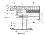
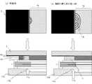
下記特許文献1の表示装置の構成を図24に示す。従来技術の表示装置は、透明カバープレート21と透明カバープレート裏面の表示領域外周に遮光性を有する黒色のインクを印刷した遮光性印刷22と、TFT(Thin Film Transistor)基板23、CF(Color Filter)基板24、位相差補正フィルム25、偏光板・光学フィルム26、ドライバIC27にて構成した表示装置と、透明カバープレートと表示装置を全面貼り合せする透明な光硬化型樹脂28にて構成される。 FIG. 24 shows the configuration of the display device of
光硬化型樹脂28の厚みは、30μm〜200μmの範囲で、表示装置の外周からのはみ出しは、約0.3mm以内である。遮光性印刷22と表示装置により挟まれた部分では、カバープレート上方や表示装置下方からは、硬化用の光が当たらない為、カバープレート外周の側方より光を照射し70%以上に硬化する。 The thickness of the
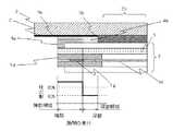
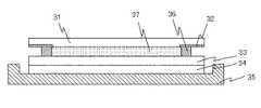
下記特許文献2の表示装置の構成を図25に示す。従来技術の表示装置は、透明カバープレート31と透明カバープレート裏面の表示領域外周に遮光性を有する黒色のインクを印刷した遮光性印刷32と、フラットパネルディスプレイ33、バックライト34及びベゼル35により構成した表示装置と、カバープレート外縁に設けたダム部36と、透明カバープレートと表示装置を全面貼り合せする透明な光硬化型樹脂37にて構成される。 FIG. 25 shows a configuration of a display device of
ダム部36は、あらかじめ透明カバープレート31に高さ150μm、幅1mmでビード状に塗布し光硬化させて形成する。光硬化型樹脂37はダム部36の内側に厚みが150μmになるように所定量塗布し、表示装置と貼り合せ、UV光等を照射してフル硬化させる。 The
特許文献1では、透明カバープレート21の遮光性印刷22と表示装置で挟まれた場所にある光硬化型樹脂28は、70%以上で一様な硬化率である。また、特許文献2では、光硬化型樹脂37はフル硬化で一様な硬化率である。 In
このように特許文献1、2では、透明カバープレートと表示装置で挟まれた場所にある光硬化型樹脂は、一様な硬化率で、高い硬化率に硬化させているため、外力により透明カバープレートが変形した際、表示領域に応力が加わって表示不良が発生する。また、光硬化型樹脂を一様な硬化率で、低い硬化率に硬化させた場合には、外力により透明カバープレートが表示装置より剥離するという課題がある。 As described above, in
また、特許文献2では、ダム部36により光硬化型樹脂37のはみ出しを防止しており、表示装置端まで樹脂が到達していない為、透明カバープレート31の端からの外力により、透明カバープレート31が表示装置より剥離しやすいという課題がある。 In
本発明は、上記問題点に鑑みてなされたものであって、その主たる目的は、外力による表示不良やカバープレートの剥離がない表示装置等の機器及びその製造方法を提供することにある。 The present invention has been made in view of the above problems, and a main object of the present invention is to provide a device such as a display device that does not cause display failure or peeling of a cover plate due to an external force, and a method of manufacturing the same.
本発明の一側面は、板状の基部とカバープレートとが硬化性樹脂によって貼合された機器であって、前記基部又は前記カバープレートの少なくとも一方の周縁に遮光部を有し、前記基部と前記カバープレートとの隙間にある前記硬化性樹脂は、前記遮光部の外周側の第1硬化性樹脂と、前記遮光部の内周側の第2硬化性樹脂と、前記遮光部の内側の透明領域の第3硬化性樹脂と、を含み、前記第2硬化性樹脂は、弾性率、硬化率又は接着力が、前記第1硬化性樹脂よりも低いことを特徴とする。 One aspect of the present invention is a device in which a plate-shaped base and a cover plate are bonded with a curable resin, and has a light-shielding portion on at least one peripheral edge of the base or the cover plate. The curable resin in the gap with the cover plate includes a first curable resin on an outer peripheral side of the light shielding unit, a second curable resin on an inner peripheral side of the light shielding unit, and a transparent resin on the inner side of the light shielding unit. And a third hardening resin in a region, wherein the second hardening resin has an elastic modulus, a hardening rate or an adhesive force lower than that of the first hardening resin.
本発明の一側面は、板状の基部とカバープレートとが硬化性樹脂によって貼合され、前記基部又は前記カバープレートの少なくとも一方の周縁に遮光部を有する機器の製造方法であって、前記基部と前記カバープレートの少なくとも一方に前記硬化性樹脂を塗布し、前記基部と前記カバープレートとを位置合わせし、貼り合せを行う貼り合せ工程と、前記カバープレートと前記基部の隙間の前記遮光部にある前記硬化性樹脂全体を硬化させる全体硬化工程と、前記カバープレートと前記基部の隙間の前記遮光部の外周側にある前記硬化性樹脂のみを硬化させる部分硬化工程と、をこの順に有し、前記遮光部の内周側の前記硬化性樹脂は、弾性率、硬化率又は接着力が、前記遮光部の外周側の前記硬化性樹脂よりも低くなるようにすることを特徴とする。 One aspect of the present invention is a method for manufacturing a device in which a plate-shaped base and a cover plate are bonded with a curable resin, and a light-shielding portion is provided on at least one peripheral edge of the base or the cover plate. And applying the curable resin to at least one of the cover plates, aligning the base and the cover plate, and performing a bonding process, and the light shielding portion in the gap between the cover plate and the base. An overall curing step of curing the entire curable resin, and a partial curing step of curing only the curable resin on the outer peripheral side of the light shielding portion in the gap between the cover plate and the base, in this order, The curable resin on the inner peripheral side of the light-shielding portion has an elastic modulus, a curing rate or an adhesive force lower than that of the curable resin on the outer peripheral side of the light-shielding portion. To.
本発明の一側面は、板状の基部とカバープレートとが硬化性樹脂によって貼合され、前記基部又は前記カバープレートの少なくとも一方の周縁に遮光部を有する機器の製造方法であって、前記基部と前記カバープレートの少なくとも一方に前記硬化性樹脂を塗布し、前記基部と前記カバープレートとを位置合わせし、貼り合せを行う貼り合せ工程と、前記カバープレートと前記基部の隙間の前記遮光部の外周側にある前記硬化性樹脂のみを硬化させる部分硬化工程と、前記カバープレートと前記基部の隙間の前記遮光部にある前記硬化性樹脂全体を硬化させる全体硬化工程と、をこの順に有し、前記遮光部の内周側の前記硬化性樹脂は、弾性率、硬化率又は接着力が、前記遮光部の外周側の前記硬化性樹脂よりも低くなるようにすることを特徴とする。 One aspect of the present invention is a method for manufacturing a device in which a plate-shaped base and a cover plate are bonded with a curable resin, and a light-shielding portion is provided on at least one peripheral edge of the base or the cover plate. And applying the curable resin to at least one of the cover plates, aligning the base and the cover plate, and performing a bonding process, and a step of bonding the light shielding portion in a gap between the cover plate and the base. A partial curing step of curing only the curable resin on the outer peripheral side, and an overall curing step of curing the entire curable resin in the light shielding portion in the gap between the cover plate and the base, in this order, The curable resin on the inner peripheral side of the light-shielding portion has an elastic modulus, a curing rate or an adhesive force lower than that of the curable resin on the outer peripheral side of the light-shielding portion. To.
本発明によれば、遮光部を有するカバープレートと画像表示領域を有する基部を硬化性樹脂によって全面貼り合せを行う表示装置において、外力によるカバープレートの剥離を防止するとともに、外力によりカバープレートが変形した際の表示領域への応力を軽減し、表示不良を軽減することができる。 According to the present invention, in a display device in which a cover plate having a light-shielding portion and a base having an image display area are entirely bonded with a curable resin, peeling of the cover plate due to external force is prevented, and the cover plate is deformed by external force. In this case, the stress on the display area when the display is performed can be reduced, and display defects can be reduced.
背景技術で示したように、光で硬化可能な光学弾性樹脂を用いてカバープレートと表示装置を接着する構造が用いられているが、従来は、カバープレートと表示装置で挟まれた場所にある光硬化型樹脂を、一様な高い硬化率で硬化させているため、外力によりカバープレートが変形した際、表示領域に応力が加わって表示不良が発生する。また、光硬化型樹脂を一様な低い硬化率で硬化させた場合には、外力によりカバープレートが表示装置より剥離するという課題がある。また、特許文献2のように、ダム部36により光硬化型樹脂37のはみ出しを防止した場合には、カバープレート端からの外力により、カバープレートが表示装置から剥離しやすいという課題もある。 As shown in the background art, a structure in which a cover plate and a display device are bonded using an optical elastic resin curable by light is used, but conventionally, a structure is used in a place sandwiched between the cover plate and the display device. Since the photocurable resin is cured at a uniform high curing rate, when the cover plate is deformed by an external force, stress is applied to the display area, and display failure occurs. Further, when the photocurable resin is cured at a uniform low curing rate, there is a problem that the cover plate is peeled off from the display device by an external force. Further, in the case where the protrusion of the
そこで、本発明の一実施の形態では、遮光部を有するカバープレートと表示領域を有する基部との間に硬化性樹脂を介在させて全面貼り合せを行う表示装置などの機器において、硬化性樹脂を一様な高い硬化率で硬化させるのではなく、カバープレートの遮光部と表示装置で挟まれた場所にある硬化性樹脂の硬化率を、遮光部の内周近傍(深部)が非流動状態になるよう硬化させ、遮光部の内周近傍(深部)の硬化率が、遮光部外周(端部)の硬化率より低くなるように硬化させる。これにより、外力によりカバープレートが変形した際の表示領域への応力を軽減し、表示不良を軽減すると共に、外力によるカバープレートの剥離を抑制する。以下、図面を参照して詳細に説明する。 Therefore, in one embodiment of the present invention, in a device such as a display device in which a curable resin is interposed between a cover plate having a light-shielding portion and a base having a display region and the entire surface is bonded, the curable resin is used. Instead of curing at a uniform high curing rate, the curing rate of the curable resin between the light-shielding part of the cover plate and the display device is changed to a non-fluid state near the inner circumference (deep part) of the light-shielding part. Curing is performed so that the curing rate near the inner periphery (deep portion) of the light shielding portion is lower than the curing ratio at the outer periphery (end portion) of the light shielding portion. This reduces stress on the display area when the cover plate is deformed by external force, reduces display defects, and suppresses peeling of the cover plate due to external force. The details will be described below with reference to the drawings.
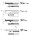
まず、本発明の実施例1に係る機器及びその製造方法について、図1乃至図16を参照して説明する。本実施例では、本発明の構造を、画像表示領域に液晶パネル1を用いた基部と、遮光部3を有するカバープレート2と、硬化性樹脂4に光硬化型樹脂を用い、基部とカバープレート2を光硬化型樹脂にて全面貼り合せした表示装置に適用した場合の例を示す。以下に、本発明の実施例1の構成について、図1、図2を参照して説明する。 First, an apparatus according to a first embodiment of the present invention and a method for manufacturing the same will be described with reference to FIGS. In the present embodiment, the structure of the present invention is modified by using a base using the
基部は、フラットパネルディスプレイ、液晶表示装置、液晶パネル、LCD(Liquid Crystal Display)モジュール等の画像表示装置であり、本実施例では液晶パネルにて説明する。 The base unit is an image display device such as a flat panel display, a liquid crystal display device, a liquid crystal panel, and an LCD (Liquid Crystal Display) module. In this embodiment, the description will be made using the liquid crystal panel.
基部は、液晶パネル1であり、画像を表示する表示領域1eと表示領域1eの周囲で表示信号を供給するための配線領域1dを有する。表示領域1eは、TFT素子、RGB(赤、緑、青画素)、BM(ブラックマトリクス)パターンが形成(図示せず)され、表示信号により画像を表示する。配線領域1dは、TFT素子に表示信号を供給する配線(図示せず)があり、配線は金属膜等を用いる為、光を透過しない。また、配線領域1dには遮光膜を形成して図示していないバックライトからの光を遮光する。 The base is a
基部の液晶パネル1はTFT素子等がパターンニングされたTFT基板1b、RGB、BMパターン等がパターンニングされたカラーフィルタ基板1a、TFT基板1bとカラーフィルタ基板1aとを接合すると共に、その内側に任意の隙間を設けるシール1g、TFT基板1bとカラーフィルタ基板1aの隙間に充填された液晶剤1f、表面及び裏面に貼合される偏光板・光学補償フィルム1c等により構成される。 The base
遮光部3を有するカバープレート2は、透明なガラス、強化ガラスやアクリル板、PET板等のプラスチックを用いた基板やそれらの複合基板で、カバープレート2と基部を貼合した際に、基部の表示領域1eに相当する部位(透明領域2b)以外の外周部(周縁)には遮光性を有する黒インクで形成した遮光部3により遮光した帯状の遮光領域2aを有する。なお、本実施例の遮光部3は、黒インクを用いて形成しているが、遮光性を有する材料(たとえば色インク)や遮光性を有する表面処理(たとえば反射膜成膜)を用いて遮光部3を設けることができる。 The
基部と遮光部3を有するカバープレート2の貼合に用いる硬化性樹脂4は、光硬化型樹脂、熱硬化型樹脂、湿気硬化型樹脂や、光硬化型樹脂、熱硬化型樹脂、湿気硬化型樹脂などの硬化機能を複合して有するハイブリット硬化型樹脂等の樹脂があるが、本実施例では光硬化型樹脂を用いた例で説明する。 The
カバープレート2と基部との隙間の光硬化型樹脂は、光により硬化する樹脂であり、遮光部3の外周側にある硬化性樹脂(請求項における第1硬化性樹脂)と、遮光部3の内周側(内周近傍)にある硬化性樹脂(請求項における第2硬化性樹脂)と、遮光部3の内側の透明領域2bにある硬化性樹脂(請求項における第3硬化性樹脂)とを含む。これらの内、基部の表示領域1eに近い、遮光部3の内周近傍3b(深部)にある深部領域硬化性樹脂4bの硬化後の硬化率と、遮光部3の外周側3a(端部)にある端部領域硬化性樹脂4aの硬化後の硬化率が異なり、深部領域硬化性樹脂4bの硬化後の硬化率が、端部領域硬化性樹脂4aの硬化後の硬化率より低くなるよう硬化させる。隙間の硬化性樹脂4を硬化する方法は、後述する製造方法にて説明する。 The photo-curable resin in the gap between the
図2に示すように、基部の表示領域1eに近い深部領域硬化性樹脂4bの硬化後の硬化率は、60%程度で非流動(非流動の定義は後述する。)の硬化状態となり、端部領域硬化性樹脂4aの硬化後の硬化率は、80%以上の硬化状態とすることが好ましい。なお、本実施例では、遮光部3の内周近傍3bを深部、遮光部3の外周側3aを端部とし、硬化率が端部から深部に向かってなだらかに減少するよう図示しているが、理想的な硬化状態は、図3に示すように、端部と深部の硬化率が階段状に変化をするものである。 As shown in FIG. 2, the hardening rate of the deep
階段状の硬化率を得るには、硬化用のUV光を2種類以上の波長と波長毎の照度を選択的に制御することで実現可能である。例えば遮光部3の外周側3aにある硬化性樹脂4の端より10mmまでを端部領域硬化性樹脂4a、基部の表示領域1e側で遮光部3の内周近傍3bにある硬化性樹脂4の端より20mmまでを深部領域硬化性樹脂4bにする場合、図4(a)に示すように、硬化性樹脂4の硬化条件を波長と波長毎の照度にて確認しておき、その結果を用いて、深部領域硬化性樹脂4bの硬化に有効な長波長(例えば400nm)を照度:中の条件で照射して端部領域硬化性樹脂4aを硬化し、端部領域硬化性樹脂4aの硬化に有効な短波長(例えば360nm)を照度:高の条件で照射して端部領域硬化性樹脂4aを硬化することで図4(b)に示すような階段状の硬化が実現可能である。 A stepwise curing rate can be achieved by selectively controlling two or more wavelengths of the curing UV light and the illuminance for each wavelength. For example, up to 10 mm from the end of the
なお、図5に示すように、カバープレート2の遮光部3と基部の配線領域1dの隙間の光硬化型樹脂を、基部の端部まで充填することで、基部の液晶パネル1表面及び裏面に貼り付けている偏光板・光学補償フィルム1cの劣化を抑制することが可能である。 In addition, as shown in FIG. 5, by filling the light-curing resin in the gap between the light-shielding
また、図5に示すように、カバープレート2の遮光部3は、カバープレート2の外周端まで設けず、表示領域1e上にある透明領域2bから、カバープレート2の外周端の途中までを遮光する場合も、カバープレート2の遮光部3と基部の隙間にある硬化性樹脂4の深部領域硬化性樹脂4bの硬化後の硬化率が、端部領域硬化性樹脂4aの硬化後の硬化率より低くなるよう硬化させることが可能である。 As shown in FIG. 5, the light-shielding
また、液晶パネルでは、TFT基板1bとカラーフィルタ基板1aの隙間の、シール1gにより区画された領域に充填される液晶剤1fは流動状態であり、液晶剤1fが充填された部分に外力が加わると、隙間が変動し表示不良になりやすい。そこで、カバープレート2の遮光部3の内周側端部からシール1gの内周側までの領域に上記の深部領域硬化性樹脂4bが配置され、遮光部3の外周側からシール1gの内周側までの領域に上記の端部領域硬化性樹脂4aが配置される。図6に示すように、この外力を軽減する為に、カバープレート2の遮光部3と基部の配線領域1dの隙間の硬化性樹脂4のうち、深部領域硬化性樹脂4bの硬化後の硬化率を低くすることもできる。このようにすることで、基部の液晶パネル1が外力により表示異常となることを抑制することが可能である。なお、硬化性樹脂4の深部領域硬化性樹脂4bの硬化後の硬化率より、端部領域硬化性樹脂4aの硬化後の硬化率が高くなるように硬化させる位置は、表示領域1eの周囲の一部に適用することも可能である。 Further, in the liquid crystal panel, the
以上では、基部が液晶パネル1で、カバープレート2が遮光部3を有するプレートの場合について説明したが、基部またはカバープレート2にはタッチセンサー5を有する基板を用い、タッチパネル等の入力機能を付加した構造であってもよい。例えば、図7に示すように、カバープレート2にタッチセンサー5を付加した、タッチセンサー付きカバープレート6を用いた構造としたり、図8に示すように、基部の液晶パネル1にタッチセンサー5を付加した、タッチセンサー付き液晶パネル7を用いた構造としたりすることができる。 In the above, the case where the base is the
また、以上では、基部及びカバープレート2の両方に遮光性を有する場合について説明したが、基部またはカバープレート2のいずれか片方に遮光性を有する構造であっても良い。例えば、図9に示すように、基部に遮光性がないタッチセンサー5を用いた構造としたり、図10に示すように、遮光性がないカバープレート2を用いた構造としたりすることができる。 Further, in the above, the case where both the base and the
以上説明した構造の効果を確認するために、本願出願人は、光硬化型樹脂を一様に硬化させた際の、硬化率と外力によるカバープレートに対する接着強度を確認した。その結果を下記の表1に示す。 In order to confirm the effects of the structure described above, the present applicant has confirmed the adhesive strength to the cover plate due to the curing rate and external force when the photocurable resin is uniformly cured. The results are shown in Table 1 below.
表1における光硬化型樹脂の硬化率に関しては、照射前の硬化性樹脂に含まれる樹脂組成物と、照射後の硬化性樹脂に含まれる、光反応する硬化成分(例えばビニル基C=C)を、FT−IR等により、それぞれ抽出し、照射前の硬化性樹脂に含まれる樹脂組成物より抽出したピーク強度:P0と照射後の硬化成分より抽出したピーク強度:P1を求め、次式1により算出した。Regarding the curing rate of the photo-curable resin in Table 1, the resin composition contained in the curable resin before irradiation and the photo-reactive curing component (for example, vinyl group C = C) contained in the curable resin after irradiation. and by FT-IR, etc., respectively extracted, the peak intensities were extracted from the resin composition contained in the curable resin before irradiation: P0 and the peak intensity extracted from curing component after irradiation: seeking P1, the following It was calculated by
硬化率(%)={(P0−P1)/P0}×100 … (1)Hardening rate(%) = {(P 0 -P 1) / P 0} × 100 ... (1)
硬化率が80%以上であれば、接着強度0.24N/mm2以上を得ることができ、硬化率60%以下では接着強度0.15N/mm2以下であり、硬化率80%は硬化率60%に対して1.6倍の強度を得ることができた。接着強度がさらに必要な場合は、硬化率を高めることで対応が可能であり、硬化率100%程度では0.32N/mm2以上の強度を得ることができた。When the curing rate is 80% or more, an adhesive strength of 0.24 N / mm2 or more can be obtained. When the curing rate is 60% or less, the adhesive strength is 0.15 N / mm2 or less. 1.6 times the strength was obtained for 60%. If further adhesive strength is required, it is possible to cope with the problem by increasing the curing rate. At a curing rate of about 100%, a strength of 0.32 N / mm2 or more could be obtained.
表1における外部応力による外観状態は、端部の剥離、表示領域の気泡及び液漏れの有無により判断し、気泡が発生し、液漏れも出る場合は“×”、剥離するが表示領域の気泡、液漏れがない場合は“△”、剥離がなく気泡、液漏れもない場合は“○”とした。 The appearance state due to the external stress in Table 1 is determined based on the presence or absence of peeling of the end portion, bubbles in the display area and liquid leakage. When there was no liquid leakage, "△" was given, and when there was no peeling and no bubbles and no liquid leakage, "“ "was given.

また、本願出願人は、光硬化型樹脂を一様に硬化させた際の、硬化率と弾性率と外力による表示への影響について確認した。その結果を下記の表2に示す。 In addition, the applicant of the present application has confirmed the effects of the curing rate, the elastic modulus, and the external force on the display when the photocurable resin is uniformly cured. The results are shown in Table 2 below.
表2では、光硬化型樹脂の状態として、使用や保管する環境温度(例えば25℃程度)や設置状態(例えば縦置き設置)を一定にした場合において、光硬化型樹脂が未硬化や硬化率が低い状態で隙間より流れ出てくる状態を“流動:×”、硬化反応が進み隙間より流れ出ない状態を“非流動:○”とした。 In Table 2, when the environmental temperature (for example, about 25 ° C.) for use or storage and the installation state (for example, vertical installation) are constant as the state of the photocurable resin, the photocurable resin is uncured or hardened. The state in which the resin flowed out of the gap in a low state was "flow: x", and the state in which the curing reaction proceeded and did not flow out of the gap was "non-flow: o".
また、外部応力による表示状態は、押しムラ等が顕著に発生する場合は“×”、軽微な押しムラ等が発生する場合は“△”、押しムラ等の発生がなく良好な場合は“○”とした。 The display state due to the external stress is “×” when the press unevenness or the like occurs remarkably, “△” when the slight press unevenness or the like occurs, and “○” when the press unevenness or the like is good without any uneven press. "
硬化率80%以上であれば、非流動状態で弾性率7KPa以上となり、硬化率60%では、非流動化状態で弾性率は5KPa以下であるが、硬化率50%では、流動状態(弾性率は1KPa以下)となり、光硬化型樹脂は基部とカバープレートの隙間より流れ出す。また、硬化率80%以上に硬化すると、外部応力により基部に用いている液晶表示装置の表示状態は押しムラにより悪化し、硬化率60%以下にて押しムラは見えにくくなる。 When the curing rate is 80% or more, the elasticity becomes 7 KPa or more in a non-fluidized state, and when the curing rate is 60%, the elasticity is 5 KPa or less in a non-fluidized state. Is 1 KPa or less), and the photocurable resin flows out of the gap between the base and the cover plate. When the curing rate is 80% or more, the display state of the liquid crystal display device used for the base is deteriorated due to the uneven pressing due to external stress, and when the curing rate is 60% or less, the uneven pressing becomes difficult to see.
本実施例の図3のように、カバープレート2の遮光部3と基部の配線領域1dの隙間の光硬化型樹脂の深部を硬化率60%程度で非流動の硬化状態とし、端部を硬化率80%以上の硬化状態とした場合、接着強度は0.31N/mm2で、外部応力による表示状態は良好な結果を得た。また、上記光硬化型樹脂の深部の硬化率は5KPa以下で、外部応力による表示状態は良好な結果を得た。As shown in FIG. 3 of the present embodiment, the deep portion of the photo-curable resin in the gap between the light-shielding
なお、本実施例では、硬化性樹脂4の状態を硬化率にて規定する構成を示したが、一般に硬化率が高い場合、弾性率及び接着強度は高く、硬化率が低い場合、弾性率及び接着強度は低い為、弾性率では、端部領域硬化性樹脂4aの硬化後の弾性率より、深部領域硬化性樹脂4bの硬化後の弾性率が低くなるよう硬化し、接着強度では、深部領域硬化性樹脂4bの硬化後の接着強度より、端部領域硬化性樹脂4aの硬化後の接着強度が高くなる状態に硬化している。 In the present embodiment, the configuration in which the state of the
上記表1、表2は、光硬化型樹脂の評価結果であるが、本実施例の硬化性樹脂4は光硬化型樹脂に限定されず、他の熱硬化型樹脂、ハイブリット硬化型樹脂等の硬化性樹脂4においても、表に示したような特性に基づき硬化状態を制御することで、本実施例のような構成を実現することができる。 Tables 1 and 2 above show the evaluation results of the photo-curable resin. However, the
次に、本発明の構造を、画像表示領域に液晶パネル1を用いた基部と、遮光部3を有するカバープレート2と、を光硬化型樹脂である硬化性樹脂4にて全面貼り合せした表示装置に適用した場合の製造方法について、図11を参照して説明する。 Next, the structure of the present invention is applied to a display in which the base using the
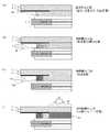
まず、図11(a)に示すように、基部である液晶パネル1と遮光部3を有するカバープレート2の少なくとも一方に光硬化型樹脂を塗布し、基部とカバープレート2を位置合わせし、未硬化の硬化性樹脂4dにて貼り合せを行う。貼合後に次工程に搬送する際の位置ずれ等を防止する為に、光硬化型樹脂を部分的に仮硬化しても構わない。 First, as shown in FIG. 11A, a photocurable resin is applied to at least one of the
光硬化型樹脂を塗布する方法は、特に限定されず、例えば、ディスペンサーを用いる方法、コーターを用いる方法、印刷を用いる方法等がある。これらの中では、塗布量の制御及び貼合時の気泡混入を防止する点からディスペンサーを用いる方法が好ましい。 The method of applying the photocurable resin is not particularly limited, and examples thereof include a method using a dispenser, a method using a coater, and a method using printing. Among these, a method using a dispenser is preferable from the viewpoint of controlling the amount of application and preventing air bubbles from entering during bonding.
また、基部とカバープレート2を位置合わせする方法は、特に限定されず、例えば、外形基準にて位置決めする方法、カバープレート2の遮光部パターンと基部の液晶パネル1に設けた貼合用位置決めマーク(図示しない)とを画像処理して位置決めする画像処理位置決め方法等がある。これらの中では、位置決め精度の点から画像処理位置決め方法が好ましい。 The method of positioning the base and the
また、基部とカバープレート2を貼合する方法は、特に限定されず、例えば、貼合環境では、常圧下で貼合する方法、真空下で貼合する方法があり、貼合方式としてローラーにて貼合する方法、平行平板にて貼合する方法等がある。これらの中では、貼合時の気泡を防止する観点から、真空下で平行平板にて貼合する方法が好ましい。 The method of bonding the base and the
次に、図11(b)に示すように、カバープレート2の上方または基部の下方よりUV光8を照射し、カバープレート2の透明領域2bの下部にある光硬化型樹脂を硬化させる(硬化した硬化性樹脂4e)。図ではカバープレート2の上方より照射した例を示す。 Next, as shown in FIG. 11B,
カバープレート2の透明領域2bにある光硬化型樹脂を硬化する方法は、特に限定されず、例えば、貼合したカバープレート2と基部とを、カバープレート2を上側にして置き、カバープレート2上方に配したUVランプにて一括照射する方法、スポットUVランプにて均一に走査して照射する方法、カバープレート2と基部とを、カバープレート2を下側にして置き、コンベアで搬送しながらカバープレート2下方に配したUVランプにて照射する方法等がある。これらの中では、照射による硬化状態の均一性の観点から、コンベアで搬送しながらUVランプにて照射する方法が好ましい。 The method of curing the photocurable resin in the
その次に、図11(c)に示すように、カバープレート2の遮光部3と基部の配線領域1dの隙間の深部まで光硬化型樹脂をUV光8により硬化させる(60%程度硬化した硬化性樹脂4f)。 Then, as shown in FIG. 11 (c), the photocurable resin is cured by
カバープレート2と基部の隙間の深部にある光硬化性樹脂を硬化させる方法は、特に限定されず、例えば、400nm程度の長波長光を照射可能なLED光源を用いる方法、光線を平行光に調光可能な光学レンズ等を用いる方法、光源を隙間に対して平行な位置より照射する方法等がある。本実施例では、これらを組み合わせて、隙間の深部に光を到達させ隙間深部を安定して硬化させる点から、長波長光を照射可能な光源と光線を平行光に調光可能な光学レンズを用い隙間に平行な位置より照射する方法が好ましい。 The method of curing the photocurable resin in the deep part of the gap between the
その次に、図11(d)に示すように、カバープレート2の遮光部3と基部の配線領域1dの隙間の端部にある光硬化型樹脂をUV光8により硬化させる(80%以上硬化した硬化性樹脂4g)。なお、カバープレート2の遮光部3と基部の配線領域1dの隙間の端部にある光硬化型樹脂は、図11(c)のUV光8(400nm程度の長波長のUV光)によってある程度硬化しているため、本工程のUV光照射によって80%以上硬化するように、UV光8の波長及び照度を調整すればよい。 Then, as shown in FIG. 11D, the photocurable resin at the end of the gap between the light-shielding
カバープレート2と基部の隙間の端部にある光硬化性樹脂を硬化させる方法は、特に限定されず、例えば、360nm程度の短波長光を照射可能なLED光源を用いる方法、光線をスポット状に集光可能な光学レンズ等を用いる方法、光源を隙間の斜め下方より照射する等がある。本実施例では、これらを組み合わせて、隙間の端部に光を集中させ隙間端部を安定して硬化させる点から、短波長光を照射可能な光源と光線をスポット状に調光可能な光学レンズを用い隙間の斜め下方より照射する方法が好ましい。 The method for curing the photocurable resin at the end of the gap between the
次に、本実施例の表示装置の他の製造方法について、図12を参照して説明する。 Next, another method for manufacturing the display device of this embodiment will be described with reference to FIG.
まず、図12(a)に示すように、基部である液晶パネル1と遮光部3を有するカバープレート2の少なくとも一方に光硬化型樹脂を塗布し、基部とカバープレート2を位置合わせし、貼り合せを行う。次に、図12(b)に示すように、カバープレート2の遮光部3と基部の隙間の深部まで光硬化型樹脂をUV光8により硬化させる(60%程度硬化した硬化性樹脂4f)。この工程は、上記と同様に、400nm程度の長波長光を照射可能な光源と光線を平行光に調光可能な光学レンズを用い隙間に平行な位置より照射する方法を用いて行うことができる。その次に、図12(c)に示すように、カバープレート2の遮光部3と基部の隙間の端部にある光硬化型樹脂をUV光8により硬化させる(80%以上硬化した硬化性樹脂4g)。この工程も、上記と同様に、360nm程度の短波長光を照射可能な光源と光線をスポット状に調光可能な光学レンズを用い隙間の斜め下方より照射する方法を用いて行うことができる。なお、上記と同様に、カバープレート2の遮光部3と基部の隙間の端部にある光硬化型樹脂は図12(b)のUV光8によってある程度硬化しているため、本工程のUV光照射によって80%以上硬化するように、UV光8の波長及び照度を調整すればよい。その次に、図12(d)に示すように、カバープレート2の上方または基部の下方(図ではカバープレート2の上方)よりUV光8を照射し、カバープレート2の透明領域2bの下部にある光硬化型樹脂を硬化させる(硬化した硬化性樹脂4e)。この工程も、上記と同様に、コンベアで搬送しながらUVランプにて照射する方法などを用いて行うことができる。 First, as shown in FIG. 12A, a photocurable resin is applied to at least one of the
この方法によれば、図12(a)、図12(b)及び図12(c)の工程を同一の装置内に組み込むことが可能であり、また、図12(a)にて貼合した後、図12(b)を同一装置にて処理することで、貼合後に次工程に搬送する際の位置ずれ等を防止するために必要な仮硬化を兼ねることが可能である。 According to this method, the steps of FIG. 12A, FIG. 12B and FIG. 12C can be incorporated in the same device, and the steps of FIG. After that, by processing in FIG. 12 (b) using the same apparatus, it is possible to also serve as temporary curing necessary for preventing displacement or the like when transporting to the next step after bonding.
次に、硬化性樹脂4として熱硬化型樹脂を用いる場合の表示装置の製造方法について、図13を参照して説明する。 Next, a method of manufacturing a display device when a thermosetting resin is used as the
まず、図13(a)に示すように、基部である液晶パネル1と遮光部3を有するカバープレート2の少なくとも一方に熱硬化型樹脂を塗布し、基部とカバープレート2を位置合わせし、貼り合せを行う。次に、図13(b)に示すように、カバープレート2の遮光部3と基部の隙間の深部まで熱硬化型樹脂を遠赤外線9bにて硬化させる(60%程度硬化した硬化性樹脂4f)。その次に、図13(c)に示すように、カバープレート2の遮光部と基部の隙間の端部にある熱硬化型樹脂を赤外線9aにて硬化させる(80%以上硬化した硬化性樹脂4g)。なお、上記と同様に、カバープレート2の遮光部3と基部の隙間の端部にある光硬化型樹脂は図13(b)の遠赤外線9bによってある程度硬化しているため、本工程の赤外線照射によって80%以上硬化するように、赤外線9aの波長及び照度を調整すればよい。その次に、図13(d)に示すように、カバープレート2の上方または基部の下方(図ではカバープレート2の上方)より赤外線9aを照射し、カバープレート2の透明領域2bにある熱硬化型樹脂を硬化させる。 First, as shown in FIG. 13A, a thermosetting resin is applied to at least one of the
この方法によれば、硬化性樹脂4として熱硬化型樹脂を用いた場合でも、前述した図1から図10の構成を実現することが可能である。 According to this method, even when a thermosetting resin is used as the
さらに、硬化性樹脂4として湿気硬化機能を有するハイブリット硬化型樹脂を用いる場合の表示装置の製造方法について、図14を参照して説明する。 Further, a method of manufacturing a display device when a hybrid curable resin having a moisture curable function is used as the
ハイブリット硬化型樹脂は、光硬化型や熱硬化型等の硬化機能に湿気硬化機能を付加した硬化性樹脂4であり、光硬化型と湿気硬化型の機能を有するハイブリット硬化型樹脂を用いる場合、図11、図12の製造方法に湿気硬化工程を組み合わせることで表示装置の製造が可能である。 The hybrid curable resin is a
例えば、図14(a)に示すように、基部である液晶パネル1と遮光部3を有するカバープレート2の少なくとも一方にハイブリット硬化型樹脂を塗布し、基部とカバープレート2を位置合わせし、貼り合せを行う。次に、図14(b)に示すように、カバープレート2の遮光部3と基部の隙間の深部までハイブリット硬化型樹脂をUV光8にて硬化させる。次に、図14(c)に示すように、カバープレート2の遮光部3と基部の隙間の端部にあるハイブリット硬化型樹脂に湿気10を加え硬化させる。その次に、図14(d)に示すように、前記カバープレート2の上方または基部の下方(図ではカバープレート2の上方)よりUV光8を照射し、カバープレート2の透明領域2bにあるハイブリット硬化型樹脂を硬化させる。 For example, as shown in FIG. 14A, a hybrid curing resin is applied to at least one of the
この方法によれば、硬化性樹脂4としてハイブリット硬化型樹脂を用いた場合でも、前述した図1から図6の構成を実現することが可能である。 According to this method, even when a hybrid curable resin is used as the
また、硬化性樹脂4として熱硬化型と湿気硬化型の機能を有するハイブリット硬化型樹脂についても、図13と図14の製造方法を組み合わせることで、前述した図1から図10の構成を実現することが可能である。 Also, for the hybrid curable resin having the thermosetting and moisture curable functions as the
なお、図11乃至図14では、カバープレート2の遮光部3と基部の隙間の深部の硬化性樹脂まで(すなわち、遮光部3にある硬化性樹脂全体)を硬化させた後、カバープレート2の遮光部3と基部の隙間の端部にある硬化性樹脂を硬化させたが、端部にある硬化性樹脂を先に硬化させた後、深部の硬化性樹脂まで硬化させることも可能である。その場合、端部にある硬化性樹脂は後の硬化工程によって更に硬化されるため、先の硬化工程では、後の硬化工程による硬化を考慮して硬化条件を調整することが好ましい。 In FIGS. 11 to 14, after the hardening resin at the deep portion of the gap between the light-shielding
次に、本発明の実施例1の動作について、図15、図16を参照して説明する。 Next, the operation of the first embodiment of the present invention will be described with reference to FIGS.
図15に示すように、貼合したカバープレート2と基部とのいずれか片方(本動作説明ではカバープレート2)に、引きはがす外力11が加わったとする。 As shown in FIG. 15, it is assumed that an
図15(a)に示すように、引きはがす外力11は、端部領域硬化性樹脂4aに加わるが、端部領域硬化性樹脂4aは十分に硬化している為、硬化性樹脂4の接着強度によって剥離しにくい。また、剥離しても深部領域硬化性樹脂4bは非流動状態である為、深部領域硬化性樹脂4bが隙間より流れ出ず、カバープレート2、基部及びその周辺環境を汚染しない。 As shown in FIG. 15A, the
一方、図15(b)に示すように、隙間の硬化性樹脂4の硬化後の硬化率が一様に低いと、カバープレート2と基部とが硬化性樹脂4より剥離13し、表示領域1e内に気泡12が発生し、更に隙間内部の硬化が不十分であると、硬化性樹脂4の未硬化部分が流れ出し、カバープレート2、基部及びその周辺環境を汚染する。 On the other hand, as shown in FIG. 15B, if the curing rate of the
図16に示すように、貼合したカバープレート2と基部とのいずれか片方(本動作説明ではカバープレート2)に、タッチ操作等により押しつぶす外力11が加わったとする。 As shown in FIG. 16, it is assumed that an
図16(a)に示すように、押しつぶす外力11は、隙間の深部領域硬化性樹脂4bにも加わるが、深部領域硬化性樹脂4bは十分に柔らかい為、深部領域硬化性樹脂4bが応力を吸収し応力11aは軽減する。 As shown in FIG. 16A, the crushing
一方、図16(b)に示すように、深部領域硬化性樹脂4bから液晶パネル1に伝わった応力は、液晶パネル1端部を受けている基板受け15bを有するバックライトシャーシ15aに伝わり、液晶パネル1とバックライトシャーシ15aの接した個所に集中し基部への応力11aが液晶パネル1にかかる。 On the other hand, as shown in FIG. 16B, the stress transmitted from the deep
ここで、バックライトシャーシ15aの基板受け15bから集中的に加わった応力11aは、液晶パネル1の隙間の高さを変化させるが、図16(a)の構造では、応力11aは深部領域硬化性樹脂4bに吸収されて小さくなるため、軽微な波紋状の表示不良14を発生させるに過ぎない。一方、図16(b)のように、隙間の硬化性樹脂4の硬化後の硬化率が一様に高く、弾性率が高いと、押しつぶす外力11が吸収されず、バックライトシャーシ15aの基板受け15bから集中的に加わった応力11aは、液晶パネル1の隙間の高さを大きく変化させ、波紋状の表示不良14を発生させる。 Here, the stress 11a intensively applied from the
以上説明したように、本実施例では、端部領域硬化性樹脂4aの硬化後の硬化率、弾性率、接着強度を相対的に高くしているため、引きはがす外力11によりカバープレート2と基部とが硬化性樹脂4より剥離しにくく、仮に引きはがす外力11によりカバープレート2と基部とが硬化性樹脂4より剥離したとしても、硬化性樹脂4が隙間より流れ出ず、カバープレート2、基部及びその周辺環境の汚染を防止できるという効果がある。また、本実施例では、深部領域硬化性樹脂4bの硬化後の硬化率、弾性率、接着強度を相対的に低くしているため、押しつぶす外力11による表示不良が発生しにくいという効果がある。 As described above, in the present embodiment, since the curing rate, the elastic modulus, and the adhesive strength after curing of the end region
次に、本発明の第2の実施例に係る表示装置及びその製造方法について説明する。本実施例では、本発明の構造を、画像表示領域にLCDモジュール15を用いた基部と、遮光部3を有するカバープレート2と、硬化性樹脂4に光硬化型樹脂を用い、基部とカバープレート2を光硬化型樹脂にて全面貼り合せした表示装置に適用した場合の例を示す。以下に、本発明の実施例2の構成について、図17、図18を参照して説明する。 Next, a display device and a method of manufacturing the same according to a second embodiment of the present invention will be described. In the present embodiment, the structure of the present invention is described by using a base using an
基部は、LCDモジュール15であり、画像を表示する液晶パネル1と、液晶パネル1を搭載し、下方に表示用の光源及び表示信号を供給するバックライトシャーシ15aと、液晶パネル1とバックライトシャーシ15aを保護する為の金属フレーム15cとを有する。なお、液晶パネル1の構成は、実施例1と同様であるので、説明は省略する。 The base is an
図17に示すように、LCDモジュール15の金属フレーム15cは遮光性を有する金属板等を用いたフレームであり、液晶パネル1の配線領域1d及びバックライトシャーシ15aの外周部を覆うように配置し、液晶パネル1の表示領域1eは開口する。 As shown in FIG. 17, the metal frame 15c of the
基部と遮光部3を有するカバープレート2の貼合に用いる硬化性樹脂4は、光硬化型樹脂を用いる。光硬化型樹脂は、金属フレーム15cの外周端部まで充填する。カバープレート2の遮光部3と基部の金属フレーム15cの隙間の光硬化型樹脂は、光により硬化し、遮光部3の内周近傍3b(深部)にある深部領域硬化性樹脂4bの硬化後の硬化率(又は弾性率や接着強度)と、遮光部3の外周側3a(端部)にある端部領域硬化性樹脂4aの硬化後の硬化率(又は弾性率や接着強度)が異なり、深部領域硬化性樹脂4bの硬化後の硬化率(又は弾性率や接着強度)が、端部領域硬化性樹脂4aの硬化後の硬化率(又は弾性率や接着強度)より低くなるように硬化させる。 As the
例えば、図18に示すように、基部の表示領域1eに近い、遮光部3の内周近傍3bにある深部領域硬化性樹脂4bの硬化後の硬化率は、60%程度で非流動の硬化状態となり、遮光部3の外周側3aにある端部領域硬化性樹脂4aの硬化後の硬化率は、80%以上の硬化状態とすることが好ましい。 For example, as shown in FIG. 18, the hardening rate after hardening of the deep
本実施例の構成において、貼合したカバープレート2と基部とのいずれか片方に、タッチ操作等により押しつぶす外力が加わる場合の動作(図16の動作)は、実施例1と同じである。 In the configuration of the present embodiment, the operation (the operation in FIG. 16) when an external force for crushing is applied to one of the bonded
貼合したカバープレート2と基部とのいずれか片方に、引きはがす外力11が加わった場合の動作(図15の動作)は、十分に硬化している端部領域硬化性樹脂4aの接着強度によって剥離しにくくなると共に、カバープレート2の遮光部3と基部の金属フレーム15cの隙間の光硬化型樹脂を金属フレーム15cの端部まで充填する為、硬化性樹脂4がカバープレート2と金属フレーム15cに接触する面積が増し、硬化率が高い領域を増すことができ、接着強度を増すことができる。 The operation when the peeling
このように、本実施例では、実施例1の効果に加え、更にカバープレート2と基部が外力11により剥離しにくいという効果がある。 As described above, in the present embodiment, in addition to the effect of the first embodiment, there is an effect that the
次に、本発明の第3の実施例に係る表示装置及びその製造方法について説明する。本実施例では、実施例1の構成に対して、更に、基部とカバープレート2の隙間にギャップ形成材16を配置し、基部とカバープレート2を光硬化型樹脂にて全面貼り合せした表示装置に適用した場合の例を示す。 Next, a display device and a method of manufacturing the same according to a third embodiment of the present invention will be described. In the present embodiment, a display device in which a
以下に、本発明の実施例3の構成について、図19、図20を参照して説明する。基部とカバープレート2は、実施例1と同様であるので、説明は省略する。 Hereinafter, the configuration of the third embodiment of the present invention will be described with reference to FIGS. 19 and 20. Since the base and the
図19に示すように、ギャップ形成材16は、基部とカバープレート2の隙間で、表示領域1eの周囲(本実施例では、液晶パネル1のシール1gの上部)に設けられており、基部とカバープレート2の隙間が所定の高さになるような厚みを有する。具体的には、カバープレート2と基部の高さは、0.1mm以上が好ましく、0.5mm程度で硬化性樹脂4の弾性によって外力によるカバープレート2と基部の剥離が発生しにくくなり、1mm程度になると樹脂の使用量が多くコスト増の要因となることから、0.5mm程度の高さがより好ましい。 As shown in FIG. 19, the
ギャップ形成材16に用いる材料は、例えば、光や熱、湿気等で硬化する硬化性樹脂や両面テープ等を用いることができる。これらの中では、厚みに対する自由度や作業性、視認性の点から光硬化型樹脂で透明な(基部とカバープレート2を全面貼り合せする光硬化型樹脂と同等の屈折率を有する)材料が好ましい。 As a material used for the
基部とカバープレート2の貼合に用いる硬化性樹脂4は、光硬化型樹脂を用いる。光硬化型樹脂は、ギャップ形成材16の高さにより決まる容量を用いて基部の外周端部まで充填する。カバープレート2の遮光部3と基部の隙間の光硬化型樹脂は、光により硬化し、ギャップ形成材16により、遮光部3の内周近傍3b(深部)にある深部領域硬化性樹脂4bと遮光部3の外周側3a(端部)にある端部領域硬化性樹脂4aとに分離されている。深部領域硬化性樹脂4bの硬化後の硬化率(又は弾性率や接着強度)と、端部領域硬化性樹脂4aの硬化後の硬化率(又は弾性率や接着強度)が異なり、深部領域硬化性樹脂4bの硬化後の硬化率(又は弾性率や接着強度)が、端部領域硬化性樹脂4aの硬化後の硬化率(又は弾性率や接着強度)より低くなるように硬化させる。 As the
例えば、図20に示すように、基部の表示領域1eに近い、遮光部3の内周近傍3bにある深部領域硬化性樹脂4bの硬化後の硬化率は、60%程度で非流動の硬化状態となり、遮光部3の外周側3aにある端部領域硬化性樹脂4aの硬化後の硬化率は、80%以上の硬化状態とすることが好ましい。 For example, as shown in FIG. 20, the hardening rate after hardening of the deep
本実施例の構成では、貼合したカバープレート2と基部とのいずれか片方に、引きはがす外力11が加わった際に、カバープレート2の遮光部3と基部の隙間に設けたギャップ形成材16により硬化性樹脂4の厚さを増したことによって弾性変形量が増す為、接着力を増すことができる。 In the configuration of the present embodiment, when an
また、貼合したカバープレート2と基部とのいずれか片方に、タッチ操作等により押しつぶす外力が加わる場合、押しつぶす外力は、隙間内部の硬化性樹脂4に加わるが、硬化性樹脂4が十分に柔らかく、更に柔らかい硬化性樹脂4の厚みが増す為、硬化性樹脂4の弾性変形による応力を吸収量が増し、表示不良が発生しにくい。 Further, when an external force for crushing is applied to one of the bonded
このように、本実施例では、実施例1の場合より、更にカバープレート2と基部が外力により剥離しにくく、押しつぶす外力による表示不良が発生しにくいという効果がある。 As described above, in the present embodiment, the
次に、本発明の第4の実施例に係る表示装置及びその製造方法について説明する。本実施例では、実施例1の構成に対して、更に、表示領域1eにある表示領域硬化性樹脂4cの硬化後の硬化率(又は弾性率や接着強度)を深部領域硬化性樹脂4bの硬化後の硬化率(又は弾性率や接着強度)より高くした場合の例を示す。 Next, a display device and a method of manufacturing the same according to a fourth embodiment of the present invention will be described. In the present embodiment, in addition to the configuration of the first embodiment, the curing rate (or elastic modulus or adhesive strength) of the display area
以下に、本発明の実施例4の構成について、図21、図22、図23を参照して説明する。基部とカバープレート2と隙間の硬化性樹脂4の構成は、実施例1と同様であるので、説明は省略する。 Hereinafter, the configuration of the fourth embodiment of the present invention will be described with reference to FIGS. 21, 22, and 23. FIG. The configuration of the
図21、図22、図23に示すように、遮光部3の内周近傍3b(深部)にある深部領域硬化性樹脂4bの硬化後の硬化率(又は弾性率や接着強度)と、遮光部3の外周側3a(端部)にある端部領域硬化性樹脂4aの硬化後の硬化率(又は弾性率や接着強度)が異なり、深部領域硬化性樹脂4bの硬化後の硬化率(又は弾性率や接着強度)が、端部領域硬化性樹脂4aの硬化後の硬化率(又は弾性率や接着強度)より低くなるよう硬化させる。また、基部の表示領域1eにある表示領域硬化性樹脂4cの硬化後の硬化率(又は弾性率や接着強度)は、深部領域硬化性樹脂4bの硬化後の硬化率(又は弾性率や接着強度)より高くする。 As shown in FIG. 21, FIG. 22, and FIG. 23, the hardening rate (or elasticity or adhesive strength) of the
例えば、図21に示すように、基部の表示領域1eにある表示領域硬化性樹脂4cの硬化後の硬化率が、遮光部3の外周側3a(端部)にある端部領域硬化性樹脂4aより高い構造の場合、カバープレート2と基部の接着強度は、端部領域硬化性樹脂4aより表示領域硬化性樹脂4cの接着強度のほうが高く、貼合したカバープレート2と基部とのいずれか片方に、引きはがす外力が加わった際に、端部領域硬化性樹脂4a及び深部領域硬化性樹脂4bが剥離しても、表示領域硬化性樹脂4cは剥離せず、表示領域1eの気泡を抑制できる。なお、図21において、表示領域硬化性樹脂4cの硬化後の硬化率は、端部領域硬化性樹脂4aの硬化後の硬化率と等しくしてもよい。 For example, as shown in FIG. 21, the curing rate of the display region
また、図22に示すように、基部の表示領域1eにある表示領域硬化性樹脂4cの硬化後の硬化率が、端部領域硬化性樹脂4aより低く、深部領域硬化性樹脂4bより高い構造の場合、表示領域1eに押しつぶす外力が加わっても、表示領域1eにある表示領域硬化性樹脂4cは柔らかい為、表示領域硬化性樹脂4cが応力を吸収し、表示不良が発生しにくい。なお、図22において、表示領域硬化性樹脂4cの硬化後の硬化率は、深部領域硬化性樹脂4bの硬化後の硬化率と等しくしてもよい。 Further, as shown in FIG. 22, the cured ratio of the display region
また、図23に示すように、表示領域1eにある表示領域硬化性樹脂4cをUV光8により硬化する際に、遮光部3の下部にある硬化性樹脂4を一部高い硬化率に硬化しても、図21と同様の効果を実現可能である。 Further, as shown in FIG. 23, when the display region
このように、本実施例では、実施例1の場合より、更にカバープレート2と基部が外力11により剥離しにくく、押しつぶす外力11による表示不良が発生しにくいという効果がある。 As described above, in the present embodiment, the
なお、本発明は上記実施例に限られない。例えば、実施例3の形態は、実施例1及び実施例2に記載の任意の実施例に組み合わせて適用することが可能である。また、実施例4の形態は、実施例1から実施例3に記載の実施例のうち、基部に画像表示装置を用いる任意の実施例に組み合わせて適用することが可能である。更に、基部、カバープレート2、硬化性樹脂4については、実施例1で例示した各構成部材を任意に組み合わせて、実施例2から実施例4に適用することが可能である。 The present invention is not limited to the above embodiment. For example, the form of the third embodiment can be applied in combination with any of the first and second embodiments. Further, the form of the fourth embodiment can be applied in combination with any of the embodiments described in the first to third embodiments using an image display device for the base. Furthermore, as for the base, the
本発明は、基部とカバープレートとを硬化性樹脂にて貼合した構造を有する機器に適用可能であり、更に詳細には液晶表示装置等の画像表示装置やタッチパネル等の入力装置を用いた機器に有用である。 INDUSTRIAL APPLICABILITY The present invention is applicable to a device having a structure in which a base and a cover plate are bonded with a curable resin, and more specifically, a device using an image display device such as a liquid crystal display device or an input device such as a touch panel. Useful for
1 液晶パネル
1a カラーフィルタ基板
1b TFT基板
1c 偏光板・光学補償フィルム
1d 配線領域
1e 表示領域
1f 液晶剤
1g シール
2 カバープレート
2a 遮光領域
2b 透明領域
3 遮光部
3a 遮光部の外周側
3b 遮光部の内周近傍
4 硬化性樹脂
4a 端部領域硬化性樹脂
4b 深部領域硬化性樹脂
4c 表示領域硬化性樹脂
4d 未硬化の硬化性樹脂
4e 硬化した硬化性樹脂
4f 60%程度硬化した硬化性樹脂
4g 80%以上硬化した硬化性樹脂
5 タッチセンサー
6 タッチセンサー付きカバープレート
7 タッチセンサー付き液晶パネル
8 UV光
9a 赤外線
9b 遠赤外線
10 湿気
11 外力
11a 基部への応力
12 気泡
13 剥離
14 波紋状の表示不良
15 LCDモジュール
15a バックライトシャーシ
15b 基板受け
15c 金属フレーム
16 ギャップ形成材
21 透明カバープレート
22 遮光性印刷
23 TFT基板
24 CF基板
25 位相差補正フィルム
26 偏光板・光学フィルム
27 ドライバIC
28 光硬化型樹脂
31 透明カバープレート
32 遮光性印刷
33 フラットパネルディスプレイ
34 バックライト
35 ベゼル
36 ダム部
37 光硬化型樹脂
28
Claims (17)
Translated fromJapanese前記基部又は前記カバープレートの少なくとも一方の周縁に遮光部を有し、
前記基部と前記カバープレートとの隙間にある前記硬化性樹脂は、前記遮光部の外周側の第1硬化性樹脂と、前記遮光部の内周側の第2硬化性樹脂と、前記遮光部の内側の透明領域の第3硬化性樹脂と、を含み、前記第2硬化性樹脂は、弾性率、硬化率又は接着力が、前記第1硬化性樹脂よりも低く、
前記第3硬化性樹脂は、弾性率、硬化率又は接着力が、前記第1硬化性樹脂よりも高いか前記第1硬化性樹脂と略等しく、
前記遮光部の外周側の第1硬化性樹脂と前記遮光部の内周側の第2硬化性樹脂との境界で硬化率が階段状に変化している、ことを特徴とする機器。A device in which a plate-shaped base and a cover plate are bonded with a curable resin,
A light shielding portion is provided on at least one peripheral edge of the base portion or the cover plate,
The curable resin in a gap between the base and the cover plate includes a first curable resin on an outer peripheral side of the light shielding unit, a second curable resin on an inner peripheral side of the light shielding unit, And a third curable resin of an inner transparent region, wherein the second curable resin has an elastic modulus, a curing rate or an adhesive force lower than that of the first curable resin,
The third curable resin has an elastic modulus, a curing rate or an adhesive force that is higher than or substantially equal to the first curable resin than the first curable resin,
The device, wherein a curing rate changes stepwise at a boundary between a first curable resin on an outer peripheral side of the light shielding unit and a second curable resin on an inner peripheral side of the light shielding unit.
前記基部又は前記カバープレートの少なくとも一方の周縁に遮光部を有し、
前記基部と前記カバープレートとの隙間にある前記硬化性樹脂は、前記遮光部の外周側の第1硬化性樹脂と、前記遮光部の内周側の第2硬化性樹脂と、前記遮光部の内側の透明領域の第3硬化性樹脂と、を含み、前記第2硬化性樹脂は、弾性率、硬化率又は接着力が、前記第1硬化性樹脂よりも低く、
前記第3硬化性樹脂は、弾性率、硬化率又は接着力が、前記第1硬化性樹脂よりも低く、かつ、前記第2硬化性樹脂よりも高いか前記第2硬化性樹脂と略等しく、
前記遮光部の外周側の第1硬化性樹脂と前記遮光部の内周側の第2硬化性樹脂との境界で硬化率が階段状に変化しており、
前記弾性率、硬化率又は接着力は、前記遮光部の前記外周側端部から前記内周側端部に向かってなだらかに低下している、ことを特徴とする機器。A device in which a plate-shaped base and a cover plate are bonded with a curable resin,
A light shielding portion is provided on at least one peripheral edge of the base portion or the cover plate,
The curable resin in a gap between the base and the cover plate includes a first curable resin on an outer peripheral side of the light shielding unit, a second curable resin on an inner peripheral side of the light shielding unit, And a third curable resin of an inner transparent region, wherein the second curable resin has an elastic modulus, a curing rate or an adhesive force lower than that of the first curable resin,
The third curable resin has an elastic modulus, a curing rate or an adhesive force, which is lower than the first curable resin, and substantially equal to or higher than the second curable resin.
The curing rate changes stepwise at the boundary between the first curable resin on the outer peripheral side of the light shielding unit and the second curable resin on the inner peripheral side of the light shielding unit,
The device according to claim 1, wherein the elastic modulus, the curing rate, or the adhesive force gradually decreases from the outer peripheral end to the inner peripheral end of the light shielding portion .
前記基部又は前記カバープレートの少なくとも一方の周縁に遮光部を有し、A light shielding portion is provided on at least one peripheral edge of the base portion or the cover plate,
前記基部と前記カバープレートとの隙間にある前記硬化性樹脂は、前記遮光部の外周側の第1硬化性樹脂と、前記遮光部の内周側の第2硬化性樹脂と、前記遮光部の内側の透明領域の第3硬化性樹脂と、を含み、前記第2硬化性樹脂は、弾性率、硬化率又は接着力が、前記第1硬化性樹脂よりも低く、The curable resin in a gap between the base and the cover plate includes a first curable resin on an outer peripheral side of the light shielding unit, a second curable resin on an inner peripheral side of the light shielding unit, And a third curable resin of an inner transparent region, wherein the second curable resin has an elastic modulus, a curing rate or an adhesive force lower than that of the first curable resin,
前記第3硬化性樹脂は、弾性率、硬化率又は接着力が、前記第1硬化性樹脂よりも低く、かつ、前記第2硬化性樹脂よりも高いか前記第2硬化性樹脂と略等しく、The third curable resin has an elastic modulus, a curing rate or an adhesive force, which is lower than the first curable resin, and substantially equal to or higher than the second curable resin.
前記遮光部の外周側の第1硬化性樹脂と前記遮光部の内周側の第2硬化性樹脂との境界で硬化率が階段状に変化しており、 The curing rate changes stepwise at the boundary between the first curable resin on the outer peripheral side of the light shielding unit and the second curable resin on the inner peripheral side of the light shielding unit,
前記基部と前記カバープレートとの隙間にギャップ形成材が配置されており、A gap forming material is arranged in a gap between the base and the cover plate,
前記ギャップ形成材が前記遮光部の外周側端部と内周側端部との間に配置され、前記ギャップ形成材により前記第1硬化性樹脂と前記第2硬化性樹脂とが分離される、ことを特徴とする機器。The gap forming material is disposed between an outer peripheral end and an inner peripheral end of the light shielding portion, and the first curable resin and the second curable resin are separated by the gap forming material. An apparatus characterized by the above.
前記遮光部の内周側端部から前記シールの内周側までの領域に前記第2硬化性樹脂が配置され、
前記遮光部の外周側から前記シールの内周側までの領域に前記第1硬化性樹脂が配置されている、ことを特徴とする請求項11に記載の機器。An image display device in which the base portion has liquid crystal sealed inside a seal that joins the opposing substrates,
The second curable resin is arranged in a region from an inner peripheral end of the light shielding portion to an inner peripheral side of the seal,
The device according to claim11 , wherein the first curable resin is disposed in a region from an outer peripheral side of the light shielding portion to an inner peripheral side of the seal.
前記基部と前記カバープレートの少なくとも一方に前記硬化性樹脂を塗布し、前記基部と前記カバープレートとを位置合わせし、貼り合せを行う貼り合せ工程と、
前記カバープレートと前記基部の隙間の前記遮光部にある前記硬化性樹脂全体を硬化させる全体硬化工程と、
前記カバープレートと前記基部の隙間の前記遮光部の外周側にある前記硬化性樹脂のみを硬化させる部分硬化工程と、をこの順に有し、
前記遮光部の内周側の前記硬化性樹脂は、弾性率、硬化率又は接着力が、前記遮光部の外周側の前記硬化性樹脂よりも低くなるようにする、ことを特徴とする機器の製造方法。A plate-shaped base and a cover plate are bonded by a curable resin, and a method for manufacturing a device having a light-shielding portion on at least one periphery of the base or the cover plate,
A bonding step of applying the curable resin to at least one of the base and the cover plate, aligning the base and the cover plate, and performing bonding.
An overall curing step of curing the entire curable resin in the light shielding portion in the gap between the cover plate and the base,
A partial curing step of curing only the curable resin on the outer peripheral side of the light shielding portion in the gap between the cover plate and the base portion, in this order,
The curable resin on the inner peripheral side of the light-shielding portion has an elastic modulus, a curing rate, or an adhesive force that is lower than the curable resin on the outer peripheral side of the light-shielding portion. Production method.
前記基部と前記カバープレートの少なくとも一方に前記硬化性樹脂を塗布し、前記基部と前記カバープレートとを位置合わせし、貼り合せを行う貼り合せ工程と、
前記カバープレートと前記基部の隙間の前記遮光部の外周側にある前記硬化性樹脂のみを硬化させる部分硬化工程と、
前記カバープレートと前記基部の隙間の前記遮光部にある前記硬化性樹脂全体を硬化させる全体硬化工程と、をこの順に有し、
前記遮光部の内周側の前記硬化性樹脂は、弾性率、硬化率又は接着力が、前記遮光部の外周側の前記硬化性樹脂よりも低くなるようにする、ことを特徴とする機器の製造方法。A plate-shaped base and a cover plate are bonded by a curable resin, and a method for manufacturing a device having a light-shielding portion on at least one periphery of the base or the cover plate,
A bonding step of applying the curable resin to at least one of the base and the cover plate, aligning the base and the cover plate, and performing bonding.
A partial curing step of curing only the curable resin on the outer peripheral side of the light shielding portion in the gap between the cover plate and the base,
An entire curing step of curing the entire curable resin in the light shielding portion in the gap between the cover plate and the base, in this order,
The curable resin on the inner peripheral side of the light-shielding portion has an elastic modulus, a curing rate, or an adhesive force that is lower than the curable resin on the outer peripheral side of the light-shielding portion. Production method.
前記部分硬化工程では、前記カバープレートと前記基部の隙間の外側から、相対的に波長が短い光を照射若しくは加湿し、
前記全体硬化工程では、前記カバープレートと前記基部の隙間の外側から、相対的に波長が長い光を照射する、ことを特徴とする請求項14乃至16のいずれか一に記載の機器の製造方法。The curable resin has at least one function of a light curing function, a heat curing function, or a moisture curing function,
In the partial curing step, from the outside of the gap between the cover plate and the base, irradiate or humidify light having a relatively short wavelength,
The method according to any one of claims14 to16 , wherein in the overall curing step, light having a relatively long wavelength is irradiated from outside the gap between the cover plate and the base. .
Priority Applications (4)
| Application Number | Priority Date | Filing Date | Title |
|---|---|---|---|
| JP2014119966AJP6654278B2 (en) | 2014-06-10 | 2014-06-10 | Equipment and manufacturing method thereof |
| CN201510310213.9ACN105319778B (en) | 2014-06-10 | 2015-06-08 | Display device and manufacturing method thereof |
| US14/734,648US10209547B2 (en) | 2014-06-10 | 2015-06-09 | Apparatus having curable resin adhering plate-shaped base and cover plate and manufacturing method the same |
| US16/233,921US10670899B2 (en) | 2014-06-10 | 2018-12-27 | Apparatus having a plurality of curable resin parts with different hardening state |
Applications Claiming Priority (1)
| Application Number | Priority Date | Filing Date | Title |
|---|---|---|---|
| JP2014119966AJP6654278B2 (en) | 2014-06-10 | 2014-06-10 | Equipment and manufacturing method thereof |
Publications (2)
| Publication Number | Publication Date |
|---|---|
| JP2015232656A JP2015232656A (en) | 2015-12-24 |
| JP6654278B2true JP6654278B2 (en) | 2020-02-26 |
Family
ID=54769475
Family Applications (1)
| Application Number | Title | Priority Date | Filing Date |
|---|---|---|---|
| JP2014119966AActiveJP6654278B2 (en) | 2014-06-10 | 2014-06-10 | Equipment and manufacturing method thereof |
Country Status (3)
| Country | Link |
|---|---|
| US (2) | US10209547B2 (en) |
| JP (1) | JP6654278B2 (en) |
| CN (1) | CN105319778B (en) |
Families Citing this family (21)
| Publication number | Priority date | Publication date | Assignee | Title |
|---|---|---|---|---|
| KR102271696B1 (en) | 2014-10-29 | 2021-07-01 | 엘지디스플레이 주식회사 | Encapsulation film for organic light emitting display device, methode of manufacturing the same and organic light emitting display device using the same |
| US10649262B2 (en) | 2016-02-16 | 2020-05-12 | Sony Corporation | Electronic apparatus, method of producing electronic apparatus, and substrate laminate |
| CN105676545B (en)* | 2016-04-01 | 2018-12-28 | 京东方科技集团股份有限公司 | Sealant, the method for manufacturing Rimless liquid crystal display and Rimless liquid crystal display prepared therefrom |
| JP6894589B2 (en)* | 2016-08-31 | 2021-06-30 | 天馬微電子有限公司 | Display device and manufacturing method of display device |
| CN107846485B (en)* | 2016-09-21 | 2020-05-08 | 蓝思科技(长沙)有限公司 | Mobile phone cover plate, manufacturing method thereof and adopted equipment |
| KR102632168B1 (en)* | 2016-09-27 | 2024-02-01 | 삼성디스플레이 주식회사 | Display device |
| JP6621937B2 (en)* | 2016-10-26 | 2019-12-18 | 三菱電機株式会社 | Image display device and method of manufacturing image display device |
| KR20180064626A (en)* | 2016-12-05 | 2018-06-15 | 삼성디스플레이 주식회사 | Display Device |
| JP6984965B2 (en)* | 2017-03-24 | 2021-12-22 | アルパイン株式会社 | Liquid crystal display device |
| JP2019012098A (en)* | 2017-06-29 | 2019-01-24 | 株式会社ジャパンディスプレイ | Display device |
| JP7011155B2 (en)* | 2017-11-02 | 2022-02-10 | Tianma Japan株式会社 | Panel module and display device |
| CN108319065A (en)* | 2018-02-06 | 2018-07-24 | 武汉华星光电技术有限公司 | Liquid crystal display panel |
| KR102604286B1 (en)* | 2018-05-25 | 2023-11-20 | 삼성전자주식회사 | Display including filling member separated from photo-curable member to form space through which light for photo-curing travels, and electronic device including the same |
| EP3693163A1 (en)* | 2019-02-06 | 2020-08-12 | Koninklijke Philips N.V. | Method and apparatus for manufacturing a device |
| KR102622426B1 (en)* | 2019-04-01 | 2024-01-09 | 삼성디스플레이 주식회사 | Window for display device and manufacturing method the same and display device including the window |
| KR102682589B1 (en)* | 2019-04-22 | 2024-07-09 | 삼성디스플레이 주식회사 | Display device and manufacturing method for the same |
| CN110413149B (en)* | 2019-07-04 | 2021-04-27 | 深圳市华星光电半导体显示技术有限公司 | Touch display device and manufacturing method thereof |
| CN112882266A (en)* | 2019-11-29 | 2021-06-01 | 京东方科技集团股份有限公司 | Display module assembly and on-vehicle display device |
| KR20210077101A (en)* | 2019-12-16 | 2021-06-25 | 삼성디스플레이 주식회사 | Display device |
| CN111849370A (en)* | 2020-07-15 | 2020-10-30 | 京东方科技集团股份有限公司 | Protective film and cover |
| CN112526780A (en)* | 2020-12-10 | 2021-03-19 | 业成科技(成都)有限公司 | Cover plate assembly and display device using same |
Family Cites Families (10)
| Publication number | Priority date | Publication date | Assignee | Title |
|---|---|---|---|---|
| JP2001188107A (en)* | 1999-12-28 | 2001-07-10 | Seiko Epson Corp | Microlens substrate manufacturing method, microlens substrate, counter substrate for liquid crystal panel, liquid crystal panel, and projection display device |
| CN101331529B (en)* | 2005-12-05 | 2011-03-30 | 精工电子有限公司 | Display device and method for manufacturing display device |
| JP2009186957A (en)* | 2007-04-09 | 2009-08-20 | Sony Chemical & Information Device Corp | Resin composition and display device |
| JP5058018B2 (en)* | 2008-02-14 | 2012-10-24 | セイコーインスツル株式会社 | Liquid crystal display |
| TWI433822B (en)* | 2009-12-28 | 2014-04-11 | Asahi Glass Co Ltd | A method of manufacturing a display device |
| JP5623754B2 (en) | 2010-02-04 | 2014-11-12 | 株式会社ジャパンディスプレイ | Display device and manufacturing method thereof |
| JP5426426B2 (en)* | 2010-02-19 | 2014-02-26 | 株式会社ジャパンディスプレイ | Display device, liquid crystal display device, and manufacturing method thereof |
| KR101776189B1 (en)* | 2011-03-18 | 2017-09-08 | 삼성디스플레이 주식회사 | Flat panel display apparatus and the manufacturing method thereof |
| JP2013088455A (en) | 2011-10-13 | 2013-05-13 | Kaneka Corp | Image display device, manufacturing method of the same, and electric/electronic device |
| KR20210090286A (en)* | 2012-01-25 | 2021-07-19 | 데쿠세리아루즈 가부시키가이샤 | Method of manufacturing image display device |
- 2014
- 2014-06-10JPJP2014119966Apatent/JP6654278B2/enactiveActive
- 2015
- 2015-06-08CNCN201510310213.9Apatent/CN105319778B/enactiveActive
- 2015-06-09USUS14/734,648patent/US10209547B2/enactiveActive
- 2018
- 2018-12-27USUS16/233,921patent/US10670899B2/enactiveActive
Also Published As
| Publication number | Publication date |
|---|---|
| US20150355498A1 (en) | 2015-12-10 |
| US10670899B2 (en) | 2020-06-02 |
| CN105319778A (en) | 2016-02-10 |
| JP2015232656A (en) | 2015-12-24 |
| US20190137810A1 (en) | 2019-05-09 |
| CN105319778B (en) | 2019-11-22 |
| US10209547B2 (en) | 2019-02-19 |
Similar Documents
| Publication | Publication Date | Title |
|---|---|---|
| JP6654278B2 (en) | Equipment and manufacturing method thereof | |
| JP5550357B2 (en) | Display device with front window | |
| US8970107B2 (en) | Flat panel display apparatus and method of manufacturing the same | |
| US8610837B2 (en) | Display device and manufacturing method thereof | |
| CN106019666B (en) | Display device and method for manufacturing display device | |
| KR101969597B1 (en) | Method of bonded device | |
| US20170285819A1 (en) | Display Panel, Manufacturing Method Thereof and Display Device | |
| JP2010186068A (en) | Electro-optic device, method for manufacturing electro-optic device, and electronic equipment | |
| KR20170050707A (en) | Liquid crystal display device with black adhesive resin | |
| CN104216155A (en) | Display unit | |
| CN104968491A (en) | Transparent surface material and display device using the transparent surface material | |
| US20170357123A1 (en) | Liquid crystal display module and method for fabricating the same, display device | |
| TWI603848B (en) | Bonding device manufacturing method | |
| CN206584138U (en) | The manufacture device of display device | |
| US11090906B2 (en) | Apparatus and manufacturing method thereof | |
| KR102430070B1 (en) | Liquid crystal display device with black adhesive resin | |
| KR102497471B1 (en) | Liquid crystal display device with black adhesive resin | |
| KR20240130861A (en) | Display device and method for manufacturing the same | |
| US20120276801A1 (en) | Transporting device and display panel assembly apparatus and method using the same | |
| KR102110839B1 (en) | Display apparatus and method of manufacturing the same | |
| KR101382907B1 (en) | Liquid crystal display and method for manufacturing liquid crystal display | |
| KR20170050720A (en) | Liquid crystal display device with black adhesive resin | |
| JP2014095763A (en) | Liquid Crystal Display | |
| KR20170050721A (en) | Liquid crystal display device with black adhesive resin | |
| KR20130017153A (en) | Method of fabricating liquid crystal display device |
Legal Events
| Date | Code | Title | Description |
|---|---|---|---|
| RD02 | Notification of acceptance of power of attorney | Free format text:JAPANESE INTERMEDIATE CODE: A7422 Effective date:20150415 | |
| RD07 | Notification of extinguishment of power of attorney | Free format text:JAPANESE INTERMEDIATE CODE: A7427 Effective date:20150410 | |
| A621 | Written request for application examination | Free format text:JAPANESE INTERMEDIATE CODE: A621 Effective date:20170425 | |
| A977 | Report on retrieval | Free format text:JAPANESE INTERMEDIATE CODE: A971007 Effective date:20180228 | |
| A131 | Notification of reasons for refusal | Free format text:JAPANESE INTERMEDIATE CODE: A131 Effective date:20180313 | |
| A521 | Request for written amendment filed | Free format text:JAPANESE INTERMEDIATE CODE: A523 Effective date:20180507 | |
| A131 | Notification of reasons for refusal | Free format text:JAPANESE INTERMEDIATE CODE: A131 Effective date:20181030 | |
| A521 | Request for written amendment filed | Free format text:JAPANESE INTERMEDIATE CODE: A523 Effective date:20181218 | |
| A131 | Notification of reasons for refusal | Free format text:JAPANESE INTERMEDIATE CODE: A131 Effective date:20190423 | |
| A521 | Request for written amendment filed | Free format text:JAPANESE INTERMEDIATE CODE: A523 Effective date:20190618 | |
| TRDD | Decision of grant or rejection written | ||
| A01 | Written decision to grant a patent or to grant a registration (utility model) | Free format text:JAPANESE INTERMEDIATE CODE: A01 Effective date:20191001 | |
| A711 | Notification of change in applicant | Free format text:JAPANESE INTERMEDIATE CODE: A711 Effective date:20191029 | |
| A61 | First payment of annual fees (during grant procedure) | Free format text:JAPANESE INTERMEDIATE CODE: A61 Effective date:20191029 | |
| A521 | Request for written amendment filed | Free format text:JAPANESE INTERMEDIATE CODE: A523 Effective date:20200117 | |
| R150 | Certificate of patent or registration of utility model | Ref document number:6654278 Country of ref document:JP Free format text:JAPANESE INTERMEDIATE CODE: R150 | |
| R250 | Receipt of annual fees | Free format text:JAPANESE INTERMEDIATE CODE: R250 | |
| R250 | Receipt of annual fees | Free format text:JAPANESE INTERMEDIATE CODE: R250 | |
| R250 | Receipt of annual fees | Free format text:JAPANESE INTERMEDIATE CODE: R250 |