JP6644898B2 - Method for measuring structure, inspection apparatus, lithography system, device manufacturing method, and wavelength selective filter used therein - Google Patents
Method for measuring structure, inspection apparatus, lithography system, device manufacturing method, and wavelength selective filter used thereinDownload PDFInfo
- Publication number
- JP6644898B2 JP6644898B2JP2018540800AJP2018540800AJP6644898B2JP 6644898 B2JP6644898 B2JP 6644898B2JP 2018540800 AJP2018540800 AJP 2018540800AJP 2018540800 AJP2018540800 AJP 2018540800AJP 6644898 B2JP6644898 B2JP 6644898B2
- Authority
- JP
- Japan
- Prior art keywords
- radiation
- wavelength
- diffracted
- measurement
- substrate
- Prior art date
- Legal status (The legal status is an assumption and is not a legal conclusion. Google has not performed a legal analysis and makes no representation as to the accuracy of the status listed.)
- Active
Links
- 238000000034methodMethods0.000titleclaimsdescription87
- 238000007689inspectionMethods0.000titleclaimsdescription48
- 238000004519manufacturing processMethods0.000titleclaimsdescription24
- 238000001459lithographyMethods0.000titleclaimsdescription16
- 230000005855radiationEffects0.000claimsdescription191
- 239000000758substrateSubstances0.000claimsdescription99
- 238000005259measurementMethods0.000claimsdescription82
- 238000005286illuminationMethods0.000claimsdescription81
- 230000003287optical effectEffects0.000claimsdescription52
- 238000009826distributionMethods0.000claimsdescription40
- 230000008569processEffects0.000claimsdescription40
- 238000012545processingMethods0.000claimsdescription32
- 210000001747pupilAnatomy0.000claimsdescription31
- 230000000737periodic effectEffects0.000claimsdescription20
- 238000001228spectrumMethods0.000claimsdescription13
- 238000004590computer programMethods0.000claimsdescription6
- 230000000903blocking effectEffects0.000claimsdescription4
- 238000003384imaging methodMethods0.000description23
- 238000000059patterningMethods0.000description14
- 238000001514detection methodMethods0.000description8
- 238000005530etchingMethods0.000description8
- 239000002131composite materialSubstances0.000description7
- 239000004065semiconductorSubstances0.000description7
- 239000000463materialSubstances0.000description6
- 238000004364calculation methodMethods0.000description5
- 238000011161developmentMethods0.000description5
- 230000018109developmental processEffects0.000description5
- 230000010287polarizationEffects0.000description5
- 230000003595spectral effectEffects0.000description5
- 238000000411transmission spectrumMethods0.000description5
- 230000008901benefitEffects0.000description4
- 230000005540biological transmissionEffects0.000description4
- 230000000694effectsEffects0.000description4
- 238000005516engineering processMethods0.000description4
- 239000013256coordination polymerSubstances0.000description3
- 230000005670electromagnetic radiationEffects0.000description3
- 238000007654immersionMethods0.000description3
- 238000012986modificationMethods0.000description3
- 230000004048modificationEffects0.000description3
- 239000013307optical fiberSubstances0.000description3
- 238000012546transferMethods0.000description3
- 230000009471actionEffects0.000description2
- 239000011248coating agentSubstances0.000description2
- 238000000576coating methodMethods0.000description2
- 230000002950deficientEffects0.000description2
- 230000001419dependent effectEffects0.000description2
- 238000009795derivationMethods0.000description2
- 238000013461designMethods0.000description2
- 238000010894electron beam technologyMethods0.000description2
- 230000012447hatchingEffects0.000description2
- 238000000206photolithographyMethods0.000description2
- 238000012876topographyMethods0.000description2
- 238000012935AveragingMethods0.000description1
- 108010001267Protein SubunitsProteins0.000description1
- XUIMIQQOPSSXEZ-UHFFFAOYSA-NSiliconChemical compound[Si]XUIMIQQOPSSXEZ-UHFFFAOYSA-N0.000description1
- 238000004026adhesive bondingMethods0.000description1
- 230000009286beneficial effectEffects0.000description1
- 230000015572biosynthetic processEffects0.000description1
- 230000008859changeEffects0.000description1
- 238000003486chemical etchingMethods0.000description1
- 238000012993chemical processingMethods0.000description1
- 239000003086colorantSubstances0.000description1
- 230000000295complement effectEffects0.000description1
- 238000012937correctionMethods0.000description1
- 238000005520cutting processMethods0.000description1
- 238000013500data storageMethods0.000description1
- 230000007547defectEffects0.000description1
- 230000000593degrading effectEffects0.000description1
- 230000008021depositionEffects0.000description1
- 238000010586diagramMethods0.000description1
- 230000009977dual effectEffects0.000description1
- 238000001914filtrationMethods0.000description1
- 239000012530fluidSubstances0.000description1
- 238000009434installationMethods0.000description1
- 238000005468ion implantationMethods0.000description1
- 238000010884ion-beam techniqueMethods0.000description1
- 239000007788liquidSubstances0.000description1
- 238000013507mappingMethods0.000description1
- 239000011159matrix materialSubstances0.000description1
- 238000000691measurement methodMethods0.000description1
- 238000012544monitoring processMethods0.000description1
- 238000010606normalizationMethods0.000description1
- 230000003647oxidationEffects0.000description1
- 238000007254oxidation reactionMethods0.000description1
- 238000004806packaging method and processMethods0.000description1
- 239000002245particleSubstances0.000description1
- 238000003909pattern recognitionMethods0.000description1
- 238000001020plasma etchingMethods0.000description1
- 238000005498polishingMethods0.000description1
- 238000004886process controlMethods0.000description1
- 238000012958reprocessingMethods0.000description1
- 238000000926separation methodMethods0.000description1
- 229910052710siliconInorganic materials0.000description1
- 239000010703siliconSubstances0.000description1
- 238000003860storageMethods0.000description1
- 239000000126substanceSubstances0.000description1
- 238000012360testing methodMethods0.000description1
- 239000010409thin filmSubstances0.000description1
- 238000012795verificationMethods0.000description1
Images


Classifications
- G—PHYSICS
- G03—PHOTOGRAPHY; CINEMATOGRAPHY; ANALOGOUS TECHNIQUES USING WAVES OTHER THAN OPTICAL WAVES; ELECTROGRAPHY; HOLOGRAPHY
- G03F—PHOTOMECHANICAL PRODUCTION OF TEXTURED OR PATTERNED SURFACES, e.g. FOR PRINTING, FOR PROCESSING OF SEMICONDUCTOR DEVICES; MATERIALS THEREFOR; ORIGINALS THEREFOR; APPARATUS SPECIALLY ADAPTED THEREFOR
- G03F7/00—Photomechanical, e.g. photolithographic, production of textured or patterned surfaces, e.g. printing surfaces; Materials therefor, e.g. comprising photoresists; Apparatus specially adapted therefor
- G03F7/70—Microphotolithographic exposure; Apparatus therefor
- G03F7/70058—Mask illumination systems
- G03F7/70191—Optical correction elements, filters or phase plates for controlling intensity, wavelength, polarisation, phase or the like
- G—PHYSICS
- G01—MEASURING; TESTING
- G01N—INVESTIGATING OR ANALYSING MATERIALS BY DETERMINING THEIR CHEMICAL OR PHYSICAL PROPERTIES
- G01N21/00—Investigating or analysing materials by the use of optical means, i.e. using sub-millimetre waves, infrared, visible or ultraviolet light
- G01N21/17—Systems in which incident light is modified in accordance with the properties of the material investigated
- G01N21/47—Scattering, i.e. diffuse reflection
- G01N21/4788—Diffraction
- G—PHYSICS
- G02—OPTICS
- G02B—OPTICAL ELEMENTS, SYSTEMS OR APPARATUS
- G02B5/00—Optical elements other than lenses
- G02B5/20—Filters
- G02B5/22—Absorbing filters
- G—PHYSICS
- G03—PHOTOGRAPHY; CINEMATOGRAPHY; ANALOGOUS TECHNIQUES USING WAVES OTHER THAN OPTICAL WAVES; ELECTROGRAPHY; HOLOGRAPHY
- G03F—PHOTOMECHANICAL PRODUCTION OF TEXTURED OR PATTERNED SURFACES, e.g. FOR PRINTING, FOR PROCESSING OF SEMICONDUCTOR DEVICES; MATERIALS THEREFOR; ORIGINALS THEREFOR; APPARATUS SPECIALLY ADAPTED THEREFOR
- G03F7/00—Photomechanical, e.g. photolithographic, production of textured or patterned surfaces, e.g. printing surfaces; Materials therefor, e.g. comprising photoresists; Apparatus specially adapted therefor
- G03F7/70—Microphotolithographic exposure; Apparatus therefor
- G03F7/70058—Mask illumination systems
- G03F7/70133—Measurement of illumination distribution, in pupil plane or field plane
- G—PHYSICS
- G03—PHOTOGRAPHY; CINEMATOGRAPHY; ANALOGOUS TECHNIQUES USING WAVES OTHER THAN OPTICAL WAVES; ELECTROGRAPHY; HOLOGRAPHY
- G03F—PHOTOMECHANICAL PRODUCTION OF TEXTURED OR PATTERNED SURFACES, e.g. FOR PRINTING, FOR PROCESSING OF SEMICONDUCTOR DEVICES; MATERIALS THEREFOR; ORIGINALS THEREFOR; APPARATUS SPECIALLY ADAPTED THEREFOR
- G03F7/00—Photomechanical, e.g. photolithographic, production of textured or patterned surfaces, e.g. printing surfaces; Materials therefor, e.g. comprising photoresists; Apparatus specially adapted therefor
- G03F7/70—Microphotolithographic exposure; Apparatus therefor
- G03F7/70483—Information management; Active and passive control; Testing; Wafer monitoring, e.g. pattern monitoring
- G03F7/70605—Workpiece metrology
- G03F7/70616—Monitoring the printed patterns
- G03F7/70625—Dimensions, e.g. line width, critical dimension [CD], profile, sidewall angle or edge roughness
- G—PHYSICS
- G01—MEASURING; TESTING
- G01N—INVESTIGATING OR ANALYSING MATERIALS BY DETERMINING THEIR CHEMICAL OR PHYSICAL PROPERTIES
- G01N21/00—Investigating or analysing materials by the use of optical means, i.e. using sub-millimetre waves, infrared, visible or ultraviolet light
- G01N21/17—Systems in which incident light is modified in accordance with the properties of the material investigated
- G01N21/47—Scattering, i.e. diffuse reflection
- G01N2021/4704—Angular selective
- G01N2021/4711—Multiangle measurement
- G—PHYSICS
- G01—MEASURING; TESTING
- G01N—INVESTIGATING OR ANALYSING MATERIALS BY DETERMINING THEIR CHEMICAL OR PHYSICAL PROPERTIES
- G01N2201/00—Features of devices classified in G01N21/00
- G01N2201/06—Illumination; Optics
- G01N2201/063—Illuminating optical parts
Landscapes
- Physics & Mathematics (AREA)
- General Physics & Mathematics (AREA)
- Analytical Chemistry (AREA)
- Health & Medical Sciences (AREA)
- Life Sciences & Earth Sciences (AREA)
- Chemical & Material Sciences (AREA)
- Optics & Photonics (AREA)
- Biochemistry (AREA)
- General Health & Medical Sciences (AREA)
- Immunology (AREA)
- Pathology (AREA)
- Length Measuring Devices By Optical Means (AREA)
- Exposure And Positioning Against Photoresist Photosensitive Materials (AREA)
- Investigating Materials By The Use Of Optical Means Adapted For Particular Applications (AREA)
- Exposure Of Semiconductors, Excluding Electron Or Ion Beam Exposure (AREA)
Description
Translated fromJapanese関連出願の相互参照
[0001] 本願は、2016年2月19日に出願された欧州特許出願第16156466.1号の優先権を主張するものであり、この特許は、参照によりその全体を本明細書に援用される。Cross-reference of related applications
[0001] This application claims the benefit of European Patent Application No. 16156466.1, filed February 19, 2016, which is incorporated herein by reference in its entirety. .
[0002] 本発明は、例えば、リソグラフィ技術によるデバイスの製造に使用可能なメトロロジの方法および装置と、リソグラフィ技術を使用してデバイスを製造する方法とに関する。本発明は、特に、リソグラフィプロセスによって基板に形成された構造の特性を測定する方法および装置に関する。 The present invention relates to, for example, a metrology method and an apparatus that can be used for manufacturing a device by a lithography technique, and a method for manufacturing a device by using a lithography technique. The invention particularly relates to a method and an apparatus for measuring characteristics of a structure formed on a substrate by a lithographic process.
[0003] リソグラフィ装置は、基板に、通常は基板のターゲット部分に所望のパターンを付加する機械である。リソグラフィ装置は、例えば、集積回路(IC)の製造で使用することができる。その際に、代替としてマスクまたはレチクルとも称されるパターニングデバイスを使用して、ICの個々の層に形成される回路パターンを発生させることができる。このパターンは、基板(例えば、シリコンウェーハ)のターゲット部分(例えば、1つまたは複数のダイの一部を含む)に転写することができる。パターンの転写は通常、基板に設けられた放射感応性材料(レジスト)層への結像による。一般に、単一の基板は、連続的にパターン形成された、隣接したターゲット部分のネットワークを含む。 [0003] A lithographic apparatus is a machine that applies a desired pattern onto a substrate, usually onto a target portion of the substrate. A lithographic apparatus can be used, for example, in the manufacture of integrated circuits (ICs). In so doing, a patterning device, which is alternatively referred to as a mask or a reticle, may be used to generate a circuit pattern to be formed on an individual layer of the IC. This pattern can be transferred to a target portion (eg, including part of, one or more dies) on a substrate (eg, a silicon wafer). The transfer of the pattern is usually by imaging on a radiation-sensitive material (resist) layer provided on the substrate. In general, a single substrate will contain a network of adjacent target portions that are successively patterned.
[0004] リソグラフィプロセスでは、多くの場合、例えば、プロセス制御および検証を行うために、形成された構造の測定を行うのが好ましい。クリティカルディメンジョン(CD)を測定するのにしばしば使用される走査電子顕微鏡と、デバイスの2つの層のアライメント精度、オーバーレイを測定する専用ツールとを含む、上記の測定を行う様々なツールが公知である。最近では、様々な形態のスキャトロメータが、リソグラフィ分野で使用するために開発された。これらのデバイスは、ターゲットの対象となる特性を求めることを可能にする回折「スペクトル」を得るために、放射ビームをターゲットに誘導し、散乱線の1つまたは複数の特性、例えば、単一の反射角における波長に応じた強度照度、1つまたは複数の波長における反射角に応じた強度照度、または反射角に応じた偏光を測定する。 [0004] In lithography processes, it is often preferable to measure the formed structures, for example, to perform process control and verification. Various tools are known for performing the above measurements, including scanning electron microscopes, which are often used to measure critical dimension (CD), and specialized tools for measuring the alignment accuracy and overlay of the two layers of the device. . Recently, various forms of scatterometer have been developed for use in the lithography field. These devices direct a beam of radiation onto a target and obtain one or more properties of scattered radiation, such as a single The intensity illuminance according to the wavelength at the reflection angle, the intensity illuminance according to the reflection angle at one or more wavelengths, or the polarization according to the reflection angle is measured.
[0005] 公知のスキャトロメータの例には、米国特許出願公開第2006033921A1号および米国特許出願公開第2010201963A1号に記載のタイプの角度分解スキャトロメータがある。そのようなスキャトロメータで使用されるターゲットは、例えば、40μm x 40μmなどの比較的大きい格子であり、測定ビームは、格子よりも小さいスポットを形成する(すなわち、格子はアンダーフィルされる)。再現によるフィーチャ形状の測定に加えて、米国特許出願公開第2006066855A1号に記載された装置を使用して、回折によりオーバーレイを測定することができる。回折次数の暗視野結像を使用する、回折に基づくオーバーレイメトロロジは、より小さいターゲットのオーバーレイおよび他のパラメータの測定を可能にする。これらのターゲットは、照明スポットよりも小さくすることができ、基板の製品構造によって囲むことができる。隣接する製品構造からもたらされる強度照度は、像平面の暗視野検出を用いて、オーバーレイターゲットからもたらされる照度強度から効率的に分離することができる。 [0005] Examples of known scatterometers include angle resolved scatterometers of the type described in US Patent Application Publication Nos. 2006033921A1 and 20100201963A1. The target used in such a scatterometer is a relatively large grating, eg, 40 μm × 40 μm, and the measurement beam forms a smaller spot than the grating (ie, the grating is underfilled). In addition to measuring feature shapes by reproduction, overlays can be measured by diffraction using the apparatus described in U.S. Patent Application Publication No. 2006066855A1. Diffraction-based overlay metrology, using dark-field imaging of diffraction orders, allows measurement of overlay and other parameters of smaller targets. These targets can be smaller than the illumination spot and can be surrounded by the product structure of the substrate. Intensity illumination coming from adjacent product structures can be efficiently separated from illumination intensity coming from overlay targets using dark field detection at the image plane.
[0006] 暗視野結像メトロロジの例は、米国特許出願公開第20100328655A1号および米国特許出願公開第2011069292A1号に見ることができ、これらの文献は、参照によりそれらの全体を本明細書に援用される。技術のさらなる発展形態は、米国特許出願公開第20110027704A号、同第20110043791A号、同第2011102753A1号、同第20120044470A号、同第20120123581A号、同第20120242970A1号、同第20130258310A号、同第20130271740A号、および国際公開第2013178422A1号に記載されている。通常、これらの方法では、ターゲット構造の特性として、非対称性を測定するのが望ましい。ターゲットは、非対称性の測定値を使用して、オーバーレイ、焦点距離、またはドーズなどの様々な性能パラメータの測定値を求めることができるように設計することができる。構造の非対称性は、スキャトロメータを使用して、回折スペクトルの両側部分間の強度の差を検出することで測定される。非対称性の測定値を求めるために、例えば、+1および−1の回折次数の強度を比較することができる。 [0006] Examples of dark field imaging metrology can be found in U.S. Patent Application Publication No. 201100328655A1 and U.S. Patent Application Publication No. 2011069292A1, which are hereby incorporated by reference in their entirety. You. Further developments in the technology are disclosed in U.S. Patent Application Publication Nos. And WO2013178422A1. Generally, in these methods, it is desirable to measure asymmetry as a property of the target structure. The target can be designed such that asymmetry measurements can be used to determine measurements of various performance parameters such as overlay, focal length, or dose. Structural asymmetry is measured by using a scatterometer to detect differences in intensity between the two parts of the diffraction spectrum. To determine a measure of asymmetry, for example, the intensities of the +1 and -1 diffraction orders can be compared.
[0007] これらの公知の技術では、ターゲット内の周期構造(格子)から+1および−1の回折次数を得るために、適切な照明モードおよび像検出モードが使用される。各回折次数は、分離した瞳像または暗視野像に取り込むことができ、またはテクニックを使用して、+1および−1次数の両方を単一の瞳像または暗視野像の様々な部分に取り込むこともでき、これは、各測定に伴う時間的不利益を低減する。暗視野結像技術では、多格子を含む複合ターゲットは同時に結像することができて、様々な向きで様々にバイアスをかけられた格子から、回折次数を同時に取り込むことを可能にする。上記の米国特許出願公開第2011102753A1号に記載された複数の光学楔要素をさらに使用して、暗視野結像において、1つまたは複数の格子の+1および−1次数の両方を単一像に取り込むことも可能である。回折スペクトルの各部分を使用するターゲットの像は、像センサ上で空間的に分離しているように見える。これは、対象となるパラメータの各測定に伴う時間的不利益をさらに低減する。 [0007] In these known techniques, appropriate illumination and image detection modes are used to obtain +1 and -1 diffraction orders from the periodic structure (grating) in the target. Each diffraction order can be captured in a separate pupil image or dark field image, or using techniques to capture both the +1 and -1 orders into various portions of a single pupil image or dark field image This can also reduce the time penalty associated with each measurement. In dark-field imaging techniques, composite targets that include multiple gratings can be imaged simultaneously, allowing simultaneous capture of diffraction orders from differently biased gratings in different orientations. The optical wedge elements described in U.S. Patent Application Publication No. 2011022753A1 are further used to capture both the +1 and -1 orders of one or more gratings in a single image in dark field imaging. It is also possible. The image of the target using each part of the diffraction spectrum appears to be spatially separated on the image sensor. This further reduces the time penalty associated with each measurement of the parameter of interest.
[0008] 多くの場合、得られた非対称性信号は、対象となる性能パラメータだけでなく、程度は未知であるが、プロセス変量の影響も受ける。対象となるパラメータの測定精度を改善するために、2つ以上の異なる波長の照明放射を使用して、各ターゲットを測定することが提案されている。これらの多波長からの結果を統合することで、プロセスに依存する影響を区別することが可能になり、対象となるパラメータのより正確な測定をもたらす。しかし、当然のことであるが、2つの異なる波長を使用する測定は、ターゲットごとにより大きな時間的不利益を受ける。したがって、公知のシステムでは、測定精度と大量生産中に測定できるターゲット数との間でトレードオフを行わなければならない。 [0008] In many cases, the resulting asymmetry signal is affected not only by the performance parameter of interest, but also to an unknown degree, but by process variables. In order to improve the measurement accuracy of the parameter of interest, it has been proposed to measure each target using illumination radiation of two or more different wavelengths. Integrating the results from these multiple wavelengths makes it possible to distinguish process-dependent effects, resulting in a more accurate measurement of the parameter of interest. However, it will be appreciated that measurements using two different wavelengths have greater time penalty per target. Therefore, in known systems, a trade-off must be made between measurement accuracy and the number of targets that can be measured during mass production.
[0009] 本発明者は、公知の測定と同様の精度で、2つの波長で同時に測定することを可能にする、照明および検出システムの簡単な修正を考案した。本発明は、通常、瞳面での検出によってであろうと、または暗視野結像によってであろうと、角度分解スキャトロメータに適用することができる。プロセス変動の影響を小さくすることで、先行して公開された技術よりも精度を改善することができる。 [0009] The inventor has devised a simple modification of the illumination and detection system that allows simultaneous measurements at two wavelengths with similar accuracy as known measurements. The invention is generally applicable to angle-resolved scatterometers, whether by detection at the pupil plane or by dark-field imaging. By reducing the effects of process variations, accuracy can be improved over previously published technologies.
[0010] 本発明は、第1の態様において、リソグラフィプロセスによって基板に形成された周期構造の非対称性を測定する方法を提供し、その方法は、
(a1)第1の波長および第1の角度分布を有する第1の放射で構造を照明することと、
(a2)第1の波長とは異なる第2の波長を有し、第2の角度分布を有する第2の放射で構造を照明することと、
(b1)第1の放射が構造によって回折された後、前記第1の放射を収集することと、
(b2)第2の放射が構造によって回折された後、前記第2の放射を収集することと、
(c) 構造の前記特性の測定値を導出するために、回折した第1の放射および回折した第2の放射の1つまたは複数の部分を使用することと、
を含み、
照明ステップ(a1)、(a2)は同時に実施され、回折した第1の放射のステップ(c)で使用される部分が、回折した第2の放射のステップ(c)で使用される部分の角度分布と重ならない角度分布を有するように、第1の角度分布と第2の角度分布とを異なるようにし、
収集ステップ(b1)、(b2)は、収集光学系を使用して同時に実施され、収集光学系では、分割式波長選択フィルタが、回折した第1の放射および回折した第2の放射の使用される部分を透過させ、一方、同時に、収集された第1の放射および第2の放射のうちのステップ(c)で使用されない1つまたは複数の他の部分を遮断するように構成される。[0010] In a first aspect, the present invention provides a method for measuring the asymmetry of a periodic structure formed on a substrate by a lithographic process, the method comprising:
(A1) illuminating the structure with a first radiation having a first wavelength and a first angular distribution;
(A2) illuminating the structure with a second radiation having a second wavelength different from the first wavelength and having a second angular distribution;
(B1) collecting the first radiation after the first radiation has been diffracted by the structure;
(B2) collecting the second radiation after the second radiation has been diffracted by the structure;
(C) using one or more portions of the diffracted first radiation and the diffracted second radiation to derive a measurement of the property of the structure;
Including
The illumination steps (a1), (a2) are carried out simultaneously, the part used in step (c) of the diffracted first radiation being the angle of the part used in step (c) of the diffracted second radiation. Making the first angular distribution different from the second angular distribution so as to have an angular distribution that does not overlap with the distribution;
The collecting steps (b1), (b2) are performed simultaneously using collecting optics, in which a split wavelength selective filter uses the diffracted first radiation and the diffracted second radiation. And at the same time, block one or more other portions of the collected first and second radiation that are not used in step (c).
[0011] 本発明は、一部の実施形態において、測定光学系の観測視野内にすべて収まるほど十分に小さい構造を使用して、いくつかの周期構造の非対称性を同時に測定する。この観測視野は、例えば、照明スポットサイズによって画定することができる。 [0011] The present invention, in some embodiments, measures the asymmetry of several periodic structures simultaneously, using structures that are small enough to fit entirely within the field of view of the measurement optics. This observation field of view can be defined, for example, by the illumination spot size.
[0012] 一実施形態では、2つの反対の回折次数、ならびに第1および第2の放射の両方に対する多格子の像が、画像センサの離れた位置に同時にすべて結像される。 [0012] In one embodiment, the images of the multi-grating for the two opposite diffraction orders, and for both the first and second radiation, are all imaged simultaneously at remote locations of the image sensor.
[0013] 方法は、方法によって求めた、複数の周期構造に対する非対称性に基づいて、前記リソグラフィプロセスの性能パラメータを計算することをさらに含むことができる。性能パラメータは、例えば、オーバーレイ、焦点距離、またはドーズとすることができる。 [0013] The method may further include calculating a performance parameter of the lithographic process based on the asymmetry for the plurality of periodic structures determined by the method. Performance parameters can be, for example, overlay, focal length, or dose.
[0014] 本発明はさらに、基板上の周期構造の非対称性を測定するように構成された検査装置を提供し、検査装置は、
−第1の波長および第1の角度分布を有する第1の放射と、第1の波長とは異なる第2の波長を有し、第2の角度分布を有する第2の放射とで構造を同時に照明するように動作可能な照明光学系と、
−第1の放射が構造によって回折された後、第1の放射を同時に収集し、第2の放射が構造によって回折された後、第2の放射を収集するように動作可能な収集光学系と、
−構造の前記特性の測定値を導出するために、回折した第1の放射および回折した第2の放射の1つまたは複数の部分を使用する処理システムと、
を含み、
回折した第1の放射のうちの前記測定値を導出するために使用される部分が、回折した第2の放射のうちの前記測定値を導出するために使用される部分の角度分布と重ならない角度分布を有するように、第1の角度分布と第2の角度分布とを異なるようにし、
収集光学系は、回折した第1の放射および回折した第2の放射の使用される部分を透過させ、一方、同時に、収集された第1の放射および第2の放射のうちの前記測定値を導出するために使用されない1つまたは複数の他の部分を遮断するように構成された分割式波長選択フィルタを含む。[0014] The present invention further provides an inspection device configured to measure the asymmetry of a periodic structure on a substrate, wherein the inspection device comprises:
Simultaneously constructing a structure with a first radiation having a first wavelength and a first angular distribution, and a second radiation having a second wavelength different from the first wavelength and having a second angular distribution; An illumination optical system operable to illuminate,
Collecting optics operable to collect the first radiation simultaneously after the first radiation is diffracted by the structure and collect the second radiation after the second radiation is diffracted by the structure; ,
A processing system that uses one or more portions of the diffracted first radiation and the diffracted second radiation to derive a measurement of said property of the structure;
Including
The portion of the diffracted first radiation used to derive the measurement does not overlap the angular distribution of the portion of the diffracted second radiation used to derive the measurement. Making the first angular distribution different from the second angular distribution so as to have an angular distribution,
The collection optics transmit a used portion of the diffracted first radiation and the diffracted second radiation, while simultaneously collecting the measurements of the collected first radiation and second radiation. A split wavelength selective filter configured to block one or more other portions not used for derivation.
[0015] 2つの波長で同時に測定する設備は、新たな装置に適用することができるが、既存の光学ハードウェアの簡単な修正によっても適用することができる。主要なハードウェア設計および製造に費用をかけることなしに、測定を改善することができる。 [0015] Equipment for simultaneous measurement at two wavelengths can be applied to new equipment, but can also be applied by simple modifications of existing optical hardware. Measurements can be improved without the expense of key hardware design and manufacturing.
[0016] 本発明はさらに、プログラム可能な処理装置に画像処理と上記の本発明による方法の計算ステップとを実行させるマシン可読命令を含むコンピュータプログラム製品を提供する。マシン可読命令は、例えば、非一時的記憶媒体に組み入れることができる。 [0016] The present invention further provides a computer program product comprising machine readable instructions for causing a programmable processing device to perform image processing and the calculating steps of the method according to the invention described above. Machine-readable instructions can be embodied in, for example, non-transitory storage media.
[0017] 本発明はさらに、リソグラフィ装置と、上記の本発明による検査装置とを含むリソグラフィシステムを提供する。 [0017] The present invention further provides a lithographic system comprising a lithographic apparatus and an inspection apparatus according to the present invention as described above.
[0018] 本発明はさらに、リソグラフィプロセスを使用して、デバイスパターンが一連の基板に付加される、デバイスを製造する方法を提供し、方法は、上記の本発明による方法を使用して、前記デバイスパターンの一部として、または前記デバイスパターンに加えて、前記基板の少なくとも1つに形成された少なくとも1つの構造の特性を測定することと、非対称性の測定結果に基づいて、後の基板に対するリソグラフィプロセスを制御することとを含む。 [0018] The present invention further provides a method of manufacturing a device, wherein a device pattern is applied to a series of substrates using a lithographic process, the method comprising: Measuring properties of at least one structure formed on at least one of the substrates as part of or in addition to the device pattern; Controlling the lithographic process.
[0019] 本発明はさらに、光学系で使用する波長選択フィルタを提供し、フィルタは、少なくとも第1および第2の部分を含むように分割され、フィルタは、1つまたは複数の第1の部分にある少なくとも第1の通過帯域と、1つまたは複数の第2の部分にある少なくとも第2の通過帯域とを有し、第1の部分は、第1の波長の放射を透過させるが、第2の波長の放射を遮断し、第2の部分は、第2の波長の放射を透過させるが、第1の波長の放射を遮断する。 [0019] The present invention further provides a wavelength selective filter for use in an optical system, wherein the filter is divided to include at least a first and a second portion, wherein the filter comprises one or more first portions. And at least a second passband in one or more second portions, wherein the first portion transmits radiation of a first wavelength, The second portion blocks radiation at the second wavelength, and the second portion transmits radiation at the second wavelength but blocks radiation at the first wavelength.
[0020] 本発明はさらに、そのようなフィルタの対を提供する。 [0020] The present invention further provides such filter pairs.
[0021] 本発明はさらに、少なくとも2つの波長の放射を使用して照明するための照明光学系と、ターゲット構造と相互作用した後、前記2つの波長を有する放射を収集する収集光学系とを有する検査装置を提供し、照明光学系および検出光学系の少なくとも1つは、上記の本発明による分割式波長選択フィルタを含む。 [0021] The invention further comprises an illumination optics for illuminating using radiation of at least two wavelengths, and a collection optics for collecting radiation having said two wavelengths after interacting with a target structure. An inspection apparatus is provided, wherein at least one of the illumination optical system and the detection optical system includes the above-described split wavelength selective filter according to the present invention.
[0022] そのような検査装置の実施形態では、各照明光学系および収集光学系は、分割式波長選択フィルタデバイスを含み、2つの光学系の分割式波長選択フィルタは、照明光学系および収集光学系を通るゼロ次光線が、その波長に応じて、前記フィルタの一方、または他方によって遮断されるように向きを合わされる。 [0022] In such an embodiment of the inspection apparatus, each illumination optical system and collection optical system includes a split-type wavelength selection filter device, and the two optical system split-type wavelength selection filters include an illumination optical system and a collection optical system. Zero-order rays passing through the system are directed so as to be blocked by one or the other of the filters, depending on their wavelength.
[0023] 本発明のさらなる特徴および利点、さらには、本発明の様々な実施形態の構造および動作が、添付図面を参照して下記に詳細に説明される。なお、本発明は、本明細書で説明する特定の実施形態に限定されない。そのような実施形態は、例示のみを目的として本明細書に提示される。さらなる実施形態が、本明細書に記載された教示から当業者に明らかになるであろう。 [0023] Further features and advantages of the present invention, as well as the structure and operation of various embodiments of the present invention, are described in detail below with reference to the accompanying drawings. Note that the present invention is not limited to the specific embodiments described in this specification. Such embodiments are provided herein for illustrative purposes only. Further embodiments will be apparent to those skilled in the art from the teachings described herein.
[0024] 本発明の実施形態が、例として、添付の図面を参照して以下に説明される。 [0024] Embodiments of the present invention will be described below, by way of example, with reference to the accompanying drawings.
[0025] 本発明の実施形態を詳細に説明する前に、本発明の実施形態を実施できる例示的環境を提示することは有益である。 [0025] Before describing embodiments of the present invention in detail, it is instructive to present an example environment in which embodiments of the present invention may be implemented.
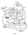
[0026] 図1は、リソグラフィ大量製造プロセスを実施する製造設備の一部として、リソグラフィ装置LAを100で示している。この例では、製造プロセスは、半導体ウェーハなどの基板上での半導体製品(集積回路)の製造に適している。当業者には、このプロセスの変形型で様々なタイプの基板を処理することで、多岐にわたる製品を製造できると分かるであろう。今日、莫大な商業的価値がある半導体製品の製造は、単なる例として使用される。 FIG. 1 shows a lithographic apparatus LA as 100 as part of a manufacturing facility for performing a lithographic mass manufacturing process. In this example, the manufacturing process is suitable for manufacturing a semiconductor product (integrated circuit) on a substrate such as a semiconductor wafer. Those skilled in the art will appreciate that a wide variety of products can be produced by processing various types of substrates in a variation of this process. Today, the manufacture of semiconductor products of enormous commercial value is used only as an example.
[0027] リソグラフィ装置(または、略して「リソツール」100)内において、測定ステーションMEAは102で示され、露光ステーションEXPは104で示されている。制御ユニットLACUは106で示されている。この例では、各基板は、測定ステーションと、適用されるパターンを有する露光ステーションに滞在する。光学リソグラフィ装置では、例えば、調整された放射線および投影システムを使用して、製品パターンをパターニングデバイスMAから基板に転写するために、投影システムが使用される。これは、放射線感応性レジスト材料の層にパターン像を形成することで行われる。 In the lithographic apparatus (or “lithotool” 100 for short), the measurement station MEA is shown at 102 and the exposure station EXP is shown at 104. The control unit LACU is shown at 106. In this example, each substrate stays at a measurement station and an exposure station having a pattern to be applied. In an optical lithographic apparatus, a projection system is used, for example, to transfer a product pattern from the patterning device MA to the substrate using a coordinated radiation and projection system. This is done by forming a pattern image in a layer of radiation-sensitive resist material.
[0028] 本明細書で使用される「投影システム」という用語は、露光放射を使用するのに適した、または液浸液の使用もしくは真空の使用などの他の要素に適した、屈折式、反射式、反射屈折式、磁気式、電磁式、および静電式光学系、またはそれらの任意の組み合わせを含む任意のタイプの投影システムを包含すると広く解釈すべきである。パターニングMAデバイスはマスクまたはレチクルとすることができ、パターンまたはレチクルは、パターニングデバイスによって透過または反射される放射ビームにパターンを付与する。公知の動作モードとして、ステッピングモードおよび走査モードがある。公知のように、投影システムは、基板およびパターニングデバイス用のサポートおよび位置決めシステムと様々な方法で協同して、基板全体にわたる多数のターゲット部分に所望のパターンを付加することができる。プログラマブルパターニングデバイスは、固定パターンを有するレチクルの代わりに使用することができる。放射には、例えば、深紫外線(DUV)または極紫外線(EUV)周波帯の電磁放射があり得る。本開示は、他のタイプのリソグラフィプロセス、例えば、電子ビームによる、例えば、インプリントリソグラフィおよびダイレクトライティングリソグラフィにも適用可能である。 [0028] As used herein, the term "projection system" refers to a refractive, suitable for using exposure radiation or for other factors, such as using an immersion liquid or using a vacuum. It should be broadly interpreted as encompassing any type of projection system, including catadioptric, catadioptric, magnetic, electromagnetic, and electrostatic optics, or any combination thereof. The patterning MA device may be a mask or a reticle, the pattern or reticle imparts a pattern to a radiation beam that is transmitted or reflected by the patterning device. Known operation modes include a stepping mode and a scanning mode. As is known, a projection system can cooperate in various ways with a support and positioning system for a substrate and a patterning device to apply a desired pattern to multiple target portions throughout the substrate. A programmable patterning device can be used instead of a reticle having a fixed pattern. The radiation can include, for example, electromagnetic radiation in the deep ultraviolet (DUV) or extreme ultraviolet (EUV) waveband. The present disclosure is also applicable to other types of lithographic processes, for example, by electron beam, for example, imprint lithography and direct writing lithography.
[0029] リソグラフィ装置制御ユニットLACUは、装置LAに基板WおよびレチクルMAを受け入れさせ、パターン形成処理を実施させるために、様々なアクチュエータおよびセンサの動作および測定を制御する。LACUには、装置の動作に関連する所望の計算を実施する信号処理およびデータ処理能力もある。実際に、制御ユニットLACUは、それぞれがリアルタイムのデータ取得、処理、および装置内のサブシステムまたはコンポーネントの制御を取り扱う多数のサブユニットからなるシステムとして具現化される。 [0029] The lithographic apparatus control unit LACU controls the operation and measurement of various actuators and sensors to cause the apparatus LA to receive the substrate W and the reticle MA and perform a patterning process. The LACU also has signal and data processing capabilities to perform desired calculations related to the operation of the device. In practice, the control unit LACU is embodied as a system consisting of a number of sub-units, each handling real-time data acquisition, processing and control of subsystems or components within the device.
[0030] 基板は、様々な予備ステップが実施できるように、露光ステーションEXPでパターンが基板に付加される前に、測定ステーションMEAで処理される。予備ステップは、高さセンサを使用して、基板の面高さをマッピングすること、およびアライメントセンサを使用して、基板のアライメントマークの位置を測定することを含むことができる。アライメントマークは、通常、規則的な格子パターンに配置される。しかし、マークを形成する際の不正確さにより、さらに、基板の処理全体を通して発生する基板の変形により、マークは理想的な格子から外れる。このため、装置が、製品フィーチャをきわめて高い精度で正確な位置にプリントする場合に、基板の位置および向きを測定することに加えて、実際上、アライメントセンサが、基板領域全体にわたって、多数のマークの位置を詳細に測定しなければならない。装置は、制御ユニットLACUによって制御される位置決めシステムをそれぞれが含む2つの基板テーブルを有する、いわゆる2段タイプとすることができる。一方の基板テーブルに載った1つの基板が、露光ステーションEXPで露光されている間、別の基板は、様々な予備ステップを実施できるように、測定ステーションMEAで他方の基板テーブルに載せることができる。したがって、アライメントマークの測定は非常に時間がかかり、2つの基板テーブルを設けることで、装置のスループットの大幅な向上が可能になる。基板テーブルが測定ステーションおよび露光ステーションにある間、位置センサIFが、基板テーブルの位置を測定できない場合に、両方のステーションで基板テーブルの位置を探知するのを可能にする第2の位置センサを設けることができる。リソグラフィ装置LAは、例えば、2つの基板テーブルWTa、WTbと、基板テーブルを交換することができる2つのステーション(露光ステーションおよび測定ステーション)を有する、いわゆる2段タイプとすることができる。 [0030] The substrate is processed at a measuring station MEA before a pattern is added to the substrate at an exposure station EXP so that various preparatory steps can be performed. Preliminary steps can include mapping the surface height of the substrate using a height sensor and measuring the position of an alignment mark on the substrate using an alignment sensor. The alignment marks are usually arranged in a regular grid pattern. However, due to the inaccuracy in forming the marks and the deformation of the substrate that occurs throughout the processing of the substrate, the marks deviate from the ideal grid. Because of this, in addition to measuring the position and orientation of the substrate when the device prints product features at very precise and precise locations, in practice, the alignment sensor may require a large number of marks over the entire substrate area. Must be measured in detail. The apparatus can be of the so-called two-stage type, with two substrate tables each containing a positioning system controlled by a control unit LACU. While one substrate on one substrate table is being exposed at the exposure station EXP, another substrate can be placed on the other substrate table at the measurement station MEA so that various preliminary steps can be performed. . Therefore, the measurement of the alignment mark takes a very long time, and by providing two substrate tables, it is possible to greatly improve the throughput of the apparatus. While the substrate table is at the measurement station and the exposure station, if the position sensor IF cannot measure the position of the substrate table, a second position sensor is provided which enables both stations to locate the position of the substrate table. be able to. The lithographic apparatus LA can be of a so-called two-stage type, for example, having two substrate tables WTa, WTb and two stations (exposure station and measurement station) where the substrate tables can be exchanged.
[0031] 製造設備内で、装置100は、装置100でパターンを形成するために、感光性レジストおよび他の被覆を基板Wに塗布する被覆装置108も収容する「リソセル」または「リソクラスタ」の一部を形成する。装置100の出力側には、露光されたパターンを現像して物理レジストパターンにするために、焼成装置110および現像装置112が設けられている。これらの全装置間で、基板ハンドリングシステムは、基板の支持と、1つの装置から次の装置への基板の移送とを引き受ける。しばしば一括してトラックと称されるこれらの装置は、トラック制御ユニットの制御下にあり、トラック制御ユニットは、それ自体、監視制御システムSCSによって制御され、監視制御システムSCSはまた、リソグラフィ装置制御ユニットLACUを通してリソグラフィ装置を制御する。こうして、様々な装置は、スループットおよび処理効率を最大限にするように動作することができる。監視制御システムSCSは、各パターン付き基板を形成するために実施されるステップの定義をより詳細に規定したレシピ情報Rを受け取る。 [0031] Within the manufacturing facility, the
[0032] パターンがリソセルにおいて付加され、現像されると、パターン付き基板120は、122、124、126などで示す他の処理装置に移送される。典型的な製造設備の様々な装置によって、様々な処理ステップが実施される。例として、この実施形態の装置122は、エッチングステーションであり、装置124は、エッチング後のアニールステップを行う。さらなる物理的および/または化学的処理ステップがさらなる装置126などに適用される。材料の堆積、表面材料特性の改質(酸化、ドーピング、イオン注入など)、化学機械研磨(CMP)などの様々なタイプの処理が、実際のデバイスを作製するために必要とされ得る。装置126は、実際上、1つまたは複数の装置で実施される一連の様々な処理ステップを表すことができる。 [0032] Once the pattern has been added and developed in the lithocell, the patterned substrate 120 is transferred to another processing device, such as 122, 124, 126, and the like. Various processing steps are performed by various devices of a typical manufacturing facility. By way of example,
[0033] 公知のように、半導体デバイスの製造は、基板の層ごとに適切な材料およびパターンを用いてデバイス構造を構築するために、そのような処理を多数繰り返すことを必要とする。相応して、リソクラスタに到達した基板130は、新たに用意された基板とすることができ、または基板130は、このクラスタで、または全く別の装置ですでに処理された基板とすることができる。同様に、必要とされる処理に応じて、基板132は、装置126から出ると、次のパターン形成処理のために同じリソクラスタに戻すことができ、またはパターン形成処理のために、行き先を異なるクラスタにすることができ、またはダイシングおよびパッケージ化のために送られる完成品とすることができる。 As is known, the manufacture of semiconductor devices requires a number of such processes to be repeated in order to build a device structure using appropriate materials and patterns for each layer of the substrate. Correspondingly, the
[0034] 製品構造の各層は、プロセスステップの異なるセットを必要とし、各層で使用される装置126は、タイプが完全に異なることがある。さらに、装置126によって適用される処理ステップが名目上同じである場合でさえ、大型設備において、様々な基板に対してステップを実施するために、並行して動作するいくつかの同一と考えられる機械があり得る。これらの機械間の構成または欠点の小さな相違は、この小さな相違が、様々な基板に異なる形で影響を及ぼすことを意味し得る。エッチング(装置122)などの比較的各層に共通であるステップでさえ、名目上同一であるが、スループットを最大化するために並行して動作するいくつかのエッチング装置によって実施されることがある。実際上、さらに、様々な層は、エッチングされる材料の細部と、例えば、異方性エッチングなどの特別な要件とに応じて、様々なエッチングプロセス、例えば、化学エッチング、プラズマエッチングを必要とする。 [0034] Each layer of the product structure requires a different set of process steps, and the
[0035] 上記のように、前の、および/または次のプロセスは、他のリソグラフィ装置で実施することができ、様々なタイプのリソグラフィ装置で実施することさえできる。例えば、解像度およびオーバーレイなどのパラメータに関して要求がきわめて厳しい一部の層は、デバイス製造プロセスにおいて、要求があまり厳しくない他の層よりも高度なリソグラフィツールで実施することができる。したがって、一部の層は、液浸タイプのリソグラフィツールで露光することができ、一方、他の層は、「ドライ」ツールで露光される。一部の層は、DUV波長で動作するツールで露光することができ、一方、他の層は、EUV波長の放射線を使用して露光される。 [0035] As noted above, the previous and / or subsequent processes can be performed on other lithographic apparatuses, and can even be performed on various types of lithographic apparatuses. For example, some layers that are very demanding with respect to parameters such as resolution and overlay can be implemented in the device manufacturing process with more sophisticated lithography tools than other less demanding layers. Thus, some layers can be exposed with an immersion type lithography tool, while other layers are exposed with a "dry" tool. Some layers can be exposed with tools that operate at the DUV wavelength, while others are exposed using radiation at the EUV wavelength.
[0036] リソグラフィ装置によって露光される基板が、正確かつ一貫的に露光されるために、露光された基板を検査して、基板層間のオーバーレイエラー、線太さ、クリティカルディメンジョン(CD)などの特性を測定するのが望ましい。相応して、リソセルLCが配置された製造設備は、メトロロジシステムMETも含み、メトロロジシステムMETは、リソセルで処理された基板Wの一部またはすべてを受け入れる。メトロロジの結果は、監視制御システム(SCS)138に直接的に、または間接的に供給される。エラーが検出されると、特に、同じバッチの他の基板がそれでも露光される程度にすぐに、かつ素早くメトロロジを行うことができる場合に、次の基板の露光を調整することができる。また、すでに露光された基板は、歩留まりを改善するために剥がして再処理するか、または廃棄することができ、それにより、欠陥があると分かっている基板に対するさらなる処理の実施を回避する。基板の一部のターゲット部分だけに欠陥がある場合に、良好であるターゲット部分に対してだけ、さらなる露光を実施することができる。 [0036] In order for a substrate exposed by a lithographic apparatus to be accurately and consistently exposed, the exposed substrate is inspected and characteristics such as overlay error, line thickness, and critical dimension (CD) between substrate layers are inspected. It is desirable to measure Correspondingly, the manufacturing facility in which the lithocell LC is located also includes a metrology system MET, which receives some or all of the substrates W processed in the lithocell. The results of the metrology are provided directly or indirectly to a supervisory control system (SCS) 138. If an error is detected, the exposure of the next substrate can be adjusted, especially if the metrology can be performed so quickly and quickly that other substrates of the same batch are still exposed. Also, already exposed substrates can be stripped and reprocessed to improve yield, or discarded, thereby avoiding performing further processing on substrates that are known to be defective. If only some target portions of the substrate are defective, further exposure can be performed only on good target portions.
[0037] 製造プロセスの所望の段階で、製品のパラメータの測定をするために設けられたメトロロジ装置140も図1に示されている。最新のリソグラフィ製造設備のメトロロジ装置の一般的な例には、スキャトロメータ、例えば、角度分解スキャトロメータまたは分光スキャトロメータがあり、このスキャトロメータは、装置122でエッチングを行う前に、120の現像された基板の特性を測定するのに使用することができる。メトロロジ装置140を使用して、例えば、オーバーレイまたはクリティカルディメンジョン(CD)などの重要な性能パラメータが、現像されたレジストにおいて特定の精度要件を満たしていないことを明らかにすることができる。エッチングステップの前に、現像されたレジストを剥がし、リソクラスタによって基板120を再処理する機会が存在する。やはり公知のように、装置140からのメトロロジの結果142を使用して、リソクラスタでのパターン形成処理の高精度な性能を維持し、監視制御システムSCSおよび/または制御ユニットLACU106によって、長期にわたる小調整を行い、それにより、製品が仕様から外れる、および再処理を必要とするリスクを最小限にすることができる。当然のことながら、メトロロジ装置140および/または他のメトロロジ装置(図示せず)は、処理済み基板132、134および投入基板130の特性を測定するのに適用することができる。 [0037] A
例示的な検査装置
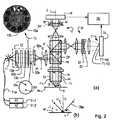
[0038] 図2(a)は、いわゆる暗視野結像メトロロジを実施する検査装置の主要要素を概略的に示している。メトロロジ装置は、スタンドアロン型デバイスとするか、または、例えば、測定ステーションもしくはリソグラフィセルLCのいずれかで、リソグラフィ装置LAに組み込むことができる。装置全体にわたっていくつかの分岐を有する光軸は、点線Oで示されている。ターゲット格子構造Tおよび回折光線は、図2(b)にさらに詳細に示されている。Exemplary inspection device
FIG. 2A schematically shows the main elements of an inspection apparatus that performs so-called dark-field imaging metrology. The metrology apparatus can be a stand-alone device or can be integrated into the lithographic apparatus LA, for example either at the measuring station or at the lithographic cell LC. The optical axis with several branches throughout the device is indicated by the dotted line O. The target grating structure T and the diffracted light beam are shown in more detail in FIG.
[0039] 導入部に記載した先行出願で説明されているように、図2(a)の暗視野結像装置は、分光スキャトロメータの代わりに、または分光スキャトロメータに加えて使用することができる多目的角度分解スキャトロメータの一部とすることができる。このタイプの検査装置では、放射源11から放射された放射線は、照明システム12によって調整される。例えば、照明システム12は、コリメートレンズシステム12a、カラーフィルタ12b、ポラライザ12c、およびアパーチャデバイス13を含むことができる。調整された放射は、照明光路IPをたどり、照明光路IP内で部分反射面15によって反射され、顕微鏡対物レンズ16を介して基板W上のスポットSに合焦される。メトロロジターゲットTは、基板Wに形成することができる。レンズ16は、好ましくは少なくとも0.9、より好ましくは少なくとも0.95の高い開口数(NA)を有する。必要な場合に、液浸流体を使用して1を超える開口数を得ることができる。 As described in the prior application described in the introduction, the dark-field imaging device of FIG. 2A may be used instead of or in addition to a spectroscopic scatterometer. Can be part of a multipurpose angle-resolved scatterometer. In this type of inspection device, the radiation emitted from the radiation source 11 is adjusted by an
[0040] この例での対物レンズ16は、ターゲットによって散乱した放射を収集する働きもする。収集光路CPが、この戻り放射用として概略的に示されている。多目的スキャトロメータは、収集光路に2つ以上の測定分岐を有することができる。瞳結像分岐として図示した例は、瞳結像光学系18および瞳像センサ19を含む。下記にさらに詳細に説明される結像分岐も示されている。さらに、実用装置では、例えば、強度の正規化用、取込みターゲットの粗像形成用、合焦用などの基準放射を収集するためのさらなる光学系および分岐が含まれる。これらの詳細は、上記の先行公報に見ることができる。 [0040] The
[0041] メトロロジターゲットTが基板Wに設けられる場合、メトロロジターゲットTは1D格子とすることができ、1D格子は、現像後に、バーが、連続するレジスト線で形成されるようにプリントされる。ターゲットは2D格子とすることができ、この格子は、現像後に、連続するレジストピラーまたはレジスト内のビアで形成されるようにプリントされる。あるいは、バー、ピラー、またはビアは、基板にエッチングで形成することができる。各これらの格子は、検査装置を使用して特性を調べることができるターゲット構造の例である。格子の場合に、構造は周期的である。 When the metrology target T is provided on the substrate W, the metrology target T can be a 1D grid, which is printed such that after development, the bars are formed by continuous resist lines. You. The target can be a 2D grid, which, after development, is printed such that it is formed by successive resist pillars or vias in the resist. Alternatively, bars, pillars, or vias can be formed in the substrate by etching. Each of these gratings is an example of a target structure that can be characterized using an inspection device. In the case of a lattice, the structure is periodic.
[0042] 照明システム12の様々なコンポーネントは、同じ装置内で様々なメトロロジ「レシピ」を実施するように調整可能である。照明放射の特性として、波長(色)および偏光を選択することに加えて、照明システム12は、様々な照明プロファイルを実施するように調整することができる。アパーチャデバイス13の平面は、対物レンズ16の瞳面および瞳像検出器19の平面と共役である。したがって、アパーチャデバイス13によって決まる照明プロファイルは、基板W上のスポットSへの入射光の角度分布を画定する。様々な照明プロファイルを実施するために、照明光路にアパーチャデバイス13を設けることができる。アパーチャデバイスは、可動式スライダまたはホイールに取り付けられた様々な開口を含むことができる。あるいは、照明光路は、プログラム可能な空間光モジュレータを含むことができる。さらなる代替案として、照明瞳面の様々な位置に光ファイバを配置して、光ファイバのそれぞれの位置に選択的に光を送ったり、または送らなかったりするために使用することができる。これらの変形型は、上記の文献で説明および例示されている。 [0042] The various components of the
[0043] 照明モードに応じて、入射角が図2(b)の「I」で示す通りとなるように例示的な光線30aを供給することができる。ターゲットTによって反射されたゼロ次光線の光路は、「0」と表記されている(光軸「O」と混同しないこと)。同様に、同じ照明モードにおいて、または第2の照明モードにおいて、光線30bを供給することができ、この場合に、入射および反射の角度は、第1のモードと比較して入れ替わる。図2(a)では、第1および第2の例示的な照明モードのゼロ次光線は、それぞれ0a、0bと表記されている。 [0043] Depending on the illumination mode, an
[0044] 図2(b)にさらに詳細に示すように、ターゲット構造の例としてのターゲット格子Tは、基板Wが対物レンズ16の光軸Oに垂直な状態で配置されている。オフアクシス照明プロファイルの場合に、軸Oから外れて角度をなして格子Tに当たった照明Iの光線30aは、ゼロ次光線(実線0)および2つの一次光線(一点鎖線+1および二点鎖線−1)を生じさせる。小ターゲット格子がオーバーフィルされる場合、これらの光線は、メトロロジ格子Tおよび他のフィーチャを含む基板の領域にわたる多数の平行光線の1つにすぎないことを忘れてはならない。照明光線30aのビームは、(有用な光量を収容するのに必要な)有限の幅を有するので、入射光線Iは、事実上、所定の角度範囲を占め、回折光線0および回折光線+1/−1は幾分広がる。小ターゲットの点広がり関数によれば、各次数+1、−1は、示すような単一の理想光線ではなく、所定の角度範囲にわたってさらに広がる。 As shown in more detail in FIG. 2B, the target grating T as an example of the target structure has the substrate W arranged so as to be perpendicular to the optical axis O of the
[0045] 暗視野結像用の収集光路の分岐では、結像光学系20は、基板Wのターゲットの像T’をセンサ23(例えば、CCDまたはCMOSセンサ)に形成する。開口絞り21は、対物レンズ16の瞳面と共役である収集光路CPの結像分岐の平面に設けられている。開口絞り21は、瞳絞りと称されることもある。開口絞り21は、照明開口が様々な形態をとることができるのと同様に、様々な形態をとることができる。開口絞り21は、レンズ16の有効開口と共同して、散乱線のどの部分を使用してセンサ23に像を形成するかを定める。通常、開口絞り21は、ゼロ次回折ビームを遮断するように機能するので、センサ23に形成されるターゲットの像は、一次ビームからのみ形成される。両方の一次ビームが組み合わされて像を形成する例では、この像は、暗視野顕微鏡に相当する、いわゆる暗視野像である。 In the branching of the collection optical path for dark-field imaging, the imaging optical system 20 forms an image T ′ of the target on the substrate W on the sensor 23 (for example, a CCD or CMOS sensor). The
[0046] センサ23によって取り込まれた像は、画像プロセッサおよびコントローラPUに出力され、画像プロセッサおよびコントローラPUの機能は、行われる特定のタイプの測定によって決まる。このために、ターゲット構造の非対称性の測定が行われる。非対称性測定は、ターゲット構造を形成するのに使用されるリソグラフィプロセスの性能パラメータの測定値を求めるために、ターゲット構造の情報と組み合わせることができる。この方法で測定できる性能パラメータには、例えば、オーバーレイ、焦点距離、およびドーズがある。ターゲットの特別な構造は、様々な性能パラメータのこれらの測定が、同じ基本的な非対称性測定法を通じて行われるのを可能にするために設けられる。 [0046] The image captured by
[0047] 再度図2(b)および照明光線30aを参照すると、ターゲット格子からの+1次回折光線は、対物レンズ16に入り、センサ23に像が記録されるのに寄与する。光線30bは、光線30aとは反対の角度で入射し、そのため、−1次回折光線が対物レンズに入り、画像に寄与する。開口絞り21は、オフアクシス照明を使用する場合に、ゼロ次放射線を遮断する。先行公報で説明されているように、照明モードは、XおよびY方向のオフアクシス照明で定義することができる。 Referring again to FIG. 2 (b) and the
[0048] これらの様々な照明モード下で、ターゲット格子の像を比較することで、非対称性の測定値を求めることができる。あるいは、非対称性の測定値は、同じ照明モードを維持するが、ターゲットを回転させることで求めることができる。オフアクシス照明が示されているが、その代わりとして、ターゲットのオンアクシス照明を使用することができ、改良したオフアクシス開口絞り21を使用して、実質的に1つの一次回折光だけをセンサに送ることができる。さらなる例では、オフアクシスプリズム対22が、オンアクシス照明モードと組み合わせて使用される。これらのプリズムは、+1および−1次をセンサ23の様々な位置にそらす効果を有するので、2つの連続する像取込みステップの必要なしに、+1および−1次を検出して比較することができる。例えば、図2(a)では、照明光線30aからの+1次回折を使用して作られる像T’(+1a)は、照明光線30bからの−1次回折を使用して作られる画像T’(−1b)から空間的に分離される。この技術は、上記の公開済みである米国特許出願公開第2011102753A1号に開示されており、この特許の内容は、参照により本明細書に援用される。一次ビームの代わりに、または一次ビームに加えて、二次、三次、さらに高次のビーム(図2に示していない)を測定に使用することができる。さらなるバリエーションとして、オフアクシス照明モードは一定に保つことができ、一方、ターゲット自体は、両側の回折次数を使用して像を取り組むために、対物レンズ16の下で180°回転する。 [0048] Under these various illumination modes, a measurement of asymmetry can be determined by comparing the images of the target grating. Alternatively, a measure of asymmetry can be determined by maintaining the same illumination mode, but rotating the target. Although off-axis illumination is shown, alternatively, on-axis illumination of the target can be used, and using a modified off-
[0049] 従来のレンズに基づく結像システムが説明されたが、本明細書で開示する技術には、プレノプティックカメラ、さらに、いわゆる「レンズレス」または「デジタル」結像システムを同様に適用することができる。したがって、回折放射用の処理システムのどの部分が光領域で実施されるか、およびどれが電子およびソフトウェア領域で実施されるかといった設計上の選択度が高い。 [0049] While a conventional lens-based imaging system has been described, techniques disclosed herein include plenoptic cameras, as well as so-called "lensless" or "digital" imaging systems. Can be applied. Thus, there is a high degree of design choice as to which parts of the processing system for diffracted radiation are implemented in the optical domain and which are implemented in the electronic and software domains.
2波長取込み原理
[0050] 図3は、図2の装置で、2波長の回折スペクトルの同時取込みを可能にする分割式波長選択フィルタの使用法を示している。第1のフィルタ300は、装置の照明光学系のアパーチャデバイス13の代わりに使用される。第1のフィルタ300は、光波長スペクトルの1つまたは複数の第1の通過帯域を有する第1の部分300−1と、1つまたは複数の第2の通過帯域を有する第2の部分300−2とを含む。そのようなフィルタは、異なる特性の2つのフィルタをセグメントに切断し、それらを所望の配置で共に接着することで作製することができる。Two-wavelength acquisition principle
FIG. 3 illustrates the use of a split-type wavelength selective filter that allows simultaneous acquisition of two wavelengths of the diffraction spectrum in the apparatus of FIG. The
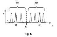
[0051] 分割式フィルタ300の例示的な透過スペクトルが図4に示されている。グラフT−1は、フィルタ300の第1の部分300−1が、波長λに関して低域通過特性を有し、第1の波長範囲402内の波長を有する放射を透過させ、第2の波長範囲404内の波長を有する放射を遮断する。当然のことながら、波長に関する低域通過特性は、周波数またはエネルギに関する広域通過特性に相当する。第2のグラフT−2は、フィルタ300の第2の部分300−1が波長λに関して広域通過特性を有することを示している。これらの部分では、第1の波長範囲402内の波長を有する放射は遮断され、一方、第2の波長範囲404内の放射は透過する。カットオフ波長λCは、2つの波長範囲間の境界を画定している。この例では、カットオフ波長は、2つの部分で等しいように設計されている。通過帯域間に重なりがある場合、これは、重なりの範囲内の波長を有する放射が使用されないという条件で、開示する技術にとって問題ではない。同様に、通過帯域間にギャップがある場合に、これは、単にこのギャップ内の波長を有する放射が使用できないことを意味する。[0051] An exemplary transmission spectrum of the
[0052] 第2のフィルタ310は、開口絞り21の代わりに使用される。フィルタ310は、形態がフィルタ300と非常に類似しており、第1の波長範囲内の放射を透過させ、一方で、第2の波長範囲内の放射を遮断する第1の部分310−1を有し、第2の波長範囲内の放射を透過させ、一方で、第1の波長範囲内の放射を遮断する第2の部分310−1を有する。これらのフィルタ部分のスペクトル透過特性は、図4に示すのと同じである。 [0052] The
[0053] フィルタ300を通る2つの例示的な照明光線302、304が図3に示されている。対応する位置302’、304’が、第2のフィルタ310の図面に示されている。第2のフィルタ310は、その第1の部分310−1が、フィルタの中心を通る光軸Oに関して、瞳面の中の、第1のフィルタ300の第2の部分300−1とは正反対の部分に位置するように配置されていることが分かる。同様に、第2のフィルタ310の第2の部分310−1は、瞳面の中の、第1のフィルタ300の第1の部分300−1とは正反対の部分に位置する。照明光線302、304からのゼロ次反射光線は、第2のフィルタ310の位置302”、304”に到着する。フィルタ300の第1の部分を通る照明光線の角度位置を問わず、対応するゼロ次反射光線は、フィルタ310の第2の部分によって遮断される。同様に、フィルタ300の第2の部分を通る照明光線の角度位置を問わず、対応するゼロ次反射光線は、フィルタ310の第1の部分によって遮断される。 [0053] Two exemplary illumination rays 302, 304 passing through the
[0054] ここでターゲットT(図2(b))によって散乱された一次回折放射を検討すると、302Xは、X方向に周期的な格子構造に当たったときの照明光線302からの回折光線の位置を示している。同様に、302Yは、Y方向に周期的な格子構造に当たったときの照明光線302からの回折光線の位置を示している。さらに、304Xおよび304Yは、照明光線304からの回折光線を示している。各これらの回折光線は、第2のフィルタ310の中の、第1のフィルタ300において照明光線が通過した部分と同じ波長特性を有する部分に入る。したがって、スキャトロメータの収集光学系では、様々な波長の光線は同時に透過することができ、すべての波長および角度位置に対して、より高次の回折光線を通過させ、同時に、ゼロ次の回折光線を遮断する。 Considering now the first order diffracted radiation scattered by the target T (FIG. 2 (b)), 302X is the position of the diffracted light from the
[0055] 収集光学系の光軸に関して、各分割式波長選択フィルタ300、310は、互いに正反対に配置された第1の部分を有するのが分かる。例えば、X方向またはY方向などのターゲット構造の第1の周期方向に交差する第1の対称線320に関して、各分割式波長選択フィルタ300、310は、第2の部分に対称的に対向する第1の部分を有する。同様に、前記構造の第2の周期方向に交差する第2の対称線322に関して、分割式波長選択フィルタは、この場合も、第2の部分に対称的に対向する第1の部分を有する。 [0055] With respect to the optical axis of the collection optical system, it can be seen that each of the split-type wavelength
[0056] 図3に示すフィルタの特定の分割は、上記の米国特許出願公開第2010201963号にさらに詳細に説明されている分割式照明開口に基づく。しかし、単に透過および不透過部分を有するのではなくて、本開示の分割式波長選択フィルタは、相補的にスペクトルを透過させる第1の部分および第2の部分を有する。収集光路CPに第2のそのようなフィルタを適切な向きで配置することで、2つの波長に対する公知の分割式開口の恩恵を同時に受けることができる。所望する場合、分割の他の配置を適用することができる。例えば、一部の用途に対して、2つの半体からなるフィルタを作製するだけで十分であり得る。 [0056] The particular division of the filter shown in FIG. 3 is based on the segmented illumination aperture described in further detail in US Patent Application Publication No. 2010201963, supra. However, rather than simply having transmissive and opaque portions, the segmented wavelength selective filter of the present disclosure has first and second portions that transmit spectra complementarily. Placing a second such filter in the collection path CP in the appropriate orientation can simultaneously benefit from the known split aperture for the two wavelengths. Other arrangements of the split can be applied if desired. For example, for some applications it may be sufficient to make a two-part filter.
[0057] 開口絞りおよび/または瞳絞りの代わりに波長選択フィルタを設けるのではなくて、波長選択フィルタは、従来のアパーチャデバイスおよび/または視野絞りと直列に、別々に取り付けることができる。カラーフィルタ12bは、別の位置をとることができる。 [0057] Rather than providing a wavelength selection filter instead of an aperture stop and / or a pupil stop, the wavelength selection filter can be separately mounted, in series with a conventional aperture device and / or field stop. The
[0058] 再度図2を参照すると、放射源11は、狭帯域放射源対11−1、11−2と、光ファイバ11aなどの共通配送システムとで構築することができる。この例では、第1の放射源11−1は、少なくとも第1の波長範囲内の波長範囲に調節することができ、一方、第2の放射源11−2は、少なくとも第2の波長範囲内の波長範囲に調節することができる。 Referring back to FIG. 2, the radiation source 11 can be constructed with a pair of narrow-band radiation sources 11-1 and 11-2 and a common distribution system such as the optical fiber 11a. In this example, the first radiation source 11-1 can be tuned to at least a wavelength range within the first wavelength range, while the second radiation source 11-2 can be tuned to at least a second wavelength range. Wavelength range.
[0059] 図5は、2つの特定の波長が選択された場合の放射源11の例示的なスペクトル特性を示している。第1の放射源11−1は、第1の波長範囲402内の波長λ1を有する狭帯域放射を供給するように動作している。第2の放射源11−2は、第2の波長範囲404内の波長λ2を有する狭帯域放射を供給するように動作している。フィルタ300、310のセグメントの配置および図4に示すスペクトル特性を再度参照して、両方の波長の回折放射は、同時に検出してメトロロジ目的で使用することができ、一方、両方の波長のゼロ次放射は遮断される。したがって、より一般的には、フィルタ300は、前記収集光学系の瞳面の1つまたは複数の第1の部分にある第1の通過帯域と、瞳面の1つまたは複数の第2の部分にある第2の通過帯域とを有し、第1の部分は、第1の波長の放射を透過させるが、第2の波長の放射を遮断し、第2の部分は、第2の波長の放射を透過さるが、第1の波長の放射を遮断する。 FIG. 5 shows exemplary spectral characteristics of the radiation source 11 when two specific wavelengths are selected. The first radiation source 11-1 is operative to provide narrowband radiation having a wavelength λ1 within the
[0060] 放射の異なる波長は、瞳面で分離されるので、周波数選択フィルタおよび2検出構成の使用に伴い得る透過損失なしに、4分割プリズム22を使用する処理のために分離することができる。原理的には、第1のフィルタ300は、別の適切な方法が、適切な角度分布および波長の照明をもたらすと分かった場合になくすことができる。 [0060] Since the different wavelengths of the radiation are separated at the pupil plane, they can be separated for processing using the
[0061] 図5に示すように、第1の波長λ1は、放射源11−1の制御によって選択できる複数の択一的な第1の波長の1つとすることができる。同様に、第2の波長λ2は、選択できる複数の択一的な第2の波長の1つとすることができる。放射源の構造に応じて、離散波長を選択することができ、または連続調節も可能である。適切な放射源は調節可能なレーザとすることができるが、調節可能なフィルタを備えた広帯域放射源も使用することができる。狭帯域放射の帯域幅は、フィルタ部分の通過帯域内で、所望通りに広く、または狭く選択することができる。 As shown in FIG. 5, the first wavelength λ1 can be one of a plurality of alternative first wavelengths that can be selected by controlling the radiation source 11-1. Similarly, the second wavelength λ2 can be one of a plurality of alternative second wavelengths that can be selected. Depending on the configuration of the radiation source, discrete wavelengths can be selected or continuous tuning is possible. Suitable sources can be tunable lasers, but broadband sources with tunable filters can also be used. The bandwidth of the narrowband radiation can be selected as wide or narrow as desired within the passband of the filter portion.
2波長取込み適用例
[0062] 導入部に記載した既存の小ターゲット回折に基づくオーバーレイ法の原理の説明から始めて、適用例を以下に説明する。2波長取込み原理は、一般に、この特定の適用例に限定されず、暗視野結像メトロロジに限定されない。第2のフィルタ310は、21’において点線で示すように、瞳像センサ19を使用する第1の測定分岐で同様に配置することができる。Two-wavelength acquisition application example
[0062] Starting from the description of the principle of the overlay method based on the existing small target diffraction described in the introduction, an application example will be described below. The two-wavelength acquisition principle is generally not limited to this particular application and is not limited to dark-field imaging metrology. The
[0063] 図6は、公知の手法により基板Wに形成された複合ターゲットを示している。複合ターゲットは、メトロロジ装置の照明ビームによって形成される測定スポットS内にすべてが収まるように、共に接近して配置された格子62〜65の形態の4つの周期構造を含む。円61は、基板W上のスポットSの範囲を示している。4つの格子は、こうしてすべて同時に照明され、センサ23に同時に結像される。それと同時に、上記の本開示の原理によれば、4つの格子は、以下に説明するように、少なくとも第1および第2の波長の放射で同時に照明され、両方の波長の放射で同時に結像される。 FIG. 6 shows a composite target formed on a substrate W by a known method. The composite target includes four periodic structures in the form of gratings 62-65 placed close together so that they all fall within a measurement spot S formed by the illumination beam of the metrology device. A
[0064] 非対称性を測定するのに単一波長のみを使用する場合、オーバーレイメトロロジにおける測定の不確実性の主な原因は、いわゆるプロセス依存である。特に、底部格子の非対称性は、対象となるパラメータであるオーバーレイまたは合焦性能だけでなく、非対称性の測定にも影響を及ぼす。この欠陥を補正する1つの方法は、様々な波長、角度、および/または偏光で多測定することである。実際のオーバーレイは、光の様々な特性の影響を受けにくいが、底部格子の非対称性は様々に反応し、様々な波長で測定したものを組み合わせた非対称性を計算することで補償することができる。不都合なことに、既存の装置では、これらの測定は、波長フィルタを切り換えることで行われ、これは多くの時間がかかる。上記の2波長取込み原理を適用することで、図2の装置は、放射の2つの波長を同時に使用して、非対称性を測定することができる。波長の選択は、検査を受ける製品に存在する多数の層の特定の「スタック」に合わせて調節されるように自由に行うことができる。 When using only a single wavelength to measure asymmetry, a major source of measurement uncertainty in overlay metrology is so-called process dependence. In particular, the asymmetry of the bottom grating affects not only the parameter of interest, overlay or focusing performance, but also the asymmetry measurement. One way to correct for this defect is to make multiple measurements at different wavelengths, angles, and / or polarizations. The actual overlay is less sensitive to various properties of the light, but the asymmetry of the bottom grating responds differently and can be compensated by calculating the combined asymmetry measured at different wavelengths. . Unfortunately, in existing devices, these measurements are made by switching wavelength filters, which is time consuming. By applying the two-wavelength acquisition principle described above, the apparatus of FIG. 2 can measure asymmetry using two wavelengths of radiation simultaneously. The choice of wavelength can be made freely to be tailored to the particular "stack" of multiple layers present in the product under test.
[0065] オーバーレイ測定に専用の例では、格子62〜65は、それ自体、基板Wに形成された半導体デバイスの様々な層にパターン形成された重ね格子で形成された複合格子である。格子62〜65は、複合格子の様々な部分が形成された層間のオーバーレイの測定を容易にするために、様々にずらしたオーバーレイオフセットを有することができる。格子62〜65は、図示したように、XおよびY方向に入射放射を回折させるように格子の向きを違えることもできる。一例では、格子62、64は、それぞれ+d、−dのずれを有するX方向格子である。これは、格子62がそのオーバーレイコンポーネントを有し、これらのコンポーネントは、それらの標準位置に共に正確にプリントされた場合に、コンポーネントの一方が他方に対して距離dだけずれるように配置されることを意味する。格子64は、正確に印刷された場合に、dのオフセットであるが第1の格子などとは反対方向のオフセットがあるように配置されたそのコンポーネントを有する。格子63、65は、それぞれずれ+dおよび−dを有するY方向の格子である。これらの格子の分離像は、センサ23によって取り込まれた像において識別することができる。4つの格子が図示されているが、別の実施形態は、所望の精度を得るために、より大きいマトリクスを必要とすることがある。 [0065] In an example dedicated to overlay measurement, gratings 62-65 are themselves composite gratings formed by superimposed gratings patterned on various layers of semiconductor devices formed on substrate W. Gratings 62-65 may have variously offset overlay offsets to facilitate measurement of the overlay between the layers on which the various portions of the composite grating are formed. Gratings 62-65 can also be oriented differently to diffract incident radiation in the X and Y directions, as shown. In one example,
[0066] 図7は、図2の装置で図6のターゲットを使用し、XおよびYの両方の向きでオフアクシス照明を同時に行う従来の照明プロファイルを使用してセンサ23に形成し、センサ23によって検出することができる像の例を示している。暗色の長方形70は、センサ上の像のフィールドを表し、このフィールド内で、基板上の照明スポット61が、対応する円形領域71に結像されている。この円形領域71内の長方形領域72〜75は、小ターゲット格子62〜65の像を表している。格子が製品領域に配置される場合、製品フィーチャが、このイメージフィールドの周辺に見えることもある。イメージプロセッサおよびコントローラPUは、格子62〜65の分離した像72〜75を識別するために、パターン認識を使用してこれらの像を処理する。この方法では、像は、センサフレーム内の特定の位置にきわめて正確に合わせる必要はなく、これは、測定装置のスループットを全体として大きく向上させる。しかし、結像プロセスが、イメージフィールド全体にわたって不均一になりやすい場合に、依然として、正確に位置合わせする必要がある。本発明の一実施形態では、4つの位置P1〜P4が特定され、格子は、これらの既知の位置に出来るだけ合うようにされる。 FIG. 7 illustrates the use of the target of FIG. 6 in the apparatus of FIG. 2 and the formation of
[0067] 格子の分離像が識別されたのち、これらの個々の像の強度は、例えば、識別された領域内の選択されたピクセル強度値を平均または合計することで評価することができる。像の強度および/または他の特性を互いに比較して、4つ以上の格子の非対称性の測定値を同時に得ることができる。これらの結果をターゲット構造およびバイアススキーム(bias scheme)の情報と組み合わせて、リソグラフィプロセスの様々なパラメータを評価することができる。オーバーレイ性能は、そのようなパラメータの重要な例であり、2つのリソグラフィ層の横方向のアライメントの測度である。オーバーレイは、より具体的には、例えば、底部格子の上部の中心と、対応する上部格子の底部の中心との間の横方向の位置差と定義することができる。リソグラフィプロセスの他のパラメータの測定値を求めるために、様々なターゲット構造を使用することができる。この場合にも、ターゲット構造およびバイアススキームの情報を非対称性の測定値と組み合わせて、所望の性能パラメータの測定値を求めることができる。例えば、このようにして求めた非対称性の測定値からドーズまたは焦点距離の測定値を求める場合に、ターゲット構造は既知である。 [0067] After the separated images of the grid have been identified, the intensity of these individual images can be evaluated, for example, by averaging or summing selected pixel intensity values within the identified region. The intensity and / or other characteristics of the images can be compared to one another to obtain a measure of the asymmetry of four or more gratings simultaneously. These results can be combined with target structure and bias scheme information to evaluate various parameters of the lithographic process. Overlay performance is an important example of such a parameter, a measure of the lateral alignment of the two lithographic layers. An overlay can be more specifically defined, for example, as the lateral position difference between the center of the top of the bottom grid and the center of the bottom of the corresponding top grid. Various target structures can be used to determine measurements of other parameters of the lithographic process. Again, the target structure and bias scheme information can be combined with the asymmetry measurement to determine the desired performance parameter measurement. For example, when a dose or focal length measurement is determined from the asymmetry measurement thus determined, the target structure is known.
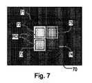
[0068] 従来の装置では、回折の+1および−1次を選択的に使用して、図7に示すタイプの第1および第2の像が得られる。プリズム22を使用することで、回折の+1および−1次の両方を像の分離領域70に取り込むことができる(図示せず)。図8は、説明したばかりの小ターゲットの回折に基づくオーバーレイメトロロジ技術に本開示の2波長取込み原理を適用した場合に、相補的な分割式フィルタ300、310をアパーチャデバイス13および開口絞り21として使用して、暗視野像センサ23上に得ることができる像80を示している。図6の照明スポット61の範囲に相当する単一の領域71の代わりに、ここでは4つの領域81がある。それぞれは、プリズムS22の公知の作用によって、+1または−1回折次数に対応し、それぞれは、分割式波長選択フィルタおよびプリズムS22の作用によって、ここでは別々の波長範囲λ1またはλ2に対応する。各4つの領域内に、複合回折ターゲットの対応する「像」が存在することができ、処理のために分離することができる。長方形領域82には符号が付けられている。垂直方向および斜め方向のハッチングは、図3と同じハッチングによる慣行的手法(hatching convention)を使用して、様々な波長の像を区別するために使用されている。これらの様々な領域の放射は、異なる色(波長)を有し、領域が空間的に分離されることで、単色の像センサ23を使用することが可能になる。 [0068] In conventional devices, the +1 and -1 orders of diffraction are selectively used to obtain first and second images of the type shown in FIG. By using the
[0069] 図9は、分割式波長選択フィルタ300、310の第1の部分および第2の部分が、単純な広域通過または低域通過特性の代わりに、多数の通過帯域を有する代替の実施形態を示している。この実施形態の透過スペクトルT−1、T−2は、2つだけの波長範囲402、404ではなくて、多数の第1の波長範囲902および多数の第2の波長範囲904を有する。これらの透過スペクトルは、「櫛形」フィルタと呼ばれることがある。フィルタの第1の部分の透過スペクトルの各通過帯域は、第2の部分の透過スペクトルの阻止帯域または「ノッチ」に合致する。図4および図5の例と同様に、第1の波長λ1および第2の波長λ2に対して幅広い選択を行うことができる。しかし、図4および図5の例とは対照的に、2つの波長は、図9に示すように、ここでは互いに接近して選択することができる。もはや第1および第2の波長が、関連するスペクトルの異なる半体に含まれる必要はない。適切な特性を有する櫛形フィルタは市販されている。櫛形フィルタは、適切に調整された多層薄膜構造によって、または別々の複数のノッチフィルタを積層することで作製することができる。 FIG. 9 illustrates an alternative embodiment in which the first and second portions of the split-wavelength
[0070] 図10は、上記に概説した装置および方法を使用して、リソグラフィプロセスの性能を評価する方法を示している。ステップS20で、上記の複合格子ターゲットなどのターゲット構造を形成するために、1つまたは複数の基板を処理する。ターゲットの構造は、公知の構造の任意のものまたは新たな構造とすることができる。ターゲットは、装置の第1の測定分岐または第2の測定分岐のどちらを使用するかに応じて、大ターゲットまたは小ターゲット構造とすることができる。ターゲットは、非対称性を通じて、オーバーレイ、焦点距離、またはドーズの測定値を得るために設計することができる。ターゲットは、他の性能パラメータおよび/または非対称性に関係しないパラメータの測定値を得るために設計することができる。線幅またはクリティカルディメンジョンCDは、非対称性の測定を通じてではなく、スキャトロメトリによって測定できるパラメータの例である。CDは、例えば、第1の測定分岐および瞳像センサ19を使用して測定することができる。 FIG. 10 illustrates a method for evaluating the performance of a lithographic process using the apparatus and method outlined above. In step S20, one or more substrates are processed to form a target structure, such as the composite grating target described above. The structure of the target can be any of the known structures or a new structure. The target can be a large target or a small target structure, depending on whether the first measurement branch or the second measurement branch of the device is used. The target can be designed to obtain overlay, focal length, or dose measurements through asymmetry. The target can be designed to obtain measurements of other performance parameters and / or parameters not related to asymmetry. Line width or critical dimension CD is an example of a parameter that can be measured by scatterometry rather than through asymmetry measurements. The CD can be measured, for example, using the first measurement branch and the pupil image sensor 19.
[0071] ステップS21で、単一取込みの2波長を使用した測定のためのレシピを含むメトロロジレシピを定める。波長は上記の通りに選択されて、第1の波長は、フィルタ300、310の第1の部分だけの通過帯域内に含まれ、第2の波長は、フィルタの第2の部分だけの通過帯域内に含まれる。偏光、角度分布などを含むそのようなレシピの通常のパラメータもすべて定められる。 In step S21, a metrology recipe including a recipe for measurement using two wavelengths of single acquisition is determined. The wavelengths are selected as described above, the first wavelength being included in the passband of only the first portion of the
[0072] ステップS22で、図2の検査装置または本開示の原理を実施する他の装置が、2つの波長を同時に使用して、ターゲット構造の1つまたは複数の回折スペクトルを取り込むように動作する。非対称性などの特性は、1つまたは複数のターゲットの取り込んだ回折スペクトルから算出される。両方の波長の回折スペクトルを使用すると、非対称性測定のプロセス依存性が低くなり、オーバーレイ、焦点距離、および/またはドーズなどの性能パラメータのより正確な測定値が得られる。 [0072] In step S22, the inspection apparatus of FIG. 2 or another apparatus implementing the principles of the present disclosure operates to acquire one or more diffraction spectra of the target structure using the two wavelengths simultaneously. . Properties such as asymmetry are calculated from acquired diffraction spectra of one or more targets. The use of diffraction spectra at both wavelengths reduces the process dependence of the asymmetry measurement and provides more accurate measurements of performance parameters such as overlay, focal length, and / or dose.
[0073] ステップS23で、求めた測定値および補助データに応じて、メトロロジレシピを更新することができる。例えば、新たな製品スタック用のメトロロジ技術は開発中のことがある。ステップS24で、図1のリソグラフィ製造設備を動作させる開発および/または製造段階において、リソグラフィプロセス用のレシピが、例えば、その後の基板のオーバーレイを改善するために更新することができる。 [0073] In step S23, the metrology recipe can be updated according to the obtained measured values and auxiliary data. For example, metrology technology for a new product stack may be under development. At step S24, recipes for the lithographic process may be updated, for example, to improve subsequent substrate overlay, during the development and / or manufacturing stages of operating the lithographic manufacturing facility of FIG.
[0074] 測定値を求め、波長の選択および他のレシピパラメータを制御するための計算は、検査装置の像プロセッサおよびコントローラPU内で行うことができる。代替の実施形態では、非対称性および対象となる他のパラメータの計算は、検査装置のハードウェアおよびコントローラPUから遠隔で行うことができる。計算は、例えば、監視制御システムSCS内のプロセッサ、または検査装置のコントローラPUから測定データを受け取るように構成された任意のコンピュータ装置で行うことができる。キャリブレーション測定の制御および処理は、求めた補正値を使用して大量の計算を行うプロセッサとは別のプロセッサで行うことができる。これらのオプションのすべては、実施者(implementer)の選択事項であり、適用される原理または得られる利益を変えるものではない。 [0074] Calculations for determining measurements, controlling wavelength selection and other recipe parameters can be performed in the image processor and the controller PU of the inspection apparatus. In an alternative embodiment, the calculation of the asymmetry and other parameters of interest can be performed remotely from the inspection device hardware and the controller PU. The calculation can be performed, for example, by a processor in the supervisory control system SCS, or any computer device configured to receive measurement data from the controller PU of the inspection device. The control and processing of the calibration measurement can be performed by a processor different from a processor that performs a large amount of calculation using the obtained correction value. All of these options are implementer choices and do not change the principles applied or the benefits obtained.
[0075] 例えば、図3に示すフィルタ300またはフィルタ310は、フィルタの設計対象である波長の固定値を中心とした波長の帯域幅で照明するのに適したフィルタ処理効果をもたらすと本発明人はさらに認識した。要素300または要素310が多数の波長の通過を可能にするならば、それは有益である。メトロロジターゲットを用いた照明ビームの散乱プロセスは回折次数をもたらし、検出システムでの回折次数の位置は、照明ビームの波長と、さらに、メトロロジターゲットの周期とによって決まる。したがって、メトロロジターゲットの周期と、波長または偏光などの照明ビームの状態との特定の組み合わせに対して、多数の回折次数が検出器で重なることが起こり得る。 For example, the present inventor has found that the
[0076] 図11は、フィルタ300またはフィルタ310の実施例を示しており、この実施例は、多波長照明を可能にし、その一方で、回折次数の重なりを回避する。図11のフィルタ300またはフィルタ310は、領域1110、1111、1112を含む。各領域は、波長に対するフィルタとして機能し、所定の波長が通過するのを可能にし、波長は、所定の波長の近辺の帯域幅を有する。例えば、領域1110は、この例では300nm〜500nmのより短い波長を受け入れ、領域1111は、この例では500nm〜600nmの中間波長を受け入れ、領域1112は、この例では600nm〜900nmのより長い波長を受け入れる。 FIG. 11 shows an embodiment of the
[0077] したがって、本発明はさらに、波長選択フィルタを提供し、このフィルタは、第1および第2の部分を含むように分割され、各部分は、多数の波長を透過させるように構成される。 [0077] Accordingly, the present invention further provides a wavelength selective filter, wherein the filter is divided to include first and second portions, each portion configured to transmit multiple wavelengths. .
結論
[0078] 上記に開示した2波長取込み原理は、2つの波長での測定が同時に行われるのを可能にし、スループットを悪化させることなく、測定全体の精度を向上させるのを可能にする。この技術は、暗視野結像法によって行われる非対称性測定の用途に適している。2つの波長を使用することで、非対称性信号のプロセス依存効果が修正されて精度が高まる。小ターゲットを使用することで、照明スポット内の様々な位置での2つ以上の格子の同時読み取り、さらには、2つの波長での回折スペクトルの同時読み取りが可能になる。Conclusion
[0078] The two-wavelength acquisition principle disclosed above allows measurements at two wavelengths to be performed simultaneously and allows for improved overall measurement accuracy without degrading throughput. This technique is suitable for applications of asymmetry measurement performed by dark-field imaging. The use of two wavelengths improves the accuracy by correcting the process dependent effects of the asymmetric signal. The use of a small target allows simultaneous reading of two or more gratings at various locations within the illumination spot, as well as simultaneous reading of diffraction spectra at two wavelengths.
[0079] 本発明の特定の実施形態が上記に説明されたが、当然のことながら、本発明は、説明したものと別の方法で実施することができる。 [0079] While certain embodiments of the invention have been described above, it should be understood that the invention can be practiced otherwise than as described.
[0080] 実施形態で説明した検査装置またはツールは、並列像センサによって、瞳面および基板面を同時結像するための第1および第2の分岐を有するスキャトロメータの特定の形態を含むが、代替の構成も可能である。ビームスプリッタ17を用いて、2つの分岐を対物レンズ16に永続的に接続するのではなくて、分岐は、ミラーなどの可動式光学要素によって選択的に接続することができる。光学系は、単一の像センサを有することができ、瞳面像センサ、さらには基板面像センサとして機能するように、センサへの光路が可動式要素によって再構成される。 The inspection apparatus or tool described in the embodiment includes a specific form of the scatterometer having the first and second branches for simultaneously imaging the pupil plane and the substrate plane by the parallel image sensor. Alternate configurations are possible. Rather than using a beam splitter 17 to permanently connect the two branches to the
[0081] 上記のターゲット構造は、測定を目的として特別に設計および形成されたメトロロジターゲットであるが、他の実施形態では、特性は、基板に形成されたデバイスの機能部分であるターゲットに対して測定することができる。多くのデバイスは、規則的な格子状の構造を有する。本明細書で使用される「ターゲット格子」および「ターゲット構造」という用語は、特に、測定を実施するために構造を設けることを必要としない。 [0081] Although the above target structures are metrology targets specifically designed and formed for measurement purposes, in other embodiments, the characteristics are relative to targets that are functional parts of the device formed on the substrate. Can be measured. Many devices have a regular grid-like structure. The terms "target grating" and "target structure" as used herein do not require, among other things, providing a structure to perform the measurement.
[0082] 実施形態は、検査装置のハードウェアと、基板およびパターニングデバイス上に具現化されるターゲットの適切な周期構造と共に、リソグラフィプロセスについての情報を得るために、上記のタイプの測定方法を実施する、1つまたは複数の一連のマシン可読命令を含むコンピュータプログラムを含むことができる。このコンピュータプログラムは、例えば、図3の装置のコントローラPUおよび/または図2の制御ユニットLACU内で実行することができる。そのようなコンピュータプログラムが格納されたデータ記憶媒体(例えば、半導体メモリ、磁気ディスク、または光ディスク)を設けることもできる。 [0082] Embodiments implement a measurement method of the type described above to obtain information about the lithographic process, together with the inspection apparatus hardware and the appropriate periodic structure of the target embodied on the substrate and the patterning device. Computer program comprising one or more series of machine-readable instructions. This computer program can be executed, for example, in the controller PU of the device of FIG. 3 and / or in the control unit LACU of FIG. A data storage medium storing such a computer program (for example, a semiconductor memory, a magnetic disk, or an optical disk) may be provided.
[0083] 本発明によるさらなる実施形態が、下記の番号を付けた項で説明される。
1.リソグラフィプロセスによって基板に形成された構造の特性を測定する方法であって、
(a1)第1の波長および第1の角度分布を有する第1の放射で構造を照明することと、
(a2)第1の波長とは異なる第2の波長を有し、第2の角度分布を有する第2の放射で構造を照明することと、
(b1)第1の放射が構造によって回折された後、前記第1の放射を収集することと、
(b2)第2の放射が構造によって回折された後、前記第2の放射を収集することと、
(c)構造の前記特性の測定値を導出するために、回折した第1の放射および回折した第2の放射の1つまたは複数の部分を使用することと、
を含み、
照明ステップ(a1)、(a2)は同時に実施され、回折した第1の放射のステップ(c)で使用される部分が、回折した第2の放射のステップ(c)で使用される部分の角度分布と重ならない角度分布を有するように、第1の角度分布と第2の角度分布とを異なるようにし、
収集ステップ(b1)、(b2)は、収集光学系を使用して同時に実施され、収集光学系では、分割式波長選択フィルタが、回折した第1の放射および回折した第2の放射の使用される部分を透過させ、一方、同時に、収集された第1の放射および第2の放射のうちのステップ(c)で使用されない1つまたは複数の他の部分を遮断するように構成される、方法。
2.分割式波長選択フィルタは、前記収集光学系の瞳面の1つまたは複数の第1の部分にある第1の通過帯域と、瞳面の1つまたは複数の第2の部分にある第2の通過帯域とを有し、第1の部分は、第1の波長の放射を透過させるが、第2の波長の放射を遮断し、第2の部分は、第2の波長の放射を透過さるが、第1の波長の放射を遮断する、1項による方法。
3.分割式波長選択フィルタは、前記収集光学系の光軸に関して、互いに直径方向の反対側に配置された第1の部分を有する、2項による方法。
4.分割式波長選択フィルタは、前記構造の第1の周期方向に交差する第1の対称線に関して、第2の部分に対称的に対向する第1の部分を有する、2または3項による方法。
5.分割式波長選択フィルタは、前記構造の第2の周期方向に交差する第2の対称線に関して、第2の部分に対称的に対向する第1の部分を有する、4項による方法。
6.前記第1の波長は、すべてが前記第1の通過帯域内に含まれる利用可能な複数の第1の波長の中から選択される、2〜5項のいずれかによる方法。
7.前記第2の波長は、すべてが前記第2の通過帯域内に含まれる、利用可能な複数の第2の波長の中から選択される、6項による方法。
8.分割式波長選択フィルタは、前記収集光学系の瞳面の1つまたは複数の第1の部分にある複数の第1の通過帯域と、瞳面の1つまたは複数の第2の部分にある複数の第2の通過帯域とを有する、2〜5項による方法。
9.ステップ(a1)、(a2)は、共通の照明光学系を使用して実施され、共通の照明光学系は、第2の分割式波長選択フィルタデバイスを含み、分割式波長選択フィルタは、照明光学系および収集光学系を通るゼロ次光線が、その波長に応じて、前記フィルタの一方、または他方によって遮断されるように向きを合わされる、前出の任意の項による方法。
10.測定される特性は非対称性であり、各ステップ(b1)、(b2)は、
(i)回折放射の第1の選択部分を使用して、構造の第1の像を形成および検出することと、
(ii)構造の回折スペクトルにおいて、第1の部分と対称的に対向する回折放射の第2の選択部分を使用して、構造の第2の像を形成および検出することと、
を含み、
ステップ(c)は、検出した第1および第2の像から導出した強度値に基づいて、構造の非対称性の測定値を計算することを含む、前出の任意の項による方法。
11.ステップ(b1)(i)、ステップ(b2)(i)を同時に実施するために、構造の前記第1の像は、第1の放射および第2の放射を使用して、空間的に分離した位置に形成され、ステップ(b1)(ii)、ステップ(b2)(ii)を同時に実施するために、構造の前記第2の像は、第1の放射および第2の放射の波長を使用して、空間的に分離した位置に形成される、9項による方法。
12.各ステップ(b1)、(b2)、ステップ(i)、(ii)は同時に実施されて、各異なる波長ごとに前記第1の像および第2の像を空間的に分離した位置に形成する、10または11項による方法。
13.複数の周期構造に対する方法によって求めた非対称性に基づいて、前記リソグラフィプロセスの性能パラメータを計算することをさらに含む、10、11、または12項による方法。
14.基板上の構造の特性を測定するように構成された検査装置であって、
−第1の波長および第1の角度分布を有する第1の放射と、第1の波長とは異なる第2の波長を有し、第2の角度分布を有する第2の放射とで構造を同時に照明するように動作可能な照明光学系と、
−第1の放射が構造によって回折された後、前記第1の放射を同時に収集し、第2の放射が構造によって回折された後、前記第2の放射を収集するように動作可能な収集光学系と、
−構造の前記特性の測定値を導出するために、回折した第1の放射および回折した第2の放射の1つまたは複数の部分を使用する処理システムと、
を含み、
回折した第1の放射のうちの前記測定値を導出するために使用される部分が、回折した第2の放射のうちの前記測定値を導出するために使用される部分の角度分布と重ならない角度分布を有するように、第1の角度分布と第2の角度分布とを異なるようにし、
収集光学系は、回折した第1の放射および回折した第2の放射の使用される部分を透過させ、一方、同時に、収集された第1の放射および第2の放射のうちの前記測定値を導出するために使用されない1つまたは複数の他の部分を遮断するように構成された分割式波長選択フィルタを含む、検査装置。
15.分割式波長選択フィルタは、前記収集光学系の瞳面の1つまたは複数の第1の部分にある第1の通過帯域と、瞳面の1つまたは複数の第2の部分にある第2の通過帯域とを有し、第1の部分は、第1の波長の放射を透過させるが、第2の波長の放射を遮断し、第2の部分は、第2の波長の放射を透過さるが、第1の波長の放射を遮断する、14項による検査装置。
16.分割式波長選択フィルタは、前記収集光学系の光軸に関して、互いに直径方向の反対側に配置された第1の部分を有する、15項による検査装置。
17.分割式波長選択フィルタは、前記構造の第1の周期方向に交差する第1の対称線に関して、第2の部分に対称的に対向する第1の部分を有する、15または16項による検査装置。
18.分割式波長選択フィルタは、前記構造の第2の周期方向に交差する第2の対称線に関して、第2の部分に対称的に対向する第1の部分を有する、17項による検査装置。
19.照明光学系は、すべてが前記第1の通過帯域内に含まれる利用可能な複数の第1の波長の中から前記第1の波長を選択するように動作可能である、14〜18項のいずれかによる検査装置。
20.照明光学系は、すべてが前記第2の通過帯域内に含まれる利用可能な複数の第2の波長の中から前記第2の波長を選択するように動作可能である、19項による検査装置。
21.分割式波長選択フィルタは、前記収集光学系の瞳面の1つまたは複数の第1の部分にある複数の第1の通過帯域と、瞳面の1つまたは複数の第2の部分にある複数の第2の通過帯域とを有する、15〜18項による検査装置。
22.照明光学系は、第2の分割式波長選択フィルタを含み、分割式波長選択フィルタは、照明光学系および収集光学系を通るゼロ次光線が、その波長に応じて、前記フィルタの一方、または他方によって遮断されるように向きを合わされる、14〜21項のいずれかによる検査装置。
23.測定される特性は非対称性であり、収集光学系は、構造の回折スペクトルにおいて、(i)回折放射の第1の選択部分を使用して、構造の第1の像を形成および検出し、(ii)第1の部分と対称的に対向する回折放射の第2の選択部分を使用して、構造の第2の像を形成および検出するように、各前記第1の放射および第2の放射に対して動作可能であり、処理システムは、検出した第1および第2の像から導出した強度値に基づいて、構造の非対称性の測定値を計算するように構成される、14〜22項のいずれかによる検査装置。
24.収集光学系は、異なる波長の各第1の放射および第2の放射を同時に使用して、前記第1の像を空間的に分離した位置に形成し、第1の放射および第2の放射を同時に使用して、構造の前記第2の像を空間的に分離した位置に形成するように動作可能である、23項による検査装置。
25.収集光学系は、第1の放射および第2の放射を使用して、構造の前記第1の像を、および第1の放射および第2の放射を使用して、構造の前記第2の像を空間的に分離した位置にすべて同時に形成するように動作可能である、23または24項による検査装置。
26.前記処理システムはさらに、複数の周期構造に対して計算した非対称性に基づいて、前記リソグラフィプロセスの性能パラメータを計算するように構成される、23、24、または25項による検査装置。
27.前記処理システムはさらに、複数の周期構造に対して計算した非対称性に基づいて、前記リソグラフィプロセスの性能パラメータを計算するように構成され、収集光学系は、第1の放射および第2の放射の両方を使用して、複数の構造の様々な波長の前記第1の像と、様々な波長の前記第2の像とを空間的に分離した位置にすべて同時に形成するように動作可能である、26項による検査装置。
28.前記空間的に分離した位置から検出像の前記第1の像および前記第2の像を取り出すことを含む、26または27項による検査装置の処理システムの信号処理部分をプログラム可能な処理デバイスに実行させるマシン可読命令を含むコンピュータプログラム製品。
29.リソグラフィ装置を含むリソグラフィシステムであって、
リソグラフィ装置は、
パターンを照明するように構成された照明光学系と、
パターンの像を基板に投影するように構成された投影光学系と、
26または27項による検査装置と、
を含み、
リソグラフィ装置は、パターンをさらなる基板に付加する際に、検査装置からの測定結果を使用するように構成される、リソグラフィシステム。
30.リソグラフィプロセスを使用して、デバイスパターンが一連の基板に付加される、デバイスを製造する方法であって、1〜13項のいずれかによる方法を使用して、前記デバイスパターンの一部として、または前記デバイスパターンに加えて、前記基板の少なくとも1つに形成された少なくとも1つの構造の特性を測定することと、方法の結果に従って、後の基板に対するリソグラフィプロセスを制御することとを含む方法。
31.光学系で使用する波長選択フィルタであって、少なくとも第1および第2の部分を含むように分割され、1つまたは複数の第1の部分にある少なくとも第1の通過帯域と、1つまたは複数の第2の部分にある少なくとも第2の通過帯域とを有し、第1の部分は、第1の波長の放射を透過させるが、第2の波長の放射を遮断し、第2の部分は、第2の波長の放射を透過させるが、第1の波長の放射を遮断する、波長選択フィルタ。
32.フィルタの光軸に関して、互いに直径方向の反対側に配置された第1の部分を有する、31項によるフィルタ。
33.フィルタの光軸を通る第1の対称線に関して、第2の部分に対称的に対向する第1の部分を有する、31または32項によるフィルタ。
34.前記光軸を通り、第1の対称線に直交する第2の対称線に関して、第2の部分に対称的に対向する第1の部分を有する、33項によるフィルタ。
35.前記第1の部分にある複数の第1の通過帯域と、前記第2の部分にある複数の第2の通過帯域とを有する、31〜34項のいずれかによるフィルタ。
36.それぞれ31〜35項のいずれかに従い、同一の第1の通過帯域および第2の通過帯域を有するフィルタ対。
37.少なくとも2つの波長の放射を使用して照明するための照明光学系と、ターゲット構造と相互作用した後、前記2つの波長を有する放射を収集する収集光学系とを有する検査装置であって、照明光学系および検出光学系の少なくとも1つは、31〜34項のいずれかによる分割式波長選択フィルタを含む、検査装置。
38.各照明光学系および収集光学系は、分割式波長選択フィルタデバイスを含み、2つの光学系の分割式波長選択フィルタは、照明光学系および収集光学系を通るゼロ次光線が、その波長に応じて、前記フィルタの一方、または他方によって遮断されるように向きを合わされる、37項による検査装置。[0083] Further embodiments according to the present invention are described in the numbered sections below.
1. A method for measuring characteristics of a structure formed on a substrate by a lithography process,
(A1) illuminating the structure with a first radiation having a first wavelength and a first angular distribution;
(A2) illuminating the structure with a second radiation having a second wavelength different from the first wavelength and having a second angular distribution;
(B1) collecting the first radiation after the first radiation has been diffracted by the structure;
(B2) collecting the second radiation after the second radiation has been diffracted by the structure;
(C) using one or more portions of the diffracted first radiation and the diffracted second radiation to derive a measurement of the property of the structure;
Including
The illumination steps (a1), (a2) are carried out simultaneously, the part used in step (c) of the diffracted first radiation being the angle of the part used in step (c) of the diffracted second radiation. Making the first angular distribution different from the second angular distribution so as to have an angular distribution that does not overlap with the distribution;
The collecting steps (b1), (b2) are performed simultaneously using collecting optics, in which a split wavelength selective filter uses the diffracted first radiation and the diffracted second radiation. And at least one other portion of the collected first radiation and second radiation not used in step (c) at the same time. .
2. A split-type wavelength selective filter includes a first passband in one or more first portions of a pupil plane of the collection optical system and a second passband in one or more second portions of the pupil plane. A first portion that transmits radiation of the first wavelength, but blocks radiation of the second wavelength, and a second portion that transmits radiation of the second wavelength. , Blocking radiation of the first wavelength.
3. The method according to
4. The method according to
5. 5. The method according to claim 4, wherein the split-type wavelength selective filter has a first portion symmetrically opposite the second portion with respect to a second line of symmetry intersecting the second periodic direction of the structure.
6. The method according to any of
7. 7. The method according to claim 6, wherein said second wavelength is selected from a plurality of available second wavelengths, all of which are comprised within said second passband.
8. The split-type wavelength selection filter includes a plurality of first passbands in one or more first portions of a pupil plane of the collection optical system and a plurality of first passbands in one or more second portions of the pupil plane. The method according to
9. Steps (a1) and (a2) are performed using a common illumination optics, the common illumination optics including a second split wavelength selective filter device, wherein the split wavelength selective filter comprises A method according to any of the preceding clauses, wherein the zero order light passing through the system and the collection optics is directed so as to be blocked by one or the other of said filters, depending on its wavelength.
10. The property measured is asymmetry and each step (b1), (b2) is
(I) forming and detecting a first image of the structure using a first selected portion of the diffracted radiation;
(Ii) forming and detecting a second image of the structure using a second selected portion of the diffracted radiation symmetrically opposite the first portion in a diffraction spectrum of the structure;
Including
A method according to any of the preceding clauses, wherein step (c) comprises calculating a measure of structural asymmetry based on the intensity values derived from the detected first and second images.
11. In order to perform steps (b1) (i), steps (b2) (i) simultaneously, the first image of the structure is spatially separated using a first radiation and a second radiation The second image of the structure uses the wavelengths of the first and second radiations to be formed at a location and to perform steps (b1) (ii), steps (b2) (ii) simultaneously. And forming at spatially separated locations.
12. Steps (b1), (b2), Steps (i) and (ii) are performed simultaneously to form the first image and the second image at spatially separated positions for each different wavelength; Method according to clause 10 or 11.
13. 13. The method according to 10, 11, or 12, further comprising calculating a performance parameter of the lithographic process based on the asymmetry determined by the method for a plurality of periodic structures.
14. An inspection apparatus configured to measure a property of a structure on a substrate,
Simultaneously constructing a structure with a first radiation having a first wavelength and a first angular distribution, and a second radiation having a second wavelength different from the first wavelength and having a second angular distribution; An illumination optical system operable to illuminate,
Collection optics operable to collect the first radiation simultaneously after the first radiation is diffracted by the structure and collect the second radiation after the second radiation is diffracted by the structure; System and
A processing system that uses one or more portions of the diffracted first radiation and the diffracted second radiation to derive a measurement of said property of the structure;
Including
The portion of the diffracted first radiation used to derive the measurement does not overlap the angular distribution of the portion of the diffracted second radiation used to derive the measurement. Making the first angular distribution different from the second angular distribution so as to have an angular distribution,
The collection optics transmit a used portion of the diffracted first radiation and the diffracted second radiation, while simultaneously collecting the measurements of the collected first radiation and second radiation. An inspection apparatus, comprising: a segmented wavelength selective filter configured to block one or more other portions not used for derivation.
15. A split-type wavelength selective filter includes a first passband in one or more first portions of a pupil plane of the collection optical system and a second passband in one or more second portions of the pupil plane. A first portion that transmits radiation of the first wavelength, but blocks radiation of the second wavelength, and a second portion that transmits radiation of the second wavelength. 15. The inspection device according to clause 14, wherein the radiation of the first wavelength is blocked.
16. 16. The inspection apparatus according to
17. 17. The inspection apparatus according to
18. 18. The inspection apparatus according to claim 17, wherein the split-type wavelength selective filter has a first portion symmetrically opposed to the second portion with respect to a second line of symmetry intersecting the second periodic direction of the structure.
19. 19. The illumination optical system of any of clauses 14 to 18, wherein the illumination optics is operable to select the first wavelength from a plurality of available first wavelengths, all of which are included within the first passband. Or inspection equipment.
20. 20. The inspection device according to claim 19, wherein the illumination optics is operable to select the second wavelength from a plurality of available second wavelengths, all of which are included within the second passband.
21. The split-type wavelength selection filter includes a plurality of first passbands in one or more first portions of a pupil plane of the collection optical system and a plurality of first passbands in one or more second portions of the pupil plane. Inspection apparatus according to paragraphs 15-18, having a second passband of
22. The illumination optics includes a second split wavelength selective filter, wherein the zero order light passing through the illumination optics and the collection optics passes one or other of said filters depending on its wavelength. Inspection apparatus according to any of paragraphs 14 to 21, which is oriented so as to be blocked by:
23. The property measured is asymmetric, and the collection optics forms (i) forms and detects a first image of the structure in the diffraction spectrum of the structure using (i) a first selected portion of the diffracted radiation; ii) each said first and second radiation so as to form and detect a second image of the structure using a second selected portion of the diffracted radiation symmetrically opposed to the first portion; 14-22, wherein the processing system is configured to calculate a measure of structural asymmetry based on the intensity values derived from the detected first and second images. Inspection equipment by any of the above.
24. The collection optics uses the first radiation and the second radiation of different wavelengths simultaneously to form the first image at spatially separated locations and to generate the first radiation and the second radiation. 24. An inspection apparatus according to
25. The collection optics uses the first radiation and the second radiation to generate the first image of the structure, and the first radiation and the second radiation to form the second image of the structure. 25. The inspection device according to
26. The inspection apparatus according to
27. The processing system is further configured to calculate a performance parameter of the lithographic process based on the asymmetry calculated for the plurality of periodic structures, wherein the collection optics includes a first radiation and a second radiation. Both are operable to simultaneously form the first images at different wavelengths of the plurality of structures and the second images at different wavelengths in spatially separated locations all at the same time; Inspection apparatus according to paragraph 26.
28. 28. Performing a signal processing portion of a processing system of an inspection apparatus according to 26 or 27 on a programmable processing device, comprising retrieving the first image and the second image of a detected image from the spatially separated locations. A computer program product that includes machine readable instructions for causing
29. A lithography system including a lithographic apparatus, comprising:
Lithographic apparatus
An illumination optics configured to illuminate the pattern;
A projection optical system configured to project an image of the pattern onto the substrate,
An inspection device according to paragraph 26 or 27,
Including
A lithographic system, wherein the lithographic apparatus is configured to use a measurement from the inspection apparatus in applying the pattern to the further substrate.
30. A method of manufacturing a device, wherein a device pattern is applied to a series of substrates using a lithographic process, as part of the device pattern, using a method according to any of
31. A wavelength selection filter for use in an optical system, wherein the wavelength selection filter is divided to include at least a first and a second portion, and includes at least a first passband in one or more first portions and one or more And at least a second passband in a second portion of the first portion, wherein the first portion transmits radiation of the first wavelength but blocks radiation of the second wavelength, and the second portion comprises , A wavelength selective filter that transmits radiation of the second wavelength but blocks radiation of the first wavelength.
32. Clause 31. The filter according to clause 31, having first portions diametrically opposite one another with respect to the optical axis of the filter.
33.
34. 34. The filter according to
35. 33. The filter according to any of claims 31 to 34, having a plurality of first passbands in the first portion and a plurality of second passbands in the second portion.
36. A filter pair having the same first passband and second passband, each according to any of paragraphs 31-35.
37. An inspection apparatus comprising: illumination optics for illuminating using radiation of at least two wavelengths; and collection optics for interacting with a target structure to collect radiation having the two wavelengths, comprising: An inspection apparatus, wherein at least one of the optical system and the detection optical system includes a split-type wavelength selection filter according to any of 31 to 34.
38. Each illumination optics and collection optics includes a split-wavelength selection filter device, and the two optics split-wavelength selection filters allow the zero order light passing through the illumination optics and collection optics to be responsive to its wavelength. Inspection apparatus according to clause 37, oriented so as to be blocked by one or the other of said filters.
[0084] 光リソグラフィとの関連において、本発明の実施形態の使用について上記に特定の言及を行うことができたが、当然のことながら、本発明は、他の用途、例えば、インプリントリソグラフィで使用することができ、状況が可能にする場合、光リソグラフィに限定されない。インプリントリソグラフィでは、パターニングデバイスのトポグラフィが、基板に形成されるパターンを画定する。パターニングデバイスのトポグラフィは、基板に供給されたレジスト層に押し付けることができ、レジストは、電磁放射、熱、圧力、またはそれらの組み合わせを加えることで硬化する。パターニングデバイスは、レジストが硬化した後、レジスト内にパターンを残したままレジストから引き離される。 [0084] Although particular reference has been made above to the use of embodiments of the present invention in the context of optical lithography, it should be understood that the present invention is not limited to other applications, such as imprint lithography. If it can be used and the situation allows, it is not limited to optical lithography. In imprint lithography a topography in a patterning device defines the pattern created on a substrate. The topography of the patterning device can be pressed into a layer of resist supplied to the substrate, and the resist is cured by applying electromagnetic radiation, heat, pressure, or a combination thereof. The patterning device is separated from the resist after the resist has cured, leaving a pattern in the resist.
[0085] 本明細書で使用する「放射」および「ビーム」という用語は、(例えば、365、355、248、193、157、または126nmの波長、あるいはそれらの近辺の波長を有する)紫外(UV)線および(例えば、5〜20nmの範囲の波長を有する)極端紫外(EUV)線、さらには、イオンビームまたは電子ビームなどの粒子ビームを含むすべてのタイプの電磁放射線を包含する。 [0085] As used herein, the terms "radiation" and "beam" refer to ultraviolet (UV) light (e.g., having wavelengths at or near 365, 355, 248, 193, 157, or 126 nm). ) Include all types of electromagnetic radiation, including radiation and extreme ultraviolet (EUV) radiation (e.g., having a wavelength in the range of 5-20 nm), as well as particle beams such as ion beams or electron beams.
[0086] 「レンズ」という用語は、状況が可能にする場合、屈折式、反射式、磁気式、電磁気式、および静電式光学コンポーネントを含む様々なタイプの光学コンポーネントの任意の一つ、またはそれらの組み合わせを指すことができる。 [0086] The term "lens", where the context allows, allows any one of a variety of types of optical components, including refractive, reflective, magnetic, electromagnetic, and electrostatic optical components, or These combinations can be referred to.
[0087] 本発明の広さおよび範囲は、上記の例示的な実施形態のいずれかによって限定されるのではなくて、添付の特許請求の範囲およびその等価物によってのみ規定されるべきである。 [0087] The breadth and scope of the present invention should not be limited by any of the above-described exemplary embodiments, but should be defined only in accordance with the following claims and their equivalents.
Claims (8)
Translated fromJapanese(a1)第1の波長および第1の角度分布を有する第1の放射で前記構造を照明することと、
(a2)前記第1の波長とは異なる第2の波長を有し、第2の角度分布を有する第2の放射で前記構造を照明することと、
(b1)前記第1の放射が前記構造によって回折された後、前記第1の放射を収集することと、
(b2)前記第2の放射が前記構造によって回折された後、前記第2の放射を収集することと、
(c)前記構造の前記特性の測定値を導出するために、前記回折した第1の放射および前記回折した第2の放射の1つまたは複数の部分を使用することと、
を含み、
前記照明ステップ(a1)、(a2)は同時に実施され、ステップ(c)で使用される前記回折した第1の放射の部分が、ステップ(c)で使用される前記回折した第2の放射の部分の角度分布と重ならない角度分布を有するように、前記第1の角度分布と前記第2の角度分布とを異なるようにし、
前記収集ステップ(b1)、(b2)は、収集光学系を使用して同時に実施され、前記収集光学系では、分割式波長選択フィルタが、前記回折した第1の放射および前記回折した第2の放射の使用される部分を透過させるように設けられ、一方、同時に、前記収集された第1の放射および第2の放射のうちのステップ(c)で使用されない1つまたは複数の他の部分を遮断する、方法。A method for measuring characteristics of a structure formed on a substrate by a lithography process,
(A1) illuminating the structure with a first radiation having a first wavelength and a first angular distribution;
(A2) illuminating the structure with a second radiation having a second wavelength different from the first wavelength and having a second angular distribution;
(B1) collecting the first radiation after the first radiation has been diffracted by the structure;
(B2) collecting the second radiation after the second radiation has been diffracted by the structure;
(C) using one or more portions of the diffracted first radiation and the diffracted second radiation to derive a measurement of the property of the structure;
Including
The illuminating steps (a1), (a2) are performed simultaneously and the portion of the diffracted first radiation used in step (c) is replaced by the portion of the diffracted second radiation used in step (c). The first angular distribution and the second angular distribution are different so as to have an angular distribution that does not overlap with the angular distribution of the portion,
The collecting steps (b1) and (b2) are performed simultaneously using collecting optics, in which a split-type wavelength selective filter includes the diffracted first radiation and the diffracted second radiation. Providing one or more other portions of the collected first and second radiation that are not used in step (c), while being provided to transmit a used portion of the radiation. How to cut off.
第1の波長および第1の角度分布を有する第1の放射と、前記第1の波長とは異なる第2の波長を有し、第2の角度分布を有する第2の放射とで構造を同時に照明するように動作可能な照明光学系と、
前記第1の放射が前記構造によって回折された後、前記第1の放射を同時に収集し、前記第2の放射が前記構造によって回折された後、前記第2の放射を収集するように動作可能な収集光学系と、
前記構造の前記特性の測定値を導出するために、前記回折した第1の放射および前記回折した第2の放射の1つまたは複数の部分を使用する処理システムと、
を含み、
前記回折した第1の放射のうちの前記測定値を導出するために使用される部分が、前記回折した第2の放射のうちの前記測定値を導出するために使用される部分の角度分布と重ならない角度分布を有するように、前記第1の角度分布と前記第2の角度分布とを異なるようにし、
前記収集光学系は、前記回折した第1の放射および前記回折した第2の放射の使用される部分を透過させるように設けられ、一方、同時に、前記収集された第1の放射および第2の放射のうちの前記測定値を導出するために使用されない1つまたは複数の他の部分を遮断する分割式波長選択フィルタを含む、検査装置。An inspection device configured to measure a property of a structure on a substrate,
Simultaneously constructing a first radiation having a first wavelength and a first angular distribution and a second radiation having a second wavelength different from said first wavelength and having a second angular distribution. An illumination optical system operable to illuminate,
Operable to collect the first radiation simultaneously after the first radiation is diffracted by the structure and to collect the second radiation after the second radiation is diffracted by the structure. Collection optics,
A processing system that uses one or more portions of the diffracted first radiation and the diffracted second radiation to derive a measurement of the property of the structure;
Including
The portion of the diffracted first radiation used to derive the measurement is the angular distribution of the portion of the diffracted second radiation used to derive the measurement; The first angular distribution and the second angular distribution are different so as to have non-overlapping angular distributions,
The collection optics is arranged to transmit a used portion of the diffracted first radiation and the diffracted second radiation while simultaneously collecting the collected first radiation and a second radiation. An inspection apparatus, comprising: a split wavelength selective filter that blocks one or more other portions of the radiation that are not used to derive the measurement.
前記リソグラフィ装置は、
パターンを照明するように設けられる照明光学系と、
前記パターンの像を基板に投影するように設けられる投影光学系と、
請求項5に記載の検査装置と、
を含み、
前記リソグラフィ装置は、前記パターンをさらなる基板に付加する際に、前記検査装置からの測定結果を使用するように設けられる、リソグラフィシステム。A lithography system including a lithographic apparatus, comprising:
The lithographic apparatus includes:
An illumination optical system provided to illuminate the pattern;
A projection optical system provided to project the image of the pattern onto a substrate,
An inspection device according to claim 5,
Including
A lithographic system, wherein the lithographic apparatus is arranged to use a measurement from the inspection apparatus in applying the pattern to a further substrate.
A method of manufacturing a device, wherein a device pattern is applied to a series of substrates using a lithography process, using the method of claim 1 or 2, as part of the device pattern, or A method comprising, in addition to the device pattern, measuring a property of at least one structure formed on at least one of the substrates, and controlling the lithographic process on a subsequent substrate according to a result of the method. .
Applications Claiming Priority (3)
| Application Number | Priority Date | Filing Date | Title |
|---|---|---|---|
| EP16156466.1 | 2016-02-19 | ||
| EP16156466 | 2016-02-19 | ||
| PCT/EP2017/052594WO2017140528A1 (en) | 2016-02-19 | 2017-02-07 | Method of measuring a structure, inspection apparatus, lithographic system, device manufacturing method and wavelength-selective filter for use therein |
Publications (2)
| Publication Number | Publication Date |
|---|---|
| JP2019509477A JP2019509477A (en) | 2019-04-04 |
| JP6644898B2true JP6644898B2 (en) | 2020-02-12 |
Family
ID=55404630
Family Applications (1)
| Application Number | Title | Priority Date | Filing Date |
|---|---|---|---|
| JP2018540800AActiveJP6644898B2 (en) | 2016-02-19 | 2017-02-07 | Method for measuring structure, inspection apparatus, lithography system, device manufacturing method, and wavelength selective filter used therein |
Country Status (7)
| Country | Link |
|---|---|
| US (2) | US10365565B2 (en) |
| JP (1) | JP6644898B2 (en) |
| KR (1) | KR102106937B1 (en) |
| CN (1) | CN108700824B (en) |
| IL (1) | IL260941B (en) |
| TW (1) | TWI653442B (en) |
| WO (1) | WO2017140528A1 (en) |
Cited By (1)
| Publication number | Priority date | Publication date | Assignee | Title |
|---|---|---|---|---|
| US12072175B2 (en) | 2022-02-28 | 2024-08-27 | Canon Kabushiki Kaisha | Measurement apparatus, measurement method, lithography apparatus and article manufacturing method |
Families Citing this family (16)
| Publication number | Priority date | Publication date | Assignee | Title |
|---|---|---|---|---|
| JP6632252B2 (en)* | 2015-08-21 | 2020-01-22 | キヤノン株式会社 | Detecting device, imprint device, article manufacturing method, and illumination optical system |
| JP6644898B2 (en) | 2016-02-19 | 2020-02-12 | エーエスエムエル ネザーランズ ビー.ブイ. | Method for measuring structure, inspection apparatus, lithography system, device manufacturing method, and wavelength selective filter used therein |
| KR102203005B1 (en)* | 2016-08-30 | 2021-01-14 | 에이에스엠엘 네델란즈 비.브이. | Position sensor, lithographic apparatus and device manufacturing method |
| KR102326190B1 (en)* | 2016-09-12 | 2021-11-15 | 에이에스엠엘 네델란즈 비.브이. | Method and apparatus for inducing correction, method and apparatus for determining properties of structures, method for manufacturing devices |
| US10663866B2 (en)* | 2016-09-20 | 2020-05-26 | Asml Netherlands B.V. | Wavelength-based optical filtering |
| EP3336605A1 (en) | 2016-12-15 | 2018-06-20 | ASML Netherlands B.V. | Method of measuring a structure, inspection apparatus, lithographic system and device manufacturing method |
| JP6818702B2 (en)* | 2018-01-15 | 2021-01-20 | 株式会社東芝 | Optical inspection equipment and optical inspection method |
| EP3528047A1 (en)* | 2018-02-14 | 2019-08-21 | ASML Netherlands B.V. | Method and apparatus for measuring a parameter of interest using image plane detection techniques |
| EP3783438A1 (en)* | 2019-08-21 | 2021-02-24 | ASML Netherlands B.V. | Wavelength selection module, illumination system and metrology system |
| CN112770020A (en) | 2019-11-05 | 2021-05-07 | 北京小米移动软件有限公司 | Image sensing module, method, device, electronic device and medium |
| JP7309640B2 (en)* | 2020-03-18 | 2023-07-18 | 株式会社東芝 | optical inspection equipment |
| JP7468630B2 (en) | 2020-04-13 | 2024-04-16 | 株式会社ニコン | MEASUREMENT APPARATUS, EXPOSURE APPARATUS, AND MEASUREMENT METHOD |
| US11726234B2 (en) | 2020-05-04 | 2023-08-15 | Visera Technologies Company Limited | Optical device |
| JP2023160136A (en)* | 2022-04-21 | 2023-11-02 | キヤノン株式会社 | Calibration method, detection system, exposure device, production method of article, and program |
| US12309510B2 (en)* | 2022-10-07 | 2025-05-20 | Visera Technologies Company Limited | Light-adjusting device and solid-state image sensor using the same |
| WO2025185943A1 (en)* | 2024-03-08 | 2025-09-12 | Asml Netherlands B.V. | Metrology tool and components therefor |
Family Cites Families (40)
| Publication number | Priority date | Publication date | Assignee | Title |
|---|---|---|---|---|
| JPH05204133A (en) | 1992-01-27 | 1993-08-13 | Fujitsu Ltd | Method for inspecting phase shift mask and device for executing this method |
| JPH06241728A (en) | 1993-02-15 | 1994-09-02 | Soltec:Kk | Position shift and gap detection method |
| US5412473A (en) | 1993-07-16 | 1995-05-02 | Therma-Wave, Inc. | Multiple angle spectroscopic analyzer utilizing interferometric and ellipsometric devices |
| WO1996012941A1 (en) | 1994-10-21 | 1996-05-02 | Therma-Wave, Inc. | Spectroscopic ellipsometer |
| US5982489A (en)* | 1996-01-29 | 1999-11-09 | Nikon Corporation | Method and apparatus for measuring depth of a depression in a pattern by light interference from crossed light beams |
| US6469793B1 (en) | 1999-08-10 | 2002-10-22 | Svg Lithography Systems, Inc. | Multi-channel grating interference alignment sensor |
| US6429943B1 (en) | 2000-03-29 | 2002-08-06 | Therma-Wave, Inc. | Critical dimension analysis with simultaneous multiple angle of incidence measurements |
| JP4717363B2 (en) | 2004-03-10 | 2011-07-06 | オリンパス株式会社 | Multispectral imaging device and adapter lens |
| WO2005089417A2 (en)* | 2004-03-17 | 2005-09-29 | Tenebreax Corporation | Color images from monochromatic electro-optical channels |
| US7791727B2 (en) | 2004-08-16 | 2010-09-07 | Asml Netherlands B.V. | Method and apparatus for angular-resolved spectroscopic lithography characterization |
| NL1036245A1 (en) | 2007-12-17 | 2009-06-18 | Asml Netherlands Bv | Diffraction based overlay metrology tool and method or diffraction based overlay metrology. |
| JP2009178200A (en) | 2008-01-29 | 2009-08-13 | Fujifilm Corp | Optical probe and optical tomographic imaging apparatus for OCT |
| NL1036597A1 (en) | 2008-02-29 | 2009-09-01 | Asml Netherlands Bv | Metrology method and apparatus, lithographic apparatus, and device manufacturing method. |
| JP5352111B2 (en) | 2008-04-16 | 2013-11-27 | 株式会社日立ハイテクノロジーズ | Defect inspection method and defect inspection apparatus using the same |
| NL1036857A1 (en) | 2008-04-21 | 2009-10-22 | Asml Netherlands Bv | Inspection method and apparatus, lithographic apparatus, lithographic processing cell and device manufacturing method. |
| CN101299132B (en)* | 2008-05-27 | 2010-06-02 | 上海微电子装备有限公司 | Aligning mark used for photolithography equipment aligning system and its use method |
| NL2004094A (en) | 2009-02-11 | 2010-08-12 | Asml Netherlands Bv | Inspection apparatus, lithographic apparatus, lithographic processing cell and inspection method. |
| KR101461457B1 (en) | 2009-07-31 | 2014-11-13 | 에이에스엠엘 네델란즈 비.브이. | Metrology method and apparatus, lithographic system, and lithographic processing cell |
| CN102483582B (en) | 2009-08-24 | 2016-01-20 | Asml荷兰有限公司 | Metrology method and apparatus, lithography apparatus, lithography processing unit, and substrate including a metrology target |
| JP2011200380A (en)* | 2010-03-25 | 2011-10-13 | Hoya Corp | Light source device for electronic endoscope |
| JP2012026733A (en) | 2010-07-20 | 2012-02-09 | Hitachi High-Technologies Corp | Optical defect detection device and method, and defect observation device provided with the same |
| WO2012022584A1 (en) | 2010-08-18 | 2012-02-23 | Asml Netherlands B.V. | Substrate for use in metrology, metrology method and device manufacturing method |
| CN103201682B (en)* | 2010-11-12 | 2015-06-17 | Asml荷兰有限公司 | Metrology method and apparatus, lithographic system and device manufacturing method |
| WO2012062501A1 (en) | 2010-11-12 | 2012-05-18 | Asml Netherlands B.V. | Metrology method and apparatus, and device manufacturing method |
| JP5747306B2 (en)* | 2011-05-23 | 2015-07-15 | 株式会社ブイ・テクノロジー | Alignment device for exposure equipment |
| NL2008936A (en)* | 2011-07-28 | 2013-01-29 | Asml Netherlands Bv | Illumination source for use in inspection methods and/or lithography inspection and lithographic apparatus and inspection method. |
| WO2013143814A1 (en) | 2012-03-27 | 2013-10-03 | Asml Netherlands B.V. | Metrology method and apparatus, lithographic system and device manufacturing method |
| NL2010458A (en) | 2012-04-16 | 2013-10-17 | Asml Netherlands Bv | Lithographic apparatus, substrate and device manufacturing method background. |
| KR101759608B1 (en) | 2012-05-29 | 2017-07-20 | 에이에스엠엘 네델란즈 비.브이. | Metrology method and apparatus, substrate, lithographic system and device manufacturing method |
| KR101967723B1 (en)* | 2012-07-05 | 2019-04-10 | 에이에스엠엘 네델란즈 비.브이. | Metrology for lithography |
| DE102013204466A1 (en) | 2013-03-14 | 2014-09-18 | Carl Zeiss Smt Gmbh | Measurement of an optical symmetry property on a projection exposure apparatus |
| US10429319B2 (en) | 2013-03-20 | 2019-10-01 | Kla-Tencor Corporation | Inspection system including parallel imaging paths with multiple and selectable spectral bands |
| WO2015000673A1 (en)* | 2013-07-03 | 2015-01-08 | Asml Netherlands B.V. | Inspection apparatus and method, lithographic apparatus, lithographic processing cell and device manufacturing method |
| KR101855243B1 (en) | 2013-08-07 | 2018-05-04 | 에이에스엠엘 네델란즈 비.브이. | Metrology method and apparatus, lithographic system and device manufacturing method |
| TWI530749B (en)* | 2014-06-06 | 2016-04-21 | 台達電子工業股份有限公司 | Illumination module and manufacturing method of color wheel |
| WO2016015734A1 (en) | 2014-08-01 | 2016-02-04 | Dfm A/S | A scatterometer apparatus |
| CN104483817A (en) | 2014-12-25 | 2015-04-01 | 中国科学院长春光学精密机械与物理研究所 | Device for detecting system wave aberration of photoetchingprojection objective |
| CN205608228U (en)* | 2016-01-05 | 2016-09-28 | 深圳市光峰光电技术有限公司 | Light source device |
| JP6644898B2 (en) | 2016-02-19 | 2020-02-12 | エーエスエムエル ネザーランズ ビー.ブイ. | Method for measuring structure, inspection apparatus, lithography system, device manufacturing method, and wavelength selective filter used therein |
| EP3333632A1 (en) | 2016-12-08 | 2018-06-13 | ASML Netherlands B.V. | Metrology apparatus |
- 2017
- 2017-02-07JPJP2018540800Apatent/JP6644898B2/enactiveActive
- 2017-02-07KRKR1020187026217Apatent/KR102106937B1/enactiveActive
- 2017-02-07CNCN201780012412.9Apatent/CN108700824B/enactiveActive
- 2017-02-07WOPCT/EP2017/052594patent/WO2017140528A1/ennot_activeCeased
- 2017-02-17USUS15/435,593patent/US10365565B2/enactiveActive
- 2017-02-18TWTW106105420Apatent/TWI653442B/enactive
- 2018
- 2018-08-01ILIL260941Apatent/IL260941B/enactiveIP Right Grant
- 2019
- 2019-07-29USUS16/524,323patent/US10775704B2/enactiveActive
Cited By (1)
| Publication number | Priority date | Publication date | Assignee | Title |
|---|---|---|---|---|
| US12072175B2 (en) | 2022-02-28 | 2024-08-27 | Canon Kabushiki Kaisha | Measurement apparatus, measurement method, lithography apparatus and article manufacturing method |
Also Published As
| Publication number | Publication date |
|---|---|
| JP2019509477A (en) | 2019-04-04 |
| CN108700824B (en) | 2021-02-02 |
| US10775704B2 (en) | 2020-09-15 |
| CN108700824A (en) | 2018-10-23 |
| TW201740097A (en) | 2017-11-16 |
| KR20180110104A (en) | 2018-10-08 |
| US20170242343A1 (en) | 2017-08-24 |
| US10365565B2 (en) | 2019-07-30 |
| WO2017140528A1 (en) | 2017-08-24 |
| KR102106937B1 (en) | 2020-05-07 |
| US20190346771A1 (en) | 2019-11-14 |
| WO2017140528A9 (en) | 2018-12-20 |
| TWI653442B (en) | 2019-03-11 |
| IL260941B (en) | 2021-05-31 |
Similar Documents
| Publication | Publication Date | Title |
|---|---|---|
| JP6644898B2 (en) | Method for measuring structure, inspection apparatus, lithography system, device manufacturing method, and wavelength selective filter used therein | |
| TWI635272B (en) | Computer program product, method and inspection apparatus for measuring properties of a target structure, and method of manufacturing devices | |
| TWI591448B (en) | Method of measuring asymmetry, inspection apparatus, lithographic system and device manufacturing method | |
| JP5280555B2 (en) | Inspection apparatus and method, lithographic apparatus, lithographic processing cell, and device manufacturing method | |
| JP6703612B2 (en) | Method for measuring structure, inspection apparatus, lithography system, and device manufacturing method | |
| KR102374948B1 (en) | How to determine the performance parameters of a process | |
| JP2020519928A (en) | Structure measuring method, inspection apparatus, lithography system, and device manufacturing method | |
| CN108700834B (en) | Illumination system and metrology system | |
| KR102525481B1 (en) | Method and Apparatus for Measuring a Parameter of Interest Using Image Plane Detection Technology | |
| KR101830850B1 (en) | Inspection apparatus and method, lithographic apparatus, lithographic processing cell and device manufacturing method | |
| CN109643072B (en) | Position sensor, lithographic apparatus and method for manufacturing a device | |
| JP7203725B2 (en) | Method for measuring properties of substrate, inspection apparatus, lithography system, and device manufacturing method | |
| CN111149062A (en) | Measuring method and device | |
| US20180292757A1 (en) | Radiation receiving system | |
| CN113227906A (en) | Position measuring device and associated optical element |
Legal Events
| Date | Code | Title | Description |
|---|---|---|---|
| A621 | Written request for application examination | Free format text:JAPANESE INTERMEDIATE CODE: A621 Effective date:20181002 | |
| A977 | Report on retrieval | Free format text:JAPANESE INTERMEDIATE CODE: A971007 Effective date:20190814 | |
| A131 | Notification of reasons for refusal | Free format text:JAPANESE INTERMEDIATE CODE: A131 Effective date:20190819 | |
| A521 | Request for written amendment filed | Free format text:JAPANESE INTERMEDIATE CODE: A523 Effective date:20191119 | |
| TRDD | Decision of grant or rejection written | ||
| A01 | Written decision to grant a patent or to grant a registration (utility model) | Free format text:JAPANESE INTERMEDIATE CODE: A01 Effective date:20191225 | |
| A61 | First payment of annual fees (during grant procedure) | Free format text:JAPANESE INTERMEDIATE CODE: A61 Effective date:20200108 | |
| R150 | Certificate of patent or registration of utility model | Ref document number:6644898 Country of ref document:JP Free format text:JAPANESE INTERMEDIATE CODE: R150 | |
| R250 | Receipt of annual fees | Free format text:JAPANESE INTERMEDIATE CODE: R250 | |
| R250 | Receipt of annual fees | Free format text:JAPANESE INTERMEDIATE CODE: R250 | |
| R250 | Receipt of annual fees | Free format text:JAPANESE INTERMEDIATE CODE: R250 |