JP6643250B2 - Imaging device, imaging method, and program - Google Patents
Imaging device, imaging method, and programDownload PDFInfo
- Publication number
- JP6643250B2 JP6643250B2JP2016564799AJP2016564799AJP6643250B2JP 6643250 B2JP6643250 B2JP 6643250B2JP 2016564799 AJP2016564799 AJP 2016564799AJP 2016564799 AJP2016564799 AJP 2016564799AJP 6643250 B2JP6643250 B2JP 6643250B2
- Authority
- JP
- Japan
- Prior art keywords
- captured image
- unit
- white balance
- bayerization
- level
- Prior art date
- Legal status (The legal status is an assumption and is not a legal conclusion. Google has not performed a legal analysis and makes no representation as to the accuracy of the status listed.)
- Expired - Fee Related
Links
Images


Classifications
- G—PHYSICS
- G06—COMPUTING OR CALCULATING; COUNTING
- G06T—IMAGE DATA PROCESSING OR GENERATION, IN GENERAL
- G06T3/00—Geometric image transformations in the plane of the image
- G06T3/40—Scaling of whole images or parts thereof, e.g. expanding or contracting
- G06T3/4015—Image demosaicing, e.g. colour filter arrays [CFA] or Bayer patterns
- H—ELECTRICITY
- H04—ELECTRIC COMMUNICATION TECHNIQUE
- H04N—PICTORIAL COMMUNICATION, e.g. TELEVISION
- H04N23/00—Cameras or camera modules comprising electronic image sensors; Control thereof
- H04N23/70—Circuitry for compensating brightness variation in the scene
- H04N23/71—Circuitry for evaluating the brightness variation
- H—ELECTRICITY
- H04—ELECTRIC COMMUNICATION TECHNIQUE
- H04N—PICTORIAL COMMUNICATION, e.g. TELEVISION
- H04N23/00—Cameras or camera modules comprising electronic image sensors; Control thereof
- H04N23/80—Camera processing pipelines; Components thereof
- H04N23/84—Camera processing pipelines; Components thereof for processing colour signals
- H04N23/88—Camera processing pipelines; Components thereof for processing colour signals for colour balance, e.g. white-balance circuits or colour temperature control
- H—ELECTRICITY
- H04—ELECTRIC COMMUNICATION TECHNIQUE
- H04N—PICTORIAL COMMUNICATION, e.g. TELEVISION
- H04N25/00—Circuitry of solid-state image sensors [SSIS]; Control thereof
- H04N25/10—Circuitry of solid-state image sensors [SSIS]; Control thereof for transforming different wavelengths into image signals
- H04N25/11—Arrangement of colour filter arrays [CFA]; Filter mosaics
- H04N25/13—Arrangement of colour filter arrays [CFA]; Filter mosaics characterised by the spectral characteristics of the filter elements
- H04N25/131—Arrangement of colour filter arrays [CFA]; Filter mosaics characterised by the spectral characteristics of the filter elements including elements passing infrared wavelengths
- H—ELECTRICITY
- H04—ELECTRIC COMMUNICATION TECHNIQUE
- H04N—PICTORIAL COMMUNICATION, e.g. TELEVISION
- H04N25/00—Circuitry of solid-state image sensors [SSIS]; Control thereof
- H04N25/10—Circuitry of solid-state image sensors [SSIS]; Control thereof for transforming different wavelengths into image signals
- H04N25/11—Arrangement of colour filter arrays [CFA]; Filter mosaics
- H04N25/13—Arrangement of colour filter arrays [CFA]; Filter mosaics characterised by the spectral characteristics of the filter elements
- H04N25/133—Arrangement of colour filter arrays [CFA]; Filter mosaics characterised by the spectral characteristics of the filter elements including elements passing panchromatic light, e.g. filters passing white light
- H—ELECTRICITY
- H04—ELECTRIC COMMUNICATION TECHNIQUE
- H04N—PICTORIAL COMMUNICATION, e.g. TELEVISION
- H04N25/00—Circuitry of solid-state image sensors [SSIS]; Control thereof
- H04N25/10—Circuitry of solid-state image sensors [SSIS]; Control thereof for transforming different wavelengths into image signals
- H04N25/11—Arrangement of colour filter arrays [CFA]; Filter mosaics
- H04N25/13—Arrangement of colour filter arrays [CFA]; Filter mosaics characterised by the spectral characteristics of the filter elements
- H04N25/135—Arrangement of colour filter arrays [CFA]; Filter mosaics characterised by the spectral characteristics of the filter elements based on four or more different wavelength filter elements
- H—ELECTRICITY
- H04—ELECTRIC COMMUNICATION TECHNIQUE
- H04N—PICTORIAL COMMUNICATION, e.g. TELEVISION
- H04N2209/00—Details of colour television systems
- H04N2209/04—Picture signal generators
- H04N2209/041—Picture signal generators using solid-state devices
- H04N2209/042—Picture signal generators using solid-state devices having a single pick-up sensor
- H04N2209/045—Picture signal generators using solid-state devices having a single pick-up sensor using mosaic colour filter
- H—ELECTRICITY
- H04—ELECTRIC COMMUNICATION TECHNIQUE
- H04N—PICTORIAL COMMUNICATION, e.g. TELEVISION
- H04N23/00—Cameras or camera modules comprising electronic image sensors; Control thereof
- H04N23/10—Cameras or camera modules comprising electronic image sensors; Control thereof for generating image signals from different wavelengths
- H04N23/11—Cameras or camera modules comprising electronic image sensors; Control thereof for generating image signals from different wavelengths for generating image signals from visible and infrared light wavelengths
Landscapes
- Engineering & Computer Science (AREA)
- Multimedia (AREA)
- Signal Processing (AREA)
- Physics & Mathematics (AREA)
- Spectroscopy & Molecular Physics (AREA)
- General Physics & Mathematics (AREA)
- Theoretical Computer Science (AREA)
- Color Television Image Signal Generators (AREA)
- Processing Of Color Television Signals (AREA)
Description
Translated fromJapanese本開示は、撮像装置、撮像方法、およびプログラムに関し、特に、ベイヤ配列の撮像画像の露光制御方法で、非ベイヤ配列の撮像画像の露光制御を行うことができるようにした撮像装置、撮像方法、およびプログラムに関する。 The present disclosure relates to an image capturing apparatus, an image capturing method, and a program, and in particular, an image capturing apparatus, an image capturing method, and an image capturing method that can perform exposure control of a captured image in a non-Bayer array using an exposure control method for a captured image in a Bayer array. And about the program.
RGBW画素配列のイメージセンサにおいて、不可視光である近赤外光と可視光の両方を透過させる光学帯域分離フィルタを介して入力された光に対応する画像を撮像し、撮像画像から不可視光成分と可視光成分を分離することが考案されている(例えば、特許文献1参照)。このようなイメージセンサにおいて、不可視光成分と可視光成分の分離を高精度で行うためには、適切な露光制御を行うことが必要である。 In an image sensor with an RGBW pixel array, an image corresponding to light input through an optical band separation filter that transmits both near-infrared light and visible light that are invisible light is captured, and an invisible light component is extracted from the captured image. It has been devised to separate visible light components (for example, see Patent Document 1). In such an image sensor, it is necessary to perform appropriate exposure control in order to separate the invisible light component and the visible light component with high accuracy.
そこで、分離の前後に積分器を設け、不可視光成分の量に応じて一方からの出力を選択して用いることにより、露光制御(AE(Automatic Exposure)制御)やホワイトバランス制御(AWB(Automatic White-Balance)制御)を行うことが考えられている(例えば、特許文献2参照)。 Therefore, an integrator is provided before and after separation, and an output from one of them is selected and used according to the amount of the invisible light component, so that exposure control (AE (Automatic Exposure) control) and white balance control (AWB (Automatic White -Balance) control (for example, see Patent Document 2).
しかしながら、特許文献2に記載の露光制御方法のように、ベイヤ配列の撮像画像の露光制御方法とは大きく異なる方法を用いて露光制御を行う場合、既存のベイヤ配列の撮像画像の露光制御部では、露光制御を行うことができない。従って、新たな露光制御部を開発し、設置する必要があり、製造コストが増加する。 However, when performing exposure control using a method that is significantly different from the exposure control method of the Bayer array captured image as in the exposure control method described in
よって、ベイヤ配列の撮像画像の露光制御方法で、不可視光成分と可視光成分を含むRGBW画素配列の撮像画像などの非ベイヤ配列の撮像画像の露光制御を行うことが望まれている。 Therefore, it is desired to control the exposure of a non-Bayer array captured image, such as an RGBW pixel array captured image including an invisible light component and a visible light component, using a Bayer array captured image exposure control method.
本開示は、このような状況に鑑みてなされたものであり、ベイヤ配列の撮像画像の露光制御方法で、非ベイヤ配列の撮像画像の露光制御を行うことができるようにするものである。 The present disclosure has been made in view of such a situation, and it is an object of the present disclosure to perform exposure control of a captured image in a non-Bayer array using an exposure control method for a captured image in a Bayer array.
本開示の一側面の撮像装置は、非ベイヤ配列の撮像画像に対してベイヤ化処理を行う際、ベイヤ化処理前の前記撮像画像の最も感度の高い画素の信号レベルである前レベルと、ベイヤ化処理後の前記撮像画像の、ベイヤ配列の画像の露光制御に用いられる画素の信号レベルである後レベルが同一になるように、前記撮像画像の信号レベルを補正するレベル補正部を備える撮像装置である。 An imaging apparatus according to an embodiment of the present disclosure, when performing a Bayerization process on a captured image in a non-Bayer array, includes a previous level that is a signal level of a pixel with the highest sensitivity of the captured image before the Bayerization process, Imaging apparatus comprising a level correction unit that corrects the signal level of the captured image so that the post-level, which is the signal level of the pixel used for exposure control of the image of the Bayer array, of the captured image after the conversion processing is the same It is.
本開示の一側面の撮像方法およびプログラムは、本開示の一側面の撮像装置に対応する。 An imaging method and a program according to an embodiment of the present disclosure correspond to an imaging device according to an embodiment of the present disclosure.
本開示の一側面においては、非ベイヤ配列の撮像画像に対してベイヤ化処理を行う際、ベイヤ化処理前の前記撮像画像の最も感度の高い画素の信号レベルである前レベルと、ベイヤ化処理後の前記撮像画像の、ベイヤ配列の画像の露光制御に用いられる画素の信号レベルである後レベルが同一になるように、前記撮像画像の信号レベルが補正される。 According to an embodiment of the present disclosure, when performing a Bayerization process on a captured image in a non-Bayer array, a previous level that is a signal level of a pixel with the highest sensitivity of the captured image before the Bayerization process, and a Bayerization process The signal level of the captured image is corrected so that the subsequent level, which is the signal level of the pixel used for exposure control of the Bayer array image, of the subsequent captured image is the same.
本開示の一側面によれば、撮像することができる。また、本開示の一側面によれば、ベイヤ配列の撮像画像の露光制御方法で、非ベイヤ配列の撮像画像の露光制御を行うことができる。 According to an embodiment of the present disclosure, imaging can be performed. Further, according to an embodiment of the present disclosure, it is possible to perform exposure control of a captured image having a non-Bayer array using the exposure control method of a captured image having a Bayer array.
なお、ここに記載された効果は必ずしも限定されるものではなく、本開示中に記載されたいずれかの効果であってもよい。 Note that the effects described here are not necessarily limited, and may be any of the effects described in the present disclosure.
以下、本開示を実施するための形態(以下、実施の形態という)について説明する。なお、説明は以下の順序で行う。
1.第1実施の形態:撮像システム(図1乃至図13)
2.第2実施の形態:撮像システム(図14乃至図17)
3.非ベイヤ配列の他の例(図18)
4.第3実施の形態:コンピュータ(図19)Hereinafter, embodiments for implementing the present disclosure (hereinafter, referred to as embodiments) will be described. The description will be made in the following order.
1. First Embodiment: an imaging system (FIGS. 1 to 13)
2. Second embodiment: imaging system (FIGS. 14 to 17)
3. Another example of non-Bayer arrangement (FIG. 18)
4. Third Embodiment: Computer (FIG. 19)
<第1実施の形態>
(撮像装置の第1実施の形態の構成例)
図1は、本開示を適用した撮像装置を含む撮像システムの第1実施の形態の構成例を示すブロック図である。<First embodiment>
(Configuration Example of First Embodiment of Imaging Apparatus)
FIG. 1 is a block diagram illustrating a configuration example of a first embodiment of an imaging system including an imaging device to which the present disclosure is applied.
図1の撮像システム10は、撮像装置11とIR(赤外光)投光装置12により構成される。撮像システム10では、被写体によって反射された赤外光と可視光に対応する画像が撮像される。 The
具体的には、撮像装置11は、レンズ21、光学フィルタ22、イメージセンサ23、ベイヤ化処理部24、および信号処理部25により構成される。 Specifically, the
撮像装置11のレンズ21には、被写体からの光が入射される。レンズ21は、入射された光を、光学フィルタ22を介してイメージセンサ23に集光させる。光学フィルタ22は、入射された光のうちの赤外光と可視光を透過させる。なお、光学フィルタ22は設けられなくてもよい。 Light from a subject enters the
イメージセンサ23は、CMOS(Complementary Metal-Oxide Semiconductor)イメージセンサまたはCCD(Charge Coupled Device)イメージセンサであり、RGBW画素配列の画素を有する。イメージセンサ23は、画素ごとに、入射された赤外光と、可視光のうちの、その画素に対応する色(赤色(R)、緑色(G)、青色(B)、白色(W))の光とを受光し、受光量に応じた電気信号を画素信号として生成することにより、撮像を行う。従って、撮像の結果得られる各画素の画素信号には、不可視光成分としての赤外光成分と可視光成分とが含まれる。イメージセンサ23は、撮像の結果得られる各画素の画素信号を、撮像画像としてベイヤ化処理部24に供給する。 The
ベイヤ化処理部24は、イメージセンサ23から供給される非ベイヤ配列の撮像画像に対してベイヤ化処理(リモザイク処理)を行い、ベイヤ配列(RGB画素配列)のRGB画像を生成する。ベイヤ化処理部24は、生成されたベイヤ配列のRGB画像を信号処理部25に供給する。 The Bayer
信号処理部25は、既存のベイヤ配列の撮像画像用の信号処理部である。信号処理部25は、ベイヤ化処理部24から供給されるRGB画像を用いて、ベイヤ配列の撮像画像に対する方法と同一の方法で、露光制御処理、ホワイトバランス制御処理、YCbCr変換処理などの信号処理を行う。信号処理部25は、露光制御処理の結果得られる露光量を表すシャッタゲインをイメージセンサ23に供給し、撮像画像の露光量を制御する。また、信号処理部25は、RGB画像に対してホワイトバランス制御処理およびYCbCr変換処理を行った結果得られるYCbCr画像を出力する。 The
IR投光装置12は、例えば、可視光が少ない夜間に、被写体に向けて赤外光を出射する。 The
(光学フィルタの各波長の光の透過率の例)
図2は、図1の光学フィルタ22の各波長の光の透過率の例を示す図である。(Example of transmittance of light of each wavelength of optical filter)
FIG. 2 is a diagram illustrating an example of the transmittance of the
図2のグラフにおいて、横軸は、光学フィルタ22を通過する光の波長(nm)を表し、縦軸は、その光の透過率(%)を表す。 In the graph of FIG. 2, the horizontal axis represents the wavelength (nm) of light passing through the
図2に示すように、光学フィルタ22では、波長が約390nm〜660nmである可視光の透過率と、波長が約820nm〜910nmである赤外光の透過率が0%より大きい。従って、光学フィルタ22では、波長が約390nm〜660nmである可視光と波長が約820nm〜910nmである赤外光が通過する。 As shown in FIG. 2, in the
(ベイヤ化処理の前後の画像の画素配列の説明)
図3は、図1のベイヤ化処理部24によるベイヤ化処理の前後の画像の画素配列を説明する図である。(Explanation of pixel array of image before and after Bayerization processing)
FIG. 3 is a diagram illustrating a pixel arrangement of an image before and after Bayerization processing by the
図3のAに示すように、ベイヤ化処理前の画像、即ちイメージセンサ23から出力される撮像画像の画素配列は、RGBW画素配列である。また、各画素の画素信号には赤外光(IR)成分が含まれる。 As shown in FIG. 3A, the pixel array of the image before Bayerization processing, that is, the captured image output from the
ベイヤ化処理部24は、このようなベイヤ化処理前の画像に対して、ベイヤ化処理を行うことにより、図3のBに示すRGB画素配列の画像を、ベイヤ化処理後の画像として生成する。 The
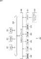
(ベイヤ化処理部の構成例)
図4は、図1のベイヤ化処理部24の構成例を示すブロック図である。(Configuration example of Bayerization processing unit)
FIG. 4 is a block diagram illustrating a configuration example of the
ベイヤ化処理部24は、低周波処理部41、分離部42、ゲイン算出部43、ホワイトバランス部44、レベル補正部45、YC変換部46、輝度合成部47、飽和色消し部48、クロマゲインアンプ49、RGB変換部50、高周波補完部51、高周波抽出部52、高周波復元処理部53、逆ホワイトバランス部54、およびベイヤ化部55から構成される。ベイヤ化処理部24は、図1のイメージセンサ23から供給される撮像画像を高周波成分と低周波成分に分離して、ベイヤ化処理を行う。 The
具体的には、ベイヤ化処理部24の低周波処理部41は、イメージセンサ23の画素の色ごとに、イメージセンサ23から供給される撮像画像に対してLPF(Low Pass Filter)処理および補完処理を行う。低周波処理部41は、その結果生成される赤外光成分を含む全画素の各色の同時刻の画素信号の低周波成分(W+IR)L,(R+IR)L,(G+IR)L、および(B+IR)Lを分離部42に供給し、低周波成分(W+IR)Lをゲイン算出部43、輝度合成部47、高周波抽出部52、および高周波復元処理部53に供給する。Specifically, the low-
分離部42は、低周波処理部41から供給される低周波成分(W+IR)L,(R+IR)L,(G+IR)L、および(B+IR)Lに基づいて、低周波成分(R+IR)L,(G+IR)L,(B+IR)Lのそれぞれに含まれる赤外光成分と可視光成分を、以下の式(1)により分離する。The

なお、IRLは、低周波成分(R+IR)L,(G+IR)L,(B+IR)Lのそれぞれに含まれる赤外光成分である。また、RL,GL,BLは、低周波成分(R+IR)L,(G+IR)L,(B+IR)Lの可視光成分である。Incidentally, IRL represents the low-frequency component(R + IR) L, ( G + IR) L, an infrared light component contained in each of the (B+ IR)L.RL ,GL , andBL are visible light components of low frequency components (R+ IR )L , (G+ IR )L , and (B+ IR )L.
分離部42は、分離の結果得られる赤外光成分IRLと可視光成分RL,GL、およびBLとをゲイン算出部43に供給し、可視光成分RL,GL、およびBLをホワイトバランス部44に供給する。
ゲイン算出部43(ホワイトバランスゲイン算出部)は、分離部42から供給される可視光成分RL,GL、およびBLに基づいて、以下の式(2)により、可視光成分RL,GL、およびBLのホワイトバランスゲインCWR,CWG,CWBを算出し、ホワイトバランス部44に供給する。Gain calculation unit 43 (white balance gain calculation section), the visible light component RL supplied from
なお、AveRL,AveGL,AveBLは、それぞれ、1画面内の可視光成分RL,GL,BLの平均値である。また、ゲイン算出部43は、ホワイトバランスゲインCWR,CWG,CWBの逆数を算出し、逆ホワイトバランス部54に供給する。Incidentally, AveR L, AveG L, AveB L , respectively, the visible light component RL in one screen, the average value of GL, BL. Further, the
さらに、ゲイン算出部43(補正ゲイン算出部)は、ベイヤ配列の撮像画像の露光制御に用いられる画素である緑色の画素の可視光成分(の信号レベル)GL(後レベル)と、低周波処理部41から供給される、撮像画像のうちの最も感度の高い白色の画素の低周波成分(の信号レベル)(W+IR)L(前レベル)とに基づいて、以下の式(3)により、補正ゲインCEを算出する。Further, the gain calculator 43 (correction gain calculator) includes a visible light component (signal level)GL (post-level) of a green pixel, which is a pixel used for exposure control of a captured image in the Bayer array, and a low-frequency component. Based on the low-frequency component (signal level) (W+ IR )L (previous level) of the white pixel with the highest sensitivity in the captured image supplied from the
なお、Ave(W+IR)Lは、1画面内の低周波成分(W+IR)Lの平均値である。式(3)によれば、可視光成分GL(の平均値)を低周波成分(W+IR)L(の平均値)にするための補正ゲインCEが算出される。従って、可視光成分GLと補正ゲインCEを乗算することにより、乗算後の可視光成分GLは、低周波成分(W+IR)Lと同一になる。ゲイン算出部43は、補正ゲインCEをレベル補正部45に供給する。Ave (W+ IR )L is an average value of low frequency components (W+ IR )L in one screen. According to the equation (3), the correction gainCE forconverting the (average value of) the visible light component GL (the average value of the low frequency component (W+ IR )L ) is calculated. Therefore, by multiplying the visible light componentGL by the correction gainCE , the visible light componentGL after the multiplication becomes the same as the low frequency component (W+ IR )L. The
ホワイトバランス部44は、以下の式(4)に示すように、分離部42から供給される可視光成分RL,GL、およびBLのそれぞれに対して、ゲイン算出部43から供給されるホワイトバランスゲインCWR,CWG,CWBを乗算する。これにより、可視光成分RL,GL、およびBLの比率(ホワイトバランス)が補正される。The white balance unit 44 is supplied from the
なお、RWL,GWL、およびBWLは、それぞれ、補正後の可視光成分RL,GL、およびBLである。ホワイトバランス部44は、補正後の可視光成分RWL,GWL、およびBWLをレベル補正部45に供給する。Note that RWL , GWL , and BWL are the corrected visible light components RL , GL , and BL , respectively. The white balance unit 44 supplies the corrected visible light components RWL , GWL , and BWL to the
レベル補正部45は、ベイヤ化処理後のRGB画像の緑色の画素の画素信号と低周波成分(W+IR)Lが同一になるように、ゲイン算出部43からの補正ゲインCEと、ホワイトバランス部44からの可視光成分RWL,GWL、およびBWLのそれぞれとを乗算することにより、可視光成分RWL,GWL、およびBWLを補正する。レベル補正部45は、補正後の可視光成分RWL,GWL、およびBWLをYC変換部46に供給する。The
YC変換部46は、以下の式(5)により、レベル補正部45から供給される可視光成分RWL,GWL、およびBWLを、輝度信号YLと色差信号CbLおよびCrLとに変換する。YC変換部46は、輝度信号YLを輝度合成部47に供給し、色差信号CbLおよびCrLを飽和色消し部48に供給する。The YC conversion unit 46 converts the visible light components RWL , GWL , and BWL supplied from the
輝度合成部47は、低周波処理部41から供給される低周波成分(W+IR)Lに基づいて、YC変換部46から供給される輝度信号YLを、以下の式(6)により補正する。The
なお、aは、輝度信号YLや赤外光成分IRLに基づいて決定される係数である。例えば、1画面内の輝度信号YLの平均値が所定値より大きい場合や、1画面内の赤外光成分IRLの平均値が所定値より小さい場合、係数aは比較的大きい値にされる。一方、1画面内の輝度信号YLの平均値が所定値以下である場合や、1画面内の赤外光成分IRLの平均値が所定値以上である場合、係数aは比較的小さい値になる。Incidentally, a is a coefficient determined based on the luminance signal YL and the infrared light component IRL. For example, when the average value of the luminance signal YL of one screen is larger than the predetermined value and, when the average value of the infrared light component IRL in one screen is smaller than the predetermined value, the coefficient a is a relatively large value You. On the other hand, if when the average value of the luminance signal YL in one frame is less than a predetermined value and the average value of the infrared light component IRL in one frame is equal to or higher than a predetermined value, coefficient a relatively small value become.
また、YL´は、補正後の輝度信号である。輝度合成部47は、補正後の輝度信号YL´をRGB変換部50に供給する。YL ′ is a corrected luminance signal. The
飽和色消し部48は、低周波成分(W+IR)Lが、画素に蓄積可能な電荷に対応する画素信号の最大レベルである飽和レベルを超えたかどうかを判定する。飽和色消し部48は、低周波成分(W+IR)Lが飽和レベルを超えた場合、YC変換部46から供給される色差信号CbLおよびCrLに対して1未満のゲインを乗算し、色消しを行う。The saturated achromatizing section 48 determines whether or not the low frequency component (W+ IR )L has exceeded the saturation level which is the maximum level of the pixel signal corresponding to the charge that can be accumulated in the pixel. When the low frequency component (W+ IR )L exceeds the saturation level, the saturated achromatizing section 48 multiplies the color difference signals CbL and CrL supplied from the YC converting section 46 by a gain of less than 1, Perform an achromatism.
即ち、低周波成分(W+IR)L,(R+IR)L,(G+IR)L,(B+IR)Lのいずれかが飽和レベルを超えると、分離部42による分離の精度が低下し、色差信号CbLおよびCrLの精度が低下する。従って、飽和色消し部48は、最も感度の高い白色の画素の低周波成分(W+IR)Lが飽和レベルを超えた場合、低周波成分(W+IR)L,(R+IR)L,(G+IR)L,(B+IR)Lのいずれかが飽和レベルを超えたと判断し、色差信号CbLおよびCrLを低減させる。飽和色消し部48は、色消し後の色差信号CbLおよびCrLをクロマゲインアンプ49に供給する。That is, if any of the low-frequency components (W+ IR )L , (R+ IR )L , (G+ IR )L , and (B+ IR )L exceeds the saturation level, the accuracy of the separation by the
一方、低周波成分(W+IR)Lが飽和レベルを超えていない場合、飽和色消し部48は、YC変換部46から供給される色差信号CbLおよびCrLを、そのままクロマゲインアンプ49に供給する。On the other hand, when the low-frequency component (W+ IR )L does not exceed the saturation level, the saturated achromatizing section 48 sends the color difference signals CbL and CrL supplied from the YC conversion section 46 to the chroma gain amplifier 49 as they are. Supply.
クロマゲインアンプ49は、飽和色消し部48から供給される色差信号CbLおよびCrLのそれぞれに対して、クロマゲインを乗算する。クロマゲインは、1画面内の輝度信号YLの平均値が所定値より大きい場合や、1画面内の赤外光成分IRLの平均値が所定値より小さい場合、1とされるが、1画面内の輝度信号YLの平均値が所定値以下である場合や、1画面内の赤外光成分IRLの平均値が所定値以上である場合、0に近い値にされる。The chroma gain amplifier 49 multiplies each of the color difference signals CbL and CrL supplied from the saturated achromatizing section 48 by a chroma gain. Chroma gain, when the average value of the luminance signal YL of one screen is larger than the predetermined value and, when the average value of the infrared light component IRL in one screen is smaller than the predetermined value, but are 1, 1 screen and when the average value of the luminance signal YL of the inner is less than a predetermined value, the average value of the infrared light component IRL in one screen when a predetermined value or more, is close to zero.
これにより、被写体からの光の量が多いか、または、赤外光が少なく、色差信号CbLおよびCrLの精度が良い場合、色差信号CbLおよびCrLは補正されない。一方、被写体からの光の量が少ないか、または、赤外光が多く、色差信号CbLおよびCrLの精度が悪い場合、色差信号CbLおよびCrLは低減され、低周波成分が白黒化される。その結果、ベイヤ化処理後の画像のS/N(Signal/Noise)比を向上させることができる。クロマゲインアンプ49は、クロマゲインが乗算された色差信号CbLおよびCrLをRGB変換部50に供給する。Thus, if the amount of light from the object is large, or, less infrared light, if the accuracy of the color difference signals CbL and CrL is good, the color difference signals CbL and CrL is not corrected. On the other hand, if the amount of light from the object is small, or, infrared light is large, if the poor accuracy of the color difference signals CbL and CrL, the color difference signals CbL and CrL is reduced, the low-frequency component is monochrome of Is done. As a result, the S / N (Signal / Noise) ratio of the image after the Bayer processing can be improved. The chroma gain amplifier 49 supplies the color difference signals CbL and CrL multiplied by the chroma gain to the
RGB変換部50は、以下の式(7)により、輝度合成部47から供給される輝度信号YL´と色差信号色差信号CbLおよびCrLを、赤色、緑色、青色の画素信号RL´,GL´,BL´に変換し、高周波復元処理部53に供給する。The
高周波補完部51は、イメージセンサ23から供給される撮像画像に基づいて、全画素の白色の可視光成分と赤外光成分を含む画素信号(W+IR)H+Lを補完する。具体的には、高周波補完部51は、撮像画像のうちの白色の画素の画素信号を、そのまま、白色の画素の補完後の画素信号とする。また、高周波補完部51は、白色の画素以外の画素を順に注目画素とし、注目画素の周辺の白色の画素の画素信号の平均値を、注目画素の補完後の画素信号として生成する。高周波補完部51は、補完後の画素信号(W+IR)H+Lを高周波抽出部52に供給する。The high-
高周波抽出部52は、高周波補完部51から供給される画素信号(W+IR)H+Lから、低周波処理部41から供給される低周波成分(W+IR)Lを減算し、その結果得られる全画素の白色の同時刻の画素信号の高周波成分(W+IR)Hを高周波復元処理部53に供給する。The high-
高周波復元処理部53は、低周波処理部41から供給される低周波成分(W+IR)L、RGB変換部50から供給される画素信号RL´,GL´,BL´、および高周波抽出部52から供給される高周波成分(W+IR)Hに基づいて、以下の式(8)により、全帯域の赤色、緑色、青色の画素信号R,G,Bを生成する。高周波復元処理部53は、画素信号R,G,Bを逆ホワイトバランス部54に供給する。The high-frequency
逆ホワイトバランス部54(ホワイトバランス制御部)は、高周波復元処理部53から供給される画素信号R,G,Bに対して、ゲイン算出部43から供給されるホワイトバランスゲインCWR,CWG,CWBの逆数を乗算する。これにより、イメージセンサ23から出力されたベイヤ化処理前の撮像画像の1画面内の赤色、緑色、青色の画素信号の信号レベルの平均値の比と、ベイヤ化処理部24から出力されるベイヤ化処理後のRGB画像の1画面内の赤色、緑色、青色の画素信号の信号レベルの平均値の比が同一になるように、画素信号R,G,Bのホワイトバランスが制御される。逆ホワイトバランス部54は、ホワイトバランスが制御された画素信号R,G,Bをベイヤ化部55に供給する。The inverse white balance unit 54 (white balance control unit)applies white balance gains CWR , CWG , and CWG supplied from the
ベイヤ化部55は、画素ごとに、逆ホワイトバランス部54から供給される画素信号R,G,Bから、ベイヤ配列においてその画素に割り当てられた色の画素信号を抽出する。ベイヤ化部55は、抽出された各画素の画素信号を、ベイヤ配列のRGB画像として、図1の信号処理部25に供給する。 The
(出力信号の信号レベルの説明)
図5は、低周波処理部41、分離部42、ホワイトバランス部44、レベル補正部45、および逆ホワイトバランス部54から出力される信号の信号レベルを説明する概念図である。(Explanation of signal level of output signal)
FIG. 5 is a conceptual diagram illustrating signal levels of signals output from the low
図5に示すように、低周波処理部41から出力される低周波成分(W+IR)Lは、白色の成分(W)と赤外光成分(IR)を含む画素信号の低周波成分であり、低周波成分(R+IR)Lは、赤色の成分(R)と赤外光成分(IR)を含む画素信号の低周波成分である。また、低周波成分(G+IR)Lは、緑色の成分(G)と赤外光成分(IR)を含む画素信号の低周波成分であり、低周波成分(B+IR)Lは、青色の成分(B)と赤外光成分(IR)を含む画素信号の低周波成分である。As shown in FIG. 5, the low frequency component (W+ IR )L output from the low
イメージセンサ23が有する画素のうち、白色の画素の感度が最も高いため、低周波成分(W+IR)Lの信号レベルは、低周波成分(R+IR)L,(G+IR)L、および(B+IR)Lの信号レベルに比べて高い。Among the pixels included in the
この低周波成分(W+IR)L,(R+IR)L,(G+IR)L、および(B+IR)Lは、分離部42において、図5に示すように、赤外光成分IRLと可視光成分RL,GL、およびBLとに分離され、出力される。ホワイトバランス部44は、可視光成分RL,GL、およびBLに対して、それぞれ、ホワイトバランスゲインCWR,CWGとしての1,CWBを乗算し、出力する。これにより、図5に示すように、ホワイトバランス部44から出力される可視光成分RWL,GWL、およびBWLは略同一となる。The low-frequency components (W+ IR )L , (R+ IR )L , (G+ IR )L , and (B+ IR )L areconverted into infrared light components in the
レベル補正部45は、ホワイトバランス部44から出力される可視光成分RWL,GWL、およびBWLのそれぞれに対して、補正ゲインCEを乗算し、出力する。これにより、図5に示すように、レベル補正部45から出力される可視光成分RWL,GWL、およびBWLは、低周波成分(W+IR)Lと同一になる。The
逆ホワイトバランス部54は、レベル補正部45から出力される可視光成分RWL,GWL、およびBWLに対応する画素信号R,G,Bに対して、それぞれ、ホワイトバランスゲインCWR,CWG,CWBの逆数を乗算し、出力する。これにより、分離部42から出力される可視光成分RL,GL、およびBLのホワイトバランスと、逆ホワイトバランス部54から出力される画素信号R,G、およびBのホワイトバランスが等しくなる。即ち、ホワイトバランス部44において変化した可視光成分RL,GL、およびBLの比率が元に戻される。The reverse
従って、信号処理部25は、画素信号R,G、およびBに対応するベイヤ配列のRGB画像に基づいて、ベイヤ配列の撮像画像のホワイトバランス制御方法にしたがってホワイトバランス制御を行うことにより、イメージセンサ23の撮像画像のホワイトバランス制御を行うことができる。 Therefore, the
また、レベル補正部45において、可視光成分RWL,GWL、およびBWLが低周波成分(W+IR)Lと同一にされており、ホワイトバランスゲインCWGの逆数は1である。従って、低周波処理部41から出力される低周波成分(W+IR)Lと、逆ホワイトバランス部54から出力される画素信号Gとは等しくなる。即ち、ベイヤ配列の撮像画像の露光制御方法において露光制御に用いられる緑色の画素の画素信号Gが、イメージセンサ23が有する画素のうちの最も感度の高い白色の画素の低周波成分(W+IR)Lと等しくされる。In the
従って、信号処理部25は、画素信号R,G、およびBに対応するベイヤ配列のRGB画像のうちの緑色の画素の画素信号に基づいて、ベイヤ配列の撮像画像の露光制御方法にしたがって露光制御を行うことにより、イメージセンサ23の撮像画像の露光制御を行うことができる。 Therefore, the
以上のように、撮像装置11では、ベイヤ配列の撮像画像の露光制御方法とホワイトバランス制御方法を用いて、イメージセンサ23の撮像画像の露光制御とホワイトバランス制御を行うことができる。従って、撮像装置11は、既存のベイヤ配列の撮像画像用の信号処理部25を設けるだけで、新たな露光制御部やホワイトバランス制御部を開発せずに、イメージセンサ23の撮像画像の露光制御とホワイトバランス制御を行うことができる。その結果、撮像装置11の製造コストを削減することができる。 As described above, the
(露光制御による効果)
図6は、イメージセンサ23の撮像画像の露光制御が行われない場合の分離部42からの出力信号を表す図であり、図7は、露光制御が行われた場合の分離部42からの出力信号を表す図である。(Effect of exposure control)
FIG. 6 is a diagram illustrating an output signal from the
図6に示すように、イメージセンサ23の撮像画像の露光制御が行われないと、低周波成分(W+IR)Lが飽和レベルを超える場合がある。この場合、低周波成分(W+IR)Lは、白色の画素で感知されるべき光の光量に対応する画素信号の低周波成分よりも小さくなるため、上述した式(1)が成立せず、分離後の可視光成分RL,GL、およびBLには、赤外光成分IRLが残る。As shown in FIG. 6, if the exposure control of the image captured by the
これに対して、イメージセンサ23の撮像画像の露光制御が行われる場合、低周波成分(W+IR)L,(R+IR)L,(G+IR)L、および(B+IR)の全てが飽和レベルを超えず、上述した式(1)が成立する。従って、分離後の可視光成分RL,GL、およびBLには、赤外光成分IRLが含まれない。その結果、露光制御が行われない場合に比べて、ベイヤ化処理後のRGB画像の画質が向上する。On the other hand, when the exposure control of the image captured by the
撮像装置11では、イメージセンサ23の撮像画像の露光制御が行われるので、露光制御が行われない場合に比べて、ベイヤ化処理後のRGB画像の画質が向上する。 In the
(撮像装置の処理の説明)
図8および図9は、図1の撮像装置11の撮像処理を説明するフローチャートである。この撮像処理は、例えば、イメージセンサ23の撮像画像単位で行われる。(Description of processing of imaging apparatus)
FIGS. 8 and 9 are flowcharts illustrating the imaging process of the
図8のステップS11において、イメージセンサ23は、前の撮像画像に対する撮像処理で、信号処理部25から供給されたシャッタゲインを、現在のシャッタゲインとして設定する。なお、先頭の撮像画像に対する撮像処理では、まだシャッタゲインが決定されていないため、ステップS11において、例えば、予め決められたシャッタゲインのデフォルト値が、現在のシャッタゲインとして設定される。 In step S11 in FIG. 8, the
ステップS12において、イメージセンサ23は、現在のシャッタゲインに基づいて撮像を行い、その結果得られる非ベイヤ配列の撮像画像をベイヤ化処理部24に供給する。 In step S12, the
ステップS13において、ベイヤ化処理部24の低周波処理部41(図4)は、イメージセンサ23の画素の色ごとに、イメージセンサ23から供給される撮像画像に対してLPF処理および補完処理を行う。低周波処理部41は、その結果生成される低周波成分(W+IR)L,(R+IR)L,(G+IR)L、および(B+IR)Lを分離部42に供給し、低周波成分(W+IR)Lをゲイン算出部43、輝度合成部47、高周波抽出部52、および高周波復元処理部53に供給する。In step S13, the low-frequency processing unit 41 (FIG. 4) of the
ステップS14において、分離部42は、低周波処理部41から供給される低周波成分(W+IR)L,(R+IR)L,(G+IR)L、および(B+IR)Lに基づいて、上述した式(1)により、低周波成分(R+IR)L,(G+IR)L、および(B+IR)Lに含まれる赤外光成分IRLと可視光成分RL,GL、およびBLとを分離する。分離部42は、赤外光成分IRLと可視光成分RL,GL、およびBLとをゲイン算出部43に供給し、可視光成分RL,GL、およびBLをホワイトバランス部44に供給する。In step S< b> 14, the
ステップS15において、ゲイン算出部43は、分離部42から供給される可視光成分RL,GL、およびBLに基づいて、上述した式(2)により、ホワイトバランスゲインCWR,CWG、およびCWBを算出し、ホワイトバランス部44に供給する。In step S15, the
ステップS16において、ゲイン算出部43は、ホワイトバランスゲインCWR,CWG、およびCWBのそれぞれの逆数を算出し、逆ホワイトバランス部54に供給する。ステップS17において、ゲイン算出部43は、可視光成分GLと、低周波処理部41から供給される低周波成分(W+IR)Lとに基づいて、上述した式(3)により、補正ゲインCEを算出する。ゲイン算出部43は、補正ゲインCEをレベル補正部45に供給する。In step S16, the
ステップS18において、ホワイトバランス部44は、上述した式(4)に示すように、分離部42から供給される可視光成分RL,GL、およびBLのそれぞれに対して、ゲイン算出部43から供給されるホワイトバランスゲインCWR,CWG,CWBを乗算する。ホワイトバランス部44は、乗算後の可視光成分RWL,GWL、およびBWLをレベル補正部45に供給する。In step S18, the white balance unit 44 calculates the
ステップS19において、レベル補正部45は、ゲイン算出部43から供給される補正ゲインCEと、可視光成分RWL,GWL、およびBWLのそれぞれとを乗算する。レベル補正部45は、乗算後の可視光成分RWL,GWL、およびBWLをYC変換部46に供給する。In step S19, the
ステップS20において、YC変換部46は、上述した式(5)により、レベル補正部45から供給される可視光成分RWL,GWL、およびBWLを、輝度信号YLと色差信号CbLおよびCrLとに変換する。YC変換部46は、輝度信号YLを輝度合成部47に供給し、色差信号CbLおよびCrLを飽和色消し部48に供給する。In step S20, the YC conversion unit 46 converts the visible light components RWL , GWL , and BWL supplied from the
ステップS21において、輝度合成部47は、低周波処理部41から供給される低周波成分(W+IR)Lに基づいて、上述した式(6)により、YC変換部46から供給される輝度信号YLを補正し、その結果得られる輝度信号YL´をRGB変換部50に供給する。In step S21, based on the low-frequency component (W+ IR )L supplied from the low-
ステップS22において、飽和色消し部48は、低周波成分(W+IR)Lが飽和レベルを超えたかどうかを判定する。ステップS22で低周波成分(W+IR)Lが飽和レベルを超えたと判定された場合、ステップS23において、飽和色消し部48は、YC変換部46から供給される色差信号CbLおよびCrLに対して1未満のゲインを乗算し、色消しを行う。飽和色消し部48は、色消し後の色差信号CbLおよびCrLをクロマゲインアンプ49に供給し、処理をステップS24に進める。In step S22, the saturated achromatizing section 48 determines whether or not the low frequency component (W+ IR )L has exceeded the saturation level. If it is determined in step S22 that the low frequency component (W+ IR )L has exceeded the saturation level, in step S23, the saturated achromatizing unit 48 adds the color difference signals CbL and CrL supplied from the YC conversion unit 46 to each other. On the other hand, a gain of less than 1 is multiplied to perform achromatism. The saturated achromatizing unit 48 supplies the achromatized color difference signals CbL and CrL to the chroma gain amplifier 49, and advances the processing to step S24.
一方、ステップS22で低周波成分(W+IR)Lが飽和レベルを超えていないと判定された場合、飽和色消し部48は、YC変換部46から供給される色差信号CbLおよびCrLを、そのままクロマゲインアンプ49に供給し、処理をステップS24に進める。On the other hand, if it is determined in step S22 that the low-frequency component (W+ IR )L has not exceeded the saturation level, the saturated achromatizing unit 48 converts the color difference signals CbL and CrL supplied from the YC conversion unit 46 into Is supplied to the chroma gain amplifier 49 as it is, and the process proceeds to step S24.
ステップS24において、クロマゲインアンプ49は、飽和色消し部48から供給される色差信号CbLおよびCrLのそれぞれに対して、クロマゲインを乗算し、RGB変換部50に供給する。In step S24, the chroma gain amplifier 49 multiplies each of the color difference signals CbL and CrL supplied from the saturated achromatizing section 48 by chroma gain, and supplies the result to the
ステップS25において、RGB変換部50は、上述した式(7)により、輝度合成部47から供給される輝度信号YL´と色差信号CbLおよびCrLを、赤色、緑色、青色の画素信号RL´,GL´,BL´に変換し、高周波復元処理部53に供給する。In step S25, the
ステップS26において、高周波補完部51は、イメージセンサ23から供給される撮像画像に基づいて、全画素の白色の可視光成分と赤外光成分を含む画素信号(W+IR)H+Lを補完し、高周波抽出部52に供給する。In step S26, the high-
図9のステップS27において、高周波抽出部52は、高周波補完部51から供給される画素信号(W+IR)H+Lから、低周波処理部41から供給される低周波成分(W+IR)Lを減算して、高周波成分(W+IR)Hを生成する。高周波抽出部52は、高周波成分(W+IR)Hを高周波復元処理部53に供給する。In step S27 of FIG. 9, the high
ステップS28において、高周波復元処理部53は、低周波処理部41からの低周波成分(W+IR)L、RGB変換部50からの画素信号RL´,GL´,BL´、および高周波抽出部52からの高周波成分(W+IR)Hに基づいて、上述した式(8)により、全帯域の赤色、緑色、青色の画素信号R,G,Bを生成する。高周波復元処理部53は、画素信号R,G,Bを逆ホワイトバランス部54に供給する。In step S28, the high-frequency
ステップS29において、逆ホワイトバランス部54は、高周波復元処理部53から供給される画素信号R,G,Bのそれぞれに対して、ゲイン算出部43から供給されるホワイトバランスゲインCWR,CWG,CWBの逆数を乗算し、ベイヤ化部55に供給する。In step S29, the inverse
ステップS30において、ベイヤ化部55は、画素ごとに、逆ホワイトバランス部54から供給される画素信号R,G,Bから、ベイヤ配列においてその画素に割り当てられた色の画素信号を抽出する。ベイヤ化部55は、抽出された各画素の画素信号を、ベイヤ化処理後のベイヤ配列のRGB画像として、図1の信号処理部25に供給する。 In step S30, the
ステップS31において、信号処理部25は、ベイヤ化部55から供給されるベイヤ配列のRGB画像の緑色の画素信号の総和(積分値)に基づいて、そのRGB画像の緑色の画素信号の1画面内の平均値が飽和レベルを越さないようにシャッタゲインを決定する露光制御処理を行う。信号処理部25は、決定されたシャッタゲインをイメージセンサ23に供給する。このシャッタゲインは、次の撮像画像に対する撮像処理のステップS11の処理で、現在のシャッタゲインとして設定される。 In step S31, based on the sum (integral value) of the green pixel signals of the Bayer array RGB image supplied from the
ステップS32において、信号処理部25は、ベイヤ配列のRGB画像の各色の画素信号の総和(積分値)に基づいて各色のホワイトバランスゲインを算出し、色ごとに画素信号にホワイトバランスゲインを乗算するホワイトバランス制御処理を行う。 In step S32, the
ステップS33において、信号処理部25は、ホワイトバランス制御処理後のRGB画像に対してYCbCr変換処理を行い、その結果得られるYCbCr画像を出力する。そして、処理は終了する。 In step S33, the
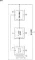
(撮像装置のICチップの構成例)
図10乃至図13は、撮像装置11がIC(Integrated Circuit)チップに形成される場合のICチップの構成例を示す図である。(Configuration example of IC chip of imaging device)
FIGS. 10 to 13 are diagrams illustrating a configuration example of an IC chip when the
撮像装置11がICチップに形成される場合、例えば、図10に示すように、イメージセンサ23、ベイヤ化処理部24、および信号処理部25は、それぞれ異なるICチップ71,72,73に形成されるようにすることができる。 When the
また、図11に示すように、イメージセンサ23とベイヤ化処理部24が同一のICチップ81に形成され、信号処理部25が、ICチップ81とは異なるICチップ82に形成されるようにすることもできる。 Also, as shown in FIG. 11, the
さらに、図12に示すように、イメージセンサ23が1つのICチップ91に形成され、ベイヤ化処理部24と信号処理部25が、ICチップ91とは異なるICチップ92に形成されるようにすることもできる。また、図13に示すように、イメージセンサ23、ベイヤ化処理部24、および信号処理部25の全てが同一のICチップ101に形成されるようにすることもできる。 Further, as shown in FIG. 12, the
なお、レンズ21と光学フィルタ22は、イメージセンサ23が形成されるICチップ71(81,91,101)のイメージセンサ23上に形成される。 The
以上のように、撮像装置11は、非ベイヤ配列の撮像画像に対してベイヤ化処理を行う際、ベイヤ化処理前の撮像画像の低周波成分(W+IR)Lの信号レベルと、ベイヤ化処理後のRGB画像の緑色の画素の画素信号の信号レベルが同一になるように、可視光成分GWLの信号レベルを補正する。従って、撮像装置11は、既存のベイヤ配列の撮像画像用の信号処理部25を用いて、ベイヤ化処理後のRGB画像に基づいて露光制御を行うことにより、非ベイヤ配列の撮像画像の露光制御を適切に行うことができる。As described above, when the
また、撮像装置11は、イメージセンサ23により撮像された赤外光成分を含む非ベイヤ配列の撮像画像から赤外光成分を分離し、ベイヤ化処理を行う。従って、非ベイヤ配列の撮像画像が赤外光成分を含む場合であっても、撮像装置11は、既存のベイヤ配列の撮像画像用の信号処理部25を用いて、非ベイヤ配列の撮像画像の露光制御を適切に行うことができる。 Further, the
さらに、撮像装置11は、非ベイヤ配列の撮像画像に対してベイヤ化処理を行う際、ベイヤ化処理前の撮像画像の可視光成分RL,GL,BLの信号レベルの比と、ベイヤ化処理後のRGB画像の各色の画素信号の信号レベルの比が同一になるように、画素信号R,G,Bのホワイトバランスを制御する。従って、撮像装置11は、既存のベイヤ配列の撮像画像用の信号処理部25を用いて、ベイヤ化処理後のRGB画像に基づいてホワイトバランス制御を行うことにより、非ベイヤ配列の撮像画像のホワイトバランス制御を適切に行うことができる。Furthermore, when performing the Bayerization process on the captured image in the non-Bayer array, the
<第2実施の形態>
(撮像装置の第2実施の形態の構成例)
図14は、本開示を適用した撮像装置を含む撮像システムの第2実施の形態の構成例を示すブロック図である。<Second embodiment>
(Configuration Example of Second Embodiment of Imaging Apparatus)
FIG. 14 is a block diagram illustrating a configuration example of a second embodiment of an imaging system including an imaging device to which the present disclosure is applied.
図14に示す構成のうち、図1の構成と同じ構成には同じ符号を付してある。重複する説明については適宜省略する。 In the configuration shown in FIG. 14, the same components as those in FIG. 1 are denoted by the same reference numerals. Duplicate descriptions will be omitted as appropriate.
図14の撮像システム120の構成は、撮像装置11の代わりに撮像装置121が設けられる点が、図1の撮像システム10の構成と異なる。また、撮像装置121の構成は、ベイヤ化処理部24の代わりにベイヤ化処理部141が設けられる点、信号処理部25の代わりに信号処理部142が設けられる点が、図1の撮像装置11の構成と異なる。撮像装置121は、ベイヤ化処理部141において、信号処理部142のホワイトバランス制御処理で算出されたホワイトバランスゲインを用いる。 The configuration of the
具体的には、撮像装置121のベイヤ化処理部141は、イメージセンサ23から供給される非ベイヤ配列の撮像画像に対してベイヤ化処理を行い、ベイヤ配列のRGB画像を生成する。このとき、ベイヤ化処理部141は、信号処理部142から供給されるホワイトバランスゲインを用いてホワイトバランスを補正し、元に戻す。ベイヤ化処理部141は、生成されたベイヤ配列のRGB画像を信号処理部142に供給する。 Specifically, the
信号処理部142は、既存のベイヤ配列の撮像画像用の信号処理部である。信号処理部142は、ベイヤ化処理部141から供給されるRGB画像を用いて、ベイヤ配列の撮像画像に対する方法と同一の方法で、露光制御処理、ホワイトバランス制御処理、YCbCr変換処理などの信号処理を行う。信号処理部142は、露光制御処理の結果得られる露光量を表すシャッタゲインをイメージセンサ23に供給し、撮像画像の露光量を制御する。 The
また、信号処理部142は、ホワイトバランス制御処理において算出されたホワイトバランスゲインをベイヤ化処理部141に供給する。さらに、信号処理部142は、ホワイトバランス制御処理およびYCbCr変換処理の結果得られるYCbCr画像を出力する。 In addition, the
(ベイヤ化処理部の構成例)
図15は、図14のベイヤ化処理部141の構成例を示すブロック図である。(Configuration example of Bayerization processing unit)
FIG. 15 is a block diagram illustrating a configuration example of the
図15に示す構成のうち、図4の構成と同じ構成には同じ符号を付してある。重複する説明については適宜省略する。 In the configuration shown in FIG. 15, the same components as those in FIG. 4 are denoted by the same reference numerals. Duplicate descriptions will be omitted as appropriate.
図15のベイヤ化処理部141の構成は、ゲイン算出部43、ホワイトバランス部44、逆ホワイトバランス部54の代わりに、ゲイン算出部161、ホワイトバランス部162、逆ホワイトバランス部163が設けられる点が、図4のベイヤ化処理部24の構成と異なる。 The configuration of the
ベイヤ化処理部141のゲイン算出部161は、図4のゲイン算出部43と同様に、分離部42から供給される可視光成分GLと、低周波処理部41から供給される低周波成分(W+IR)Lとに基づいて、上述した式(3)により、補正ゲインCEを算出する。ゲイン算出部161は、補正ゲインCEをレベル補正部45に供給する。しかしながら、ゲイン算出部161は、ゲイン算出部43のように、ホワイトバランスゲインCWR,CWG,CWBや、その逆数を算出しない。The
ホワイトバランス部162は、分離部42から供給される可視光成分RL,GL、およびBLのそれぞれに対して、図4のホワイトバランス部44と同様に、図14の信号処理部142から供給されるホワイトバランスゲインを乗算し、可視光成分RL,GL、およびBLの比率を補正する。ホワイトバランス部162は、補正後の可視光成分RWL,GWL、およびBWLをレベル補正部45に供給する。White balance unit 162, the visible light component RL supplied from
逆ホワイトバランス部163(ホワイトバランス制御部)は、図1の信号処理部142から供給されるホワイトバランスゲインの逆数を算出する。逆ホワイトバランス部163は、高周波復元処理部53から供給される画素信号R,G,Bに対して、算出されたホワイトバランスゲインの逆数をそれぞれ乗算する。これにより、イメージセンサ23から出力されたベイヤ化処理前の撮像画像の1画面内の赤色、緑色、および青色の画素信号の信号レベルの平均値の比と、ベイヤ化処理部141から出力されるベイヤ化処理後のRGB画像の1画面内の赤色、緑色、および青色の画素信号の信号レベルの平均値の比が同一になるように、画素信号R,G,Bのホワイトバランスが制御される。逆ホワイトバランス部163は、ホワイトバランスが制御された画素信号R,G,Bをベイヤ化部55に供給する。 The inverse white balance unit 163 (white balance control unit) calculates the reciprocal of the white balance gain supplied from the
(撮像装置の処理の説明)
図16および図17は、図14の撮像装置121の撮像処理を説明するフローチャートである。この撮像処理は、例えば、イメージセンサ23の撮像画像単位で行われる。(Description of processing of imaging apparatus)
FIGS. 16 and 17 are flowcharts illustrating the imaging process of the
図16のステップS51乃至S54の処理は、図8のステップS11乃至S14の処理と同様であるので、説明は省略する。 The processing in steps S51 to S54 in FIG. 16 is the same as the processing in steps S11 to S14 in FIG. 8, and a description thereof will be omitted.
ステップS55において、ベイヤ化処理部141のホワイトバランス部162(図15)は、信号処理部142から供給されるホワイトバランスゲインを取得する。なお、先頭の撮像画像に対する撮像処理では、まだホワイトバランスゲインが算出されていないため、ステップS55において、例えば、予め決められたホワイトバランスゲインのデフォルト値が、取得されたホワイトバランスゲインとされる。 In step S55, the white balance unit 162 (FIG. 15) of the
ステップS56の処理は、図8のステップS17の処理と同様であるので、説明は省略する。ステップS57において、ホワイトバランス部162は、分離部42から供給される可視光成分RL,GL、およびBLのそれぞれに対して、取得されたホワイトバランスゲインを乗算する。ホワイトバランス部44は、乗算後の可視光成分RWL,GWL、およびBWLをレベル補正部45に供給する。The process in step S56 is the same as the process in step S17 in FIG. 8, and a description thereof will not be repeated. In step S57, the white balance unit 162 multiplies each of the visible light components RL , GL , and BL supplied from the
ステップS58乃至S67の処理は、図8および図9のステップS19乃至S28の処理と同様であるので、説明は省略する。 The processing in steps S58 to S67 is the same as the processing in steps S19 to S28 in FIGS. 8 and 9, and a description thereof will be omitted.
ステップS68において、逆ホワイトバランス部163は、信号処理部142から供給されるホワイトバランスゲインを取得し、その逆数を算出する。なお、先頭の撮像画像に対する撮像処理では、まだホワイトバランスゲインが算出されていないため、ステップS68において、例えば、予め決められたホワイトバランスゲインのデフォルト値が、取得されたホワイトバランスゲインとされ、その逆数が算出される。 In step S68, the inverse
ステップS69において、逆ホワイトバランス部163は、高周波復元処理部53から供給される画素信号R,G,Bに対して、算出されたホワイトバランスゲインの逆数を乗算し、ベイヤ化部55に供給する。 In step S69, the inverse
ステップS70およびS71の処理は、図9のステップS30およびS31の処理と同様であるので、説明は省略する。 The processing in steps S70 and S71 is the same as the processing in steps S30 and S31 in FIG. 9, and a description thereof will be omitted.
ステップS72において、信号処理部142は、ベイヤ配列のRGB画像に基づいてホワイトバランス制御処理を行う。また、信号処理部142は、ホワイトバランス制御処理により算出されたホワイトバランスゲインを、ホワイトバランス部162と逆ホワイトバランス部163に供給する。 In step S72, the
ステップS73の処理は、図9のステップS33の処理と同様であるので、説明は省略する。 The process in step S73 is the same as the process in step S33 in FIG.
なお、第2実施の形態においても、第1実施の形態と同様に、撮像装置121をICチップに形成することができる。 Note that also in the second embodiment, the
<非ベイヤ配列の他の例>
本技術は、赤外光成分を含むRGBW画素配列の撮像画像以外の非ベイヤ配列の撮像画像に対してベイヤ化処理を行う画像処理装置にも適用することができる。ベイヤ化処理の対象となる撮像画像には、赤外光成分が含まれていてもよいし、含まれていなくてもよい。<Other examples of non-Bayer array>
The present technology can also be applied to an image processing apparatus that performs a Bayerization process on a captured image in a non-Bayer array other than a captured image in an RGBW pixel array including an infrared light component. The captured image to be subjected to the Bayer processing may or may not include an infrared light component.
図18は、RGBW画素配列以外の非ベイヤ配列の例を示す図である。 FIG. 18 is a diagram illustrating an example of a non-Bayer array other than the RGBW pixel array.
図18のAの画素配列は、RGB+IR画素配列であり、各画素が、赤色(R)の光、緑色(G)の光、青色(B)の光、および赤外光(IR)のいずれかに対応する画像を撮像する。図18のBの画素配列は、補色W画素配列であり、各画素が、白色(W)、黄色(Ye)、シアン(Cy)、および緑色(G)の光のいずれかに対応する画像を撮像する。 The pixel array of FIG. 18A is an RGB + IR pixel array, and each pixel has red (R) light, green (G) light, blue (B) light, and infrared light (IR). An image corresponding to any one is captured. The pixel array B in FIG. 18 is a complementary-color W pixel array, and each pixel represents an image corresponding to one of white (W), yellow (Ye), cyan (Cy), and green (G) light. Take an image.
ベイヤ化処理の内容は、非ベイヤ配列の種類、非ベイヤ配列の撮像画像に赤外光成分が含まれているかどうか等によって異なる。従って、例えば、ベイヤ化処理において、RGB信号をYCbCr信号に変換する処理や赤外光成分を分離する処理が行われない場合がある。また、ベイヤ化処理部は、ホワイトバランス部44と逆ホワイトバランス部54を備えない場合もある。 The content of the Bayer processing differs depending on the type of the non-Bayer array, whether or not the captured image of the non-Bayer array includes an infrared light component, and the like. Therefore, for example, in the Bayer processing, processing for converting an RGB signal into a YCbCr signal or processing for separating an infrared light component may not be performed. Further, the Bayer processing section may not include the white balance section 44 and the reverse
しかしながら、ベイヤ化処理を行う際、ベイヤ化処理前の撮像画像の最も感度の高い画素の信号レベルと、ベイヤ化処理後の画像の露光制御に用いられる画素の信号レベルが同一になるように、撮像画像の信号レベルが補正される。従って、信号処理部25(142)は、ベイヤ配列の撮像画像の露光制御方法で、非ベイヤ配列の撮像画像の露光制御を行うことができる。 However, when performing the Bayerization process, the signal level of the pixel with the highest sensitivity of the captured image before the Bayerization process is the same as the signal level of the pixel used for exposure control of the image after the Bayerization process, The signal level of the captured image is corrected. Therefore, the signal processing unit 25 (142) can control the exposure of the captured image of the non-Bayer array by the exposure control method of the captured image of the Bayer array.
<第3実施の形態>
(本開示を適用したコンピュータの説明)
上述した一連の処理は、ハードウエアにより実行することもできるし、ソフトウエアにより実行することもできる。一連の処理をソフトウエアにより実行する場合には、そのソフトウエアを構成するプログラムが、コンピュータにインストールされる。ここで、コンピュータには、専用のハードウエアに組み込まれているコンピュータや、各種のプログラムをインストールすることで、各種の機能を実行することが可能な、例えば汎用のパーソナルコンピュータなどが含まれる。<Third embodiment>
(Description of computer to which the present disclosure is applied)
The above-described series of processes can be executed by hardware or can be executed by software. When a series of processing is executed by software, a program constituting the software is installed in a computer. Here, the computer includes a computer incorporated in dedicated hardware, a general-purpose personal computer that can execute various functions by installing various programs, and the like.
図19は、上述した一連の処理をプログラムにより実行するコンピュータのハードウエアの構成例を示すブロック図である。 FIG. 19 is a block diagram illustrating a configuration example of hardware of a computer that executes the series of processes described above by a program.
コンピュータ200において、CPU(Central Processing Unit)201,ROM(Read Only Memory)202,RAM(Random Access Memory)203は、バス204により相互に接続されている。 In the
バス204には、さらに、入出力インタフェース205が接続されている。入出力インタフェース205には、撮像部206、入力部207、出力部208、記憶部209、通信部210、及びドライブ211が接続されている。 The
撮像部206は、レンズ21、光学フィルタ22、イメージセンサ23などにより構成され、撮像を行う。入力部207は、キーボード、マウス、マイクロフォンなどよりなる。出力部208は、ディスプレイ、スピーカなどよりなる。記憶部209は、ハードディスクや不揮発性のメモリなどよりなる。通信部210は、ネットワークインタフェースなどよりなる。ドライブ211は、磁気ディスク、光ディスク、光磁気ディスク、又は半導体メモリなどのリムーバブルメディア212を駆動する。 The
以上のように構成されるコンピュータ200では、CPU201が、例えば、記憶部209に記憶されているプログラムを、入出力インタフェース205及びバス204を介して、RAM203にロードして実行することにより、上述した一連の処理が行われる。 In the
コンピュータ200(CPU201)が実行するプログラムは、例えば、パッケージメディア等としてのリムーバブルメディア212に記録して提供することができる。また、プログラムは、ローカルエリアネットワーク、インターネット、デジタル衛星放送といった、有線または無線の伝送媒体を介して提供することができる。 The program executed by the computer 200 (CPU 201) can be provided by being recorded on a
コンピュータ200では、プログラムは、リムーバブルメディア212をドライブ211に装着することにより、入出力インタフェース205を介して、記憶部209にインストールすることができる。また、プログラムは、有線または無線の伝送媒体を介して、通信部210で受信し、記憶部209にインストールすることができる。その他、プログラムは、ROM202や記憶部209に、あらかじめインストールしておくことができる。 In the
なお、コンピュータ200が実行するプログラムは、本明細書で説明する順序に沿って時系列に処理が行われるプログラムであっても良いし、並列に、あるいは呼び出しが行われたとき等の必要なタイミングで処理が行われるプログラムであっても良い。 Note that the program executed by the
本明細書において、システムとは、複数の構成要素(装置、モジュール(部品)等)の集合を意味し、すべての構成要素が同一筐体中にあるか否かは問わない。したがって、別個の筐体に収納され、ネットワークを介して接続されている複数の装置、及び、1つの筐体の中に複数のモジュールが収納されている1つの装置は、いずれも、システムである。 In this specification, a system means a set of a plurality of components (devices, modules (parts), and the like), and it does not matter whether all components are in the same housing. Therefore, a plurality of devices housed in separate housings and connected via a network and one device housing a plurality of modules in one housing are all systems. .
また、本明細書に記載された効果はあくまで例示であって限定されるものではなく、他の効果があってもよい。 Further, the effects described in the present specification are merely examples and are not limited, and other effects may be provided.
さらに、本開示の実施の形態は、上述した実施の形態に限定されるものではなく、本開示の要旨を逸脱しない範囲において種々の変更が可能である。 Furthermore, the embodiments of the present disclosure are not limited to the above-described embodiments, and various changes can be made without departing from the gist of the present disclosure.
例えば、信号処理部25は、ベイヤ配列の撮像画像の露光制御方法にしたがう露光制御として、輝度信号に基づく露光制御を行うようにしてもよい。この場合、ゲイン算出部43は、可視光成分RL,GL、およびBLから輝度信号の1画面内の平均値を生成し、平均値Ave(W+IR)Lを輝度信号の平均値で除算することにより、補正ゲインCEを算出する。For example, the
なお、本開示は、以下のような構成もとることができる。 Note that the present disclosure may have the following configurations.
(1)
非ベイヤ配列の撮像画像に対してベイヤ化処理を行う際、ベイヤ化処理前の前記撮像画像の最も感度の高い画素の信号レベルである前レベルと、ベイヤ化処理後の前記撮像画像の、ベイヤ配列の画像の露光制御に用いられる画素の信号レベルである後レベルが同一になるように、前記撮像画像の信号レベルを補正するレベル補正部
を備える撮像装置。
(2)
前記前レベルと前記後レベルに基づいて、前記前レベルと前記後レベルを同一にするために前記撮像画像の信号レベルに乗算する補正ゲインを算出する補正ゲイン算出部
をさらに備え、
前記レベル補正部は、前記補正ゲイン算出部により算出された前記補正ゲインを、前記撮像画像の信号レベルに乗算する
ように構成された
前記(1)に記載の撮像装置。
(3)
前記非ベイヤ配列の撮像画像に対してベイヤ化処理を行う際、ベイヤ化処理前の前記撮像画像のRGBの信号レベルの比と、ベイヤ化処理後の前記撮像画像のRGBの信号レベルの比が同一になるように、前記撮像画像のホワイトバランスを制御するホワイトバランス制御部
をさらに備える
前記(1)または(2)に記載の撮像装置。
(4)
前記非ベイヤ配列の撮像画像に対してベイヤ化処理を行う際、前記撮像画像に対してホワイトバランスゲインを乗算するホワイトバランス部
をさらに備え、
前記ホワイトバランス制御部は、前記ホワイトバランス部により前記ホワイトバランスゲインが乗算された前記撮像画像に対して、前記ホワイトバランスゲインの逆数を乗算することにより、前記撮像画像のホワイトバランスを制御する
ように構成された
前記(3)に記載の撮像装置。
(5)
前記非ベイヤ配列の撮像画像に対してベイヤ化処理を行う際、前記撮像画像に基づいて前記ホワイトバランスゲインを算出するホワイトバランスゲイン算出部
をさらに備える
前記(4)に記載の撮像装置。
(6)
前記ホワイトバランスゲインは、前記ベイヤ化処理後の撮像画像を用いて所定の信号処理を行う際に算出される
ように構成された
前記(4)に記載の撮像装置。
(7)
前記非ベイヤ配列の撮像画像の各画素の信号には、不可視光成分と可視光成分が含まれる
ように構成された
前記(1)乃至(6)のいずれかに記載の撮像装置。
(8)
前記信号に含まれる前記不可視光成分と前記可視光成分を分離する分離部
をさらに備え、
前記レベル補正部は、前記分離部により分離された前記可視光成分の信号レベルを補正する
ように構成された
前記(7)に記載の撮像装置。
(9)
撮像装置が、
非ベイヤ配列の撮像画像に対してベイヤ化処理を行う際、ベイヤ化処理前の前記撮像画像の最も感度の高い画素の信号レベルである前レベルと、ベイヤ化処理後の前記撮像画像の、ベイヤ配列の画像の露光制御に用いられる画素の信号レベルである後レベルが同一になるように、前記撮像画像の信号レベルを補正するレベル補正ステップ
を含む撮像方法。
(10)
コンピュータを、
非ベイヤ配列の撮像画像に対してベイヤ化処理を行う際、ベイヤ化処理前の前記撮像画像の最も感度の高い画素の信号レベルである前レベルと、ベイヤ化処理後の前記撮像画像の、ベイヤ配列の画像の露光制御に用いられる画素の信号レベルである後レベルが同一になるように、前記撮像画像の信号レベルを補正するレベル補正部
として機能させるためのプログラム。(1)
When performing a Bayerization process on a captured image of a non-Bayer array, a Bayer image of the captured image after the Bayerization process includes a previous level that is a signal level of a pixel having the highest sensitivity of the captured image before the Bayerization process. An imaging apparatus comprising: a level correction unit that corrects a signal level of the captured image so that a subsequent level that is a signal level of a pixel used for exposure control of an image in the array is the same.
(2)
A correction gain calculator configured to calculate a correction gain by which a signal level of the captured image is multiplied to make the front level and the rear level the same based on the front level and the rear level,
The imaging device according to (1), wherein the level correction unit is configured to multiply the signal level of the captured image by the correction gain calculated by the correction gain calculation unit.
(3)
When performing the Bayerization process on the captured image of the non-Bayer array, the ratio of the RGB signal level of the captured image before the Bayerization process and the ratio of the RGB signal level of the captured image after the Bayerization process are different. The imaging device according to (1) or (2), further including a white balance control unit configured to control a white balance of the captured image so as to be the same.
(4)
When performing the Bayerization process on the captured image of the non-Bayer array, further comprising a white balance unit that multiplies the captured image by a white balance gain,
The white balance control unit controls a white balance of the captured image by multiplying the captured image multiplied by the white balance gain by the white balance unit by a reciprocal of the white balance gain. The imaging device according to (3).
(5)
The imaging device according to (4), further including: a white balance gain calculation unit configured to calculate the white balance gain based on the captured image when performing the Bayerization process on the captured image in the non-Bayer array.
(6)
The imaging device according to (4), wherein the white balance gain is calculated when predetermined signal processing is performed using the captured image after the Bayerization processing.
(7)
The imaging device according to any one of (1) to (6), wherein a signal of each pixel of the captured image in the non-Bayer array includes an invisible light component and a visible light component.
(8)
A separation unit that separates the invisible light component and the visible light component included in the signal.
The imaging device according to (7), wherein the level correction unit is configured to correct a signal level of the visible light component separated by the separation unit.
(9)
The imaging device is
When performing a Bayerization process on a captured image of a non-Bayer array, a Bayer image of the captured image after the Bayerization process includes a previous level that is a signal level of a pixel having the highest sensitivity of the captured image before the Bayerization process. A level correction step of correcting a signal level of the captured image so that a subsequent level which is a signal level of a pixel used for exposure control of an image in the array is the same.
(10)
Computer
When performing a Bayerization process on a captured image of a non-Bayer array, a Bayer image of the captured image after the Bayerization process includes a previous level that is a signal level of a pixel having the highest sensitivity of the captured image before the Bayerization process. A program for functioning as a level correction unit that corrects the signal level of the captured image so that the subsequent level, which is the signal level of the pixels used for exposure control of the arrayed images, is the same.
11 撮像装置, 42 分離部, 43 ゲイン算出部, 44 ホワイトバランス部, 45 レベル補正部, 54 逆ホワイトバランス部, 121 撮像装置, 162 ホワイトバランス部 11 imaging device, 42 separation unit, 43 gain calculation unit, 44 white balance unit, 45 level correction unit, 54 reverse white balance unit, 121 imaging device, 162 white balance unit
Claims (10)
Translated fromJapaneseを備える撮像装置。When performing a Bayerization process on a captured image of a non-Bayer array, a Bayer image of the captured image after the Bayerization process includes a previous level that is a signal level of a pixel having the highest sensitivity of the captured image before the Bayerization process. An imaging apparatus comprising: a level correction unit that corrects a signal level of the captured image so that a subsequent level that is a signal level of a pixel used for exposure control of an image in the array is the same.
をさらに備え、
前記レベル補正部は、前記補正ゲイン算出部により算出された前記補正ゲインを、前記撮像画像の信号レベルに乗算する
ように構成された
請求項1に記載の撮像装置。A correction gain calculator configured to calculate a correction gain by which a signal level of the captured image is multiplied to make the front level and the rear level the same based on the front level and the rear level,
The imaging apparatus according to claim 1, wherein the level correction unit is configured to multiply the signal level of the captured image by the correction gain calculated by the correction gain calculation unit.
をさらに備える
請求項1に記載の撮像装置。When performing the Bayerization process on the captured image of the non-Bayer array, the ratio of the RGB signal level of the captured image before the Bayerization process and the ratio of the RGB signal level of the captured image after the Bayerization process are different. The imaging device according to claim 1, further comprising a white balance control unit configured to control a white balance of the captured image so as to be the same.
をさらに備え、
前記ホワイトバランス制御部は、前記ホワイトバランス部により前記ホワイトバランスゲインが乗算された前記撮像画像に対して、前記ホワイトバランスゲインの逆数を乗算することにより、前記撮像画像のホワイトバランスを制御する
ように構成された
請求項3に記載の撮像装置。When performing the Bayerization process on the captured image of the non-Bayer array, further comprising a white balance unit that multiplies the captured image by a white balance gain,
The white balance control unit controls a white balance of the captured image by multiplying the captured image multiplied by the white balance gain by the white balance unit by a reciprocal of the white balance gain. The imaging device according to claim 3, which is configured.
をさらに備える
請求項4に記載の撮像装置。The imaging apparatus according to claim 4, further comprising: a white balance gain calculator that calculates the white balance gain based on the captured image when performing the Bayerization process on the captured image in the non-Bayer array.
ように構成された
請求項4に記載の撮像装置。The imaging device according to claim 4, wherein the white balance gain is calculated when predetermined signal processing is performed using the captured image after the Bayerization processing.
ように構成された
請求項1に記載の撮像装置。The imaging device according to claim 1, wherein a signal of each pixel of the captured image in the non-Bayer array includes an invisible light component and a visible light component.
をさらに備え、
前記レベル補正部は、前記分離部により分離された前記可視光成分の信号レベルを補正する
ように構成された
請求項7に記載の撮像装置。A separation unit that separates the invisible light component and the visible light component included in the signal.
The imaging device according to claim 7, wherein the level correction unit is configured to correct a signal level of the visible light component separated by the separation unit.
非ベイヤ配列の撮像画像に対してベイヤ化処理を行う際、ベイヤ化処理前の前記撮像画像の最も感度の高い画素の信号レベルである前レベルと、ベイヤ化処理後の前記撮像画像の、ベイヤ配列の画像の露光制御に用いられる画素の信号レベルである後レベルが同一になるように、前記撮像画像の信号レベルを補正するレベル補正ステップ
を含む撮像方法。The imaging device is
When performing a Bayerization process on a captured image of a non-Bayer array, a Bayer image of the captured image after the Bayerization process includes a previous level that is a signal level of a pixel having the highest sensitivity of the captured image before the Bayerization process. A level correction step of correcting a signal level of the captured image so that a subsequent level which is a signal level of a pixel used for exposure control of an image in the array is the same.
非ベイヤ配列の撮像画像に対してベイヤ化処理を行う際、ベイヤ化処理前の前記撮像画像の最も感度の高い画素の信号レベルである前レベルと、ベイヤ化処理後の前記撮像画像の、ベイヤ配列の画像の露光制御に用いられる画素の信号レベルである後レベルが同一になるように、前記撮像画像の信号レベルを補正するレベル補正部
として機能させるためのプログラム。Computer
When performing a Bayerization process on a captured image of a non-Bayer array, a Bayer image of the captured image after the Bayerization process includes a previous level that is a signal level of a pixel having the highest sensitivity of the captured image before the Bayerization process. A program for functioning as a level correction unit that corrects the signal level of the captured image so that the subsequent level, which is the signal level of the pixel used for exposure control of the array image, is the same.
Applications Claiming Priority (3)
| Application Number | Priority Date | Filing Date | Title |
|---|---|---|---|
| JP2014256045 | 2014-12-18 | ||
| JP2014256045 | 2014-12-18 | ||
| PCT/JP2015/084390WO2016098641A1 (en) | 2014-12-18 | 2015-12-08 | Image pickup device, image pickup method, and program |
Publications (2)
| Publication Number | Publication Date |
|---|---|
| JPWO2016098641A1 JPWO2016098641A1 (en) | 2017-09-28 |
| JP6643250B2true JP6643250B2 (en) | 2020-02-12 |
Family
ID=56126533
Family Applications (1)
| Application Number | Title | Priority Date | Filing Date |
|---|---|---|---|
| JP2016564799AExpired - Fee RelatedJP6643250B2 (en) | 2014-12-18 | 2015-12-08 | Imaging device, imaging method, and program |
Country Status (3)
| Country | Link |
|---|---|
| US (1) | US10110825B2 (en) |
| JP (1) | JP6643250B2 (en) |
| WO (1) | WO2016098641A1 (en) |
Cited By (1)
| Publication number | Priority date | Publication date | Assignee | Title |
|---|---|---|---|---|
| KR20220036014A (en)* | 2020-09-15 | 2022-03-22 | 삼성전자주식회사 | Image sensing system |
Families Citing this family (11)
| Publication number | Priority date | Publication date | Assignee | Title |
|---|---|---|---|---|
| WO2016047240A1 (en) | 2014-09-24 | 2016-03-31 | ソニー株式会社 | Image processing device, image pickup element, image pickup device, and image processing method |
| JP6732726B2 (en) | 2015-02-26 | 2020-07-29 | ソニーセミコンダクタソリューションズ株式会社 | Imaging device, imaging method, and program |
| CN106507080B (en)* | 2016-11-29 | 2018-07-17 | 广东欧珀移动通信有限公司 | Control method, control device and electronic device |
| JP7150514B2 (en)* | 2018-08-09 | 2022-10-11 | キヤノン株式会社 | Imaging device and imaging method |
| JP7253129B2 (en)* | 2019-01-07 | 2023-04-06 | ソニー・オリンパスメディカルソリューションズ株式会社 | Image processing device and observation system |
| TWI715142B (en)* | 2019-08-07 | 2021-01-01 | 瑞昱半導體股份有限公司 | Image sensing device and method for auto white balance therefor |
| KR20210104462A (en) | 2020-02-17 | 2021-08-25 | 삼성전자주식회사 | Image sensor, calibration method of image sensor, and electronic device for calibrating image sensor |
| JP7698377B2 (en)* | 2021-02-09 | 2025-06-25 | パナソニックオートモーティブシステムズ株式会社 | Vehicle imaging device, vehicle imaging method, vehicle imaging program, and moving body |
| US20240244334A1 (en)* | 2021-06-29 | 2024-07-18 | Sony Group Corporation | Image processing device, imaging device, and image processing method |
| CN113781303B (en) | 2021-09-01 | 2024-05-10 | 瑞芯微电子股份有限公司 | Image processing method, medium, processor and electronic device |
| EP4307702A4 (en)* | 2022-05-31 | 2024-08-21 | Samsung Electronics Co., Ltd. | ELECTRONIC DEVICE WITH IMAGE SENSOR AND OPERATING METHOD THEREFOR |
Family Cites Families (6)
| Publication number | Priority date | Publication date | Assignee | Title |
|---|---|---|---|---|
| JP2008289000A (en)* | 2007-05-18 | 2008-11-27 | Sony Corp | Image input processing device, and method thereof |
| JP4386096B2 (en) | 2007-05-18 | 2009-12-16 | ソニー株式会社 | Image input processing apparatus and method |
| JP5326943B2 (en)* | 2009-08-31 | 2013-10-30 | ソニー株式会社 | Image processing apparatus, image processing method, and program |
| EP2833635B1 (en)* | 2012-03-27 | 2018-11-07 | Sony Corporation | Image processing device, image-capturing element, image processing method, and program |
| JP2013219705A (en)* | 2012-04-12 | 2013-10-24 | Sony Corp | Image processor, image processing method and program |
| JP2016048815A (en)* | 2014-08-27 | 2016-04-07 | ソニー株式会社 | Image processor, image processing method and image processing system |
- 2015
- 2015-12-08JPJP2016564799Apatent/JP6643250B2/ennot_activeExpired - Fee Related
- 2015-12-08USUS15/534,679patent/US10110825B2/enactiveActive
- 2015-12-08WOPCT/JP2015/084390patent/WO2016098641A1/enactiveApplication Filing
Cited By (3)
| Publication number | Priority date | Publication date | Assignee | Title |
|---|---|---|---|---|
| KR20220036014A (en)* | 2020-09-15 | 2022-03-22 | 삼성전자주식회사 | Image sensing system |
| US12028637B2 (en) | 2020-09-15 | 2024-07-02 | Samsung Electronics Co., Ltd. | Image sensing system for converting an image signal to have a specific pattern |
| KR102791034B1 (en)* | 2020-09-15 | 2025-04-02 | 삼성전자주식회사 | Image sensing system |
Also Published As
| Publication number | Publication date |
|---|---|
| WO2016098641A1 (en) | 2016-06-23 |
| JPWO2016098641A1 (en) | 2017-09-28 |
| US10110825B2 (en) | 2018-10-23 |
| US20170366723A1 (en) | 2017-12-21 |
Similar Documents
| Publication | Publication Date | Title |
|---|---|---|
| JP6643250B2 (en) | Imaging device, imaging method, and program | |
| US10070104B2 (en) | Imaging systems with clear filter pixels | |
| US8547451B2 (en) | Apparatus and method for obtaining high dynamic range image | |
| US8467088B2 (en) | Image signal processing apparatus, imaging apparatus, image signal processing method and computer program | |
| CN101951457B (en) | Image processing apparatus and computer-readable medium | |
| US10699393B2 (en) | Image processing apparatus and image processing method | |
| JP6732726B2 (en) | Imaging device, imaging method, and program | |
| CN107534761B (en) | Imaging apparatus, imaging method, image processing apparatus | |
| WO2017098897A1 (en) | Imaging device, imaging control method, and program | |
| JP5223742B2 (en) | Edge-enhanced image processing apparatus | |
| US11889202B2 (en) | Image processing apparatus, image processing method, and storage medium | |
| CN107431793A (en) | Image processing apparatus and image processing method and program | |
| US20180288336A1 (en) | Image processing apparatus | |
| JP2010041174A (en) | Image processor | |
| CN111770321B (en) | Image processing apparatus, imaging apparatus, image processing method, and storage medium | |
| US8498494B2 (en) | Method and apparatus for processing a digital image signal, and a recording medium having recorded thereon a program for executing the method | |
| JP2006324789A (en) | Method and apparatus for processing video signal |
Legal Events
| Date | Code | Title | Description |
|---|---|---|---|
| A621 | Written request for application examination | Free format text:JAPANESE INTERMEDIATE CODE: A621 Effective date:20181015 | |
| TRDD | Decision of grant or rejection written | ||
| A01 | Written decision to grant a patent or to grant a registration (utility model) | Free format text:JAPANESE INTERMEDIATE CODE: A01 Effective date:20191210 | |
| A61 | First payment of annual fees (during grant procedure) | Free format text:JAPANESE INTERMEDIATE CODE: A61 Effective date:20200106 | |
| R150 | Certificate of patent or registration of utility model | Ref document number:6643250 Country of ref document:JP Free format text:JAPANESE INTERMEDIATE CODE: R150 | |
| LAPS | Cancellation because of no payment of annual fees |