JP6640696B2 - Interface system - Google Patents
Interface systemDownload PDFInfo
- Publication number
- JP6640696B2 JP6640696B2JP2016206337AJP2016206337AJP6640696B2JP 6640696 B2JP6640696 B2JP 6640696B2JP 2016206337 AJP2016206337 AJP 2016206337AJP 2016206337 AJP2016206337 AJP 2016206337AJP 6640696 B2JP6640696 B2JP 6640696B2
- Authority
- JP
- Japan
- Prior art keywords
- state
- host
- clock
- data
- interface system
- Prior art date
- Legal status (The legal status is an assumption and is not a legal conclusion. Google has not performed a legal analysis and makes no representation as to the accuracy of the status listed.)
- Active
Links
Images


Classifications
- H—ELECTRICITY
- H04—ELECTRIC COMMUNICATION TECHNIQUE
- H04L—TRANSMISSION OF DIGITAL INFORMATION, e.g. TELEGRAPHIC COMMUNICATION
- H04L7/00—Arrangements for synchronising receiver with transmitter
- H04L7/02—Speed or phase control by the received code signals, the signals containing no special synchronisation information
- H04L7/033—Speed or phase control by the received code signals, the signals containing no special synchronisation information using the transitions of the received signal to control the phase of the synchronising-signal-generating means, e.g. using a phase-locked loop
- G—PHYSICS
- G06—COMPUTING OR CALCULATING; COUNTING
- G06F—ELECTRIC DIGITAL DATA PROCESSING
- G06F1/00—Details not covered by groups G06F3/00 - G06F13/00 and G06F21/00
- G06F1/04—Generating or distributing clock signals or signals derived directly therefrom
- G06F1/06—Clock generators producing several clock signals
- G—PHYSICS
- G06—COMPUTING OR CALCULATING; COUNTING
- G06F—ELECTRIC DIGITAL DATA PROCESSING
- G06F13/00—Interconnection of, or transfer of information or other signals between, memories, input/output devices or central processing units
- G06F13/38—Information transfer, e.g. on bus
- G06F13/42—Bus transfer protocol, e.g. handshake; Synchronisation
- G06F13/4282—Bus transfer protocol, e.g. handshake; Synchronisation on a serial bus, e.g. I2C bus, SPI bus
- G06F13/4286—Bus transfer protocol, e.g. handshake; Synchronisation on a serial bus, e.g. I2C bus, SPI bus using a handshaking protocol, e.g. RS232C link
- G—PHYSICS
- G06—COMPUTING OR CALCULATING; COUNTING
- G06F—ELECTRIC DIGITAL DATA PROCESSING
- G06F1/00—Details not covered by groups G06F3/00 - G06F13/00 and G06F21/00
- G06F1/04—Generating or distributing clock signals or signals derived directly therefrom
- G06F1/12—Synchronisation of different clock signals provided by a plurality of clock generators
- G—PHYSICS
- G06—COMPUTING OR CALCULATING; COUNTING
- G06F—ELECTRIC DIGITAL DATA PROCESSING
- G06F1/00—Details not covered by groups G06F3/00 - G06F13/00 and G06F21/00
- G06F1/26—Power supply means, e.g. regulation thereof
- G06F1/32—Means for saving power
- G06F1/3203—Power management, i.e. event-based initiation of a power-saving mode
- G06F1/3234—Power saving characterised by the action undertaken
- G06F1/3237—Power saving characterised by the action undertaken by disabling clock generation or distribution
- G—PHYSICS
- G06—COMPUTING OR CALCULATING; COUNTING
- G06F—ELECTRIC DIGITAL DATA PROCESSING
- G06F13/00—Interconnection of, or transfer of information or other signals between, memories, input/output devices or central processing units
- G06F13/14—Handling requests for interconnection or transfer
- G06F13/16—Handling requests for interconnection or transfer for access to memory bus
- G06F13/1668—Details of memory controller
- G06F13/1689—Synchronisation and timing concerns
- G—PHYSICS
- G06—COMPUTING OR CALCULATING; COUNTING
- G06F—ELECTRIC DIGITAL DATA PROCESSING
- G06F13/00—Interconnection of, or transfer of information or other signals between, memories, input/output devices or central processing units
- G06F13/38—Information transfer, e.g. on bus
- G—PHYSICS
- G06—COMPUTING OR CALCULATING; COUNTING
- G06F—ELECTRIC DIGITAL DATA PROCESSING
- G06F13/00—Interconnection of, or transfer of information or other signals between, memories, input/output devices or central processing units
- G06F13/38—Information transfer, e.g. on bus
- G06F13/42—Bus transfer protocol, e.g. handshake; Synchronisation
- G06F13/4282—Bus transfer protocol, e.g. handshake; Synchronisation on a serial bus, e.g. I2C bus, SPI bus
- G06F13/4291—Bus transfer protocol, e.g. handshake; Synchronisation on a serial bus, e.g. I2C bus, SPI bus using a clocked protocol
- H—ELECTRICITY
- H03—ELECTRONIC CIRCUITRY
- H03L—AUTOMATIC CONTROL, STARTING, SYNCHRONISATION OR STABILISATION OF GENERATORS OF ELECTRONIC OSCILLATIONS OR PULSES
- H03L7/00—Automatic control of frequency or phase; Synchronisation
- H—ELECTRICITY
- H03—ELECTRONIC CIRCUITRY
- H03L—AUTOMATIC CONTROL, STARTING, SYNCHRONISATION OR STABILISATION OF GENERATORS OF ELECTRONIC OSCILLATIONS OR PULSES
- H03L7/00—Automatic control of frequency or phase; Synchronisation
- H03L7/06—Automatic control of frequency or phase; Synchronisation using a reference signal applied to a frequency- or phase-locked loop
- H03L7/07—Automatic control of frequency or phase; Synchronisation using a reference signal applied to a frequency- or phase-locked loop using several loops, e.g. for redundant clock signal generation
- H—ELECTRICITY
- H03—ELECTRONIC CIRCUITRY
- H03L—AUTOMATIC CONTROL, STARTING, SYNCHRONISATION OR STABILISATION OF GENERATORS OF ELECTRONIC OSCILLATIONS OR PULSES
- H03L7/00—Automatic control of frequency or phase; Synchronisation
- H03L7/06—Automatic control of frequency or phase; Synchronisation using a reference signal applied to a frequency- or phase-locked loop
- H03L7/08—Details of the phase-locked loop
- H03L7/0807—Details of the phase-locked loop concerning mainly a recovery circuit for the reference signal
- H—ELECTRICITY
- H03—ELECTRONIC CIRCUITRY
- H03L—AUTOMATIC CONTROL, STARTING, SYNCHRONISATION OR STABILISATION OF GENERATORS OF ELECTRONIC OSCILLATIONS OR PULSES
- H03L7/00—Automatic control of frequency or phase; Synchronisation
- H03L7/06—Automatic control of frequency or phase; Synchronisation using a reference signal applied to a frequency- or phase-locked loop
- H03L7/08—Details of the phase-locked loop
- H03L7/085—Details of the phase-locked loop concerning mainly the frequency- or phase-detection arrangement including the filtering or amplification of its output signal
- H03L7/091—Details of the phase-locked loop concerning mainly the frequency- or phase-detection arrangement including the filtering or amplification of its output signal the phase or frequency detector using a sampling device
- H—ELECTRICITY
- H03—ELECTRONIC CIRCUITRY
- H03L—AUTOMATIC CONTROL, STARTING, SYNCHRONISATION OR STABILISATION OF GENERATORS OF ELECTRONIC OSCILLATIONS OR PULSES
- H03L7/00—Automatic control of frequency or phase; Synchronisation
- H03L7/06—Automatic control of frequency or phase; Synchronisation using a reference signal applied to a frequency- or phase-locked loop
- H03L7/08—Details of the phase-locked loop
- H03L7/099—Details of the phase-locked loop concerning mainly the controlled oscillator of the loop
- H—ELECTRICITY
- H04—ELECTRIC COMMUNICATION TECHNIQUE
- H04L—TRANSMISSION OF DIGITAL INFORMATION, e.g. TELEGRAPHIC COMMUNICATION
- H04L25/00—Baseband systems
- H04L25/02—Details ; arrangements for supplying electrical power along data transmission lines
- H04L25/08—Modifications for reducing interference; Modifications for reducing effects due to line faults ; Receiver end arrangements for detecting or overcoming line faults
- H04L25/085—Arrangements for reducing interference in line transmission systems, e.g. by differential transmission
- H—ELECTRICITY
- H04—ELECTRIC COMMUNICATION TECHNIQUE
- H04L—TRANSMISSION OF DIGITAL INFORMATION, e.g. TELEGRAPHIC COMMUNICATION
- H04L25/00—Baseband systems
- H04L25/02—Details ; arrangements for supplying electrical power along data transmission lines
- H04L25/14—Channel dividing arrangements, i.e. in which a single bit stream is divided between several baseband channels and reassembled at the receiver
- H—ELECTRICITY
- H04—ELECTRIC COMMUNICATION TECHNIQUE
- H04L—TRANSMISSION OF DIGITAL INFORMATION, e.g. TELEGRAPHIC COMMUNICATION
- H04L7/00—Arrangements for synchronising receiver with transmitter
- H04L7/0004—Initialisation of the receiver
- H—ELECTRICITY
- H04—ELECTRIC COMMUNICATION TECHNIQUE
- H04L—TRANSMISSION OF DIGITAL INFORMATION, e.g. TELEGRAPHIC COMMUNICATION
- H04L7/00—Arrangements for synchronising receiver with transmitter
- H04L7/0008—Synchronisation information channels, e.g. clock distribution lines
- H04L7/0012—Synchronisation information channels, e.g. clock distribution lines by comparing receiver clock with transmitter clock
- Y—GENERAL TAGGING OF NEW TECHNOLOGICAL DEVELOPMENTS; GENERAL TAGGING OF CROSS-SECTIONAL TECHNOLOGIES SPANNING OVER SEVERAL SECTIONS OF THE IPC; TECHNICAL SUBJECTS COVERED BY FORMER USPC CROSS-REFERENCE ART COLLECTIONS [XRACs] AND DIGESTS
- Y02—TECHNOLOGIES OR APPLICATIONS FOR MITIGATION OR ADAPTATION AGAINST CLIMATE CHANGE
- Y02D—CLIMATE CHANGE MITIGATION TECHNOLOGIES IN INFORMATION AND COMMUNICATION TECHNOLOGIES [ICT], I.E. INFORMATION AND COMMUNICATION TECHNOLOGIES AIMING AT THE REDUCTION OF THEIR OWN ENERGY USE
- Y02D10/00—Energy efficient computing, e.g. low power processors, power management or thermal management
Landscapes
- Engineering & Computer Science (AREA)
- Theoretical Computer Science (AREA)
- Computer Networks & Wireless Communication (AREA)
- Signal Processing (AREA)
- General Physics & Mathematics (AREA)
- General Engineering & Computer Science (AREA)
- Physics & Mathematics (AREA)
- Power Engineering (AREA)
- Stabilization Of Oscillater, Synchronisation, Frequency Synthesizers (AREA)
- Synchronisation In Digital Transmission Systems (AREA)
- Power Sources (AREA)
- Information Transfer Systems (AREA)
- Communication Control (AREA)
- Selective Calling Equipment (AREA)
Description
Translated fromJapanese実施形態は、インターフェースシステムに関する。 Embodiments relate to an interface system.
UHS-II/-IIIは、例えば、メモリカードのホストインターフェース規格として使用され、差動シリアル結合による高速伝送方式を標準化する。一方、メモリカードは、リムーバブルデバイスであることから、メモリカードの電極とソケットの電極との物理的なコンタクトによりホストとの電気的接続を確保する。 UHS-II / -III is used, for example, as a host interface standard of a memory card, and standardizes a high-speed transmission method by differential serial coupling. On the other hand, since the memory card is a removable device, electrical connection with the host is secured by physical contact between the electrode of the memory card and the electrode of the socket.
実施形態は、待機電力が小さく、かつ、高速復帰が可能なインターフェースシステムを提案する。 The embodiment proposes an interface system that has a small standby power and can return at high speed.
実施形態によれば、ホストに接続可能なインターフェースシステムは、前記ホストからの第1のクロック及びシリアルデータを受信する受信機と、第1のVCOを含み、前記第1のクロックに基づいて第2のクロックを生成する第1のクロックジェネレータと、第2のVCOを含み、前記シリアルデータに基づいて第3のクロックを生成する第2のクロックジェネレータと、前記第3のクロック及び前記シリアルデータに基づいて受信データをサンプリングするサンプリング回路と、前記第1及び第2のクロックジェネレータが動作状態である第1の状態及び前記第1及び第2のクロックジェネレータが非動作状態である第2の状態を制御するコントローラと、を備える。前記第1のクロック及び前記シリアルデータは、前記第1の状態において前記受信機に供給され、前記第2の状態において前記受信機に供給されない。前記コントローラは、第1の復帰モードにおいて、前記第2の状態から前記第1の状態に変化することを確認してから一定期間が経過した後に前記受信データのサンプリング又は前記ホストへの送信データの伝送を開始し、前記第2及び第3のクロックが同期したことを示す応答を前記ホストに転送しない。According to an embodiment, an interface system connectable to a host includes a receiver for receiving a first clock and serial data from the host, and a first VCO, and a second VCO based on the first clock. A second clock generator that generates a third clock based on the serial data, and a second clock generator that generates athird clock based on the serial data. A first circuit in which the first and second clock generators are in operation and a second state in which the first and second clock generators are inoperative. And a controller that performs the operation. The first clock and the serial data are provided to the receiver in the first state and are not provided to the receiver in the second state. In the first return mode, the controller may sample the reception data or transmit the transmission data to the host after a predetermined period has elapsed after confirming that the state changes from the second state to the first state. Initiate transmission and do not forward a response to the host indicating that the second and third clocks are synchronized.
(実施例)
以下、図面を参照しながら実施例を説明する。(Example)
Hereinafter, embodiments will be described with reference to the drawings.
図1は、インターフェースシステムの例を示している。 FIG. 1 shows an example of the interface system.
ホスト10は、コントローラ11と、コントローラ11により制御されるデバイスインターフェース12と、を備える。デバイス20は、コントローラ21と、コントローラ21により制御されるホストインターフェース22と、を備える。 The
デバイス20は、メモリカードなどのリムーバブルデバイスである。デバイス20は、リムーバブルデバイスであるため、ホスト10との電気的接続が物理的なコンタクトにより確保される。このため、デバイス20は、高周波伝送に不向きであり、かつ、ホスト10とのコンタクト状態が不安定に成り易い。 The
そこで、例えば、インターフェース規格としてのUHS-II/-III規格においては、デバイスインターフェース12とホストインターフェース22は、リファレンスクロック伝送路30及びデータ伝送路31,32を備える。これら伝送路30,31,32は、差動信号を伝送可能なように、信号線ペア(Lane+, Lane-)を備える。 Therefore, for example, in the UHS-II / -III standard as the interface standard, the
そして、ホスト10は、データ伝送路31,32によるシリアルデータD0,D1の伝送と並行して、リファレンスクロック伝送路30によりリファレンスクロックRCLKをデバイス20に供給する。リファレンスクロックRCLKは、低速(低周波数)のクロックであり、デバイス20は、リファレンスクロックRCLKに基づいて、データ受信やデータ送信などを高速に行うための高周波数の内部クロックを生成する。 Then, the
このように、UHS-II/-III規格では、デバイス20がリファレンスクロックRCLKに基づいて内部クロックを生成することにより、EMI(Electro-magnetic interference)を低減し、かつ、送受信データの伝送の効率化を図る。 As described above, in the UHS-II / -III standard, the
しかし、例えば、UHS-II規格では、リファレンスクロックRCLKの周波数は、データ伝送レート(周波数)の1/15又は1/30と規定され、かつ、UHS-III規格では、リファレンスクロックRCLKの周波数は、データ伝送レートの1/60又は1/120と規定される。 However, for example, in the UHS-II standard, the frequency of the reference clock RCLK is defined as 1/15 or 1/30 of the data transmission rate (frequency), and in the UHS-III standard, the frequency of the reference clock RCLK is It is defined as 1/60 or 1/120 of the data transmission rate.
従って、例えば、デバイス20をリセット状態又は休止状態からアクティブ状態に変化させる場合、このような低周波数のリファレンスクロックRCLKに基づいて内部クロックを生成しようとすると、リファレンスクロックRCLKを受けてから内部クロックの周波数が安定するまでの時間、例えば、リファレンスクロックRCLKを受けてからPLL(Phase-locked loop)回路の出力周波数がロックされるまでの時間が長くなり、かつ、その時間も安定しない(ばらつきが大きくなる)。 Therefore, for example, when changing the
尚、デバイス20がリセット状態であるとは、デバイス20がホスト10から物理的に切り離されている状態、例えば、メモリカードがソケットから抜き取られている状態を意味する。 Note that the
また、デバイス20が休止状態であるとは、デバイス20がホスト10に物理的に接続されている状態、例えば、メモリカードがソケットに挿入されている状態において、デバイス20がパワーセーブモードにエンターしている状態(送受信データの伝送が不可能な状態)を意味する。 In addition, the
さらに、デバイス20がアクティブ状態であるとは、デバイス20がホスト10に物理的に接続されている状態、例えば、メモリカードがソケットに挿入されている状態において、デバイス20が通常動作モードにエンターしている状態(送受信データの伝送が可能な状態)を意味する。 Further, the
この場合、ホスト10とデバイス20との間で送受信データの伝送を開始するためには、ホスト10が、デバイス20において送受信データの伝送の準備が完了したこと、即ち、内部クロックの周波数が安定したことを確認する必要がある。内部クロックの周波数が安定すること、例えば、PLL回路の出力周波数がロックされることは、内部クロックが同期する、と称される。また、内部クロックが同期したことを確認することは、ホスト10とデバイス20との間のハンドシェークチェック(又はリンクチェック)と称される。 In this case, in order to start transmission of transmission / reception data between the
ホスト10とデバイス20との間においてハンドシェークチェックを行うためには、デバイス20は、例えば、データ伝送路32を用いて、内部クロックが同期したことを示す応答をホスト10に伝送しなければならない。結果として、ハンドシェークチェックのために、さらなる時間を要し、データ伝送のレイテンシを長くしてしまう。 In order to perform a handshake check between the
一方、UHS-II規格では、ローパワーモード(Low power mode)と呼ばれる仕様が存在する。この仕様では、例えば、休止状態においても、リファレンスクロックRCLKがホスト10からデバイス20に供給されるため、デバイス20において、内部クロックは、常に安定した状態にある。 On the other hand, the UHS-II standard has a specification called a low power mode. In this specification, for example, even in the sleep state, the reference clock RCLK is supplied from the
従って、例えば、デバイス20が休止状態からアクティブ状態に変化する場合、ハンドシェークチェックを行わなくても、休止状態からアクティブ状態への変化を指示されてから一定期間が経過すれば、ホスト10とデバイス20との間で送受信データの伝送を行うことができる。この一定期間は、休止状態においてリファレンスクロックRCLKの供給を停止する場合に送受信データの伝送が可能となるまでの時間に比べて、非常に短い。即ち、データ伝送のレイテンシを短くできる。 Therefore, for example, when the
しかし、このローパワーモードでは、例えば、内部クロックを生成するPLL回路は、デバイス20が休止状態にあっても、動作状態でなければならない。このため、休止状態でのデバイス20の消費電力が大きくなってしまう。 However, in this low power mode, for example, the PLL circuit that generates the internal clock must be in operation even when the
そこで、以下の実施例では、デバイス20が休止状態に変化する場合にリファレンスクロックRCLKの供給を停止し、かつ、デバイス20がアクティブ状態に復帰する場合にホスト10とデバイス20との間のハンドシェークチェックを省略する新たなモードを追加することにより、休止状態での待機電力が小さく、かつ、休止状態からアクティブ状態への高速復帰が可能なインターフェースシステムを提案する。 Therefore, in the following embodiment, the supply of the reference clock RCLK is stopped when the
尚、コントローラ21内の第1及び第2のレジスタREG0、REG.1については、以下の図2において説明する。 The first and second registers REG0, REG. 1 will be described with reference to FIG. 2 below.
図2は、ホストインターフェースの例を示している。 FIG. 2 shows an example of the host interface.
伝送路30,31,32は、例えば、UHS-II/-III規格などの高速シリアルインタフェース規格に準拠する。この規格では、例えば、リファレンスクロックRCLKは、リファレンスクロック伝送路30を経由して、ホストインターフェース22に入力される。また、シリアルデータD0は、データ伝送路31を経由してホストインターフェース22に入力され、シリアルデータD1は、データ伝送路32を経由して、ホストに出力される。 The
ホストインターフェース22は、例えば、受信機23と、PLL回路(クロックジェネレータ)24と、CDR(Clock data recovery)回路(クロックジェネレータ)25と、サンプリング回路26と、送信器27と、を備える。 The
受信機23は、差動アンプ231,232を備える。差動アンプ231は、リファレンスクロックRCLKの入力バッファとして機能し、差動アンプ232は、シリアルデータD0の入力バッファとして機能する。 The
差動アンプ231は、差動信号としてのリファレンスクロックRCLKを単層信号(シングルエンド信号)に変換し、これをPLL回路24に出力する。差動アンプ232は、差動信号としてのシリアルデータD0を単層信号に変換し、これをCDR回路25及びサンプリング回路26に出力する。 The
PLL回路24は、リファレンスクロックRCLKに基づいて、内部クロックCLK0を生成する。内部クロックCLK0は、例えば、送信機27に出力される。送信機27は、内部クロックCLK0に基づいて、送信データDOUTをシリアルデータD1としてデータ伝送路32に出力する。 The
また、PLL回路24は、VCO(Voltage-controlled oscillator)を備える。VCOは、制御電圧V0により制御される。本例では、制御電圧V0は、CDR回路25にも出力される。 Further, the
CDR回路25は、シリアルデータD0に基づいて、内部クロックCLK1を生成する。CDR回路25は、PLL回路でもある。内部クロックCLK1は、例えば、サンプリング回路26に出力される。サンプリング回路26は、内部クロックCLK1に基づいて、シリアルデータD0から受信データDINを抽出する。内部クロックCLK1は、高速データ受信を可能とするため、リファレンスクロックRCLKからではなく、シリアルデータD0から生成される。 The
PLL回路24及びCDR回路25は、例えば、デバイスがパワーセーブモードにエンターしているとき、内部クロックCLK0,CLK1を出力しない待機状態に変化することが可能である。PLL回路24及びCDR回路25が待機状態にあることにより、ホスト及びデバイス間で送受信データの伝送が行われていない期間における電力を削減できる。これについては、後述する。 For example, when the device is in the power save mode, the
ここで、図1のレジスタREG.0,REG.1について説明する。 Here, the register REG. 0, REG. 1 will be described.
レジスタREG.0は、例えば、Device Capabilities Registerと呼ばれ、レジスタREG.1は、例えば、Device Setting Registerと呼ばれる。 Register REG. 0 is called, for example, a Device Capabilities Register, and the register REG. 1 is called, for example, a Device Setting Register.
レジスタREG.0は、例えば、図2のPLL回路24及びCDR回路25が動作可能となるパラメータを記憶する。 Register REG. 0 stores, for example, a parameter at which the
例えば、内部クロックCLK1の同期に必要な期間T_EIDL_RECOVERYは、レジスタREG.0内に記憶される。この期間は、例えば、STBL信号の長さ、又は、STBL信号が一定の長さを有する場合はSTBL信号の数(シンボル数)で規定される。レジスタREG.0は、STBH信号とSTBL信号との間のEIDL信号の期間又はシンボル数を記憶してもよい。 For example, the period T_EIDL_RECOVERY necessary for synchronizing the internal clock CLK1 is set in the register REG. Stored in 0. This period is defined by, for example, the length of the STBL signal, or the number of STBL signals (the number of symbols) when the STBL signal has a fixed length. Register REG. 0 may store the period or the number of symbols of the EIDL signal between the STBH signal and the STBL signal.
また、レジスタREG.1は、例えば、図2のPLL回路24及びCDR回路25を動作させるうえで必要なパラメータを記憶する。例えば、このパラメータ(N_EIDL_RECOVERY_GAP、T_EIDL_RECOVERY、T_EIDL_GAPなどの値)は、図2のPLL回路24及びCDR回路25の周波数レンジなどによって変わる。 The register REG. 1 stores, for example, parameters necessary for operating the
図1のコントローラ21は、レジスタREG.0,REG1内に記憶されたパラメータ(内部クロックCLK0,CLK1の同期などに必要な時間)に従ってホストインターフェース22を制御する。 The
図3は、PLL回路及びCDR回路の例を示している。 FIG. 3 shows an example of the PLL circuit and the CDR circuit.
PLL回路24は、位相比較器241と、チャージポンプ回路242と、ループフィルタ243と、VCO244と、分周器245と、動作制御ユニット246と、制御電圧記憶ユニット247と、を備える。 The
位相比較器241は、リファレンスクロックRCLKの位相と、分周器245からのフィードバッククロックFCLKの位相と、を比較する。位相比較器241は、両クロックの位相差に相当する制御信号(アップ信号及びダウン信号)を出力する。 The
例えば、リファレンスクロックRCLKの周波数がフィードバッククロックFCLKの周波数より高い場合、位相比較器241は、フィードバッククロックFCLKの周波数を高くするアップ信号を出力する。また、リファレンスクロックRCLKの周波数がフィードバッククロックFCLKの周波数よりも低い場合、位相比較器241は、フィードバッククロックFCLKの周波数を低くするダウン信号を出力する。 For example, when the frequency of the reference clock RCLK is higher than the frequency of the feedback clock FCLK, the
チャージポンプ回路242は、位相比較器241からの制御信号(アップ信号及びダウン信号)をチャージポンプ電流(アナログ信号)に変換し、これをループフィルタ243に出力する。ループフィルタ243は、チャージポンプ電流を制御電圧V0に変換する。VCO244は、制御電圧V0に基づいて、内部クロックCLK0を出力する。分周器245は、内部クロックCLK0の周波数の1/Nの周波数を有するフィードバッククロックFCLKを出力する。 The
即ち、PLL回路24は、リファレンスクロックRCLKの周波数のN倍の周波数を有する内部クロックCLK0を生成する。但し、Nは、1以上の自然数である。また、Nは、送受信データのデータ転送レートに応じて、複数の値から選択可能であってもよい。 That is, the
また、内部クロックCLK0の周波数がリファレンスクロックRCLKの周波数のN倍よりも低い場合、リファレンスクロックRCLKの周波数は、フィードバッククロックFCLKの周波数よりも高くなる。従って、位相比較器241は、アップ信号を出力し、VCO244は、内部クロックCLK0の周波数を高くする。 When the frequency of the internal clock CLK0 is lower than N times the frequency of the reference clock RCLK, the frequency of the reference clock RCLK becomes higher than the frequency of the feedback clock FCLK. Therefore, the
一方、内部クロックCLK0の周波数がリファレンスクロックRCLKの周波数のN倍よりも高い場合、リファレンスクロックRCLKの周波数は、フィードバッククロックFCLKの周波数よりも低くなる。従って、位相比較器241は、ダウン信号を出力し、VCO244は、内部クロックCLK0の周波数を低くする。 On the other hand, when the frequency of the internal clock CLK0 is higher than N times the frequency of the reference clock RCLK, the frequency of the reference clock RCLK becomes lower than the frequency of the feedback clock FCLK. Therefore, the
このような制御により、内部クロックCLK0の周波数は、最終的に、リファレンスクロックRCLKの周波数のN倍にロックされる。内部クロックCLK0の周波数がロックされた状態は、内部クロックCLK0が同期した状態であり、かつ、ホストとデバイスとの間で送受信データの伝送が可能となる状態である。 By such control, the frequency of the internal clock CLK0 is finally locked to N times the frequency of the reference clock RCLK. The state where the frequency of the internal clock CLK0 is locked is a state where the internal clock CLK0 is synchronized and a state where transmission / reception data can be transmitted between the host and the device.
動作制御ユニット246は、例えば、デバイスがパワーセーブモードにエンターしているとき、例えば、PLL回路24を動作状態から待機状態に変化させる。但し、パワーセーブモードにエンターしても、PLL回路24を動作状態のままにしておいてもよい。ここで、動作状態とは、内部クロックCLK0を出力可能な状態であり、待機状態とは、内部クロックCLK0を出力しない状態である。 The
本例では、動作制御ユニット246は、待機状態において、領域Xで囲まれるチャージポンプ回路242、ループフィルタ243、VCO244、及び、分周器245を、それぞれ非動作状態に変化させる。これにより、ホスト及びデバイス間で送受信データの伝送が行われていない期間において、インターフェースシステムの消費電力が削減される。 In this example, in the standby state, the
位相比較器241は、例えば、デバイスがホストに物理的に接続されている状態において常に動作状態である。従って、動作制御ユニット246は、位相比較器241からの制御信号φ0に基づいて、チャージポンプ回路242、ループフィルタ243、VCO244、及び、分周器245の動作を制御可能である。 The
例えば、制御信号φ0が、リファレンスクロックRCLKが入力されていないことを示す場合、動作制御ユニット246は、チャージポンプ回路242、ループフィルタ243、VCO244、及び、分周器245を、非動作状態に変化させる。また、制御信号φ0が、リファレンスクロックRCLKが入力されていることを示す場合、動作制御ユニット246は、チャージポンプ回路242、ループフィルタ243、VCO244、及び、分周器245を、動作状態に変化させる。 For example, when the control signal φ0 indicates that the reference clock RCLK is not input, the
制御電圧記憶ユニット247は、内部クロックCLK0の周波数がロックされた場合、即ち、内部クロックCLK0が同期した場合、ロック状態のVCO244に入力される制御電圧V0を記憶する。この制御電圧V0は、この後、デバイスがパワーセーブモードにエンターし、さらに、パワーセーブモードから通常動作モードに復帰するときに、内部クロックCLK0の周波数を高速にロックするために使用される。 When the frequency of the internal clock CLK0 is locked, that is, when the internal clock CLK0 is synchronized, the control
即ち、パワーセーブモードの前後においては、送受信データのデータ転送レート(レンジ)の変更は無いと考えることができる。この場合、パワーセーブモード後の通常動作モードにおいて、内部クロックCLKの周波数がロックされる制御電圧V0は、パワーセーブモード前の通常動作モードにおいて、内部クロックCLKの周波数がロックされた制御電圧V0、又は、それに近い値を有すると想定できる。 That is, it can be considered that there is no change in the data transfer rate (range) of the transmission / reception data before and after the power save mode. In this case, the control voltage V0 in which the frequency of the internal clock CLK is locked in the normal operation mode after the power save mode is the control voltage V0 in which the frequency of the internal clock CLK is locked in the normal operation mode before the power save mode. Or it can be assumed that it has a value close to it.
従って、パワーセーブモードから通常動作モードに復帰した場合、パワーセーブモード前の通常動作モードにおいて、内部クロックCLKの周波数がロックされた制御電圧V0を、VCO244の初期制御電圧(VCO244が動作状態に変化したときの最初の制御電圧)とすれば、例えば、VCO244の初期制御電圧が0Vである場合に比べて、内部クロックCLK0の周波数を高速にロックできる。 Therefore, when returning from the power save mode to the normal operation mode, in the normal operation mode before the power save mode, the control voltage V0 in which the frequency of the internal clock CLK is locked is changed to the initial control voltage of the VCO 244 (
但し、これは、パワーセーブモードから通常動作モードへの復帰の場合のように、送受信データのデータ転送レート(レンジ)の変更が無いことを前提とする。 However, this is based on the assumption that there is no change in the data transfer rate (range) of transmission / reception data as in the case of returning from the power save mode to the normal operation mode.
即ち、インターフェースシステムにおいては、送受信データのデータ転送レートを変更するモードが存在する。このような場合には、データ転送レートを変更する前のVCO244の制御電圧V0を用いて、データ転送レートを変更した後のVCO244の出力周波数を高速にロックするというアルゴリズムは採用できない。 That is, in the interface system, there is a mode for changing the data transfer rate of the transmission / reception data. In such a case, it is not possible to employ an algorithm that uses the control voltage V0 of the
CDR回路25は、位相比較器251と、チャージポンプ回路252と、ループフィルタ253と、VCO254と、動作制御ユニット255と、を備える。 The
位相比較器251は、シリアルデータD0の位相と、VCO244からの内部クロック(フィードバッククロック)CLK1の位相と、を比較する。位相比較器251は、両クロックの位相差に相当する制御信号(アップ信号及びダウン信号)を出力する。 The
例えば、シリアルデータD0の周波数が内部クロックCLK1の周波数より高い場合、位相比較器251は、内部クロックCLK1の周波数を高くするアップ信号を出力する。また、シリアルデータD0の周波数が内部クロックCLK1の周波数よりも低い場合、位相比較器251は、内部クロックCLK1の周波数を低くするダウン信号を出力する。 For example, when the frequency of the serial data D0 is higher than the frequency of the internal clock CLK1, the
チャージポンプ回路252は、位相比較器251からの制御信号(アップ信号及びダウン信号)をチャージポンプ電流(アナログ信号)に変換し、これをループフィルタ253に出力する。ループフィルタ253は、チャージポンプ電流を制御電圧V1に変換する。VCO254は、制御電圧V1に基づいて、内部クロックCLK1を出力する。即ち、CDR回路25は、シリアルデータD0に同期した内部クロックCLK1を生成する。 The
また、内部クロックCLK1の周波数がシリアルデータD0の周波数よりも低い場合(シリアルデータD0の周波数が内部クロックCLK1の周波数よりも高い場合)、位相比較器251は、アップ信号を出力し、VCO254は、内部クロックCLK1の周波数を高くする。 When the frequency of the internal clock CLK1 is lower than the frequency of the serial data D0 (when the frequency of the serial data D0 is higher than the frequency of the internal clock CLK1), the
一方、内部クロックCLK1の周波数がシリアルデータD0の周波数よりも高い場合(シリアルデータD0の周波数が内部クロックCLK1の周波数よりも低い場合)、位相比較器251は、ダウン信号を出力し、VCO254は、内部クロックCLK1の周波数を低くする。 On the other hand, when the frequency of internal clock CLK1 is higher than the frequency of serial data D0 (when the frequency of serial data D0 is lower than the frequency of internal clock CLK1),
このような制御により、内部クロックCLK1の周波数は、最終的に、シリアルデータD0の周波数にロックされる。内部クロックCLK1の周波数がロックされた状態は、内部クロックCLK1が同期した状態であり、かつ、ホストとデバイスとの間で送受信データの伝送が可能となる状態である。 By such control, the frequency of the internal clock CLK1 is finally locked to the frequency of the serial data D0. The state where the frequency of the internal clock CLK1 is locked is a state where the internal clock CLK1 is synchronized and a state where transmission / reception data can be transmitted between the host and the device.
動作制御ユニット255は、例えば、デバイスがパワーセーブモードにエンターしているとき、例えば、CDR回路25を動作状態から待機状態に変化させる。但し、パワーセーブモードにエンターしても、CDR回路25を動作状態のままにしておいてもよい。 The
本例では、動作制御ユニット255は、待機状態において、領域Yで囲まれるチャージポンプ回路252、ループフィルタ253、及び、VCO254を、それぞれ非動作状態に変化させる。これにより、ホスト及びデバイス間で送受信データの伝送が行われていない期間において、インターフェースシステムの消費電力が削減される。 In the present example, the
位相比較器251は、例えば、デバイスがホストに物理的に接続されている状態において常に動作状態である。従って、動作制御ユニット255は、位相比較器251からの制御信号φ1に基づいて、チャージポンプ回路252、ループフィルタ253、及び、VCO254の動作を制御可能である。 The
例えば、制御信号φ1が、シリアルデータD0が入力されていないことを示す場合、動作制御ユニット255は、チャージポンプ回路252、ループフィルタ253、及び、VCO254を、非動作状態に変化させる。また、制御信号φ1が、シリアルデータD0が入力されていることを示す場合、動作制御ユニット255は、チャージポンプ回路252、ループフィルタ253、及び、VCO254を、動作状態に変化させる。 For example, when the control signal φ1 indicates that the serial data D0 has not been input, the
動作制御ユニット255は、VCO254を動作させる場合、PLL回路24の制御電圧V0を、初期制御電圧(VCO254が動作状態に変化したときの最初の制御電圧)として、VCO254に供給する。 When operating the
従って、パワーセーブモードから通常動作モードに復帰した場合、VCO254の初期制御電圧は、PLL回路24内のVCO244の制御電圧V0、又は、制御電圧記憶ユニット247からの初期制御電圧となるため、例えば、VCO254の初期制御電圧が0Vである場合に比べて、内部クロックCLK1の周波数を高速にロックできる。 Therefore, when returning from the power save mode to the normal operation mode, the initial control voltage of the
図4Aは、制御電圧記憶ユニットの例を示している。 FIG. 4A shows an example of the control voltage storage unit.
制御電圧記憶ユニット247は、カウンタレジスタ247aと、DAC(Digital-analog converter)247bと、差動アンプ(コンパレータ)247cと、スイッチ素子SWと、を備える。 The control
カウンタレジスタ247aは、VCO244の初期制御電圧(デジタル値)VC_0を記憶する。初期制御電圧VC_0は、例えば、製品出荷時、デフォルト値として記憶される。また、ホストとデバイスとの間で送受信データの伝送が行われた場合、カウンタレジスタ247aは、現時点の直前の通常動作モードにおいて、カウンタレジスタ247aが記憶したVCO244のロック時の制御電圧を、初期制御電圧VC_0として記憶する。 The
例えば、パワーセーブモードから通常動作モードに変化する場合、スイッチ素子SWは、オン状態に変化する。また、カウンタレジスタ247a内に記憶された初期制御電圧(デジタル値)VC_0は、DAC247bによりアナログ値に変換され、かつ、制御電圧V0としてVCO244に供給される。 For example, when changing from the power save mode to the normal operation mode, the switch element SW changes to the ON state. The initial control voltage (digital value) VC_0 stored in the
その結果、VCO244の出力周波数がロックされるまで、即ち、内部クロックCLK0が同期するまでのロックアップタイムは、大幅に短縮される。また、このロックアップタイムは、安定的である。これは、例えば、デバイスがパワーセーブモードから通常動作モードにエンターすることを確認してから一定期間内に、内部クロックCLK0が確実に同期することを意味する。 As a result, the lock-up time until the output frequency of the
スイッチ素子SWは、初期制御電圧VC_0をVCO244に供給した後、オフ状態に変化する。スイッチ素子SWをオフ状態にするタイミングは、初期制御電圧VC_0をVCO244に供給した後であればよい。例えば、スイッチ素子SWをオフ状態にするタイミングは、内部クロックCLK0が確実に同期する上述の一定期間より前であってもよいし、それより後であってもよい。 The switch element SW changes to the off state after supplying the initial control voltage VC_0 to the
スイッチ素子SWがオフ状態に変化すると、ループフィルタ243からの制御電圧V0は、例えば、差動アンプ247cのプラス入力端子に入力される。また、カウンタレジスタ247a内に記憶された初期制御電圧VC_0は、DAC247bを経由して、例えば、差動アンプ247cのマイナス入力端子に入力される。 When the switch element SW changes to the off state, the control voltage V0 from the
そして、図4Bに示すように、制御電圧V0が初期制御電圧VC_0よりも大きい場合、差動アンプ247cは、アップ信号(+)を出力する。アップ信号の値は、初期制御電圧VC_0と制御電圧V0との差に比例して大きくなる。カウンタレジスタ247aは、アップ信号の値に応じて、初期制御電圧VC_0を更新する、即ち、初期制御電圧VC_0を、アップ信号の値に応じたステップ数だけアップさせる。 Then, as shown in FIG. 4B, when the control voltage V0 is higher than the initial control voltage VC_0, the
また、図4Bに示すように、初期制御電圧VC_0が制御電圧V0よりも大きい場合、差動アンプ247cは、ダウン信号(−)を出力する。ダウン信号の値は、初期制御電圧VC_0と制御電圧V0との差に比例して大きくなる。カウンタレジスタ247aは、ダウン信号の値に応じて、初期制御電圧VC_0を更新する、即ち、初期制御電圧VC_0を、ダウン信号の値に応じたステップ数だけダウンさせる。 Further, as shown in FIG. 4B, when the initial control voltage VC_0 is higher than the control voltage V0, the
このような動作を繰り返すことで、DAC247bが出力する電圧は、ループフィルタ243からの制御電圧V0に追従する。最終的に、内部クロックCLK0の周波数(出力周波数)がロックされたときのループフィルタ243からの制御電圧V0が、更新された初期制御電圧VC_0として、カウンタレジスタ247a内に記憶される。 By repeating such an operation, the voltage output from the
尚、本例では、アップ/ダウン信号のステップ数は、VC_0とV0との差に比例するとしたが、差動アンプ247cをコンパレータとして動作させ、1ステップずつ、VC_を変化させてもよい。この場合、カウンタレジスタ247a内に記憶されるVC_0の値は、差動アンプ247cからのアップ/ダウン信号(±1)に応じて、1ステップずつ変化する。このようにしても、DAC247bが出力する電圧は、ループフィルタ243からの制御電圧V0に追従することになる。 In this example, the number of steps of the up / down signal is assumed to be proportional to the difference between VC_0 and V0. However, the
以上の制御電圧記憶ユニット247によれば、カウンタレジスタ247a内に記憶される初期制御電圧VC_0の値がループフィルタ243からの制御電圧V0に追従して更新される。このようなシステムにすれば、リファレンスクロックRCLKの周波数が異なる複数のインターフェースシステムに、本実施例を適用することが可能となる。即ち、初期制御電圧VC_0が固定値である場合や、複数の固定値から選択する場合など、は、リファレンスクロックRCLKの周波数が任意であるシステムに適用することは難しい。 According to the above control
尚、初期制御電圧VC_0は、カウンタレジスタ247aとは異なる記憶回路、例えば、SRAM、DRAMなどの揮発性RAMや、MRAMなどの不揮発性RAMに記憶してもよいし、ラッチ回路などに記憶してもよい。また、初期制御電圧VC_0は、デジタル値として記憶してもよいし、アナログ値として記憶してもよい。 Note that the initial control voltage VC_0 may be stored in a storage circuit different from the
このように、図2乃至図4に示す実施例によれば、パワーセーブモード前後のように、送受信データのデータ転送レート(レンジ)が変更されない場合においては、PLL回路24内のVCO244の初期制御電圧は、制御電圧記憶ユニット247内に記憶されるパワーセーブモード前のロック電圧(VCO244の出力周波数がロックされたときの制御電圧)VC_0である。また、CDR回路25内のVCO254の初期制御電圧は、PLL回路24内のVCO244の制御電圧V0、又は、制御電圧記憶ユニット247からのロック電圧VC_0である。 As described above, according to the embodiment shown in FIGS. 2 to 4, when the data transfer rate (range) of the transmission / reception data is not changed, such as before and after the power save mode, the initial control of the
これにより、例えば、図5に示すように、PLL回路24の出力周波数がロックされるまで、即ち、内部クロックCLK0が同期するまでのロックアップタイム(実施例T0〜T1)は、比較例T0〜T2に比べて、大幅に短縮される。また、パワーセーブモード後のロック電圧Bがパワーセーブモード前のロック電圧Aと異なる場合、実施例でのロックアップタイムのばらつきΔ0は、比較例でのロックアップタイムのばらつきΔ1よりも小さい。これは、実施例では、PLL回路24のロックアップタイムが高速かつ安定していることを意味する。 Thereby, for example, as shown in FIG. 5, the lock-up time until the output frequency of the
従って、後述するように、デバイスが休止状態に変化する場合にリファレンスクロックRCLKの供給を停止し、かつ、デバイスがアクティブ状態に復帰する場合にホスト及びデバイス間のハンドシェークを省略する新たなモードを追加することが可能となる。即ち、PLL回路24のロックアップタイムが高速かつ安定しているため、デバイスがアクティブ状態に復帰する場合、アクティブ状態への復帰を確認してから一定期間が経過したら直ちに、送受信データの伝送を行うことができる。 Therefore, as described later, a new mode is added in which the supply of the reference clock RCLK is stopped when the device changes to the sleep state and the handshake between the host and the device is omitted when the device returns to the active state. It is possible to do. That is, since the lock-up time of the
また、例えば、図6に示すように、CDR回路25の出力周波数がロックされるまで、即ち、内部クロックCLK1が同期するまでのロックアップタイム(実施例T0〜T3)も、比較例T0〜T4に比べて、大幅に短縮される。 Further, for example, as shown in FIG. 6, the lock-up time until the output frequency of the
これにより、待機電力が小さく、かつ、高速復帰が可能なインターフェースシステムを実現できる。 As a result, an interface system with low standby power and capable of high-speed recovery can be realized.
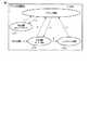
図7は、デバイスの状態変化を示している。 FIG. 7 shows a state change of the device.
デバイスの状態は、図1のコントローラ21により制御又は管理される。 The state of the device is controlled or managed by the
リセット状態、休止状態、及び、アクティブ状態については、図1において既に説明したので、ここでの説明を省略する。リンクチェック状態とは、図1乃至図6で説明したPLL回路24により生成される内部クロックCLK0の同期、及び、CDR回路25により生成される内部クロックCLK1の同期がそれぞれ完了したか、をチェックする状態を意味する。 The reset state, the pause state, and the active state have already been described with reference to FIG. The link check state is to check whether the synchronization of the internal clock CLK0 generated by the
本例では、休止状態が2種類存在する。 In this example, there are two types of sleep states.
休止状態S_d0は、例えば、パワーセーブモードにおいて、PLL回路24が内部クロックCLK0を生成し、かつ、CDR回路25が内部クロックCLK1を生成していない状態を意味する。即ち、休止状態S_d0では、リファレンスクロックRCLKは、ホストからデバイスに供給され、図1及び図2のリファレンスクロック伝送路30は、アクティブ状態にある。 The pause state S_d0 means, for example, a state in which the
例えば、休止状態S_d0では、図3のPLL回路24は、動作状態にあるが、図3のCDR回路25は、実質的に非動作状態にある。即ち、休止状態S_d0のCDR回路25において、位相比較器251は、動作状態であるが、領域Y内のチャージポンプ回路252、ループフィルタ253、及び、VCO254は、非動作状態である。また、シリアルデータD0は、ホストからデバイスに供給されておらず、図1及び図2のデータ伝送路31は、ノンアクティブ状態にある。 For example, in the sleep state S_d0, the
休止状態S_d1は、例えば、パワーセーブモードにおいて、PLL回路24が内部クロックCLK0を生成しておらず、かつ、CDR回路25も内部クロックCLK1を生成していない状態を意味する。即ち、休止状態S_d1では、リファレンスクロックRCLK及びシリアルデータD0は、ホストからデバイスに供給されておらず、図1及び図2のリファレンスクロック伝送路30及びデータ伝送路31は、共に、ノンアクティブ状態(EIDL: Electric idle)にある。 The sleep state S_d1 means, for example, a state in which the
例えば、休止状態S_d1では、図3のPLL回路24及びCDR回路25は、共に、実質的に非動作状態にある。即ち、休止状態S_d1のPLL回路24において、位相比較器241は、動作状態であるが、領域X内のチャージポンプ回路242、ループフィルタ243、及び、VCO244は、非動作状態である。また、休止状態S_d1のCDR回路25において、位相比較器251は、動作状態であるが、領域Y内のチャージポンプ回路252、ループフィルタ253、及び、VCO254は、非動作状態である。 For example, in the sleep state S_d1, both the
[リセット状態からアクティブ状態への変化]
図8は、リセット状態からアクティブ状態への変化の例を示している。[Change from reset state to active state]
FIG. 8 shows an example of a change from the reset state to the active state.
デバイス20がリセット状態(ホスト10から物理的に切り離された状態)からホスト物理的に接続された状態に変化すると、デバイス20は、休止状態S_d1となる。 When the
休止状態(時刻t0〜t1)S_d1では、伝送路30,31,32は、いずれもノンアクティブ状態(EIDL)である。例えば、伝送路30,31,32が、それぞれ、差動対としての信号線ペア(Lane+, Lane-)を備える場合、休止状態S_d1では、信号線ペア(Lane+, Lane-)は、例えば、共に、接地電圧Vssに設定される。 In the idle state (time t0 to t1) S_d1, the
まず、ホスト10は、デバイス20にアクティブ状態S_activeへの変化を指示するため、データ伝送路31にSTBL信号を出力する。また、ホスト10は、リファレンスクロック伝送路30にリファレンスクロックRCLKを出力する。 First, the
STBL信号は、例えば、データ伝送路31の信号線(Lane+)にロウレベル電圧が印加され、かつ、データ伝送路31の信号線(Lane-)にハイレベル電圧が印加されたDCレベル信号である。即ち、STBL信号は、Lane+にロウレベル電圧が印加されるストローブ(STB: Strobe)信号、及び、信号線ペア(Lane+, Lane-)の電圧が時間的に変化しない信号という意味である。 The STBL signal is, for example, a DC level signal in which a low-level voltage is applied to the signal line (Lane +) of the
デバイス20は、STBL信号を検出すると、アクティブ状態へ移行する前に、内部クロックCLK0の同期及び内部クロックCLK1の同期をそれぞれチェックするリンクチェック状態(時刻t1〜t2)S_linkに移行する(図7の経路B)。リンクチェック状態S_linkは、ホスト10とデバイス20との間で送受信データのデータ伝送が可能であるかをチェックするハンドシェークチェック状態とも称される。 Upon detecting the STBL signal, the
デバイス20は、内部クロックCLK0の同期が完了したことを確認すると、データ伝送路32にSTBL信号(ハンドシェークのための応答)を出力する。ホスト10は、デバイス20からデータ伝送路32を経由して転送されたSTBL信号を確認することにより、デバイス20において、内部クロックCLK0の同期が完了したことを確認できる。 When confirming that the synchronization of the internal clock CLK0 is completed, the
ホスト10は、STBL信号のハンドシェーク、即ち、内部クロックCLK0の同期が完了したことを確認した後、データ伝送路31にSYN信号を出力する。 The
SYN信号は、例えば、データ伝送路31の信号線ペア(Lane+, Lane-)の電圧がハイレベルとロウレベルの間で時間的に変化するACレベル信号である。SYN信号は、送受信データのデータ伝送の前提となる内部クロックCLK1の同期を完了するための同期信号(Synchronous signal)という意味である。 The SYN signal is, for example, an AC level signal in which the voltage of the signal line pair (Lane +, Lane-) of the
デバイス20は、SYN信号により内部クロックCLK1の同期が完了したことを確認すると、データ伝送路32にSYN信号(ハンドシェークのための応答)を出力する。ホスト10は、デバイス20からデータ伝送路32を経由して転送されたSYN信号を確認することにより、デバイス20において、内部クロックCLK1の同期が完了したことを確認できる。 When the
ホスト10が、デバイス20において内部クロックCLK0,CLK1の同期が完了したことを確認すると、デバイス20は、ホスト10とデバイス20の間で送受信データ(パケットデータ)PKTのデータ伝送が可能となるアクティブ状態S_activeとなる(図7の経路C)。 When the
[アクティブ状態及び休止状態間の変化]
図9は、アクティブ状態及び休止状態間の変化の例を示している。[Change between active state and dormant state]
FIG. 9 shows an example of a change between the active state and the dormant state.
同図において、A,B,C,D,A’,D’は、それぞれ、図7のステートマシーンにおける経路A,B,C,D,A’,D’に対応する。 7, A, B, C, D, A ', and D' correspond to paths A, B, C, D, A ', and D' in the state machine of FIG. 7, respectively.
図1乃至図6のインターフェースシステムにおいて、所定の条件が満たされたとき、デバイス20は、システムの消費電力を削減するため、通常動作モード(アクティブ状態)からパワーセーブモード(休止状態)に変化する。所定の条件とは、例えば、ホスト10とデバイス20との間で送受信データのデータ伝送が一定期間行われていな場合など、である。 In the interface system of FIGS. 1 to 6, when a predetermined condition is satisfied, the
所定の条件が満たされたとき、デバイス20は、パワーセーブモードに変化するが、所定の条件が満たされたか否かを判断するのは、ホスト10であってもよいし、又は、デバイス20であってもよい。ホスト10が所定の条件を満たしたと判断する場合、ホスト10は、パワーセーブモードに移行することを示すコマンドを、例えば、データ伝送路D0を用いて、デバイス20に転送する。 When the predetermined condition is satisfied, the
ここで重要な点は、本例のインターフェースシステムでは、既に説明したように、2種類の休止状態が存在することにある。一つは、図7の休止状態S_d0であり、他の一つは、図7の休止状態S_d1である。 The important point here is that, in the interface system of the present example, as described above, there are two types of sleep states. One is the sleep state S_d0 in FIG. 7, and the other is the sleep state S_d1 in FIG.
休止状態Sd_0は、リファレンスクロックRCLKがPLL回路24に供給され、かつ、PLL回路24が動作状態にある休止状態であり、UHS-II規格のローパワーモード(UHS-II規格では、休止状態とは異なる)に相当する。休止状態Sd_1は、リファレンスクロックRCLKがPLL回路24に供給されず、かつ、PLL回路24が非動作状態にあるため、UHS-II規格の休止状態(UHS-II規格では、休止状態は1つしか存在しない)に相当する。 The dormant state Sd_0 is a dormant state in which the reference clock RCLK is supplied to the
また、本発明のインターフェースシステムで重要な点は、休止状態S_d1からアクティブ状態S_activeに復帰する経路が2種類存在することにある。一つは、休止状態S_d1からアクティブ状態S_activeに直接復帰する経路であり(図7の経路D)、他の一つは、休止状態S_d1からリンクチェック状態S_linkを経由してアクティブ状態S_activeに復帰する経路である(図7の経路B→C)。 Also, what is important in the interface system of the present invention is that there are two types of paths for returning from the idle state S_d1 to the active state S_active. One is a path directly returning from the dormant state S_d1 to the active state S_active (path D in FIG. 7), and the other is returning from the dormant state S_d1 to the active state S_active via the link check state S_link. This is the route (route B → C in FIG. 7).
経路Dは、休止状態Sd_1において、リファレンスクロックRCLKがPLL回路24に供給されず、かつ、PLL回路24が非動作状態にあるにもかかわらず、リンクチェック状態S_linkを経由せずに、アクティブ状態S_activeに復帰する点で、図1乃至図6のインターフェースシステムに特徴的である。 The path D is in the active state S_active without passing through the link check state S_link even though the reference clock RCLK is not supplied to the
このような復帰が可能となるのは、図1乃至図6で既に説明したように、PLL回路24が、デバイス20がアクティブ状態への復帰を確認した後、一定期間内に、内部クロックCLK0を同期させる、即ち、内部クロックCLK0の周波数をロックさせることが可能であるからである。また、CDR回路25も、PLL回路24の制御電圧V0を利用して内部クロックCLK1を生成するため、上記一定期間内に、内部クロックCLK1を同期させる、即ち、内部クロックCLK1の周波数をロックさせることが可能である。 As described above with reference to FIGS. 1 to 6, such a return is possible because after the
即ち、図1乃至図6のインターフェースシステムでは、内部クロックCLK0,CLK1が上記一定期間内に確実に同期するため、リンクチェック、即ち、ホスト10とデバイス20との間のハンドシェークチェックを行わずに、休止状態S_d1からアクティブ状態S_activeに直接復帰することが可能となる。 That is, in the interface systems shown in FIGS. 1 to 6, since the internal clocks CLK0 and CLK1 are reliably synchronized within the above-mentioned fixed period, a link check, that is, a handshake check between the
尚、経路B→Cは、UHS-II規格の休止状態S_d1からアクティブ状態S_activeへの通常の復帰経路に相当する。 Note that the path B → C corresponds to a normal return path from the sleep state S_d1 of the UHS-II standard to the active state S_active.
以上をまとめると、図9に示すように、図1乃至図6のインターフェースシステムでは、3種類の復帰モードM0,M1,M2が存在することになる。 Summarizing the above, as shown in FIG. 9, in the interface systems of FIGS. 1 to 6, there are three types of return modes M0, M1, and M2.
これらモードの選択は、例えば、ホスト10がパワーセーブモードへのエンターをデバイス20に指示する場合、パワーセーブモードへのエンターを指示するコマンドに、復帰モードM0,M1,M2を指定するフラグQRを付加することにより行うことができる。ここでは、3種類の復帰モードM0,M1,M2が存在するため、フラグQRは、2ビットである。 For example, when the
例えば、フラグQRが01の場合、復帰モードM0が選択される。この場合、デバイス20は、アクティブ状態S_activeから休止状態間S_d0に変化し(経路A’)、この後、休止状態間S_d0からアクティブ状態S_activeに直接復帰する(経路D’)。 For example, when the flag QR is 01, the return mode M0 is selected. In this case, the
また、フラグQRが10の場合、復帰モードM1が選択される。この場合、デバイス20は、アクティブ状態S_activeから休止状態間S_d1に変化し(経路A)、この後、休止状態間S_d1からアクティブ状態S_activeに直接復帰する(経路D)。 When the flag QR is 10, the return mode M1 is selected. In this case, the
さらに、フラグQRが11の場合、復帰モードM2が選択される。この場合、デバイス20は、アクティブ状態S_activeから休止状態間S_d1に変化し(経路A)、この後、休止状態間S_d1から、リンクチェック状態S_linkを経由して、アクティブ状態S_activeに復帰する(経路B→D)。 Further, when the flag QR is 11, the return mode M2 is selected. In this case, the
[アクティブ状態から休止状態への変化]
図10A及び図10Bは、アクティブ状態から休止状態への変化の例を示している。[Change from active to hibernate]
10A and 10B show an example of a change from the active state to the dormant state.
デバイス20がアクティブ状態(時刻t3〜t4)S_activeの場合、伝送路30,31,32は、いずれもアクティブ状態である。リファレンスクロックRCLKは、ホスト10から、リファレンスクロック伝送路30を経由して、デバイス20に転送される。送受信データ(パケットデータ)PKTは、データ伝送路31,32により、ホスト10とデバイス20との間で転送される。 When the
アクティブ状態S_activeにおいて、ホスト10は、デバイス20に休止状態S_d0又はS_d1への変化を指示するため、データ伝送路31にコマンドGO_DSを出力する。続けて、ホスト10は、データ伝送路31にSTBH信号を出力する。 In the active state S_active, the
コマンドGO_DSは、休止状態S_d0又はS_d1への変化を指示すると共に、復帰モードM0,M1,M2のうちの1つを選択するフラグQRを含む。復帰モードM0,M1,M2の選択は、例えば、図11に示すように、パワーマネージメントに基づいて、行うことができる。 The command GO_DS includes a flag QR for instructing a change to the sleep state S_d0 or S_d1, and selecting one of the return modes M0, M1, and M2. The selection of the return mode M0, M1, M2 can be performed based on power management, for example, as shown in FIG.
図11の例では、インターフェースシステムの電源の状態が4種類存在する。 In the example of FIG. 11, there are four types of power states of the interface system.
D0状態は、例えば、インターフェースシステムの電源の全てがオンの状態であり、アクティブ状態S_activeに対応する。D1状態は、例えば、インターフェースシステムの電源の一部がオフの状態であり、休止状態S_d0に対応する。D2状態は、例えば、インターフェースシステムの電源の一部がオフの状態であり、休止状態S_d1に対応する。D3状態は、例えば、インターフェースシステムの電源の一部又は全てがオフの状態であり、休止状態S_d1に対応する。 The D0 state is, for example, a state where all the power supplies of the interface system are on, and corresponds to the active state S_active. The D1 state is, for example, a state in which part of the power supply of the interface system is off, and corresponds to the hibernate state S_d0. The D2 state is, for example, a state in which part of the power supply of the interface system is off, and corresponds to the sleep state S_d1. The D3 state is, for example, a state in which part or all of the power supply of the interface system is off, and corresponds to the sleep state S_d1.
インターフェースシステムの消費電力は、D0状態からD3状態に向かうに従い、次第に小さくなる。これに対し、休止状態S_d0又はS_d1からアクティブ状態S_activeへの復帰時間は、D0状態からD3状態に向かうに従い、次第に長くなる。即ち、消費電力と復帰時間は、トレードオフの関係にある。 The power consumption of the interface system gradually decreases from the D0 state to the D3 state. On the other hand, the return time from the dormant state S_d0 or S_d1 to the active state S_active gradually becomes longer from the D0 state to the D3 state. That is, the power consumption and the recovery time are in a trade-off relationship.
このトレードオフを考慮し、例えば、ホスト10内で使用されるオペレーティングシステム(OS)は、デバイス20を休止状態S_d0又はS_d1に移行させるに当たり、消費電力と復帰時間をパラメータとして、複数の復帰モードM0,M1,M2から最適なモードを選択する。また、オペレーティングシステムは、例えば、復帰モードM0をD1状態に対応付け、復帰モードM1をD2状態に対応付け、復帰モードM2をD3状態に対応付ける。 In consideration of this trade-off, for example, when the operating system (OS) used in the
ここで、復帰モードM1と復帰モードM2の違いについて説明する。 Here, the difference between the return mode M1 and the return mode M2 will be described.
復帰モードM1は、送受信データのデータ転送レート(レンジ)の変更を行わない場合に選択される。この場合、PLL回路及びCDR回路の出力周波数がロックされる制御電圧の大きな変更はない。従って、例えば、図3及び図4に示すような高速PLL回路24及び高速CDR回路25を用いることにより、一定期間での復帰が可能となり、復帰モードM1を選択することが可能となる。 The return mode M1 is selected when the data transfer rate (range) of the transmission / reception data is not changed. In this case, there is no significant change in the control voltage at which the output frequencies of the PLL circuit and the CDR circuit are locked. Therefore, for example, by using the high-
復帰モードM2は、送受信データのデータ転送レート(レンジ)の変更を行う場合に選択される。即ち、図1乃至図6のインターフェースシステムでは、PLL回路及びCDR回路の出力周波数(データ転送レート)を変更する場合がある。この場合、PLL回路及びCDR回路の出力周波数がロックされる制御電圧は、大きく変更される。従って、アクティブ状態への一定期間の復帰が不可能となるため、復帰モードM2を選択する。 The return mode M2 is selected when changing the data transfer rate (range) of transmission / reception data. That is, in the interface systems of FIGS. 1 to 6, the output frequencies (data transfer rates) of the PLL circuit and the CDR circuit may be changed. In this case, the control voltage at which the output frequencies of the PLL circuit and the CDR circuit are locked is greatly changed. Therefore, since it is impossible to return to the active state for a certain period, the return mode M2 is selected.
STBH信号は、例えば、データ伝送路31の信号線(Lane+)にハイレベル電圧が印加され、かつ、データ伝送路31の信号線(Lane-)にロウレベル電圧が印加されたDCレベル信号である。即ち、STBH信号は、Lane+にハイレベル電圧が印加されるストローブ(STB: Strobe)信号、及び、信号線ペア(Lane+, Lane-)の電圧が時間的に変化しない信号という意味である。 The STBH signal is, for example, a DC level signal in which a high-level voltage is applied to the signal line (Lane +) of the
デバイス20は、コマンドGO_DSを受け取った後、続けてSTBH信号を検出すると、休止状態S_d0又はS_d1へ移行する(図7の経路A又はA’)。また、デバイス20は、STBH信号を検出すると、データ伝送路32にSTBH信号(ホスト10からSTBH信号を受け取った旨の応答)を出力する。ホスト10は、デバイス20からデータ伝送路32を経由して転送されたSTBH信号を確認することにより、デバイス20が休止状態S_d0又はS_d1に移行したことを確認できる。 Upon receiving the command GO_DS and subsequently detecting the STBH signal, the
尚、LIDLは、データ伝送路32を用いたデータ伝送の同期を維持するための信号である。また、デバイス20は、コマンドGO_DSを受け取った後、データ伝送路32にコマンドGO_DS(コマンドGO_DSを受け取った旨の応答)を出力してもよい。 LIDL is a signal for maintaining synchronization of data transmission using the
ここで、休止状態S_d0への変化の場合(図10A)、ホスト10は、リファレンスクロック伝送路30にリファレンスクロックRCLKを出力し続ける。一方、休止状態S_d1への変化の場合(図10B)、ホスト10は、デバイス20へのリファレンスクロックRCLKの供給を停止する。 Here, in the case of a change to the sleep state S_d0 (FIG. 10A), the
即ち、休止状態S_d0では、リファレンスクロック伝送路30は、アクティブ状態であり、データ伝送路伝31,32は、ノンアクティブ状態(EIDL)である。ノンアクティブ状態の伝送路31,32の信号線ペア(Lane+, Lane-)は、共に、接地電圧Vssに設定される。 That is, in the idle state S_d0, the reference
また、休止状態S_d1では、リファレンスクロック伝送路30及びデータ伝送路伝31,32は、いずれもノンアクティブ状態(EIDL)である。ノンアクティブ状態の伝送路30,31,32の信号線ペア(Lane+, Lane-)は、共に、接地電圧Vssに設定される。 In the idle state S_d1, the reference
[休止状態からアクティブ状態への変化(モードM0)]
図12は、モードM0でのアクティブ状態への復帰の例を示している。[Change from sleep state to active state (mode M0)]
FIG. 12 shows an example of returning to the active state in the mode M0.
休止状態(時刻t0〜t1)S_d0では、リファレンスクロック伝送路30は、アクティブ状態(RCLK_Active)であり、リファレンスクロックRCLKがデバイス20に供給された状態となっている。一方、データ伝送路31,32は、ノンアクティブ状態(EIDL)である。 In the idle state (time t0 to t1) S_d0, the reference
まず、ホスト10は、デバイス20にアクティブ状態S_activeへの変化を指示するため、データ伝送路31にSTBL信号を出力する。続けて、ホスト10は、データ伝送路31にSYN信号を出力する。デバイス20は、STBL信号及びSYN信号を検出すると、アクティブ状態S_activeに直ちに移行する(図7の経路D’)。 First, the
ここで、STBL信号及びSYN信号は、デバイス20がアクティブ状態S_activeへの移行を確認してからPLL回路及びCDR回路がロックされるまで(内部クロックCLK0,CLK1が同期するまで)の一定期間(時刻t1〜t5)を規定する。 Here, the STBL signal and the SYN signal are output for a certain period (time) from when the
即ち、モードM0においては、ホスト10とデバイス20との間で、送受信データの伝送が可能であることを確認するハンドシェークチェックを行わない。これは、既に述べたように、休止状態S_d0において、リファレンスクロックRCLKが供給され、かつ、PLL回路が動作状態にあるため、PLL回路及びCDR回路がロックされるまで、即ち、内部クロックCLK0,CLK1が同期するまでの一定期間が、短くかつ安定しているからである。 That is, in the mode M0, a handshake check for confirming that transmission / reception data can be transmitted between the
従って、デバイス20は、ハンドシェークチェックを行わずに、アクティブ状態S_activeへの移行を確認してから一定期間が経過した後、ホスト10とデバイス20の間で送受信データ(パケットデータ)PKTのデータ伝送が可能となるアクティブ状態S_activeに移行する。 Therefore, the
[休止状態からアクティブ状態への変化(モードM1)]
図13は、モードM1でのアクティブ状態への復帰の例を示している。[Change from sleep state to active state (mode M1)]
FIG. 13 shows an example of returning to the active state in the mode M1.
休止状態(時刻t0〜t1)S_d1では、伝送路30,31,32は、いずれもノンアクティブ状態(EIDL)である。 In the idle state (time t0 to t1) S_d1, the
まず、ホスト10は、デバイス20にアクティブ状態S_activeへの変化を指示するため、データ伝送路31にSTBL信号を出力する。続けて、ホスト10は、データ伝送路31にSYN信号を出力する。また、ホスト10は、リファレンスクロック伝送路30にリファレンスクロックRCLKを出力する。 First, the
デバイス20は、STBL信号及びSYN信号を検出すると、アクティブ状態S_activeに直ちに移行する(図7の経路D)。 Upon detecting the STBL signal and the SYN signal, the
ここで、STBL信号及びSYN信号は、デバイス20がアクティブ状態S_activeへの移行を確認してからPLL回路及びCDR回路がロックされるまで(内部クロックCLK0,CLK1が同期するまで)の一定期間(時刻t1〜t5)を規定する。 Here, the STBL signal and the SYN signal are output for a certain period (time) from when the
即ち、モードM1においても、ホスト10とデバイス20との間で、送受信データの伝送が可能であることを確認するハンドシェークチェックを行わない。これは、既に述べたように、休止状態S_d1でリファレンスクロックRCLKが停止していても、高速PLL回路及び高速CDR回路を使用することにより、これらがロックされるまで、即ち、内部クロックCLK0,CLK1が同期するまでの一定期間が、短くかつ安定しているからである。 That is, even in the mode M1, a handshake check for confirming that transmission / reception data can be transmitted between the
従って、デバイス20は、ハンドシェークチェックを行わずに、アクティブ状態S_activeへの移行を確認してから一定期間が経過した後、ホスト10とデバイス20の間で送受信データ(パケットデータ)PKTのデータ伝送が可能となるアクティブ状態S_activeに移行する。 Therefore, the
モードM1は、モードM0と同様に、休止状態S_d1からアクティブ状態S_activeへの復帰が高速に行えると共に、休止状態S_d1においてリファレンスクロックRCLKを停止していることから、モードM0と比べて、例えば、パワーセーブモードでのインターフェースシステムの消費電力の削減に効果的である。 In the mode M1, similar to the mode M0, since the return from the sleep state S_d1 to the active state S_active can be performed at high speed and the reference clock RCLK is stopped in the sleep state S_d1, the power M This is effective in reducing the power consumption of the interface system in the save mode.
[休止状態からアクティブ状態への変化(モードM2)]
図14は、モードM2でのアクティブ状態への復帰の例を示している。[Change from sleep state to active state (mode M2)]
FIG. 14 shows an example of returning to the active state in the mode M2.
休止状態(時刻t0〜t1)S_d1では、伝送路30,31,32は、いずれもノンアクティブ状態(EIDL)である。 In the idle state (time t0 to t1) S_d1, the
まず、ホスト10は、デバイス20にアクティブ状態S_activeへの変化を指示するため、データ伝送路31にSTBL信号を出力する。また、ホスト10は、リファレンスクロック伝送路30にリファレンスクロックRCLKを出力する。 First, the
デバイス20は、STBL信号を検出すると、アクティブ状態へ移行する前に、内部クロックCLK0の同期及び内部クロックCLK1の同期をそれぞれチェックするリンクチェック状態(時刻t1〜t6)S_linkに移行する(図7の経路B)。リンクチェック状態S_linkは、ホスト10とデバイス20との間で送受信データのデータ伝送が可能であるかをチェックするハンドシェークチェック状態のことである。 Upon detecting the STBL signal, the
デバイス20は、内部クロックCLK0の同期が完了したことを確認すると、データ伝送路32にSTBL信号(ハンドシェークのための応答)を出力する。ホスト10は、デバイス20からデータ伝送路32を経由して転送されたSTBL信号を確認することにより、デバイス20において、内部クロックCLK0の同期が完了したことを確認できる。 When confirming that the synchronization of the internal clock CLK0 is completed, the
ホスト10は、STBL信号のハンドシェーク、即ち、内部クロックCLK0の同期が完了したことを確認した後、データ伝送路31にSYN信号を出力する。 The
また、デバイス20は、SYN信号により内部クロックCLK1の同期が完了したことを確認すると、データ伝送路32にSYN信号(ハンドシェークのための応答)を出力する。ホスト10は、デバイス20からデータ伝送路32を経由して転送されたSYN信号を確認することにより、デバイス20において、内部クロックCLK1の同期が完了したことを確認できる。 When the
ホスト10が、デバイス20において内部クロックCLK0,CLK1の同期が完了したことを確認すると、デバイス20は、ホスト10とデバイス20の間で送受信データ(パケットデータ)PKTのデータ伝送が可能となるアクティブ状態S_activeとなる(図7の経路C)。 When the
(メモリカードシステム)
図15は、適用例としてのメモリカードシステムを示している。(Memory card system)
FIG. 15 shows a memory card system as an application example.
ホスト10とデバイス20は、伝送路(Lane+, Lane-)30,31,32を介して互いに接続される。ホスト10は、パソコン、デジタルカメラ、スマートフォン、タブレットなどの電子機器である。デバイス20は、メモリカードなどのストレージデバイスである。 The
ホスト10は、デバイスインターフェース12と、送信機27’と、受信機23’と、コントローラ11と、RAM(Random access memory)33と、バス34と、を備える。ホスト10がデータ送信機能のみを有する場合、ホスト10内の受信機23’は、省略可能である。 The
デバイス20は、ホストインターフェース22と、送信機27と、受信機23と、コントローラ21と、不揮発性メモリ35と、バス36と、を備える。不揮発性メモリ35は、例えば、NANDフラッシュメモリである。不揮発性メモリ35は、二次元構造のメモリセルを備えていてもよいし、三次元構造のメモリセルを備えていてもよい。 The
図1乃至図6で説明したインターフェースシステムは、例えば、デバイス20内のホストインターフェース22に適用される。これにより、デバイス20の消費電力を削減できると共に、デバイス20が休止状態からアクティブ状態へ復帰する場合に、高速復帰が可能となる。 The interface system described with reference to FIGS. 1 to 6 is applied to the
(むすび)
以上、説明したように、実施例によれば、デバイスが休止状態に変化する場合にリファレンスクロックの供給を停止し、かつ、デバイスがアクティブ状態に復帰する場合にホスト及びデバイス間のハンドシェークを省略する新たなモードを追加することにより、待機電力が小さく、かつ、高速復帰が可能なインターフェースシステムを実現できる。(Conclusion)
As described above, according to the embodiment, the supply of the reference clock is stopped when the device changes to the sleep state, and the handshake between the host and the device is omitted when the device returns to the active state. By adding a new mode, it is possible to realize an interface system in which standby power is small and high-speed recovery is possible.
本発明のいくつかの実施形態を説明したが、これらの実施形態は、例として提示したものであり、発明の範囲を限定することは意図していない。これら新規な実施形態は、その他の様々な形態で実施されることが可能であり、発明の要旨を逸脱しない範囲で、種々の省略、置き換え、変更を行うことができる。これら実施形態やその変形は、発明の範囲や要旨に含まれるとともに、特許請求の範囲に記載された発明とその均等の範囲に含まれる。 Although several embodiments of the present invention have been described, these embodiments are provided by way of example and are not intended to limit the scope of the invention. These new embodiments can be implemented in other various forms, and various omissions, replacements, and changes can be made without departing from the spirit of the invention. These embodiments and their modifications are included in the scope and gist of the invention, and are also included in the invention described in the claims and their equivalents.
10: ホスト、 11,21: コントローラ、 12: デバイスインターフェース、 20: デバイス、 22: ホストインターフェース、 23: 受信機、 24: PLL回路、 25: CDR回路、 26: サンプリング回路、 27: 送信機、 30,31,32: 伝送路。 10: Host, 11, 21 Controller, 12: Device Interface, 20: Device, 22: Host Interface, 23: Receiver, 24: PLL Circuit, 25: CDR Circuit, 26: Sampling Circuit, 27: Transmitter, 30 , 31, 32: Transmission path.
Claims (10)
Translated fromJapanese前記ホストからの第1のクロック及びシリアルデータを受信する受信機と、第1のVCOを含み、前記第1のクロックに基づいて第2のクロックを生成する第1のクロックジェネレータと、第2のVCOを含み、前記シリアルデータに基づいて第3のクロックを生成する第2のクロックジェネレータと、前記第3のクロック及び前記シリアルデータに基づいて受信データをサンプリングするサンプリング回路と、前記第1及び第2のクロックジェネレータが動作状態である第1の状態及び前記第1及び第2のクロックジェネレータが非動作状態である第2の状態を制御するコントローラと、を具備し、
前記第1のクロック及び前記シリアルデータは、前記第1の状態において前記受信機に供給され、前記第2の状態において前記受信機に供給されず、
前記コントローラは、第1の復帰モードにおいて、前記第2の状態から前記第1の状態に変化することを確認してから一定期間が経過した後に前記受信データのサンプリング又は前記ホストへの送信データの伝送を開始し、前記第2及び第3のクロックが同期したことを示す応答を前記ホストに転送しない、
インターフェースシステム。An interface system connectable to a host,
A receiver that receives a first clock and serial data from the host, a first clock generator that includes a first VCO, and generates a second clock based on the first clock; A second clock generator that includes a VCO and generates athird clock based on the serial data; a sampling circuit that samples received data based on thethird clock and the serial data; A controller that controls a first state in which the second clock generator is in an operating state and a second state in which the first and second clock generators are in an inactive state,
The first clock and the serial data are supplied to the receiver in the first state, and are not supplied to the receiver in the second state.
In the first return mode, the controller may sample the reception data or transmit the transmission data to the host after a predetermined period has elapsed after confirming that the state changes from the second state to the first state. Initiate transmission and do not forward a response to the host indicating that the second and third clocks are synchronized;
Interface system.
Priority Applications (17)
| Application Number | Priority Date | Filing Date | Title |
|---|---|---|---|
| JP2016206337AJP6640696B2 (en) | 2016-10-20 | 2016-10-20 | Interface system |
| TW108119915ATWI735887B (en) | 2016-10-20 | 2017-09-05 | Memory card |
| TW110125446ATWI811732B (en) | 2016-10-20 | 2017-09-05 | Method of controlling an interface system connectable to a host |
| TW106130341ATWI665608B (en) | 2016-10-20 | 2017-09-05 | Interface system |
| EP17862580.2AEP3529947B1 (en) | 2016-10-20 | 2017-09-08 | Interface system |
| EP23175032.4AEP4235362B1 (en) | 2016-10-20 | 2017-09-08 | Interface system |
| KR1020197011421AKR102228031B1 (en) | 2016-10-20 | 2017-09-08 | Interface system |
| KR1020217022374AKR102406824B1 (en) | 2016-10-20 | 2017-09-08 | Interface system |
| PCT/IB2017/055411WO2018073666A1 (en) | 2016-10-20 | 2017-09-08 | Interface system |
| CN201780078889.7ACN110089067B (en) | 2016-10-20 | 2017-09-08 | Interface system |
| KR1020207035160AKR102281075B1 (en) | 2016-10-20 | 2017-09-08 | Interface system |
| US16/389,340US11099597B2 (en) | 2016-10-20 | 2019-04-19 | Interface system |
| US17/375,054US11460878B2 (en) | 2016-10-20 | 2021-07-14 | Interface system |
| US17/885,925US11656651B2 (en) | 2016-10-20 | 2022-08-11 | Interface system |
| US18/301,669US11960320B2 (en) | 2016-10-20 | 2023-04-17 | Interface system |
| US18/601,440US12228960B2 (en) | 2016-10-20 | 2024-03-11 | Interface system |
| US19/022,165US20250155915A1 (en) | 2016-10-20 | 2025-01-15 | Interface system |
Applications Claiming Priority (1)
| Application Number | Priority Date | Filing Date | Title |
|---|---|---|---|
| JP2016206337AJP6640696B2 (en) | 2016-10-20 | 2016-10-20 | Interface system |
Publications (2)
| Publication Number | Publication Date |
|---|---|
| JP2018067211A JP2018067211A (en) | 2018-04-26 |
| JP6640696B2true JP6640696B2 (en) | 2020-02-05 |
Family
ID=62018273
Family Applications (1)
| Application Number | Title | Priority Date | Filing Date |
|---|---|---|---|
| JP2016206337AActiveJP6640696B2 (en) | 2016-10-20 | 2016-10-20 | Interface system |
Country Status (7)
| Country | Link |
|---|---|
| US (6) | US11099597B2 (en) |
| EP (2) | EP4235362B1 (en) |
| JP (1) | JP6640696B2 (en) |
| KR (3) | KR102406824B1 (en) |
| CN (1) | CN110089067B (en) |
| TW (3) | TWI735887B (en) |
| WO (1) | WO2018073666A1 (en) |
Families Citing this family (7)
| Publication number | Priority date | Publication date | Assignee | Title |
|---|---|---|---|---|
| JP6640696B2 (en) | 2016-10-20 | 2020-02-05 | キオクシア株式会社 | Interface system |
| CN110597748B (en)* | 2019-07-31 | 2021-09-07 | 北京航天时代光电科技有限公司 | TLK 2711-based high-speed communication interface and data processing system |
| CN115102549B (en)* | 2020-03-23 | 2023-03-10 | 成都华芯天微科技有限公司 | Data channel establishing method for ADC (analog to digital converter) acquisition system |
| KR20220059981A (en) | 2020-11-02 | 2022-05-11 | 삼성전자주식회사 | Storage device and operating method of storage device |
| EP3992803B1 (en)* | 2020-11-02 | 2025-05-21 | Samsung Electronics Co., Ltd. | Storage device and operating method of storage device |
| JP7707097B2 (en)* | 2022-01-31 | 2025-07-14 | キオクシア株式会社 | Information processing device |
| CN119832855B (en)* | 2025-02-14 | 2025-09-16 | 京东方科技集团股份有限公司 | Data reading circuit, display driving chip, display driving method and display device |
Family Cites Families (32)
| Publication number | Priority date | Publication date | Assignee | Title |
|---|---|---|---|---|
| JP3232351B2 (en)* | 1993-10-06 | 2001-11-26 | 三菱電機株式会社 | Digital circuit device |
| US5550489A (en)* | 1995-09-29 | 1996-08-27 | Quantum Corporation | Secondary clock source for low power, fast response clocking |
| JPH10215289A (en)* | 1996-06-04 | 1998-08-11 | Matsushita Electric Ind Co Ltd | Synchronizer |
| JP3923715B2 (en)* | 2000-09-29 | 2007-06-06 | 株式会社東芝 | Memory card |
| JP2004153712A (en)* | 2002-10-31 | 2004-05-27 | Thine Electronics Inc | Receiver |
| US7017066B2 (en)* | 2003-04-10 | 2006-03-21 | International Business Machines Corporation | Method, system and synchronization circuit for providing hardware component access to a set of data values without restriction |
| EP1624435A1 (en)* | 2003-05-07 | 2006-02-08 | Toshiba Matsushita Display Technology Co., Ltd. | El display and its driving method |
| KR100510533B1 (en)* | 2003-06-11 | 2005-08-26 | 삼성전자주식회사 | Method for compensating clock frequency and for navigation using kalman filter algorithm and apparatus for practicing thereof |
| US7298178B1 (en)* | 2003-07-31 | 2007-11-20 | Actel Corporation | Clock-generator architecture for a programmable-logic-based system on a chip |
| KR100603180B1 (en)* | 2004-08-06 | 2006-07-20 | 학교법인 포항공과대학교 | SIMOS Burst Mode Clock Data Recovery Circuit Using Frequency Tracking Technique |
| US8085893B2 (en)* | 2005-09-13 | 2011-12-27 | Rambus, Inc. | Low jitter clock recovery circuit |
| TW200737216A (en)* | 2006-03-22 | 2007-10-01 | Etrend Electronics Inc | Flash memory controller and storage device equipped with the same |
| US20080063129A1 (en)* | 2006-09-11 | 2008-03-13 | Nokia Corporation | System and method for pre-defined wake-up of high speed serial link |
| US7835772B2 (en)* | 2006-12-22 | 2010-11-16 | Cirrus Logic, Inc. | FM output portable music player with RDS capability |
| JP2010252090A (en)* | 2009-04-16 | 2010-11-04 | Rohm Co Ltd | Semiconductor device |
| EP2513743B1 (en) | 2009-12-17 | 2017-11-15 | Toshiba Memory Corporation | Semiconductor system, semiconductor device, and electronic device initializing method |
| KR101004766B1 (en)* | 2010-05-31 | 2011-01-03 | 주식회사 아나패스 | PL and timing controllers with LC BCO |
| WO2012021380A2 (en)* | 2010-08-13 | 2012-02-16 | Rambus Inc. | Fast-wake memory |
| JP5711949B2 (en)* | 2010-12-03 | 2015-05-07 | ローム株式会社 | Serial data reception circuit, reception method, serial data transmission system using the same, and transmission method |
| US8634503B2 (en)* | 2011-03-31 | 2014-01-21 | Avago Technologies General Ip (Singapore) Pte. Ltd. | Fast lock clock-data recovery for phase steps |
| CN103021470B (en)* | 2011-09-21 | 2016-08-03 | 瑞昱半导体股份有限公司 | Sampling phase correction method and the stocking system of this sampling phase correction method of use |
| JP2013102372A (en)* | 2011-11-09 | 2013-05-23 | Renesas Electronics Corp | Clock data recovery circuit and transmission/reception semiconductor integrated circuit which incorporates the same |
| US9281827B2 (en)* | 2011-11-21 | 2016-03-08 | Cirrus Logic International Semiconductor Ltd. | Clock generator |
| CN104541473B (en)* | 2012-06-01 | 2017-09-12 | 黑莓有限公司 | Being used for based on probabilistic method ensures the generic sync engine of the locking in multi-format audio system |
| JP5814871B2 (en) | 2012-07-06 | 2015-11-17 | 株式会社東芝 | Memory system |
| US8766695B1 (en)* | 2012-12-28 | 2014-07-01 | Sandisk Technologies Inc. | Clock generation and delay architecture |
| TWI484318B (en)* | 2013-02-07 | 2015-05-11 | Phison Electronics Corp | Clock data recovery circuit module and method for generating data recovery clock |
| US9792247B2 (en)* | 2014-07-18 | 2017-10-17 | Qualcomm Incorporated | Systems and methods for chip to chip communication |
| CN105703768B (en)* | 2014-11-28 | 2018-08-07 | 龙芯中科技术有限公司 | Clock recovery device and receiver |
| US9673826B2 (en)* | 2015-03-11 | 2017-06-06 | Kabushiki Kaisha Toshiba | Receiving device |
| JP6640696B2 (en)* | 2016-10-20 | 2020-02-05 | キオクシア株式会社 | Interface system |
| US9781254B1 (en)* | 2016-12-19 | 2017-10-03 | Futurewei Technologies, Inc. | Training-based backplane crosstalk cancellation |
- 2016
- 2016-10-20JPJP2016206337Apatent/JP6640696B2/enactiveActive
- 2017
- 2017-09-05TWTW108119915Apatent/TWI735887B/enactive
- 2017-09-05TWTW106130341Apatent/TWI665608B/enactive
- 2017-09-05TWTW110125446Apatent/TWI811732B/enactive
- 2017-09-08EPEP23175032.4Apatent/EP4235362B1/enactiveActive
- 2017-09-08KRKR1020217022374Apatent/KR102406824B1/enactiveActive
- 2017-09-08WOPCT/IB2017/055411patent/WO2018073666A1/ennot_activeCeased
- 2017-09-08EPEP17862580.2Apatent/EP3529947B1/enactiveActive
- 2017-09-08KRKR1020197011421Apatent/KR102228031B1/enactiveActive
- 2017-09-08CNCN201780078889.7Apatent/CN110089067B/enactiveActive
- 2017-09-08KRKR1020207035160Apatent/KR102281075B1/enactiveActive
- 2019
- 2019-04-19USUS16/389,340patent/US11099597B2/enactiveActive
- 2021
- 2021-07-14USUS17/375,054patent/US11460878B2/enactiveActive
- 2022
- 2022-08-11USUS17/885,925patent/US11656651B2/enactiveActive
- 2023
- 2023-04-17USUS18/301,669patent/US11960320B2/enactiveActive
- 2024
- 2024-03-11USUS18/601,440patent/US12228960B2/enactiveActive
- 2025
- 2025-01-15USUS19/022,165patent/US20250155915A1/enactivePending
Also Published As
| Publication number | Publication date |
|---|---|
| EP3529947C0 (en) | 2023-07-12 |
| US11099597B2 (en) | 2021-08-24 |
| US12228960B2 (en) | 2025-02-18 |
| TWI811732B (en) | 2023-08-11 |
| JP2018067211A (en) | 2018-04-26 |
| KR102228031B1 (en) | 2021-03-12 |
| TW202217586A (en) | 2022-05-01 |
| US20230251682A1 (en) | 2023-08-10 |
| US20240219952A1 (en) | 2024-07-04 |
| KR20190059933A (en) | 2019-05-31 |
| TW201935321A (en) | 2019-09-01 |
| TW201826169A (en) | 2018-07-16 |
| US20210341961A1 (en) | 2021-11-04 |
| KR102281075B1 (en) | 2021-07-26 |
| US20250155915A1 (en) | 2025-05-15 |
| TWI665608B (en) | 2019-07-11 |
| US11960320B2 (en) | 2024-04-16 |
| US20190243410A1 (en) | 2019-08-08 |
| US11656651B2 (en) | 2023-05-23 |
| KR20200140408A (en) | 2020-12-15 |
| EP3529947A4 (en) | 2020-06-17 |
| KR102406824B1 (en) | 2022-06-10 |
| EP3529947A1 (en) | 2019-08-28 |
| EP4235362C0 (en) | 2024-08-21 |
| US20220382318A1 (en) | 2022-12-01 |
| CN110089067B (en) | 2022-05-31 |
| EP3529947B1 (en) | 2023-07-12 |
| EP4235362A3 (en) | 2023-09-27 |
| WO2018073666A1 (en) | 2018-04-26 |
| EP4235362B1 (en) | 2024-08-21 |
| US11460878B2 (en) | 2022-10-04 |
| CN110089067A (en) | 2019-08-02 |
| KR20210092334A (en) | 2021-07-23 |
| EP4235362A2 (en) | 2023-08-30 |
| TWI735887B (en) | 2021-08-11 |
Similar Documents
| Publication | Publication Date | Title |
|---|---|---|
| JP6640696B2 (en) | Interface system | |
| US10754799B2 (en) | Coordinating memory operations using memory-device-generated reference signals | |
| CN112130657B (en) | Power consumption management in protocol-based switching drives | |
| US8422615B2 (en) | Fast powering-up of data communication system | |
| JP2002141911A (en) | Data transfer control device and electronic equipment | |
| TWI655845B (en) | Interface circuit for high speed communication, and semiconductor apparatus and system including the same | |
| US9024668B1 (en) | Clock generator | |
| CN114141290A (en) | Delay locked loop circuit | |
| JP2000081925A (en) | Timing control circuit device and clock distribution system |
Legal Events
| Date | Code | Title | Description |
|---|---|---|---|
| A711 | Notification of change in applicant | Free format text:JAPANESE INTERMEDIATE CODE: A712 Effective date:20170531 | |
| A711 | Notification of change in applicant | Free format text:JAPANESE INTERMEDIATE CODE: A712 Effective date:20180830 | |
| A621 | Written request for application examination | Free format text:JAPANESE INTERMEDIATE CODE: A621 Effective date:20190312 | |
| A131 | Notification of reasons for refusal | Free format text:JAPANESE INTERMEDIATE CODE: A131 Effective date:20191023 | |
| A521 | Request for written amendment filed | Free format text:JAPANESE INTERMEDIATE CODE: A523 Effective date:20191119 | |
| TRDD | Decision of grant or rejection written | ||
| A01 | Written decision to grant a patent or to grant a registration (utility model) | Free format text:JAPANESE INTERMEDIATE CODE: A01 Effective date:20191203 | |
| A61 | First payment of annual fees (during grant procedure) | Free format text:JAPANESE INTERMEDIATE CODE: A61 Effective date:20191226 | |
| R150 | Certificate of patent or registration of utility model | Ref document number:6640696 Country of ref document:JP Free format text:JAPANESE INTERMEDIATE CODE: R150 |