JP6639400B2 - Support structure for attachable two-dimensional flexible electronic device - Google Patents
Support structure for attachable two-dimensional flexible electronic deviceDownload PDFInfo
- Publication number
- JP6639400B2 JP6639400B2JP2016543044AJP2016543044AJP6639400B2JP 6639400 B2JP6639400 B2JP 6639400B2JP 2016543044 AJP2016543044 AJP 2016543044AJP 2016543044 AJP2016543044 AJP 2016543044AJP 6639400 B2JP6639400 B2JP 6639400B2
- Authority
- JP
- Japan
- Prior art keywords
- flexible
- display
- bending
- support
- electronic component
- Prior art date
- Legal status (The legal status is an assumption and is not a legal conclusion. Google has not performed a legal analysis and makes no representation as to the accuracy of the status listed.)
- Expired - Fee Related
Links
Images


Classifications
- G—PHYSICS
- G09—EDUCATION; CRYPTOGRAPHY; DISPLAY; ADVERTISING; SEALS
- G09F—DISPLAYING; ADVERTISING; SIGNS; LABELS OR NAME-PLATES; SEALS
- G09F9/00—Indicating arrangements for variable information in which the information is built-up on a support by selection or combination of individual elements
- G09F9/30—Indicating arrangements for variable information in which the information is built-up on a support by selection or combination of individual elements in which the desired character or characters are formed by combining individual elements
- G09F9/301—Indicating arrangements for variable information in which the information is built-up on a support by selection or combination of individual elements in which the desired character or characters are formed by combining individual elements flexible foldable or roll-able electronic displays, e.g. thin LCD, OLED
- G—PHYSICS
- G09—EDUCATION; CRYPTOGRAPHY; DISPLAY; ADVERTISING; SEALS
- G09F—DISPLAYING; ADVERTISING; SIGNS; LABELS OR NAME-PLATES; SEALS
- G09F21/00—Mobile visual advertising
- G09F21/02—Mobile visual advertising by a carrier person or animal
- G—PHYSICS
- G09—EDUCATION; CRYPTOGRAPHY; DISPLAY; ADVERTISING; SEALS
- G09F—DISPLAYING; ADVERTISING; SIGNS; LABELS OR NAME-PLATES; SEALS
- G09F21/00—Mobile visual advertising
- G09F21/02—Mobile visual advertising by a carrier person or animal
- G09F21/026—Advertising carried by a person, e.g. carried on the shoulders
- H—ELECTRICITY
- H05—ELECTRIC TECHNIQUES NOT OTHERWISE PROVIDED FOR
- H05K—PRINTED CIRCUITS; CASINGS OR CONSTRUCTIONAL DETAILS OF ELECTRIC APPARATUS; MANUFACTURE OF ASSEMBLAGES OF ELECTRICAL COMPONENTS
- H05K1/00—Printed circuits
- H05K1/02—Details
- H05K1/0277—Bendability or stretchability details
- H05K1/028—Bending or folding regions of flexible printed circuits
- H05K1/0281—Reinforcement details thereof
- H—ELECTRICITY
- H05—ELECTRIC TECHNIQUES NOT OTHERWISE PROVIDED FOR
- H05K—PRINTED CIRCUITS; CASINGS OR CONSTRUCTIONAL DETAILS OF ELECTRIC APPARATUS; MANUFACTURE OF ASSEMBLAGES OF ELECTRICAL COMPONENTS
- H05K1/00—Printed circuits
- H05K1/18—Printed circuits structurally associated with non-printed electric components
- H05K1/189—Printed circuits structurally associated with non-printed electric components characterised by the use of a flexible or folded printed circuit
- H—ELECTRICITY
- H05—ELECTRIC TECHNIQUES NOT OTHERWISE PROVIDED FOR
- H05K—PRINTED CIRCUITS; CASINGS OR CONSTRUCTIONAL DETAILS OF ELECTRIC APPARATUS; MANUFACTURE OF ASSEMBLAGES OF ELECTRICAL COMPONENTS
- H05K5/00—Casings, cabinets or drawers for electric apparatus
- H05K5/0017—Casings, cabinets or drawers for electric apparatus with operator interface units
- H05K5/0018—Casings, cabinets or drawers for electric apparatus with operator interface units having an electronic display
- H—ELECTRICITY
- H05—ELECTRIC TECHNIQUES NOT OTHERWISE PROVIDED FOR
- H05K—PRINTED CIRCUITS; CASINGS OR CONSTRUCTIONAL DETAILS OF ELECTRIC APPARATUS; MANUFACTURE OF ASSEMBLAGES OF ELECTRICAL COMPONENTS
- H05K5/00—Casings, cabinets or drawers for electric apparatus
- H05K5/02—Details
- H05K5/0217—Mechanical details of casings
- H—ELECTRICITY
- H01—ELECTRIC ELEMENTS
- H01R—ELECTRICALLY-CONDUCTIVE CONNECTIONS; STRUCTURAL ASSOCIATIONS OF A PLURALITY OF MUTUALLY-INSULATED ELECTRICAL CONNECTING ELEMENTS; COUPLING DEVICES; CURRENT COLLECTORS
- H01R12/00—Structural associations of a plurality of mutually-insulated electrical connecting elements, specially adapted for printed circuits, e.g. printed circuit boards [PCB], flat or ribbon cables, or like generally planar structures, e.g. terminal strips, terminal blocks; Coupling devices specially adapted for printed circuits, flat or ribbon cables, or like generally planar structures; Terminals specially adapted for contact with, or insertion into, printed circuits, flat or ribbon cables, or like generally planar structures
- H—ELECTRICITY
- H05—ELECTRIC TECHNIQUES NOT OTHERWISE PROVIDED FOR
- H05K—PRINTED CIRCUITS; CASINGS OR CONSTRUCTIONAL DETAILS OF ELECTRIC APPARATUS; MANUFACTURE OF ASSEMBLAGES OF ELECTRICAL COMPONENTS
- H05K1/00—Printed circuits
- H05K1/02—Details
- H05K1/14—Structural association of two or more printed circuits
- H05K1/142—Arrangements of planar printed circuit boards in the same plane, e.g. auxiliary printed circuit insert mounted in a main printed circuit
- H—ELECTRICITY
- H05—ELECTRIC TECHNIQUES NOT OTHERWISE PROVIDED FOR
- H05K—PRINTED CIRCUITS; CASINGS OR CONSTRUCTIONAL DETAILS OF ELECTRIC APPARATUS; MANUFACTURE OF ASSEMBLAGES OF ELECTRICAL COMPONENTS
- H05K2201/00—Indexing scheme relating to printed circuits covered by H05K1/00
- H05K2201/02—Fillers; Particles; Fibers; Reinforcement materials
- H05K2201/0275—Fibers and reinforcement materials
- H05K2201/029—Woven fibrous reinforcement or textile
- H—ELECTRICITY
- H05—ELECTRIC TECHNIQUES NOT OTHERWISE PROVIDED FOR
- H05K—PRINTED CIRCUITS; CASINGS OR CONSTRUCTIONAL DETAILS OF ELECTRIC APPARATUS; MANUFACTURE OF ASSEMBLAGES OF ELECTRICAL COMPONENTS
- H05K2201/00—Indexing scheme relating to printed circuits covered by H05K1/00
- H05K2201/04—Assemblies of printed circuits
- H05K2201/041—Stacked PCBs, i.e. having neither an empty space nor mounted components in between
- H—ELECTRICITY
- H05—ELECTRIC TECHNIQUES NOT OTHERWISE PROVIDED FOR
- H05K—PRINTED CIRCUITS; CASINGS OR CONSTRUCTIONAL DETAILS OF ELECTRIC APPARATUS; MANUFACTURE OF ASSEMBLAGES OF ELECTRICAL COMPONENTS
- H05K2201/00—Indexing scheme relating to printed circuits covered by H05K1/00
- H05K2201/04—Assemblies of printed circuits
- H05K2201/042—Stacked spaced PCBs; Planar parts of folded flexible circuits having mounted components in between or spaced from each other
- H—ELECTRICITY
- H05—ELECTRIC TECHNIQUES NOT OTHERWISE PROVIDED FOR
- H05K—PRINTED CIRCUITS; CASINGS OR CONSTRUCTIONAL DETAILS OF ELECTRIC APPARATUS; MANUFACTURE OF ASSEMBLAGES OF ELECTRICAL COMPONENTS
- H05K2203/00—Indexing scheme relating to apparatus or processes for manufacturing printed circuits covered by H05K3/00
- H05K2203/16—Inspection; Monitoring; Aligning
- H05K2203/167—Using mechanical means for positioning, alignment or registration, e.g. using rod-in-hole alignment
- H—ELECTRICITY
- H05—ELECTRIC TECHNIQUES NOT OTHERWISE PROVIDED FOR
- H05K—PRINTED CIRCUITS; CASINGS OR CONSTRUCTIONAL DETAILS OF ELECTRIC APPARATUS; MANUFACTURE OF ASSEMBLAGES OF ELECTRICAL COMPONENTS
- H05K5/00—Casings, cabinets or drawers for electric apparatus
- H05K5/02—Details
- H05K5/0256—Details of interchangeable modules or receptacles therefor, e.g. cartridge mechanisms
- H05K5/0286—Receptacles therefor, e.g. card slots, module sockets, card groundings
- H05K5/0291—Receptacles therefor, e.g. card slots, module sockets, card groundings for multiple cards
Landscapes
- Engineering & Computer Science (AREA)
- Microelectronics & Electronic Packaging (AREA)
- Physics & Mathematics (AREA)
- General Physics & Mathematics (AREA)
- Theoretical Computer Science (AREA)
- Business, Economics & Management (AREA)
- Accounting & Taxation (AREA)
- Marketing (AREA)
- Devices For Indicating Variable Information By Combining Individual Elements (AREA)
- Electroluminescent Light Sources (AREA)
- Liquid Crystal (AREA)
Description
Translated fromJapaneseこれは、2013年12月24日に出願された「Dynamically Flexible, Attachable Device Having an Integral Flexible Display」というタイトルの米国仮特許出願第61/920,705号(参照番号:32187−48118P)、2014年3月24日に出願された「Dynamically Flexible, Attachable Device Having a Flexible Electronic Display」というタイトルの米国仮特許出願第61/969,531号(参照番号:32187−47794P2)、2014年4月15日に出願された「Support Structure for a Flexible Electronic Component」というタイトルの米国仮特許出願第61/979,668号(参照番号:32187−48292P)、2014年5月28日に出願された「Flexible Electronic Component Movably Coupled to a Flexible Support」というタイトルの米国仮特許出願第62/003,549号(参照番号:32187−48467P)、2014年6月2日に出願された「Attachable, Two−Dimensional Flexible Electronic Device」というタイトルの米国仮特許出願第62/006,714号(参照番号:32187−48483P)、および、2014年12月8日に出願された「Support Structures for an Attachable, Two−Dimensional Flexible Electronic Device」というタイトルの米国仮特許出願第62/089,115号(参照番号:32187−48483P1)に対する優先権を主張するものであり、これらの出願日の利益を主張する、国際特許協力条約(PCT)出願である。これらの出願の各々の開示全体が、あらゆる用途および目的のために、参照により、本明細書に明示的に援用される。 This is disclosed in US Provisional Patent Application No. 61 / 920,705, filed December 24, 2013, entitled "Dynamically Flexible, Attachable Device Having an Integrated Flexible Display" (Ref. No. 32187-14118P). U.S. Provisional Patent Application Serial No. 61 / 969,531, filed March 24, titled "Dynamically Flexible, Attachable Device Having a Flexible Electronic Display," filed March 24, Ref. Filed as “Support Structure for a Flexible Ele” U.S. Provisional Patent Application No. 61 / 979,668 (reference number: 32187-48292P) entitled "Tronic Component", entitled "Flexible Electronic Component Mobile Coupled to a Flexible Upload" filed May 28, 2014. U.S. Provisional Patent Application No. 62 / 003,549 (reference number: 32187-48467P), U.S. Provisional Patent Application No. 62 /, entitled "Attachable, Two-Dimensional Flexible Electronic Device," filed June 2, 2014. 006,714 (reference number: 32187-48483P) and “Su, filed on December 8, 2014. and claims priority to U.S. Provisional Patent Application No. 62 / 089,115, entitled "Port Structures for an Attachable, Two-Dimensional Flexible Electronic Device" (Ref: 32187-48483P1). An International Patent Cooperation Treaty (PCT) application claiming profit. The entire disclosure of each of these applications is expressly incorporated herein by reference for all uses and purposes.
本特許出願は、概して、動的可撓性物品に関し、より具体的には、腕、胴体、皮膚、パッケージング、湾曲外装、または壁等の種々の複合湾曲表面に取り付けられ得る、動的可撓性物品の中に組み込まれる可撓性電子構成要素(例えば、可撓性電子ディスプレイ、可撓性OLED照明、ロールアウト式スクリーン、可撓性電子回路、可撓性センサ)のための種々の支持構造に関する。 The present patent application relates generally to dynamic flexible articles, and more specifically to dynamic flexible articles that can be attached to various complex curved surfaces such as arms, torso, skin, packaging, curved armor, or walls. Various types of flexible electronic components (eg, flexible electronic displays, flexible OLED lighting, roll-out screens, flexible electronic circuits, flexible sensors) incorporated into flexible articles. Regarding the support structure.
電子ディスプレイ等の電子構成要素は、一般に、コンピュータスクリーン、テレビセット、スマートフォン、タブレットコンピュータ等の電子デバイスの平坦な硬質表面内に設置され、多くの場合、可撤性モニタ等の電子デバイスのための付属品上に設置される。電子ディスプレイを有する多くの電子デバイスは、可搬性であって、したがって、モバイルアプリケーションを実装する際に非常に有用となる。本事実は、特に、遍在しつつあるスマートフォンに当てはまる。しかしながら、残念ながら、スマートフォン等の典型的モバイルデバイスは、性質上、平坦および/または堅い電子ディスプレイを有する。したがって、これらのディスプレイが、多くの異なるアプリケーションを実装する際に有用であるが、ディスプレイが提示されるデバイスは、依然として、典型的には、手に保持されなければならず、またはポケット、財布、ブリーフケース、もしくは他の容器内に保管されなければならず、これは、人が他のアイテムを搬送しているとき、ランニング、ウォーキング等の運動活動を行っているとき等の多くの状況において、電子デバイスにアクセスしにくくする。さらに、多くの場合、これらの従来の電子デバイスは、保持および操作するために両手が自由であることを要求し、人が、例えば、片手のみが自由である、または両手とも自由ではない、もしくは別様にふさがっている状況では、これらのデバイスの使用または視認を煩雑もしくは困難にする。 Electronic components, such as electronic displays, are typically mounted within a flat, hard surface of an electronic device, such as a computer screen, television set, smartphone, tablet computer, etc., and are often used for electronic devices, such as removable monitors. Installed on accessories. Many electronic devices with electronic displays are portable and therefore very useful in implementing mobile applications. This is especially true for ubiquitous smartphones. Unfortunately, however, typical mobile devices such as smartphones have a flat and / or rigid electronic display in nature. Thus, although these displays are useful in implementing many different applications, the device on which the display is presented must still typically be held in a hand or in a pocket, purse, Must be kept in briefcases or other containers, which in many situations, such as when a person is carrying other items, performing athletic activities such as running, walking, etc. Reduce access to electronic devices. Further, in many cases, these conventional electronic devices require that both hands be free to hold and operate, and that a person can, for example, have only one hand free, or both hands free, or In other situations, the use or viewing of these devices is complicated or difficult.
可撓性ディスプレイは、概して、公知であって、ますます一般的に使用されつつあるが、可撓性ディスプレイは、衣類、リストバンド、宝石等のアイテム等の容易に可搬性アイテムの中に、または他のアイテムに容易に取り付けられるアイテム上に広く組み込まれてはおらず、まして、多くの異なるシナリオにおいてディスプレイをユーザにより使用可能かつ可視にする様式でもない。 While flexible displays are generally known and increasingly common, flexible displays are among the most portable items such as clothing, wristbands, jewelry, and other items. Or it is not widely embedded on items that are easily attached to other items, much less the manner in which the display is usable and visible to the user in many different scenarios.
可撓性電子回路、センサタグ、可撓性OLED照明、または可撓性ディスプレイ等の可撓性電子構成要素は、典型的には、脆弱かつ有機物を用いた層から形成される、多層スタックである。ある場合には、可撓性電子構成要素は、構成要素の処理条件(例えば、温度誘発歪み)に起因して、構成要素の1つ以上の層内に存在する、内蔵歪みを含み得る。いずれの場合も、可撓性電子構成要素は、典型的には、平坦表面上に生産されるため、可撓性電子構成要素の曲率または曲がりは、構成要素の層内にある歪み外形を生成する。構成要素の曲がりの曲率ならびに構成要素内に存在し得る任意の内蔵歪みによって生成される、歪み外形は、ひいては、可撓性電子構成要素の層のうちの1つ以上のものを座屈、剥離、亀裂、または別様に、損傷させ得る。可撓性電子構成要素内の有機層は、典型的には、非弾性方法において破壊または変形する前に、8%までの歪みに耐えることができる。しかしながら、可撓性電子構成要素内の脆弱な無機層は、典型的には、当然ながら、構成要素の処理条件に応じて、座屈または亀裂前に、約1%の歪みにしか耐えることができない。したがって、可撓性電子構成要素の脆弱層は、概して、第1の過剰な歪みに応答して、最初に座屈または亀裂する。 Flexible electronic components, such as flexible electronic circuits, sensor tags, flexible OLED lighting, or flexible displays, are typically multilayer stacks formed from fragile and organic layers. . In some cases, the flexible electronic component may include built-in strain that is present in one or more layers of the component due to processing conditions of the component (eg, temperature-induced strain). In each case, because the flexible electronic component is typically produced on a flat surface, the curvature or bending of the flexible electronic component creates a distorted profile that is within the component layer. I do. The strain profile, created by the curvature of the component bend as well as any built-in strain that may be present in the component, can buckle and exfoliate one or more of the layers of the flexible electronic component. May crack, or otherwise be damaged. The organic layer in the flexible electronic component can typically withstand up to 8% strain before breaking or deforming in an inelastic manner. However, fragile inorganic layers in flexible electronic components typically can only withstand about 1% strain before buckling or cracking, depending, of course, on the processing conditions of the component. Can not. Thus, the fragile layer of the flexible electronic component generally first buckles or cracks in response to the first excessive strain.
可撓性電子構成要素が、曲げられまたは湾曲させられると、構成要素の外側半径は、内側半径が圧縮下にあるであろう間、張力下にあるであろう。構成要素の層スタック内のある点において、曲がりに応じて張力または圧縮が存在しない中立面が、見出され得る。層スタック、層厚、およびヤング率等の層特性は、中立面の位置を決定する。すなわち、対称層スタックに関して、中立面は、概して、スタックの中央近傍に位置する。中立面の正確な場所および最大許容可能歪み値(例えば、1%)に基づいて、最小曲げ半径が、構成要素内の層毎に決定されることができる。前述のように、構成要素内の脆弱な無機層は、典型的には、有機層よりも歪みに耐えることができないため、脆弱層は、典型的には、有機層を上回る最小曲げ半径を有する。ひいては、これらの脆弱層の最小曲げ半径が大きいほど、構成要素が損傷する前に可撓性電子構成要素が受け得る、曲がりの量または曲率(すなわち、構成要素の曲がりの範囲または最小臨界曲げ半径)を統制または制御する。 When the flexible electronic component is bent or bent, the outer radius of the component will be under tension while the inner radius will be under compression. At some point in the component layer stack, a neutral surface where there is no tension or compression in response to bending may be found. Layer properties such as layer stack, layer thickness, and Young's modulus determine the location of the neutral plane. That is, for a symmetric layer stack, the neutral plane is generally located near the center of the stack. Based on the exact location of the neutral plane and the maximum allowable strain value (eg, 1%), a minimum bend radius can be determined for each layer in the component. As noted above, fragile layers typically have a minimum bend radius that exceeds that of the organic layer because the fragile inorganic layer in the component typically cannot tolerate strain more than the organic layer . In turn, the greater the minimum bend radius of these fragile layers, the greater the amount or curvature of the flexible electronic component (ie, the extent of the component bend or the minimum critical bend radius) that the flexible electronic component may undergo before the component is damaged. Control or control).
支持を可撓性電子構成要素に提供し、可撓性電子構成要素のユーザが、そのような最小臨界曲げ半径を越えて構成要素を曲がりまたは撓曲しないように防止し、したがって、構成要素への損傷を防止するために、構成要素は、機械的支持構造に固定して取り付けられることができる。例えば、国際特許出願公開第WO2006/085271号は、可撓性ディスプレイへの金属製板ばねの取付について説明している。可撓性電子ディスプレイを、例えば、金属板ばね等の機械的支持構造に取り付けることに関する問題は、ディスプレイへの機械的支持構造の取付が、典型的には、中立面を(ディスプレイ内の)その初期位置から機械的支持構造内の位置に偏移させることである。中立面の場所と最小曲げ半径との間の関係のため、このような中立面の偏移は、ディスプレイ内の層、特に、ディスプレイ内の脆弱層の最小曲げ半径を有意に増加させる。そうすることによって、機械的支持構造は、可撓性電子ディスプレイの曲がりまたは撓曲能力を、事実上消滅させないまでも、有意に低減させる役割を果たし得る。本事実は、概して、他の可撓性電子構成要素にも同様に当てはまる。 Support is provided for the flexible electronic component to prevent a user of the flexible electronic component from bending or flexing the component beyond such a minimum critical bending radius, and thus to the component. In order to prevent damage to the components, the components can be fixedly mounted on a mechanical support structure. For example, International Patent Application Publication No. WO 2006/085271 describes attaching a metal leaf spring to a flexible display. A problem with attaching a flexible electronic display to a mechanical support structure, such as, for example, a metal leaf spring, is that the attachment of the mechanical support structure to the display typically requires a neutral surface (in the display). Shifting from its initial position to a position within the mechanical support structure. Due to the relationship between the location of the neutral plane and the minimum bend radius, such a shift of the neutral plane significantly increases the minimum bend radius of the layers in the display, especially the fragile layers in the display. In doing so, the mechanical support structure may serve to significantly reduce, if not virtually eliminate, the bending or flexing capabilities of the flexible electronic display. This fact applies generally to other flexible electronic components as well.
さらに、可撓性電子ディスプレイ等の可撓性電子構成要素が、曲げ可能表面または基板上に載置されているという点で、これらの構成要素は、概して、小型サイズであるように形成されている、またはディスプレイは、概して、1つの次元において曲げ可能である、基板上に載置されている。例えば、国際特許出願公開第WO2006/085271号の金属板ばねデバイス上に配置される、可撓性ディスプレイは、主に、ユーザの手首の周囲の方向に撓曲するが、ユーザの手首に沿った方向には、全くではないにしても、殆ど撓曲しない。本機能性は、可撓性ディスプレイのサイズを制限し、腕または脚に沿って、または身体の別の表面上において、またはパッケージング、湾曲外装、壁、もしくは柱上において等、2つの次元において曲がるまたは撓曲する、複合表面上に可撓性電子構成要素を載置または搭載するためには、あまり好適ではない。 Further, in that flexible electronic components, such as flexible electronic displays, are mounted on a bendable surface or substrate, these components are generally formed to be small in size. Or the display is generally mounted on a substrate that is bendable in one dimension. For example, a flexible display, disposed on a metal leaf spring device of WO 2006/085271, flexes mainly in a direction around the user's wrist, but along the user's wrist. There is little, if any, bending in the direction. This functionality limits the size of the flexible display, and in two dimensions, such as along the arms or legs, or on another surface of the body, or on packaging, curved armor, walls, or columns. It is less suitable for mounting or mounting flexible electronic components on composite surfaces that bend or flex.
アームバンドデバイス等の動的可撓性物品またはデバイスは、2つの次元において、もしくはそれに沿って撓曲する、可撓性電子構成要素(例えば、可撓性ディスプレイ、可撓性OLED照明、可撓性電子回路、センサタグ等)を含み、かつ可撓性電子構成要素が、撓曲を可撓性電子構成要素上の電子機器の許容値範囲内の移動に制限しながら、2つの次元において、またはそれに沿って撓曲することを可能にする様式において、可撓性電子構成要素に結合されている可撓性支持構造を含む。これは、ある場合には、可撓性電子構成要素によって画定される基準面積内を交差する、または横切る、(種々の次元における、またはそれに沿った)曲がりの軸の形成の防止を伴う、またはそれを含み得る。 Dynamic flexible articles or devices, such as armband devices, flex in or along two dimensions, with flexible electronic components (eg, flexible displays, flexible OLED lighting, flexible Flexible electronic components, sensor tags, etc.), and wherein the flexible electronic component limits flexing to movement of the electronics on the flexible electronic component within an acceptable range, or in two dimensions, or A flexible support structure is coupled to the flexible electronic component in a manner that allows it to flex therewith. This involves, in some cases, preventing the formation of axes of bending (in or along various dimensions) that intersect or cross the reference area defined by the flexible electronic component, or It may include it.
可撓性支持構造は、人の身体の任意の部分、衣類等のさらなる要素に取り付けられ、可撓性電子構成要素が、複合曲率を有する、または異なる複合曲率間を移動する、表面上に搭載され、それとともに曲がることを可能にするように構成されてもよい。可撓性支持構造は、Velcro(登録商標)または任意の他のフックおよびループ構造、接着剤、スナップ等の形態における取付構造を含んでもよい。所望に応じて、可撓性電子構成要素は、可撓性支持構造を包含し、例えば、物品の局所曲げ状態が変更されると、可撓性電子構成要素が、可撓性支持構造に対して、またはそれから独立して、移動することを可能にする、スリーブに取り付けられることが可能であってもよい。本後者の場合では、可撓性電子構成要素および可撓性支持構造は、互に独立して、移動可能であるため、物品が曲げられまたは湾曲させられているときに可撓性支持構造が可撓性電子構成要素にかける歪みの量は、最小限にされる。特に、可撓性支持構造を可撓性電子構成要素にまたはそれと移動可能に結合することによって、可撓性支持構造は、可撓性電子構成要素の中立面を改変しない、または最小限にのみ改変する。本特徴は、順に、可撓性支持構造に結合されると、依然として、可撓性電子構成要素に対して曲がりを制限する機能性を提供しながら、可撓性電子構成要素の臨界曲げ半径を最小限にする。したがって、可撓性支持構造は、可撓性電子構成要素の曲がり能力(例えば、曲がりの範囲)を実質的に維持しながら(すなわち、物品の曲がり能力は、可撓性電子構成要素自体の曲がり能力に実質的に類似する)、かつ2つの次元における可撓性電子構成要素の曲がり能力を曲がりの許容可能範囲内に制限しながら(例えば、構成要素の最小臨界曲げ半径を越える曲がりを可能にせずに、構成要素によって画定される基準面積内を交差する、または横切る曲がりの軸を可能にせずに)、支持を可撓性電子構成要素に提供する。 The flexible support structure is attached to any part of the human body, a further element such as clothing, and the flexible electronic component is mounted on a surface that has a compound curvature or moves between different compound curvatures And may be configured to allow turning with it. The flexible support structure may include a mounting structure in the form of Velcro® or any other hook and loop structure, adhesive, snap, etc. Optionally, the flexible electronic component includes a flexible support structure, for example, when the local bending state of the article is changed, the flexible electronic component can be moved relative to the flexible support structure. Or independently of it, it may be possible to attach to a sleeve, which allows it to move. In this latter case, the flexible electronic component and the flexible support structure are movable independently of each other, so that the flexible support structure is free when the article is bent or bent. The amount of strain on the flexible electronic component is minimized. In particular, by movably coupling the flexible support structure to or with the flexible electronic component, the flexible support structure does not alter or minimize the neutral surface of the flexible electronic component. Only modify. This feature, in turn, when coupled to a flexible support structure increases the critical bending radius of the flexible electronic component while still providing bending limiting functionality to the flexible electronic component. Minimize. Thus, the flexible support structure substantially maintains the bending capability (eg, range of bends) of the flexible electronic component (ie, the bending capability of the article depends on the bending of the flexible electronic component itself). (E.g., substantially similar to the capability) and while limiting the bending capability of the flexible electronic component in two dimensions to within acceptable bending bends (e.g., allowing bending beyond the minimum critical bending radius of the component). Without providing a bend axis that crosses or traverses within the reference area defined by the component) and provides support to the flexible electronic component.
ある場合には、動的可撓性物品は、動的可撓性物品を腕、脚等のさらなる構造上に接続する、または取り付ける、さらなる接続部材に取り付けられてもよい。さらなる接続部材は、そのようなネオプレン等の可撓性および/または伸展可能材料から作製されるスリーブ等、スリーブの形態であってもよく、可撓性支持構造をスリーブに取り付けるための取付構造を含んでもよい。そのような接続構造は、可撓性支持構造上に配置されるフックおよびループ材料の他方の部分と噛合する、フックおよびループ材料(フックまたはループ材料のいずれか)の一方の部分を含んでもよい。本接続構造はまた、または代わりに、接続部材および可撓性支持構造上に配置される、磁石および/または透磁性材料を含んでもよい。接続部材は、代わりに、可撓性取り付け可能な物品が配置され得る、ポケットを含んでもよく、可撓性電子構成要素は、外向きに面し、ポケットを通して可視である。 In some cases, the dynamic flexible article may be attached to additional connecting members that connect or attach the dynamic flexible article on additional structures such as arms, legs, and the like. The additional connection member may be in the form of a sleeve, such as a sleeve made of a flexible and / or extensible material such as neoprene, and may include an attachment structure for attaching the flexible support structure to the sleeve. May be included. Such a connection structure may include one portion of the hook and loop material (either the hook or the loop material) that mates with the other portion of the hook and loop material disposed on the flexible support structure. . The connection structure may also or alternatively include a magnet and / or a magnetically permeable material disposed on the connection member and the flexible support structure. The connecting member may alternatively include a pocket in which a flexible attachable article may be located, with the flexible electronic component facing outward and visible through the pocket.
さらに、ある場合には、スリーブまたは他の接続部材は、ユーザの腕の周囲に巻着される、連続材料から作製されてもよく、またはその端部上に配置され、材料の端部がユーザの腕、脚、胴体等の周囲にともに接続されることを可能にする、ジッパ、フックおよびループ材料、スナップ、ひも等の接続構造を有する、平坦材料であってもよい。 Further, in some cases, the sleeve or other connecting member may be made from a continuous material that is wrapped around the user's arm, or is disposed on an end thereof, and the end of the material may be It may be a flat material, having a connection structure such as zippers, hook and loop materials, snaps, laces, etc., that allow it to be connected together around the arms, legs, torso, etc.
好ましくは、スリーブまたは他の接続部材は、スリーブもしくは他の接続部材が、可撓性取り付け可能な物品がそこから除去された状態で清浄され得るように、洗浄可能な材料から作製される。ある場合には、スリーブまたは他の接続部材は、金属円板、細片、フレックスケーブル、有孔可撓線の両側が、スリーブもしくは他の接続部材の内側および外側上に暴露されるようにその中に縫着または別様に配置される、金属円板、細片、フレックスケーブル、有孔可撓線、もしくは他のタイプの材料を含んでもよい。なおもさらに、金属円板、細片、フレックスケーブル、有孔可撓線は、可撓性支持構造内および/または可撓性電子構成要素もしくは可撓性電子構成要素に関連付けられた他の処理電子機器内もしくはそこに取り付けられるセンサ、プローブ、または電気接点と接触する(例えば、物理的または電気的に接触する)ように配置されてもよい。本構造は、可撓性取り付け可能な物品が、スリーブまたは他の接続部材が、体温、ストレス、抵抗力、容量、心拍数、血圧等の測定値の測定を行うために、腕または脚上等、身体上に装着されているとき、ユーザの皮膚と電気、光学、または他の接触もしくは相互作用を有することを可能にする。同様に、これらの金属または他のタイプの材料円板、細片、またはバンドは、よりロバストな様式において、可撓性取り付け可能な物品上の振動デバイスによって生成される振動をユーザの皮膚に伝搬させ得る。 Preferably, the sleeve or other connecting member is made of a washable material so that the sleeve or other connecting member can be cleaned with the flexible attachable article removed therefrom. In some cases, the sleeve or other connecting member may be so formed that the metal disk, strip, flex cable, perforated flexible wire on both sides are exposed on the inside and outside of the sleeve or other connecting member. It may include a metal disc, strip, flex cable, perforated flexible wire, or other type of material, sewn or otherwise placed therein. Still further, metal disks, strips, flex cables, perforated flexible wires may be provided within the flexible support structure and / or other processes associated with or associated with the flexible electronic component. It may be arranged to contact (eg, physically or electrically contact) a sensor, probe, or electrical contact in or attached to the electronics. The structure may be a flexible attachable article, such as a sleeve or other connecting member, on an arm or leg, for performing measurements of body temperature, stress, resistance, capacity, heart rate, blood pressure, etc. Enables the user to have electrical, optical, or other contact or interaction with the user's skin when worn on the body. Similarly, these metal or other types of material discs, strips, or bands propagate vibrations generated by vibrating devices on flexible attachable articles to the user's skin in a more robust manner. I can make it.
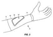
性質上、可撓性基板と、可撓性電子構成要素とから成る、可撓性電子ディスプレイ等の物品は、ユーザの腕、脚、胴体、または他の湾曲表面に動的に曲げ可能または共形化可能であって、種々の画像が、物品のユーザまたは装着者に容易に視認可能である様式において、可撓性電子ディスプレイ上に表示されることを可能にする。そのような可撓性電子ディスプレイを伴う動的可撓性取り付け可能な物品は、例えば、アームバンドの形態等、ユーザの身体に取り付けられる、またはその上に装着されてもよく、2つの次元において(例えば、縦方向および側方または横方向の両方に)曲がり、電子ディスプレイ(または他の可撓性電子構成要素)が位置する、種々の輪郭または身体表面に適合してもよい。そのような2次元曲がりは、ディスプレイが、より自然に感じる様式において、ユーザの皮膚に共形化し、それと重なり合うことを可能にする。動的可撓性取り付け可能な物品はまた、手の中または身体上に保持されていないとき、可撓性ディスプレイが視認されることを可能にする、コンピュータ、自動車のダッシュボード、オートバイのタンク等の複合湾曲表面(すなわち、1つを上回る方向に曲がりまたは湾曲するもの)を有する他のアイテムに容易に取り付けられる。なおもさらに、動的可撓性取り付け可能な物品は、平坦に配設されてもよく、電子ディスプレイがユーザに視認可能であることを可能にする様式において、表面上に配置される、またはそこに取り付けられてもよい。ある場合には、動的可撓性取り付け可能な物品は、デバイスのディスプレイが台を見ている人に可視となるようにもまた配向しながら、デバイスが充電されることを可能にする様式において、充電用接点を有する平坦な台上に載置されてもよい。 Articles, such as flexible electronic displays, consisting of a flexible substrate and flexible electronic components in nature, can be dynamically bent or co-formed onto a user's arm, leg, torso, or other curved surface. Shapeable and allows various images to be displayed on a flexible electronic display in a manner that is easily visible to a user or wearer of the article. A dynamically flexible attachable article with such a flexible electronic display may be attached to or worn on a user's body, for example, in the form of an armband, in two dimensions. It may bend (e.g., both longitudinally and laterally or laterally) to conform to various contours or body surfaces where the electronic display (or other flexible electronic component) is located. Such a two-dimensional bend allows the display to conform to and overlap the user's skin in a manner that feels more natural. The dynamically flexible attachable article also allows the flexible display to be viewed when not held in a hand or on the body, a computer, a car dashboard, a motorcycle tank, etc. Are easily attached to other items that have a composite curved surface (i.e., one that bends or curves in more than one direction). Still further, the dynamically flexible attachable article may be disposed flat or placed on or in a manner that allows the electronic display to be visible to a user. It may be attached to. In some cases, the dynamically flexible attachable article is in a manner that allows the device to be charged while the display of the device is also oriented to be visible to the person viewing the table. , May be mounted on a flat table having charging contacts.
いずれの場合も、取り付け可能な物品の電子ディスプレイまたは他の可撓性電子構成要素は、ユーザに視認可能であって、ユーザの片手もしくは両手に保持される必要なく、ユーザによって操作または作動されることが可能であって、ユーザが、ランニング、自転車の運転、ゴルフ、車の運転等の他の活動に従事またはそれを実施している間、電子デバイスを使用可能にする。 In each case, the electronic display or other flexible electronic component of the attachable article is visible to the user and operated or actuated by the user without having to be held in one or both hands of the user. The electronic device can be used while the user is engaged in or performing other activities, such as running, cycling, golfing, driving a car, and the like.
ある場合には、動的可撓性取付可能電子デバイスは、取付可能デバイスが、腕用スリーブ、脚用スリーブ、衣類、靴等の他の部材に除去可能に取り付けられることを可能にする支持体に取り付けられる、1つ、2つ、またはそれを上回る締結具もしくは留金部材を伴う、略長方形形状の形態における可撓性、例えば、曲げ可能な支持体上に配置される、可撓性電子ディスプレイを含む。デバイスの制御および通信電子機器は、例えば、可撓性基板内にあり得る、1つ以上の電子モジュール内に配置される。読みやすさのために、1つ以上の電子機器モジュールは、本明細書では、単数形(すなわち、「電子機器モジュール」)で言及されるが、動的可撓性取付可能電子デバイスは、1つを上回る電子機器モジュールを含んでもよいことを理解されたい。 In some cases, the dynamically flexible attachable electronic device includes a support that allows the attachable device to be removably attached to other members such as arm sleeves, leg sleeves, clothing, shoes, and the like. Flexible in the form of a generally rectangular shape, with one, two or more fasteners or clasps attached to the flexible electronics, eg, disposed on a bendable support Including display. The device control and communication electronics are located in one or more electronic modules, which may be, for example, in a flexible substrate. For readability, one or more electronics modules are referred to herein as singular (ie, "electronics modules"), but the dynamically flexible attachable electronic device is referred to as one or more. It should be understood that more than one electronics module may be included.
電子機器モジュールは、ディスプレイドライバと通信し、電子ディスプレイ(または他の可撓性電子構成要素)を駆動し、固定もしくは変更可能メッセージ、挿絵、写真等を表示する、光を放出する、感知を行う等のためのアプリケーションまたはプログラム等、アプリケーションもしくはプログラミングを実装するためのプロセッサを含む。電子モジュールはまた、種々の時間に電子ディスプレイ上に表示されるべきデータ、例えば、写真、画像、メッセージ、ビデオ等を記憶するため、かつ異なる時間に種々のディスプレイタスクを行うために、アプリケーションによって使用されるべき構成データ等のアプリケーションおよびアプリケーションデータを記憶するためのメモリを含む。性質上、堅くあり得る、電子機器モジュールはまた、電子ディスプレイ、プロセッサ、ディスプレイドライバ、および他の電子要素に給電するためのバッテリと、無線または有線様式のいずれかにおいて、バッテリを充電するためのバッテリ充電デバイスと、他のコンピュータデバイスが、プロセッサ、ディスプレイドライバ、およびメモリと通信し、電子ディスプレイ上に表示されるべき新しいまたは異なる画像もしくはメッセージを提供し、取付可能電子デバイスの電子ディスプレイの動作を構成すること等を可能にする、通信モジュールとを含んでもよい。 The electronics module communicates with a display driver, drives an electronic display (or other flexible electronic component), displays fixed or changeable messages, illustrations, pictures, etc., emits light, senses. Including a processor for implementing the application or programming, such as an application or program for the same. The electronic module is also used by the application to store data to be displayed on the electronic display at various times, such as photos, images, messages, videos, etc., and to perform various display tasks at different times. It includes an application such as configuration data to be performed and a memory for storing application data. The electronics module, which can be rigid in nature, also includes a battery for powering electronic displays, processors, display drivers, and other electronic components, and a battery for charging the battery in either a wireless or wired manner. The charging device and other computing devices communicate with the processor, display driver, and memory, provide new or different images or messages to be displayed on the electronic display, and configure operation of the electronic display of the attachable electronic device. And a communication module that enables the
可撓性電子構成要素は、種々の好適なプラスチックのいずれか等の任意の所望の可撓性電子ディスプレイ材料を使用して加工され得る、可撓性電子ディスプレイであってもよい。所望に応じて、可撓性電子ディスプレイは、同一または異なる可撓性材料から形成される別個の正面および背面基板上に配置される画素要素を有する、ディスプレイとして製造されてもよい。電子ペーパが可撓性ディスプレイとして使用される場合等のある場合には、材料の別個の層が、正面と背面材料との間に配置され、画素要素を形成してもよい。いずれの場合も、これらの基板材料は、ともに載置され、可撓性電子ディスプレイを形成してもよく、これは、次いで、皮製支持体、曲げ可能金属支持体、ゴム支持体等の可撓性支持体上に配置されてもよく、その組み合わせは、腕、脚、胴体等の装着者の身体の一部の形状に共形化する、または取り付け可能な物品が取り付けられ得る他のアイテムの形状に共形化する種々の様式において、撓曲または湾曲させられることができる。別の場合には、取付可能電子デバイスは、可撓性電子ディスプレイにわたって、またはその上部に配置され、ユーザが、可撓性電子ディスプレイに対してデータを入力する、または入力アクションを行うことを可能にする、可撓性の、例えば、透明のタッチスクリーンインターフェースを含んでもよい。所望に応じて、入力は、動的可撓性取付可能デバイス内に含まれる他のセンサによって検出される、ジェスチャまたは他の入力の形態であってもよく、センサによって検出されるジェスチャは、電子デバイスを、動作モードを変更させるように等、所定の様式において動作させてもよい。 The flexible electronic component can be a flexible electronic display that can be processed using any desired flexible electronic display material, such as any of a variety of suitable plastics. If desired, the flexible electronic display may be manufactured as a display having the pixel elements disposed on separate front and back substrates formed from the same or different flexible materials. In some cases, such as when ePaper is used as a flexible display, separate layers of material may be placed between the front and back materials to form pixel elements. In each case, these substrate materials may be mounted together to form a flexible electronic display, which in turn may be a flexible support such as a leather support, a bendable metal support, a rubber support, or the like. Other items that may be placed on a flexible support, the combination conforming to the shape of a part of the wearer's body, such as an arm, leg, torso, or to which an attachable article may be attached Can be flexed or curved in various ways to conform to the shape of In another case, the attachable electronic device is located across or on the flexible electronic display, allowing a user to enter data or perform input actions on the flexible electronic display. May include a flexible, eg, transparent, touch screen interface. If desired, the input may be in the form of a gesture or other input detected by other sensors contained within the dynamically flexible attachable device, and the gesture detected by the sensor may be an electronic gesture. The device may be operated in a predetermined manner, such as to change the mode of operation.
そのように形成される電子ディスプレイデバイスは、例えば、ユーザが、例えば、写真、ユーザまたは他者によって生成されるデジタル挿絵、ユーザに送信される、もしくはユーザによって生成されるメッセージ、リマインダ、教訓的、教育的、または啓発的メッセージを提供する文書、電子カード、広告、個人用覚書、個人用Outlook(R)カレンダ等のカレンダ等を含む、単一タイプまたは複数の異なるタイプのデジタル媒体を電子ディスプレイ上に同時に描写もしくは表示させることを可能にしてもよい。An electronic display device so formed may be used, for example, by a user, e.g., a photograph, a digital illustration generated by a user or others, a message sent to or generated by a user, a reminder, a lesson, Single or multiple different types of digital media, including documents, e-cards, advertisements, personal memorandums, personal Outlook(R) calendars, etc., that provide educational or enlightening messages on electronic displays At the same time.
より具体的には、ディスプレイドライバは、その上に、メモリ内に記憶された1つ以上の画像、メッセージ、デジタル挿絵、ビデオ等を表示することによって、電子ディスプレイを駆動させるように構成可能であってもよい。ある場合には、ディスプレイドライバは、電極またはコネクタのセットに接続され、順に、可撓性ディスプレイの画素要素に接続され、ディスプレイドライバは、個別のコンテンツを各電極またはコネクタに提供し、可撓性ディスプレイ上に表示される画像を生成する。ディスプレイドライバは、可撓性電子ディスプレイを介して、固定画像を表示してもよく、メモリにアクセスし、新しい画像をディスプレイに提供することによって等、可撓性電子ディスプレイ上に表示されている画像を時間毎に変更してもよく、リアルタイムビデオ等のビデオを表示してもよく、および/または他のタイプのデジタル媒体を表示してもよい。同様に、ディスプレイドライバは、取付可能電子デバイスの異なる時間または異なるモードにおいて、多くの異なるアプリケーションに関連付けられた種々のインターフェースを可撓性ディスプレイ上に提示させてもよい。例えば、ディスプレイドライバは、プロセッサ内で実行される種々の異なるアプリケーションによって駆動され、カレンダインターフェース、電子メールインボックスインターフェース、アラームクロックインターフェース、キーボードインターフェース、歩数計インターフェース等を表示してもよい。当然ながら、任意の他の特殊目的アプリケーションも、プロセッサ上に実装され、ディスプレイを駆動し、他のタイプのインターフェースをディスプレイ上に提供してもよい。これらのインターフェースは、可撓性ディスプレイ上の同一場所に位置し、異なる時間に表示されてもよく、可撓性ディスプレイ上の異なる場所に位置し、同一または異なる時間に表示されてもよい。 More specifically, the display driver can be configured to drive an electronic display by displaying one or more images, messages, digital illustrations, videos, etc. stored in memory thereon. You may. In some cases, the display driver is connected to a set of electrodes or connectors, which in turn are connected to the pixel elements of the flexible display, and the display driver provides individual content to each electrode or connector, Generate an image to be displayed on the display. The display driver may display the fixed image via the flexible electronic display, access the memory and provide a new image to the display, such as by displaying the image on the flexible electronic display. May change from time to time, may display video, such as real-time video, and / or may display other types of digital media. Similarly, the display driver may cause various interfaces associated with many different applications to be presented on the flexible display at different times or in different modes of the attachable electronic device. For example, the display driver may be driven by a variety of different applications running in the processor and display a calendar interface, an email inbox interface, an alarm clock interface, a keyboard interface, a pedometer interface, and the like. Of course, any other special purpose applications may also be implemented on the processor to drive the display and provide other types of interfaces on the display. These interfaces may be co-located on the flexible display and displayed at different times, or may be positioned differently on the flexible display and displayed at the same or different times.
なおもさらに、バッテリ充電ユニットが、バッテリに接続されてもよく、例えば、誘導結合式充電技法または直接結合式充電技法を使用して、バッテリを充電するように動作してもよい。バッテリ充電ユニットは、例えば、誘導結合式充電システムの一部であってもよく、外部充電ユニットによって生成される電磁波に応答し、取り付け可能な物品が外部充電ユニットの近傍に配置されると、バッテリを充電してもよい。別の場合には、バッテリ充電器は、デバイスの運動(取付可能電子デバイスがリストバンドの形態であるとき、腕の移動に関連付けられるもの等)を電気エネルギーに変換し、次いで、バッテリを充電するために使用される、運動エネルギー充電ユニットであってもよい。 Still further, a battery charging unit may be connected to the battery and may operate to charge the battery using, for example, an inductively coupled charging technique or a direct coupled charging technique. The battery charging unit may be, for example, part of an inductively coupled charging system, which responds to electromagnetic waves generated by the external charging unit, and when the attachable article is located near the external charging unit, the battery is charged. May be charged. In another case, the battery charger converts the movement of the device (such as that associated with arm movement when the attachable electronic device is in the form of a wristband) into electrical energy and then charges the battery Kinetic energy charging unit used for
なおもさらに、通信モジュールは、プロセッサ、ドライバ、メモリおよび/または可撓性電子ディスプレイが、例えば、Wi−Fiネットワーク、セルラーネットワーク、Bluetooth(登録商標)接続、近距離通信(NFC)接続、赤外線通信技法、無線周波数識別(RFID)デバイス、またはタグ等に関連付けられた無線通信を使用して、コンピュータ、携帯電話、タブレットデバイス、遠隔制御ユニット等の外部源またはデバイスと通信することを可能にしてもよい。通信モジュールは、ドライバが、メモリ内への記憶のための新しい画像または他のデジタル媒体を受信し、最終的に、可撓性電子ディスプレイ上に、種々の様式において電子ディスプレイの制御を行うためのプロセッサまたはドライバによる実行のための新しいアプリケーションと、ディスプレイドライバが、可撓性電子ディスプレイを制御し、画像および他の情報を表示するように動作する様式を構成するための新しい構成情報とを表示することを可能にするように動作してもよい。このように、ユーザは、例えば、無線通信ネットワークを介して、取り付け可能な物品を再プログラムし、異なる写真、画像、メッセージ等を異なる時間に表示し、異なるアプリケーションを異なる時間または異なる場所で実行してもよい。通信モジュールは、取付可能デバイスが、情報をデバイスのメモリに書き込むために、コンピュータに繋がれる、または別様に、そこに有線接続される必要性を排除するように動作する。 Still further, the communication module may include a processor, a driver, a memory, and / or a flexible electronic display, such as a Wi-Fi network, a cellular network, a Bluetooth® connection, a near field communication (NFC) connection, an infrared communication. Using techniques, radio frequency identification (RFID) devices, or wireless communications associated with tags and the like to enable communication with external sources or devices such as computers, cell phones, tablet devices, remote control units, etc. Good. The communication module is for the driver to receive new images or other digital media for storage in memory and ultimately to control the electronic display in various ways on the flexible electronic display. Displaying a new application for execution by the processor or driver and new configuration information to configure the manner in which the display driver controls the flexible electronic display and operates to display images and other information. It may operate to allow that. In this way, the user may reprogram the attachable item, display different photos, images, messages, etc. at different times, run different applications at different times or different locations, for example, via a wireless communication network. You may. The communication module operates to eliminate the need for the attachable device to be tied to, or otherwise wired to, a computer to write information to the memory of the device.
なおもさらに、メモリは、ユーザによって取付可能電子デバイスに提供またはダウンロードされた1つ以上のアプリケーションを記憶してもよく、プロセッサは、それを実行してもよい。これらのアプリケーションは、ユーザが、任意の所与の時間に表示するための特定のデジタル媒体または画像、画像が表示されるべき順序、画像が、背景色、境界、視覚的効果等の表示特徴を変更するであろう速度等、可撓性電子ディスプレイを伴う取付可能デバイスの動作特徴を指示またはプログラムすることを可能にしてもよい。さらに、アプリケーションは、例えば、Wi−Fi接続、セルラー接続、Bluetooth(登録商標)もしくはNFC接続、または任意の他の無線通信ネットワークもしくは接続を介して提供される、電子カード、広告または宣伝情報等、可撓性電子ディスプレイ上に表示され得る情報を取得するために、通信モジュールを介した通信を可能にする、またはそれを行ってもよい。 Still further, the memory may store one or more applications provided or downloaded by the user to the attachable electronic device, and the processor may execute it. These applications allow the user to display specific digital media or images for display at any given time, the order in which the images are to be displayed, and the images to display features such as background colors, borders, visual effects, etc. It may be possible to indicate or program operating characteristics of the attachable device with the flexible electronic display, such as the speed that will change. Further, the application may include, for example, an electronic card, advertising or promotional information provided via a Wi-Fi connection, a cellular connection, a Bluetooth® or NFC connection, or any other wireless communication network or connection. Communication via a communication module may be enabled or performed to obtain information that may be displayed on a flexible electronic display.
ある場合には、汎用マイクロプロセッサタイプのコントローラまたは特殊目的コントローラ、バッテリ、バッテリ充電ユニット、コンピュータ可読メモリ、および通信モジュールであり得る、プロセッサは、例えば、取り付け可能な物品の側壁または別個の堅いモジュール内に統合されてもよく、これらの構成要素は、デバイスの外部が暴露される、水、空気、泥等からシールまたは別様に保護されてもよい。これらの電子構成要素のいずれかまたは全ては、密閉シール様式において封入され、外力および環境上の危険へのこれらの構成要素のいかなる直接暴露も防止してもよい。 In some cases, the processor may be a general-purpose microprocessor-type or special purpose controller, battery, battery charging unit, computer readable memory, and communication module, for example, in the side wall of an attachable article or in a separate rigid module. These components may be sealed or otherwise protected from water, air, mud, etc., to which the exterior of the device is exposed. Any or all of these electronic components may be encapsulated in a hermetically sealed fashion to prevent any direct exposure of these components to external forces and environmental hazards.
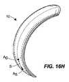
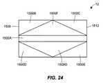
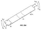
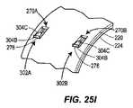
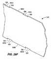
なおもさらに、取り付け可能な物品の可撓性支持体は、例えば、可撓性ディスプレイが受け得る、可能性として考えられる運動のタイプを制限することによって、可撓性ディスプレイを保護するための種々のタイプの構造を組み込んでもよい。これらのタイプの構造は、例えば、可撓性支持体内またはその上に配置される、1つ以上のセットの横方向および/または縦方向バー、支柱、または支索、堅いが、蝶着された材料のメッシュ等を含み、2つの次元における可撓性支持体の運動を制限し、それによって、2つの次元のそれぞれにおける可撓性ディスプレイの曲がりに起因する、可撓性ディスプレイへの損傷を防止することができる。同様に、1つ以上の縦方向および/または横方向部材が、可撓性支持体内に構成され、デバイスの縦軸および/またはデバイスの横軸の一方もしくは両方の周囲における可撓性支持体の曲げ運動を制限してもよい。本構造は、したがって、可撓性電子ディスプレイの種々の層を亀裂、座屈、剥離、または別様に損傷させ得る、曲げ運動からの可撓性ディスプレイへの損傷を防止するように、1つ以上の方向における可撓性ディスプレイの撓曲を防止または制限する。なおもさらに、可撓性支持体は、2つの次元における支持体(それによって、支持体上に搭載されるディスプレイ)の曲がりを制限するように動作する、材料の蝶着されたシートを含んでもよい。殆どの場合、可撓性基板は、2つの次元における可撓性基板の曲げ半径を、2つの次元のそれぞれにおける可撓性電子ディスプレイの曲がりの許容値内の範囲に制限するようにともに動作する、曲がりを制限する構造要素を含む。しかしながら、可撓性基板は、2つの次元のそれぞれにおける曲がりの異なる量または範囲を可能にしてもよい。所望に応じて、電子機器モジュールは、堅くあってもよく、例えば、可撓性基板の端部または可撓性基板の2つの端部間の任意の点において、可撓性基板に結合されてもよい。同様に、可撓性支持体は、可撓性ディスプレイの縁に沿って配置され、可撓性電子ディスプレイの縁または側面における衝突による可撓性電子ディスプレイへの損傷を防止または制限する、例えば、金属ワイヤまたは他の材料から形成される縁またはリッジを含んでもよい。 Still further, the flexible support of the attachable article may provide various means for protecting the flexible display, for example, by limiting the types of possible movements that the flexible display may undergo. May be incorporated. These types of structures may include, for example, one or more sets of lateral and / or longitudinal bars, struts, or braces, rigid but hinged, disposed within or on a flexible support. Including movement of the flexible support in two dimensions, including a mesh of material or the like, thereby preventing damage to the flexible display due to bending of the flexible display in each of the two dimensions can do. Similarly, one or more longitudinal and / or transverse members may be configured within the flexible support and the flexible support around one or both of the device longitudinal axis and / or the device transverse axis. The bending movement may be restricted. The present structure thus provides one way to prevent damage to the flexible display from bending motion, which can crack, buckle, peel, or otherwise damage various layers of the flexible electronic display. Prevent or limit flexing of the flexible display in the above directions. Still further, the flexible support may include a hinged sheet of material that operates to limit the bending of the support (and thereby the display mounted on the support) in two dimensions. Good. In most cases, the flexible substrates work together to limit the bending radius of the flexible substrate in the two dimensions to within a range of bending tolerances of the flexible electronic display in each of the two dimensions. , Including structural elements that limit bending. However, the flexible substrate may allow for different amounts or ranges of bend in each of the two dimensions. If desired, the electronics module may be rigid, for example, coupled to the flexible substrate at an end of the flexible substrate or at any point between the two ends of the flexible substrate. Is also good. Similarly, the flexible support is disposed along an edge of the flexible display to prevent or limit damage to the flexible electronic display due to a collision at the edge or side of the flexible electronic display, for example, It may include edges or ridges formed from metal wires or other materials.
別の実施形態では、取り付け可能な物品は、第1および第2の縦方向側と、第1ならびに第2の縦方向端部間に延在する第1および第2の横方向側とを有する、略長方形形状の基板を含み、可撓性基板は、可撓性基板の曲げ運動を各次元における特定の最小曲げ半径に制限するようにともに動作する、それぞれ、基板の第1および第2の横方向側と第1および第2の縦方向側との間に延在する、複数の相互接続された部品を有する。取り付け可能な物品はまた、可撓性基板上に配置される可撓性電子ディスプレイを含んでもよく、可撓性電子ディスプレイは、可撓性電子ディスプレイが、可撓性電子ディスプレイの電子機能性を損なうことなく曲げられ得る、最小臨界曲げ半径を有する。そのような最小臨界曲げ半径は、それを越えると、1回または少数回の曲がりに応じて、可撓性ディスプレイの電子機能性が損なわれる曲げ半径であり得る(例えば、1回、2回、3回等、最小臨界曲げ半径を越えて可撓性ディスプレイを曲げると、機能性が損なわれる)、またはそれを越えると、有意な回数の曲げ運動に応じて、可撓性ディスプレイの電子機能性の信頼性がなくなる、もしくは損なわれ得る、曲げ半径であり得る(例えば、最小臨界曲げ半径は、電子ディスプレイが、損なわれずに、有意な回数確実に曲げられ得る、最大最小半径であり得る)。なおもさらに、電子機器モジュールは、可撓性電子ディスプレイに電子的に接続され、可撓性電子ディスプレイに結合されるディスプレイドライバと、ディスプレイドライバに結合されるプロセッサとを含む。この場合、基板の縦方向における可撓性基板の特定の最小曲げ半径は、基板の横方向における可撓性電子ディスプレイの最小臨界曲げ半径を上回るまたはそれに等しくてもよい。さらに、これらの曲げ半径は、ディスプレイまたは他の可撓性電子構成要素が凹面および凸面となるように曲げられるとき、各方向に沿って異なってもよい(または同一であってもよい)。 In another embodiment, an attachable article has first and second longitudinal sides and first and second lateral sides extending between the first and second longitudinal ends. , Including a substantially rectangular shaped substrate, wherein the flexible substrate operates together to limit the bending motion of the flexible substrate to a particular minimum bending radius in each dimension, respectively. It has a plurality of interconnected components extending between a lateral side and first and second longitudinal sides. The attachable article may also include a flexible electronic display disposed on the flexible substrate, wherein the flexible electronic display increases the electronic functionality of the flexible electronic display. It has a minimum critical bending radius that can be bent without loss. Such a minimum critical bending radius may be a bending radius beyond which the electronic functionality of the flexible display is compromised, depending on one or a few bends (eg, once, twice, Bending the flexible display beyond the minimum critical bend radius, such as three times, would impair functionality), or beyond that, the electronic functionality of the flexible display in response to a significant number of bending movements Can be unreliable or compromised (e.g., the minimum critical bend radius can be a maximum minimum radius that an electronic display can be reliably bent a significant number of times without being compromised). Still further, the electronics module includes a display driver electronically coupled to the flexible electronic display and coupled to the flexible electronic display, and a processor coupled to the display driver. In this case, the specific minimum bending radius of the flexible substrate in the longitudinal direction of the substrate may be greater than or equal to the minimum critical bending radius of the flexible electronic display in the lateral direction of the substrate. Further, these bending radii may be different (or may be the same) along each direction when the display or other flexible electronic component is bent to be concave and convex.
所望に応じて、一実施形態では、可撓性基板は、ヒンジを用いて相互接続される材料の一連の堅い部品を含んでもよく、ヒンジは、可撓性基板上に配置されるとき、可撓性電子ディスプレイの曲がりを可撓性電子ディスプレイの曲がりの許容値内に制限する。材料の堅い部品は、基板に沿って、縦方向および横方向に配置されてもよく、ヒンジは、ヒンジの曲げ運動の範囲を制限するように相互作用する、突出部を含んでもよい。同様に、可撓性基板は、可撓性材料に沿って縦方向および横方向に離間される堅い要素を伴う、可撓性材料を含んでもよく、堅い要素は、バンドの縦方向におけるよりもバンドの横方向における可撓性基板の曲がりを制限するように動作する、またはその逆であってもよい。なおもさらなる実施形態では、可撓性基板は、可撓性電子ディスプレイに最も近接して配置されている第1の不断区分を有し、かつ第1の区分に隣接して配置され、その中に配置される溝を有する、第2の区分を有する、柔軟性材料を含んでもよく、溝は、可撓性基板の片側から可撓性基板の他側に延在する。所望に応じて、第2の区分はさらに、その中に配置される1つ以上の縦方向溝を含んでもよく、縦方向溝は、少なくとも部分的に、可撓性基板の一方の縦方向端部から可撓性基板の他方の縦方向端部に延在する。加えて、可撓性基板は、互に隣接して縦方向または横方向に配置される2つの部分を有してもよく、第1の部分は、第2の部分が曲げられ得る最小曲率半径と異なる、最小曲率半径に曲げられることができる。また、可撓性基板は、基板に沿って互いに対して縦方向または横方向に配置される、複数の区分を有してもよく、各区分は、複数の最小曲率半径の1つに曲げられることができ、区分の少なくとも2つは、他の区分の1つの最小曲率半径未満である、最小曲率半径に曲げられることができる。なおもさらなる場合には、可撓性基板は、可撓性電子ディスプレイの各横方向および/または縦方向側(すなわち、横方向における縁に配置される側、または縦方向端部間に縦方向に延在する側)において、可撓性電子ディスプレイの上方に延在する、縁部品を有してもよく、縁部品は、軟質柔軟性材料の内側に配置される材料の第1の曲げ可能部品を含んでもよい。この場合、材料の第1の曲げ可能部品は、軟質柔軟性材料より硬質であってもよい。 If desired, in one embodiment, the flexible substrate may include a series of rigid components of a material that are interconnected using hinges, which, when placed on the flexible substrate, can be flexible. Limit the flexing of the flexible electronic display to within the flexing tolerance of the flexible electronic display. Rigid parts of material may be arranged longitudinally and laterally along the substrate, and the hinge may include protrusions that interact to limit the range of bending movement of the hinge. Similarly, the flexible substrate may include a flexible material, with rigid elements spaced longitudinally and laterally along the flexible material, wherein the rigid elements are more rigid than in the longitudinal direction of the band. It may operate to limit the bending of the flexible substrate in the lateral direction of the band, or vice versa. In a still further embodiment, the flexible substrate has a first perforated section located closest to the flexible electronic display and is located adjacent to the first section, wherein: May include a flexible material having a second section having a groove disposed therein, wherein the groove extends from one side of the flexible substrate to the other side of the flexible substrate. If desired, the second section may further include one or more longitudinal grooves disposed therein, wherein the longitudinal grooves are at least partially at one longitudinal end of the flexible substrate. Extending from the portion to the other longitudinal end of the flexible substrate. In addition, the flexible substrate may have two portions arranged longitudinally or laterally adjacent to each other, the first portion being the minimum radius of curvature over which the second portion can be bent And can be bent to a minimum radius of curvature. Also, the flexible substrate may have a plurality of sections disposed longitudinally or laterally with respect to each other along the substrate, each section being bent to one of a plurality of minimum radii of curvature. And at least two of the sections can be bent to a minimum radius of curvature that is less than a minimum radius of curvature of one of the other sections. In still a further case, the flexible substrate is longitudinally between each lateral and / or longitudinal side of the flexible electronic display (ie, the side located at the edge in the lateral direction, or between the longitudinal ends). On the side that extends to the upper side of the flexible electronic display, the edge part may be a first bendable material of a material disposed inside the soft flexible material. Parts may be included. In this case, the first bendable part of the material may be harder than the soft flexible material.
なおもさらに、可撓性電子ディスプレイは、リード線が可撓性ディスプレイのディスプレイ面積を励起するために使用される、可撓性ディスプレイの縁が、ディスプレイの下方または下側に曲げられもしくは折畳されるように形成されることによって、取り付け可能な物品の上側表面上に最大使用可能ディスプレイ面積を提示するように構成されてもよい。そのような構成は、ディスプレイ画素が位置しない、取り付け可能な物品の上側または外側表面上に面積を有する必要性を制限もしくは低減させる。
本発明は、例えば、以下を提供する。
(項目1)
物品であって、
第1の次元に沿って、かつ前記第1の次元と異なる第2の次元に沿って曲がるために構成されている可撓性電子構成要素と、
前記可撓性電子構成要素に結合されている可撓性支持体であって、前記可撓性支持体は、前記第1および第2の次元に沿った前記可撓性電子構成要素の曲がりを前記可撓性電子構成要素の曲がりの許容値内の範囲に制限するように構成されている曲がりを制限する構造を含む、可撓性支持体と、
を備えている、物品。
(項目2)
前記可撓性電子構成要素は、前記可撓性電子構成要素を損なうことなく、前記可撓性電子構成要素が前記第1の次元に沿って曲げられることが可能な第1の最小臨界曲げ半径と、前記可撓性電子構成要素を損なうことなく、前記可撓性電子構成要素が前記第2の次元に沿って曲げられることが可能な第2の最小臨界曲げ半径とを有し、前記可撓性電子構成要素の曲がりの許容値は、少なくとも部分的に、前記第1および第2の最小臨界曲げ半径によって画定されている、項目1に記載の物品。
(項目3)
前記第2の最小臨界曲げ半径は、前記第1の最小臨界曲げ半径と異なる、項目2に記載の物品。
(項目4)
前記曲がりを制限する構造は、前記第1の次元に沿った前記可撓性電子構成要素の曲がりを前記可撓性電子構成要素の前記第1の最小臨界曲げ半径より大きいかまたはそれに等しい第1の曲げ半径に制限し、前記第2の次元に沿った前記可撓性電子構成要素の曲がりを前記可撓性電子構成要素の前記第2の最小臨界曲げ半径より大きいかまたはそれに等しい第2の曲げ半径に制限するように構成されている、項目1〜3のいずれか1項に記載の物品。
(項目5)
前記第2の曲げ半径は、前記第1の曲げ半径と異なる、項目4に記載の物品。
(項目6)
前記可撓性電子構成要素は、可撓性ディスプレイ、可撓性電子回路、可撓性シート、センサタグ、または可撓性OLED照明を備えている、項目1〜5のいずれか1項に記載の物品。
(項目7)
前記第1の次元は、縦方向次元を備え、前記第2の次元は、横方向次元を備えている、項目1〜6のいずれか1項に記載の物品。
(項目8)
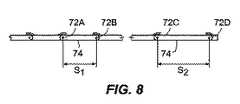
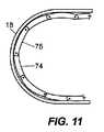
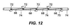
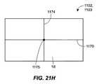
前記曲がりを制限する構造は、前記可撓性支持体の上部または底部側に形成されている第1の複数の溝および第2の複数の溝を備え、前記第1の複数の溝は、前記可撓性支持体の一方の横方向側から前記可撓性支持体の他方の横方向側に延び、前記第1の次元における前記可撓性電子構成要素の曲がりを制限するように構成され、前記第2の複数の溝は、前記可撓性支持体の一方の縦方向側から前記可撓性支持体の他方の縦方向側に延び、前記第2の次元における前記可撓性電子構成要素の曲がりを制限するように構成されている、項目1〜7のいずれか1項に記載の物品。
(項目9)
前記第2の複数の溝は、前記第1の複数の溝に直交している、項目8に記載の物品。
(項目10)
前記可撓性支持体は、前記可撓性電子構成要素に最も近接して配置されている第1の不断区分を有し、かつ前記第1の区分に隣接して配置されている第2の区分を有する柔軟性材料を含み、前記第2の区分は、その中に形成されている第1および第2の複数の溝を有し、前記第1および第2の複数の溝の各溝は、その溝に隣接する前記可撓性支持体の部分間の局所曲がりを制限するように構成されている、項目8または9に記載の物品。
(項目11)
前記第1および第2の複数の溝の側面は、前記可撓性電子構成要素が前記可撓性電子構成要素の曲がりの許容値内の範囲の外に曲げられるのに先立って、前記可撓性支持体の曲がりに応じて、特定の溝の側面が触れ合うように、テーパ状である、項目8〜10のいずれか1項に記載の物品。
(項目12)
前記第1の複数の溝は、前記可撓性支持体を横断して均一に離間されている、項目8〜11のいずれか1項に記載の物品。
(項目13)
前記第1の複数の溝は、前記可撓性支持体を横断して異なる距離で離間されている、項目8〜11のいずれか1項に記載の物品。
(項目14)
前記第2の複数の溝は、前記可撓性支持体を横断して均一に離間されている、項目8〜13のいずれか1項に記載の物品。
(項目15)
前記第2の複数の溝は、前記可撓性支持体を横断して異なる距離で離間されている、項目8〜13のいずれか1項に記載の物品。
(項目16)
前記曲がりを制限する構造は、各々が前記可撓性支持体の上部または底部側に形成されている第1の複数の溝と、第2の複数の溝と、第3の複数の溝とを備え、前記第1、第2、および第3の複数の溝は、互いに対してある角度で形成されている、項目1〜8のいずれか1項に記載の物品。
(項目17)
前記第1、第2、および第3の複数の溝は、互いに対して約60度の角度で形成されている、項目16に記載の物品。
(項目18)
前記可撓性支持体は、前記可撓性電子構成要素に移動可能に結合されており、前記可撓性支持体および前記可撓性電子構成要素は、取り付け可能な物品が、前記第1の次元に沿って、および/または前記第2の次元に沿って曲げられるとき、互いに対して移動可能であることによって、前記物品は、前記可撓性電子構成要素自体の曲がりの範囲に実質的に類似する曲がりの範囲を有することが可能である、項目1〜17のいずれか1項に記載の物品。
(項目19)
前記可撓性支持体および前記可撓性電子構成要素は、互いに対して縦方向に移動可能である、項目18に記載の物品。
(項目20)
前記可撓性支持体は、前記可撓性電子構成要素にスライド可能に結合されている、項目18または19に記載の物品。
(項目21)
前記可撓性支持体は、第1の長さおよび第1の幅を有し、前記可撓性電子構成要素は、第2の長さおよび第2の幅を有し、前記第2の長さは、前記第1の長さより短く、前記第2の幅は、前記第1の幅より小さい、項目18〜20のいずれか1項に記載の物品。
(項目22)
前記可撓性支持体は、空洞を画定し、前記可撓性電子構成要素は、前記空洞内に配置されている、項目18〜21のいずれか1項に記載の物品。
(項目23)
前記可撓性支持体は、底壁と、前記底壁から上向きに延びている一対の対向する側壁とによって画定され、前記空洞は、前記底壁と前記対の対向する側壁との間に画定されている、項目22に記載の物品。
(項目24)
前記側壁は、前記可撓性電子構成要素を包囲している、項目23に記載の物品。
(項目25)
前記可撓性支持体は、前記対向する側壁の各々に結合され、前記対向する側壁の各々から内向きに延びている保持部分をさらに含み、前記保持部分は、前記可撓性電子構成要素を前記可撓性支持体の空洞内に保持し、前記物品が、前記第1の次元および/または前記第2の次元に沿って曲げられるとき、前記曲がりを制限する構造としての役割を果たすように構成されている、項目23または24に記載の物品。
(項目26)
それぞれ、前記可撓性電子構成要素の第1および第2の部分に張力を加えるように構成されている第1および第2のばね要素をさらに備えている、項目18〜25のいずれか1項に記載の物品。
(項目27)
前記第1のばね要素は、前記可撓性支持体の一端に固定して取り付けられている第1の端部と、前記可撓性電子構成要素の対応する端に固定して取り付けられている第2の端部とを有し、前記第2のばね要素は、前記可撓性支持体の片側に固定して取り付けられている第1の端部と、前記可撓性電子構成要素の対応する側に固定して取り付けられている第2の端部とを有する、項目26に記載の物品。
(項目28)
前記可撓性電子構成要素の一部に張力を加えるように構成されているばね要素をさらに備えている、項目18〜25のいずれか1項に記載の物品。
(項目29)
前記ばね要素は、前記可撓性支持体の一端に固定して取り付けられている第1の端部と、前記可撓性電子構成要素の対応する端に固定して取り付けられている第2の端部とを有する、項目28に記載の物品。
(項目30)
前記可撓性支持体に結合され、少なくとも部分的に前記空洞を覆う可撓性シートをさらに備え、前記可撓性電子構成要素は、少なくとも部分的に、前記可撓性シートを通して可視であり、前記可撓性シートは、前記物品が、前記第1の次元および/または前記第2の次元に沿って曲げられているとき、前記可撓性電子構成要素を前記可撓性支持体の空洞内に保持するように構成されている、項目18〜24のいずれか1項に記載の物品。
(項目31)
前記可撓性シートは、前記対向する側壁の各々の上部部分に接着している、項目30に記載の物品。
(項目32)
前記可撓性支持体は、第1の材料から作製され、前記物品は、第2の材料から作製されている第2の可撓性支持体をさらに備え、前記第2の材料は、前記第1の可撓性材料より可撓性である、項目18〜21のいずれか1項に記載の物品。
(項目33)
前記第2の材料は、前記第1の材料より低いヤング率を有する、項目32に記載の物品。
(項目34)
前記第2の可撓性支持体は、空洞およびスロットを画定し、前記可撓性電子構成要素は、前記空洞内に配置され、前記第1の可撓性支持体は、前記スロット内に配置されている、項目32または33に記載の物品。
(項目35)
前記スロットは、前記第2の可撓性支持体が前記空洞内に配置されている前記可撓性電子構成要素に支持を提供可能であるように、前記空洞に近接して形成されている、項目34に記載の物品。
(項目36)
前記可撓性電子構成要素は、前記空洞内で前記第2の可撓性支持体に接着している、項目34または35に記載の物品。
(項目37)
前記第1の可撓性支持体および前記可撓性電子構成要素は、互いに対して縦方向に移動可能である、項目32〜36のいずれか1項に記載の物品。
(項目38)
前記曲がりを制限する構造は、前記可撓性支持体に沿って配置されている第1の複数のバーおよび第2の複数のバーを備えている、項目1〜37のいずれか1項に記載の物品。
(項目39)
前記第1の複数のバーは、前記可撓性支持体の一方の横方向側と前記可撓性支持体の他方の横方向側との間に延び、前記第2の複数のバーは、前記可撓性支持体の一方の縦方向側と前記可撓性支持体の他方の縦方向側との間に延びている、項目38に記載の物品。
(項目40)
前記可撓性支持体は、第1の材料から作製され、前記第1の複数のバーおよび前記第2の複数のバーは、前記第1の材料より堅い第2の材料から作製されている、項目38または39に記載の物品。
(項目41)
前記曲がりを制限する構造は、前記可撓性支持体に沿って配置されている第3の複数のバーをさらに備え、前記第1、第2、および第3の複数のバーは、互いに対してある角度で配置されている、項目38に記載の物品。
(項目42)
前記第1、第2、および第3の複数のバーは、互いに対して約60度の角度で配置されている、項目41に記載の物品。
(項目43)
前記曲がりを制限する構造は、複数の相互接続されたリンクを備えている、項目1〜7のいずれか1項に記載の物品。
(項目44)
前記曲がりを制限する構造は、ヒンジを用いて相互接続された材料の複数の堅い部品を含み、前記ヒンジは、前記可撓性電子ディスプレイの曲がりを前記可撓性電子構成要素の曲がりの許容値内に制限するように構成されている、項目43に記載の物品。
(項目45)
前記複数の堅い部品は、前記可撓性支持体に沿って横方向に配置されている材料の第1の一連の堅い部品と、前記可撓性支持体に沿って縦方向に配置されている材料の第2の一連の堅い部品とを含む、項目44に記載の物品。
(項目46)
前記曲がりを制限する構造は、前記材料の第1の一連の堅い部品の曲がりを制限するように構成されている第1の一連の突出部と、前記材料の第2の一連の堅い部品の曲がりを制限するように構成されている第2の一連の突出部とを含む、項目45に記載の物品。
(項目47)
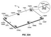
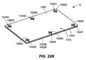
前記可撓性電子構成要素は、実質的に平坦な位置に置かれた場合、基準平面内に2次元エリアを画定し、前記可撓性支持体の曲がりを制限する構造は、前記可撓性電子構成要素が前記第1の次元における第1の曲がりの軸および前記第2の次元における第2の曲がりの軸に沿って同時に曲げられた場合、前記基準平面上への前記第1の曲がりの軸の第1の投影と前記基準平面上への前記第2の曲がりの軸の第2の投影とが前記基準平面の前記2次元エリア内に位置する点において交差しないように、前記可撓性電子構成要素の曲がりを制約するように構成されている、項目1〜7のいずれか1項に記載の物品。
(項目48)
前記曲がりを制限する構造は、第1の基板と、前記第1の基板に移動可能に結合されている第2の基板と、前記第1の基板内に形成されている複数の開口と、前記第2の基板に結合されている複数の突出部とを備え、前記複数の突出部は、それぞれ、前記複数の開口内に移動可能に配置されている、項目47に記載の物品。
(項目49)
前記複数の開口の各々は、前記可撓性電子構成要素の曲がりを制約するように配置されている内壁によって画定されている、項目48に記載の物品。
(項目50)
前記可撓性支持体は、第1の基板と、前記第1の基板に移動可能に結合されている第2の基板と、前記第1の基板内に形成されている複数のスロットと、前記第2の基板に結合されている複数の突出部とを備え、前記複数の突出部は、それぞれ、前記複数のスロット内に移動可能に配置されている、項目47に記載の物品。
(項目51)
前記複数の突出部は、複数のピンを備えている、項目50に記載の物品。
(項目52)
前記スロットの各々は、前記可撓性電子構成要素の曲がりを制約するように配置されている複数の停止表面を画定している、項目50または51に記載の物品。
(項目53)
各スロットは、2つの縦方向に延びている部分と、前記縦方向に延びている部分に垂直の2つの横方向に延びている部分とによって画定されている、項目52に記載の物品。
(項目54)
各スロットは、4つの角度付けられた部分によってさらに画定され、各角度付けられた部分は、前記縦方向に延びている部分のうちの1つと前記横方向に延びている部分のうちの1つとの間に配置されている、項目53に記載の物品。
(項目55)
前記スロットのうちの1つ以上のものは、4つの停止表面を画定し、前記4つの停止表面は、横方向における前記可撓性電子構成要素の曲がりを制約するように配置されている第1および第2の停止表面と、縦方向における前記可撓性電子構成要素の曲がりを制約するように配置されている第3および第4の停止表面とを含む、項目52〜54のいずれか1項に記載の物品。
(項目56)
前記スロットのうちの1つ以上のものは、前記可撓性電子構成要素の曲がりを制約するように配置されている8つの停止表面を画定している、項目54または55に記載の物品。
(項目57)
前記第1の基板の一部は、固定点において、前記第2の基板の一部に局所的に固定して取り付けられている、項目48〜54のいずれか1項に記載の物品。
(項目58)
前記固定点は、前記可撓性支持体の中心部分に位置している、項目57に記載の物品。
(項目59)
前記固定点は、前記可撓性支持体の縦方向端部に隣接して位置している、項目57に記載の物品。
(項目60)
前記可撓性支持体は、複数の画定された曲がり領域を備えている、項目47〜49のいずれか1項に記載の物品。
(項目61)
前記可撓性支持体は、前記画定された曲がり領域の2つ以上のものの間に配置されている少なくとも1つの堅いゾーンを備えている、項目60に記載の物品。
(項目62)
前記画定された曲がり領域は、互いに対して角度付けられる、項目60または61に記載の物品。
(項目63)
物品であって、
第1の曲がりの軸および前記第1の曲がりの軸と異なる第2の曲がりの軸に沿って曲がるために構成されている可撓性電子構成要素と、
第1の基板と、
前記第1の基板に移動可能に結合されている第2の基板と、
前記第1の基板内に形成されている複数のスロットと、
前記第2の基板に結合され、前記複数のスロットの対応する1つ内に移動可能に配置されている複数の突出部と
を備え、
前記複数のスロットは、ある曲がりの範囲内における前記第1の曲がりの軸および前記第2の曲がりの軸に沿った前記可撓性電子構成要素の同時の曲がりを可能にするように画定されている、物品。
(項目64)
前記可撓性電子構成要素は、実質的に平坦な位置に置かれた場合、基準平面内に2次元エリアを画定し、前記複数のスロットは、前記可撓性電子構成要素が、前記第1の曲がりの軸に沿って、かつ前記第2の曲がりの軸に沿って同時に曲げられた場合、前記基準平面上への前記第1の曲がりの軸の第1の投影が、前記基準平面の前記2次元エリア内に位置する点において、前記基準平面上への前記第2の曲がりの軸の第2の投影と交差しないように画定されている、項目63に記載の物品。
(項目65)
前記第1および第2の曲がりの軸は、互に平行であるが同一平面上にはない、項目63または64に記載の物品。
(項目66)
前記第1および第2の曲がりの軸は、互に平行ではない、項目63または64に記載の物品。
(項目67)
前記第1の基板は、実質的に平坦な位置に置かれた場合、第1の平面内にある平面表面を画定し、前記第2の基板は、実質的に平坦な位置に置かれた場合、第2の平面内にある平面表面を画定し、前記第2の平面は、前記第1の平面に平行である、項目63〜66のいずれか1項に記載の物品。
(項目68)
前記可撓性電子構成要素は、可撓性ディスプレイ、可撓性電子回路、可撓性シート、センサタグ、または可撓性OLED照明を備えている、項目63〜67のいずれか1項に記載の物品。
(項目69)
前記複数の突出部は、複数のピンを備えている、項目63〜68のいずれか1項に記載の物品。
(項目70)
前記スロットの各々は、前記可撓性電子構成要素の曲がりを制約するように配置されている複数の停止表面を画定している、項目63〜69のいずれか1項に記載の物品。
(項目71)
各スロットは、2つ以上の部分によって画定され、各部分は、異なる方向に延びている、項目63〜70のいずれか1項に記載の物品。
(項目72)
前記スロットのうちの1つ以上のものは、偶数個の部分によって画定されている、項目71に記載の物品。
(項目73)
前記スロットのうちの1つ以上のものは、奇数個の部分によって画定されている、項目71または72に記載の物品。
(項目74)
各スロットの2つ以上の部分は、中心点から外向きに延びている、項目70〜73のいずれか1項に記載の物品。
(項目75)
前記スロットのうちの1つ以上のものの2つ以上の部分は、前記それぞれのスロットの中心点の周囲に対称的に配置されている、項目74に記載の物品。
(項目76)
前記スロットのうちの1つ以上のものの2つ以上の部分は、前記それぞれのスロットの中心点の周囲に非対称的に配置されている、項目74に記載の物品。
(項目77)
前記スロットのうちの1つ以上のものの2つ以上の部分は、異なる形状および/またはサイズを有する、項目71〜76のいずれか1項に記載の物品。
(項目78)
前記スロットのうちの1つ以上のものは、十字形状を有する、項目71〜77のいずれか1項に記載の物品。
(項目79)
各スロットは、2つの縦方向に延びている部分と、前記縦方向に延びている部分に垂直の2つの横方向に延びている部分とによって画定されている、項目63〜69、74、75、および78のいずれか1項に記載の物品。
(項目80)
各スロットは、4つの角度付けられた部分によってさらに画定され、各角度付けられた部分は、前記縦方向に延びている部分のうちの1つと前記横方向に延びている部分のうちの1つとの間に配置されている、項目79に記載の物品。
(項目81)
前記スロットのうちの1つ以上のものは、4つの停止表面を画定し、前記4つの停止表面は、横方向における前記可撓性電子構成要素の曲がりを制約するように配置されている第1および第2の停止表面と、縦方向における前記可撓性電子構成要素の曲がりを制約するように配置されている第3および第4の停止表面とを含む、項目63〜80のいずれか1項に記載の物品。
(項目82)
前記スロットのうちの1つ以上のものは、前記可撓性電子構成要素の曲がりを制約するように配置されている8つの停止表面を画定している、項目81に記載の物品。
(項目83)
前記第1の基板の一部は、固定点において、前記第2の基板の一部に局所的に固定して取り付けられている、項目63〜82のいずれか1項に記載の物品。
(項目84)
前記固定点は、前記支持構造の中心部分に位置している、項目83に記載の物品。
(項目85)
前記固定点は、前記支持構造の縦方向端部に隣接して位置している、項目84に記載の物品。
(項目86)
各スロットは、実質的に円形形状を有する、項目63〜69のいずれか1項に記載の物品。
(項目87)
物品であって、
第1の次元に沿って、かつ前記第1の次元と異なる第2の次元に沿って曲がるために構成されている可撓性電子構成要素と、
前記可撓性電子構成要素に移動可能に結合されている可撓性支持体と
を備え、
前記可撓性支持体と前記可撓性電子構成要素とは、取り付け可能な物品が前記第1の次元に沿って、および/または前記第2の次元に沿って曲げられたとき、前記物品が前記可撓性電子構成要素自体の曲がりの範囲に実質的に類似する曲がりの範囲を有し得るように、互いに対して移動可能である、物品。
(項目88)
前記可撓性支持体および前記可撓性電子構成要素は、互いに対して縦方向に移動可能である、項目87に記載の物品。
(項目89)
前記可撓性支持体は、前記可撓性電子構成要素にスライド可能に結合されている、項目87または88に記載の物品。
(項目90)
前記可撓性支持体は、第1の長さおよび第1の幅を有し、前記可撓性電子構成要素は、第2の長さおよび第2の幅を有し、前記第2の長さは、前記第1の長さより短く、前記第2の幅は、前記第1の幅より小さい、項目87〜89のいずれか1項に記載の物品。
(項目91)
前記可撓性支持体は、空洞を画定し、前記可撓性電子構成要素は、前記空洞内に配置されている、項目87〜90のいずれか1項に記載の物品。
(項目92)
前記可撓性支持体は、底壁と、前記底壁から上向きに延びている一対の対向する側壁とによって画定され、前記空洞は、前記底壁と前記対の対向する側壁との間に画定されている、項目91に記載の物品。
(項目93)
前記側壁は、前記可撓性電子構成要素を包囲している、項目92に記載の物品。
(項目94)
前記可撓性支持体は、前記対向する側壁の各々に結合され、前記対向する側壁の各々から内向きに延びている保持部分をさらに含み、前記保持部分は、前記可撓性電子構成要素を前記可撓性支持体の空洞内に保持するように構成されている、項目92または93に記載の物品。
(項目95)
前記可撓性電子構成要素の一部に張力を加えるように構成されているばね要素をさらに備えている、項目87〜93のいずれか1項に記載の物品。
(項目96)
前記ばね要素は、前記可撓性支持体の一端に固定して取り付けられている第1の端部と、前記可撓性電子構成要素の対応する端に固定して取り付けられている第2の端部とを有する、項目95に記載の物品。
(項目97)
それぞれ、前記可撓性電子構成要素の第1および第2の部分に張力を加えるように構成されている第1および第2のばね要素をさらに備えている、項目87〜94のいずれか1項に記載の物品。
(項目98)
前記第1のばね要素は、前記可撓性支持体の一端に固定して取り付けられている第1の端部と、前記可撓性電子構成要素の対応する端に固定して取り付けられている第2の端部とを有し、前記第2のばね要素は、前記可撓性支持体の片側に固定して取り付けられている第1の端部と、前記可撓性電子構成要素の対応する側に固定して取り付けられている第2の端部とを有する、項目95に記載の物品。
(項目99)
前記可撓性支持体に結合され、少なくとも部分的に前記空洞を覆う可撓性シートをさらに備え、前記可撓性電子構成要素は、少なくとも部分的に、前記可撓性シートを通して可視であり、前記可撓性シートは、前記物品が前記第1の次元および/または前記第2の次元に沿って曲げられているとき、前記可撓性電子構成要素を前記可撓性支持体の空洞内に保持するように構成されている、項目87〜93のいずれか1項に記載の物品。
(項目100)
前記可撓性シートは、前記対向する側壁の各々の上部部分に接着している、項目99に記載の物品。
(項目101)
前記可撓性支持体は、第1の材料から作製され、前記物品は、第2の材料から作製されている第2の可撓性支持体をさらに備え、前記第2の材料は、前記第1の可撓性材料より可撓性である、項目93〜98のいずれか1項に記載の物品。
(項目102)
前記第2の材料は、前記第1の材料より低いヤング率を有する、項目101に記載の物品。
(項目103)
前記第2の可撓性支持体は、空洞およびスロットを画定し、前記可撓性電子構成要素は、前記空洞内に配置され、前記第1の可撓性支持体は、前記スロット内に配置されている、項目101または102に記載の物品。
(項目104)
前記スロットは、前記第2の可撓性支持体が前記空洞内に配置されている前記可撓性電子構成要素に支持を提供可能であるように、前記空洞に近接して形成されている、項目103に記載の物品。
(項目105)
前記可撓性電子構成要素は、前記空洞内で前記第2の可撓性支持体に接着している、項目103または104に記載の物品。
(項目106)
前記第1の可撓性支持体および前記可撓性電子構成要素は、互いに対して縦方向に移動可能である、項目101〜105のいずれか1項に記載の物品。
(項目107)
項目1〜106のいずれか1つ以上の他の項目と組み合わせられる項目1〜106のいずれか1項。 Still further, the flexible electronic display may be such that the edges of the flexible display are bent or folded below or below the display, wherein the leads are used to excite the display area of the flexible display. May be configured to present a maximum usable display area on the upper surface of the attachable article. Such an arrangement limits or reduces the need to have an area on the upper or outer surface of the attachable article where the display pixels are not located.
The present invention provides, for example, the following.
(Item 1)
An article,
A flexible electronic component configured to bend along a first dimension and along a second dimension different from said first dimension;
A flexible support coupled to the flexible electronic component, the flexible support configured to bend the flexible electronic component along the first and second dimensions. A flexible support comprising a bend limiting structure configured to limit the range of bends of the flexible electronic component to within a range of bends;
An article comprising:
(Item 2)
The flexible electronic component has a first minimum critical bending radius at which the flexible electronic component can be bent along the first dimension without damaging the flexible electronic component. And a second minimum critical bending radius at which the flexible electronic component can be bent along the second dimension without damaging the flexible electronic component. The article of
(Item 3)
3. The article of
(Item 4)
The bend limiting structure may include a bend of the flexible electronic component along the first dimension that is greater than or equal to the first minimum critical bending radius of the flexible electronic component. And wherein the bending of the flexible electronic component along the second dimension is greater than or equal to the second minimum critical bending radius of the flexible electronic component. 4. The article of any of the preceding items, wherein the article is configured to limit to a bending radius.
(Item 5)
5. The article according to item 4, wherein the second bending radius is different from the first bending radius.
(Item 6)
Item 6. The flexible electronic component according to any one of
(Item 7)
7. The article of any one of the preceding items, wherein the first dimension comprises a vertical dimension and the second dimension comprises a lateral dimension.
(Item 8)
The structure for limiting the bending includes a first plurality of grooves and a second plurality of grooves formed on a top or bottom side of the flexible support, and the first plurality of grooves are Extending from one lateral side of the flexible support to the other lateral side of the flexible support, configured to limit bending of the flexible electronic component in the first dimension; The second plurality of grooves extend from one longitudinal side of the flexible support to the other longitudinal side of the flexible support, and the flexible electronic component in the second dimension. 8. The article according to any one of
(Item 9)
The article of
(Item 10)
The flexible support has a first permanent section located closest to the flexible electronic component and a second permanent section located adjacent to the first section. A flexible material having sections, wherein the second section has first and second plurality of grooves formed therein, wherein each of the first and second plurality of grooves is 10. The article of
(Item 11)
The sides of the first and second plurality of grooves may be configured such that the flexible electronic component is bent prior to being bent out of a range of bending tolerances of the flexible electronic component. The article according to any one of
(Item 12)
12. The article of any one of
(Item 13)
12. The article of any one of
(Item 14)
14. The article of any one of
(Item 15)
14. The article of any one of
(Item 16)
The structure for limiting the bending includes a first plurality of grooves, a second plurality of grooves, and a third plurality of grooves, each of which is formed on an upper or bottom side of the flexible support. 9. The article of any one of the preceding claims, wherein the first, second and third plurality of grooves are formed at an angle with respect to each other.
(Item 17)
The article of
(Item 18)
The flexible support is movably coupled to the flexible electronic component, and the flexible support and the flexible electronic component are attached to the first electronic component. By being movable with respect to each other when bent along a dimension and / or along the second dimension, the article is substantially in the range of bending of the flexible electronic component itself.
(Item 19)
(Item 20)
(Item 21)
The flexible support has a first length and a first width; the flexible electronic component has a second length and a second width; 21. The article of any one of
(Item 22)
22. An article according to any of
(Item 23)
The flexible support is defined by a bottom wall and a pair of opposing side walls extending upwardly from the bottom wall, and the cavity is defined between the bottom wall and the pair of opposing side walls. 23. The article according to
(Item 24)
The article of claim 23, wherein the sidewall surrounds the flexible electronic component.
(Item 25)
The flexible support further includes a holding portion coupled to each of the opposing side walls and extending inward from each of the opposing side walls, the holding portion including the flexible electronic component. Retained within the cavity of the flexible support, such that the article acts as a structure that limits the bend when the article is bent along the first and / or second dimensions. 25. The article according to item 23 or 24, wherein the article is configured.
(Item 26)
26. Any one of
(Item 27)
The first spring element is fixedly attached to a first end fixedly attached to one end of the flexible support and to a corresponding end of the flexible electronic component. A second end, wherein the second spring element has a first end fixedly attached to one side of the flexible support and a corresponding one of the flexible electronic components. 27. The article of
(Item 28)
26. The article of any of paragraphs 18-25, further comprising a spring element configured to tension a portion of the flexible electronic component.
(Item 29)
The spring element has a first end fixedly attached to one end of the flexible support and a second end fixedly attached to a corresponding end of the flexible electronic component. 29. The article of claim 28, having an end.
(Item 30)
A flexible sheet coupled to the flexible support and at least partially covering the cavity, wherein the flexible electronic component is at least partially visible through the flexible sheet; The flexible sheet stores the flexible electronic component in a cavity of the flexible support when the article is bent along the first dimension and / or the second dimension. An article according to any one of
(Item 31)
31. The article according to
(Item 32)
The flexible support is made of a first material, and the article further comprises a second flexible support made of a second material, wherein the second material comprises the second material.
(Item 33)
33. The article according to
(Item 34)
The second flexible support defines a cavity and a slot, the flexible electronic component is disposed within the cavity, and the first flexible support is disposed within the slot. 34. The article according to
(Item 35)
The slot is formed proximate to the cavity such that the second flexible support can provide support to the flexible electronic component disposed within the cavity. Item 34. The article according to Item 34.
(Item 36)
The article of claim 34 or 35, wherein the flexible electronic component is adhered to the second flexible support within the cavity.
(Item 37)
Item 37. The article of any of items 32-36, wherein the first flexible support and the flexible electronic component are vertically movable with respect to each other.
(Item 38)
38. The method of any of the preceding items, wherein the bend limiting structure comprises a first plurality of bars and a second plurality of bars disposed along the flexible support. Goods.
(Item 39)
The first plurality of bars extends between one lateral side of the flexible support and the other lateral side of the flexible support, and the second plurality of bars includes 39. The article of item 38, wherein the article extends between one longitudinal side of the flexible support and the other longitudinal side of the flexible support.
(Item 40)
The flexible support is made of a first material, and the first plurality of bars and the second plurality of bars are made of a second material that is stiffer than the first material; Item 39. The article according to item 38 or 39.
(Item 41)
The bend limiting structure further comprises a third plurality of bars disposed along the flexible support, wherein the first, second, and third plurality of bars are relative to each other. 39. The article according to item 38, arranged at an angle.
(Item 42)
42. The article of claim 41, wherein the first, second, and third plurality of bars are disposed at an angle of about 60 degrees with respect to each other.
(Item 43)
(Item 44)
The bend limiting structure includes a plurality of rigid components of a material interconnected using hinges, the hinges providing a bend of the flexible electronic display with a bend allowance of the flexible electronic component. 44. The article according to item 43, wherein the article is configured to be restricted within.
(Item 45)
The plurality of rigid components are disposed in a first series of rigid components laterally disposed along the flexible support and longitudinally disposed along the flexible support. 45. The article of claim 44, comprising a second series of rigid parts of the material.
(Item 46)
The bend limiting structure includes a first series of protrusions configured to limit a bend of a first series of rigid parts of the material, and a bend of a second series of rigid parts of the material. 46. A second series of protrusions configured to limit the following.
(Item 47)
The flexible electronic component, when placed in a substantially flat position, defines a two-dimensional area in a reference plane, and the structure that limits the flexing of the flexible support comprises the flexible electronic component. If the electronic component is simultaneously bent along a first bend axis in the first dimension and a second bend axis in the second dimension, the first bend onto the reference plane The flexible so that the first projection of the axis and the second projection of the axis of the second bend on the reference plane do not intersect at a point located in the two-dimensional area of the reference plane.
(Item 48)
The structure for limiting the bending includes: a first substrate; a second substrate movably coupled to the first substrate; a plurality of openings formed in the first substrate; 48. The article of claim 47, comprising: a plurality of protrusions coupled to a second substrate, wherein the plurality of protrusions are each movably disposed within the plurality of openings.
(Item 49)
49. The article of claim 48, wherein each of the plurality of openings is defined by an inner wall positioned to constrain bending of the flexible electronic component.
(Item 50)
The flexible support comprises: a first substrate; a second substrate movably coupled to the first substrate; a plurality of slots formed in the first substrate; 48. The article of claim 47, comprising: a plurality of protrusions coupled to a second substrate, wherein the plurality of protrusions are each movably disposed within the plurality of slots.
(Item 51)
51. The article according to
(Item 52)
52. An article according to
(Item 53)
53. The article of
(Item 54)
Each slot is further defined by four angled portions, each angled portion having one of the longitudinally extending portions and one of the laterally extending portions. 54. The article according to item 53, disposed between.
(Item 55)
One or more of the slots define four stop surfaces, the four stop surfaces being arranged to constrain the bending of the flexible electronic component in a lateral direction. 55. Any one of items 52-54, comprising: a second stop surface; and third and fourth stop surfaces arranged to constrain the bending of the flexible electronic component in a longitudinal direction. Articles described in.
(Item 56)
56. The article of claim 54 or 55, wherein one or more of the slots defines eight stop surfaces arranged to constrain bending of the flexible electronic component.
(Item 57)
55. The article of any of items 48-54, wherein a portion of the first substrate is locally fixedly attached to a portion of the second substrate at a fixed point.
(Item 58)
58. The article according to item 57, wherein the fixing point is located at a central portion of the flexible support.
(Item 59)
58. The article according to item 57, wherein the fixation point is located adjacent a longitudinal end of the flexible support.
(Item 60)
50. The article of any one of items 47-49, wherein the flexible support comprises a plurality of defined bend regions.
(Item 61)
61. The article of claim 60, wherein the flexible support comprises at least one rigid zone disposed between two or more of the defined bending regions.
(Item 62)
62. The article of claim 60 or 61, wherein the defined bending regions are angled with respect to each other.
(Item 63)
An article,
A flexible electronic component configured to bend along a first bend axis and a second bend axis different from the first bend axis;
A first substrate;
A second substrate movably coupled to the first substrate;
A plurality of slots formed in the first substrate;
A plurality of protrusions coupled to the second substrate and movably disposed within a corresponding one of the plurality of slots;
With
The plurality of slots are defined to allow simultaneous bending of the flexible electronic component along the axis of the first bend and the axis of the second bend within a bend. Are, goods.
(Item 64)
The flexible electronic component, when placed in a substantially flat position, defines a two-dimensional area in a reference plane, and the plurality of slots define the flexible electronic component as the first electronic component. A first projection of the axis of the first bend onto the reference plane, if bent simultaneously along the axis of the bend and along the axis of the second bend, 64. An article according to item 63, wherein the article is defined so as not to intersect a second projection of the second bend axis on the reference plane at a point located in the two-dimensional area.
(Item 65)
65. The article of claim 63 or 64, wherein said first and second axes of curvature are parallel to each other but not coplanar.
(Item 66)
65. The article of claim 63 or 64, wherein said first and second axes of curvature are not parallel to one another.
(Item 67)
The first substrate, when placed in a substantially flat position, defines a planar surface that is in a first plane, and the second substrate, when placed in a substantially flat position. 67. The article of any one of items 63-66, wherein the article defines a planar surface lying in a second plane, wherein the second plane is parallel to the first plane.
(Item 68)
68. The flexible electronic component of any one of items 63-67, wherein the flexible electronic component comprises a flexible display, a flexible electronic circuit, a flexible sheet, a sensor tag, or a flexible OLED illumination. Goods.
(Item 69)
69. The article of any one of items 63-68, wherein the plurality of protrusions comprises a plurality of pins.
(Item 70)
70. The article of any one of paragraphs 63-69, wherein each of the slots defines a plurality of stop surfaces arranged to constrain bending of the flexible electronic component.
(Item 71)
71. The article of any one of items 63-70, wherein each slot is defined by two or more portions, each portion extending in a different direction.
(Item 72)
72. The article of
(Item 73)
73. The article of
(Item 74)
74. The article of any of items 70-73, wherein two or more portions of each slot extend outward from a center point.
(Item 75)
75. The article of
(Item 76)
75. The article of
(Item 77)
77. The article of any one of items 71-76, wherein two or more portions of one or more of the slots have different shapes and / or sizes.
(Item 78)
78. The article of any one of items 71-77, wherein one or more of the slots has a cross shape.
(Item 79)
Items 63-69, 74, 75, wherein each slot is defined by two longitudinally extending portions and two laterally extending portions perpendicular to the longitudinally extending portions. 79. The article of any one of claims 78 and 78.
(Item 80)
Each slot is further defined by four angled portions, each angled portion having one of the longitudinally extending portions and one of the laterally extending portions. 80. The article according to item 79, disposed between.
(Item 81)
One or more of the slots define four stop surfaces, the four stop surfaces being arranged to constrain the bending of the flexible electronic component in a lateral direction. 81. Any of the preceding items, comprising a second stop surface and a third and fourth stop surface arranged to constrain the bending of the flexible electronic component in a longitudinal direction. Articles described in.
(Item 82)
90. The article of
(Item 83)
83. The article of any of paragraphs 63-82, wherein a portion of the first substrate is locally fixedly attached to a portion of the second substrate at a fixed point.
(Item 84)
Item 83. The article according to Item 83, wherein the fixing point is located at a central portion of the support structure.
(Item 85)
87. The article according to
(Item 86)
70. The article of any one of items 63-69, wherein each slot has a substantially circular shape.
(Item 87)
An article,
A flexible electronic component configured to bend along a first dimension and along a second dimension different from said first dimension;
A flexible support movably coupled to the flexible electronic component;
With
The flexible support and the flexible electronic component allow the attachable article to be bent when the article is bent along the first dimension and / or along the second dimension. Articles that are movable relative to each other such that they may have a range of bends substantially similar to the range of bends of the flexible electronic component itself.
(Item 88)
(Item 89)
89. The article according to
(Item 90)
The flexible support has a first length and a first width; the flexible electronic component has a second length and a second width; 90. The article of any of items 87-89, wherein the length is less than the first length and the second width is less than the first width.
(Item 91)
90. The article according to any one of items 87-90, wherein the flexible support defines a cavity, and wherein the flexible electronic component is disposed within the cavity.
(Item 92)
The flexible support is defined by a bottom wall and a pair of opposing side walls extending upwardly from the bottom wall, and the cavity is defined between the bottom wall and the pair of opposing side walls. 90. The article according to item 91, wherein:
(Item 93)
93. The article according to item 92, wherein the side wall surrounds the flexible electronic component.
(Item 94)
The flexible support further includes a holding portion coupled to each of the opposing side walls and extending inward from each of the opposing side walls, the holding portion including the flexible electronic component. 100. The article according to item 92 or 93, wherein the article is configured to be retained within a cavity of the flexible support.
(Item 95)
100. The article of any of paragraphs 87-93, further comprising a spring element configured to tension a portion of the flexible electronic component.
(Item 96)
The spring element has a first end fixedly attached to one end of the flexible support and a second end fixedly attached to a corresponding end of the flexible electronic component. 97. The article according to item 95, having an end.
(Item 97)
97. Any one of items 87-94, further comprising first and second spring elements configured to tension first and second portions of the flexible electronic component, respectively. Articles described in.
(Item 98)
The first spring element is fixedly attached to a first end fixedly attached to one end of the flexible support and to a corresponding end of the flexible electronic component. A second end, wherein the second spring element has a first end fixedly attached to one side of the flexible support and a corresponding one of the flexible electronic components. 95. An article according to item 95, further comprising a second end fixedly attached to the side to be worn.
(Item 99)
A flexible sheet coupled to the flexible support and at least partially covering the cavity, wherein the flexible electronic component is at least partially visible through the flexible sheet; The flexible sheet moves the flexible electronic component into the flexible support cavity when the article is bent along the first dimension and / or the second dimension. 100. The article according to any of items 87-93, wherein the article is configured to hold.
(Item 100)
100. The article of claim 99, wherein the flexible sheet is adhered to an upper portion of each of the opposing side walls.
(Item 101)
The flexible support is made of a first material, and the article further comprises a second flexible support made of a second material, wherein the second material comprises the second material. 98. The article of any of paragraphs 93-98, wherein the article is more flexible than the one flexible material.
(Item 102)
101. The article according to item 101, wherein the second material has a lower Young's modulus than the first material.
(Item 103)
The second flexible support defines a cavity and a slot, the flexible electronic component is disposed within the cavity, and the first flexible support is disposed within the slot. Item according to Item 101 or 102.
(Item 104)
The slot is formed proximate to the cavity such that the second flexible support can provide support to the flexible electronic component disposed within the cavity. The article according to item 103.
(Item 105)
Item 105. The article according to items 103 or 104, wherein the flexible electronic component is adhered to the second flexible support within the cavity.
(Item 106)
Item 110. The article of any one of items 101-105, wherein the first flexible support and the flexible electronic component are vertically movable with respect to each other.
(Item 107)
Any one of
ここで図1を参照すると、ユーザの腕9上に配置される、アームバンドデバイス8は、スリーブ部材11に取り付けられる、動的可撓性電子取付可能構成要素または物品10を含む。スリーブ部材11は、ユーザの腕9上に搭載されるように図示されるが、スリーブ部材11は、代わりに、ユーザの脚、胴体または他の身体部分上に搭載され得る、または代替として、身体部分以外の他の構造部材上に搭載され得る。使用の間、可撓性電子物品10は、2つの次元(例えば、図1における腕9の長さに沿ってと、腕9の周囲と)に沿って撓曲または曲がり、概して、種々の異なる場所において、かつ種々の異なる移動を通した腕9の移動の間、腕9の複合曲率に共形化する。図2は、異なる様式において曲げられるときのユーザの腕9上に配置されるアームバンドデバイス8を図示し、可撓性取り付け可能な物品10が、2つの次元に沿って腕9とともに撓曲または曲がり、ユーザの腕9に共形化することを図示する。 Referring now to FIG. 1, an
それでもなお、取付可能構成要素または物品10は、スリーブ部材11に取り付けられる必要はないことを理解されたい。代わりに、取付可能構成要素または物品10は、ユーザの身体に取り付けられる、またはその上に装着される、異なる物体(例えば、ベルト、靴、シャツ)に取り付けられる、または直接、ユーザの身体の一部(例えば、手首、脚、腕)に取り付けられる、もしくはその上に装着されてもよい。代替として、取付可能構成要素または物品10は、代わりに、構成要素または物品10が、ユーザの手もしくはその身体上に保持されていないとき、視認されることを可能にする、マグカップ、カップ、コンピュータ、電話カバー、自転車のハンドル、自動車のダッシュボード、台、または他の物体もしくは表面に取り付けられてもよい。当然ながら、取付可能構成要素または物品10は、いかなるものにも全く取り付けられる必要はないことが可能性として考えられる。代わりに、取付可能構成要素または物品10は、ユーザによって保持される、またはある表面(例えば、キッチン天板)上に静置されてもよい。これらの代替の場合には、可撓性電子物品10は、2つの方向に沿って(例えば、横方向に沿って、かつ縦方向に沿って)、ユーザまたはそれが静置される表面によって撓曲もしくは曲げられてもよく、または2つの方向に沿って撓曲または曲がり、概して、種々の異なる場所において、かつ種々の異なる移動を通した物体の移動の間、物品10が取り付けられる物体の複合曲率に共形化してもよい。 Nevertheless, it should be understood that the attachable component or
図3および4にさらに概して図示されるように、可撓性取り付け可能な物品10は、略長方形形状および構成(但し、これが当てはまる必要はない)である、可撓性基板または支持体構成要素12と、基板12に結合される可撓性電子ディスプレイ18とを含む。理解されるであろうように、可撓性電子ディスプレイ18は、略2次元の長方形形状を有する。図3および4では、可撓性電子ディスプレイ18は、図1−3に図示されるように、基板12の上部から視認可能であるように、基板12上に配置または搭載される。本明細書に説明されるように、可撓性電子ディスプレイ18は、代わりに、異なる様式において(例えば、移動可能に結合または接続される)、可撓性支持体12に結合される、または基板12の異なる部分に結合される(例えば、基板12の上部の近傍に結合される)ことができる。加えて、ディスプレイ18を駆動させるために使用される1つ以上の種々の電子構成要素は、基板12に結合され(例えば、その中または上に配置され)、かつ電子ディスプレイ18に接続または結合され、電子ディスプレイ18を駆動させる、1つ以上の電子モジュール19内に配置されてもよい。 As shown more generally in FIGS. 3 and 4, the flexible
前述のように、基板12は、可撓性電子ディスプレイ18に給電し、それを駆動させ、デバイス10のための他の通信機能性を提供するために使用される、プロセッサ、メモリ、センサ、バッテリ等の電子機器を保持する、電子機器モジュール19を含んでもよい。電子機器モジュール19は、基板12の底部と同じ高さであってもよく、または基板12内に配置されてもよく、もしくはさらに、基板12の底部または上部から突き出てもよい。所望に応じて、電子機器モジュール19の構成要素は、デバイス10の外部が暴露される、水、空気、埃等からシールまたは別様に保護されてもよい。例えば、これらの電子構成要素のいずれかまたは全ては、密閉シール様式において封入され、外力および環境上の危険へのこれらの構成要素のいかなる直接暴露も防止してもよい。なおもさらに、可撓性電子構成要素10自体の構成要素が全て、デバイス10の外部が暴露される、水、空気、埃等からシールまたは別様に保護されてもよい。 As described above, the
所望に応じて、図4に図示されるように、動的可撓性取り付け可能な物品10は、可撓性ディスプレイ18にわたって配置されるタッチスクリーンインターフェース26を含むように構成されてもよい。この場合、タッチスクリーンインターフェース26は、性質上、透明であって、したがって、可撓性ディスプレイ18の上部に配設される、またはその上もしくはその近傍に配置され、可撓性ディスプレイ18が、それを通して視認可能となることを可能にすることができる、容量式タッチスクリーン、赤外線タッチスクリーン、または任意の他のタイプのタッチスクリーンインターフェースであることができる。理解されるであろうように、タッチスクリーンインターフェース26は、電子機器モジュール19のうちの1つ以上のもの内に配置され、典型的タッチスクリーンディスプレイに関連付けられた種々の異なるタイプのタッチ検出機能性を行う、電子機器によって給電および制御される。 If desired, as shown in FIG. 4, the dynamically flexible
なおもさらに、デバイス10は、基板12内またはその上に配置され、電子モジュール19のうちの1つ以上のものに接続され、種々のタイプのセンサまたはプローブ測定のいずれかを行う、1つ以上のセンサ、プローブ等を含んでもよい。センサは、例えば、温度、圧力、電気または磁気特性(電流、抵抗、静電容量、電圧、磁場等)、配向、衝撃、振動、加速、力等を検出するために使用される、例えば、温度センサ、圧力センサ、容量センサ、抵抗センサ、振動または衝撃センサ、ジャイロスコープ、圧電センサ、歪みゲージ、加速度計、磁気センサ等であってもよい。 Still further, the
当然ながら、任意の所望の数のセンサが、使用されてもよく、これらのセンサは、支持体12の長さまたは幅に沿って、互から任意の好適な距離に離間されてもよい。同様に、センサは、支持体12(側面から側面)の中心に配置される、または中心からオフセットされてもよい。また、1つを上回るセンサが、支持体12に沿った任意の縦方向または横方向場所に位置してもよい。 Of course, any desired number of sensors may be used, and these sensors may be spaced from each other at any suitable distance along the length or width of the
可撓性基板12は、例えば、布、皮、プラスチック、金属、ゴム、または他の材料等の任意の好適な可撓性材料から作製されてもよい一方、可撓性ディスプレイ18は、基板12上に配置される。図4に最良に図示されるように、取り付け可能な物品10の基板12は、可撓性電子ディスプレイ18の真下に配置され、可撓性電子ディスプレイ18に支持を提供し、その曲げ運動を制限する、連続底部部分20を含み、加えて、ディスプレイ18の縁の周囲に配置され、ディスプレイ18に支持を提供し、その縁を側面衝撃等に起因する損傷から保護する、側面部分21を含む。支持構造12のいずれかまたは全ては、ある程度の曲がりを可能にするが、その曲がりを具体的範囲または許容値内に制限するように構成される、ゴム、プラスチック等の可撓性材料から作製されてもよい。加えて、支持構造12は、支索またはバー(例えば、金属、プラスチック、または他の好適な材料から作製される)等の曲がり制限構成要素22を含み、ある程度の剛性または曲がりを制限する運動を可撓性支持体12に提供してもよい。 The
特に、可撓性支持体12が、可撓性ディスプレイ18および/またはタッチスクリーンインターフェース26を保護し、かつ動的可撓性物品またはデバイス10が横方向または縦方向側から衝打される場合、衝撃を受け得る、それらのデバイスの縁を保護するように、曲がりまたは撓曲し得る様式において制限することが重要であり得る。例えば、基板12の縁21は、少なくともわずかに可撓性ディスプレイ18を越えて、デバイス10の側面に向かって延在する。支持体12の材料の本付加的面積は、本材料が、その衝撃の一部を鈍化または吸収するように動作するであろうため、可撓性ディスプレイ18が、デバイス10への側面衝撃の場合、曲がらない、または断裂しないように保護するために使用されてもよい。可撓性支持体12は、デバイス10の縁における面積をより厚くすることができ、可撓性ディスプレイ18の縦方向または横方向側と同じ高さである、もしくはその上方に配置されるように上向きに延び、可撓性ディスプレイ18のための付加的側面衝撃保護を提供してもよい。この場合、ディスプレイ18は、支持体12の中心内に形成される空間または隙間に着座され、支持体12は、側面衝撃保護をディスプレイ18に提供するために、可撓性ディスプレイ18の縁の上方またはそれに直面して延在する、側壁を有する。ある場合には、可撓性ディスプレイ18および/またはタッチスクリーンインターフェース26(存在する場合)の縁を保護するために上向きに延びている、支持体12の縁または側壁は、支持体12が、例えば、皮から作製されるとき、縫着を用いて形成されてもよい。別の実施形態では、付加的側面衝撃保護が、可撓性ディスプレイ18の側面の近傍またはそれに隣接する可撓性ディスプレイ18の縁に沿って、可撓性支持体12内またはそれに沿って配置される、ワイヤ、または他のより硬質、剛、もしくは半剛材料(可撓性支持体材料12のものを上回る密度を有するが、依然として、可撓性である)によって提供される。当然ながら、他のタイプの縁保護も、可撓性ディスプレイ18の縁を保護するために使用されることができる。 In particular, if the
加えて、支持体12は、可撓性支持体12、したがって、その上に配置されるディスプレイ18のある撓曲、曲がり、および/またはねじれ移動を、ある所定の曲げ運動または範囲に制限することによって、可撓性ディスプレイ18およびタッチスクリーンインターフェース26(存在する場合)を保護するために使用され得る、構造を含んでもよい。特に、可撓性ディスプレイ18は、本明細書に説明されるように、その上に形成またはエッチングされる異なる電子構成要素を有する、材料の別個の層のセットとして形成されるため、あるタイプの移動または曲げ運動は、これらの層を互から剥離または離間させることによって、可撓性ディスプレイ18に損傷を生じさせ得る。特に、概して、可撓性ディスプレイ18の別個の層を剥離させずに、ディスプレイ18を1つ以上の方向(例えば、図1および2に示されるもののような腕の周囲における)に撓曲または曲げることが可能性として考えられるが、典型的には、概して、同一方向における異なる曲げ半径において、もしくはそれに沿って、またはその最小曲げ半径を越えて、ディスプレイ18を複数の異なる方向に撓曲または曲げることを可能にすることは、可撓性ディスプレイの層を互から剥離させ、したがって、機能を停止させ得るため、望ましくない、または不可能である。 In addition, the
より具体的には、可撓性ディスプレイ18がいくつかの異なる位置において視認可能であるように、異なる時間または同時に、同一方向または複数の次元もしくは方向(例えば、縦方向および横方向における)における異なる曲げ半径において、もしくはそれに沿って、可撓性ディスプレイ18の曲がりを可能にすることが望ましくあり得るが、あまりに多くの本タイプの曲がりを可能にすることは、望ましくないであろう。特に、第1および第2の曲がりの軸が、基準平面上に投影されるとき、可撓性ディスプレイ18によって画定される基準平面における基準面積内の仮想点において交差するように、可撓性ディスプレイ18が、第1の曲がりの軸に沿って、かつ第2の曲がりの軸に沿って、同時に曲げられることを可能にすることは、望ましくなく、かつ潜在的に、可撓性ディスプレイ18にとって破壊的となるであろう。本明細書で使用されるように、基準面積は、ディスプレイ18が実質的に平坦位置に配設されるとき、ディスプレイ18によって基準平面内に画定される、2次元面積を指す。基準平面は、ディスプレイ18が、実質的に平坦位置に配設されるときにある平面と同一平面であってもよく、またはディスプレイ18が実質的に平坦位置に配設されるときにある、平面の上方または下方に配置されてもよい。いずれの場合も、可撓性ディスプレイ18が、このように、2つ以上の曲がりの軸に沿って同時に曲げられると、特異点が、可撓性ディスプレイ18内に生成される。ディスプレイ18の伸展は、これらの特異点に局在化され、ディスプレイ内の臨界層に対する最大歪みレベルより高い局所歪みレベルをもたらし、それによって、可撓性ディスプレイ18を損傷させる。 More specifically, different times or at the same time different in the same direction or in multiple dimensions or directions (eg, in the vertical and horizontal directions) such that the
本潜在的に破壊的移動を防止するために、支持体12は、例えば、ディスプレイ18上に投影されると、ディスプレイ18内で交差する曲がりの軸を生成する、複数の方向における曲がり等の望ましくない曲げ運動を制限しながら、デバイス10の可撓性支持体12の曲がりまたは撓曲運動を所望の曲げ運動に制限するための種々の機構を含むように形成されることができる。特に、これらまたは他の機械的構造は、可撓性基板の曲げ運動を最小曲率半径に制限するために(任意の特定の点における可撓性電子ディスプレイの最小臨界曲げ半径を上回るまたはそれに等しくなるように)使用されることができる。ここでは、可撓性電子ディスプレイ18の最小臨界曲げ半径は、例えば、可撓性電子ディスプレイ内の電子接続または他の構成要素を破壊することによって、層が取り扱われ得る最大歪みを越える引張もしくは圧縮歪みレベルに起因する、座屈または亀裂を層内に誘発することによって、または層内のクリープが最大値を超える局所歪みレベルをもたらした後、応力緩和機構として、座屈(すなわち、直線における局所剥離)を層内に誘発することによって、さらなる曲がりが、可撓性電子ディスプレイ18の機能性を損なわせる、または破壊するであろう、最小もしくは最低曲げ半径である。そのような最小臨界曲げ半径は、1回の曲がりによって、または複数回の反復曲がりによって画定され得る。さらに、これらまたは他の機械的構造は、可撓性ディスプレイ18によって画定される基準面積内を交差する、または横切る曲がりの軸を生成するであろう、可撓性支持体12のいかなる同時曲げも防止することによって、デバイス10、特に、ディスプレイ18の同時曲げ(すなわち、1度に複数の方向における曲げ)を制約または制限するために使用されることができる。代わりに、これらまたは他の機械的構造は、曲がりの軸が、基準平面上に投影されると、全く交差しない(例えば、互に平行である)、または可撓性ディスプレイ18によって画定される基準平面内の基準面積外の点において交差する、または横切る(特異点が生成されないように)ときのみ、複数の方向における可撓性支持体12の曲がりを可能にするために使用されることができる。ある場合には、支持体12は、いかなる同時曲げも実質的に完全に防止し得る(一方、異なる時間における異なる方向の曲がり、または異なる時間もしくは同時にかかわらず、同一方向における異なる曲げ半径に沿った曲がりを可能にする)。他の場合には、支持体12は、望ましくない同時曲げのみを防止し、他の同時の曲がりを可能にしてもよい。 In order to prevent this potentially catastrophic movement, the
1つのそのような例示的曲がりを制限する構造が、図5に図示されており、これは、支持体12を横断して横方向および縦方向に位置するバーまたは支索を有する(すなわち、支持体12の一方の横方向側から他方の横方向側に延在するバー22Aと、一方の縦方向側から他方の縦方向側に延在するバー22Bとを伴う)、可撓性支持体12の裁断図を描写する。バー22Aおよび22Bのセットは、異なる次元(すなわち、横方向および縦方向次元)における支持体または基板12の曲げ運動を制限するように構成されてもよく、好ましくは、支持体または基板12の曲げ運動を各次元における可撓性電子ディスプレイ18の最小臨界曲げ半径に制限するように構成される。各方向または次元におけるバー22Aおよび22Bの剛性、厚さ、数、および間隔は、より多いまたはより少ない曲がりを制限する構造を提供するように構成されてもよい。バー22Aの間隔、厚さ、数、または剛性は、例えば、バー22Bの間隔、厚さ、数、または剛性と異なり、縦方向または横方向次元の1つにおいて、より多いまたはより少ない曲がりを可能にしてもよい。さらに、1つの次元におけるバーの(例えば、バー22Aまたは22Bの)間隔、厚さ、数、または剛性は、横方向または縦方向次元の1つに沿った異なる場所に対してより多いまたはより少ない曲がりを制限する作用を提供するように変動されてもよい。この目的を達成するために、スペーサまたはバー22Aおよび22Bは、支持体12が概して作製される材料より堅いまたはより可撓性ではない、硬質プラスチックまたは金属のような剛もしくは半剛材料等の材料から作製されてもよい。他の実施形態では、支持体12のバー22Aおよび22Bは、同一材料から作製されることができるが、バー22Aおよび22Bは、その材料より厚いまたはより密度の高い構成を備えてもよい。さらに他の実施形態では、支持体12は、大曲率半径(すなわち、小曲がり角度)では容易に曲がるが、より小さい曲率半径(すなわち、より大きい曲がり角度)では剛度または非弾性が増加する、曲げ可能金属から作製されてもよい。バー22Aおよび22Bは、別個に形成され、次いで、支持体12内もしくはその上に配置されてもよく、または支持体12の一部として製造されてもよい。例えば、バー22Aおよび22Bは、支持体12の下面側に成形されることができる。バー22Aおよび22Bは、支持体12の全部分が同一曲がりまたは撓曲限界を受けるように、支持体12を横断して均一に離間されてもよい。代替として、バー22Aおよび22Bのうちの1つ以上のものは、支持体12を横断して互から異なる距離に離間されることができる。本後者の場合、デバイス10の異なる部分は、デバイス10の他の部分より多く曲げられまたは撓曲されることができる。バー22Aおよび22Bはまた、交互交差において、バー22Aまたは22Bが上部側に来るように織り込まれてもよい。これはまた、異なる可撓性を異なる領域にもたらす、または全体的支持体をより可撓性にする、もしくはあまり可撓性ではないようにするために変動されることができる。バー22Aおよび22Bはまた、支持体12への側面衝撃を吸収するように動作してもよい。例えば、支持体12は、バー22もまた側面衝撃保護構造として作用するように、少なくとも若干、可撓性ディスプレイ18の幅より大きい、幅を有することができる。 One such exemplary bend limiting structure is illustrated in FIG. 5, which has bars or braces located laterally and longitudinally across the support 12 (ie, support With a
加えて、または代替として、基板12を形成し、バーまたは支索22Aおよび22Bを囲繞または包含する、材料は、可変剛度(例えば、可変または異なるヤング率)を有し、一方向または両方向もしくは次元における基板12に沿った異なる場所において、曲がりを制限する運動を変更してもよい。例えば、ブロック24A、24B、24C、および24Dを形成する材料のブロックまたは区分は、異なる剛を有し、したがって、それらの場所における支持体12の曲がりを制限する特性を変更するよう異なるように構成されてもよい。 Additionally or alternatively, the material forming the
図6は、基板12内で使用され、曲がりを制限する運動をそこに提供する、別の例示的曲がりを制限する構造を図示する。特に、図6に図示されるように、一連の堅いが、相互接続されたリンク25(材料のワイヤメッシュ等)は、1つまたは2つの次元において互に接続され(図6に図示されるように)、支持体12の縦方向および横方向の両方における、またはそれに沿ったある程度の曲がりを可能にする、蝶着構造を形成する。図6に図示されるように、相互接続される、蝶着される、またはリンク状である材料25は、ゴム、布、プラスチック等の他のより可撓性または弾性材料によって囲繞され得る、連続シートを支持体12内に形成してもよい。 FIG. 6 illustrates another exemplary bend limiting structure used in
蝶着またはリンクされた堅い材料25の一実施例として、図7は、ウィングまたは突出部73をその縁に伴う交互部材74および部材75を有する、相互接続されたスラットまたはプレートを形成する、種々の平坦かつ堅い部材の切断断面を図示し、ウィング73は、隣接する平坦部材74の上方に配置される。平坦部材74は、ウィング73が、平坦部材74の上方に配置されると、反対方向におけるそのような回転を可能にしながら、一方向における枢動点72を中心とする回転を防止または少なくとも制限するように、平坦部材75に枢動可能に接続される。 As an example of a hinged or linked
当然ながら、所望に応じて、ウィング73の形状および/または曲率は、枢動点72を中心とするより多いまたはより少ない回転を可能にするように変動されることができる。ある場合には、ウィング73のいくつかのみの形状および/または曲率を変動させることが望ましくあり得る。例えば、より大きな曲がりを可能にする、ウィング73が、支持体12のある区分(例えば、より多くの曲率が望ましい、基板12の部分に沿って配置される区分)において、またはそれに沿って使用されることができ、ほとんど曲がりを可能にしない、他のウィング73は、あまり曲がりが所望されない、支持体12の区分において、またはそれによって使用されることができる。 Of course, if desired, the shape and / or curvature of the
ある場合には、枢動点72間の間隔は、支持体12がその点において曲げられ得る、最小曲率半径を制御(例えば、調節)し、ひいては、例えば、図1のアームバンド8の一部として装着されると、より快適な形状の支持体12を提供するように調節されてもよい。図8に示されるように、枢動点72間の間隔は、支持体12の次元の一方または両方に沿った異なる点では、異なることができる。言い換えると、支持体12の1つの区分における枢動点72は、互からd1の距離にあってもよい一方、支持体12の別の区分における枢動点72は、互からd2の距離にあってもよく、d2は、d1を上回るまたはそれ未満である。例えば、枢動点72Aと72Bとの間の間隔(図8および9におけるS1)は、枢動点72Cと72Dとの間の間隔(図8および9におけるS2)未満である。したがって、支持体12の異なる区分は、図9に図示されるように、バンド12の他の部分より曲げられまたは撓曲されることができる。 In some cases, the spacing between pivot points 72 controls (eg, adjusts) the minimum radius of curvature at which support 12 can be bent at that point, and thus, for example, a portion of
図10に図示されるように、相互接続された部材74および75は、弧状または湾曲させられることができる。図11に図示されるように、そのような構成は、枢動点72における曲がりの鋭度を低減またはさらに排除し、それによって、支持体12が曲げられると、より連続した形状を提供する役割を果たす。ある場合には、支持体12が平坦および曲がり(例えば、腕の周囲に配置される)の両方におけるとき、枢動点72における局所ディスプレイ曲げ半径が等しくかつ対向するように、部材74および75を弧状にすることが望ましくあり得る。 As illustrated in FIG. 10, the
いくつかの事例では、例えば、安っぽい構成、混乱させるユーザ経験を提供する構成、またはデバイス10が損傷される可能性が高い構成を低減させるように、デバイス10がとり得る構成の数を制限することが望ましくあり得る。この目的を達成するために、枢動点72のうちの1つ以上のものは、相互接続ワイヤを用いて、またはそれを使用して、ともに接続されることができる。図12に示されるように、枢動点72は、相互接続ワイヤ68を用いて、またはそれを使用して、ともに接続される。ある場合には、いくつかの相互接続ワイヤ68は、異なる枢動点72の群を接続するために必要とされてもよい。例えば、1つのワイヤ68は、支持体12の片側に沿って配置される枢動点72を相互接続するために利用されてもよい一方、別のワイヤ68は、支持体12の反対側に沿って配置される枢動点72を相互接続するために利用されてもよい。ワイヤ68は、支持体12の縦方向および横方向の一方または両方において使用されてもよい。いずれの場合も、相互接続ワイヤ68は、互に接続される、枢動点72の移動を同期させる役割を果たし、ひいては、ともに接続されるそれらの枢動点72に対して相互接続されるバー74と75との間の角度を固定する。 In some cases, for example, limiting the number of configurations that the
図13では、相互接続された部材74および75は、枢動点72において接続され、各部材は、少なくとも部分的に、枢動点72の上方に延在する、突出部76を含む。この場合、隣接する部材74および75の突出部は、1つの方向に回転されると、(枢動点72を中心とする最小限の回転に応答して)直ちに互に接触し、それによって、そのような回転を制限または防止し、反対方向における回転を可能にする。さらに、相互接続された堅い部材74および75は、加えて、枢動点72の下方に延在するが、さらに離間され、したがって、突出部76より多くの回転を可能にする、突出部77を含んでもよい。突出部77は、したがって、部材71が、1つの方向(すなわち、図13における下方向)において、他の方向(すなわち、図13における上方向)におけるより曲がることを可能にするであろう。しかしながら、突出部77は、依然として、大きな角度の曲率における曲がるまたは撓曲することを防止し、突出部76および77の間隔ならびに相互作用は、支持体要素71の最小曲げ半径を、支持体12上に配置される可撓性電子ディスプレイ18の最小臨界曲げ半径を上回るまたはそれに等しくなるように制限し、それによって、可撓性電子ディスプレイ18を保護するように構成されることができる。いずれの場合も、突出部76および77の間隔およびサイズは、各方向における撓曲の所望の量を取得するように調節されることができる。 In FIG. 13, the
当然ながら、図7−13の例証は、1つの次元(例えば、支持体12の縦方向次元)における可能性として考えられる蝶着接続を描写するが、同一または類似構造が、他の次元(例えば、横方向次元)においても使用され得ることを理解されるであろう。図14は、その撓曲を制限し、可撓性電子ディスプレイ18を保護しながら、2つの次元に沿った基板の撓曲を可能にする前述の様式のいずれかにおいて、その全側面上で蝶着または相互接続される、平坦部材のセットの上面図を図示する。ここでは、理解されるであろうように、枢動点72は、横方向および縦方向の両方において、それを中心とする枢動を可能にする、点であってもよく、例えば、相互接続されたリングとして形成されてもよい。図14の構造は、枢動点72を中心とする角に接続される、平坦部材74および75のセットを含む。本実施例では、4つの隣接する平坦部材74および75が、枢動点72を画定する1つの角に接続される。この場合、枢動点72は、相互接続されたリングを備えてもよい。理解されるであろうように、本明細書に説明されるような種々のセットの相互接続されたリンク、堅い部材、ループ、リング等が、可撓性支持体12として使用されてもよく、またはその一部であってもよく、2つの直交次元(例えば、支持体12の縦方向および横方向次元)のそれぞれに沿って、可撓性支持体12の曲げ運動を制限するように動作してもよい。当然ながら、図14に図示される相互接続されたリンクまたは平坦部材は、加えて、図7−13のもの等のウィングもしくは突出部構造、またはリンクを相互接続する枢動点72を中心とする隣接するリンクの回転を制限し、優れた曲がりまたは撓曲制限構造を提供する、他の構造を有し得る。図6に図示されるもの等の別の実施形態では、相互接続され、蝶着された堅い要素自体が、2つの直交次元における曲がりを可能にする、相互接続された、または織り込まれたリング、ループ、もしくはワイヤのセットとして形成されてもよい。 Of course, the illustrations of FIGS. 7-13 depict possible hinged connections in one dimension (e.g., the longitudinal dimension of the support 12), but the same or similar structure may be used in other dimensions (e.g., It will be understood that it can also be used in the lateral dimension). FIG. 14 illustrates a butterfly on all sides thereof in any of the aforementioned manners that allows for flexing of the substrate along two dimensions while limiting its flexing and protecting the flexible
当然ながら、図7−13は、支持体12の1つの方向(例えば、縦方向)における蝶着接続を図示し、類似構造が、方向の他方(例えば、横方向)においても提供され得ることを理解されるであろう。したがって、曲がりを制限する構造の各リンクまたは部分は、図14に図示されるように、その全4つの側面上にヒンジを伴う、材料の小さい正方形または長方形であり得る。当然ながら、蝶着された部品は、その複数の側面上にヒンジを伴って、三角形形状、八角形形状等、他の形状も同様にとり得る。なおもさらに、図7−14の蝶着またはウィング状構造は、部材74および75の2つの側面上に提供され(例えば、図13の両側ウィング構造を使用して)、上方向(ディスプレイ18のディスプレイ表面が、凹面となるように曲げられるであろう)および下方向(ディスプレイ18のディスプレイ表面が、凸面となるように曲げられるであろう)の両方における曲がりを制限する運動を提供し得る。 Of course, FIGS. 7-13 illustrate hinged connections in one direction (e.g., longitudinal) of the
いずれの場合も、図7−14の部材71の構成は、特定の最小曲げ半径に制限された、1つの方向、例えば、図7および8における下方向において、互いに対して隣接するスラットまたは平坦部材74、75の移動を可能または許容する一方、図7および8における上方向等の反対方向におけるスラットまたはバー74および75の回転移動を、同一または異なる最小曲げ半径に制限する。さらに、本構造は、支持体12の縦方向および横方向の両方における曲がり制限作用を提供する。 In each case, the configuration of
図15Aおよび15Bは、支持体12内で使用され得る、さらに別の曲がりを制限する構造を図示する。この場合、支持体12を形成する材料は、曲がりを制限する運動をもたらすために使用されてもよい。図15Aおよび15Bに図示されるように、支持体12は、少なくとも部分的に、概して、両方向において、支持体12の片側から支持体12の別の側に延在する、支持体12の下面側の中に形成(例えば、成形)される複数の溝67および68を有する、材料66の一体的に形成されるシートから作製される。溝67および68は、この場合、互に直交し、溝67は、支持体12の一方の横方向側から他方の横方向側に延設される一方、溝68は、一方の縦方向側から他方の縦方向側に延設される。図15Bに最良に図示されるように、各溝67および68は、支持体12が、可撓性ディスプレイ18の下面側に直接隣接する材料65の連続底層と、個別の溝67および68によって形成される底層65から上向きに突出または延在する、複数の区分または島状部66とを含むように、支持体12の厚さの一部のみを通して延在する。本明細書に図示される溝67および68の各々は、U形状を有するが、他の実施形態では、異なる形状を有することができる(例えば、長方形形状、三角形、またはV形状、より多くまたはより少なく湾曲させられ得る、より平坦であり得る、より幅広であり得る等)。そのように画定されると、溝67および68の各々は、これらの溝67および68の側面(島状部66を形成する)が、撓曲のある時点において、互に接触し、さらなる撓曲運動を制限するため、その溝67または68に隣接する、支持体12の区分66間の曲がりの量を制御(例えば、制限または低減)するように動作する、一種の「一体型ヒンジ」を形成する。図15Bは、溝67および68が、支持体12が曲げられているとき、どのように支持体12の区分または島状部66間の曲がりの量を制御し、ひいては、任意の特定の場所においてディスプレイ18に加えられる曲がりの量を制御するように動作することができるかを図示する。溝67および68は、支持体12を横断して均一に離間されるため、支持体12の区分66は全て、両方向において、同一量の曲がりまたは撓曲限界を被る。材料65の底層を形成する材料および島状部66を形成する材料は、同一または異なる材料から作製されてもよく、それぞれ、圧縮性材料(発泡体、ゴム等)または非圧縮性材料(硬質プラスチック、金属等)のいずれかから作製されてもよい。実際、層65および島状部66は両方とも、非圧縮性材料から作製されてもよく、層65および島状部66の一方は、圧縮性材料から作製されてもよい一方、他の層または島状部は、非圧縮性材料から作製されてもよく、または層65および島状部66は両方とも、同一または異なる圧縮性の程度を伴う圧縮性材料から作製されてもよい。当然ながら、種々の溝67および種々の溝68間の間隔は、異なる方向において、またはさらに、単一方向において、もしくはそれに沿って、支持体12の異なる場所において、支持体12のより多いまたはより少ない撓曲を提供するように変動されることができる。 FIGS. 15A and 15B illustrate yet another bend limiting structure that may be used within the
他の実施例では、溝67および68は、代替として、または加えて、支持体12の上部側の中に形成(例えば、成形)されることができる。このように、溝67および68は、支持体12が曲げられているとき、異なる方向(例えば、下の代わりに、またはそれに加え、上)においてディスプレイ18に加えられる曲がりの量を制御するように動作することができる。溝67および68が、支持体12の下面側および上部側の中に形成(例えば、成形)される場合、溝67および68は、2つの異なる方向における同一または異なる曲げ限界を画定することができる。当然ながら、溝67および68のサイズ(例えば、幅)、数、および/または間隔ならびに/もしくは島状部66ならびに溝67および68を形成する材料の圧縮性は、各方向(例えば、横方向および縦方向)において支持体12に加えられ得る、曲げ運動の量を画定する、したがって、制限するように変動されてもよい。例えば、図15Aおよび15Bに示される溝67および68は、支持体12の一部のみを通して延在するが、溝67および68は、他の実施形態では、支持体12のより多いまたはより少ない部分を通して(その中により深くまたはあまり深くなく)延びてもよく、これは、ひいては、溝67および68によって許容される曲率の程度に影響を及ぼすであろう。別の実施例として、溝67および68は、互いに対して異なるように配向されることができる(すなわち、溝67および68が互に直交するように配置されないように)。さらに、支持体12は、互いに対して角度付けられた(例えば、互いに対して60度に配列される)3つの溝のセットを含み、それによって、三角形溝のパターンを形成することができる。別の実施例として、図15Aおよび15Bに図示される溝67および/または68の幅は、支持体12によって許容される曲がりの量を増減するように増減されることができる。前述のように、図15Aおよび15Bに図示される溝67および68は、バンド12の全部分が同一曲げまたは撓曲限界を被るように、バンド部分12を横断して均一に離間される。しかしながら、本間隔は、溝67および68によって可能にされる曲がりの範囲または運動を変動させるように、任意の所望の様式において変動され得る。 In other embodiments,
例えば、溝67および/または68のセットは、支持体12の横方向または縦方向長を横断して、互から異なる距離に離間されることができ、支持体12の異なる部分は、支持体12の他の部分より曲げられまたは撓曲されることができる結果となる。例えば、ある実施形態では、溝67は、支持体12の横方向範囲を横断して互から異なる距離に離間されてもよい一方、溝68は、等しく離間されてもよい。一実施例では、支持体12の端部近傍またはそこにおける溝67間の距離は、支持体12の中央部分近傍またはそこにおける溝67間の距離を上回ってもよい。別の実施形態では、溝67は、均一に離間されてもよい一方、溝68は、支持体12の縦方向範囲を横断して互から異なる距離に離間される。別の実施形態では、溝67および68は、両方向に非均一に離間されてもよい。同様に、溝67に対して使用される間隔は、溝68に対して使用される間隔と同一または異なってもよい。したがって、支持体12の異なる部分は、支持体12の他の部分より曲げられまたは撓曲されることができる。 For example, the set of
概して、可撓性ディスプレイ18は、可撓性ディスプレイ18を基板12に取り付けさせ、それとともに曲げ、したがって、基板12の曲がりを制限する構造によって制限させ、したがって、ディスプレイ18がその最小臨界曲げ半径を越えて曲がりないように防止することによって、可撓性電子ディスプレイ18を保護する、接着剤または他の材料を使用して等、いくつかの異なる技法を使用して、基板または支持体12上に搭載されてもよい。可撓性ディスプレイ18は、基板12または支持体12に選択的に搭載されてもよく(例えば、接着剤は、ディスプレイ18と支持体12との間のある場所上またはそこに選択的に塗布されてもよい)、または可撓性ディスプレイ18全体が、基板または支持体12に搭載されてもよい。しかしながら、他の場合には、可撓性電子ディスプレイ18は、基板12が、依然として、可撓性電子ディスプレイ18の曲げ運動を制限する間、可撓性電子ディスプレイ18が、基板12の曲げ中立線と異なるように位置付けられるその独自の中立線を伴って曲がることを可能にする移動可能またはスライド可能様式において、基板12の曲がりを制限する構造に結合されてもよい。 In general, the
特に、可撓性電子構成要素(例えば、ディスプレイ18)が、その最小臨界曲げ半径を越えて曲げられまたは湾曲させられないように防止するが、同時に、可撓性電子構成要素の曲がり能力を実質的に維持するために、物品10は、ある場合には、物品10が異なる位置間(例えば、実質的に平坦位置と曲げられた位置との間)で移動されるとき、可撓性支持体および可撓性電子ディスプレイ構成要素が、互いに対して、または独立して、移動(例えば、スライド)することを可能にする様式において、可撓性電子構成要素とまたはそこに移動可能に(例えば、スライド可能に)結合される、可撓性支持体を含むことができる。そのような配列の3つの実施例が、図16A−16D、図16E−16H、ならびに図17Aおよび17Bに関連して説明される。これらの配列は、概して、可撓性ディスプレイ18を含むように説明されるが、それらのいずれも、代わりに、電子ディスプレイの代わりに、異なるタイプの可撓性電子構成要素(例えば、可撓性電子回路、センサタグ、可撓性OLED照明)を含むことができることを理解されるであろう。 In particular, it prevents the flexible electronic component (eg, display 18) from being bent or bent beyond its minimum critical bending radius, while substantially reducing the bending ability of the flexible electronic component. In order to keep the
図16A−16Dは、可撓性かつ伸展可能支持構造16と、可撓性支持構造16内に移動可能に配置される可撓性電子ディスプレイ18の形態における可撓性電子構成要素とを含む、再びリストバンドの形態における、動的可撓性取り付け可能な物品10を図示する。物品10はまた、水平または縦軸11と、一対のばね要素21A、21Bとを含む。 16A-16D include a flexible and
可撓性支持構造16は、概して、支持を可撓性電子ディスプレイ18に提供するように構成される。可撓性支持構造16は、例えば、布、皮、プラスチック、金属、または他の材料等の任意の好適な可撓性材料から作製されることができる。図16Aおよび16Bに図示されるように、可撓性支持構造16は、本実施例では、縦方向に延在する伸長底壁750と、底壁750の縦方向に延在する周縁から縦軸11に実質的に垂直な角度において上向きに延びている、一対の対向する側壁754と、底壁750の横方向に延在する周縁から縦軸11に実質的に垂直な角度において上向きに延びている、一対の対向する端壁755とを有する、またはそれらによって画定される。ある場合には、ディスプレイ18が可撓性支持構造16内に着座された後、壁754および755の1つを底壁750に取り付ける(例えば、糊着する)必要があり得る。図16Bに図示されるように、潤滑剤756(例えば、油、黒鉛、PTFE)が、底壁750またはその一部上に配置され(例えば、そこに塗布され)、支持構造16と可撓性電子ディスプレイ18との間の移動を促進することができる。可撓性支持構造16はさらに、保持部分758が支持構造16の底壁750にわたって懸架するように、対向する壁754の各々の上部部分と、対向する壁755の各々の上部部分とから側方に内向きに延びている保持部分758を有する。ともに、底壁750、側壁754、端壁755、および保持部分758は、可撓性電子ディスプレイ18をその中に支持および受け取るように定寸される、空洞762を画定する。図16Bに図示されるように、空洞762は、実質的に長方形形状の断面を有する。
可撓性電子ディスプレイ18は、概して、本明細書に説明されるディスプレイ18または本明細書に説明される実施形態のいずれかと一貫した異なるディスプレイ18のいずれかの形態をとることができる。本明細書に図示されないが、可撓性電子ディスプレイ18は、ディスプレイ18の光学性能を最適化する試みにおいて、その上に塗布される反射防止コーティングを含むことができるが、そうである必要はない。図16Cに図示されるように、物品10が実質的に平坦位置にあるとき、可撓性ディスプレイ18は、可撓性支持構造16より短くかつ狭いが、これは、当てはまる必要はない(例えば、ディスプレイ18および支持体16は、同一長さおよび/または同一幅を有することができる)。 The flexible
ばね要素21Aは、可撓性電子ディスプレイ18の一端に張力を加えるために提供される一方、他方のばね要素21Bは、可撓性電子ディスプレイ18の片側に張力を加えるために提供される。本加えられる張力は、可撓性支持構造16と可撓性電子ディスプレイ18との間のスライド移動を促進し、常時、電子ディスプレイ18が緊張したまま保つことに役立つ(すなわち、実質的に平坦構成にある)。図示される実施例では、ばね要素21Aは、第1の端部21Cと、第1の端部21Cに対向する第2の端部21Dとを有する、実質的に平坦ばねである一方、ばね要素21Bは、第1の側壁21Eと、第1の側壁21Eに対向する第2の側壁21Fとを有する、実質的に平坦ばねである。本実施例では、第1および第2の端部21Cおよび21Dは、支持体750の幅より小さく、ディスプレイ18の幅にほぼ等しい幅を有する。第1および第2の側壁21Eおよび21Fは、ディスプレイ18の長さとほぼ同一であって、支持体750の長さより短い長さを有する。他の実施例では、ばね要素21A、21Bは、異なるタイプのばね(例えば、コイルばね、板ばね)である、または異なる形態をとるが、依然として、意図される目的に好適であることができる。例えば、ばね要素21A、21Bは、それを通して配置される車軸を伴う、小型シリンダの形態をとることができる。別の実施例として、ばね要素21A、21Bは、機械的スライダの形態をとることができる。さらに別の実施例では、ばね要素21A、21Bの長さおよび/または幅は、図示されるものから変動することができる。 A
図16Bに図示されるように、可撓性電子ディスプレイ18は、空洞762内に着座または配置されることができる。順に、可撓性支持構造16の側壁754は、側壁754が可撓性ディスプレイ18のための側面衝撃保護を提供し得るように、可撓性ディスプレイ18の縁に隣接して、ある場合には、その上方に上向きに延び、可撓性支持構造16の端壁755は、端壁755がディスプレイ18のための端部衝撃保護を提供し得るように、可撓性ディスプレイ18の端部に隣接して、ある場合には、その上方に上向きに延びている。加えて、可撓性ディスプレイ18の縁から内向きに延びている保持部分758は、可撓性ディスプレイ18の上部表面764に接触し、可撓性ディスプレイ18が、可撓性支持構造16から退出しないように防止し、それによって、可撓性ディスプレイ18を可撓性支持構造16内に保持することができる。 As shown in FIG. 16B, the flexible
各ばね要素21A、21Bは、可撓性支持構造16の一部に結合され、かつ可撓性電子ディスプレイ18の一部に結合される。具体的には、図16Aおよび16Cに図示されるように、ばね要素21Aの端部21Cは、支持構造16の端壁755の1つの一部に固定して取り付けられ(例えば、接着し)、端部21Dは、可撓性電子ディスプレイ18の一端18Aにおいて、可撓性ディスプレイ18の底部表面に固定して取り付けられる(例えば、接着する)。図21Bに図示されるように、ばね要素21Bの側壁21Eは、支持構造16の側壁754の1つの一部に固定して取り付けられ(例えば、接着し)、ばね要素21Bの側壁21Fは、可撓性電子ディスプレイ18の片側18Cに沿って、可撓性ディスプレイ18の底部表面に固定して取り付けられる(例えば、接着する)。ばね要素21A、21Bは、本実施例では、したがって、可撓性支持構造16と可撓性電子ディスプレイ18との間に配置される。他の実施例では、ばね要素21A、21Bは、異なる様式において結合されることができる。ばね要素21A、21Bは、可撓性支持構造16の異なる部分(例えば、底壁750)に結合されることができる、可撓性電子ディスプレイ18の異なる部分(例えば、端部18A自体)に結合されることができる、および/またはディスプレイ18の異なる部分にまたはそれに沿って(例えば、可撓性電子ディスプレイ18の他端18Bに)結合されることができる。例えば、ばね要素21Aまたは21Bが、それを通して配置される車軸を伴う小型シリンダの形態をとるとき、ディスプレイ18は、物品10が曲げられると、ディスプレイ18が巻回または巻回解除され得るように、シリンダ(例えば、シリンダの一端または両端)に取り付けられることができる。ある場合には、ディスプレイ18は、物品10が曲げられると、ディスプレイ18が、部分的に、回転(すなわち、ある程度の量だけ旋回)し、それによって、シリンダに取り付けられるディスプレイの一部を巻回または巻回解除し得るように、シリンダに取り付けられることができる。代替として、シリンダは、ディスプレイ18の一端または片側に対してもしくはそこにおいて結合されることができ、車軸は、物品10が曲げられると、可撓性支持構造16に移動可能に結合されることができる(例えば、側壁754内に形成されるスロットを介して)。例えば、ばね要素21Aまたは21Bが、機械的スライダの形態をとるとき、機械的スライダは、ディスプレイ18の一端または片側に対してもしくはそこにおいて取り付けられ、可撓性支持構造16に移動可能に結合されることができる(例えば、支持構造16の底壁750上に配置されるレールを介して)。物品10はまた、張力が、可撓性電子ディスプレイ18の端部18A、18Bのそれぞれに加えられるように、例えば、付加的ばね要素21A等の付加的ばね要素21を含むことができることを理解されるであろう。 Each
このように、可撓性ディスプレイ18は、可撓性支持構造16とまたはそこにスライド可能に結合され(およびその逆も同様)、可撓性ディスプレイ18は、可撓性支持構造16から独立して、またはそれに対してスライド可能である(およびその逆も同様)。故に、物品10が、図16Dに図示されるように、種々の2次元様式において曲げられるにつれて、可撓性ディスプレイ18は、可撓性支持構造16の対応する部分から独立して、またはそれに対して移動する(およびその逆も同様)。例えば、物品10が、複合湾曲表面に合致するように曲げられる(すなわち、2つの次元において、またはそれ沿って曲げられる)と、図16Dに図示されるように、可撓性ディスプレイ18は、支持構造12の空洞762内で曲がる(かつスライドしてもよい)。同時に、ばね要素21Aは、張力を可撓性電子ディスプレイ18の端部18Aに加え、ばね要素21Bは、張力をディスプレイ18の側面18Cに加え、それによって、本移動を促進し、可撓性電子ディスプレイ18を緊張したまま保つのに役立つ。ばね要素21A、21Bのように、潤滑剤756も、支持構造16とディスプレイ18との間の移動を促進するのに役立つ。より具体的には、物品10が、図16Dに図示されるように、これらの種々の2次元様式において曲げられると、(i)ばね要素21Aは、可撓性ディスプレイ18の端部18Aを引っ張り、可撓性ディスプレイ18の端部18A、18Bは、可撓性支持体16に対して、かつ互に向かって、空洞762内でスライドし、それによって、可撓性ディスプレイの端部と底壁750の端部との間にわずかな程度の分離を生成し、(ii)ばね要素21Bは、可撓性ディスプレイ18の側面18Cを引っ張り、可撓性ディスプレイ18の側面18C、18Dは、可撓性支持体16に対して、かつ2次元曲げ性質に応じて、それぞれ、側壁754に向かってまたはそこから離れるように、空洞762内でスライドする。図16Cおよび16Dを参照すると、物品10が種々の2次元様式において曲げられると、可撓性ディスプレイ18の点ADは、可撓性支持構造16の点ASに対してスライドし、それによって、点ADとASとの間に間隔Sを生成する。ある時点において、物品10は、保持部分758がディスプレイ18の上部表面764の対応する部分に接触する程度まで曲げられることができる。しかしながら、底壁750内の支持構造は、底壁の曲げ運動、したがって、ディスプレイ18の曲げ運動を所定の最小曲げ半径に制限してもよい。本時点において、物品10は、その事前に画定された曲げ限界に到達し、1つの次元(例えば、外向き方向)における物品10、特に、可撓性ディスプレイ18のいかなるさらなる曲まがりも、防止される。逆に言えば、物品10は、同様に、図16Aおよび16Bに図示されるように、実質的に平坦位置に戻されることができる。In this manner,
同時に、可撓性支持体16は、可撓性電子ディスプレイ18にまたはそれとスライド可能に結合されるため、図16A−16Dに図示される配列は、可撓性電子ディスプレイ18の中心曲げまたは中立面を改変せず、それによって、ディスプレイ18の曲がり能力(例えば、曲がりの範囲)を実質的に維持する。言い換えると、そのような配列は、物品10に、可撓性電子ディスプレイ18自体の曲がりの範囲に実質的に類似する曲がりの範囲を残す。 At the same time, since the
他の実施例では、物品10は、図16A−Dに図示されるものから変動することができる。図16A−Dに図示される可撓性支持体16は、形状および/またはサイズを変動することができる。可撓性支持体16は、例えば、より広く、それによって、可撓性ディスプレイ18と側壁754との間により多くの空間を生成することができる。側壁754および/または端壁755は、例えば、底壁750に対してより多くまたはより少なく角度付けられることができる。保持部分758は、例えば、異なるように構築されることができる(例えば、物品10の長さの一部のみに沿って延在することができる、側壁754に対してより多くまたはより少なく角度付けられることができる)。空洞762は、異なるサイズ(例えば、より小さい、より大きい)であることができ、および/または異なる形状の断面を有することができる。さらに別の実施例として、可撓性支持体16は、保持部分758を含む必要はない。代わりに、可撓性支持体16は、異なる方法において(例えば、角度付けられた側壁754を使用して)、可撓性ディスプレイ18とスライド可能または別様に移動可能に結合されることができる。可撓性電子ディスプレイ18はまた、例えば、センサタグ、可撓性OLED照明、可撓性電子回路、または折畳式電子リーダ等の異なる可撓性電子構成要素の形態をとることができる。 In other embodiments, the
図16E−16Hは、図16A−16Dに図示される物品10に実質的に類似する、再びリストバンドの形態における、動的可撓性取り付け可能な物品10を図示する。物品10は、この場合、可撓性支持構造16と、可撓性支持構造16内に移動可能に配置される可撓性電子ディスプレイ18の形態における可撓性電子構成要素とを含む。物品10はまた、水平または縦軸11と、図16A−16Dに図示されるばね要素21A、21Bに類似する、一対のばね要素とを含むが、ばね要素は、明確にする理由から、図16E−16Hに図示されない。図16A−16Dに図示される物品10と異なり、本実施例に図示される物品10はさらに、支持構造16上および可撓性電子ディスプレイ18にわたって配置される、材料800の伸展可能、可撓性、または曲げ可能かつ透明なシートを含む。 16E-16H illustrate a dynamically flexible
図16Eに図示される可撓性シート800は、可撓性支持構造16およびディスプレイ18の形状に類似する実質的に長方形形状を有する。シート800は、本実施例では、ディスプレイ18の幅より大きく、可撓性支持構造16の幅と実質的に等しい幅を有する。シート800は、ディスプレイ18上に提供される画像コンテンツが、シート800を通して視認可能であるように、略透明層である。シート800は、例えば、プラスチック(例えば、アクリル)、ガラス(例えば、プレキシガラス)、および/または任意の他の可撓性材料等の任意の好適な可撓性または曲げ可能材料から作製されることができる。本明細書に図示されないが、反射防止コーティングが、ある場合には、シート800に塗布され、物品10の最適性能を最適化することができる。 The
可撓性支持構造16は、概して、支持を可撓性電子ディスプレイ18に提供するように構成される。可撓性支持構造16は、例えば、布、皮、プラスチック、金属、または他の材料等の任意の好適な可撓性材料から作製されることができる。図16Eおよび16Fに図示されるように、可撓性支持構造16は、縦方向に延在する伸長底壁804と、底壁804の縦方向に延在する周縁から上向きに延びている、一対の対向する側壁808と、底壁804の横方向に延在する周縁から上向きに延びている、一対の対向する端壁810とを有する、またはそれらによって画定される。ある場合には、ディスプレイ18が可撓性支持構造16内に配置された後、壁808および810の1つを底壁804に取り付ける(例えば、糊着する)ことが必要であり得る。本明細書に図示されないが、潤滑剤(例えば、油、黒鉛、PTFE)は、底壁804またはその一部上に配置され(例えば、そこに塗布され)、以下に説明される支持構造16と可撓性電子ディスプレイ18との間の移動を促進することができる。ともに、底壁804、側壁808、および端壁810は、可撓性電子ディスプレイ18をその中に支持および受け取るように定寸される、空洞812を画定する。図16Fに図示されるように、空洞812は、実質的に長方形形状の断面を有する。各側壁808および端壁810は、層800の対応する部分をその上に支持および受け取るように定寸される、暴露される部分816を有する。
図16Fに図示されるように、可撓性電子ディスプレイ18は、空洞812内に着座または配置されることができる。図16Gに図示されるように、物品10が実質的に平坦位置にあるとき、可撓性ディスプレイ18は、可撓性支持構造16より短くかつ狭いが、これは、当てはまる必要はない(例えば、ディスプレイ18および支持体16は、同一長さおよび/または同一幅を有することができる)。図16Fに戻って参照すると、可撓性支持構造16の側壁808は、側壁808が、可撓性ディスプレイ18のための側面衝撃保護を提供し得るように、可撓性ディスプレイ18の縁の上方に上向きに延び、それを包囲することができる。図16Eに図示されるように、端壁810はまた、端壁810が、可撓性ディスプレイ18のための端部衝撃保護を提供し得るように、可撓性ディスプレイ18の縁の上方に上向きに延び、それを包囲することができる。可撓性シート800は、順に、可撓性支持構造16上に配置されることができ、例えば、接着剤を介して、側壁808および端壁810に取り付けられてもよい。より具体的には、層800の下面側820の一部は、図16Fに図示されるように、可撓性支持構造16の個別の暴露された部分816上に配置されることができる。層800は、任意の公知の様式において(例えば、接着剤を使用して)、本位置に固着(例えば、接着)されることができる。そのように固着されると、層800は、可撓性ディスプレイ18を支持構造16内に保持(例えば、シール)するように構成される。このように、可撓性支持構造16は、可撓性電子ディスプレイ18(およびその逆も同様)とまたはそこにスライド可能に結合され、可撓性支持構造16は、独立して、または可撓性電子ディスプレイ18に対してスライド可能である(およびその逆も同様)。 As shown in FIG. 16F, the flexible
故に、物品10が、図16Hに図示されるように、種々の2次元様式において曲げられるにつれて、可撓性ディスプレイ18は、独立して、または可撓性支持構造16の対応する部分に対して移動する。例えば、物品10が、図16Hに図示されるように、複合湾曲表面に合致するように曲げられる(すなわち、2つの次元において、またはそれに沿って曲げられる)と、可撓性ディスプレイ18は、空洞812内で曲がる(かつスライドしてもよい)。より具体的には、物品10が、図16Hに図示されるように、種々の2次元様式において曲げられると、可撓性ディスプレイ18の端部部分は、可撓性支持構造16に対して、かつ互に向かって、空洞812内でスライドし、それによって、可撓性ディスプレイ18のいくつかの部分と底壁804との間にわずかな程度の垂直分離を生成する。同時に、可撓性ディスプレイ18の縁18C、18Dは、それぞれ、2次元曲げ性質に応じて、側壁808に向かってまたはそこから離れるように移動する。さらに、図16Gおよび16Hを参照すると、物品10が、2つの次元において曲げられると、可撓性ディスプレイ18の点ADは、可撓性支持構造16の点ASに対してスライドし、それによって、点ADとASとの間に間隔Sを生成する。ある時点において、物品10は、可撓性ディスプレイ18の一部が、層800の下面側820の対応する部分に接触する、または底壁804の曲げ特性を制限する程度まで曲げられることができる。本時点において、物品10は、その事前に画定された曲げ限界に到達し、本次元(例えば、外向き方向)における物品10のいかなるさらなる曲がり、特に、可撓性ディスプレイ18も、防止される。逆に言えば、物品10は、同様に、図16Eおよび16Fに図示されるように、実質的に平坦位置に戻されることができる。Thus, as the
同時に、可撓性支持体16は、可撓性電子ディスプレイ18にまたはそれとスライド可能に結合されるため、図16E−16Hに図示される配列は、可撓性電子ディスプレイ18の中心曲げまたは中立面を改変せず、それによって、ディスプレイ18の曲がり能力(例えば、曲がりの範囲)を実質的に維持する。言い換えると、そのような配列は、物品10に、可撓性電子ディスプレイ18自体の曲がりの範囲に実質的に類似する曲がりの範囲を残す。 At the same time, since the
他の実施例では、物品10は、図16E−16Hに図示されるものから変動することができる。図16E−16Hに図示される可撓性支持体16は、形状および/またはサイズを変動することができる。可撓性支持体16は、例えば、より広く、それによって、可撓性ディスプレイ18と側壁808との間により多くの空間を生成することができる。側壁808および/または端壁810は、例えば、底壁804に対してより多くまたはより少なく角度付けられることができる。可撓性電子ディスプレイ18はまた、例えば、センサタグ、可撓性OLED照明、可撓性電子回路、または折畳式電子リーダ等の異なる可撓性電子構成要素の形態をとることができる。シート800はまた、形状および/またはサイズを変動することができる。シート800は、例えば、支持構造16より小さく、ディスプレイ18に実質的に等しい幅を有することができる(例えば、シート800は、側壁808間に、ディスプレイ18にわたってしっかりと配置されることができる)。シート800はまた、異なる様式(例えば、機械的コネクタを使用して、またはスライド可能に)および/または異なる場所において、支持構造16に結合されることができる。ある場合には、屈折率整合材料(例えば、屈折率整合流体)が、ディスプレイ18とシート800との間に配置され、物品10の光学性能を最適化することができる。いずれの場合も、理解されるであろうように、シート800は、保護をディスプレイ18に提供し、使用の間、ディスプレイを空洞812内に保持するのに役立つ。底壁804、側壁808、端壁810、およびシート800はさらに、埃および汚染物質が空洞812に進入しないよう防止するように動作する。 In other examples,
図17Aおよび17Bに図示される実施例では、物品10は、再び可撓性電子ディスプレイ18の形態における可撓性電子構成要素と、第1の可撓性支持構造840と、第2の可撓性支持構造850とを含む、一対の可撓性支持構造とを含む。第1の可撓性支持体840は、本実施例では、概して、図5−15等に関して本明細書に説明される可撓性支持体のいずれかの形態をとることができ、例えば、布、皮、プラスチック、金属、および/または任意の他の好適な可撓性材料等の第1の可撓性または曲げ可能材料から作製される。図17Aに図示されるように、第2の可撓性支持構造850は、一対の縦方向および横方向に延在する伸長支持体壁854Aおよび854Bと、好ましくは、表面または壁854に対する法線に垂直な角度において、上向きに延びている、対の対向する側壁858とを有する、またはそれらによって画定される。ともに、支持体壁854および側壁858は、可撓性電子ディスプレイ18をその中に支持および受け取るように定寸される、空洞862を画定し、かつさらなる空洞866を画定する。図17Aに最良に図示されるように、空洞862は、実質的に長方形形状の断面であるが、必要に応じて、他の形状であり得る。 In the embodiment illustrated in FIGS. 17A and 17B, the
第2の可撓性支持構造850は、したがって、それを通して形成されるスロットまたはチャネル866の形態における空洞を有する、またはそれを含む。スロット866は、支持構造850の対の端部(例えば、縦方向および横方向端部)間に延在する。スロット866は、図17Aに図示されるように、空洞862に近接して形成されるが、それと空間的に別個である。第2の可撓性支持構造850は、本実施例では、第1の可撓性支持体840の材料より低いヤング率を有する(すなわち、より弾性である)、第2の可撓性材料から作製される。さらに、好ましくは、第2の可撓性材料はまた、可撓性ディスプレイ18より低いヤング率を有する(すなわち、より弾性である)が、これは、当てはまる必要はない。第2の可撓性材料は、例えば、布、ゴム、皮、ナイロン、プラスチック(例えば、PTFE)、および/または任意の他の好適な可撓性材料であることができる。一実施例では、第2の可撓性材料は、0.02G*Paのヤング率を有するゴムであることができる。いずれの場合も、第2の可撓性支持構造850は、概して、第1の可撓性支持構造840より弾性、すなわち、あまり堅くない。ある場合には、第2の可撓性材料は、第1の支持体840の可撓性材料より有意に弾性であることができ、高度に弾性または曲げ可能であることができる。 The second
図17Aに図示されるように、可撓性電子ディスプレイ18は、第2の可撓性支持構造850内に画定される空洞862内に着座または配置されることができる。この場合、可撓性電子ディスプレイ18は、例えば、糊着等の任意の公知の接着剤を使用して、第2の可撓性支持構造850に接着してもよいが、他の実施例では、可撓性電子ディスプレイ18は、異なる様式において(例えば、機械的コネクタを使用して)、第2の可撓性支持構造850に固着されることができる。本明細書に明示的に図示されないが、可撓性電子ディスプレイ18は、本実施例では、可撓性支持構造840および可撓性支持構造850より短いが、これは、当てはまる必要はない。いずれの場合も、可撓性支持構造850の側壁858は、側壁858が、可撓性ディスプレイ18のための側面衝撃保護を提供し得るように、可撓性ディスプレイ18の縁に隣接して上向きに延び、それを包囲する。本明細書に図示されないが、可撓性電子ディスプレイ18は、ディスプレイ18の光学性能を最適化する試みとして、その上に塗布される反射防止コーティングを含むことができるが、そうである必要はない。 As illustrated in FIG. 17A, the flexible
また、図17Aに図示されるように、第1の可撓性支持構造840は、第2の可撓性支持構造850のスロット866内に移動可能に着座または配置されることができる。第1の可撓性支持構造840は、(所望に応じて)摩擦を介して、スロット866内に保持されることができ、所望に応じて、例えば、接着剤(例えば、糊)を使用して、またはある他の様式を介して、スロット866内の1つの点に固着されてもよい。本明細書に図示されないが、潤滑剤(例えば、油、黒鉛、PTFE)が、第2の可撓性支持構造850とスロット866またはその一部との間に配置され、その間の移動を促進することができる。また、本明細書に図示されないが、物品10は、物品10が曲げられまたは湾曲させられるにつれて、第2の可撓性支持構造850と第1の可撓性支持構造840との間の移動を促進し、および/または可撓性支持体840を緊張したまま(すなわち、実質的に平坦位置に)保つのに役立つように、張力を可撓性支持体840の一端または両端に加えるための1つ以上のばね要素を含むことができる。いずれの場合も、第1の可撓性支持構造840は、第2の可撓性支持構造850より堅い材料から作製されることによって、ある程度の剛性を可撓性電子ディスプレイ18のための全体的支持構造に提供し、それによって、可撓性ディスプレイ18にある程度の支持を提供し、かつ曲がりを制限する機能を提供する。さらに、第1の可撓性支持構造840は、可撓性ディスプレイ18にまたはそれと移動可能に結合される(およびその逆も同様)ため、可撓性ディスプレイ18は、可撓性支持構造840に対して、または独立して、移動可能である(およびその逆も同様)。 Also, as shown in FIG. 17A, the first
故に、物品10が、図17Bに図示されるように、種々の2次元様式において曲げられるにつれて、可撓性支持構造840および可撓性ディスプレイ18は、互に独立して、移動する(例えば、曲がる)。より具体的には、物品10が、複合湾曲表面に合致するように曲げられる(例えば、2つの次元において、またはそれに沿って曲げられる)と、少なくとも部分的に、図17Bに図示されるように、第1の可撓性支持構造840は、スロット866内で曲がる(かつスライドしてもよい)一方、可撓性ディスプレイ18は、第2の可撓性支持構造850の空洞862とともに曲がる。第1の可撓性支持構造840は、したがって、空洞866内で移動またはスライドし、したがって、第2の支持構造850に対して移動する。 Thus, as the
同時に、可撓性支持体840は、可撓性電子ディスプレイ18にまたはそれと移動可能に結合されるため、図17Aおよび17Bに図示される配列は、可撓性電子ディスプレイ18の中心曲げまたは中立面を改変せず、それによって、ディスプレイ18の曲がり能力(例えば、曲がりの範囲)を実質的に維持する。言い換えると、そのような配列は、物品10に、可撓性電子ディスプレイ18自体の曲がりの範囲に実質的に類似する曲がりの範囲を残す。 At the same time, since the
他の実施例では、物品10は、図17Aおよび17Bに図示されるものから変動することができる。可撓性支持構造840は、例えば、形状を変動する(例えば、可撓性支持構造840は、実質的に長方形形状を有する必要はない)、および/またはサイズを変動する(例えば、可撓性支持構造840は、一方または両方の次元において、可撓性支持体850より短くあることができる)ことができる。代替として、または加えて、可撓性支持構造850は、形状および/またはサイズを変動することができる。側壁858は、例えば、支持体壁854Aおよび854Bに対してより多くまたはより少なく角度付けられることができる。側壁858は、例えば、可撓性ディスプレイ18の上部表面に接触し、可撓性ディスプレイ18を可撓性支持体850内またはその上に保持する、保持部分を含むことができる。スロット866は、例えば、異なる形状の断面を有する、可撓性支持構造850の異なる部分を通して形成される、および/または可撓性支持構造850の一部のみを通して延在することができる。可撓性電子ディスプレイ18はまた、例えば、センサタグ、可撓性OLED照明、可撓性電子回路、または折畳式電子リーダ等の異なる(非ディスプレイタイプの)可撓性電子構成要素の形態をとることができる。なおもさらに、図17Aおよび17Bの実施形態は、ディスプレイ18と支持体部材840との間に配置される支持体850内の可撓性材料854Aの壁を図示するが、本壁は、除去されてもよく、したがって、ディスプレイ18は、直接、支持体840に対してスライドする。この場合、潤滑剤または低摩擦表面処理が、ディスプレイ18の背面および/または支持体840の上部表面に適用され、これらの2つの要素間の摩擦を減少させてもよい。なおもさらに、図15Aおよび15Bの曲がりを制限する構造が、支持体840として使用されるとき、本構造は、島状部66(溝67および68によって形成される)を支持体層65の両(例えば、対向する)側(図15Aおよび15Bに図示されるように、層65の片側のみの代わりに)に含むように修正され、凸面および凹面様式の両方におけるディスプレイ18の曲がりを制限することを可能にしてもよい。 In other examples, the
図18Aおよび18Bは、支持体12内で使用され、またはそれを形成するために使用され得る、さらに別の曲がりを制限する構造を図示する。図18Aおよび18Bに図示される支持体12は、第1の基板950と、第1の基板950に移動可能に接続または結合される第2の基板952とを含む。第1および第2の基板950、952は、互に協働または相互作用し、支持体12の曲がりを、可撓性ディスプレイ18の最小臨界曲げ半径未満またはそれに等しい最小曲率半径に制限もしくは制約する。第1の基板950および第2の基板952は、本実施例では、実質的に長方形金属(例えば、真鍮、アルミニウム、銅、鋼鉄、スズ、ニッケル)プレートまたはシートであるが、第1の基板950および/または第2の基板952は、異なる形状を有する、ならびに/もしくは異なる材料(例えば、布、皮、プラスチック)から作製されることができる。 FIGS. 18A and 18B illustrate yet another bend limiting structure that may be used within or used to form the
図18Aに図示されるように、第1の基板950は、上部側954と、底部側956と、一対の対向する端部958A、958Bと、端部958A、958B間に配置される一対の対向する縁960A、960Bとを有する。6つの円形開口962A−962Fが、端部958A、958B間の第1の基板950内に形成される。開口962A−962Cは、縁960Aに近接して第1の基板950内に形成され、開口962D−962Fは、縁960Bに近接し、それぞれ、開口962−962Cに対向して、第1の基板950内に形成される。開口962Aおよび962Dは、端部958Aに近接して、互に横方向に整合される。開口962Bおよび962Eは、第1の基板950の中心横軸964に沿って、またはそれに近接して、互に横方向に整合される。開口962Cおよび962Fは、端部958Bに近接して、互に横方向に整合される。依然として、図18Aを参照すると、各開口962A−962Fは、内壁966によって画定または形成される。各開口962A−962Fの内壁966は、概して、以下により詳細に説明されるように、縦方向および横方向の両方において、可撓性支持体12、したがって、可撓性ディスプレイ18の曲がりを制約するように構成される。 As shown in FIG. 18A, the
図18Aにさらに図示されるように、第2の基板952は、上部側970と、底部側972と、一対の対向する端部974A、974Bと、端部974A、974B間に配置される一対の対向する縁978A、978Bとを有する。第2の基板954はさらに、第2の基板952の上部側970に結合され、そこから外向きに延在(例えば、突出)する、6つのピン980A−980Fを含む。ピン980A−980Fの位置付けは、概して、それぞれ、開口962A−962Fの位置付けに対応し、ピン980A−980Cは、縁978Aに近接して配置され、ピン980D−980Fは、縁978Bに近接して配置され、ピン980A−980Cに対向する。ピン980A−980Fは、前述のように、開口962A−962Fと同様に互に整合される。 As further illustrated in FIG. 18A, the
第1および第2の基板950、952は、図18Bに図示される様式において、互に整合され、かつそれに移動可能に接続され、支持体12を形成する。第1および第2の基板950、952は、実質的に類似形状およびサイズを有するため、組み立てられると、支持体12が、上部から視認され、第2の基板952が、実質的に不可視である(ピン980A−980Fを除く)一方、組み立てられると、支持体12は、底部から視認され、第1の基板950が、実質的に不可視であることを理解されるであろう。図18Bに図示されるように、第1の基板950の中心部分は、端部958A、974Aと端部958B、974Bとの間の中心に位置する固定点984において、第2の基板952の対応する中心部分に局所的に固定して接続される(例えば、溶接される、接着する等)。 The first and
第1および第2の基板950、952は、図18Bに図示されるように、互に整合され、かつそれに移動可能に接続されると、ピン980A−980Fは、それぞれ、開口962A−962F内に配置される。ピン980A−980Fは、ある場合には、第1の基板950の上部側954からまたはそこから出るように上向きに突出することができる、ある場合には、上部側954からまたはそこから出るように下向きに突出することができる、もしくは、他の場合には、第1の基板950の上部側954と同一平面であることができる。少なくとも最初は、デバイス10が実質的に平坦位置にある(図18Bに図示される)とき、ピン980A−980Fは、それぞれ、開口962A−962Fの中心点に配置されるであろう。 When the first and
本明細書に明示的に図示されないが、支持体12は、任意の数の異なる方法において、可撓性ディスプレイ18に結合されることができる。ある場合には、可撓性ディスプレイ18は、可撓性ディスプレイ18を支持体12に取り付けさせ、それとともに曲げ、したがって、支持体12の曲がりを制限する構造によって制限させる、接着剤、溶接、締結、またはある他の手段を介して、支持体12上に(局所的に)搭載または配置されてもよい。ある場合には、第1の基板950または第2の基板954は、可撓性ディスプレイ18と一体的に形成される、またはその中に統合されることができる。デバイス10を完全に組み立てるために、他の基板950または952は、ディスプレイ18の中に統合される(例えば、ピン980A−980Fを開口962A−962F内に配置することによって)基板952または950に接続されることができる。他の場合には、可撓性電子ディスプレイ18は、移動可能またはスライド可能様式において、支持体12の曲がりを制限する構造に結合されてもよい。例えば、ディスプレイ18または支持体12は、他の構成要素(例えば、支持体12が可撓性筐体に取り付けられるとき、ディスプレイ18)を受容および保持するように構成される、可撓性筐体(例えば、ナイロンまたは皮製ポケットアセンブリ)に取り付けられることができる。さらに他の場合には、可撓性ディスプレイ18は、第1および第2の基板950、952間に配置されることができる。 Although not explicitly shown herein,
そのように構築されると、支持体12、より一般的には、デバイス10は、異なる時間または同時にかかわらず、複数の異なる方向に曲げられることができる。支持体12、より一般的には、デバイス10は、例えば、縦方向(例えば、縦軸990に沿って)および/または横方向に(例えば、横軸964に沿って)曲げられることができる。しかしながら、支持体12は、これらの方向の任意の1つ以上のものにおいて、支持体12が可撓性ディスプレイ18の望ましくない曲がりを防止するように、ピン980A−980Fと対応する開口962A−962Fとの間の相互作用を介して、可撓性ディスプレイ18の曲がりの範囲を制限することができる(例えば、ディスプレイ18の最小曲げ半径を越える曲がり)。実施例として、デバイス10が、実質的に平坦であって、縦方向に曲げられると(例えば、縦軸990に沿って、またはそれに平行に)、加えられる曲げ力は、ピン980A−980Fの少なくともいくつかを、それぞれ、個別の開口962A−962Fの停止表面966に向かって、開口962A−962Fの中心点から開口962A−962F内で横方向に移動(例えば、スライド)させる(デバイス10が内向きまたは外向きに曲げられるかどうかに応じて)。各ピン980A−980Fが移動するかどうかおよびピン980A−980Fの正確な移動は、当然ながら、それに沿ってデバイス10が曲げられる縦軸に依存するであろう。ある場合には、デバイス10は、ピン980A−980Fの少なくともいくつかが、個別の開口962A−962Fの停止表面966に接触する程度まで曲げられるであろう。本時点において、支持体12は、その事前に画定された曲げ限界(例えば、本方向におけるディスプレイ18の最小曲げ半径を上回る)に到達し、縦方向におけるデバイス10、特に、ディスプレイ18のいかなるさらなる曲まがりも、防止されるであろう。逆に言えば、デバイス10が、実質的に平坦にあって、横方向に(例えば、横軸964に沿って、またはそれに平行に)曲げられると、加えられる曲げ力は、ピン980A−980Fの少なくともいくつかを、それぞれ、開口962A−962Fの中心点から個別の開口962A−962Fの停止表面966に向かって、開口962A−962F内で縦方向に移動(例えば、スライド)させる(デバイス10が内向きまたは外向きに曲げられるかどうかに応じて)。前述のように、各ピン980A−980Fが移動するかどうかおよびピン980A−980Fの正確な移動は、それに沿ってデバイス10が曲げられる横軸に依存するであろう。ある場合には、デバイス10は、ピン980A−980Fの少なくともいくつかが、個別の開口962A−962Fの停止表面966に接触する程度まで曲げられるであろう。本時点において、支持体12は、その事前に画定された曲げ限界(例えば、本方向におけるディスプレイ18の最小曲げ半径を上回る)に到達し、横方向におけるデバイス10、特に、ディスプレイ18のいかなるさらなる曲まがりも、防止されるであろう。支持体12は、同一原理を使用して、異なる時間または同時に行われるかどうかにかかわらず、いくつかの異なる方向における可撓性ディスプレイ18の望ましくない曲がりを制限することを理解されるであろう。 When so constructed, the
支持体12の構成要素は、図18Aおよび18Bに図示されるものから変動することができることを理解されるであろう。他の実施例では、第1の基板950および/または第2の基板952は、異なる形状(例えば、より湾曲させられることができる、より円形の形状を有することができる、不規則形状を有することができる、孔を含有することができる)ならびに/もしくは異なるサイズを有することができる。いくつかの実施例では、第1の基板950は、第2の基板952と異なるサイズおよび/または形状を有することができ、その場合、第1の基板950または第2の基板952の一部は、2つの基板950および952が、支持体12を形成するように組み立てられると、常時、可視であってもよい。 It will be appreciated that the components of the
支持体12はまた、1つまたは任意の数の異なる方向において、許容可能曲がりの量を制御(例えば、調節)するために変動されることができる。より具体的には、開口962A−962Fおよび/またはピン980A−980Fは、支持体12によって許容される曲がりの量を制御(例えば、調節)するために変動されることができる。この点において、第1の基板950は、6つより多いまたはより少ない開口962A−962Fを含むことができる、異なるように位置付けまたは配列された開口962A−962Fを含むことができる(例えば、互により近くまたはそこからより遠く離間される、端部958A、958Bにより近くまたはそこからより遠く離間される、および/または縁960A、960Bにより近くまたはそこからより遠く離間される)、および/異なるように構築されたスロットを含むことができる。他の実施例では、スロットは、より大きい、より小さい、および/または異なるピン移動を促進し、それによって、より大きいまたはより小さい曲がり自由度を促進する、異なる形状および/またはサイズを有することができる。いくつかの実施例では、開口962A−962Fは、開口部、トラック、チャネル、溝、陥凹、または任意の他の好適な構造の形態をとることができ、および/または必ずしも、完全な基板厚を通して切断される必要はない。同様に、第2の基板952は、6つより多いまたはより少ないピン980A−980Fを含むことができる、異なるように位置付けまたは配列されたピン980A−980Fを含むことができる(例えば、互により近くまたはそこからより遠く離間される、端部974A、974Bにより近くまたはそこからより遠く離間される、および/または縁978A、978Bにより近くまたはそこからより遠く離間される)、および/または異なるように構築された突出部を含むことができる。いくつかの実施例では、ピン980A−980Fは、代わりに、タブ、フック、ノブ、またはバンプ、または任意の他の好適な構造等の他の突出部の形態をとることができる。 The
さらに、第1および第2の基板950、952は、異なる様式において互に接続されることができる。例えば、第1の基板950および第2の基板952は、反転されることができ、第1の基板950は、ピン980A−980Fを含み、第2の基板952は、開口962A−962Fを含む。別の実施例として、第1および第2の基板950、952の各々は、開口962A−962Fと、ピン980A−980Fと(例えば、交互スロットおよびピン)を含むことができる。第1および第2の基板950、952が互に接続される様式はまた、支持体12によって許容される多方向曲がりの量を制御(例えば、調節)するために変動されることができる。より具体的には、第1および第2の基板950、952は、図18Bに図示されるものと1つ以上の異なる場所において、互に局所的に固定して接続されることができる。 Further, the first and
図19および20は、支持体12の中に組み込まれ得る、曲がりを制限する構造の実施例を描写する。本曲がりを制限する構造は、支持体12が、異なる時間において異なる方向に曲げられることを可能にし、かつ支持体12が、同一方向に異なる曲げ半径においてまたはそれに沿って曲げられることを可能にするが、概して、支持体12が、2つ以上の方向に同時に曲げられないように防止する(そのような曲がりを可能にすることは、基準平面上に投影されると、望ましくなく、基準平面における基準面積内の点において交差する、または横切る、曲がりの軸を生成するであろうため)。基準面積は、概して、可撓性ディスプレイ18が実質的に平坦位置に配設されるときの基準平面内のディスプレイ18によって画定される2次元面積を指す。前述のように、このように交差する、または横切る、2つ以上の曲がりの軸に沿ったディスプレイ18の同時の曲がりは、ディスプレイ18内に特異点を生成し、ひいては、ディスプレイ18を損傷させ得る。 FIGS. 19 and 20 depict examples of bend limiting structures that can be incorporated into the
図19および20に図示される支持体12は、第1の基板1000と、第1の基板1000に移動可能に接続または結合される第2の基板1004とを含む。第1および第2の基板1000、1004は、互に協働または相互作用し、曲がりを制限もしくは制約し、前述の横切るまたは交差する曲がりの軸を防止する。第1の基板1000および第2の基板1004は、本実施例では、実質的に長方形金属(例えば、真鍮、アルミニウム、銅、鋼鉄、スズ、ニッケル)プレートまたはシートであるが、第1の基板1000および/または第2の基板1004は、異なる形状を有するおよび/または異なる材料(例えば、布、皮、プラスチック)から作製されることができる。 The
図19に図示されるように、第1の基板1000は、上部側1008と、底部側1012と、一対の対向する端部1016A、1016Bと、端部1016A、1016Bとの間に配置される一対の対向する縁1020A、1020Bとを有する。6つのスロット1024A−1024Fは、端部1016A、1016B間の第1の基板1000内に形成される。スロット1024A−1024Cは、縁1020Aに近接して第1の基板1000内に形成され、スロット1024D−1024Fは、それぞれ、縁1020Bに近接して、かつスロット1024A−1024Cに対向して第1の基板1000内に形成される。スロット1024Aおよび1024Dは、端部1016Aに近接して互に横方向に整合される。スロット1024Bおよび1024Eは、第1の基板1000の中心横軸1026に沿ってまたはそれに近接して互に横方向に整合される。スロット1024Cおよび1024Fは、端部1016Bに近接して互に横方向に整合される。 As shown in FIG. 19, the
依然として、図19を参照すると、各スロット1024A−1024Fは、2つの横方向に延びている部分1028Aと、横方向に延びている部分1028Aに少なくとも実質的に垂直な2つの縦方向に延びている部分1028Bとを有する。本実施例では、各スロット1024A−1024Fの横方向に延びている部分1028Aおよび縦方向に延びている部分1028Bは、個別のスロット1024A−1024Fの中心点1074のまたはそこから外向きに延び、その周囲に対称的に配列される。各スロット1024A−1024Fは、したがって、十字形のように成形される。各スロット1024A−1024Fはまた、4つの停止表面1032A−1032Dを含む、または画定する。各スロット1024A−1024Fの横方向に延びている部分1028Aは、停止表面1032A、1032Cを画定し、各スロット1024A−1024Fの縦方向に延びている部分1028Bは、停止表面1032B、1032Dを画定する。そのように配列されると、以下により詳細に説明されるように、停止表面1032A、1032Cは、概して、縦方向における可撓性支持体12、したがって、可撓性ディスプレイ18の曲がりを制約するように構成される一方、停止表面1032B、1032Dは、概して、横方向における可撓性支持体12、したがって、可撓性ディスプレイ18の曲がりを制約するように構成される。 Still referring to FIG. 19, each
図19にさらに図示されるように、第2の基板1004は、上部側1050と、底部側1054と、一対の対向する端部1058A、1058Bと、端部1058A、1058B間に配置される一対の対向する縁1062A、1062Bとを有する。第2の基板1004はさらに、第2の基板1004の上部側1050に結合され、そこから外向きに延在する(例えば、突出する)、6つのピン1066A−1066Fを含む。ピン1066A−1066Fの位置付けは、概して、それぞれ、スロット1024A−1024Fの位置付けに対応し、ピン1066A−1066Cは、縁1062Aに近接して配置され、ピン1066D−1066Fは、縁1062Bに近接して配置され、ピン1066A−1066Cに対向する。ピン1066A−1066Fは、前述のように、スロット1024A−1024Fと同様に互に整合される。 As further illustrated in FIG. 19, the
第1および第2の基板1000、1004は、図20に図示される様式において、互に整合され、かつそれに移動可能に接続され、支持体12を形成する。第1および第2の基板1000、1004は、実質的に類似形状およびサイズを有するため、組み立てられると、支持体12が、上部から視認され、第2の基板1004が、実質的に不可視である(ピン1066A−1066Fを除く)一方、組み立てられると、支持体12は、底部から視認され、第1の基板1000が、実質的に不可視であることを理解されるであろう。図20に図示されるように、第1の基板1000の中心部分は、端部1016A、1058Aと端部1016B、1058Bとの間の中心に位置する固定点1070において、第2の基板1004の対応する中心部分に局所的に固定して接続される(例えば、溶接される、接着する等)。 The first and
第1および第2の基板1000、1004が、図20に図示されるように、互に整合され、かつそれに移動可能に接続されると、ピン1066A−1066Fは、それぞれ、スロット1024A−1024F内に配置される。ピン1066A−1066Fは、ある場合には、第1の基板1000の上部側1008からまたはそこから出るように上向きに突出することができる、ある場合には、第1の基板1000の上部側1008からまたはそこから出るように下向きに突出することができる、または他の場合には、第1の基板1000の上部側1008と同一平面であることができる。少なくとも最初は、デバイス10が実質的に平坦位置にある(図20に図示される)とき、ピン1066A−1066Fは、それぞれ、スロット1024A−1024Fの中心点1074に配置されるであろう。図19に図示されるように、中心点1074は、各スロット1024A−1024Fの横方向および縦方向部分1028A、1028Bが重複し、したがって、停止表面1032A−1032Dのそれぞれからほぼ等距離にある場所に位置する。 When the first and
支持体12は、任意の数の異なる方法において、可撓性ディスプレイ18に結合されることができる。ある場合には、可撓性ディスプレイ18は、可撓性ディスプレイ18を支持体12に取り付けさせ、それとともに曲げ、したがって、支持体12の曲がりを制限する構造によって制限させる、接着剤、溶接、締結、またはある他の手段を介して、支持体12上に(局所的に)搭載または配置されてもよい。ある場合には、第1の基板1000または第2の基板1004は、可撓性ディスプレイ18と一体的に形成される、もしくはその中に統合されることができる。デバイス10を完全に組み立てるために、他の基板1000または1004は、ディスプレイ18の中に統合される基板1000または1004に接続されることができる(例えば、ピン1066A−1066Fをスロット1024A−1024F内に配置することによって)。他の場合には、可撓性電子ディスプレイ18は、移動可能またはスライド可能様式において、支持体12の曲がりを制限する構造に結合されてもよい。例えば、ディスプレイ18または支持体12は、他の構成要素(例えば、支持体12が可撓性筐体に取り付けられるとき、ディスプレイ18)を受容および保持するように構成される、可撓性筐体(例えば、ナイロンまたは皮製ポケットアセンブリ)に取り付けられることができる。さらに他の場合には、可撓性ディスプレイ18は、第1および第2の基板1000、1004間に配置されることができる。 The
そのように構築されると、支持体12、より一般的には、デバイス10は、複数の異なる方向に曲げられることができる。支持体12、より一般的には、デバイス10は、例えば、縦方向(例えば、縦軸1100に沿って)または横方向に(例えば、横軸1026に沿って)曲げられることができる。デバイス10が、実質的に平坦であって、縦方向に曲げられると(例えば、縦軸1100に沿って、またはそれに平行に)、加えられる曲げ力は、それぞれ、スロット1024A−1024Fの中心点1074から個別のスロット1024A−1024Fの停止表面1032Aまたは1032Cに向かって(デバイス10が内向きまたは外向きに曲げられるかどうかに応じて)、ピン1066A−1066Fをスロット1024A−1024F内で横方向に移動(例えば、スライド)させる。ある場合には、デバイス10は、ピン1066A−1066Fが、個別のスロット1024A−1024Fの停止表面1032Aまたは1032Cに接触する程度まで曲げられるであろう。本時点において、支持体12は、その事前に画定された曲げ限界に到達し、縦方向におけるデバイス10、特に、ディスプレイ18のいかなるさらなる曲まがりも、防止されるであろう。逆に言えば、デバイス10が、実質的に平坦にあって、横方向に曲げられると(例えば、横軸1026に沿って、またはそれに平行に)、加えられる曲げ力は、それぞれ、スロット1024A−1024Fの中心点1074から個別のスロット1024A−1024Fの停止表面1032Bまたは1032Dに向かって(デバイス10が内向きまたは外向きに曲げられるかどうかに応じて)、ピン1066A−1066Fをスロット1024A−1024F内で縦方向に移動(例えば、スライド)させる。ある場合には、デバイス10は、ピン1066A−1066Fが個別のスロット1024A−1024Fの停止表面1032Bまたは1032Dに接触する程度まで曲げられるであろう。本時点において、支持体12は、その事前に画定された曲げ限界に到達し、横方向におけるデバイス10、特に、ディスプレイ18のいかなるさらなる曲まがりも、防止されるであろう。 When so constructed, the
それらの前述のもの等、ある場合には、同一方向に異なる曲げ半径においてもしくはそれに沿って、または同時に2つの異なる方向に(また、本明細書では、同時または多指向性曲げと称される)、ディスプレイ18、およびより一般的には、デバイス10の曲がりを可能にすることが望ましくあり得る。しかしながら、前述のように、2つの方向における同時の曲がりは、基準平面上に投影されると、基準平面における基準面積内の仮想点において、互に交差する、または横切る、曲がりの軸が生成されるとき、ディスプレイ18を損傷させ得る。前述のように、基準面積は、ディスプレイ18が実質的に平坦位置に配設されるときの可撓性ディスプレイ18によって画定される2次元面積である。故に、支持体12は、これらの横切るまたは交差する曲がりの軸を生成するであろう、いかなる同時曲まがりも防止することによって、デバイス10、特に、ディスプレイ18の同時の曲がりを制約または制限するように構成される。この場合、支持体12は、異なる方向に異なる時間において、曲がりを可能にし(すなわち、非同時曲げ)、同一方向に異なる曲げ半径においてもしくはそれに沿って、曲がりを可能にするが、実質的にいかなる同時曲まがりも完全に防止する。他の場合には、支持体12は、望ましくない同時曲げみを防止し、他の同時の曲がりを可能にしてもよい。例えば、支持体12は、2つの軸が互に平行である(したがって、投影されると、基準面積内で交差しない)とき、第1の曲がりの軸および第2の曲がりの軸に沿った同時の曲がりを可能にしてもよいが、2つの軸が、投影されると、基準面積内で交差するであろう、第1および第2の曲がりの軸に沿った同時の曲がりを防止してもよい。 In some cases, such as those mentioned above, in or along different bending radii in the same direction or simultaneously in two different directions (also referred to herein as simultaneous or multi-directional bending). ,
概して、スロット1024A−1024Fおよび対応するピン1066A−1066Fは、互に相互作用し、ディスプレイ18上に投影されると、可撓性ディスプレイ18内の仮想点において互に交差する、または横切るであろう、曲がりの軸を生成するであろう、同時の曲がりを防止するように構築および構成される。より具体的には、ピン1066A−1066Fのうちの1つ以上のものが、デバイス10が第1の曲がりの軸に沿って(例えば、横軸1026)第1の方向(例えば、横方向)に曲げられることに応答して、前述のように移動されると、スロット1024A−1024Fのうちの1つ以上のものは、順に、前述の基準平面上に投影されると、基準平面上に投影されるときにディスプレイ18によって画定される基準平面の基準面積内の仮想点において、第1の曲がりの軸と交差する、または横切るであろう、曲がりの軸に対応する1つ以上のある方向に移動しないようにピン1066A−1066Fのうちの1つ以上のものを係止または防止することができる。したがって、スロット1024A−1024Fは、基準平面上に投影されると、基準平面上に投影されるときにディスプレイ18によって画定される基準平面の基準面積内の仮想点において、第1の曲がりの軸と交差する、または横切るであろう、第2の曲がりの軸に沿った第2の方向における曲がりを防止することができる。図21A−21Hは、これが遂行される方法の実施例を図示する。 Generally,
図21Aは、基準平面1103内のディスプレイ18によって画定される基準面積1102の上面図を描写する。基準面積1102は、ディスプレイ18が実質的に平坦位置にあるときのディスプレイ18によって画定される2次元面積である。基準平面1103は、平坦ディスプレイ18がある平面と同一平面であることができる、または平坦ディスプレイ18がある平面の上方または下方に配置されることができる。 FIG. 21A depicts a top view of a
図21Bは、横軸1026を中心とする外向き方向(すなわち、デバイス10が凹面形状を有するように)に曲げられるときのデバイス10を描写する。デバイス10が、図20に図示されるように実質的に平坦位置にあって、このように曲げられると、加えられる曲げ力は、(i)ピン1066Aおよび1066Dを、それぞれ、個別の停止表面1032Dに向かって、スロット1024Aおよび1024D内で縦方向に移動させ、(ii)ピン1066Cおよび1066Fを、それぞれ、個別の停止表面1032Bに向かって、スロット1024Cおよび1024F内で縦方向に移動させる。ピン1066Aおよび1066Dは、順に、それぞれ、停止表面1032Dとスロット1024Aおよび1024Dの中心点1074との間のある場所に位置付けられるであろう(正確な位置は、曲げ力の大きさに依存するであろう)。同様に、ピン1066Cおよび1066Fは、それぞれ、停止表面1032Bとスロット1024Cおよび1024Fの中心点1074との間のある場所に位置付けられるであろう。ある場合には、図21Bに図示されるように、デバイス10は、ピン1066Aおよび1066Dが停止表面1032Dに接触し、ピン1066Cおよび1066Fが停止表面1032Bに接触する程度まで曲げられることができ、その時点で、本外向き方向におけるデバイス10、特に、ディスプレイ18のいかなるさらなる曲まがりも、防止されるであろう。さらに、ピン1066Bおよび1066Eは、曲がりの軸(横軸1026)に沿ってまたはそれに近接してあるため、ピン1066Bおよび1066Eは、それぞれ、スロット1024Bおよび1024E内の中心のままである。 FIG. 21B depicts the
ピン1066A、1066C、1066D、および1066Fが図21Bに図示されるように位置付けられると、ピン1066A、1066C、1066D、および1066Fは、それぞれ、スロット1024A、1024C、1024D、および1024F内で係止される、すなわち、横方向に移動(例えば、スライド)不可能となる。言い換えると、スロット1024A、1024C、1024D、および1024Fは、それぞれ、ピン1066A、1066C、1066D、および1066Fが横方向に移動しないように防止する。これは、ピンのいかなるそのような移動も、基準平面1103上に投影されると、ディスプレイ18によって画定される基準平面1103内の基準面積1102内またはその上を交差する、もしくは横切るであろう、曲がりの軸を生成するであろう、異なる方向における同時曲げ生成となるであろうためである。より具体的には、横方向におけるピン1066A、1066C、1066D、および1066Fの移動はまた、基準平面1103上に投影されると、基準面積1102内の仮想点において、図21Aにおける参照番号1104によって示されるように、基準平面1103上に投影される、横軸1026(本実施例では第1の曲がりの軸)を交差する、または横切るであろう、曲がりの軸(例えば、縦軸1100)を中心とする横方向におけるデバイス10の曲げ生成となるであろう。例えば、図21Aに図示されるように、支持体12がまた、縦軸1100を中心とする横方向におけるデバイス10の曲まがりも許容される場合、図21Aにおける参照番号1108によって示されるように、基準平面1103上に投影されるであろう、縦軸1100が、ディスプレイ18内の仮想点1105またはその近傍において、横軸1026の投影1104を交差する、または横切るであろうため、特異点が、ディスプレイ18内に生成されるであろう。したがって、スロット1024A、1024C、1024D、および1024Fは、それぞれ、ピン1066A、1066C、1066D、および1066Fが横方向に移動しないように防止し、ひいては、基準平面1103上に投影されると、ディスプレイ18によって画定される基準面積1102内の横軸1026の投影1104を交差し、ひいては、ディスプレイ18を損傷させるであろう、任意の縦方向に配向される曲がりの軸の形成を防止し、それによって、そうでなければディスプレイ18を損傷させるであろう、同時または付加的曲がりを防止するように構成される。 When pins 1066A, 1066C, 1066D, and 1066F are positioned as shown in FIG. 21B, pins 1066A, 1066C, 1066D, and 1066F are locked in
当然ながら、支持体12は、生成される曲がりの軸の投影が、ディスプレイ18によって画定される基準面積1102内を交差しない、または横切らない(すなわち、生成される曲がりの軸の投影は、全く交差しないであろう、または基準面積1102の外側の仮想点において交差するであろう)ため、同一方向における2つの異なる曲げ半径に沿った同時の曲がりを可能にする。言い換えると、デバイス10は、図21Bに図示されるように、横軸1026を中心とする外向き方向に曲げられることができ、その第2の曲がりの軸が、図21Aに図示される基準面積1102上に投影されると、ディスプレイ18によって画定される基準面積1102内の投影1104(基準平面1103上への横軸1026の投影)を交差しない、または横切らないとき、同時に、異なる曲がりの軸を中心として曲げられることができる。この点において、ピン1066A、1066B、1066D、および1066Eは、それぞれ、スロット1024A、1024B、1024D、および1024E内で係止されず、または移動不可能とならない。これは、それぞれ、スロット1024A、1024B、1024D、および1024E内のピン1066A、1066B、1066D、および1066Eのいかなる移動も、投影されると、ディスプレイ18によって画定される基準面積1102内の横軸1026を交差しないであろう、曲がりの軸に沿った同時曲げ生成となるであろうためである。例えば、デバイス10が、図21Bに図示される曲がり構成にある間、支持体12はまた、軸1154が、基準平面1103上に投影されると、図21Aにおける参照番号1156によって示されるように、基準面積1102内における投影1104(基準平面1103上の横軸1026の投影)を交差しない、または横切らないであろうため、曲がりの軸1154(図20参照)を中心とするデバイス10の曲がりを可能にする。 Of course, the
図21Cは、デバイス10の一部が横軸1026に平行に横軸1150を中心として外向き方向に曲げられる(すなわち、デバイス10のそのような部分は、凹面形状を有する)ときのデバイス10を描写する。デバイス10が、図20に図示されるように実質的に平坦位置にあって、このように曲げられると、加えられる曲げ力は、それぞれ、個別の停止表面1032Bに向かって、ピン1066Cおよび1066Fをスロット1024Cおよび1024F内で縦方向に移動させる。ピン1066Cおよび1066Fは、順に、それぞれ、停止表面1032Bとスロット1024および1024Fの中心点1074との間のある場所に位置付けられるであろう(正確な位置は、曲げ力の大きさに依存するであろう)。ある場合には、図21Cに図示されるように、デバイス10は、ピン1066Cおよび1066Fが停止表面1032Bに接触する程度まで曲げられることができ、その時点で、本外向き方向における、かつ横軸1150を中心とする、デバイス10、特に、ディスプレイ18のいかなるさらなる曲まがりも、防止されるであろう。さらに、曲がりの軸(横軸1150)の位置のため、ピン1066A、1066B、1066D、および1066Eは、それぞれ、実質的に、スロット1024A、1024B、1024D、および1024E内の中心のままである。 FIG. 21C illustrates
ピン1066Cおよび1066Fが、図21Cに図示されるように位置付けられると、ピン1066Cおよび1066Fは、それぞれ、スロット1024Cおよび1066F内で係止される、すなわち、横方向に移動(例えば、スライド)不可能となる。言い換えると、スロット1024Cおよび1024Fは、それぞれ、ピン1066Cおよび1066Fが横方向に移動しないように防止する。これは、ピンのいかなるそのような移動も、ディスプレイ18上に投影されると、ディスプレイ18内を交差する、または横切るであろう、曲がりの軸を生成するであろう、異なる方向における同時曲げ生成となるであろうためである。より具体的には、横方向におけるピン1066Cおよび1066Fの移動はまた、基準平面1103上に投影されると、ディスプレイ18によって画定される基準平面1103の基準面積1102内の仮想点において、図21Dにおける参照番号1152によって示されるように、基準平面1103上に投影される、横軸1150(本実施例では第1の曲がりの軸)を交差する、または横切るであろう、曲がりの軸(例えば、縦軸1100)を中心とする横方向におけるデバイス10の曲がり生成となるであろう。例えば、支持体12がまた、縦軸1100を中心とする横方向におけるデバイス10の曲まがりも許容される場合、縦軸1100が、参照番号1153によって示されるように基準平面1103上に投影されると、ディスプレイ18によって画定される基準面積1102内の横軸1150投影1152を交差する、または横切るであろうため、特異点が、ディスプレイ18内に生成されるであろう。したがって、スロット1024Cおよび1024Fは、それぞれ、ピン1066Cおよび1066Fが横方向に移動しないように防止し、ひいては、基準平面1103上に投影されると、ディスプレイ18によって画定される基準面積1102内の投影1152(基準平面1103上への横軸1150の投影)を交差し、ひいては、ディスプレイ18を損傷させるであろう、任意の縦方向に配向される曲がりの軸の形成を防止し、それによって、そうでなければディスプレイ18を損傷させるであろう、同時または付加的曲がりを防止するように構成される。 When pins 1066C and 1066F are positioned as shown in FIG. 21C, pins 1066C and 1066F are locked in
当然ながら、支持体12は、生成される曲がりの軸の投影が、ディスプレイ18によって画定される基準面積1102内を交差しない、または横切らない(すなわち、生成される曲がりの軸の投影は、ディスプレイ18によって画定される基準面積1102の外側の仮想点において交差しないであろう)ため、同一方向における2つの異なる曲げ半径に沿った同時の曲がりを可能にする。言い換えると、デバイス10は、図21Cに図示されるように、横軸1150を中心とする外向き方向に曲げられることができ、同時に、その第2の曲がりの軸が、基準平面1103上に投影されると、ディスプレイ18によって画定される基準面積1102内の投影1152(基準平面1103上への横軸1150の投影)を交差しない、または横切らないとき、異なる曲がりの軸を中心として曲げられることができる。この点において、ピン1066A、1066B、1066D、および1066Eは、それぞれ、スロット1024A、1024B、1024D、および1024E内で係止されず、または移動不可能とならない。これは、それぞれ、スロット1024A、1024B、1024D、および1024E内のピン1066A、1066B、1066D、および1066Eのいかなる移動も、投影されると、基準面積1102内における横軸1150と交差しないであろう、曲がりの軸に沿った同時曲げ生成となるであろうためである。例えば、デバイス10が、図21Cに図示される曲がり構成にある間、支持体12はまた、軸1154が、図21Dにおける参照番号1156によって示されるように、基準平面1103上に投影されると、基準面積1102内における投影1152(基準平面1103上への横軸1150の投影)を交差しない、または横切らないであろうため、曲がりの軸1154を中心とするデバイス10の曲がりを可能にする(図21C参照)。 Of course, the
図21Eは、縦軸1100を中心とする内向き方向に(すなわち、デバイス10が凹面形状を有するように)曲げられるときのデバイス10を描写する。デバイス10が、図20に図示されるように実質的に平坦位置にあって、描写される様式において曲げられると、加えられる曲げ力は、(i)ピン1066A−1066Cを、それぞれ、個別の停止表面1032Cに向かって、スロット1024A−1024C内で横方向に移動させ、(ii)ピン1066D−1066Fを、それぞれ、個別の停止表面1032Aに向かって、スロット1024D−1024F内で横方向に移動させる。ピン1066A−1066Cは、順に、それぞれ、中心点1074とスロット1024A−1024Cの停止表面1032Cとの間のある場所に位置付けられるであろう、(正確な位置は、曲げ力の大きさに依存するであろう)。同様に、ピン1066D−1066Fは、それぞれ、中心点1074とスロット1024D−1024Fの停止表面1032Aとの間のある場所に位置付けられるであろう(正確な位置は、再び、曲げ力の大きさに依存するであろう)。ある場合には、図21Eに図示されるように、デバイス10は、ピン1066A−1066Cが停止表面1032Cに接触し、ピン1066D−1066Fが停止表面1032Aに接触する程度まで曲げられることができ、その時点で、本内向き方向におけるデバイス10、特に、ディスプレイ18のいかなるさらなる曲まがりも、防止されるであろう。 FIG. 21E depicts the
ピン1066A−1066Fが図21Cに図示されるように位置付けられると、ピン1066A−1066Fは、それぞれ、スロット1024A−1024F内で係止される、すなわち、縦方向に移動(例えば、スライド)不可能となる。言い換えると、スロット1024A−1024Fは、それぞれ、ピン1066A−1066Fが縦方向に移動しないように防止する。これは、ピンのいかなるそのような移動も、基準平面1103上に投影されると、ディスプレイ18によって画定される基準面積1102内を交差する、または横切るであろう、曲がりの軸を生成するであろう、異なる方向における同時曲げ生成となるであろうためである。より具体的には、縦方向におけるピン1066A−1066Fの移動はまた、基準平面1103上に投影されると、ディスプレイ18によって画定される基準面積1102内の仮想点において、図21Fにおける参照番号1160によって示されるように基準平面1103上に投影されるときの縦軸1100(本実施例では第1の曲がりの軸)を交差する、または横切るであろう、曲がりの軸(例えば、横軸1026、横軸1150)を中心とするデバイス10の縦方向における曲げ生成となるであろう。例えば、支持体12がまた、横軸1026を中心とする縦方向におけるデバイス10の曲がりが許容される場合、横軸1026が、参照番号1164によって示されるように基準平面1103上に投影されると、平坦ディスプレイ18によって画定される基準面積1102内における仮想点1165において、投影1160(基準平面1103上への縦軸1100の投影)を交差する、または横切るであろうため、特異点が、ディスプレイ18内に生成されるであろう。したがって、スロット1024A−1024Fは、それぞれ、ピン1066A−1066Fが縦方向に移動しないように防止し、ひいては、基準平面1103上に投影されると、基準面積1102内における投影1160(基準平面1103上への縦軸1100の投影)を交差し、ひいては、ディスプレイ18を損傷させるであろう、いかなる横方向に配向される曲がりの軸の形成も防止し、それによって、ディスプレイ18を損傷させるであろう、同時または付加的曲がりを防止するように構成される。 When pins 1066A-1066F are positioned as shown in FIG. 21C, pins 1066A-1066F are locked in
当然ながら、支持体12は、生成される曲がりの軸の投影が、ディスプレイ18によって画定される基準面積1102内を交差しない、または横切らない(すなわち、生成される曲がりの軸の投影が、ディスプレイ18によって画定される基準面積1102の外側の仮想点において、交差しないであろう)ため、同一方向における2つの異なる曲げ半径に沿った同時の曲がりを可能にする。言い換えると、デバイス10は、図21Eに図示されるように、縦軸1100を中心として内向き方向に曲げられることができ、同時に、その第2の曲がりの軸が、基準平面1103上に投影されると、ディスプレイ18によって画定される基準面積1102内の投影1160(基準平面1103上への縦軸1100の投影)を交差しない、または横切らないとき、異なる曲がりの軸を中心として曲げられることができる。この点において、ピン1066A−1066Fは、それぞれ、スロット1024A−1024F内で係止されず、または移動不可能とならない。これは、それぞれ、スロット1024A−1066F内のピン1066A−1066Fのいかなる移動も、投影されると、基準面積1102内に投影されるときの縦軸1100と交差しないであろう、曲がりの軸に沿った同時曲げ生成となるであろうためである。例えば、デバイス10が、図21Eに図示される曲がり構成にある間、支持体12はまた、軸1166が、図21Fにおける参照番号1167によって示されるように基準平面1103上に投影されると、基準面積1102内における投影1160(基準平面1103上への縦軸1100の投影)を交差しない、または横切らないであろうため、曲がりの軸1166(図21E参照)を中心とするデバイス10の曲がりを可能にする。 Of course, the
図21Gは、縦軸1100を中心として外向き方向に曲げられる(すなわち、デバイス10が凸形状を有するように)ときのデバイス10を描写する。デバイス10が、図20に図示されるように実質的に平坦位置にあって、描写される様式において曲げられると、加えられる曲げ力は、(i)ピン1066A−1066Cを、それぞれ、個別の停止表面1032Aに向かって、スロット1024A−1024C内で横方向に移動させ、(ii)ピン1066D−1066Fを、それぞれ、個別の停止表面1032Cに向かって、スロット1024D−1024F内で横方向に移動させる。ピン1066A−1066Cは、順に、それぞれ、中心点1074とスロット1024A−1024Cの停止表面1032Aとの間のある場所に位置付けられるであろう(正確な位置は、曲げ力の大きさに依存するであろう)。同様に、ピン1066D−1066Fは、それぞれ、中心点1074とスロット1024D−1024Fの停止表面1032Cとの間のある場所に位置付けられるであろう(正確な位置は、再び、曲げ力の大きさに依存するであろう)。ある場合には、図21Gに図示されるように、デバイス10は、ピン1066A−1066Cが停止表面1032Aに接触し、ピン1066D−1066Fが停止表面1032Cに接触する程度まで曲げられることができ、その時点で、本外向き方向におけるデバイス10、特に、ディスプレイ18のいかなるさらなる曲まがりも、防止されるであろう。 FIG. 21G depicts
ピン1066A−1066Fが図21Gに図示されるように位置付けられると、ピン1066A−1066Fは、それぞれ、スロット1024A−1024F内で係止される、すなわち、縦方向に移動(例えば、スライド)不可能となる。言い換えると、スロット1024A−1024Fは、ピン1066A−1066Fが縦方向に移動しないように防止する。これは、ピンのいかなるそのような移動も、基準平面1103上に投影されると、ディスプレイ18によって画定される基準面積1103内を交差する、または横切るであろう、曲がりの軸を生成するであろう、異なる方向における同時曲げ生成となるであろうためである。より具体的には、縦方向におけるピン1066A−1066Fの移動はまた、基準平面1103上に投影されると、ディスプレイ18によって画定される基準面積1102内の仮想点において、図21Hにおける参照番号1170によって示されるように基準平面1103上に投影される縦軸1100(本実施例では第1の曲がりの軸)を交差する、または横切るであろう、曲がりの軸(例えば、横軸1026、横軸1150)を中心とするデバイス10の縦方向における曲げ生成となるであろう。例えば、支持体12がまた、横軸1026を中心とする縦方向におけるデバイス10の曲がりが許容される場合、横軸1026が、図21Hにおける参照番号1174によって示されるようにディスプレイ18上に投影されると、ディスプレイ18によって画定される基準面積1102内の仮想点1175における投影1170(基準平面1102上への縦軸1100の投影)を交差する、または横切るであろうため、特異点が、ディスプレイ18内に生成されるであろう。したがって、スロット1024A−1024Fは、それぞれ、ピン1066A−1066Fが縦方向に移動しないように防止し、ひいては、基準平面1103上に投影されると、ディスプレイ18内の投影1170(基準平面1103上への縦軸1100の投影)を交差し、ひいては、ディスプレイ18を損傷させるであろう、いかなる横方向に配向される曲がりの軸の形成も防止し、それによって、ディスプレイ18を損傷させるであろう、同時または付加的曲がりを防止するように構成される。 When pins 1066A-1066F are positioned as shown in FIG. 21G, pins 1066A-1066F are locked in
支持体12の構成要素は、図19および20に図示されるものから変動することができることを理解されるであろう。他の実施例では、第1の基板1000および/または第2の基板1004は、異なる形状(例えば、より湾曲させられることができる、より円形の形状を有することができる、不規則形状を有することができる、孔を含有することができる)および/または異なるサイズを有することができる。いくつかの実施例では、第1の基板1000は、第2の基板1004と異なるサイズおよび/または形状を有することができ、その場合、第1の基板1000または第2の基板1004の一部は、2つの基板1000および1004が、支持体12を形成するように組み立てられると、常時、可視であってもよい。 It will be appreciated that the components of the
支持体12はまた、支持体12、より一般的には、デバイス10によって許容される曲がり(例えば、多指向性曲がり)の量を制御(例えば、調節)するために変動されることができる。より具体的には、スロット1024A−1024Fおよび/またはピン1066A−1066Fは、支持体12によって許容される曲がりの量を制御(例えば、調節)するために変動されることができる。この点において、第1の基板1000は、6つより多いまたはより少ないスロット1024A−1024Fを含むことができる、異なるように位置付けまたは配列されたスロット1024A−1024F(例えば、互により近くまたはそこからより遠く離間される、端部1016A、1016Bにより近くまたはそこからより遠く離間される、および/または縁1020A、1020Bにより近くまたはそこからより遠く離間される)を含むことができる、および/異なるように構築されたスロットを含むことができる。他の実施例では、スロットはより大きい、より小さい、および/または異なるピン移動を促進し、それによって、より大きい、より小さい、ならびに/もしくは異なる曲げ自由度を促進する、異なる形状および/またはサイズを有することができる。より具体的には、スロットのうちの1つ以上のものは、異なる形状(例えば、星形形状、T字形形状)、部分1028A、1028Bと異なる方向に延在する1つ以上の部分、異なる数の部分、中心点1074の周囲に非対称的に配列される部分、および/または(例えば、互に)異なる長さならびに/もしくは幅を有する1つ以上の部分を有することができる。例えば、スロットのうちの1つ以上のものは、奇数部分(例えば、3つの部分、5つの部分、7つの部分)または異なる偶数部分(例えば、2つの部分、6つの部分、8つの部分)を含むことができる。いくつかの実施例では、スロット1024A−1024Fは、開口部、開口、トラック、チャネル、溝、陥凹、または任意の他の好適な構造の形態をとることができる。同様に、第2の基板1004は、6つより多いまたはより少ないピン1066A−1066Fを含むことができる、異なるように位置付けまたは配列されたピン1066A−1066F(例えば、互により近くまたはそこからより遠く離間される、端部1058A、1058Bにより近くまたはそこからより遠く離間される、および/または縁1062A、1062Bにより近くまたはそこからより遠く離間される)を含むことができる、および/または異なるように構築された突出部を含むことができる。いくつかの実施例では、ピン1066A−1066Fは、代わりに、タブ、フック、ノブ、またはバンプ等の他の突出部、もしくは任意の他の好適な構造の形態をとることができる。 The
さらに、第1および第2の基板1000、1004は、異なる様式において互に接続されることができる。例えば、第1の基板1000および第2の基板1004は、反転されることができ、第1の基板1000は、ピン1066A−1066Fを含み、第2の基板1004は、スロット1024A−1024Fを含む。別の実施例として、第1および第2の基板1000、1004の各々は、スロット1024A−1024Fと、ピン1066A−1066Fとを含むことができる(例えば、交互スロットおよびピン)。第1および第2の基板1000、1004が互に接続される様式はまた、支持体12によって許容される多方向曲がりの量を制御(例えば、調節)するために変動されることができる。より具体的には、第1および第2の基板1000、1004は、図19および20に図示されるものと1つ以上の異なる場所において、互に局所的に固定して接続されることができる。例えば、図22Aに図示されるように、第1および第2の基板1000を互に局所的に固定して接続する、局所固定点1070は、代わりに、第1および第2の基板1000、1004の端部1016A、1058Aに近接して、かつスロット1024Aと1024Dとの間に位置することができる。別の実施例として、図22Bに図示されるように、局所固定点1070は、代わりに、第1および第2の基板1000、1004の縁1020B、1062Bに近接して、かつスロット1066Eと1066Fとの間に位置することができる。当然ながら、第1および第2の基板1000、1004は、他の場所にも同様に互に固定して接続されることができる。 Further, the first and
図23Aおよび23Bに図示されるデバイス10は、支持体12と、支持体12に結合される可撓性ディスプレイ18とを含み、ディスプレイ18は、支持体12の面積より小さい面積を有する。図23Aおよび23Bのそれぞれに描写されるように、支持体12は、図19および20に説明されるスロット1024およびピン1066配列と異なるスロットおよびピン配列を含む。共通構成要素は、共通参照番号によって示される。図23Aおよび23Bに描写される構造的に異なるスロットおよびピン配列は、図19および20に説明されるスロットおよびピン配列より多くの曲がりを可能にする(例えば、横方向および縦方向曲げだけではなく、同一方向に異なる半径に沿った曲まがりも可能にする)が、依然として、前述の配列と同様に、デバイス10の望ましくない同時多指向性曲がりを制約するように動作する。 The
図23Aに図示されるように、支持体12は、第1の基板1000内に形成される8つのスロット1200A−1200Hと、第2の基板1000に結合され、それぞれ、スロット1200A−1200H内に移動可能に配置される、8つのピン1204A−1204Hとを含むことができる。概して、スロット1200A−1200Cは、縁1020Aに近接して第1の基板1000内に形成され、スロット1200F−1200Hは、縁1020Bに近接して、スロット1200A−1200Cから横断して第1の基板1000内に形成され、スロット1200Dおよび1200Eは、その間の第1の基板1000内に形成される。 As shown in FIG. 23A, the
図23Aに図示されるように、スロット1200A、1200C、1200F、および1200Hは、スロット1200B、1200D、1200E、および1200Gと異なるように構築される。スロット1200B、1200D、1200E、および1200Gは、前述のスロット1024A−1024Fと同じであって、スロット1200B、1200D、1200E、および1200Gの各々は、2つの横方向に延びている部分1028Aと、横方向に延びている部分1028Aに少なくとも実質的に垂直な2つの縦方向に延びている部分1028Bと、4つの同じように画定される停止表面1032A−1032Dとを有する。明確にする理由から、これらの構成要素は、図23Aに図示されない。一方、スロット1200A、1200C、1200F、および1200Hの各々は、互いに対して角度付けられる8つの部分を含む。本実施例では、各スロット1200A、1200C、1200F、および1200Hの8つの部分は、スロット1200A、1200C、1200F、および1200Hの個別のものの中心点1206のまたはそこから外向きに延び、その周囲に対称的に配列される。8つの部分は、互いに対して45度の角度で配向されるが、より大きい、より小さい、および/または異なる角度が、部分のうちの1つ以上のものの間で利用されることができる。8つの部分は、2つの横方向に延びている部分1208と、2つの縦方向に延びている部分1212と、それぞれ、横方向に延びている部分1208の1つと縦方向に延びている部分1212の1つとの間に配置される、4つの角度付けられた部分1216とを含む(明確にする理由から、これらの構成要素は、スロット1200Aとしてのみ標識される)。したがって、4つの停止表面1032A−1032Dを画定する、スロット1024A−1024Fと異なり、スロット1200A、1200C、1200F、および1200Hの各々は、8つの停止表面1220A−1220Hを画定し、各スロットの8つの部分の各々は、異なる停止表面1220A−1220Hを画定する。明確にする理由から、これらの特徴は、スロット1200Cとしてのみ標識される。停止表面1220A−1220Hは、前述の停止表面1032A−1032Dと同様に、曲がりを制約するように動作する。 As illustrated in FIG. 23A,
概して、スロット1200B、1200D、1200E、および1200Gは、スロット1200A、1200C、1200F、および1200Hから外向きに、すなわち、デバイス10の周縁により近接して位置付けられる。より具体的には、スロット1200B、1200D、1200E、および1200Gは、大部分が、ディスプレイ面積18の外側に配置される。図23Aに図示されるように、スロット1200B、1200D、1200E、および1200Gのそれぞれの中心点は、ディスプレイ面積18の外側に配置される。したがって、スロット1200B、1200D、1200E、および1200Gのそれぞれの横方向に延びている部分1028Aの少なくとも1つは、全体的に、ディスプレイ面積18の外側に配置される一方、スロット1200B、1200D、1200E、および1200Gのそれぞれの他の横方向に延びている部分1028Aの少なくとも一部と、横方向に延びている部分1208の少なくとも一部は、同様に、ディスプレイ面積18の外側に配置される。スロット1200B、1200D、1200E、および1200Gは、他の実施例では、端部1016A、1016Bおよび縁1020A、1020Bにより近接して位置付けられることができる(すなわち、スロット1200B、1200D、1200E、および1200Gのより多くのものが、ディスプレイ面積18の外側に配置されることができる)ことを理解されるであろう。スロット1200B、1200D、1200E、および1200Gと異なり、角度付けられた部分1216の少なくとも1つが、全体的に、ディスプレイ面積18内に配置され、横方向に延びている部分1208の1つの少なくとも一部と、縦方向に延びている部分1212の1つの一部は、ディスプレイ面積18内に配置されるように、スロット1200A、1200C、1200F、および1200Hのそれぞれの中心点1206は、ディスプレイ面積18内に配置される。しかしながら、これは、当てはまる必要はない。代わりに、スロット1200A、1200C、1200F、および1200Hのうちの1つ以上のものの中心点1206は、他のスロット1200B、1200D、1200E、および1200Gと同様に、ディスプレイ面積の外側に配置されることができる。さらに、スロット1200A、1200C、1200F、および1200Hのうちの1つ以上のものの中心点1206は、スロット1200A、1200C、1200F、および1200Hのより大きい部分が、ディスプレイ面積18内に配置されるように、さらに内向きに(例えば、端部1016A、1016Bおよび縁1020A、1020Bから離れるように)位置付けられることができる。また、図23Aに図示されるように、ピン1204A−1204Hは、前述のピン1066A−1066Fと構造的に同じであるが、第2の基板1004を中心として異なるように配列される。ピン1204A−1204Hの位置付けは、スロット1200A−1200Hの位置付けに対応し、したがって、本明細書に明示的に説明されないであろう。 Generally,
第1および第2の基板1000、1004が、図23Aに図示されるように、互に整合され、かつそれに移動可能に接続されると、ピン1204A−1204Hは、それぞれ、図19および20に関連して説明されるスロットおよびピン配列と同様に、スロット1200A−1200H内に移動可能に配置される。しかしながら、異なる時間における縦方向および横方向曲げと、同一方向における異なる半径に沿った曲げとのみを可能にする、図19および20に関連して説明されるスロットおよびピン配列と異なり、スロットおよびピン配列は、本実施例では、スロット1200B、1200D、1200E、および1200Gの構成のため、横方向曲がり(すなわち、横軸に沿った曲がり)、縦方向曲がり(すなわち、縦軸に沿った曲がり)、同一方向における異なる半径に沿った曲がり、および縦方向および横方向成分を伴う曲がり(すなわち、縦軸および横軸の両方に対して角度付けられた軸に沿った曲がり)を可能にする。より具体的には、スロットおよびピン配列は、本実施例では、横軸1026および縦軸1100の両方に対して45度の角度で配向された曲がりの軸に沿って、付加的曲がりを可能にする。スロットおよびピン配列は、本実施例ではまた、ある2つの方向における同時の曲がりを可能にする。このように、スロットおよびピン配列は、本実施例では、支持体12の曲がり自由度を増加させる(図19および20に関連して説明されるスロットおよびピン配列と比較して)。 When the first and
同時に、本スロットおよびピン配列によって許容される付加的曲がりは、スロット1200B、1200D、1200E、および1200Gと、その中に配置される対応するピン1204B、1204D、1204E、および1204Gとによって境界または制限される。より具体的には、スロット1200B、1200D、1200E、および1200Gは、前述のように、他のスロットに対して位置付けられることによって、そうでなければ、スロット1200A、1200C、1200F、および1200H(ならびに対応するピン1204A、1204C、1204F、および1204H)によって許容され、前述のように、基準平面上に投影されると、ディスプレイ18によって画定される基準面積基準平面内を交差するであろう、十字形曲がりの軸につながる可能性が高いであろう、付加的曲げ一部を境界または制限する役割を果たす。例えば、図23Aに図示されるように、スロット1200B、1200D、1200E、および1200Gは、それぞれ、スロット1200A、1200C、1200F、および1200Hによって許容される曲がりを、1でマークされたそれらの面積に制限する(1でマークされた各面積は、支持体12の個別の角と、図23Aにおける破線の個別のものと、スロット1200B、1200D、1200E、および1200Gのうちの2つとによって境界される)。スロット1200B、1200D、1200E、および1200Gが、このように曲がりを制限しない場合、スロット1200A、1200C、1200F、1200Hは、係属中の1でマークされたそれらの面積を越えた曲がり(すなわち、支持体12の角からさらに離れ、かつその中心により近接する曲がり)を可能にするであろう。しかしながら、これらの面積を越える付加的曲がりは、ディスプレイ18上に投影されると、ディスプレイ18内で交差するであろう、十字曲がりの軸につながる可能性が高くなるであろう。 At the same time, the additional bends allowed by the present slot and pinout are bounded or limited by the
図19および20に関連して説明されるスロットおよびピン配列のように、スロット1200A−1200Hおよび対応するピン1204Hは、デバイス10が、1つの方向(例えば、横方向、縦方向)に曲げられるとき、その方向におけるその事前に画定された曲げ限界を超えて曲げられないように防止するために、互に相互作用するように構成される(その方向に対する事前に画定された曲げ限界は、個別の停止表面1032A−1032Dおよび1220A−1220Hの位置によって判定される)。さらに、図23に図示される支持体12はまた、前述の望ましくない同時多指向性曲がりを防止するように構成される。図19および20に関連して説明されるスロットおよびピン配列のように、スロット1200A−1200Hおよび対応するピン1204A−1204Hも同様に、基準平面上に投影されると、可撓性ディスプレイ18によって画定され、基準平面内に配置される、基準面積内の仮想点において互に交差する、または横切るであろう、曲がりの軸を生成するであろう、同時多指向性曲がりを防止するために、互に相互作用するように構成され、基準面積は、実質的に平坦な位置に置かれた場合のディスプレイ18によって画定される2次元面積である。より具体的には、ピン1204A−1204Hのうちの1つ以上のものが、デバイス10が第1の曲がりの軸(例えば、横軸1026)に沿って第1の方向(例えば、横方向)に曲げられるのに応答して移動されると、スロット1200A−1200Hのうちの1つ以上のものは、順に、ピン1204A−1204Hのうちの1つ以上のものが、基準平面上に投影されると、ディスプレイ18によって画定される基準平面における基準面積内の、基準平面上に投影されるときの第1の曲がりの軸と交差する、または横切るであろう、曲がりの軸に対応する1つ以上のある方向に移動しないように係止または防止することができる。したがって、スロット1200A−1200Hは、基準平面上に投影されると、ディスプレイ18によって画定される基準面積内の基準平面上に投影されるときの第1の曲がりの軸と交差する、または横切るであろう、第2の曲がりの軸に沿った第2の方向における同時の曲がりを防止することができる。 Like the slots and pinouts described in connection with FIGS. 19 and 20,
所望に応じて、図23Aに関連して説明される支持体12は、支持体12によって許容される曲がり(例えば、多指向性曲がり)の量を制御(例えば、調節)するために変動されることができる。より具体的には、スロットおよびピン配列は、支持体12によって許容される多指向性曲がりの量を制御するように変動されることができる。第1の基板1000は、8つより多いまたはより少ないスロットを含むことができる、スロット1200A−1200Hは、異なるように位置付けまたは配列されることができる、および/または異なるように構築されたスロットを含むことができる。例えば、図23Bに図示されるように、スロットおよびピン配列は、代わりに、7つのスロット1300A−1300Gを含むことができ、それらのスロットは、それぞれ、スロット1200A−1200E、1200G、および1200Hと同じであって、固定点1070は、第1および第2の基板1000、1004の端部1016A、1058Aに近接して、かつスロット1300Aと1300Eとの間に位置する。基板1000、1004をともに局所的に固定するように機能する、固定点1070はまた、事実上、図23Aに説明されるスロット1200Fに取って代わる。固定点1070は、スロット1200Fと同一曲がりを制限する機能を果たすことができることを理解されるであろう。いくつかの実施例では、スロット1200A−1200Hは、より大きい、より小さい、および/または異なるピン移動を促進し、それによって、より大きい、より小さい、および/または異なる曲がり自由度を促進する、異なる形状ならびに/もしくはサイズを有することができる。より具体的には、スロットのうちの1つ以上のものは、異なる形状(例えば、星形形状、T字形形状)、図23Aに図示される部分と異なる方向に延在する1つ以上の部分、異なる数の部分、中心点1206の周囲に非対称的に配列される部分、および/または互に異なる長さおよび/または幅を有する1つ以上の部分を有することができる。例えば、スロットおよびピン配列における角度付けられた部分1216の配向は、異なる軸(すなわち、横軸1026および縦軸1100に対して異なる角度で配向された軸)に沿った付加的曲がりを可能にするように変動されることができる。別の実施例として、スロットのうちの1つ以上のものは、奇数個の部分(例えば、3つの部分、5つの部分、7つの部分)または異なる偶数個の部分(例えば、2つの部分、6つの部分、8つの部分)を含むことができる。他の実施例では、スロット1200A−1200Hは、開口部、開口、トラック、チャネル、溝、陥凹、または任意の他の好適な構造の形態をとることができる。例えば、スロット1200A、1200C、1200F、および/または1200Hは、代わりに、図18Aおよび18Bに関連して前述のスロット980A−980Hの形態をとることができる。同様に、第2の基板1004は、8つより多いまたはより少ないピンを含むことができる、ピン1204A−1204Hは、異なるように位置付けまたは配列されることができる、および/または異なるように構築されたピン1204A−1204Hを含むことができる。例えば、図23Bに図示されるように、支持体12は、図23Aに説明されるピン1204A−1204Hと同じであって、スロット1300A−1300Gに対応する、7つのピン1304A−1304Gを含むことができる。いくつかの実施例では、ピン1204A−1204Hは、代わりに、フック、タブ、ノブ、バンプ、または任意の他の好適な構造等の他の突出部の形態をとることができる。 If desired, the
図24は、支持体12が、可撓性ディスプレイ18上に投影されると、望ましくなく、可撓性ディスプレイ18内を交差する、または横切る、曲がりの軸を生成するであろうような2つ以上の方向に曲げられないように防止するために使用され得る、曲がりを制限する構造の別の実施例を描写する。この目的を達成するために、曲がりを制限する構造は、概して、1次元曲がりの量の変動を可能にし、前述のように、基準平面上に投影されると、ディスプレイ18によって画定され、基準平面内に配置される、基準面積内を横切るまたは交差する、曲がりの軸を防止するように互いに対して配列される、複数の異なる曲がり領域またはゾーンを含む。 FIG. 24 shows two such cases where the
図24に図示される支持体12は、2つの堅い領域またはゾーン1500F、1500Gと組み合わせられた5つの曲がり領域またはゾーン1500A−1500Eを含む。曲がり領域1500Aは、中心に形成され、長方形形状を有し、支持体12の第1の端部1508と支持体の第2の端部1512との間に縦方向に延在する。曲がり領域またはゾーン1500B−1500Eの各々は、支持体12の角に形成もしくは画定され、三角形形状を有する。したがって、曲がり領域またはゾーン1500A−1500Eは、互いに対して角度付けられることを理解されるであろう。堅いゾーン1500Fは、曲がり領域1500A、1500B、および1500Cによって、その間に画定され、堅いゾーン1500Fは、三角形形状を有する結果になる。堅いゾーン1500Gは、曲がり領域1500A、1500D、および1500Eによって、その間に画定され、堅いゾーン1500Gも同様に、三角形形状を有する結果になる。堅いゾーン1500F、1500Gは、曲げに実質的に抵抗する、またはそれを防止するように構成される、硬質プラスチックもしくは他の堅い材料から作製される。 The
曲がり領域またはゾーン1500A−1500Eの各々は、概して、各領域における1次元曲げ所望のレベルもしくは量を可能にするように画定される(すなわち、1つの許容可能曲げ方向は、各領域内で固定される)。ある場合には、曲がり領域1500A−1500Eは、1次元曲げ所望のレベルに基づいて選択される、例えば、ゴム、プラスチック、皮、または他の材料等の可撓性材料から作製されることができる。曲がり領域1500A−1500Eは、曲がり領域1500A−1500Eが、1次元曲げ同一または異なる量を可能にし得るように、同一可撓性材料または1つ以上の異なる可撓性材料から作製されることができる。他の場合には、曲がり領域1500A−1500Eは、例えば、曲がり所望のレベルを可能にするように互に相互作用する、スロット、突出部、タブ、陥凹、開口部、ピン、ヒンジ、またはリンク等の構造構成要素を含むことができる。曲がり領域1500A−1500Eのうちの1つ以上のものは、(i)2013年12月24日に出願され、「Dynamically Flexible, Attachable Device Having an Integral Flexible Display」と題された共同所有の米国仮特許出願第61/920,705号、(ii)2014年2月28日に出願され、「Support Structure for a Flexible Electronic Component」と題された共同所有の米国仮特許出願第61/946,412号、および(iii)2014年4月15日に出願され、「Support Structure for a Flexible Electronic Component」と題された共同所有の米国仮特許出願第61/979,668号(本開示は、参照することによって明示的に本明細書に組み込まれる)に説明される支持構造のいずれかの形態をとることができる。さらに他の場合には、曲がり領域1500A−1500Eのうちの1つ以上のものは、可撓性材料から作製されることができる一方、1つ以上の他の曲がり領域1500A−1500Eは、これらの前述の支持構造の任意の1つの形態をとることができる。 Each of the bending regions or
そのように構築されると、ディスプレイ18が実質的に平坦位置に配設され、基準平面内に配置されるとき、支持体12は、異なる曲がり領域またはゾーン1500A−1500Eの1次元曲がりを可能にし、基準平面上に投影されると、ディスプレイ18によって画定される基準面積内を横切るまたは交差する、曲がりの軸の形成を防止する。同時に、支持体12は、1次元曲げみを可能にするが、構造は、支持体12の全体的2次元曲がり能力を促進する。 When so constructed, when the
図24に図示される支持体12は、変動するが、依然として、意図される様式で機能することができることを理解されるであろう。支持体12は、より多いまたはより少ない曲がり領域もしくはゾーン1500A−1500Eを含むことができる、曲がり領域またはゾーン1500A−1500Eは、形状もしくはサイズを変動することができる、および/または曲がり領域もしくはゾーン1500A−1500Eは、異なるように配列されることができる。支持体12は、2つより多いまたはより少ない堅いゾーン1500F、1500Gを含むことができ、堅いゾーン1500F、1500Gは、形状またはサイズを変動することができる、および/または堅いゾーン1500F、1500Gは、異なるように配列されることができる。例えば、支持体12は、いかなる堅いゾーンも全く含まなくてもよい。 It will be appreciated that the
図25A−25Jは、取付可能または装着式リストバンドの形態における、動的可撓性物品200を図示する。図25Aおよび25Bに図示されるように、物品200は、可撓性電子構成要素204と、構成要素204に結合されている可撓性支持構造208とを含む。物品200は、図25Aにおける矢印によって示される、外向き方向に曲がり、撓曲、または湾曲するために構成される(すなわち、構成要素204は、凹面形状を有する)。概して、図25Aは、第1のまたは実質的に平坦な位置における物品200を描写する一方、図25Bは、第2のまたは湾曲位置におけるにおける物品200を描写する。 25A-25J illustrate a dynamic
図25Aおよび25Bを参照すると、可撓性電子構成要素204は、表面、物体、またはデバイスに動的に曲げ可能または共形化可能である、可撓性電子ディスプレイであるが、他の実施形態では、可撓性電子構成要素204は、折畳式電子リーダ、ロールアウト式スクリーン、OLED照明、または他の電子構成要素であることができる。可撓性ディスプレイ204は、電子ペーパディスプレイ、有機発光ダイオード(OLED)ディスプレイ等の任意のタイプの可撓性ディスプレイとして製造されることができ、そのさらなる詳細は、2013年12月24日に出願され、「Dynamically Flexible, Attachable Device Having an Integral Flexible Display」と題された共同所有の米国仮特許出願第61/920,705号に説明されており、その開示は、参照することによって本明細書に明示的に組み込まれる。いったん製造されると、可撓性ディスプレイ204は、内向き方向(すなわち、可撓性ディスプレイ204は、凸形状を有する)および/または外向き方向(すなわち、可撓性ディスプレイ204は、凹面形状を有する)に撓曲、湾曲、または曲がるために構成されることができる。当技術分野において公知であるように、可撓性ディスプレイ204は、可撓性ディスプレイ204の製造に関する詳細に基づく、最小曲げ半径を有する。可撓性ディスプレイ204が、本最小曲げ半径を越えて撓曲、湾曲、または曲げられると、ディスプレイ204の1つ以上の層は、剥離、座屈、または亀裂する、もしくは別様に、損傷し、ディスプレイ204に損傷を及ぼし得る。同様に、可撓性ディスプレイ204が、複数の方向に撓曲、湾曲、または曲げられる、および/または捻転される(すなわち、ねじれが加えられる)と、ディスプレイ204の1つ以上の層は、剥離、座屈、亀裂、または別様に損傷され、損傷をディスプレイ204に生じさせ得る。 Referring to FIGS. 25A and 25B, flexible
依然として、図25Aおよび25Bを参照すると、物品200は、物品200の対向する端部216間に配置され、可撓性ディスプレイ204に給電し、それを駆動させ、デバイス200のための他の通信機能性を提供するために使用される、プロセッサ、メモリ、センサ、バッテリ、ディスプレイドライバ等の電子機器を保持する、電子機器モジュール212を含む。電子機器モジュール212は、他の実施例では、他の場所に位置付けられることができ、例えば、可撓性ディスプレイ204上または端部216間の別の位置に配置されることを理解されるであろう。所望に応じて、電子機器モジュール212の構成要素は、デバイス200の外部が暴露される、水、空気、泥等からシールまたは別様に保護されることができる。例えば、これらの電子構成要素のいずれかまたは全ては、密閉シール様式において封入され、外力および環境上の危険へのこれらの構成要素のいかなる直接暴露も防止してもよい。 Still referring to FIGS. 25A and 25B, the
図25Aに図示されるように、物品200はさらに、可撓性ディスプレイ204にわたって配置されるタッチスクリーンインターフェース214を含んでもよい。タッチスクリーンインターフェース214は、性質上、透明である、容量式タッチスクリーンまたは任意の他のタイプのタッチスクリーンインターフェースであることができ、したがって、可撓性ディスプレイ204の上部を覆って配設され、可撓性ディスプレイ204が、それを通して視認可能となることを可能にすることができる。理解されるであろうように、タッチスクリーンインターフェース214は、電子機器モジュール212内に配置される電子機器によって給電および制御され、典型的タッチスクリーンディスプレイに関連付けられた種々の異なるタイプのタッチ検出機能性を行ってもよい。 As illustrated in FIG. 25A,
可撓性支持構造208が、図25Aに図示される物品200の第1の位置に対応する、実質的に平坦安定状態または位置と、図25Bに図示される物品200の第2の位置に対応する、巻装もしくは湾曲状態または位置との間で移動可能であるように、可撓性支持構造208は、本実施例では、双安定可撓性支持体である。可撓性支持構造208は、第1の基板220と、第1の基板220に移動可能に接続されている第2の基板224とを含む。したがって、可撓性支持構造208は、以下により詳細に説明されるように構造208が、平坦安定状態および湾曲安定状態の両方にあるとき、物品200、特に、可撓性ディスプレイ204の曲がりを制限するように構成される。言い換えると、可撓性支持構造208は、平坦安定状態および湾曲安定状態を越える、物品200、特に、可撓性ディスプレイ204の曲がりを制限するように構成される。さらに、可撓性支持構造208は、同様に以下により詳細に説明されるように、そこに加えられるねじれに抵抗することによって、物品200のためのねじれ保護を提供するように構成される。 A
図25Bに図示されるように、内層206が、可撓性ディスプレイ204と可撓性支持構造208との間に配置される。本実施例では、内層206は、可撓性ディスプレイ204を可撓性支持構造208に機械的に結合(すなわち、接着)する役割を果たす、接着剤層である。他の実施例では、内層206は、伸展可能材料(例えば、可撓性ディスプレイ204と一体的に形成され、可撓性支持構造208に結合される、可撓性布被覆)、発泡体、ゴム、粘弾性、もしくは他の好適な材料の1つ以上の層、もしくはそれらの組み合わせである、またはそれを含むことができる。ある場合には、内層206は、ディスプレイ204の一部または一区画を可撓性支持構造208の対応する部分または区画に結合する役割のみを果たす。ある場合には、内層206は、物品200の曲げ半径の局所変動を低減またはさらに排除することができる。言い換えると、内層206は、物品200の曲がりにおけるいかなる局所変動、特に、可撓性ディスプレイ204によって被られるいかなる曲がり局所変動も平滑化し、それによって、物品200が湾曲または曲げられると、より連続した局所曲げ半径を提供する役割を果たすことができる。有利には、ある場合には、内層206はまた、ディスプレイ204に粘弾性のクッション性を提供し、それによって、ディスプレイ204をその上に落下される物体に対して低敏感にする(例えば、損傷を受けにくくする)ことができる。最後に、物品200は、内層206または可撓性ディスプレイ204と可撓性支持体208との間に配置される任意の層を含む必要はないことを理解されるであろう。代わりに、可撓性ディスプレイ204および可撓性支持体208は、任意の公知の様式において、直接、互に結合される(例えば、一体的に形成される)ことができる。 As shown in FIG. 25B, an
図25Aおよび25Bに図示されるように、可撓性ディスプレイ204は、本実施例では、可撓性ディスプレイ204が、物品200の端部間に延び、物品200の上部から視認可能であるように、内層206および可撓性支持体208の全長にわたって配置され、跨架する。他の実施例では、可撓性ディスプレイ204は、可撓性支持体208の部分長にわたってのみ配置され、跨架してもよく、および/または可撓性支持体208下に配置されてもよい。 As shown in FIGS. 25A and 25B, the
図25Aおよび25Bに描写されないが、物品200はまた、物品200が、図25Bに図示されるように曲げられ、円形、卵形、または他の形状のバンドを形成すると、物品200の端部216をともに接続するように機能する、接続構造を含むことができる。いくつかの実施形態では、接続構造は、例えば、端部216において、またはそれに近接して、可撓性支持体208内に配置される磁石の形態における接続構造等、磁気ベースの接続構造であることができ、磁石は、端部216が端部間で接続するように端部216に配置されるか、または磁石は、物品200が、可変長の物品を生成するように、それ自体の周囲に折畳され得るように、端部216において、またはそれに近接して、支持体208の上部または底部側に配置される。1つ以上の機械的コネクタ(例えば、バックル、スナップ構成要素、クラスプ、協働する溝および突起、協働するタブおよび陥凹)、任意の所望のフックおよびループ接続材料(例えば、Velcro(登録商標))、またはある他の接続手段も、磁気ベースの接続構造の代わりに、またはそれに加え、使用されることができる。これらおよび他の接続構造は、2013年12月24日に出願され、「Dynamically Flexible, Attachable Device Having an Integral Flexible Display」と題された共同所有の米国仮特許出願第61/920,705号にさらに詳細に説明されており、その開示は、参照することによって本明細書に明示的に組み込まれる。 Although not depicted in FIGS. 25A and 25B, the
ここで、第1および第2の基板220、224に関するさらなる詳細が、図25C−25Fに関連して説明される。図25Cを参照すると、第1の基板220は、本実施例では、若干、凹面形状(すなわち、大曲率半径)を有する、実質的に長方形の金属(例えば、真鍮、アルミニウム、銅、鋼鉄、スズ、ニッケル)細片であって、第1の基板220が、本明細書では、双安定可撓性金属細片と称され得るように、双安定ばねとして形成される。図25Cに図示されるように、第1の基板220は、上部側250と、底部側254と、一対の対向する端部258A、258Bと、縦軸262と、端部258A、258B間に配置され、縦軸262に平行である、一対の縁266A、266Bとを有する。 Further details regarding the first and
図25Cに図示されるように、第1の基板220は、一対の開口268と、複数のスロット270とを含む。開口268の各々は、円形形状を有し、端部258Aにおいて、またはそれに近接して、第1の基板220内に形成される。複数のスロット270は、概して、第1の基板220内に形成され、第1の基板220の一端258Aから第1の基板220の他端258Bまで配置される。複数のスロット270は、縁266Aに近接して第1の基板220内に形成されるスロット270Aと、縁266Bに近接して、かつスロット270Aを横断して、またはそれに対向する、第1の基板220内に形成されるスロット270Bとを含む。スロット270Aは、互から均一に離間され、互に縁266Aから同一距離に形成され、スロット270Bは、互から均一に離間され、互に縁266Bから同一距離に形成される。開口268とスロット270A、270Bとの間の距離が増加するにつれて、スロット270A、270Bの長さが増加することを理解されるであろう。言い換えると、開口268からさらに離れて位置付けられる、スロット270A、270Bは、概して、開口268により近接して位置付けられるスロット270A、270Bより長い長さを有する。以下により詳細に説明されるように、スロット270は、概して、許容されるであろう、最大極限局所曲がりを画定する、またはそれに対応する。 As shown in FIG. 25C, the
図25Dは、第1の基板220の一部の拡大図であって、スロット270Aの1つと、スロット270Bの1つとをより詳細に示す。描写されるように、各スロット270A、270Bは、長方形形状の断面を有し、第1の基板220の厚さを通して全体的に延在する第1の部分274Aと、第1の基板220の厚さの一部のみを通して延在する第2の部分274Bとを含む。各第2の部分274Bは、したがって、第1の基板220の上部側250に対して陥凹される。図25Dに図示されるように、各スロット270A、270Bは、第1の停止表面276と、第1の停止表面276に対向する第2の停止表面278とを有する。第1の部分274Aの周縁によって画定される、第1の停止表面276は、概して、物品200が第2のまたは巻装位置(図25B参照)にあるとき、外向き方向において許容されるであろう最大極限曲がりを画定する、またはそれに対応する。第1の部分274Aと第2の部分274Bの交差点によって画定される、第2の停止表面278は、概して、物品200が第1のまたは実質的に平坦位置(図25A参照)にあるとき、内向き方向において許容されるであろう最大極限曲がりを画定する、またはそれに対応する。 FIG. 25D is an enlarged view of a portion of the
他の実施形態では、第1の基板220は、図25Cおよび25Dに図示されるものから変動することができる。第1の基板220は、異なる形状(例えば、実質的または全体的に平坦であることができる、より円形形状を有することができる、不規則形状を有することができる、より大きいまたはより小さい凹面形状を有することができる、凸形状を有することができる)および/または異なるサイズを有することができる。一実施形態では、第1の基板220は、1つ以上の(例えば、2つの)伸長狭幅細片の形態をとることができる。第1の基板220は、代替として、単安定可撓性細片(すなわち、第1の基板は、巻き尺と同様に、1つの安定位置を有することができる)または2つを上回る安定位置を有する多安定可撓性細片として形成されることができる。第1の基板220は、代替として、または加えて、例えば、プラスチック、皮、もしくは布等の1つ以上の異なる材料から作製されることができる。さらに、第1の基板220は、異なる数の開口268(例えば、1つの開口268、4つの開口268)を含むことができる、異なるように位置付けられる開口268(例えば、端部258Bの近傍にまたはそこに配置される開口268)を含むことができる、および/または異なるように構築された開口268(例えば、異なる形状の断面を有する開口268)を含むことができる。代替として、第1の基板220は、開口268を含む必要はない。第1の基板220は、異なる数のスロット270を含むことができる、異なるように位置付けまたは離間されるスロット270(例えば、互により近くまたはそこからより遠く離間される、縁258A、258Bにより近くまたはそこからより遠く離間される)を含むことができる、および/または異なるように構築されたスロット270を含むことができる。例えば、スロット270は、開口部、開口、トラック、チャネル、溝、陥凹、または任意の他の好適な構造の形態をとることができる。 In other embodiments, the
図25Eを参照すると、第2の基板224は、本実施例では、若干、凹面形状(すなわち、大曲率半径)を有する、実質的に長方形の金属(例えば、真鍮、アルミニウム、銅、鋼鉄、スズ、ニッケル)細片であって、第2の基板224もまた、本明細書では、双安定可撓性金属細片と称され得るように、双安定ばねとして形成される。図25Eに図示されるように、第2の基板224は、上部側280と、底部側284と、一対の対向する端部288A、288B、縦軸292と、端部288A、288B間に配置され、縦軸292に平行である、一対の縁296A、296Bとを有する。 Referring to FIG. 25E, the
図25Eに図示されるように、第2の基板224は、一対の開口298と、複数の開口部300と、複数の突起302とを含む。開口298は、開口268と形状およびサイズが同じであるが、端部288Aにおいて、またはそれに近接して第2の基板224内に形成される。開口部300は、本質的に、スロット270と形状およびサイズが同じであって、概して、第2の基板224の一端288Aから第2の基板224の他端288Bまで、第2の基板224内に形成される。複数の開口部300は、縁296Aに近接して第2の基板224内に形成される開口部300Aと、縁296Bに近接して、かつ開口部300Aを横断して、またはそれに対向して第2の基板224内に形成される開口部300Bとを含む。開口部300Aは、互に縁296Aから同一距離に形成される一方、開口部300Bは、互に縁296Bから同一距離に形成される。開口298と開口部300A、300Bとの間の距離が増加するにつれて、開口部300A、300Bの長さも増加することを理解されるであろう。言い換えると、開口298からより離されて位置付けられる開口部300A、300Bは、概して、開口298により近接して位置付けられる開口部300A、300Bより長い長さを有する。複数の突起302は、それぞれ、概して、開口部300に関連付けられる、またはそれに対応する。複数の突起302は、概して、各突起302が、開口部300の個別のものにわたってまたはその上方の位置において、第2の基板224の上部側280から外向きに延在する、または離れるように形成または画定される。複数の突起302は、縁296Aに近接して形成または画定される突起302Aと、縁296Bに近接して形成または画定される突起302Bとを含む。突起302Aは、互に縁296Aから同一距離に形成される一方、突起302Bは、互に縁296Bから同一距離に形成される。開口部300A、300Bと同様に、開口298と突起302A、302Bとの間の距離が増加するにつれて、突起302A、302Bの長さも増加することを理解されるであろう。言い換えると、開口298からより離されて位置付けられる突起302A、302Bは、概して、開口298により近接して位置付けられる突起302A、302Bより長い長さを有する。 As shown in FIG. 25E, the
図25Fは、第2の基板224の一部の拡大図であって、1つの開口部300Aと、1つの開口部300Bと、1つの突起302Aと、1つの突起302Bとをより詳細に示す。図示されるように、各突起302A、302Bは、概して、棚のように成形され、上部側280に結合され、開口部300A、300Bの個別のものの一部の中に内向きに延在する、実質的に水平の第1の部分304Aと、開口部300A、300Bの個別のものにわたってまたはその上方に配置される、実質的に水平な第2の部分304Cと、第1の部分304Aおよび第2の部分304Bを接続する、実質的に垂直な段部分304Bとを伴う。 FIG. 25F is an enlarged view of a portion of the
他の実施形態では、第2の基板224は、図25Eおよび25Fに図示されるものから変動することができる。第2の基板224は、異なる形状を有することができる(例えば、実質的または全体的に平坦であることができる、より円形形状を有することができる、不規則形状を有することができる、より大きいまたはより小さい凹面形状を有することができる、凸形状を有することができる)、および/または異なるサイズを有することができる。第2の基板224は、代替として、単安定可撓性細片(すなわち、第2の基板224は、巻き尺と同様に、1つの安定位置を有することができる)または2つを上回る安定位置を有する多安定可撓性細片として形成されることができる。第2の基板224は、代替として、または加えて、例えば、プラスチック、皮、または布等の1つ以上の異なる材料から作製されることができる。さらに、第2の基板224は、異なる数の開口298(例えば、1つの開口298、4つの開口298)を含むことができる、異なるように位置付けられる開口298(例えば、端部288Bの近傍にまたはそこに配置される開口298)を含むことができる、および/または異なるように構築された開口298(例えば、異なる形状の断面を有する開口298)を含むことができる。代替として、第2の基板224は、開口298を含む必要はない。第2の基板224は、異なる数の開口部300および/または突起302、異なるように位置付けまたは離間される開口部300および/または突起302(例えば、縁288A、288Bまたは互により近くまたはそこからより遠く離間される開口部300)、および/または異なるように構築された開口部300および/または突起302(例えば、異なる形状を有する突起302)を含むことができる。例えば、突起302は、タブ、フック、ノブ、バンプ、または任意の他の好適な構造の形態をとることができる。 In other embodiments, the
図25Gは、互に整合され、かつそれに移動可能に接続または結合される、第1および第2の基板220、224を描写する。第1および第2の基板220、224は、組み立てられると、可撓性支持構造208が、上部から視認され、第2の基板224が、実質的に不可視である(突起302を除く)一方、可撓性支持構造208が、底部から視認されると、第1の基板220が、実質的に不可視であるように、実質的に類似形状およびサイズを有することを理解されるであろう。しかしながら、他の実施例では、第1および第2の基板220、224は、実質的に類似形状および/またはサイズを有する必要はない。いくつかの実施例では、第1および第2の基板220、224の1つは、図25C−25Fに図示される形状を有することができる一方、他方の基板220、224は、例えば、実質的または全体的に平坦形状等の異なる形状を有することができる。例えば、第1の基板220は、実質的に平坦であることができ、その場合、第1の基板220のスロット270は、物品200が実質的に平坦位置から巻装位置に移動されるとき、凹面状態から平坦状態への第2の基板224の遷移を収容するために、本明細書に図示されるスロット270と比較して、より広くなることができる。本実施例では、第1および第2の基板220、224は、物品200が巻装位置にあるとき、重なり、かつ互に接触するであろうが、物品200が実質的に平坦位置にあるとき、縁266A、266B、288A、288Bにおいてまたはそれに沿って、互に触れるのみであろう。別の実施例として、第2の基板224は、図25Eおよび25Fに図示される形状を有することができる一方、第1の基板220は、第2の基板224に移動可能に結合される1つ以上の幅の狭い細長い細片の形態をとることができる。 FIG. 25G depicts first and
第1および第2の基板220、224が、図25Gに図示されるように、互に実質的に整合されると、第1の基板220の開口268は、第2の基板224の開口298と整合され、第1の基板220のスロット270は、第2の基板224の開口部300と整合され、第2の基板224の突起302は、第1の基板220のスロット270内に移動可能に配置される。第1の基板220の少なくともいくつかの部分は、第2の基板224の少なくともいくつかの部分に固定して取り付けられる。本実施例では、第1の基板220の一端258Aは、整合された対の開口268、298のそれぞれの中に挿入される締結具350(例えば、ピン、リベット、ねじ)を使用して、またはそれを介して、第2の基板220の対応する端部288Aに固定して取り付けられる。第1および第2の基板220、224の他端258B、288Bは、したがって、互いに対して自由に移動可能である。 When the first and
他の実施例では、開口268、298は、第1および第2の基板220、224が、異なる部分において、互に固定して取り付けられ得るように、第1および第2の基板220、224の異なる部分内に形成または画定されることができる。例えば、開口268、298は、第1および第2の基板220、224が、端部258A、288Aにではなく、端部258B、288Bまたはその近傍に互に固定して取り付けられ得るように、それぞれ、第1および第2の基板220、224の端部258B、288Bまたはその近傍に形成されることができる。別の実施例として、開口268、298は、第1および第2の基板220、224が、端部258A、288Aにではなく、中央部分またはその近傍に互に固定して取り付けられ得るように、第1および第2の基板220、224の中央部分またはその近傍に形成されることができる。他の実施例では、第1および第2の基板220、224は、より多いまたはより少ない開口268、298を含むことができる。例えば、第1の基板220は、1つの開口268を含むことができ、第2の基板224は、1つの開口298を含むことができ、第1および第2の基板220、224は、2つの開口268、298において、またはそれを介して、互に局所的に固定して取り付けられる。さらに、第1および第2の基板220、224は、開口268、298が必要ないように、互に局所的に溶接、接着(例えば、糊着)される、または別様に固定して取り付けられることができる。 In other embodiments, the
図25Hは、図25Gに図示される支持構造208の一部の拡大図である。前述のように、第2の基板224の突起302は、第1の基板220のスロット270内に移動可能に配置される。より具体的には、図25Hに図示されるように、各突起302の第1の部分304Aは、個別のスロット270の第1の部分274Aと整合されるが、それに対して、若干、陥凹され、各突起302の段部分304Bは、個別のスロット270の第1の部分274A内に配置され、各突起302の第2の部分304Cは、個別のスロット270の第2の部分274B上に着座または配置される。したがって、各突起302の段部分304Bは、個別のスロット270の第1および第2の停止表面276、278間に移動可能に配置される。 FIG. 25H is an enlarged view of a portion of the
第1および第2の基板220、224は、異なる様式において互に移動可能に接続されることができることを理解されるであろう。例えば、第1の基板220および第2の基板224は、反転されることができ、第2の基板224は、スロット270を含み、第1の基板220は、スロット270内に移動可能に配置される突起302を含む。別の実施例として、第1および第2の基板220、224の各々は、スロット270と、突起302と(例えば、交互スロット270および突起302)を含むことができる。第1および第2の基板220、224は、いくつかの実施例では、異なる場所において、複数の場所において、および/または本明細書に図示されるスロット270ならびに突起302以外の構成要素を使用して、互に移動可能に接続されることができる。任意の数および/または組み合わせの締結具、溝、タブ、突出部、リブ、スロット、ならびに他の構成要素が、この/これらの目的のために使用されることができる。 It will be appreciated that the first and
いずれの場合も、可撓性支持体208は、対応するスロット270と突起302との間の相互作用を介して、物品200、より具体的には、可撓性ディスプレイ204の曲がりを制限することができる。物品200は、外向き方向において曲がるために構成されるため、可撓性支持体208は、外向き方向における物品200、より具体的には、可撓性ディスプレイ204のある程度の曲がりを可能にするように構成されるが、その曲げ限界を超える(例えば、その最小曲げ半径を越える)外向き方向における(図25Aにおける矢印BOUTによって示される)可撓性ディスプレイ204の曲がりを防止するように構成される。同時に、可撓性支持体208は、内向き方向における(図25Aにおける矢印BINによって示される)物品200、より具体的には、可撓性ディスプレイ204の曲がりを実質的に制限することができる。したがって、可撓性支持体208は、内向き方向より外向き方向において物品200の曲がりを可能にするように構成されるが、これは、当てはまる必要はないことを理解されるであろう。In each case, the
物品200が、第1のまたは実質的に平坦安定位置(すなわち、図25A、25G、および25Hに図示される位置)にあって、物品200が、外向き方向(図25Aにおける矢印によって示される)に曲げられまたは湾曲させられると、加えられる曲げ力は、第2の基板224の突起302を第1の基板220のスロット270に対して移動させる。具体的には、加えられる曲げ力は、各突起302の第1の部分304Aを個別のスロット270の第1の部分274Aに対しておよびそこから離れるように、第1の基板220の真下でスライドさせ、各突起302の段部分304Bを第2の部分274Bから離れるように、個別のスロット270の停止表面276に向かってスライドさせ、各突起302の第2の部分304Cを第2の部分274Bに沿って、個別のスロット270の第1の部分274Aに向かってスライドさせる。ある時点において、物品200は、各突起302の段部分304Bが、図25Iに描写されるように、個別のスロット270の第1の停止表面276に接触する程度まで曲げられるであろう。本時点において、物品200は、その事前に画定された曲げ限界に到達し、外向き方向における物品200、特に、可撓性ディスプレイ204のいかなるさらなる曲まがりも、防止される。本位置は、物品200が、第2の安定位置を越えて曲げられまたは湾曲させられ得ないように、概して、物品200の第2のもしくは巻装安定位置(図25B参照)に対応するが、当てはまる必要はない(例えば、曲がり制限量は、第2のまたは巻装安定位置を越えて可能にされることができる)。 When the
物品200が、第1のまたは実質的に平坦安定位置にあって(すなわち、図25A、25G、および25Hに図示される位置)、物品200が、内向き方向に曲げられまたは湾曲させられると、加えられる曲げ力は、第2の基板224の突起302を第1の基板220のスロット270に対して移動させる。具体的には、加えられる曲げ力は、各突起302の第1の部分304Aを個別のスロット270の第1の部分274Aに対してスライドさせ、各突起302の段部分304Bを第2の部分274Bに向かって、個別のスロット270の停止表面276から離れるようにスライドさせ、各突起302の第2の部分304Cを第2の部分274Bに沿って個別のスロット270の第1の部分274Aから離れるようにスライドさせる。ある時点において、物品200は、各突起302の段部分304Bが、図25Jに描写されるように、個別のスロット270の第2の停止表面278に接触する程度まで曲げられるであろう(すなわち、本方向における最大曲がり量に対応する)。本時点において、物品200は、その事前に画定された曲げ限界に到達し、内向き方向における物品200、特に、可撓性ディスプレイ204のいかなるさらなる曲まがりも、防止される。 When the
可撓性支持構造208はまた、ねじれ制御を提供することができる。2つの基板220、224を互に移動可能に接続させ、スロット270および突起302が、それぞれ、縁266A、266Bおよび296A、296Bに近接して位置付けられ、互に干渉して接触するように構成されることによって、可撓性支持構造208は、物品200、したがって、可撓性ディスプレイ204の縦方向側に加えられることによるねじれに実質的に抵抗する、またはそれを防止することができる。最低でも、本明細書に説明される可撓性支持構造208は、物品200、したがって、可撓性ディスプレイ204に加えられ得るねじれの量を実質的に低減させるであろう。可撓性支持構造208は、したがって、そうでなければ物品200に加えられるねじれによって生じるであろう、可撓性ディスプレイ204の脆弱層への損傷を防止するのに役立つことができることを理解されるであろう。スロットおよび突起302の幅および/または長さならびに/もしくはスロット270と突起302との間の間隔は、変動されることができるが、可撓性支持構造208は、依然として、ねじれ制御の少なくともある程度のレベルを提供することができることを理解されるであろう。これらの場合のいくつかでは、幅、長さ、および/または間隔は、可撓性支持構造208が、ねじれに対してほとんど抵抗を提供せず、したがって、横方向におけるより多くの曲がりを可能にするように変動されることができる。
他の実施例では、可撓性支持体208の構成要素、例えば、スロット270、突起302は、物品200の隣接する部分間の曲がりの量を制御(例えば、調節)する、ひいては、第2のまたは巻装安定位置における物品200の形状を調節するために変動されることができる。いくつかの実施例ではスロット270および突起302の長さは、それらのスロット270および突起302に隣接する物品200の部分間の曲がりの量を制御(例えば、調節)する、ひいては、第2のまたは巻装安定位置における物品200の形状を調節するために変動されることができる。一般に、スロット270および突起302の長さが、隣接するスロット270および突起302に対して変動される程度は、その間の物品200の部分に対して曲がりの量が変動されることができる程度を決定する。より具体的には、スロット270および突起302の長さが、隣接するスロット270および突起302に対して増加されるほど、スロット270と突起302との間(すなわち、(i)長さが増加したスロット270および突起302と、(ii)そこに隣接するスロット270および突起302との間)の物品200の部分が曲げられ得る量が増加する。逆に言えば、スロット270および突起302の長さが、隣接するスロット270および突起302に対して増加されないほど、スロット270と突起302との間(すなわち、(i)長さが増加したスロット270および突起302と、(ii)そこに隣接するスロット270および突起302との間)の物品200の部分が曲げられ得る量も増加しない。さらに、異なるスロット270の数およびその間の間隔および異なる突起302の数およびその間の間隔は、物品200の隣接する部分間の曲がりの量を制御(例えば、調節)し、ひいては、第2のまたは巻装安定位置における物品200の形状を調節するように調節されることができる。可撓性支持体208の構成要素の長さ、ある場合には、可撓性支持体208の構成要素間の間隔は、物品200が任意の数の他の形状(例えば、楕円形形状の物品)を有するように変動されることができることを理解されるであろう。さらなる実施例では、物品200は、物品200が所望の形状およびサイズに到達する(例えば、物品200を装着しているユーザの手首の形状およびサイズを生成する)ように調節され得る、調節可能可撓性支持構造を含むことができる。これは、概して、可撓性支持構造に1つ以上のユーザ選択可能構成要素(例えば、スロット、固定点)を提供することによって、達成される。これは、概して、物品200が所望の形状およびサイズに到達するように調節され得るように、調節可能可撓性支持構造を生成する。これは、例えば、物品200が、小さい手首を持つユーザによって使用されるが、次いで、より大きい手首を持つ別のユーザによって使用されるとき(またはその逆も同様)、有利であり得る。 In other embodiments, the components of the
図26A−26Jは、取付可能または装着式リストバンドの形態における、別の動的可撓性物品500を図示する。図26Aおよび26Bに図示されるように、物品500は、前述の物品200に類似する(共通構成要素は、共通参照番号によって表される)が、可撓性ディスプレイ204に結合される、可撓性支持構造208と異なる、可撓性支持構造508を含む。物品500は、図26Aにおける矢印によって示される、外向き方向に曲がり、撓曲、または湾曲するために構成される(すなわち、可撓性ディスプレイ204は、凹面形状を有する)。図26Aは、第1のまたは実質的に平坦位置における物品500を描写する。図26Bは、第2のまたは湾曲位置における物品500を描写する。 26A-26J illustrate another dynamically
前述の可撓性支持構造208のように、可撓性支持構造508は、可撓性支持構造508が平坦安定状態または位置(図26A参照)と巻装または湾曲安定状態もしくは位置(図26B参照)との間で移動可能であるような双安定可撓性支持体である。可撓性支持構造508は、第1の基板520と、第1の基板520に移動可能に接続されている第2の基板524とを含む。したがって、可撓性支持構造508は、以下により詳細に説明されるように、構造508が平坦安定状態および湾曲安定状態の両方にあるとき、物品500、特に、ディスプレイ204の曲がりを制限するように構成される。言い換えると、可撓性支持構造508は、平坦安定状態および湾曲安定状態を越えた物品500、特に、ディスプレイ204の曲がりを制限するように構成される。さらに、可撓性支持構造508は、同様に以下により詳細に説明されるように、物品500に加えられるねじれに抵抗するように構成される。 Like the
図26Bに図示されるように、内層506が、可撓性ディスプレイ204と可撓性支持構造508との間に配置される。本実施例では、内層506は、可撓性ディスプレイ204を可撓性支持構造508に機械的に結合(例えば、接着)する役割を果たす、接着剤層である。他の実施例では、内層506は、伸展可能材料(例えば、可撓性ディスプレイ204と一体的に形成され、可撓性支持構造508に結合される、可撓性布被覆)、発泡体、ゴム、粘弾性、もしくは他の好適な材料の1つ以上の層、もしくはそれらの組み合わせである、またはそれを含むことができる。ある場合には、内層506は、ディスプレイ204の一部または一区画を可撓性支持構造508の対応する部分または区画に結合する役割のみを果たす。ある場合には、内層506は、物品500の曲げ半径の局所変動を低減またはさらに排除することができる。言い換えると、内層506は、物品500の曲がりにおけるいかなる局所変動、特に、可撓性ディスプレイ204によって被られるいかなる曲がり局所変動も平滑化し、それによって、物品500が湾曲または曲げられると、より連続した局所曲げ半径を提供する役割を果たすことができる。有利には、ある場合には、内層506はまた、ディスプレイ204に粘弾性のクッション性を提供し、それによって、ディスプレイ204をその上に落下される物体に対して低敏感にする(例えば、損傷を受けにくくする)ことができる。最後に、物品500は、内層506または可撓性ディスプレイ204と可撓性支持体508との間に配置される任意の層を含む必要はないことを理解されるであろう。代わりに、可撓性ディスプレイ204および可撓性支持体508は、任意の公知の様式において、直接、互に結合される(例えば、一体的に形成される)ことができる。 As shown in FIG. 26B, an
図26Aおよび26Bに図示されるように、可撓性ディスプレイ204は、本実施例では、可撓性ディスプレイ204が、物品500の端部間に延び、物品500の上部から視認可能であるように、内層506および可撓性支持体508の全長にわたって配置され、跨架する。他の実施例では、可撓性ディスプレイ204は、可撓性支持体508の部分長にわたってのみ配置され、跨架してもよく、および/または可撓性支持体508下に配置されてもよい。 As shown in FIGS. 26A and 26B, the
図26Aおよび26Bに描写されないが、物品500はまた、物品500が、図26Bに図示されるように曲げられ、円形、卵形、または他の形状のバンドを形成すると、物品500の端部516をともに接続するように機能する、接続構造を含むことができる。いくつかの実施形態では、接続構造は、例えば、端部516において、またはそれに近接して、可撓性支持体508内に配置される磁石の形態における接続構造等、磁気ベースの接続構造であることができ、磁石は、端部516が端部間で接続するように端部516に配置されるか、または磁石は、物品500が、可変長の物品を生成するように、それ自体の周囲に折畳され得るように、端部516において、またはそれに近接して、支持体508の上部または底部側に配置される。1つ以上の機械的コネクタ(例えば、バックル、スナップ構成要素、クラスプ、協働する溝および突起、協働するタブおよび陥凹)、任意の所望のフックおよびループ接続材料(例えば、Velcro(登録商標))、またはある他の接続手段も、磁気ベースの接続構造の代わりに、またはそれに加え、使用されることができる。これらおよび他の接続構造は、2013年12月24日に出願され、「Dynamically Flexible, Attachable Device Having an Integral Flexible Display」と題された共同所有の米国仮特許出願第61/920,705号にさらに詳細に説明されており、その開示は、参照することによって本明細書に明示的に組み込まれる。 Although not depicted in FIGS. 26A and 26B, the
ここで、第1および第2の基板520、524に関するさらなる詳細が、図26C−26Fに関連して説明される。図26Cを参照すると、第1の基板520は、本実施例では、若干、凹面形状(すなわち、大曲率半径)を有する、実質的に長方形の金属(例えば、真鍮、アルミニウム、銅、鋼鉄、スズ、ニッケル)細片であって、第1の基板520が、双安定可撓性金属細片と称され得るように、双安定ばねとして形成される。図26Cに図示されるように、第1の基板520は、上部側550と、底部側554と、一対の対向する端部558A、558Bと、縦軸562と、端部558A、558Bとの間に配置され、縦軸562に平行な一対の縁566A、566Bとを有する。 Here, further details regarding the first and
また、図26Cに図示されるように、第1の基板520は、一対の開口568と、複数の開口部570と、複数の突起574とを含む。開口568の各々は、円形形状を有し、端部558Aにおいて、またはそれに近接して第1の基板520内に形成される。開口部570は、略長方形形状の断面を有し、概して、第1の基板520の一端558Aから第1の基板520の他端558Bまで第1の基板520内に形成される。複数の開口部570は、第1の基板520の縁566A内またはそれに沿って形成される開口部570Aと、開口部570Aを横断してもしくはそれに対向して第1の基板520の縁566B内またはそれに沿って形成される開口部570Bとを含む。開口部570Aは、互から均一に離間され、開口部570Bも、互から均一に離間されるが、開口部570A、570Bは、所望に応じて、互から非均一に離間されてもよい。開口568と開口部570A、570Bとの間の距離が増加するにつれて、開口部570A、570Bの長さも増加することを理解されるであろう。言い換えると、開口568からより離されて位置付けられる開口部570A、570Bは、概して、開口568により近接して位置付けられる開口部570A、570Bより長い長さを有する。複数の突起574は、概して、それぞれ、開口部570に関連付けられる、またはそれに対応する。複数の突起574は、概して、突起574のそれぞれが、開口部570の個別のもの内で第1の基板520の上部側550から外向きかつ下向きに延在するように形成または画定される。複数の突起574は、縁566Aに沿って形成または画定される突起574Aと、縁566Bに沿って形成または画定される突起574Bとを含む。突起574Aは、互から均一に離間され、突起574Bも、互から均一に離間されるが、突起574A、574Bは、所望に応じて、互から非均一に離間されてもよい。開口部570A、570Bと同様に、開口568と突起574A、574Bとの間の距離が増加するにつれて、突起574A、574Bの長さも増加することを理解されるであろう。言い換えると、開口568からより離されて位置付けられる突起574A、574Bは、概して、開口568により近接して位置付けられる突起574A、574Bより長い長さを有する。 In addition, as illustrated in FIG. 26C, the
図26Dは、第1の基板520の一部の拡大図であって、2つの開口部570Aと、2つの開口部570Bと、2つの突起574Aと、2つの突起574Bとを示す。図示されるように、各突起574A、574Bは、略湾曲外形を有し、上部側550に結合され、そこから外向きにまたは離れるように延在する、第1の端部部分575Aと、第1の端部部分575Aから下向きかつ外向きに延び、開口部570の個別のもの内に位置付けられる、中央部分575Bと、第1の端部部分575Aに対向し、中央部分575Bから下向きにかつ内向きに延在する、第2の端部部分575Cとを伴う。第2の端部部分575Cは、本実施例では、第1の基板520の実質的に下方の位置において終端し、第1の端部部分575Aと実質的に垂直に整合される。 FIG. 26D is an enlarged view of a part of the
他の実施形態では、第1の基板520は、図26Cおよび26Dに図示されるものから変動することができる。第1の基板520は、異なる形状を有することができる(例えば、実質的または全体的に平坦であることができる、より円形形状を有することができる、不規則形状を有することができる、より大きいまたはより小さい凹面形状を有することができる、凸形状を有することができる)および/または異なるサイズを有することができる。第1の基板520は、代替として、単安定可撓性細片(すなわち、第1の基板520は、巻き尺と同様に、1つの安定位置を有することができる)または2つを上回る安定位置を有する多安定可撓性細片として形成されることができる。第1の基板520は、代替として、または加えて、例えば、プラスチック、皮、または布等の1つ以上の異なる材料から作製されることができる。さらに、第1の基板520は、異なる数の開口568(例えば、1つの開口568、4つの開口568)を含むことができる、異なるように位置付けられる開口568(例えば、端部558Bの近傍にまたはそこに配置される開口568)を含むことができる、および/または異なるように構築された開口568(例えば、異なる形状の断面を有する開口568)を含むことができる。代替として、第1の基板520は、開口568を含む必要はない。第1の基板520は、異なる数の開口部570および/または突起574を含むことができる、異なるように位置付けまたは離間される開口部570および/または突起574(例えば、縁566A、566Bからさらに離間される開口部570および突起574、互からより離れるまたはより近接して離間される開口部570および突起574)を含むことができる、および/または異なるように構築された開口部570ならびに/もしくは突起574を含むことができる。突起574は、例えば、タブ、フック、ノブ、バンプ、または任意の他の好適な構造の形態をとることができる。一実施例では、突起574は、第1の基板520から実質的に下向きに延在する、実質的に長方形外形を有することができる。他の実施例では、突起574は、より多いまたはより少ない曲率を伴う外形を有することができる。例えば、各突起574は、第1の端部部分575Aと実質的に垂直に整合されるのではなく、そこから内向きまたは外向きの位置で終端する、第2の端部部分575Cを有することができる。 In other embodiments, the
図26Eを参照すると、第2の基板524は、本実施例では、若干、凹面形状(すなわち、大曲率半径)を有する、実質的に長方形の金属(例えば、真鍮、アルミニウム、銅、鋼鉄、スズ、ニッケル)細片であって、第2の基板524もまた、本明細書では、双安定可撓性金属細片と称され得るように、双安定ばねとして形成される。図26Eに図示されるように、第2の基板524は、上部側580と、底部側582と、一対の対向する端部584A、584Bと、縦軸586と、端部584A、584B間に配置され、縦軸586に平行な一対の縁588A、588Bとを有する。 Referring to FIG. 26E, the
図26Eに図示されるように、第1の基板520は、一対の開口590と、複数のスロット594とを含む。開口590は、開口568と形状およびサイズが同じであるが、端部584Aにおいて、またはそれに近接して第2の基板524内に形成される。スロット594は、概して、第2の基板524の一端584Aから第2の基板524の他端584Bまで第2の基板524内に形成される。複数のスロット594は、第2の基板524の縁588A内またはそれに沿って形成されるスロット594Aと、スロット594Aを横断して、またはそれに対向して第2の基板524の縁588B内またはそれに沿って形成されるスロット594Bとを含む。スロット594Aは、互から均一に離間され、スロット594Bも、互から均一に離間される。開口590とスロット594A、594Bとの間の距離が増加するにつれて、スロット594A、594Bの長さも増加することを理解されるであろう。言い換えると、開口590からより離されて位置付けられるスロット594A、594Bは、概して、開口590により近接して位置付けられるスロット594A、594Bより長い長さを有する。以下により詳細に説明されるように、スロット594は、概して、許容されるであろう最大極限曲がりを画定する、またはそれに対応する。 As shown in FIG. 26E, the
図26Fは、第2の基板524の一部の拡大図であって、スロット594Aのうちの2つと、スロット594Bのうちの2つとを示す。描写されるように、各スロット594A、594Bは、長方形形状の断面を有し、開口部570より広い(すなわち、縦軸586に沿った方向により大きい)。各スロット594A、594Bは、第1の停止表面596と、第1の停止表面596に対向する第2の停止表面598とを有する、またはそれを画定する。第1の停止表面596は、概して、物品500が第2のまたは巻装位置(図26B参照)にあるとき、外向き方向において許容されるであろう最大極限曲がりを画定する、またはそれに対応する。第2の停止表面598は、概して、物品500が第1のまたは実質的に平坦位置(図26A参照)にあるとき、内向き方向において許容されるであろう最大極限曲がりを画定する、またはそれに対応する。 FIG. 26F is an enlarged view of a portion of
他の実施形態では、第2の基板524は、図26Eおよび26Fに図示されるものから変動することができる。第2の基板524は、異なる形状を有することができる(例えば、実質的または全体的に平坦であることができる、より円形形状を有することができる、不規則形状を有することができる、より大きいまたはより小さい凹面形状を有することができる、凸形状を有することができる)および/または異なるサイズを有することができる。一実施形態では、第2の基板524は、1つ以上の(例えば、2つの)伸長狭幅細片の形態をとることができる。第2の基板524は、代替として、単安定可撓性細片(すなわち、第2の基板524は、巻き尺と同様に、1つの安定位置を有することができる)または2つを上回る安定位置を有する多安定可撓性細片として形成されることができる。第2の基板524は、代替として、または加えて、例えば、プラスチック、皮、もしくは布等の1つ以上の異なる材料から作製されることができる。さらに、第2の基板524は、異なる数の開口590(例えば、1つの開口590、4つの開口590)を含むことができる、異なるように位置付けられる開口590(例えば、端部584Bの近傍にまたはそこに配置される開口590)を含むことができる、および/または異なるように構築された開口590(例えば、異なる形状の断面を有する開口590)を含むことができる。代替として、第2の基板524は、開口590を含む必要はない。第2の基板524は、異なる数のスロット594を含むことができる、異なるように位置付けまたは離間されるスロット594(例えば、縁588A、588Bからより離れて離間される、互からより離れてまたはより近接して離間される)を含むことができる、および/異なるように構築されたスロット594を含むことができる。例えば、スロット594は、開口部、開口、トラック、チャネル、溝、陥凹、または任意の他の好適な構造の形態をとることができる。別の実施例として、スロット594は、本質的に、開口部570と形状およびサイズが同じであることができる。 In other embodiments, the
図26Gは、互に整合され、かつそれに移動可能に接続または結合される、第1および第2の基板520、524を描写する。第1および第2の基板520、524は、組み立てられると、可撓性支持構造508が、上部から視認され、第2の基板524が、実質的に不可視である(突起574を除く)一方、可撓性支持構造508が、底部から視認されると、第1の基板520が、実質的に不可視であるように、実質的に類似形状およびサイズを有することを理解されるであろう。しかしながら、他の実施例では、第1および第2の基板520、524は、実質的に類似形状および/またはサイズを有する必要はない。例えば、第1および第2の基板520、524の1つは、図26C−26Fに図示される形状を有することができる一方、他方の基板520、524は、例えば、実質的または全体的に平坦形状等の異なる形状を有することができる。別の実施例として、第2の基板524は、図26Eおよび26Fに図示される形状を有することができる一方、第1の基板520は、第2の基板524に移動可能に結合される1つ以上の幅の狭い細長い細片の形態をとることができる。 FIG. 26G depicts first and
第1および第2の基板520、524が、図26Gに図示されるように、互に実質的に整合されると、第1の基板520の開口568は、第2の基板524の開口590と整合され、第1の基板520の開口部570は、第1の基板520の突起574が第2の基板524のスロット594内に移動可能に配置されるように、第2の基板524のスロット594と整合される。第1の基板520の少なくともいくつかの部分は、第2の基板524の少なくともいくつかの部分に固定して取り付けられる。本実施例では、第1の基板520の一端558Aは、整合された対の開口568、590のそれぞれの中に挿入される締結具599(例えば、ピン、リベット、ねじ)を使用して、またはそれを介して、第2の基板524の対応する端部584Aに固定して取り付けられる。第1および第2の基板520、524の他端558B、584Bは、したがって、互いに対して自由に移動可能である。 When the first and
他の実施例では、開口568、590は、第1および第2の基板520、524が、異なる部分において、互に固定して取り付けられ得るように、第1および第2の基板520、524の異なる部分内に形成または画定されることができる。例えば、開口568、590は、第1および第2の基板520、524が、端部558A、584Aにではなく、端部558B、584Bにおいて互に固定して取り付けられ得るように、それぞれ、第1および第2の基板520、524の端部558B、584Bまたはその近傍に形成されることができる。別の実施例として、開口568、590は、第1および第2の基板520、524が、端部558A、584Aにではなく、中央部分またはその近傍に互に固定して取り付けられ得るように、第1および第2の基板520、524の中央部分またはその近傍に形成されることができる。他の実施例では、第1および第2の基板520、524は、より多いまたはより少ない開口568、590を含むことができる。例えば、第1の基板520は、1つの開口568を含むことができ、第2の基板524は、1つの開口590を含むことができ、第1および第2の基板520、524は、開口568、590において、またはそれを介して、互に局所的に固定して取り付けられる。さらに、第1および第2の基板520、524は、開口568、590が必要ないように、互に溶接、接着(例えば、糊着)される、または別様に固定して取り付けられることができる。例えば、開口568、590は、開口部570と開口590との間の係合が、第1および第2の基板520、524をともに保つ役割を果たすであろうため、開口部570および開口590の形状およびサイズが同じである場合、必要ないであろう。 In other embodiments, the
図26Hは、図26Gに図示される支持構造508の一部の拡大図である。前述のように、第1の基板520の突起574は、第2の基板524のスロット594内に移動可能に配置される。より具体的には、図26Hに図示されるように、各突起574は、個別のスロット594の第1および第2の停止表面596、598間に移動可能に配置される。各突起574は、第1の基板520の下方に延在する第2の端部部分574Cを有するため、各突起574は、以下に説明されるように、第1および第2の停止表面596、598に干渉して係合または接触するように構成される。 FIG. 26H is an enlarged view of a portion of the
第1および第2の基板520、524は、異なる様式において互に移動可能に接続されることができることを理解されるであろう。例えば、第1の基板520および第2の基板524は、反転されることができ、第1の基板520は、スロット594を含み、第2の基板524は、スロット594内に移動可能に配置される突起574を含む。第1および第2の基板520、524は、いくつかの実施例では、異なる場所において、複数の場所において、および/または本明細書に図示されるスロット594および突起574以外の構成要素を使用して、互に移動可能に接続されることができる。任意の数および/または組み合わせの締結具、溝、タブ、突出部、リブ、スロット、および他の構成要素が、この/これらの目的のために使用されることができる。 It will be appreciated that the first and
いずれの場合も、可撓性支持体508は、対応する突起574とスロット594との間の相互作用を介して、物品500、より具体的には、可撓性ディスプレイ204の曲がりを制限することができる。物品500は、外向き方向において曲がるために構成されるため、可撓性支持体508は、外向き方向における物品500、より具体的には、可撓性ディスプレイ204のある程度の曲がりを可能にするように構成されるが、その曲げ限界を超える(例えば、その最小曲げ半径を越える)外向き方向における(図26Aにおける矢印BOUTによって示される)可撓性ディスプレイ204の曲がりを防止するように構成される。同時に、可撓性支持体508は、物品500、より具体的には、内向き方向における(図26Aにおける矢印BINによって示される)可撓性ディスプレイ204の曲がりを実質的に制限することができる。したがって、可撓性支持体508は、内向き方向より外向き方向において物品500の曲がりを可能にするように構成されるが、これは、当てはまる必要はないことを理解されるであろう(例えば、可撓性支持体508は、内向き方向により多くの曲がりを可能にするように構成されることができる)。In each case, the
物品500が、第1のまたは実質的に平坦安定位置にあって(すなわち、図26Aに図示される位置)、物品500が、外向き方向に曲げられまたは湾曲させられると(図26Aにおける矢印によって示される)、加えられる曲げ力は、第1の基板520の突起574を第2の基板524のスロット594に対して移動させる。具体的には、加えられる曲げ力は、各突起574を第2の停止表面598から離れて、個別のスロット594の第1の停止表面596に向かってスライドさせる。ある時点において、物品500は、各突起574が、図26Iに描写されるように、個別のスロット594の第1の停止表面596に接触する程度まで曲げられるであろう。本時点において、物品500は、その事前に画定された曲げ限界に到達し、外向き方向における物品500、特に、可撓性ディスプレイ204のいかなるさらなる曲まがりも、防止される。本位置はまた、物品500が、第2の安定位置を越えて曲げられまたは湾曲させられ得ないように、物品500の第2のまたは巻装安定位置(図26B参照)に対応するが、当てはまる必要はない(例えば、曲がり制限量は、第2のまたは巻装安定位置を越えて可能にされることができる)。 When the
物品500が、第1のまたは実質的に平坦安定位置(すなわち、図26Aに図示される位置)にあって、物品500が、内向き方向に曲げられまたは湾曲させられると、加えられる曲げ力は、第1の基板520の突起574を第2の基板524のスロット594に対して移動させる。具体的には、加えられる曲げ力は、各突起574を第1の停止表面596から離れ、個別のスロット594の第2の停止表面598に向かってスライドさせる。ある時点において、物品500は、各突起574が、図26Jに描写されるように、個別のスロット594の第2の停止表面598に接触する程度まで曲げられるであろう(すなわち、本方向における最大曲がり量に対応する)。本時点において、物品500は、その事前に画定された曲げ限界に到達し、内向き方向における物品500、特に、可撓性ディスプレイ204のいかなるさらなる曲まがりも、防止される。 When the
可撓性支持構造508もまた、可撓性支持構造208のように、ねじれ制御を提供することができる。より具体的には、可撓性支持構造508は、2つの基板520、524を互に移動可能に接続させ、スロット594および突起574が、それぞれ、縁566A、566Bおよび588A、588Bに沿って、またはその中に位置付けられることによって、物品500、したがって、可撓性ディスプレイ204の縦方向側に加えられることによるねじれに実質的に抵抗する、またはそれを防止することができる。最低でも、本明細書に説明される可撓性支持構造508は、物品500、したがって、可撓性ディスプレイ204に加えられ得るねじれの量を実質的に低減させるであろう。可撓性支持構造508は、したがって、そうでなければ物品500に加えられるねじれによって生じるであろう、可撓性ディスプレイ204の脆弱層への損傷を防止するのに役立つことができることを理解されるであろう。突起574およびスロット594の幅および/または長さならびに/もしくは突起574とスロット594との間の間隔は、変動されることができ、可撓性支持構造508は、依然として、ねじれ制御の少なくともある程度のレベルを提供することができることを理解されるであろう。これらの場合のいくつかでは、幅、長さ、および/または間隔は、可撓性支持構造508が、ねじれに対してほとんど抵抗を提供せず、したがって、横方向におけるより多くの曲がりを可能にするように変動されることができる。
さらに、デバイス10の上部層上で視認可能であるディスプレイ面積空間の量を最大限にする様式において、可撓性ディスプレイ18を製造することが望ましくあり得る。この点において、図27は、製造時の可撓性ディスプレイ18の基部または背面層を図示する。概して、可撓性ディスプレイ18の背面は、平坦表面、すなわち、第1のディスプレイ基板を備え、その上に形成、印刷、エッチング、または別様に配置される種々の電気励起要素(例えば、トランジスタ)を伴う、ディスプレイ面積を有する。公知のように、背面構成要素の背面基板上の電子励起構成要素は、次いで、正面構成要素上に配置または形成される、有機発光ダイオード(OLED)、封入された電気泳動媒体(例えば、電子ペーパディスプレイにおけるように)等の電子的に励起可能な構成要素に動作可能に接続される。背面構成要素の背面基板および正面構成要素の正面基板は両方とも、可撓性であって、背面基板および正面基板は、それによって、種々の励起構成要素および励起可能構成要素を整合または接続し、ディスプレイ面積上に画素を形成するように位置付けられる。特に、可撓性ディスプレイは、ディスプレイの各画素に関連付けられた画素要素等の種々のディスプレイ要素が、例えば、トランジスタまたは他の切替要素の形態で印刷、エッチング、もしくは別様に製造される、背面ディスプレイ基板と、画素毎にディスプレイ上に黒色および白色または種々の色を形成する、OLED、電子インクマイクロカプセル、または他の光学的に励起可能な構成要素が配置される、二次または正面ディスプレイ基板と、ある場合には、接地層として動作するさらなる可撓性基板層とを含む、2つ以上の層から作製されてもよい。いくつかの実施形態では、電気泳動ディスプレイにおけるように、正面および背面は、正面および背面構成要素として、ともに積層される。いくつかの実施形態では、可撓性ディスプレイは、層に内蔵されてもよく、例えば、背面から始まり、正面基板の取付で終了する。いくつかの実施形態では、電子ペーパまたは電子インクの場合におけるように、背面および正面は、最初に、別個に調製され、次いで、励起構成要素と励起可能構成要素との間に抵抗結合を提供するように整合される。いくつかの実施形態では、OLED、LCD、またはエレクトロウェッティングの場合におけるように、背面および正面は、電子光学材料(例えば、正面)が、直接、背面の上部に配置されるように調製される。 Further, it may be desirable to fabricate
図27に図示されるように、そのようなディスプレイ18の背面構成要素上に形成されるディスプレイ面積80は、略長方形形状であって、任意の所望の縦横比を有してもよい。ディスプレイ面積80は、任意の数の画素または画素要素を含み、それぞれ、その励起のために、少なくとも2つの線(例えば、電気線、導線、電極、接続線、またはコネクタ)に接続されてもよい。電気線または接続線は、画素要素に配置され、ディスプレイ面積80の種々の側を介して、ディスプレイ面積80から退出する。概して、各線は、画素要素の特定の行または列に供給する。したがって、図27では、接続線は、縦方向側の1つから生じ、ディスプレイ面積80の画素のy列毎に線82(例えば、縦方向接続線のセット)を含む、第1のセットの接続線82と、ディスプレイ面積80の横方向側の1つから生じ、ディスプレイ面積80の画素のx行毎に線84(例えば、横方向接続線のセット)を含む、第2のセットの接続線84として図示される。公知のように、ディスプレイ面積の列ynの特定の接続線82と行xmの接続線84との間の励起または接続は、その対応する画素を励起もしくはオンにし、したがって、対応する画素は、その2次元座標、例えば、(xm、yn)または(yn、xm)を使用して参照されてもよい。いずれの場合も、図27に図示されるように、接続線82、84のセットは、同一背面基板に沿ってディスプレイ面積80から退出し、例えば、背面ディスプレイ基板の縁またはその近傍に形成され得る、1つ以上のマルチプレクサまたはIC駆動回路88に接続される。駆動回路88は、電子モジュール19のディスプレイドライバと一体型であってもよく、または駆動回路88は、ディスプレイドライバと別個に配置されるが、それでもなお、そこに通信可能に接続されてもよく、例えば、駆動回路88は、背面層を電子機器モジュール19に接続する可撓性コネクタ90上に配置されてもよい。典型的には、可撓性コネクタ90は、背面層と一体型ではなく、代わりに、背面層に結合し、電子機器モジュール19と、ディスプレイドライバ等のその中に含まれる構成要素と通信する、別個の要素である。As illustrated in FIG. 27, the
図28は、図27の基板81を折畳または曲がり、ディスプレイ面積80が視認可能である基板12上の面積の量を最大限にし、ユーザに可視であるディスプレイ面積80を囲繞する縁の面積を最小限にするように、ユーザに視認可能であるその上部にディスプレイ面積80の最大量を含む、ディスプレイを形成する様式を図示する。(視認を容易にするために、可撓性コネクタ90は、図28に示されない。)特に図28では、曲がりは、接続線82が配置されるディスプレイ面積80の側に隣接する背面区分にわたって折畳するように、点線89に沿って生じてもよい。本折畳は、接続線82が、ディスプレイ面積80の下方および下に曲げられることを可能にし、かつマルチプレクサまたはIC駆動回路88が、別個の電子機器または電気接続を介して、ディスプレイドライバ(例えば、図27および28に示されない電子機器モジュール19の1つ内に配置される、)に接続されることを可能にする。したがって、可撓性ディスプレイ18の断面端面図を描写する、図28に図示されるように、そのように形成され、曲げられた可撓性ディスプレイ18は、別個の縦方向ディスプレイ線82が、可撓性ディスプレイ18の画素要素の行および列を励起し、それによって、ディスプレイ18を駆動させるために、ディスプレイドライバに最終的には接続される、異なるマルチプレクサまたは駆動IC回路88に接続されることを可能にする。折畳89Aが、ディスプレイ面積80の縁に沿って生じるにつれて、接続線82を形成するために使用される、可撓性ディスプレイ18の背面基板の面積は、ディスプレイ面積80と異なる平面内に配置され、ある場合には、その下に配置され、したがって、背面基板81が、ディスプレイ面積80の縁をはるかに越えて、基板12の側面に向かって延在することを要求しない。本構成は、ひいては、視認可能ディスプレイ面積の最大量が、基板12の上部部分上に配置されることを可能にし、ディスプレイ18が視認可能画像を提示し得る、基板12の視認可能または使用可能面積を最大限にする。いくつかの実施形態では、背面基板81はまた、例えば、製造の容易性および/または審美的考慮のために、対向縦方向側が任意の電極またはコネクタをその上に支持していない場合でも、対向縦方向側に沿って、点線89Bに沿って曲げられてもよい。なおもさらに、類似折畳が、電気接続がディスプレイ面積80の各側で折畳されるように、折畳89Aおよび89Bに直交するディスプレイ面積80の他の2つの側に生じてもよい。 FIG. 28 folds or bends the
ある場合には(例えば、ディスプレイ面積80のサイズ、可撓性ディスプレイ18の材料組成等に起因する)、電極またはコネクタ82がディスプレイ面積80の下に来るような背面層81の曲がりは、背面層81の種々の電気構成要素間の干渉等、望ましくない効果を生じさせ得る。さらに、可撓性ディスプレイ18が可能な限り動的可撓性となるために、ディスプレイ面積80の可撓性に及ぼす背面層81のより堅い部分(例えば、低可撓性または堅い駆動回路88を支持する部分)の影響は、最小限にされることが所望される。なおもさらに、ディスプレイ面積80から延び、ユーザに視認可能である、最小境界が、例えば、正面および背面基板ならびにシールのための環境障壁材料を使用することによって、またはある他の手段によって、可撓性ディスプレイ18の上および底層をシールする必要があり得る。電気泳動ディスプレイでは、例えば、シールのための境界の要求される幅は、典型的には、約2〜6mmである。 In some cases (eg, due to the size of the
理解されるであろうように、前述のような動的可撓性取り付け可能な物品またはデバイス10は、多くの異なる様式において構成および動作され、同一または異なる時間において、多くの異なる機能を果たすことができる。例えば、デバイス10は、例えば、カレンダアプリケーション、電子メールアプリケーション、ウェブブラウジングアプリケーション、写真、画像またはビデオディスプレイアプリケーション、ストップウォッチまたは他のタイミングアプリケーション、アラームクロックまたはアラームアプリケーション、例えば、マッピングアプリケーション、ナビゲーションアプリケーションを含む、場所ベースのアプリケーション等を含む、任意の数の異なるタイプのアプリケーションを実行するように動作してもよい。ある場合には、種々の異なるアプリケーションまたは機能性は、同時に行われてもよく、可撓性ディスプレイ18の異なる区分または部分は、異なるアプリケーションに関連付けられた情報を表示するために使用されてもよい。例えば、可撓性ディスプレイ18の1つの部分は、カレンダアプリケーションによって提供されるカレンダ情報を表示するために使用されてもよく、可撓性ディスプレイ18の別の部分は、電子メールアプリケーションに関連付けられた電子メールを表示するために使用されてもよく、可撓性ディスプレイ18のなおもさらなる部分は、タイミングアプリケーションに関連付けられたクロックまたはストップウォッチを表示するために使用されてもよい。なおもさらに、デバイス10の電子機器モジュール内のプロセッサ上で実行されるアプリケーションは、デバイス10の電子機器スイート上で実行され、それのみを用いて算出された情報を表示してもよい。別の場合には、1つ以上のアプリケーションは、デバイス10のプロセッサ上で実行され、携帯電話、ラップトップコンピュータ、デスクトップコンピュータ等の外部コンピューティングデバイスとインターフェースをとり、そこから受信された情報を表示してもよい。この場合、デバイス10は、スレーブディスプレイデバイスとして作用してもよく、または外部コンピューティングデバイスから受信された情報と連動して動作し、デバイス10の可撓性ディスプレイ18上において、情報、グラフィック等をユーザに提供してもよい。デバイス10は、任意のLANまたはWANベースのプロトコル、NFCプロトコル、Bluetooth(登録商標)プロトコル、IPプロトコル、RFIDプロトコル等を含む、任意の所望の通信ハードウェア、ソフトウェア、および通信プロトコルを介して、外部デバイスまたは外部ネットワークと通信してもよい。 As will be appreciated, the dynamically flexible attachable article or
取付可能デバイス10は、任意の所望の様式において、図1のスリーブ11に接続されてもよいが、好ましくは、デバイス10が、スリーブ11に取り付けられると、2つの次元において、またはそれに沿って撓曲することを可能にする様式において、スリーブ11に接続される。一実施例では、スリーブ11の外部表面は、基板または支持体12の底部上に配置されるフックまたはループ材料と噛合もしくは相互作用する、フックまたはループ材料をその上に含んでもよい。スリーブ11は、次いで、伸展され、ユーザの腕の周囲に載置されてもよく、デバイス10は、フックおよびループ材料を介して、スリーブ9に接続されてもよい。他の場合には、スナップ、ひも、または他の接続構造が、使用されてもよい。なおもさらなる場合には、図29に図示されるように、スリーブ11は、デバイス10が挿入され得る内部空洞を有する、そこに取り付けられるポケット30を含んでもよい。図29は、ポケット30の片側における開口部32の中に挿入されるデバイス10を図示する。ポケット30は、好ましくは、若干、デバイス10より大きいが、デバイス10がポケット30の中に挿入されると、デバイス10の上部に圧力を加え、デバイス10をユーザの腕の形状に共形化させる、材料から作製される。ポケット30の上側表面は、好ましくは、性質上、透明またはシースルーであって、したがって、プラスチックまたは他のシースルー材料から作製されてもよい。他の場合には、ポケット30は、デバイス10のディスプレイ18を覆う上側表面を有していなくてもよく、代わりに、デバイス10がポケット30の中に挿入されると、デバイス10の縁に接触し、それを保持し、それによって、ポケット30がディスプレイ18を遮断しないように防止する、ポケット30の縁における構造を使用して、デバイス10をポケット30内に保持してもよい。 The
所望に応じて、デバイス10は、可撓性ディスプレイ18のみを含んでもよく、支持体12は、代わりに、スリーブ11の中に組み込まれる。支持体12は、任意の所望の様式において、スリーブ11の中に組み込まれることができる。支持体12は、例えば、支持体12の底部上に配置されるフックまたはループ材料と噛合または相互作用する、その上に配置されるフックおよびループ材料を介して、スリーブ11に除去可能に結合されることができる。他の実施例では、支持体12は、例えば、接着剤を介して、スリーブ11に固定して結合されることができる。デバイス10は、次いで、任意の所望の様式においてであるが、好ましくは、デバイス10が、スリーブ11に取り付けられると、2つの次元において、またはそれに沿って撓曲することを可能にする様式において、支持体12、したがって、スリーブ11に接続されることができる。デバイス10は、前述と同様に、またはある他の様式において、支持体12に接続されることができる。 If desired,
図30は、ユーザの皮膚の温度、ユーザの皮膚または身体の抵抗性、ユーザの圧力、心拍数等を測定するように、いくつかの状況において必要であり得るように、デバイス10がスリーブ11上に搭載されるとき、デバイス10内の1つ以上のセンサもしくはセンサ要素40がユーザの皮膚に接触することを可能にする様式を図示する。この場合、スリーブ11は、スリーブ11が、例えば、ユーザの腕上に配置されるとき、円板42または細片44の片側がユーザの皮膚に接触するように、かつ円板42または細片44の他側が上向きに面するように、その中に縫着または配置される、1つ以上の円板42、好ましくは、金属円板、および/または1つ以上の細片44、好ましくは、金属細片を含む。例えば、1つ以上の円板42ならびに/もしくは1つ以上の細片44は、スリーブ11内に配置されるフレックス回路ハーネスの一部であることができる。本フレックス回路ハーネスは、超可撓性であることができるが、また、接点と、電流伝導を促進する電気配線と、その機械的可撓性を増加させるための1つ以上の孔とを含むことができる。さらに、図30に図示されるように、基板12は、基板12がスリーブ11上に載置されると、センサ要素40のうちの1つ以上のものが円板42もしくは細片44のうちの1つ以上のものの上側表面と接触するように、その底部上に配置される1つ以上のセンサ要素40を含む。センサ要素40は、センサに接続される、またはセンサ自体の一部であり得る、金属もしくは他のタイプの円板(図示されるように)または細片もしくはプレート(図示せず)であってもよい。同様に、スリーブ11内のセンサ要素40と円板42または細片44との間の適切な整合を確実にするために、円板42および/または細片44は、支持体もしくは基板12上において、センサ要素40より表面積が大きくてもよい。加えて、デバイス10がスリーブ11上に配置されると、センサ要素の1つが円板42または細片44の1つと整合することを確実にするために、複数のセンサ要素40が単一センサのために提供されてもよい。一方、センサ要素40が円板42または細片44と整合することを確実にする、またはその可能性を増加させるために、複数の円板42または細片44が、任意の特定のセンサ要素40のためにスリーブ11上に配置されてもよい。当然ながら、センサ要素40ならびに円板42および細片44は、整合を保証するのに役立てるために、任意の形状をとり、任意のサイズに作製されることができる。さらに、図30は、種々の場所において、フックおよびループ材料46の細片を使用して、スリーブ11に搭載可能または取付可能であるデバイス10を図示する。これらのフックおよびループ材料46は、当然ながら、スリーブ11上および基板12の底部上の異なる位置に載置され得、任意のサイズまたは形状であり得る。加えて、任意の数または構成のフックおよびループ材料細片またはパッチが、基板12の底部およびスリーブ11の外側表面の一方または両方上で使用され、スリーブ11およびデバイス10上のこれらの材料間の整合を最大限にし得る。当然ながら、フックおよびループ材料以外の他のタイプの接続機構も、デバイス10とスリーブ11との間の接続を提供するために使用され得る。 FIG. 30 illustrates that
実施例として、デバイス10をスリーブ11に接続するために使用され得る、1つのタイプの接続機構は、スリーブ11および基板12内に配置される磁石および/または磁気材料を含む。図31に図示されるように、接続構造は、基板12およびスリーブ11のそれぞれ内またはその上に配置される磁気材料45Aならびに45Bの形態であってもよく、材料45Aおよび45Bは、互に近接近すると、基板12をスリーブ11上に保持するように動作する。磁気材料45Aおよび45Bの各々は、永久磁石であることができ、または材料45Aもしくは45Bの1つは、永久磁石であり得る一方、他の材料45Aまたは45Bは、多くの種類の金属等の透磁性材料であり得る。磁気材料45Aおよび45Bは、基板12の端部がスリーブ11に取り付けられるように、基板12の端部と、スリーブ11上の対応する場所とに配置されることができる。しかしながら、磁気材料は、基板12の底部表面全体を通して、またはそれに沿って離間され、スリーブ11上の対応する磁気材料と位置合わせされ、デバイス10全体が、使用の間、固着様式において、スリーブ11に接続されることを可能にしてもよい。ある場合には、スリーブ11は、金属または磁気材料メッシュをその中に有し、基板12内の磁石との整合を保証してもよい。 As an example, one type of connection mechanism that can be used to connect the
加えて、図32−34は、スリーブ11が構築され得る異なる様式を図示する。図32に図示されるように、スリーブ11は、ユーザの腕、脚、胴体等上にスライドされることができ、異なる場所において伸展し、ユーザの身体表面に共形化し得る、ネオプレンまたは任意の他の伸展可能材料等の材料の連続片から作製されることができる。前述のように、スリーブ11は、金属細片、金属円板、またはメッシュ金属もしくは金属材料(図32には図示せず)を組み込み、支持体12上のセンサまたは磁石と噛合し、それによって、支持体12がスリーブ11上に搭載されることを可能にしてもよい。当然ながら、デバイス10は、前述の様式のいずれかにおいて、図32のスリーブ11に取り付けられてもよい。 In addition, FIGS. 32-34 illustrate different ways in which
図33および34に図示されるような他の場合には、スリーブ11は、スリーブ11の端部が、腕、脚、胴体等の周囲に取り付けられることを可能にするコネクタをその対向する端部上に伴う、材料の平坦または単一部品として形成されてもよい。実施例として、図33は、スリーブ11の両側に取り付けられるジッパ構成要素50を伴う、スリーブ11を図示する一方、図34は、スリーブ11の両側に取り付けられるフックおよびループ材料52を伴う、スリーブ11を図示する。当然ながら、他のタイプの接続構造も、スリーブ11の反対側に搭載され、スリーブ11の対向する端部が、例えば、スナップ、フック、磁石、ボタン等を含む、図33および34に示されるものの代わりに、またはそれに加え、ともに接続されることを可能にし得る。 In other cases, as illustrated in FIGS. 33 and 34, the
図35は、本明細書に説明される取り付け可能な物品10のいずれかの電子機器モジュール19内で使用される、またはその中に配置され、動的可撓性取り付け可能な物品もしくはデバイス10の可撓性ディスプレイ18を駆動させ得る、本明細書では電子機器スイート138と称される、種々の電子構成要素のブロック図を図示する。特に、図35に図示される電子機器スイート138は、マイクロプロセッサまたは他のプロセッサ142と、例えば、フラッシュメモリまたは他の好適なタイプの非一過性、有形、データ記憶媒体であり得る、コンピュータ可読メモリ144と、通信モジュール146と、ディスプレイドライバ148と、タッチスクリーンコントローラ150と、いくつかのセンサ152および他の二次デバイス153とを含む、いくつかの他のモジュールまたは電子構成要素に給電する、バッテリ140を含む。センサ152は、ほんの数例を挙げると、歪みゲージ、ジャイロスコープ、加速度計、圧縮センサ、引張歪みセンサ、位置センサ、運動または移動センサ、圧力センサ、振動センサ、温度センサ、配向センサ、重力センサ、光センサ、パルスレートモニタ、および圧電センサ等の任意の数の任意の数のタイプのセンサを含んでもよい。二次電子デバイス153は、例えば、アラームまたは雑音生成デバイス、スピーカ、マイクロホン、バイブレータを含んでもよく、その動作は、電子機器モジュール19を振動させる等である。図35は、センサ152および二次電子デバイス153を電子機器スイート138と一体型であるように図示するが、ある場合には、センサ152および/または二次電子デバイス153のうちの1つ以上のものは、電子機器スイート138の残りと別個の基板12内の1つ以上の他の場所に物理的に配置されてもよい。これらの場合、別個に配置されるが、センサ152および/または二次電子デバイス153は、電子機器スイート138の残りと通信接続したままである(例えば、有線または無線接続を介して)。 FIG. 35 illustrates a dynamically flexible attachable article or
同様に、図35は、ディスプレイドライバ148を電子機器スイート138と一体型として図示するが、ある場合には、ディスプレイドライバ148は、電子機器スイート138の残りと別個の別の場所に物理的に配置される。ある実施例では、ディスプレイドライバ148は、可撓性電子ディスプレイ18の画素要素の電極またはコネクタに近接する場所、例えば、可撓性ディスプレイ18の背面またはある他の好適な場所に配置される。但し、別個に位置するディスプレイドライバ148は、遠隔場所にかかわらず、電子機器スイート138の残りと通信接続したままである(例えば、有線または無線接続を介して)。 Similarly, FIG. 35 illustrates the
理解されるであろうように、メモリ144、通信モジュール146、ディスプレイドライバ148およびタッチスクリーンコントローラ150、ならびにセンサ152および他の二次電子デバイス153は、プロセッサ142に通信可能に接続され、プロセッサ142によって実装されるアプリケーションまたは他のプログラムと連動して種々の機能を行うように動作してもよい。なおもさらに、これらの要素の各々は、任意の公知のまたは所望の様式において、バッテリ140に接続され、それによって給電される。なおもさらに、図35の電子機器スイート138は、通信ポート154(例えば、USBまたは他のタイプのデジタル通信ポート)および電力またはバッテリ充電器入力ポート156等の1つ以上の通信ポートを含んでもよい。この場合、電力入力ポート156は、バッテリ140に接続され、任意の公知のまたは所望の再充電回路および方法論を使用して、バッテリ140の充電または再充電を可能にしてもよい。代替として、または加えて、通信入力ポート154(例えば、USB入力ポートの形態)が、バッテリ140を充電するために、バッテリ140に接続され、電力をバッテリ140に提供してもよく、入力ポート154はまた、入力ポート154を介して有線ベースの通信を行うために、マイクロプロセッサ142ならびに通信回路モジュール146に接続されてもよい。当然ながら、通信入力ポート154は、USBタイプ接続として図示されるが、当技術分野において公知であるように、任意の数のピンまたはワイヤを使用する、任意の所望のシリアルまたはパラレルデジタル通信ポート、アナログ通信ポート等を含む、任意の他のタイプの公知の有線または物理的通信接続であり得る。加えて、または代替として、入力ポート154は、無線通信を行うための無線入力ポートを含んでもよい。 As will be appreciated, the
ある実施形態では、電力入力ポート156は、物品10に給電するための無線入力ポートであってもよく、この場合、例えば、誘導結合式充電技法を使用して、バッテリ140を充電するように動作する、例えば、バッテリ充電ユニットの一部であってもよい。バッテリ充電ユニットが、誘導結合式充電システムの一部である場合、概して、取り付け可能な物品10が外部充電ユニットの近傍に配置されるとき、外部充電ユニット(図示せず)によって産生される電磁波に応答し、バッテリ140を充電する。別の場合では、入力ポート156のバッテリ充電器は、デバイス10の運動(取付可能電子デバイス10が、アームバンドと併用されるとき、腕の移動に関連付けられるもの等)を、バッテリ140を充電するために提供される、電気エネルギーに変換する、運動エネルギー充電ユニットであってもよい。 In some embodiments,
理解されるように、任意の所望のタイプのハードウェアまたはファームウェアプログラミングを使用してプログラムされるプログラム可能な汎用プロセッサまたは特別にプログラムされたプロセッサであり得る、プロセッサ142は、概して、本明細書により詳細に説明されるように、ディスプレイ18および関連付けられた電子構成要素の動作を協調させ、実装する。コンピュータ可読メモリ144は、例えば、プロセッサ142によって実装される一般的オペレーティングシステムを含む、種々のアプリケーションと、プロセッサ142上で実行され、デバイス10を介して、種々の異なるタイプの機能性(そのいくつかが本明細書により詳細に説明される)を実装するための種々のアプリケーション(図35におけるアプリケーション160のセットとして図示される)とを記憶する。メモリ144はまた、例えば、種々の異なる時間においてディスプレイ18のスクリーン上に表示される画像または種々の画像に関連付けられたビデオデータファイルであり得る、1つ以上のデータファイル162を記憶してもよい。なおもさらに、メモリ144は、種々のアプリケーション160の動作の一部として、種々のアプリケーション160またはマイクロプロセッサ142によって生成され、アプリケーション160のランタイムの間または他の時間のいずれかにおいて、それらのアプリケーション160によって使用され得る、アプリケーションデータを記憶してもよい。所望に応じて、マイクロプロセッサ142または二次電子構成要素153の1つは、現在の時間、曜日、日付、月、年、時間帯等を追跡する、クロックを含む、またはそれであってもよい。 As will be appreciated, the
実施例として、アプリケーション160のうちの1つ以上のものは、例えば、電子メールアプリケーション、インターネットまたはウェブブラウジングアプリケーション、アラームクロックアプリケーション、カレンダアプリケーション、MP3アプリケーション等の音楽再生アプリケーション、ビデオアプリケーション、デジタル写真スライドショーアプリケーション、マッピングアプリケーション、ユーザによって読まれるための書籍、文書、雑誌、または他のタイプの記事を提供し得る、電子読書アプリケーション等を含む、典型的には、標準的コンピュータまたはパーソナルハンドヘルド電子デバイス等の他のタイプの電子デバイスに関連付けられる種々の機能性を実装してもよい。なおもさらに、アプリケーション160のうちの1つ以上のものは、動的可撓性取付可能デバイス10に関連付けられたディスプレイ18を、可撓性ディスプレイ18を介して表示されるべきコンテンツを生成している外部マスタデバイスに連結または通信可能に結合され得る、スレーブディスプレイデバイスに変えるように、プロセッサ142上で動作してもよい。スマートフォンまたは近傍コンピュータデバイスであり得る、マスタデバイスは、電子機器スイート138に無線で接続され、可撓性ディスプレイ18上に表示されるべきコンテンツを提供してもよく、典型的には、プロセッサ142より多くのメモリと、コンピューティングおよび処理電力とを有するであろう。 By way of example, one or more of the
図35の通信モジュール146は、任意の所望のタイプの通信技法を使用して、マイクロプロセッサ142が、外部デバイスまたは源と通信することを可能にする、任意のタイプの通信ハードウェア/ソフトウェア/ファームウェアを含む、またはそれを使用してもよい。当然ながら、通信モジュール146は、任意の種類の有線ベースの通信モジュールまたは無線ベースの通信モジュールを含む、複数の異なるタイプの通信ハードウェア/ソフトウェア/ファームウェアを含み得る。実施例として、通信モジュール146は、動的可撓性取り付け可能な物品またはデバイス10と他のデバイスもしくは他のデバイスおよび/またはセンサが通信可能に接続されるLANもしくはWAN等の通信ネットワークとの間に有線または無線ベースの、IPプロトコル通信を提供し得る、有線または無線インターネットベースの通信モジュールであってもよい。同様に、通信モジュール146は、デバイス10の周囲のまたはそれに近接する他のデバイス内に記憶されるRFIDタグと通信し、そこにメッセージを送信し、および/またはそこからメッセージを受信するための近距離通信(NFC)モジュールである、無線周波数識別(RFID)通信モジュールを含んでもよい。この場合、通信モジュール146は、RFID通信モジュール146によるピングに応答して、RFIDタグから受信された信号をデコードし、これらのデバイスに関連付けられたRFIDタグまたはタグ番号(識別子)を識別してもよい。同様に、通信モジュール146は、任意の公知のまたは所望の様式において、近傍NFCもしくはBluetooth(登録商標)対応デバイスと近距離通信またはBluetooth(登録商標)通信を行い、それによって、デバイス10と他の近接して設置された、または近接して位置する電子デバイスとの間の無線通信を可能にし得る、近距離通信(NFC)モジュールもしくはBluetooth(登録商標)通信モジュールであってもよい。なおもさらに、通信モジュール146は、USB通信ポート154を介して、送信および受信されるべきUSBベースの通信信号をデコードおよびエンコードするためのUSBまたは他のタイプの有線通信モジュールを含んでもよい。 The
図35に図示されるように、ディスプレイドライバ148は、マイクロプロセッサ142と、ディスプレイ18とに結合され、ディスプレイ18を駆動させ、異なる画像をユーザに提示し、したがって、ディスプレイ18を介して機能性を実装する。ディスプレイドライバ148は、例えば、電子インクまたは他の双安定ディスプレイドライバ、有機発光ダイオード(OLED)ディスプレイドライバ等を含む、使用され得る種々の異なるタイプの可撓性ディスプレイに関連付けられた任意のタイプのディスプレイドライバ技術に関連付けられる、またはそれを使用してもよい。当然ながら、ディスプレイドライバ148は、可撓性ディスプレイ18の種々の画素要素に接続され、コンテンツ画像を可撓性ディスプレイ18上に提示するように、画素要素にその視覚的外観を変化させることを理解されるであろう。典型的には、必ずしもではないが、各画素要素は、可撓性ディスプレイ18上の特定の画素要素の(x、y)座標に対応する、2つの電極、導線、接続線、またはコネクタに通信可能に接続される。したがって、ディスプレイドライバ148は、画像コンテンツ(例えば、電気信号または他の好適な信号を使用することによって)を可撓性ディスプレイ18またはそのディスプレイ面積の幅に対応する接続線のセットに提供し、(ある場合には、可撓性ディスプレイ18の幅縁または横方向側からドライバ148に物理的に発出し)、同一ディスプレイドライバ148は、画像コンテンツ(例えば、電気信号または他の好適な信号を使用することによって)を可撓性ディスプレイ18の長さに対応する接続線の別のセットに提供してもよい(ある場合には、可撓性ディスプレイ18の長さ縁または縦方向側から物理的に発出し、ドライバ148に接続する)。ある実施例では、ディスプレイドライバ148は、画像コンテンツが、可撓性ディスプレイのディスプレイ面積上に提示されるように、画像コンテンツを横方向接続線のセットおよび/または縦方向接続線のセットに提供する。ある実施例では、物品10は、複数のディスプレイドライバ148を含み、それぞれ、画像コンテンツを個別のセットの接続線に提供する。 As shown in FIG. 35, a
図35に戻ると、ディスプレイドライバ148は、可撓性ディスプレイ18を駆動させ、マイクロプロセッサ142上で実行されている特定のアプリケーション160によって決定される種々の画像および他の機能性を提示するように、色、照明レベル、オン−オフ状態等を取得またはそれに到達するよう画素要素を照射する、もしくは画素要素にそのようにさせる。ある場合には、ディスプレイドライバ148は、1つ以上の人工的表現、パターン等の種々の画像、もしくはメモリ144内に記憶された他のタイプの画像(画像162の1つ等)を可撓性ディスプレイ18上に表示させてもよい。そのような画像は、ロゴ、マスコット、アイコン等、ユーザと特定の大学または他の組織の関連付けの表示である、図柄の形態における任意のタイプのグラフィック要素であってもよい。静的ディスプレイの場合、特に、可撓性ディスプレイ18が、電子インクタイプのディスプレイ等の双安定タイプの可撓性ディスプレイであるとき、ディスプレイ18は、デバイス10がスリープモードにある、したがって、ディスプレイドライバ148が可撓性ディスプレイ18をアクティブに駆動させるように動作していないとき画像を提示するように動作するときは常に、特定の画像または背景画像を表示し得る。 Returning to FIG. 35, the
当然ながら、タッチスクリーンコントローラ150は、タッチスクリーンインターフェース26(そのようなインターフェースが存在する場合)に接続され、入力信号をタッチスクリーンインターフェース26から受信する。コントローラ150は、これらの入力信号をデコードし、タッチスクリーンインターフェース26に対して生じるタッチイベントを識別するように動作する。タッチスクリーンインターフェース26は、可撓性ディスプレイ18にわたって配置される、容量式タッチスクリーンインターフェースまたは任意の他の好適なタイプのタッチスクリーンインターフェースであってもよく、性質上、透明であって、したがって、可撓性ディスプレイ18の画素要素が、タッチスクリーンインターフェース26を通して視認可能となることを可能にしてもよい。当然ながら、他のタイプのタッチスクリーンインターフェースが、代わりに、または同様に、使用されてもよい。いずれの場合も、タッチスクリーンコントローラ150は、タッチスクリーンインターフェース26を励起および制御し、かつタッチスクリーンイベントを認識およびデコードし、例えば、各タッチスクリーンイベントの場所、タップまたはスワイプ移動等のタッチスクリーンイベントのタイプ等を識別するように動作する。所望に応じて、タッチスクリーンコントローラ150は、単独で、またはプロセッサ142と連動して、タッチスクリーンインターフェース26を介して入力される、ジェスチャを判定または認識するように動作してもよく、そのようなジェスチャは、例えば、スライド、スワイプ、複数本の指による挟持、または互に協調された1本またはそれを上回る指の移動を含む、任意の他のタイプのジェスチャである。各そのようなジェスチャは、デバイス10上またはそれを介して行われるべきアクションを示してもよい。当然ながら、動的可撓性取り付け可能な物品またはデバイス10は、例えば、基板12上に配置される、ボタンスイッチ、ローラボール、スライドバー、圧力センサ、歪みゲージ等を含む、インターフェース等、ユーザ生成ジェスチャを検出するように構成される、他のまたは異なるタイプのユーザ入力デバイスを含んでもよい。そのようなユーザインターフェースは、ユーザが、従来、作動可能ボタンまたはスイッチを介して入力される、スクロール動作、オン−オフ電力供給動作、モード切替等のより多くの基本的機能を行うことを可能にしてもよい。ある場合には、プロセッサは、設定プログラム、較正プログラム、または記憶されたユーザ選好等のタッチスクリーンを介したユーザからの入力に基づいて、デバイス10がユーザの左腕または右腕に配置されているかどうかを判定し、したがって、ユーザによって最良に視認可能であるように、電子ディスプレイ18上に表示されるべき画像の相対的位置または配向を判定してもよい。 Of course, the
前述のように、センサ152は、種々の異なるタイプのセンサのいずれかを含んでもよい。ある実施形態では、センサ152は、基板12の移動または配向、基板12の急速な振れ等を検出する、1つ以上のジャイロスコープを含んでもよい。これらのタイプの動作のうちの1つ以上のものは、デバイス10をリセットする、デバイス10のモードを変更する等のためのジェスチャ等、特定のタイプの入力またはユーザ入力と見なされ得る。同様に、そのようなジャイロスコープの出力は、マイクロプロセッサ142によって使用され、可撓性ディスプレイ18の配向または方向を判定し、マイクロプロセッサ142もしくはマイクロプロセッサ142上で実行されるアプリケーション160が、可撓性ディスプレイ18上に表示されるべき画像の適切な配向を判定することを可能にすることができる。いくつかの事例では、そのようなモーション検出および位置検出デバイスは、基板12または電子機器モジュール19内に位置し、デバイス10が、デバイス10が、腕もしく他の円形部材の周囲に配向されているか、または代わりに、平坦に配設される、もしくはある他の様式で配向されているかをより正確に判定することを可能にし得る。マイクロプロセッサ142またはその上で実行されるアプリケーションは、基板12の検出された配向に基づいて、デバイス10の機能性、挙動、および/またはアクションを変更してもよい。 As described above,
ある場合には、センサ152は、デバイス10の機能性、挙動、および/またはアクションを変更させる、例えば、デバイス10をリセットさせる、デバイス10のモードを変更させる、デバイス10の可撓性ディスプレイ18上に表示される提示を変更させる等のための入力と見なされる、圧力、歪み、または類似力を検出する、1つ以上の圧力センサおよび/または歪みゲージを含む。 In some cases, the
ある場合には、センサ152は、ユーザが特定の周期時間にわたって歩いた歩数を計測するために使用され得る、加速度計等の歩数計または衝撃センサを含んでもよい。代替として、または加えて、センサ152は、周囲温度、デバイス10が装着されているときのユーザの皮膚の温度等を検出し得る、1つ以上の温度センサを含んでもよい。センサ152はまた、公知の外部血圧もしくは心拍数センサデバイス技術を使用して、血圧または心拍数を確認し得る、血圧または心拍数センサデバイスを含み得る。 In some cases,
理解されるであろうように、図35の電子スイート138に配置または示される種々の異なる電子デバイスまたは構成要素は、その物品の種々の異なる使用において有益であり得る、動的可撓性取り付け可能な物品またはデバイス10のための多数の機能性を提供するために、種々の異なる様式において、互に併用されてもよい。しかしながら、これらの使用のいくつかのみ、本明細書に詳細に説明される。 As will be appreciated, the various different electronic devices or components located or shown in the
一般的に、本明細書に説明される実施形態のいずれかまたは全ての可撓性ディスプレイ18は、電子ペーパディスプレイ、有機発光ダイオード(OLED)ディスプレイ等の任意のタイプの可撓性ディスプレイとして製造されてもよく、本可撓性ディスプレイは、いったん製造されると、次いで、種々の様式において、形成、湾曲、または曲げられてもよい。概して、可撓性ディスプレイ18は、互に隣接するように、背面合わせで載置される、互に積層される、または正面が、直接、背面上に配置されるように調製される、背面可撓性基板と、正面可撓性基板とを含む、2つの可撓性基板から作製されてもよい。電子ペーパの場合、接着剤等の材料の付加的層が、正面内に含まれ、背面と正面との間に配置されてもよい。ある場合には、アクティブマトリクスOLED、電気泳動ディスプレイ(EPD)、電子ペーパ、電子インクディスプレイ、電子リーダディスプレイ、液晶ディスプレイ(LCD)、または他のアクティブマトリクスタイプのディスプレイの使用と同様に、背面は、トランジスタおよび/または他の要素の正面または上部上の類似アレイ内に配置される、個々の照明、伝送、または反射要素を駆動させる、もしくはそこに励起を提供するために、その上に配置される複数の半導体デバイスまたは要素、例えば、トランジスタおよび/または他の要素のアレイを含む。半導体デバイスまたは要素は、エッチング、ダイカット形成、印刷、スパッタリング、スピンコーティング、スプレーコーティング、他の堆積もしくはパターン技法、またはそれらの組み合わせ等によって、任意の公知のまたは所望の様式において、背面上に形成されてもよい。同様に、発光、伝送、または反射要素は、これらの同一もしくは異なる技法を使用して、任意の所望のタイプの発光、伝送、または反射要素として形成されてもよく、要素は、発光ダイオード(LED)、OLED、電子ペーパ、液晶等を含んでもよい。例えば、電子ペーパの場合、正面および背面は、電場内に置かれると、黒色または白色粒子をディスプレイの上部に移動させ、白色状態、黒色状態、または中間グレー状態を生成させるであろう、透明流体内に懸濁された黒色および白色の反対に帯電された粒子を用いて形成されてもよい。いずれの場合も、背面および正面の基板は、プラスチックまたは可撓性ガラス等の同一材料または異なる可撓性材料から形成されてもよく、これらの材料は、両方の材料が電子ディスプレイ18を曲げるために必要とされる曲率まで撓曲可能である限り、同一または異なる可撓性特性を有してもよい。 Generally, the
より具体的には、本明細書に図示される可撓性ディスプレイは、電子ペーパディスプレイ、有機発光ダイオード(OLED)ディスプレイ等の可撓性ディスプレイとして製造されてもよい。概して、可撓性ディスプレイは、2つの可撓性基板上に構築されてもよく、または1つの可撓性基板上に構築されるが、少なくとも2つの可撓性基板を有してもよい。可撓性基板は、互に隣接して背面合わせで載置される、または互に積層される、背面ディスプレイ面積と、正面ディスプレイ面積とを含んでもよい。正面ディスプレイ面積は、画像を表示可能な第1の可撓性基板上に提供される、光学要素(例えば、電気光学要素)のアレイを備えている一方、背面ディスプレイ面積は、正面上の光学要素を駆動させる、またはそれに励起を提供するために、第2の可撓性基板上に提供される半導体デバイスまたは要素(例えば、トランジスタ要素)のアレイを備えている。正面および/または背面のいずれかのための可撓性基板として使用するために好適な材料として、限定ではないが、ポリイミド、テレフタル酸ポリエチレン(PET)、ポリカーボネート、ポリエーテルスルホン、ポリエーテルエーテルケトン(PEEK)、およびポリエチレンナフタレート(PEN)等の種々のプラスチック基板が挙げられる。金属箔または可撓性ガラスもまた、使用されてもよい。 More specifically, the flexible displays illustrated herein may be manufactured as flexible displays, such as electronic paper displays, organic light emitting diode (OLED) displays, and the like. In general, a flexible display may be built on two flexible substrates, or may be built on one flexible substrate, but may have at least two flexible substrates. The flexible substrate may include a back display area and a front display area that are placed next to each other, back to back, or stacked on each other. The front display area comprises an array of optical elements (eg, electro-optical elements) provided on a first flexible substrate capable of displaying an image, while the rear display area comprises an optical element on the front. Comprises an array of semiconductor devices or elements (eg, transistor elements) provided on a second flexible substrate to drive or provide excitation thereto. Materials suitable for use as a flexible substrate for either the front and / or the back include, but are not limited to, polyimide, polyethylene terephthalate (PET), polycarbonate, polyether sulfone, polyether ether ketone ( PEEK), and various plastic substrates such as polyethylene naphthalate (PEN). Metal foil or flexible glass may also be used.
好ましくは、背面ディスプレイ面積は、PET等の可撓性プラスチック基板上に提供される薄膜トランジスタ(TFT)のアレイを備えている。TFTアレイは、切替および/または駆動TFTと、保持容量等の付加的要素とを含み、配線を相互接続してもよい。個々のTFT要素は、概して、導体(すなわち、ソース、ドレイン、およびゲート電極)、絶縁体(すなわち、誘電)、および半導体薄膜層の連続堆積およびパターン化によって作製される。活性半導体層は、有機(小分子またはポリマー半導体)もしくは無機(非晶質シリコン、低温多結晶シリコン、グラフェン、カーボンナノチューブ、および金属酸化物半導体等)材料のいずれかから成ることができる。 Preferably, the rear display area comprises an array of thin film transistors (TFTs) provided on a flexible plastic substrate such as PET. The TFT array may include switching and / or driving TFTs and additional elements, such as storage capacitors, and interconnect wires. Individual TFT elements are generally made by sequential deposition and patterning of conductors (ie, source, drain, and gate electrodes), insulators (ie, dielectric), and semiconductor thin film layers. The active semiconductor layer can be made of either organic (small molecule or polymer semiconductor) or inorganic (amorphous silicon, low temperature polycrystalline silicon, graphene, carbon nanotubes, metal oxide semiconductors, etc.) materials.
TFTアレイは、好ましくは、米国特許第6,585,914号、米国特許第6,608,323号、米国特許第6,991,749号、米国特許第7,374,702号、米国特許第7,528,176号、米国特許第7,569,693号、米国特許第7,605,225号、米国特許第7,671,202号、米国特許第7,816,480号、米国特許第7,842,198号、米国特許第7,892,454号、米国特許第7,893,265号、米国特許第7,902,363号、米国特許第7,947,837号、米国特許第7,982,039号、米国特許第8,022,214号、米国特許第8,329,855号、米国特許第8,404,844号、米国特許第8,440,828号、米国特許公開第2010/0252112号、米国特許公開第2010/0283047号、米国特許公開第2010/0326527号、米国特許公開第2011/0120558号、米国特許公開第2011/0136333号、および米国特許公開第2013/0062598号(それぞれの開示は、あらゆる目的のために、参照することによってその全体として本明細書に組み込まれる)の少なくとも1つに説明される有機半導体に基づく、有機TFT(OTFT)を備えてもよい。OTFTは、金属接点と、シリコン酸化物(SiO2)または別の無機酸化物もしくは窒化物(Al2O3、HfO2、SiO2、またはSi3N4等)から成る誘電層とを含んでもよいが、電気絶縁ポリマーから成る誘電層が、好ましくあり得る。例示的ポリマー誘電材料として、ポリアクリレート、ポリイミド、ポリビニルアルコール、ポリスチレン、ポリエステル、ポリカーボネート、ポリハロエチレン、エポキシ樹脂、シロキサンポリマー、ベンゾシクロブテンベースのポリマーが挙げられる。他のポリマー誘電体は、米国特許第7,605,394号、米国特許第7,981,989号、米国特許第8,093,588号、米国特許第8,274,075号、米国特許第8,338,555号、米国特許公開第2011/0175089号、米国特許公開第2011/0215334号、および米国特許公開第2012/0068314に説明されている。ポリ(3,4−エチレンジオキシチオフェン)ポリ(スチレンスルホナート)(PEDOT:PSS)等の伝導性ポリマーが、OTFT内の金属接点のための代替材料として使用されてもよい。The TFT array is preferably a U.S. Pat. No. 6,585,914, U.S. Pat. No. 6,608,323, U.S. Pat. No. 6,991,749, U.S. Pat. No. 7,374,702, U.S. Pat. 7,528,176; U.S. Patent No. 7,569,693; U.S. Patent No. 7,605,225; U.S. Patent No. 7,671,202; U.S. Patent No. 7,816,480; 7,842,198; U.S. Patent No. 7,892,454; U.S. Patent No. 7,893,265; U.S. Patent No. 7,902,363; U.S. Patent No. 7,947,837; 7,982,039, U.S. Patent No. 8,022,214, U.S. Patent No. 8,329,855, U.S. Patent No. 8,404,844, U.S. Patent No. 8,440,828, U.S. Patent Publication No. 2010/025 No. 112, U.S. Patent Publication No. 2010/0283047, U.S. Patent Publication No. 2010/0326527, U.S. Patent Publication No. 2011/0120558, U.S. Patent Publication No. 2011/0136333, and U.S. Patent Publication No. 2013/0062598 (respectively) May comprise organic TFTs (OTFTs) based on organic semiconductors as described in at least one of (for all purposes, incorporated herein by reference in its entirety). OTFTs also include a metal contact and a dielectric layer composed of silicon oxide (SiO2 ) or another inorganic oxide or nitride (such as Al2 O3 , HfO2 , SiO2 , or Si3 N4 ). Although good, a dielectric layer of an electrically insulating polymer may be preferred. Exemplary polymeric dielectric materials include polyacrylates, polyimides, polyvinyl alcohol, polystyrene, polyester, polycarbonate, polyhaloethylene, epoxy resins, siloxane polymers, benzocyclobutene based polymers. Other polymer dielectrics are disclosed in U.S. Patent No. 7,605,394; U.S. Patent No. 7,981,989; U.S. Patent No. 8,093,588; U.S. Patent No. 8,274,075; 8,338,555, U.S. Patent Publication No. 2011/0175089, U.S. Patent Publication No. 2011/0215334, and U.S. Patent Publication 2012/0068314. Conducting polymers such as poly (3,4-ethylenedioxythiophene) poly (styrenesulfonate) (PEDOT: PSS) may be used as alternative materials for metal contacts in OTFTs.
好ましくは、TFTアレイは、金属酸化物半導体に基づく金属酸化物TFTを備えてもよい。例えば、金属酸化物半導体は、インジウム酸化亜鉛(IZO)、亜鉛スズ酸化物(ZTO)、インジウムガリウム酸化物(IGO)、およびインジウムガリウム酸化亜鉛(IGZO)等、インジウム、亜鉛、スズ、およびガリウムのうちの1つ以上のものを含む、種々の混合酸化物から選択されることができる。より好ましい実施形態では、TFTアレイは、IGZO TFTを備えてもよい。最新IGZO TFTは、通常、SiO2、SiOx、Si3N4、およびSiOxNy等の無機材料の厚層を誘電および不動態化層として含むが、TFTアレイ背面が金属酸化物TFTを備えている場合、有機材料は、残りの無機層の厚さが、全体としてのTFTアレイの最大可撓性を可能にするために低減され得るように、誘電および不動態化層の少なくともいくつかにおいて使用される。1つ以上の有機層を組み込む金属酸化物TFTは、米国特許第8,017,458号、米国特許第8,097,877号、米国特許第8,395,150号、および米国特許公開第2012/0223314号(それぞれの開示は、あらゆる目的のために、参照することによってその全体として本明細書に組み込まれる)に説明されている。Preferably, the TFT array may include a metal oxide TFT based on a metal oxide semiconductor. For example, metal oxide semiconductors include indium, zinc, tin, and gallium, such as indium zinc oxide (IZO), zinc tin oxide (ZTO), indium gallium oxide (IGO), and indium gallium zinc oxide (IGZO). It can be selected from a variety of mixed oxides, including one or more of them. In a more preferred embodiment, the TFT array may comprise IGZO TFTs. Recently IGZO TFT istypically, SiO 2, SiO x, Si 3 N 4, and including thickness layer of inorganic material suchSiO xN y as the dielectric and passivation layers, TFT array back of the metal oxide TFT If provided, the organic material may include at least some of the dielectric and passivation layers such that the thickness of the remaining inorganic layers may be reduced to allow for maximum flexibility of the TFT array as a whole. Used in Metal oxide TFTs incorporating one or more organic layers are disclosed in U.S. Pat. No. 8,017,458, U.S. Pat. No. 8,097,877, U.S. Pat. No. 8,395,150, and U.S. Pat. / 0223314, the disclosure of each of which is hereby incorporated by reference in its entirety for all purposes.
電気泳動または電子リーダディスプレイ等のためのいくつかのシナリオでは、正面ディスプレイ面積は、背面ディスプレイ面積上に積層、シール、または別様に固着されてもよい。正面ディスプレイ面積は、順に、可撓性基板、伝導性電極層、電気光学層、および随意に、接着剤層を備え、背面への積層を可能にする、サブアセンブリを形成することによって、生成されてもよい。OLEDディスプレイの場合、電気光学層は、2つの電極層間に狭入され、典型的には、TFTアレイ上に構築される。概して、2つの電極層の少なくとも1つは、透明であって、多くの場合、インジウムスズ酸化物(ITO)等の透明導電性酸化物から成る。電気光学層は、電圧が2つの電極層を横断して印加されると、光を放出可能な有機材料から成る。有機発光材料は、複数の異なる有機層を含む、スタック構造を有してもよい。1つ以上の放出層に加え、スタック構造は、正孔注入層、正孔輸送層、電子輸送層、正孔遮断層、および/または電子遮断層等の付加的層を含み、デバイス性能を向上させてもよい。個々のOLED要素は、その放出層内に異なるエミッタ(例えば、赤色エミッタ、緑色エミッタ、または青色エミッタ)を有し、カラー画像を提供してもよい。例示的OLEDデバイス構造および材料は、米国特許第5,707,745号、第5,844,363号、第6,097,147号、第6,303,238号、および第8,334,545号(それぞれの開示は、あらゆる目的のために、参照することによってその全体として本明細書に組み込まれる)に説明されている。 In some scenarios, such as for electrophoresis or electronic reader displays, the front display area may be laminated, sealed, or otherwise affixed onto the rear display area. The front display area is created by forming a sub-assembly, which in turn comprises a flexible substrate, conductive electrode layers, electro-optic layers, and optionally, an adhesive layer to allow lamination to the back. You may. For OLED displays, the electro-optic layer is narrowed between the two electrode layers and is typically built on a TFT array. Generally, at least one of the two electrode layers is transparent and often consists of a transparent conductive oxide such as indium tin oxide (ITO). The electro-optic layer comprises an organic material capable of emitting light when a voltage is applied across the two electrode layers. The organic light emitting material may have a stacked structure including a plurality of different organic layers. In addition to one or more emissive layers, the stack structure includes additional layers such as a hole injection layer, a hole transport layer, an electron transport layer, a hole blocking layer, and / or an electron blocking layer to enhance device performance May be. Each OLED element may have a different emitter (eg, red, green, or blue emitter) in its emissive layer to provide a color image. Exemplary OLED device structures and materials are described in U.S. Patent Nos. 5,707,745, 5,844,363, 6,097,147, 6,303,238, and 8,334,545. (Each disclosure is incorporated herein by reference in its entirety for all purposes).
電子ペーパディスプレイの場合、電気光学層は、封入された電気泳動媒体から成ってもよい。封入される電気泳動媒体は、概して、多数の小カプセルを備え、それぞれ、それ自体が、液体懸濁媒体中に懸濁された電気泳動移動(例えば、黒色および/または白色)粒子を含有する内相と、内相を囲繞するカプセル壁とを備えている。典型的には、カプセル自体は、2つの電極層間に位置付けられるコヒーレント層を形成するために、ポリマー結合剤内に保持される。最も一般には、1つの電極層は、単一連続電極の形態を有する一方、他の電極層は、画素電極のマトリクスの中にパターン化され、それぞれ、ディスプレイの1つの画素を画定する。電子電荷が、カプセルに印加され、選択された色の粒子を表面に持って来る。電気泳動媒体および関連ディスプレイデバイス構造は、例えば、米国特許第5,930,026号、米国特許第6,831,769号、米国特許第6,839,158号、および米国特許第7,170,670号(それぞれの開示は、あらゆる目的のために、参照することによってその全体として本明細書に組み込まれる)に説明されている。電気泳動ディスプレイに加え、他の電子ペーパディスプレイ技術は、例えば、米国特許第7,446,945号および米国特許第8,111,465号(それぞれの開示は、あらゆる目的のために、参照することによってその全体として本明細書に組み込まれる)に説明されるようなエレクトロウェッティングディスプレイおよび電気流体ディスプレイを含む。 In the case of an electronic paper display, the electro-optic layer may consist of an encapsulated electrophoretic medium. The encapsulated electrophoretic medium generally comprises a number of small capsules, each containing itself electrophoretic migrating (eg, black and / or white) particles suspended in a liquid suspending medium. And a capsule wall surrounding the inner phase. Typically, the capsule itself is held in a polymer binder to form a coherent layer located between the two electrode layers. Most commonly, one electrode layer has the form of a single continuous electrode, while the other electrode layers are patterned into a matrix of pixel electrodes, each defining one pixel of the display. An electronic charge is applied to the capsule, bringing particles of the selected color to the surface. Electrophoretic media and related display device structures are described, for example, in US Pat. No. 5,930,026, US Pat. No. 6,831,769, US Pat. No. 6,839,158, and US Pat. No. 670, each disclosure of which is hereby incorporated by reference in its entirety for any purpose. In addition to electrophoretic displays, other electronic paper display technologies are described, for example, in U.S. Patent Nos. 7,446,945 and 8,111,465 (the disclosures of each of which are incorporated by reference for all purposes). And electrofluidic displays as described in US Pat.
完成ディスプレイシステムのためのTFTアレイ背面と正面を統合するために、正面の底部または画素電極は、電子ペーパディスプレイ内の切替TFTのドレインまたはソース電極と、アクティブマトリクスOLED(AMOLED)ディスプレイ内の駆動TFTとに(接続される)。 To integrate the back and front of the TFT array for the completed display system, the bottom or pixel electrode of the front is replaced by the drain or source electrode of the switching TFT in the electronic paper display and the driving TFT in the active matrix OLED (AMOLED) display. And to (connected).
正面および/または背面のいずれか上の種々の有機層は、スピンコーティング、スロットコーティング、ダイコーティング、印刷(例えば、インクジェット印刷、スクリーン印刷、パッド印刷、オフセット印刷、グラビア印刷、フレキソ印刷、リソグラフィ印刷、大量印刷、および同等物)、スプレーコーティング、エレクトロスプレーコーティング、液滴コーティング、浸漬コーティング、およびブレードコーティング等の溶液相堆積技法によって、可撓性基板上に形成されてもよい。無機(例えば、金属または金属酸化物)層は、通常、物理的または化学蒸着方法(例えば、スパッタリング)によって堆積されるが、可溶性前駆体が利用可能である場合、溶液処理されてもよい。層は、層(例えば、あるポリマー層)の本来の感光性の使用またはフォトレジスト(例えば、金属、金属酸化物、または小分子有機層)の使用のいずれかによって、フォトリソグラフィによって具体的要素の中にパターン化されてもよい。 The various organic layers on either the front and / or the back can be spin-coated, slot-coated, die-coated, printed (eg, inkjet printed, screen printed, pad printed, offset printed, gravure printed, flexographic printed, lithographic printed, (Volume printing, and the like), spray coating, electrospray coating, droplet coating, dip coating, and blade coating, and may be formed on flexible substrates by solution phase deposition techniques. Inorganic (eg, metal or metal oxide) layers are typically deposited by physical or chemical vapor deposition methods (eg, sputtering), but may be solution processed if soluble precursors are available. The layers are formed by photolithography of the specific elements, either by the innate photosensitivity of the layers (eg, certain polymer layers) or the use of photoresists (eg, metal, metal oxide, or small molecule organic layers). It may be patterned inside.
理解されるであろうように、前述のような動的可撓性取り付け可能な物品またはデバイス10は、多くの異なる様式において構成および動作され、同一または異なる時間において、多くの異なる機能を果たすことができる。例えば、デバイス10は、例えば、カレンダアプリケーション、電子メールアプリケーション、ウェブブラウジングアプリケーション、写真、画像またはビデオディスプレイアプリケーション、ストップウォッチまたは他のタイミングアプリケーション、アラームクロックまたはアラームアプリケーション、例えば、マッピングアプリケーション、ナビゲーションアプリケーションを含む、場所ベースのアプリケーション等を含む、任意の数の異なるタイプのアプリケーションを実行するように動作してもよい。ある場合には、種々の異なるアプリケーションまたは機能性は、同時に行われてもよく、可撓性ディスプレイ18の異なる区分または部分は、異なるアプリケーションに関連付けられた情報を表示するために使用されてもよい。例えば、可撓性ディスプレイ18の1つの部分は、カレンダアプリケーションによって提供されるカレンダ情報を表示するために使用されてもよく、可撓性ディスプレイ18の別の部分は、電子メールアプリケーションに関連付けられた電子メールを図示するために使用されてもよく、可撓性ディスプレイ18のなおもさらなる部分は、タイミングアプリケーションに関連付けられたクロックまたはストップウォッチを表示するために使用されてもよい。なおもさらに、デバイス10上で実行されるアプリケーション160は、デバイス10の電子機器スイート138上で実行され、それのみを用いて算出された情報を表示してもよい。別の場合には、1つ以上のアプリケーション160は、デバイス10のプロセッサ142上で実行され、携帯電話、ラップトップコンピュータ、デスクトップコンピュータ等の外部コンピューティングデバイスとインターフェースをとり、そこから受信された情報を表示してもよい。この場合、デバイス10は、スレーブディスプレイデバイスとして作用してもよく、または外部コンピューティングデバイスから受信された情報と連動して動作し、デバイス10の可撓性ディスプレイ18上において、情報、グラフィック等をユーザに提供してもよい。デバイス10は、任意の所望の通信ハードウェア、ソフトウェアおよび通信プロトコル、任意のLANまたはWANベースのプロトコル、NFCプロトコル、Bluetooth(登録商標)プロトコル、IPプロトコル、RFIDプロトコル等を含む、外部デバイスまたは外部ネットワークと通信してもよい。 As will be appreciated, the dynamically flexible attachable article or
より一般的には、ユーザは、デバイス10の検出された場所、位置、配向、または移動に基づいて、任意の所望のデフォルト様式を含む、任意の所望の様式において動作するように、デバイス10をプログラムまたは構成可能であってもよい。この場合、構成アプリケーションは、コンピュータデバイスのプロセッサ内で実行され、デバイス10の種々の動作モード、デバイス10のモードに基づく種々のデフォルト設定、デバイス10の特定のモードをトリガし得る、運動またはアクションもしくは場所、デバイス10の各モードまたはアプリケーションに関連付けられた入力もしくはジェスチャ、およびそれらの入力またはジェスチャがデバイス10の状況において意味し得るもの等を含む、デバイス10の動作を展開もしくは構成してもよい。 More generally, the user operates the
なおもさらに、可撓性取り付け可能な物品10は、ユーザの身体を覆うスリーブまたは他の部材上に載置される、もしくはそこに取り付けられるように本明細書に説明されたが、取り付け可能な物品10は、他の表面または構造に取り付けられるようにも構成され得る。例えば、図36は、シャツの形態における一式の衣類に取り付けられる、可撓性取付可能ディスプレイ物品10を描写する。しかしながら、物品10は、本明細書に説明される様式のいずれかにおいて、靴、帽子、コート、パンツ等の他の衣類物品にも適切に定寸され、取り付けられ得る。同様に、図37に図示されるように、可撓性取付可能ディスプレイ構成要素10は、例えば、容易な除去を可能にする、低級接着剤を使用して、直接、ユーザの皮膚に搭載されてもよい。当然ながら、物品10は、本明細書に説明される取付機構または他の取付機構を使用して、他の表面にも同様に取り付けられることができる。 Still further, although the flexible
ある構造特徴が、曲がりを制限する運動、曲げ運動、および保護構造を提供するために、可撓性電子ディスプレイ18および/または基板12によって使用可能であるように本明細書に説明されたが、米国仮特許出願第61/920,705号、米国仮特許出願第61/938,107号、米国仮特許出願第61/946,412号、米国仮特許出願第61/969,531号、米国特許出願第14/188,440号、および米国特許仮出願第62/003,549号(参照することによって本明細書に組み込まれる)に説明される他の支持体および曲がりを制限する特徴、保護構造、ならびに他の関連付けられたデバイスおよび/または構成アプリケーション、使用等の任意の他の特徴が、ディスプレイ18および/または基板12内において、もしくはそれとともに使用されてもよいことに留意されたい。 Although certain structural features have been described herein as being usable by the flexible
以下の付加的考慮事項は、前述の議論に適用される。本明細書全体を通して、複数形事例は、単一事例として説明される構成要素、動作、または構造を実装してもよい。1つ以上のルーチンもしくは方法の個々の動作は、別個の動作として図示および説明されるが、個々の動作のうちの1つ以上のものは、並行して行われてもよく、動作が図示される順序で行われることを要求するものではない。例示的構成において別個の構成要素として提示される構造および機能性は、組み合わせられた構造または構成要素として実装されてもよい。同様に、単一構成要素として提示される構造および機能性は、別個の構成要素として実装されてもよい。これらおよび他の変形例、修正、追加、および改良は、本開示の主題の範囲内にある。 The following additional considerations apply to the foregoing discussion. Throughout this specification, the plural case may implement a component, operation, or structure that is described as a single case. Although individual operations of one or more routines or methods are illustrated and described as separate operations, one or more of the individual operations may be performed in parallel, and the operations may be illustrated and described. It is not required to be performed in any order. Structures and functionality presented as separate components in the exemplary configurations may be implemented as a combined structure or component. Similarly, structures and functionality presented as a single component may be implemented as separate components. These and other variations, modifications, additions, and improvements are within the scope of the presently disclosed subject matter.
加えて、ある実施形態が、論理またはいくつかの構成要素、モジュール、または機構もしくはユニットを含むように本明細書に説明されている。モジュールおよびユニットは、ソフトウェアモジュール(例えば、非一過性機械可読媒体上に記憶されたコード)またはハードウェアモジュールのいずれかを構成してもよい。ハードウェアモジュールは、ある動作を行うことが可能な有形ユニットであって、ある様式において構成または配列されてもよい。例示的実施形態では、1つ以上のコンピュータシステム(例えば、独立型、クライアント、またはサーバコンピュータシステム)もしくはコンピュータシステムの1つ以上のハードウェアモジュール(例えば、プロセッサまたはプロセッサ群)が、本明細書に説明されるようにある動作を行うように動作する、ハードウェアモジュールとして、ソフトウェア(例えば、アプリケーションまたはアプリケーション部分)によって構成されてもよい。 Additionally, certain embodiments are described herein as including logic or a number of components, modules, or features or units. Modules and units may constitute either software modules (eg, code stored on a non-transitory machine-readable medium) or hardware modules. A hardware module is a tangible unit capable of performing certain operations and may be arranged or arranged in a certain manner. In an exemplary embodiment, one or more computer systems (eg, stand-alone, client, or server computer systems) or one or more hardware modules (eg, a processor or processors) of a computer system are described herein. As described, the hardware module may be configured with software (eg, an application or an application portion) that operates to perform an operation as described.
ハードウェアモジュールは、ある動作を行うように恒久的に構成される、専用回路または論理(例えば、フィールドプログラマブルゲートアレイ(FPGA)もしくは特定用途向け集積回路(ASIC)等の特殊目的プロセッサ)を備えてもよい。ハードウェアモジュールはまた、ある動作を行うように、ソフトウェアによって一時的に構成される、プログラマブル論理または回路(例えば、汎用プロセッサまたは他のプログラマブルプロセッサ内に包含される)を含んでもよい。ハードウェアモジュールを専用および恒久的に構成される回路または一時的に構成される回路(例えば、ソフトウェアによって構成される)内に実装するための決定は、コストおよび時間的考慮事項によって促され得ることを理解されるであろう。 A hardware module comprises dedicated circuitry or logic (eg, a special purpose processor such as a field programmable gate array (FPGA) or an application specific integrated circuit (ASIC)) that is permanently configured to perform an operation. Is also good. A hardware module may also include programmable logic or circuitry (eg, contained within a general purpose processor or other programmable processor) that is temporarily configured by software to perform certain operations. The decision to implement a hardware module in a dedicated and permanently configured circuit or a temporarily configured circuit (eg, configured by software) can be driven by cost and time considerations Will be understood.
故に、本明細書で使用されるハードウェアという用語は、有形エンティティを包含し、ある様式において動作する、または本明細書に説明されるある動作を行うように、物理的に構築される、恒久的に構成される(例えば、有線)、または一時的に構成される(例えば、プログラムされる)エンティティであることを理解されたい。ハードウェアモジュールが一時的に構成される(例えば、プログラムされる)実施形態を検討すると、ハードウェアモジュールの各々は、ある時間内に任意の1つのインスタンスを構成またはインスタンス化される必要はない。例えば、ハードウェアモジュールが、ソフトウェアを使用して構成される汎用プロセッサを備えている場合、汎用プロセッサは、異なる時間において個別の異なるハードウェアモジュールとして構成されてもよい。ソフトウェアは、故に、例えば、1つの時間のインスタンスにおいて、特定のハードウェアモジュールを構成し、異なる時間のインスタンスにおいて、異なるハードウェアモジュールを構成するように、プロセッサを構成してもよい。 Thus, the term hardware, as used herein, encompasses tangible entities, and is permanent, physically constructed to operate in a certain manner, or to perform certain operations described herein. It should be understood that the entity is an entity that is configured (eg, wired) or temporarily configured (eg, programmed). Considering an embodiment where the hardware modules are temporarily configured (eg, programmed), each of the hardware modules need not be configured or instantiated in any one instance in a certain amount of time. For example, if the hardware module comprises a general-purpose processor configured using software, the general-purpose processor may be configured as individual different hardware modules at different times. The software may thus configure the processor, for example, to configure a particular hardware module at one time instance and to configure a different hardware module at a different time instance.
ハードウェアおよびソフトウェアモジュールは、他のハードウェアおよび/またはソフトウェアモジュールに情報を提供し、そこから情報を受信することができる。故に、説明されるハードウェアモジュールは、通信可能に結合されるものとして見なされてもよい。複数のそのようなハードウェアまたはソフトウェアモジュールが、同時に存在する場合、通信は、ハードウェアまたはソフトウェアモジュールを接続する、信号伝送(例えば、適切な回路、線、およびバスを経由して)を通して達成されてもよい。複数のハードウェアモジュールまたはソフトウェアが異なる時間において構成またはインスタンス化される実施形態では、そのようなハードウェアまたはソフトウェアモジュール間の通信は、例えば、複数のハードウェアまたはソフトウェアモジュールがアクセスを有する、メモリ構造内の情報の記憶および読み出しを通して、達成されてもよい。例えば、1つのハードウェアまたはソフトウェアモジュールは、動作を行い、通信可能に結合されるメモリデバイス内のその動作の出力を記憶してもよい。さらなるハードウェアまたはソフトウェアモジュールは、次いで、後に、メモリデバイスにアクセスし、記憶された出力を読み出し、処理してもよい。ハードウェアおよびソフトウェアモジュールはまた、入力または出力デバイスとの通信を開始してもよく、リソース(例えば、情報の集合)に作用することができる。 Hardware and software modules can provide information to and receive information from other hardware and / or software modules. Thus, the described hardware modules may be viewed as being communicatively coupled. Where multiple such hardware or software modules exist simultaneously, communication is achieved through signal transmissions (eg, via appropriate circuits, lines, and buses) that connect the hardware or software modules. You may. In embodiments in which multiple hardware modules or software are configured or instantiated at different times, communication between such hardware or software modules may be, for example, a memory structure in which multiple hardware or software modules have access. This may be achieved through the storage and retrieval of information within. For example, one hardware or software module may perform an operation and store the output of that operation in a communicatively coupled memory device. Additional hardware or software modules may then later access the memory device to read and process the stored output. Hardware and software modules may also initiate communications with input or output devices and may act on resources (eg, a collection of information).
本明細書に説明される例示的方法の種々の動作は少なくとも部分的に、関連動作を行うように一時的に構成される(例えば、ソフトウェアによって)または恒久的に構成される、1つ以上のプロセッサによって行われてもよい。一時的にまたは恒久的に構成されるかにかかわらず、そのようなプロセッサは、1つ以上の動作または機能を行うように動作する、プロセッサ実装モジュールを構成してもよい。本明細書で言及されるモジュールは、いくつかの例示的実施形態では、プロセッサ実装モジュールを含んでもよい。 Various operations of the example methods described herein may be at least partially configured to temporarily perform (eg, by software) or permanently configure to perform related operations. It may be performed by a processor. Whether configured temporarily or permanently, such a processor may constitute a processor-implemented module that operates to perform one or more operations or functions. The modules referred to herein may include, in some exemplary embodiments, processor-implemented modules.
同様に、本明細書に説明される方法またはルーチンは、少なくとも部分的に、プロセッサ実装されてもよい。例えば、方法の動作の少なくともいくつかは、1つ以上のプロセッサもしくはプロセッサ実装ハードウェアモジュールによって行われてもよい。ある動作の性能は、1つ以上のプロセッサ間に分散されてもよく、単一機械内のみに常駐するのではなく、いくつかの機械を横断して展開される。いくつかの例示的実施形態では、プロセッサまたは複数のプロセッサは、単一場所内に位置してもよい(例えば、家庭環境、事務所環境内、またはサーバファームとして)一方、他の実施形態では、プロセッサは、いくつかの場所を横断して分散されてもよい。 Similarly, the methods or routines described herein may be at least partially processor-implemented. For example, at least some of the operations of the method may be performed by one or more processors or processor-implemented hardware modules. The performance of an operation may be distributed among one or more processors, and is deployed across several machines, rather than residing solely within a single machine. In some exemplary embodiments, the processor or processors may be located in a single location (eg, in a home environment, an office environment, or as a server farm), while in other embodiments, Processors may be distributed across several locations.
本明細書のいくつかの部分は、機械メモリ(例えば、コンピュータメモリ)内にビットまたはバイナリデジタル信号として記憶されたデータ上の動作のアルゴリズムまたは記号表現の観点から提示される。これらのアルゴリズムまたは記号表現は、その機能の概要を他の当業者に伝えるために、データ処理分野における当業者によって使用される技法の実施例である。本明細書で使用されるように、「アプリケーション」、「アルゴリズム」、または「ルーチン」は、所望の結果につながる動作または類似処理の自己一貫シーケンスである。本文脈では、アプリケーション、アルゴリズム、ルーチン、および動作は、物理的量の物理的操作を伴う。典型的には、必ずしもではないが、そのような量は、機械によって記憶、アクセス、転送、組み合わせ、比較、または別様に操作されることが可能な電気、磁気、もしくは光学信号の形態をとってもよい。時として、主に、一般的使用の理由から、「データ」、「コンテンツ」、「ビット」、「値」、「要素」、「記号」、「文字」、「項」、「数」、「数値」、または同等物等の用語を使用して、そのような信号を指すことが便宜的である。しかしながら、これらの用語は、単に、便宜的標識であって、適切な物理的量に関連付けられるものとする。 Some portions of the specification are presented in terms of algorithms or symbolic representations of operations on data stored as bit or binary digital signals in machine memory (eg, computer memory). These algorithms or symbolic representations are examples of techniques used by those skilled in the data processing arts to convey an overview of their functions to others skilled in the art. As used herein, an "application," "algorithm," or "routine" is a self-consistent sequence of operations or similar processing that leads to a desired result. In this context, applications, algorithms, routines, and operations involve the physical manipulation of physical quantities. Typically, but not necessarily, such quantities take the form of electrical, magnetic, or optical signals that can be stored, accessed, transferred, combined, compared, or otherwise manipulated by a machine. Good. Sometimes, mainly for common use reasons, "data", "content", "bits", "values", "elements", "symbols", "characters", "terms", "numbers", " It is convenient to refer to such signals using terms such as "number" or the like. However, these terms are merely convenient labels and shall be associated with the appropriate physical quantities.
具体的に別様に述べられない限り、「処理する」、「算出する」、「計算する」、「判定する」、「提示する」、「表示する」、または同等物等の用語を使用した本明細書における議論は、1つ以上のメモリ(例えば、揮発性メモリ、不揮発性メモリ、またはそれらの組み合わせ)、レジスタ、または情報を受信、記憶、伝送、もしくは表示する、他の機械構成要素内の物理的(例えば、電子、磁気、または光学)量として表されるデータを操作または変換する、機械(例えば、コンピュータ)のアクションまたはプロセスを指し得る。 Unless specifically stated otherwise, terms such as "process", "calculate", "calculate", "determine", "present", "display", or equivalent were used The discussion herein contemplates one or more memories (eg, volatile memory, non-volatile memory, or a combination thereof), registers, or other mechanical components that receive, store, transmit, or display information. (Eg, a computer) action or process that manipulates or transforms data expressed as a physical (eg, electronic, magnetic, or optical) quantity of the data.
本明細書で使用されるように、「一実施形態」または「ある実施形態」の任意の言及は、実施形態に関連して説明される特定の要素、特徴、構造、または特性が、少なくとも一実施形態に含まれることを意味する。本明細書内の種々の場所における語句「一実施形態では」の表出は、必ずしも全て、同一実施形態を参照するわけではない。 As used herein, any reference to “one embodiment” or “an embodiment” refers to at least one particular element, feature, structure, or characteristic described in connection with the embodiment. It is meant to be included in the embodiment. The appearances of the phrase "in one embodiment" in various places in the specification are not necessarily all referring to the same embodiment.
いくつかの実施形態は、その派生形とともに、表現「結合される」および「接続される」を使用して説明され得る。例えば、いくつかの実施形態は、2つ以上の要素が直接物理的もしくは電気的に接触することを示すために、用語「結合される」を使用して説明され得る。しかしながら、用語「結合される」はまた、2つ以上の要素が、直接互に接触しないが、依然として、互に協働または相互作用することを意味し得る。実施形態は、本文脈において制限されない。 Some embodiments, along with their derivatives, may be described using the expressions "coupled" and "connected." For example, some embodiments may be described using the term “coupled” to indicate that two or more elements are in direct physical or electrical contact. However, the term "coupled" can also mean that two or more elements do not directly contact each other, but still cooperate or interact with each other. Embodiments are not limited in this context.
本明細書で使用されるように、用語「備えている(comprises、comprising)」、「含む(includes、including)」、「有する(has、having)」、またはその任意の他の変形例は、非排他的含有を網羅するように意図される。例えば、要素のリストを備えている、プロセス、方法、物品、または装置は、必ずしも、それらの要素のみに制限されず、明示的に列挙されない、またはそのようなプロセス、方法、物品、もしくは装置に固有の他の要素を含んでもよい。さらに、そうではないことが明示的に述べられない限り、「または(or)」は、含有のorを指し、排他的orを指すわけではない。例えば、条件AまたはBは、Aが真であって(または存在する)、Bが偽である(または存在しない)、Aが偽であって(または存在しない)、Bが真である(または存在する)、およびAおよびBは両方とも真である(または存在する)の任意の1つによって満たされる。 As used herein, the terms "comprises, composing," "includes, including," "has, having," or any other variation thereof, It is intended to cover non-exclusive inclusions. For example, a process, method, article, or device comprising a list of elements is not necessarily limited to those elements, and is not explicitly listed or described in such a process, method, article, or device. Other unique elements may be included. Further, unless expressly stated to the contrary, "or" refers to containing or not to exclusive or. For example, condition A or B is such that A is true (or exists), B is false (or does not exist), A is false (or does not exist), and B is true (or Is present), and A and B are both satisfied by any one of which is true (or exists).
加えて、「a」または「an」の使用は、本明細書の実施形態の要素および構成要素を説明するために採用される。これは、単に、便宜上のためであって、説明の一般的意味を与えるために行われる。本説明は、1つまたは少なくとも1つを含むものとして読まれるべきであって、単数形もまた、別様に意味されることが明白でない限り、複数形を含む。 Additionally, the use of “a” or “an” is employed to describe elements and components of the embodiments herein. This is done merely for convenience and to give a general sense of the description. This description should be read to include one or at least one and the singular also includes the plural unless it is obvious that it is meant otherwise.
本開示の熟読に応じて、当業者は、本明細書に開示されるような動的可撓性取り付け可能な物品上の可撓性電子ディスプレイを介して、ディスプレイ特徴を実装するためのさらに付加的代替構造および機能設計を理解するであろう。したがって、特定の実施形態およびアプリケーションが本明細書に図示ならびに説明されたが、開示される実施形態は、本明細書に開示される精密な構造および構成要素に制限されないことを理解されたい。種々の修正、変更、ならびに変形例が、請求項に定義される精神および範囲から逸脱することなく、本明細書に開示される方法および構造の配列、動作、ならびに詳細に行われ得ることが当業者に明白となるであろう。 Upon perusal of the present disclosure, those of ordinary skill in the art will appreciate further additions to implement display features via a flexible electronic display on a dynamically flexible attachable article as disclosed herein. Understand alternative structures and functional designs. Thus, while specific embodiments and applications have been illustrated and described herein, it is to be understood that the disclosed embodiments are not limited to the precise structure and components disclosed herein. It will be appreciated that various modifications, changes and variations can be made in the arrangement, operation and details of the methods and structures disclosed herein without departing from the spirit and scope defined in the claims. It will be clear to the traders.
Claims (12)
Translated fromJapanese第1の次元に沿って曲がるように、かつ、前記第1の次元とは異なる第2の次元に沿って曲がるように構成されている可撓性電子構成要素と、
前記可撓性電子構成要素に結合されている可撓性支持体であって、前記可撓性支持体は、前記第1の次元および前記第2の次元に沿った前記可撓性電子構成要素の曲がりを前記可撓性電子構成要素の曲がりの許容値内の範囲に制限するように構成されている曲がりを制限する構造を含み、前記可撓性支持体は、第1の材料から作製されている第1の可撓性支持体と、第2の材料から作製されている第2の可撓性支持体とを含み、前記第2の材料は、前記第1の材料より可撓性であり、前記第2の可撓性支持体は、空洞およびスロットを画定し、前記可撓性電子構成要素は、前記空洞内に配置されており、前記第1の可撓性支持体は、前記スロット内に配置されている、可撓性支持体と
を備えている、取り付け可能な物品。An attachable article,
A flexible electronic component configured to bend along a first dimension and to bend along a second dimension different from the first dimension;
A flexible support coupled to the flexible electronic component, wherein the flexible support comprises the flexible electronic component along the first dimension and the second dimension. A bend limiting structure configured to limit the bend of the flexible electronic component to within a range of bend tolerances, wherein the flexible support is made of a first material. A first flexible support, and a second flexible support made of a second material, wherein the second material is more flexible than the first material. Wherein the second flexible support defines a cavity and a slot, the flexible electronic component is disposed within the cavity, and the first flexible support comprises An attachable article, comprising: a flexible support disposed in the slot.
The attachable article according to claim 1, wherein the second material has a lower Young's modulus than the first material.
Applications Claiming Priority (13)
| Application Number | Priority Date | Filing Date | Title |
|---|---|---|---|
| US201361920705P | 2013-12-24 | 2013-12-24 | |
| US61/920,705 | 2013-12-24 | ||
| US201461969531P | 2014-03-24 | 2014-03-24 | |
| US61/969,531 | 2014-03-24 | ||
| US201461979668P | 2014-04-15 | 2014-04-15 | |
| US61/979,668 | 2014-04-15 | ||
| US201462003549P | 2014-05-28 | 2014-05-28 | |
| US62/003,549 | 2014-05-28 | ||
| US201462006714P | 2014-06-02 | 2014-06-02 | |
| US62/006,714 | 2014-06-02 | ||
| US201462089115P | 2014-12-08 | 2014-12-08 | |
| US62/089,115 | 2014-12-08 | ||
| PCT/US2014/072172WO2015100333A1 (en) | 2013-12-24 | 2014-12-23 | Support structures for an attachable, two-dimensional flexible electronic device |
Publications (3)
| Publication Number | Publication Date |
|---|---|
| JP2017504069A JP2017504069A (en) | 2017-02-02 |
| JP2017504069A5 JP2017504069A5 (en) | 2018-01-25 |
| JP6639400B2true JP6639400B2 (en) | 2020-02-05 |
Family
ID=53479656
Family Applications (1)
| Application Number | Title | Priority Date | Filing Date |
|---|---|---|---|
| JP2016543044AExpired - Fee RelatedJP6639400B2 (en) | 2013-12-24 | 2014-12-23 | Support structure for attachable two-dimensional flexible electronic device |
Country Status (7)
| Country | Link |
|---|---|
| US (2) | US9560751B2 (en) |
| EP (1) | EP3087812B9 (en) |
| JP (1) | JP6639400B2 (en) |
| KR (1) | KR20160103083A (en) |
| CN (1) | CN106031308B (en) |
| TW (1) | TWI675281B (en) |
| WO (1) | WO2015100333A1 (en) |
Cited By (1)
| Publication number | Priority date | Publication date | Assignee | Title |
|---|---|---|---|---|
| KR20220106588A (en)* | 2021-01-22 | 2022-07-29 | 한국수력원자력 주식회사 | Flexible arrayed and current probe for non-destructive testing of welds |
Families Citing this family (107)
| Publication number | Priority date | Publication date | Assignee | Title |
|---|---|---|---|---|
| US11596193B1 (en)* | 2009-12-30 | 2023-03-07 | Equalizer Technology LLC | Care giver display surgical cap to control patient body temperature |
| US10407955B2 (en)* | 2013-03-13 | 2019-09-10 | Apple Inc. | Stiff fabric |
| TWI688850B (en) | 2013-08-13 | 2020-03-21 | 飛利斯有限公司 | Article with electronic display |
| WO2015031426A1 (en) | 2013-08-27 | 2015-03-05 | Polyera Corporation | Flexible display and detection of flex state |
| CN105793781B (en) | 2013-08-27 | 2019-11-05 | 飞利斯有限公司 | Attachable device with deflection electronic component |
| WO2015038684A1 (en) | 2013-09-10 | 2015-03-19 | Polyera Corporation | Attachable article with signaling, split display and messaging features |
| US9849831B2 (en)* | 2013-11-21 | 2017-12-26 | Ford Global Technologies, Llc | Printed LED storage compartment |
| WO2015100224A1 (en) | 2013-12-24 | 2015-07-02 | Polyera Corporation | Flexible electronic display with user interface based on sensed movements |
| TWI676880B (en) | 2013-12-24 | 2019-11-11 | 美商飛利斯有限公司 | Dynamically flexible article |
| JP6639400B2 (en) | 2013-12-24 | 2020-02-05 | フレックステラ, インコーポレイテッドFlexterra, Inc. | Support structure for attachable two-dimensional flexible electronic device |
| CN106030688B (en) | 2013-12-24 | 2020-01-24 | 飞利斯有限公司 | flexible electronics |
| US20150227245A1 (en) | 2014-02-10 | 2015-08-13 | Polyera Corporation | Attachable Device with Flexible Electronic Display Orientation Detection |
| WO2015184045A2 (en) | 2014-05-28 | 2015-12-03 | Polyera Corporation | Device with flexible electronic components on multiple surfaces |
| DE202014103159U1 (en)* | 2014-07-09 | 2014-09-29 | Christian Stroetmann | Device housing, which has a mounting option for a flexible or bendable display and at least two housing parts, which are connected by a hinge / hinge |
| CN104238833B (en)* | 2014-09-03 | 2017-02-15 | 京东方科技集团股份有限公司 | A flexible display |
| KR102284511B1 (en)* | 2014-09-24 | 2021-08-03 | 삼성디스플레이 주식회사 | Display device |
| KR102255710B1 (en)* | 2014-10-07 | 2021-05-26 | 엘지전자 주식회사 | Mobile terminal |
| US10185363B2 (en)* | 2014-11-28 | 2019-01-22 | Semiconductor Energy Laboratory Co., Ltd. | Electronic device |
| WO2016138356A1 (en) | 2015-02-26 | 2016-09-01 | Polyera Corporation | Attachable device having a flexible electronic component |
| KR102335807B1 (en)* | 2015-03-10 | 2021-12-08 | 삼성디스플레이 주식회사 | Display device |
| US10582891B2 (en)* | 2015-03-23 | 2020-03-10 | Consensus Orthopedics, Inc. | System and methods for monitoring physical therapy and rehabilitation of joints |
| US9534749B2 (en)* | 2015-04-03 | 2017-01-03 | Ming D & Y Inc. | Light transmitting slap wrist device |
| CN104848095A (en)* | 2015-05-27 | 2015-08-19 | 京东方科技集团股份有限公司 | Adjustable curvature backboard, backlight module and surface display device |
| KR102387786B1 (en)* | 2015-07-28 | 2022-04-15 | 엘지디스플레이 주식회사 | Backplane Substrate and Flexible Display Using the Same |
| KR102415361B1 (en)* | 2015-07-30 | 2022-07-01 | 엘지이노텍 주식회사 | Printed circuit board unit |
| US20170135414A1 (en)* | 2015-11-13 | 2017-05-18 | ObservaMé, LLC | Athletic performance shirt with wrist device view |
| JP6663219B2 (en)* | 2015-12-28 | 2020-03-11 | 株式会社テック技販 | Posture motion detection device |
| CN105508889A (en)* | 2016-02-01 | 2016-04-20 | 京东方科技集团股份有限公司 | Light-emitting assembly and manufacturing method thereof |
| JP6423808B2 (en)* | 2016-02-10 | 2018-11-14 | 株式会社ジャパンディスプレイ | Display device |
| US20170231565A1 (en)* | 2016-02-15 | 2017-08-17 | Antionette Olivarez | Vital Sleeve |
| US10672530B2 (en) | 2016-02-29 | 2020-06-02 | Liquid Wire Inc. | Deformable conductors and related sensors, antennas and multiplexed systems |
| US11156509B2 (en) | 2016-02-29 | 2021-10-26 | Liquid Wire Inc. | Sensors with deformable conductors and selective deformation |
| WO2017164115A1 (en)* | 2016-03-24 | 2017-09-28 | シャープ株式会社 | Organic el display device |
| JP2017182106A (en)* | 2016-03-28 | 2017-10-05 | ソニー株式会社 | Information processing device, information processing method, and program |
| JP2017176198A (en)* | 2016-03-28 | 2017-10-05 | ソニー株式会社 | Information processing device, information processing method, and program |
| KR102229049B1 (en)* | 2016-05-31 | 2021-03-16 | 이 잉크 코포레이션 | Stretchable electro-optical displays |
| WO2017209744A1 (en) | 2016-06-01 | 2017-12-07 | Hewlett-Packard Development Company, L.P. | Electronic devices with flexible displays |
| KR102546825B1 (en)* | 2016-07-06 | 2023-06-23 | 삼성디스플레이 주식회사 | Rollable display device |
| KR102543983B1 (en)* | 2016-07-08 | 2023-06-15 | 삼성디스플레이 주식회사 | Display device and manufacturing method thereof |
| CA3034146A1 (en)* | 2016-07-19 | 2018-01-25 | Shenzhen Royole Technologies Co., Ltd. | Flexible device |
| KR102601500B1 (en) | 2016-11-11 | 2023-11-15 | 삼성디스플레이 주식회사 | Display device and electronic device including the same |
| US10190928B1 (en)* | 2016-11-17 | 2019-01-29 | X Development Llc | Flexible sensor for measuring flex or torque |
| US10418237B2 (en)* | 2016-11-23 | 2019-09-17 | United States Of America As Represented By The Secretary Of The Air Force | Amorphous boron nitride dielectric |
| CN108109527B (en) | 2016-11-24 | 2020-05-19 | 元太科技工业股份有限公司 | Foldable display device and its supporting structure |
| KR101991082B1 (en) | 2016-12-28 | 2019-09-30 | 코오롱글로텍주식회사 | Ambient lighting apparatus for vehicle and method for manufacturing the same |
| KR102792402B1 (en)* | 2017-01-31 | 2025-04-07 | 삼성디스플레이 주식회사 | Display device |
| US20180263136A1 (en)* | 2017-03-11 | 2018-09-13 | Microsoft Technology Licensing, Llc | Flexible or rotatable connectors in electronic devices |
| DE102017105784A1 (en)* | 2017-03-17 | 2018-09-20 | Osram Gmbh | Luminescent fiber, luminescent tissue and method for producing a luminescent fiber |
| US20180286189A1 (en)* | 2017-03-31 | 2018-10-04 | Immersion Corporation | Multi-stable haptic feedback systems |
| US10712892B2 (en)* | 2017-04-26 | 2020-07-14 | Sensel, Inc. | Pre-loading a resistive touch sensor device via lamination of differently curved surfaces |
| CN106973129A (en)* | 2017-05-12 | 2017-07-21 | 深圳天珑无线科技有限公司 | A kind of wearable flexible mobile phone |
| WO2018229941A1 (en)* | 2017-06-15 | 2018-12-20 | シャープ株式会社 | Display device |
| WO2019018253A1 (en)* | 2017-07-17 | 2019-01-24 | 3M Innovative Properties Company | Curvature limiting film |
| US10943529B2 (en) | 2017-08-28 | 2021-03-09 | Apple Inc. | Electronic devices with flexible displays |
| KR102341297B1 (en)* | 2017-09-01 | 2021-12-20 | 삼성전자 주식회사 | Shape retaining structure of electronic device and electronic device comprising the same |
| GB201714297D0 (en)* | 2017-09-06 | 2017-10-18 | Flexenable Ltd | Curved display devices |
| WO2019049275A1 (en) | 2017-09-07 | 2019-03-14 | 堺ディスプレイプロダクト株式会社 | Production method for display device |
| KR102398331B1 (en)* | 2017-11-01 | 2022-05-16 | 엘지전자 주식회사 | Flexible display unit and mobile terminal having the same |
| JP6407487B1 (en)* | 2017-11-08 | 2018-10-17 | 堺ディスプレイプロダクト株式会社 | Display device and manufacturing method of display device |
| KR102442043B1 (en)* | 2017-12-15 | 2022-09-08 | 엘지디스플레이 주식회사 | Foldable display device |
| KR102518748B1 (en)* | 2018-01-05 | 2023-04-07 | 삼성디스플레이 주식회사 | Rollable display device |
| CN107970592A (en)* | 2018-01-23 | 2018-05-01 | 宜春学院 | A kind of physical education fitness test system |
| KR102554240B1 (en)* | 2018-02-14 | 2023-07-11 | 삼성디스플레이 주식회사 | Display device and manufacturing method thereof |
| US11057990B2 (en)* | 2018-02-22 | 2021-07-06 | Wellnesys Inc. | Flexible substrate and a method thereof |
| JP6534469B2 (en)* | 2018-03-28 | 2019-06-26 | 堺ディスプレイプロダクト株式会社 | Method of manufacturing display device |
| TWI674497B (en)* | 2018-05-04 | 2019-10-11 | 仁寶電腦工業股份有限公司 | Pivot mechanism and electronic device |
| WO2019232427A1 (en) | 2018-05-31 | 2019-12-05 | Matt Mcgrath Design & Co., Llc | Integrated medical imaging apparatus including multi-dimensional user interface |
| US10490507B1 (en)* | 2018-05-31 | 2019-11-26 | Loomia Technologies, Inc. | Electronic components for soft, flexible circuitry layers and methods therefor |
| WO2019237340A1 (en)* | 2018-06-15 | 2019-12-19 | 深圳市柔宇科技有限公司 | Flexible screen dust-proof mechanism, electronic device and fabrication method for flexible screen dust-proof mechanism |
| KR102095338B1 (en)* | 2018-07-10 | 2020-03-31 | (주)라컴텍 | Rollable plate and method for manufacturing the same |
| JP7240111B2 (en)* | 2018-08-09 | 2023-03-15 | Tianma Japan株式会社 | Display device |
| KR102540136B1 (en)* | 2018-09-21 | 2023-06-02 | 엘지디스플레이 주식회사 | Rollable display device |
| WO2020103144A1 (en) | 2018-11-23 | 2020-05-28 | 深圳市光祥科技股份有限公司 | Led display screen |
| CN109581665A (en)* | 2019-01-02 | 2019-04-05 | 京东方科技集团股份有限公司 | A kind of display device and its display methods, wear-type virtual display device |
| KR102714756B1 (en)* | 2019-02-12 | 2024-10-11 | 삼성디스플레이 주식회사 | Electronic apparatus |
| KR102180130B1 (en)* | 2019-02-22 | 2020-11-17 | (주)파트론 | Band-type antenna apparatus and a wireless signal transmission/reception system including the same |
| JP2020147860A (en)* | 2019-03-12 | 2020-09-17 | 大日本印刷株式会社 | Wearable article |
| KR102149879B1 (en)* | 2019-03-19 | 2020-10-26 | 임성규 | Micro LED system with optional control |
| EP3980739A4 (en)* | 2019-06-05 | 2023-05-10 | Liquid Wire Inc. | DEFORMABLE SENSORS WITH SELECTIVE MOUNTING |
| CN112103418B (en)* | 2019-06-18 | 2024-10-01 | 宁德时代新能源科技股份有限公司 | Temperature control components and battery pack |
| JP7376279B2 (en)* | 2019-08-19 | 2023-11-08 | ニデックインスツルメンツ株式会社 | Optical unit with shake correction function |
| CN110634405A (en)* | 2019-09-24 | 2019-12-31 | 北京翌光科技有限公司 | Electronic device and application thereof |
| JP7238748B2 (en)* | 2019-12-03 | 2023-03-14 | 株式会社デンソー | Display device |
| KR102213529B1 (en)* | 2020-01-03 | 2021-02-08 | 주식회사 애드 | advertising kit for means of transportation |
| US11705023B2 (en)* | 2020-02-06 | 2023-07-18 | Mastercard International Incorporated | Flexible payment card |
| US11952304B2 (en)* | 2020-03-12 | 2024-04-09 | Corning Incorporated | Apparatuses, systems and methods for cold forming glass |
| KR102356658B1 (en)* | 2020-03-31 | 2022-01-26 | 포항공과대학교 산학협력단 | Stretchable electrode circuit having three-dimensional circuit printing ability, strain sensor using same and method of fabricating same |
| CN111383539B (en)* | 2020-04-27 | 2021-08-24 | 武汉华星光电半导体显示技术有限公司 | Flexible display screen and display device |
| CN111968518B (en)* | 2020-08-31 | 2022-03-08 | 上海天马微电子有限公司 | Stretchable display panel, manufacturing method thereof and stretchable display device |
| CN112161695B (en)* | 2020-09-21 | 2022-04-29 | 清华大学深圳国际研究生院 | Flexible vibration sensor and manufacturing method thereof |
| EP4237077A4 (en)* | 2020-10-29 | 2024-10-23 | Symbiox, Inc. | LIGHTING DEVICES, SYSTEMS AND METHODS |
| CN112419894A (en)* | 2020-11-17 | 2021-02-26 | 京东方科技集团股份有限公司 | Supporting device and flexible display device |
| WO2022114494A1 (en)* | 2020-11-25 | 2022-06-02 | 삼성전자 주식회사 | Electronic device comprising display support member |
| US11363724B1 (en) | 2020-12-18 | 2022-06-14 | Industrial Technology Research Institute | Fabrication method of flexible electronic package device |
| TWI789660B (en)* | 2020-12-18 | 2023-01-11 | 財團法人工業技術研究院 | Fabrication method of flexible electronic package device |
| CN112905032A (en)* | 2021-02-08 | 2021-06-04 | 京东方科技集团股份有限公司 | Mouse (Saggar) |
| CN112991955B (en)* | 2021-03-12 | 2023-07-04 | 武汉华星光电半导体显示技术有限公司 | Flexible display module and flexible display device |
| US11494148B1 (en) | 2021-05-06 | 2022-11-08 | Layne A. Lindberg | Portable display assembly |
| USD1052229S1 (en) | 2021-12-29 | 2024-11-26 | ObservaMé | Sleeve end for an athletic performance shirt with wrist device opening |
| TWI834113B (en)* | 2022-01-28 | 2024-03-01 | 永豐泰科技企業有限公司 | Simple vehicle registration UHF radio frequency electronic identifier |
| CN114590018A (en)* | 2022-03-10 | 2022-06-07 | 中南大学 | A method for manufacturing ultrasonic blood pressure patch based on screen printing |
| TWI823574B (en)* | 2022-09-16 | 2023-11-21 | 國立臺北科技大學 | Embedded smart module |
| CN115553762B (en)* | 2022-09-26 | 2025-05-13 | 杭州柏医健康科技有限公司 | A textured double-sided flexible sensor and its preparation method and application |
| CN115497396A (en)* | 2022-10-17 | 2022-12-20 | 业成科技(成都)有限公司 | Display panel, electronic device, touch panel and preparation method thereof |
| US20240129392A1 (en)* | 2022-10-17 | 2024-04-18 | Motorola Mobility Llc | Methods and Systems for Controlling a Translating Flexible Display of an Electronic Device in Response to Scrolling User Input |
| KR102673067B1 (en)* | 2023-03-03 | 2024-06-10 | 주식회사 티원시스 | Flexible display device having a slit |
| US20240365968A1 (en)* | 2023-05-04 | 2024-11-07 | Four Paws Products, Ltd. | Pet accessory apparatus with lockable bi-stable spring |
Family Cites Families (293)
| Publication number | Priority date | Publication date | Assignee | Title |
|---|---|---|---|---|
| FR2284149A1 (en) | 1974-09-09 | 1976-04-02 | Delta Transnational Inc | Electronic watch with integral armband - has digital display module fitted into slot in armband |
| US4834376A (en) | 1987-10-13 | 1989-05-30 | Nasta Industries, Inc. | Baseball bat with impact indicator |
| WO1990000272A1 (en) | 1988-07-01 | 1990-01-11 | Choulat Jean Pierre | Wristwatch with removable and interchangeable strap |
| US5162696A (en) | 1990-11-07 | 1992-11-10 | Goodrich Frederick S | Flexible incasements for LED display panels |
| EP0554764A1 (en) | 1992-02-05 | 1993-08-11 | Andreas Geissbühler | Decorative band |
| US5438488A (en) | 1993-05-06 | 1995-08-01 | Lami Products, Inc. | Illuminated article of apparel |
| US5644858A (en) | 1993-12-02 | 1997-07-08 | L.A. Gear, Inc. | Inertially responsive footwear lights |
| US5707745A (en) | 1994-12-13 | 1998-01-13 | The Trustees Of Princeton University | Multicolor organic light emitting devices |
| EP0836717A4 (en) | 1995-07-05 | 1998-10-14 | Motorola Inc | Conformal power supply |
| FR2740871B1 (en) | 1995-11-08 | 1998-01-02 | Somville Raymond Joseph | DEVICE FOR MEASURING AT LEAST ONE PHYSICAL PARAMETER RELATING TO A PROPELLED GAME BALL |
| US6503188B1 (en) | 1996-01-05 | 2003-01-07 | Healing Environments International, Inc. | Rollable health care displays |
| US5844363A (en) | 1997-01-23 | 1998-12-01 | The Trustees Of Princeton Univ. | Vacuum deposited, non-polymeric flexible organic light emitting devices |
| US6196932B1 (en) | 1996-09-09 | 2001-03-06 | Donald James Marsh | Instrumented sports apparatus and feedback method |
| US5930026A (en) | 1996-10-25 | 1999-07-27 | Massachusetts Institute Of Technology | Nonemissive displays and piezoelectric power supplies therefor |
| TW464785B (en) | 1996-11-21 | 2001-11-21 | Seiko Epson Corp | Input device, liquid crystal device, and electronic equipment using the liquid crystal device |
| KR100255591B1 (en) | 1997-03-06 | 2000-05-01 | 구본준 | Wiring connection structure of thin film transistor array and manufacturing method thereof |
| US6839158B2 (en) | 1997-08-28 | 2005-01-04 | E Ink Corporation | Encapsulated electrophoretic displays having a monolayer of capsules and materials and methods for making the same |
| US6303238B1 (en) | 1997-12-01 | 2001-10-16 | The Trustees Of Princeton University | OLEDs doped with phosphorescent compounds |
| US5930921A (en) | 1998-02-18 | 1999-08-03 | Brown Group, Inc. | Illuminated shoe |
| US7854684B1 (en) | 1998-06-24 | 2010-12-21 | Samsung Electronics Co., Ltd. | Wearable device |
| US6097147A (en) | 1998-09-14 | 2000-08-01 | The Trustees Of Princeton University | Structure for high efficiency electroluminescent device |
| KR100835757B1 (en) | 1998-10-28 | 2008-06-05 | 비아, 인크 | Flex-to-fixed user interface devices |
| US20010004808A1 (en) | 1998-11-23 | 2001-06-28 | Hurwitz Marni M. | Safety and sports equipment, apparel and accessories using electroluminescent fibers for illumination |
| US7278093B2 (en) | 1999-02-22 | 2007-10-02 | Modya, Inc. | Custom computer wallpaper and marketing system and method |
| US6212133B1 (en) | 1999-07-26 | 2001-04-03 | Mccoy Kim | Low power GPS receiver system and method of using same |
| GB0004688D0 (en) | 2000-02-28 | 2000-04-19 | Radley Smith Philip J | Bracelet |
| TWI286629B (en) | 2000-07-20 | 2007-09-11 | Samsung Electronics Co Ltd | Liquid crystal display device and flexible circuit board |
| WO2002009201A1 (en) | 2000-07-24 | 2002-01-31 | Northwestern University | n-TYPE THIOPHENE SEMICONDUCTORS |
| US6585914B2 (en) | 2000-07-24 | 2003-07-01 | Northwestern University | N-type thiophene semiconductors |
| US6837590B2 (en) | 2000-09-27 | 2005-01-04 | Jezign, Llc | Illuminated cap and shoe set |
| US6809726B2 (en) | 2000-12-11 | 2004-10-26 | Xerox Corporation | Touchscreen display calibration using results history |
| US6577496B1 (en)* | 2001-01-18 | 2003-06-10 | Palm, Inc. | Non-rigid mounting of a foldable display |
| WO2002071137A1 (en) | 2001-03-06 | 2002-09-12 | Koninklijke Philips Electronics N.V. | Display device |
| JP2002278466A (en)* | 2001-03-15 | 2002-09-27 | Minolta Co Ltd | Display device |
| KR100824249B1 (en) | 2001-04-02 | 2008-04-24 | 이 잉크 코포레이션 | Electrophoretic display including electrophoretic media with improved image stability |
| WO2003007066A2 (en) | 2001-07-09 | 2003-01-23 | E Ink Corporation | Electro-optical display having a lamination adhesive layer |
| CA2353697A1 (en) | 2001-07-24 | 2003-01-24 | Tactex Controls Inc. | Touch sensitive membrane |
| US8339379B2 (en) | 2004-04-29 | 2012-12-25 | Neonode Inc. | Light-based touch screen |
| US7016705B2 (en) | 2002-04-17 | 2006-03-21 | Microsoft Corporation | Reducing power consumption in a networked battery-operated device using sensors |
| US7446757B2 (en) | 2002-09-17 | 2008-11-04 | Brother Kogyo Kabushiki Kaisha | Foldable display, input device provided with the display and foldable keyboard, and personal computer provided with the input device |
| JP4536514B2 (en) | 2002-09-20 | 2010-09-01 | コーニンクレッカ フィリップス エレクトロニクス エヌ ヴィ | Luminescence and color change correction in flexible displays |
| US8416217B1 (en) | 2002-11-04 | 2013-04-09 | Neonode Inc. | Light-based finger gesture user interface |
| EP1565900B1 (en) | 2002-11-21 | 2013-04-10 | Creator Technology B.V. | Flexible display |
| EP1579410A2 (en) | 2002-12-30 | 2005-09-28 | Koninklijke Philips Electronics N.V. | Display device with capacitively connected pads |
| GB0302690D0 (en) | 2003-02-06 | 2003-03-12 | Snapwatch Ltd | Display apparatus |
| JP2006517681A (en) | 2003-02-13 | 2006-07-27 | コーニンクレッカ フィリップス エレクトロニクス エヌ ヴィ | Interactive display system |
| TW200419433A (en) | 2003-03-25 | 2004-10-01 | Via Tech Inc | The mouse with the multi-axis inputting device |
| US7786951B2 (en) | 2003-04-01 | 2010-08-31 | Polymer Vision Limited | Apparatus with display |
| TW563718U (en) | 2003-04-22 | 2003-11-21 | Lite On It Corp | Double hinge structure |
| CN1791990B (en) | 2003-05-20 | 2010-07-28 | 皇家飞利浦电子股份有限公司 | Field-effect transistor arrangement and method for producing a field-effect transistor arrangement |
| US20060145994A1 (en) | 2003-06-19 | 2006-07-06 | Koninklijke Philips Electronics N.V. | Display system with impending failure indicator |
| EP1642253B1 (en) | 2003-06-23 | 2012-10-03 | Simon Richard Daniel | Display device having an extendible screen |
| US7082196B2 (en) | 2003-06-30 | 2006-07-25 | Nokia Corporation | Flexible structure, hinge, shutter, mobile communications apparatus and mobile telephone |
| EP1656607B1 (en) | 2003-07-21 | 2009-06-17 | Polymer Vision Limited | Touch sensitive display for a portable device |
| GB0322686D0 (en) | 2003-09-27 | 2003-10-29 | Koninkl Philips Electronics Nv | Display device arrangement & container |
| JP2007507736A (en) | 2003-10-01 | 2007-03-29 | コーニンクレッカ フィリップス エレクトロニクス エヌ ヴィ | Electrophoretic display unit and related driving method |
| JP4627140B2 (en) | 2003-10-17 | 2011-02-09 | 株式会社 日立ディスプレイズ | Display device |
| JP2005182687A (en) | 2003-12-24 | 2005-07-07 | Canon Inc | Device for performing at least one of display and input |
| WO2005069043A1 (en) | 2004-01-12 | 2005-07-28 | Koninklijke Philips Electronics N.V. | Electrowetting device |
| EP1749316B1 (en) | 2004-01-26 | 2016-06-29 | Northwestern University | Perylene n-type semiconductors and related devices |
| WO2005083667A1 (en) | 2004-02-19 | 2005-09-09 | Koninklijke Philips Electronics N.V. | Display unit |
| EP1721237B1 (en) | 2004-02-27 | 2012-08-29 | Simon Richard Daniel | Wearable modular interface strap |
| US7736242B2 (en) | 2004-03-23 | 2010-06-15 | Nike, Inc. | System for determining performance characteristics of a golf swing |
| EP1733373A1 (en) | 2004-03-25 | 2006-12-20 | Koninklijke Philips Electronics N.V. | Display unit |
| KR20060134130A (en) | 2004-03-29 | 2006-12-27 | 코닌클리케 필립스 일렉트로닉스 엔.브이. | Visual display control by bending |
| GB2414309B (en) | 2004-05-18 | 2009-02-25 | Simon Richard Daniel | Spherical display and control device |
| US20060020469A1 (en) | 2004-07-08 | 2006-01-26 | Rast Rodger H | Apparatus and methods for static and semi-static displays |
| US7667962B2 (en) | 2004-08-20 | 2010-02-23 | Mullen Jeffrey D | Wireless devices with flexible monitors and keyboards |
| WO2006027727A1 (en) | 2004-09-09 | 2006-03-16 | Koninklijke Philips Electronics N.V. | Tiled display unit |
| US20060055691A1 (en) | 2004-09-11 | 2006-03-16 | Bursett Jeffrey M | Attachable informational appliance |
| GB0420225D0 (en) | 2004-09-11 | 2004-10-13 | Koninkl Philips Electronics Nv | Fibre and flexible display device manufactured therefrom |
| CA2579407A1 (en) | 2004-09-14 | 2006-03-14 | Northwestern University | Carbonyl-functionalized thiophene compounds and related device stuctures |
| EP1792297A2 (en) | 2004-09-17 | 2007-06-06 | Koninklijke Philips Electronics N.V. | Display unit |
| US7679627B2 (en) | 2004-09-27 | 2010-03-16 | Qualcomm Mems Technologies, Inc. | Controller and driver features for bi-stable display |
| ATE539429T1 (en) | 2004-10-05 | 2012-01-15 | Creator Technology Bv | ROLL-UP DISPLAY DEVICE |
| KR20070085971A (en) | 2004-12-10 | 2007-08-27 | 코닌클리케 필립스 일렉트로닉스 엔.브이. | Display with reduced moiré effect |
| US20060132025A1 (en) | 2004-12-22 | 2006-06-22 | Eastman Kodak Company | Flexible display designed for minimal mechanical strain |
| US7605394B2 (en) | 2004-12-23 | 2009-10-20 | Northwestern University | Siloxane-polymer dielectric compositions and related organic field-effect transistors |
| TWM277958U (en) | 2004-12-31 | 2005-10-11 | Ind Tech Res Inst | An flexible displaying device for electronic information includes a device housing |
| US7714801B2 (en) | 2005-01-05 | 2010-05-11 | Nokia Corporation | Foldable electronic device and a flexible display device |
| TWI413036B (en) | 2005-02-11 | 2013-10-21 | Creator Technology Bv | Wrap display system having a flexible display |
| TWI275863B (en)* | 2005-02-22 | 2007-03-11 | Fujitsu Ltd | Flexible substrate being able to prevent plastic deformation and flexible image display |
| JP2007078670A (en) | 2005-03-04 | 2007-03-29 | Seiko Epson Corp | Wearable electronic device, method for manufacturing portable device, and portable device |
| US20060204675A1 (en)* | 2005-03-08 | 2006-09-14 | Eastman Kodak Company | Display device with improved flexibility |
| US20060238494A1 (en) | 2005-04-22 | 2006-10-26 | International Business Machines Corporation | Flexible displays as an input device |
| CN101180864A (en) | 2005-05-19 | 2008-05-14 | 皇家飞利浦电子股份有限公司 | Apparatus and method to enhance navigation in a user interface for mobile devices |
| WO2006126157A2 (en) | 2005-05-23 | 2006-11-30 | Koninklijke Philips Electronics, N.V. | Cross-talk reduction for active matrix displays |
| WO2006126156A2 (en) | 2005-05-23 | 2006-11-30 | Koninklijke Philips Electronics, N.V. | Fast and interruptible drive scheme for electrophoretic displays |
| CN101288038B (en) | 2005-05-23 | 2012-07-04 | 创造者科技有限公司 | Partially flexible displays device |
| EP1891689A2 (en) | 2005-05-31 | 2008-02-27 | Koninklijke Philips Electronics N.V. | Flexible display device |
| US7368307B2 (en) | 2005-06-07 | 2008-05-06 | Eastman Kodak Company | Method of manufacturing an OLED device with a curved light emitting surface |
| TWI446004B (en) | 2005-06-14 | 2014-07-21 | Koninkl Philips Electronics Nv | Combined single/multiple view-display |
| JP2008545155A (en) | 2005-06-30 | 2008-12-11 | ポリマー、ビジョン、リミテッド | Improvement of pixel performance by using electric field shield |
| US20090067123A1 (en) | 2005-06-30 | 2009-03-12 | Hjalmar Edzer Ayco Huitema | Bagged rollable display with improved lifetime |
| US8547293B2 (en) | 2005-07-11 | 2013-10-01 | Creator Technologies B.V. | System and method for identification of displays |
| US20090197749A1 (en) | 2005-08-01 | 2009-08-06 | Merkel Carolyn M | Wearable fitness device and fitness device interchangeable with plural wearable articles |
| WO2007023406A2 (en) | 2005-08-22 | 2007-03-01 | Koninklijke Philips Electronics, N.V. | Anti-blooming structures for laminated displays |
| WO2007042987A1 (en) | 2005-10-14 | 2007-04-19 | Koninklijke Philips Electronics, N.V. | A mobile personalized information platform |
| JP2009516229A (en) | 2005-11-16 | 2009-04-16 | ポリマー、ビジョン、リミテッド | Method for addressing an active matrix display with pixels based on ferroelectric thin film transistors |
| US20070117600A1 (en) | 2005-11-21 | 2007-05-24 | Robertson William H Jr | Flexible hinge for portable electronic device |
| US8446549B2 (en) | 2005-11-29 | 2013-05-21 | Creator Technology B.V. | Color filter to prevent color errors in a roll up display |
| JP2009517710A (en) | 2005-11-29 | 2009-04-30 | ポリマー、ビジョン、リミテッド | Color filters for rollable displays |
| EP1960828A2 (en) | 2005-12-16 | 2008-08-27 | Polymer Vision Limited | Circular displays |
| WO2007075965A2 (en) | 2005-12-20 | 2007-07-05 | Northwestern University | Inorganic-organic hybrid thin-film transistors using inorganic semiconducting films |
| WO2007083412A1 (en) | 2006-01-17 | 2007-07-26 | Sharp Kabushiki Kaisha | Liquid crystal display |
| US8004503B2 (en) | 2006-02-21 | 2011-08-23 | Microsoft Corporation | Auto-calibration of a touch screen |
| KR100768208B1 (en) | 2006-03-14 | 2007-10-17 | 삼성에스디아이 주식회사 | Flexible display device |
| US20100045705A1 (en) | 2006-03-30 | 2010-02-25 | Roel Vertegaal | Interaction techniques for flexible displays |
| JP2009536980A (en) | 2006-05-11 | 2009-10-22 | ノースウェスタン ユニバーシティ | Silole-based polymers and semiconductor materials prepared from these polymers |
| TW200815886A (en) | 2006-06-12 | 2008-04-01 | Koninkl Philips Electronics Nv | Geometry of functional layers in rollable devices |
| US7569693B2 (en) | 2006-06-12 | 2009-08-04 | Northwestern University | Naphthalene-based semiconductor materials and methods of preparing and use thereof |
| WO2007145518A1 (en) | 2006-06-14 | 2007-12-21 | Polymer Vision Limited | User input on rollable display device |
| WO2008002660A2 (en) | 2006-06-28 | 2008-01-03 | Northwestern University | Crosslinked polymeric dielectric materials and methods of manufacturing and use thereof |
| DE102006031345A1 (en) | 2006-07-06 | 2008-01-10 | Patent-Treuhand-Gesellschaft für elektrische Glühlampen mbH | Shapely flexible lighting system |
| US8972902B2 (en) | 2008-08-22 | 2015-03-03 | Northrop Grumman Systems Corporation | Compound gesture recognition |
| JP4327180B2 (en)* | 2006-07-24 | 2009-09-09 | 株式会社東芝 | Display device |
| DE202006012076U1 (en) | 2006-08-04 | 2006-10-26 | Eidenschink, Henry | Watch for wearing on the body is able to move along guide; guide can be armband or bracelet with variable diameter; guide can be provided with cover; watch movement can be programmed |
| US20080037374A1 (en) | 2006-08-09 | 2008-02-14 | Lee Bou Label Enterprise Co., Ltd. | Portable time display device |
| US7765728B1 (en) | 2006-09-28 | 2010-08-03 | The Standard Register Company | Wristband form including a wristband and an extension therefor |
| CN101681038B (en) | 2006-10-19 | 2011-10-19 | 创造者科技有限公司 | Front lighting for rollable or wrappable display devices |
| WO2008051552A2 (en) | 2006-10-25 | 2008-05-02 | Northwestern University | Organic semiconductor materials and methods of preparing and use thereof |
| TWI370419B (en) | 2006-10-31 | 2012-08-11 | Creator Technology Bv | Flexible display supported by hinged frame |
| US20080100636A1 (en) | 2006-10-31 | 2008-05-01 | Jiin Lai | Systems and Methods for Low-Power Computer Operation |
| JP5604109B2 (en) | 2006-11-03 | 2014-10-08 | クリエイター テクノロジー ベー.フェー. | Electrophoretic display device and driving method thereof |
| WO2008054210A2 (en) | 2006-11-03 | 2008-05-08 | Polymer Vision Limited | Variable common electrode |
| TWI408628B (en) | 2006-11-09 | 2013-09-11 | Creator Technology Bv | Secondary display integration in flexible display devices |
| US7892454B2 (en) | 2006-11-17 | 2011-02-22 | Polyera Corporation | Acene-based organic semiconductor materials and methods of preparing and using the same |
| EP2086974B1 (en) | 2006-11-17 | 2013-07-24 | Polyera Corporation | Diimide-based semiconductor materials and methods of preparing and using the same |
| JP5148624B2 (en) | 2006-11-28 | 2013-02-20 | ポリエラ コーポレイション | Photopolymer-based dielectric materials and methods for their preparation and use |
| US7830333B2 (en) | 2006-12-13 | 2010-11-09 | Palo Alto Research Center Incorporated | Slide-out information display |
| JP5108293B2 (en) | 2006-12-20 | 2012-12-26 | 富士フイルム株式会社 | Portable device and imaging device |
| US7787917B2 (en) | 2006-12-28 | 2010-08-31 | Intel Corporation | Folding electronic device with continuous display |
| JP2010515684A (en) | 2007-01-08 | 2010-05-13 | ポリエラ コーポレイション | Method for preparing arene-bis (dicarboximide) based semiconductor materials and related intermediates for preparing the same |
| WO2008091670A2 (en) | 2007-01-24 | 2008-07-31 | Polyera Corporation | Organic semiconductor materials and precursors thereof |
| EP1967937A1 (en) | 2007-03-06 | 2008-09-10 | Polymer Vision Limited | A display unit, a method and a computer program product |
| EP2573748B1 (en) | 2007-05-09 | 2015-01-28 | Creator Technology B.V. | Electronic device with a cleaning unit for a rollable display |
| US9423995B2 (en)* | 2007-05-23 | 2016-08-23 | Google Technology Holdings LLC | Method and apparatus for re-sizing an active area of a flexible display |
| KR100901861B1 (en) | 2007-07-04 | 2009-06-09 | (주) 피오디스플레이 | Merchandise display device with changing color of surface and manufacturing method thereof |
| TWI405262B (en) | 2007-07-17 | 2013-08-11 | Creator Technology Bv | Method of manufacturing electronic components and electronic components |
| TWI412125B (en) | 2007-07-17 | 2013-10-11 | Creator Technology Bv | Method of manufacturing electronic components and electronic components |
| US8810607B2 (en) | 2007-08-22 | 2014-08-19 | Creator Technology B.V. | Flexible display and a method of manufacturing a flexible display |
| EP2188669B1 (en) | 2007-09-12 | 2017-01-11 | University Of Cincinnati | Electrofluidic devices, visual displays, and methods for making and operating such electrofluidic devices |
| JP2009110780A (en)* | 2007-10-30 | 2009-05-21 | Canon Inc | Organic light emitting display panel and method for manufacturing the same |
| US8172694B2 (en) | 2007-11-08 | 2012-05-08 | Acushnet Company | Golf club head comprising a piezoelectric sensor |
| JP2009116769A (en) | 2007-11-09 | 2009-05-28 | Sony Corp | Input device, control method for input device and program |
| CN101952873B (en) | 2007-11-21 | 2014-11-12 | 创造者科技有限公司 | An electronic device with a flexible display |
| WO2009067013A1 (en) | 2007-11-23 | 2009-05-28 | Polymer Vision Limited | An electronic apparatus with improved functionality |
| EP2220547B1 (en) | 2007-11-29 | 2020-04-15 | Samsung Electronics Co., Ltd. | Electronic apparatus comprising collapsible display with non-deformable active areas |
| CN101785042A (en) | 2007-12-06 | 2010-07-21 | 夏普株式会社 | Display device |
| US8488328B2 (en) | 2007-12-10 | 2013-07-16 | Creator Technology B.V. | Electronic device comprising a flexible area with a specific bending region |
| EP2076099A1 (en)* | 2007-12-27 | 2009-07-01 | Nederlandse Organisatie voor toegepast- natuurwetenschappelijk onderzoek TNO | Stacked foil sheet device |
| US9013367B2 (en)* | 2008-01-04 | 2015-04-21 | Nanolumens Acquisition Inc. | Flexible display |
| JP2009170173A (en)* | 2008-01-11 | 2009-07-30 | Denso Corp | El element, and manufacturing method thereof |
| KR101614789B1 (en) | 2008-01-31 | 2016-04-22 | 노오쓰웨스턴 유니버시티 | Solution-processed high mobility inorganic thin-film transistors |
| CA2711764A1 (en) | 2008-02-05 | 2009-08-13 | Basf Se | Perylene-imide semiconductor polymers |
| TWI439461B (en) | 2008-02-05 | 2014-06-01 | Basf Se | Bismuth semiconductor and preparation method and use thereof |
| CN102084317A (en) | 2008-04-07 | 2011-06-01 | 意法爱立信有限公司 | Mobile phone with low-power media rendering sub-system |
| JP5311220B2 (en) | 2008-04-16 | 2013-10-09 | Nltテクノロジー株式会社 | Image display device having memory, drive control device and drive method used in the device |
| TWI441116B (en) | 2008-04-22 | 2014-06-11 | Creator Technology Bv | An electronic apparatus with a flexible display having a body enabling further functionality |
| TWI436313B (en) | 2008-05-22 | 2014-05-01 | Creator Technology Bv | A stacked display with a bended substrate, an electronic apparatus and a method for manufacturing the same |
| WO2009144205A1 (en) | 2008-05-30 | 2009-12-03 | Basf Se | Rylene-based semiconductor materials and methods of preparation and use thereof |
| US9152258B2 (en) | 2008-06-19 | 2015-10-06 | Neonode Inc. | User interface for a touch screen |
| JP2010072380A (en)* | 2008-09-19 | 2010-04-02 | Hitachi Displays Ltd | Display device |
| KR101521219B1 (en) | 2008-11-10 | 2015-05-18 | 엘지전자 주식회사 | Mobile terminal using flexible display and operation method thereof |
| CN103560206B (en) | 2008-11-24 | 2016-09-28 | 巴斯夫欧洲公司 | Photocurable polymeric dielectric and its production and use |
| JP4687785B2 (en) | 2008-12-24 | 2011-05-25 | カシオ計算機株式会社 | Liquid crystal display |
| US8237909B2 (en) | 2009-02-06 | 2012-08-07 | Gentex Corporation | Vehicular rearview mirror assembly including integrated backlighting for a liquid crystal display (LCD) |
| TWI392940B (en) | 2009-03-11 | 2013-04-11 | Au Optronics Corp | Pixel structure, touch display panel and liquid crystal display |
| EP2406783B1 (en) | 2009-03-12 | 2016-02-10 | Creator Technology B.V. | Display apparatus comprising electrofluidic cells |
| TWI424385B (en) | 2009-03-18 | 2014-01-21 | Prime View Int Co Ltd | Flexible display device |
| US8927971B2 (en) | 2009-04-06 | 2015-01-06 | University Of Kentucky Research Foundation | Semiconducting compounds and devices incorporating same |
| JP5685582B2 (en) | 2009-04-26 | 2015-03-18 | ナイキ イノベイト セー. フェー. | Exercise clock |
| US8853820B2 (en) | 2009-05-25 | 2014-10-07 | Basf Se | Crosslinkable dielectrics and methods of preparation and use thereof |
| US8508468B2 (en) | 2009-05-29 | 2013-08-13 | Creator Technology B.V. | Display apparatus comprising electrofluidic cells driven based on calculated charge corresponding to current and new pixel cell display properties |
| US8405502B2 (en) | 2009-06-10 | 2013-03-26 | Qualcomm Incorporated | Identification and connectivity gateway wristband for hospital and medical applications |
| US20110090155A1 (en) | 2009-10-15 | 2011-04-21 | Qualcomm Incorporated | Method, system, and computer program product combining gestural input from multiple touch screens into one gestural input |
| US8928641B2 (en) | 2009-12-02 | 2015-01-06 | Sipix Technology Inc. | Multiplex electrophoretic display driver circuit |
| WO2011082234A1 (en) | 2009-12-29 | 2011-07-07 | Polyera Corporation | Thionated aromatic bisimides as organic semiconductors and devices incorporating them |
| KR101626621B1 (en) | 2009-12-30 | 2016-06-01 | 엘지전자 주식회사 | Method for controlling data in mobile termina having circle type display unit and mobile terminal thereof |
| WO2011088343A2 (en) | 2010-01-17 | 2011-07-21 | Polyera Corporation | Dielectric materials and methods of preparation and use thereof |
| US8379377B2 (en) | 2010-01-20 | 2013-02-19 | Creator Technology B.V. | Electronic device with at least one extendable display section |
| KR101067587B1 (en) | 2010-01-29 | 2011-09-27 | 주식회사 팬택 | Flexible terminal with shape conversion characteristics, shape conversion method and shape conversion device |
| KR101078899B1 (en) | 2010-01-29 | 2011-11-01 | 주식회사 팬택 | Image output position control device of flexible display |
| KR200460723Y1 (en)* | 2010-02-10 | 2012-06-04 | 우정석 | Fixture of number plate |
| WO2011103317A1 (en) | 2010-02-17 | 2011-08-25 | Art Technology Limited | Timepiece with twist restricted flexible display |
| US8547325B2 (en) | 2010-03-15 | 2013-10-01 | Creator Technology B.V. | Driving method and system for electrofluidic chromatophore pixel display |
| KR20110105574A (en) | 2010-03-19 | 2011-09-27 | 삼성전자주식회사 | Display device and method of portable terminal |
| US8334545B2 (en) | 2010-03-24 | 2012-12-18 | Universal Display Corporation | OLED display architecture |
| WO2011117849A1 (en) | 2010-03-26 | 2011-09-29 | Basf Se | Thienocoronene-imide semiconducting compounds and polymers |
| US8860658B2 (en) | 2010-05-17 | 2014-10-14 | Creator Technology B.V. | Electrophoretic display unit and method for driving an electrophoretic display panel |
| TWI383343B (en)* | 2010-05-21 | 2013-01-21 | Wistron Corp | Electronic device capable of providing a display panel with planar support |
| KR101761861B1 (en) | 2010-06-18 | 2017-07-27 | 삼성디스플레이 주식회사 | Touch sensible display device |
| US8474146B2 (en) | 2010-06-22 | 2013-07-02 | Nike, Inc. | Article of footwear with color change portion and method of changing color |
| US8698737B2 (en) | 2010-07-08 | 2014-04-15 | Nokia Corporation | Flexible apparatus |
| US8917438B2 (en) | 2010-08-12 | 2014-12-23 | Creator Technology B.V. | Electronic color display using an electrowetting principle wherein the display comprises black matrix patterns that are aligned with a control means |
| GB201112458D0 (en) | 2010-09-28 | 2011-08-31 | Yota Group Cyprus Ltd | device with display screen |
| US9167991B2 (en) | 2010-09-30 | 2015-10-27 | Fitbit, Inc. | Portable monitoring devices and methods of operating same |
| US20120080462A1 (en) | 2010-09-30 | 2012-04-05 | Hamid Cyrus Hajarian | Wristband/ armband handheld device holder |
| US20120086691A1 (en) | 2010-10-06 | 2012-04-12 | Polymer Vision B.V. | Electrofluidic chromatophore (efc) display apparatus |
| US8514213B2 (en) | 2010-10-13 | 2013-08-20 | Creator Technology B.V. | Common driving of displays |
| US8814754B2 (en) | 2010-11-01 | 2014-08-26 | Nike, Inc. | Wearable device having athletic functionality |
| US8974349B2 (en)* | 2010-11-01 | 2015-03-10 | Nike, Inc. | Wearable device assembly having athletic functionality |
| US8780060B2 (en) | 2010-11-02 | 2014-07-15 | Apple Inc. | Methods and systems for providing haptic control |
| CN105496128B (en) | 2010-11-02 | 2020-06-09 | 恩伯技术公司 | Mug system |
| US9571612B2 (en) | 2010-11-12 | 2017-02-14 | venyard GmbH | Wrist phone with improved voice quality |
| US8970512B2 (en) | 2010-12-22 | 2015-03-03 | Creator Technology B.V. | Touch screen display and method of driving the touch screen display with signal adjustment |
| US8780103B2 (en) | 2011-01-19 | 2014-07-15 | Creator Technology B.V. | Super low voltage driving of displays |
| US20120188750A1 (en) | 2011-01-21 | 2012-07-26 | Jez Milton-John Marston | Illuminated Shoe |
| US9335793B2 (en) | 2011-01-31 | 2016-05-10 | Apple Inc. | Cover attachment with flexible display |
| CN102622132A (en) | 2011-02-01 | 2012-08-01 | 纬创资通股份有限公司 | Electronic device with non-touch interface and non-touch control method |
| WO2012109018A1 (en) | 2011-02-08 | 2012-08-16 | Epson Research And Development, Inc. | Reducing output latency in an electrophoretic display controller |
| KR101802522B1 (en) | 2011-02-10 | 2017-11-29 | 삼성전자주식회사 | Apparatus having a plurality of touch screens and screen changing method thereof |
| KR101273182B1 (en) | 2011-02-18 | 2013-06-17 | 주식회사 팬택 | Flexible display apparatus and mobile communication terminal using the same |
| KR101839615B1 (en) | 2011-04-14 | 2018-03-19 | 삼성전자주식회사 | Portable communication device having flexible display |
| US9155881B2 (en) | 2011-05-06 | 2015-10-13 | Iridium Medical Technology Co, Ltd. | Non-planar chip assembly |
| CH704963B1 (en) | 2011-05-16 | 2015-08-14 | Buccellati Watches Sa | Bracelet for a timepiece. |
| US20120314399A1 (en)* | 2011-06-07 | 2012-12-13 | Microsoft Corporation | Flexible display foldable assembly |
| EP2535791A3 (en) | 2011-06-17 | 2015-10-07 | Creator Technology B.V. | Electronic device with a touch sensitive panel, method for operating the electronic device, and display system |
| US8730657B2 (en) | 2011-06-24 | 2014-05-20 | Blackberry Limited | Mobile computing devices |
| US8534541B2 (en) | 2011-06-29 | 2013-09-17 | Hand Held Products, Inc. | Devices having an auxiliary electronic paper display for displaying optically scannable indica |
| US8787016B2 (en) | 2011-07-06 | 2014-07-22 | Apple Inc. | Flexible display devices |
| US20130172068A1 (en) | 2011-11-02 | 2013-07-04 | Tiger T G Zhou | Wearable personal digital flexible cloud game, multimedia, communication and computing device |
| TWI457746B (en) | 2011-07-28 | 2014-10-21 | E Ink Holdings Inc | Impact resistant electronic device |
| EP2551110B1 (en) | 2011-07-29 | 2014-04-23 | Creator Technology B.V. | Impact resistant device comprising an optical layer |
| EP2555039B1 (en) | 2011-08-05 | 2017-08-23 | Samsung Electronics Co., Ltd. | Electrofluidic chromatophore (EFC) display apparatus |
| TWI438750B (en) | 2011-08-11 | 2014-05-21 | Delta Electronics Inc | Methods for compensating images and producing built-in compensating matrix set and e-paper display device thereof |
| US9176530B2 (en)* | 2011-08-17 | 2015-11-03 | Apple Inc. | Bi-stable spring with flexible display |
| US10761582B2 (en) | 2011-08-22 | 2020-09-01 | Nvidia Corporation | Method and apparatus to optimize system battery-life for static and semi-static image viewing usage models |
| JP5877014B2 (en) | 2011-08-24 | 2016-03-02 | 株式会社タダノ | Working machine |
| JP5505386B2 (en) | 2011-08-24 | 2014-05-28 | アイシン・エィ・ダブリュ株式会社 | Electromagnetic pump device |
| US8711566B2 (en) | 2011-09-02 | 2014-04-29 | Microsoft Corporation | Expandable mobile device |
| CN103958520B (en) | 2011-09-12 | 2017-03-22 | 飞利斯有限公司 | Compounds having semiconducting properties and related compositions and devices |
| JP5887790B2 (en) | 2011-09-21 | 2016-03-16 | ソニー株式会社 | Display device and electronic device |
| JP5826574B2 (en) | 2011-09-22 | 2015-12-02 | 須藤 二三男 | Wall fittings |
| US8665236B2 (en) | 2011-09-26 | 2014-03-04 | Apple Inc. | Electronic device with wrap around display |
| US8723824B2 (en) | 2011-09-27 | 2014-05-13 | Apple Inc. | Electronic devices with sidewall displays |
| US8929085B2 (en) | 2011-09-30 | 2015-01-06 | Apple Inc. | Flexible electronic devices |
| US20130120106A1 (en) | 2011-11-16 | 2013-05-16 | Motorola Mobility, Inc. | Display device, corresponding systems, and methods therefor |
| TWI482537B (en) | 2011-11-18 | 2015-04-21 | Ind Tech Res Inst | Electronic device and display device |
| US20130145522A1 (en)* | 2011-12-12 | 2013-06-13 | John Jacob da Silva | Garment assembly having a detachable and customizable canvas therefor |
| JP5867048B2 (en) | 2011-12-13 | 2016-02-24 | カシオ計算機株式会社 | CONNECTION DEVICE, BAND AND ELECTRONIC DEVICE PROVIDED WITH BAND |
| US9024749B2 (en)* | 2011-12-20 | 2015-05-05 | Chris Ratajczyk | Tactile and visual alert device triggered by received wireless signals |
| US9064391B2 (en) | 2011-12-20 | 2015-06-23 | Techip International Limited | Tamper-alert resistant bands for human limbs and associated monitoring systems and methods |
| US20130191741A1 (en) | 2012-01-24 | 2013-07-25 | Motorola Mobility, Inc. | Methods and Apparatus for Providing Feedback from an Electronic Device |
| US9448680B2 (en) | 2012-02-16 | 2016-09-20 | Microsoft Technology Licensing, Llc | Power efficient application notification system |
| US8947382B2 (en) | 2012-02-28 | 2015-02-03 | Motorola Mobility Llc | Wearable display device, corresponding systems, and method for presenting output on the same |
| EP2689320B1 (en) | 2012-03-11 | 2016-02-03 | Neonode Inc. | Optical touch screen using total internal reflection |
| KR101357292B1 (en) | 2012-03-12 | 2014-01-28 | 삼성전자주식회사 | Infomation display device for portable terminal and method using the same |
| KR101943435B1 (en) | 2012-04-08 | 2019-04-17 | 삼성전자주식회사 | Flexible display apparatus and operating method thereof |
| USD686217S1 (en) | 2012-04-17 | 2013-07-16 | Intermed Asia Limited | Wearable slap-on USB device |
| US20130326790A1 (en) | 2012-06-07 | 2013-12-12 | Motorola Mobility, Inc. | Wearable Band with Ease of Adjustment |
| US20130335929A1 (en) | 2012-06-19 | 2013-12-19 | Motorola Mobility, Inc. | Electronic device and method with flexible display |
| US20150162751A1 (en) | 2013-05-10 | 2015-06-11 | DvineWave Inc. | Wireless charging of clothing and smart fabrics |
| US9912199B2 (en) | 2012-07-06 | 2018-03-06 | Energous Corporation | Receivers for wireless power transmission |
| US9223494B1 (en) | 2012-07-27 | 2015-12-29 | Rockwell Collins, Inc. | User interfaces for wearable computers |
| US9419065B2 (en) | 2012-08-07 | 2016-08-16 | Apple Inc. | Flexible displays |
| US20140049487A1 (en) | 2012-08-17 | 2014-02-20 | Qualcomm Incorporated | Interactive user interface for clothing displays |
| US9081542B2 (en) | 2012-08-28 | 2015-07-14 | Google Technology Holdings LLC | Systems and methods for a wearable touch-sensitive device |
| JP2014090386A (en) | 2012-10-31 | 2014-05-15 | Sony Corp | Information processing system, information processing device, and program |
| US20140123436A1 (en) | 2012-11-02 | 2014-05-08 | Research In Motion Limited | Support for a flexible display |
| US9601557B2 (en) | 2012-11-16 | 2017-03-21 | Apple Inc. | Flexible display |
| US9348362B2 (en) | 2013-02-08 | 2016-05-24 | Samsung Electronics Co., Ltd. | Flexible portable terminal |
| CN104027103A (en) | 2013-03-06 | 2014-09-10 | 精工爱普生株式会社 | BIOLOGICAL INFORMATION DETECTING DEVICE and HEART RATE METER |
| EP2956825B1 (en) | 2013-03-15 | 2020-06-24 | Apple Inc. | Facilitating transactions with a user account using a wireless device |
| KR102099358B1 (en) | 2013-04-22 | 2020-04-09 | 엘지전자 주식회사 | Mobile terminal and control method thereof |
| KR102065407B1 (en) | 2013-07-11 | 2020-01-13 | 엘지전자 주식회사 | Digital device amd method for controlling the same |
| TWI688850B (en) | 2013-08-13 | 2020-03-21 | 飛利斯有限公司 | Article with electronic display |
| US20150124566A1 (en) | 2013-10-04 | 2015-05-07 | Thalmic Labs Inc. | Systems, articles and methods for wearable electronic devices employing contact sensors |
| WO2015031426A1 (en) | 2013-08-27 | 2015-03-05 | Polyera Corporation | Flexible display and detection of flex state |
| JP6173856B2 (en) | 2013-09-24 | 2017-08-02 | 東芝メモリ株式会社 | Control device, display device, control method and program |
| KR102014445B1 (en) | 2013-09-27 | 2019-08-29 | 삼성전자주식회사 | Wearable device |
| KR20160077070A (en) | 2013-10-24 | 2016-07-01 | 애플 인크. | Wristband device input using wrist movement |
| WO2015065494A1 (en) | 2013-11-04 | 2015-05-07 | Bodhi Technology Ventures Llc | Detecting stowing or unstowing of a mobile device |
| US9367094B2 (en) | 2013-12-17 | 2016-06-14 | Apple Inc. | Display module and system applications |
| CN106030688B (en) | 2013-12-24 | 2020-01-24 | 飞利斯有限公司 | flexible electronics |
| TWI676880B (en) | 2013-12-24 | 2019-11-11 | 美商飛利斯有限公司 | Dynamically flexible article |
| JP6639400B2 (en) | 2013-12-24 | 2020-02-05 | フレックステラ, インコーポレイテッドFlexterra, Inc. | Support structure for attachable two-dimensional flexible electronic device |
| EP2889715B1 (en) | 2013-12-27 | 2017-07-26 | Panasonic Intellectual Property Management Co., Ltd. | Wearable electronic device |
| US9317155B2 (en) | 2013-12-27 | 2016-04-19 | Intel Corporation | Ruggedized wearable electronic device for wireless communication |
| WO2015099809A1 (en) | 2013-12-29 | 2015-07-02 | Bodhi Technology Ventures Llc | Electrical and mechanical connection mechanisms |
| US20150227245A1 (en) | 2014-02-10 | 2015-08-13 | Polyera Corporation | Attachable Device with Flexible Electronic Display Orientation Detection |
| US20170052749A1 (en) | 2014-02-12 | 2017-02-23 | Seung Woo Lee | Smart display wear |
| WO2015148779A1 (en) | 2014-03-27 | 2015-10-01 | Polyera Corporation | Optimal mounting of a flexible display |
| US10043357B2 (en) | 2014-04-28 | 2018-08-07 | Invue Security Products Inc. | Wearables security device |
| US9629120B2 (en) | 2014-05-23 | 2017-04-18 | Samsung Electronics Co., Ltd. | Method and apparatus for providing notification |
| WO2015184045A2 (en) | 2014-05-28 | 2015-12-03 | Polyera Corporation | Device with flexible electronic components on multiple surfaces |
| US20150381793A1 (en) | 2014-06-30 | 2015-12-31 | Anthony Cerda | Bracelet with buttons remotely connected to a smart phone information accessing system |
| CN104123137A (en) | 2014-07-21 | 2014-10-29 | 联想(北京)有限公司 | Information processing method and electronic device |
| US10739817B2 (en) | 2014-08-06 | 2020-08-11 | Gregory A. Piccionelli | Flexible display screen systems and methods |
| KR20160025830A (en) | 2014-08-28 | 2016-03-09 | 삼성전자주식회사 | Electronic device |
| US20160142863A1 (en) | 2014-11-17 | 2016-05-19 | Vinh M. G. Lam | Smart clothing capable of visually displaying information on flexible displays while receiving wireless signals from one or more mobile devices or mobile sensors |
| KR20160091250A (en) | 2014-12-26 | 2016-08-02 | 인텔 코포레이션 | Assembly architecture employing organic support for compact and improved assembly throughput |
| KR102278508B1 (en) | 2015-01-15 | 2021-07-16 | 삼성디스플레이 주식회사 | Stretchable display device |
- 2014
- 2014-12-23JPJP2016543044Apatent/JP6639400B2/ennot_activeExpired - Fee Related
- 2014-12-23CNCN201480076264.3Apatent/CN106031308B/enactiveActive
- 2014-12-23EPEP14874426.1Apatent/EP3087812B9/enactiveActive
- 2014-12-23KRKR1020167020335Apatent/KR20160103083A/ennot_activeAbandoned
- 2014-12-23WOPCT/US2014/072172patent/WO2015100333A1/enactiveApplication Filing
- 2014-12-24TWTW103145225Apatent/TWI675281B/ennot_activeIP Right Cessation
- 2015
- 2015-09-10USUS14/850,327patent/US9560751B2/enactiveActive
- 2017
- 2017-01-27USUS15/418,068patent/US10143080B2/enactiveActive
Cited By (2)
| Publication number | Priority date | Publication date | Assignee | Title |
|---|---|---|---|---|
| KR20220106588A (en)* | 2021-01-22 | 2022-07-29 | 한국수력원자력 주식회사 | Flexible arrayed and current probe for non-destructive testing of welds |
| KR102487591B1 (en) | 2021-01-22 | 2023-01-11 | 한국수력원자력 주식회사 | Flexible arrayed and current probe for non-destructive testing of welds |
Also Published As
| Publication number | Publication date |
|---|---|
| WO2015100333A1 (en) | 2015-07-02 |
| CN106031308B (en) | 2019-08-09 |
| EP3087812B9 (en) | 2021-06-09 |
| US10143080B2 (en) | 2018-11-27 |
| CN106031308A (en) | 2016-10-12 |
| TW201531833A (en) | 2015-08-16 |
| US20170238412A1 (en) | 2017-08-17 |
| EP3087812A4 (en) | 2017-09-13 |
| EP3087812B1 (en) | 2020-10-07 |
| US9560751B2 (en) | 2017-01-31 |
| KR20160103083A (en) | 2016-08-31 |
| EP3087812A1 (en) | 2016-11-02 |
| US20160037625A1 (en) | 2016-02-04 |
| TWI675281B (en) | 2019-10-21 |
| JP2017504069A (en) | 2017-02-02 |
Similar Documents
| Publication | Publication Date | Title |
|---|---|---|
| JP6639400B2 (en) | Support structure for attachable two-dimensional flexible electronic device | |
| US10834822B2 (en) | Support structures for a flexible electronic component | |
| TWI692272B (en) | Device with flexible electronic components on multiple surfaces | |
| US10254795B2 (en) | Attachable, flexible display device with flexible tail | |
| US10372164B2 (en) | Flexible electronic display with user interface based on sensed movements | |
| US11086357B2 (en) | Attachable device having a flexible electronic component | |
| US10318129B2 (en) | Attachable device with flexible display and detection of flex state and/or location |
Legal Events
| Date | Code | Title | Description |
|---|---|---|---|
| A711 | Notification of change in applicant | Free format text:JAPANESE INTERMEDIATE CODE: A711 Effective date:20170516 | |
| A521 | Request for written amendment filed | Free format text:JAPANESE INTERMEDIATE CODE: A523 Effective date:20171208 | |
| A621 | Written request for application examination | Free format text:JAPANESE INTERMEDIATE CODE: A621 Effective date:20171208 | |
| A977 | Report on retrieval | Free format text:JAPANESE INTERMEDIATE CODE: A971007 Effective date:20181017 | |
| A131 | Notification of reasons for refusal | Free format text:JAPANESE INTERMEDIATE CODE: A131 Effective date:20181101 | |
| A521 | Request for written amendment filed | Free format text:JAPANESE INTERMEDIATE CODE: A523 Effective date:20190201 | |
| A131 | Notification of reasons for refusal | Free format text:JAPANESE INTERMEDIATE CODE: A131 Effective date:20190603 | |
| A521 | Request for written amendment filed | Free format text:JAPANESE INTERMEDIATE CODE: A523 Effective date:20190822 | |
| TRDD | Decision of grant or rejection written | ||
| A01 | Written decision to grant a patent or to grant a registration (utility model) | Free format text:JAPANESE INTERMEDIATE CODE: A01 Effective date:20191203 | |
| A61 | First payment of annual fees (during grant procedure) | Free format text:JAPANESE INTERMEDIATE CODE: A61 Effective date:20191224 | |
| R150 | Certificate of patent or registration of utility model | Ref document number:6639400 Country of ref document:JP Free format text:JAPANESE INTERMEDIATE CODE: R150 | |
| R250 | Receipt of annual fees | Free format text:JAPANESE INTERMEDIATE CODE: R250 | |
| R250 | Receipt of annual fees | Free format text:JAPANESE INTERMEDIATE CODE: R250 | |
| LAPS | Cancellation because of no payment of annual fees |