JP6630630B2 - Plasma processing equipment - Google Patents
Plasma processing equipmentDownload PDFInfo
- Publication number
- JP6630630B2 JP6630630B2JP2016099568AJP2016099568AJP6630630B2JP 6630630 B2JP6630630 B2JP 6630630B2JP 2016099568 AJP2016099568 AJP 2016099568AJP 2016099568 AJP2016099568 AJP 2016099568AJP 6630630 B2JP6630630 B2JP 6630630B2
- Authority
- JP
- Japan
- Prior art keywords
- secondary coil
- plasma processing
- processing apparatus
- coil
- axis
- Prior art date
- Legal status (The legal status is an assumption and is not a legal conclusion. Google has not performed a legal analysis and makes no representation as to the accuracy of the status listed.)
- Active
Links
- 239000003990capacitorSubstances0.000claimsdescription24
- 238000004804windingMethods0.000claimsdescription12
- 239000007789gasSubstances0.000description26
- 150000002500ionsChemical class0.000description20
- 239000004020conductorSubstances0.000description14
- 238000010586diagramMethods0.000description9
- 238000002474experimental methodMethods0.000description7
- XKRFYHLGVUSROY-UHFFFAOYSA-NArgonChemical compound[Ar]XKRFYHLGVUSROY-UHFFFAOYSA-N0.000description6
- 238000009792diffusion processMethods0.000description6
- 229910052782aluminiumInorganic materials0.000description5
- XAGFODPZIPBFFR-UHFFFAOYSA-NaluminiumChemical compound[Al]XAGFODPZIPBFFR-UHFFFAOYSA-N0.000description5
- 230000004907fluxEffects0.000description5
- 229910052786argonInorganic materials0.000description3
- 239000011248coating agentSubstances0.000description3
- 238000000576coating methodMethods0.000description3
- 230000007423decreaseEffects0.000description3
- 239000012212insulatorSubstances0.000description3
- 230000008878couplingEffects0.000description2
- 238000010168coupling processMethods0.000description2
- 238000005859coupling reactionMethods0.000description2
- 230000005684electric fieldEffects0.000description2
- 238000000034methodMethods0.000description2
- 230000008569processEffects0.000description2
- 230000015572biosynthetic processEffects0.000description1
- 239000000919ceramicSubstances0.000description1
- 230000008859changeEffects0.000description1
- 230000003247decreasing effectEffects0.000description1
- 230000000694effectsEffects0.000description1
- 238000005530etchingMethods0.000description1
- 238000009413insulationMethods0.000description1
- 238000004519manufacturing processMethods0.000description1
- 239000000463materialSubstances0.000description1
- 230000007246mechanismEffects0.000description1
- 229910052751metalInorganic materials0.000description1
- 239000002184metalSubstances0.000description1
- 238000012986modificationMethods0.000description1
- 230000004048modificationEffects0.000description1
- SIWVEOZUMHYXCS-UHFFFAOYSA-Noxo(oxoyttriooxy)yttriumChemical compoundO=[Y]O[Y]=OSIWVEOZUMHYXCS-UHFFFAOYSA-N0.000description1
- 239000010453quartzSubstances0.000description1
- 239000004065semiconductorSubstances0.000description1
- 229910052710siliconInorganic materials0.000description1
- 239000010703siliconSubstances0.000description1
- VYPSYNLAJGMNEJ-UHFFFAOYSA-Nsilicon dioxideInorganic materialsO=[Si]=OVYPSYNLAJGMNEJ-UHFFFAOYSA-N0.000description1
Images


Classifications
- H—ELECTRICITY
- H01—ELECTRIC ELEMENTS
- H01J—ELECTRIC DISCHARGE TUBES OR DISCHARGE LAMPS
- H01J37/00—Discharge tubes with provision for introducing objects or material to be exposed to the discharge, e.g. for the purpose of examination or processing thereof
- H01J37/32—Gas-filled discharge tubes
- H01J37/32009—Arrangements for generation of plasma specially adapted for examination or treatment of objects, e.g. plasma sources
- H01J37/32082—Radio frequency generated discharge
- H01J37/32174—Circuits specially adapted for controlling the RF discharge
- H01J37/32183—Matching circuits
- H—ELECTRICITY
- H01—ELECTRIC ELEMENTS
- H01J—ELECTRIC DISCHARGE TUBES OR DISCHARGE LAMPS
- H01J37/00—Discharge tubes with provision for introducing objects or material to be exposed to the discharge, e.g. for the purpose of examination or processing thereof
- H01J37/32—Gas-filled discharge tubes
- H01J37/32009—Arrangements for generation of plasma specially adapted for examination or treatment of objects, e.g. plasma sources
- H01J37/32082—Radio frequency generated discharge
- H01J37/32174—Circuits specially adapted for controlling the RF discharge
- H—ELECTRICITY
- H01—ELECTRIC ELEMENTS
- H01J—ELECTRIC DISCHARGE TUBES OR DISCHARGE LAMPS
- H01J37/00—Discharge tubes with provision for introducing objects or material to be exposed to the discharge, e.g. for the purpose of examination or processing thereof
- H01J37/32—Gas-filled discharge tubes
- H01J37/32009—Arrangements for generation of plasma specially adapted for examination or treatment of objects, e.g. plasma sources
- H01J37/32082—Radio frequency generated discharge
- H01J37/32091—Radio frequency generated discharge the radio frequency energy being capacitively coupled to the plasma
Landscapes
- Physics & Mathematics (AREA)
- Engineering & Computer Science (AREA)
- Plasma & Fusion (AREA)
- Chemical & Material Sciences (AREA)
- Analytical Chemistry (AREA)
- Plasma Technology (AREA)
- Chemical Vapour Deposition (AREA)
- Drying Of Semiconductors (AREA)
Description
Translated fromJapanese本発明の実施形態は、プラズマ処理装置に関するものである。 Embodiments of the present invention relate to a plasma processing apparatus.
半導体デバイスといった電子デバイスの製造においては、エッチング、成膜といった処理のために、プラズマ処理装置が用いられている。プラズマ処理装置の一種としては、容量結合型のプラズマ処理装置が知られている。容量結合型のプラズマ処理装置は、一般的に、チャンバ本体、上部電極、及び、下部電極を備えている。上部電極及び下部電極は、チャンバ本体によって提供されるチャンバ内の空間がそれらの間に介在するように配置される。このプラズマ処理装置では、チャンバにガスが供給され、上部電極と下部電極との間に高周波電界が形成される。この高周波電界によってガスが励起されて、プラズマが生成される。このプラズマからのイオン及び/又はラジカルによって、被加工物の処理が行われる。 2. Description of the Related Art In the manufacture of electronic devices such as semiconductor devices, plasma processing apparatuses are used for processes such as etching and film formation. As one type of plasma processing apparatus, a capacitively-coupled plasma processing apparatus is known. A capacitively coupled plasma processing apparatus generally includes a chamber body, an upper electrode, and a lower electrode. The upper electrode and the lower electrode are arranged such that a space in the chamber provided by the chamber body is interposed therebetween. In this plasma processing apparatus, gas is supplied to the chamber, and a high-frequency electric field is formed between the upper electrode and the lower electrode. The high-frequency electric field excites the gas to generate plasma. The workpiece is processed by ions and / or radicals from the plasma.
また、容量結合型のプラズマ処理装置の一種として、単一の高周波電源からの高周波を上部電極と下部電極に分配するように構成されたプラズマ処理装置が、特許文献1に記載されている。このプラズマ処理装置は、変圧器を備えている。変圧器は、一次コイル及び二次コイルを有している。一次コイルは、高周波電源に接続されている。二次コイルの一端は上部電極に接続されており、他端は下部電極に接続されている。二次コイルは、グランドに選択的に接続される複数のタップを有している。このプラズマ処理装置では、グランドに接続するタップを変更することにより、上部電極に供給される高周波の電力と下部電極に供給される高周波の電力の比、即ち、電力比が調整される。このような電力比の調整により、下部電極の上に配置された被加工物に入射するイオンのエネルギーが調整される。 Further, as one type of capacitively-coupled plasma processing apparatus, Patent Document 1 discloses a plasma processing apparatus configured to distribute a high frequency from a single high-frequency power supply to an upper electrode and a lower electrode. This plasma processing apparatus includes a transformer. The transformer has a primary coil and a secondary coil. The primary coil is connected to a high frequency power supply. One end of the secondary coil is connected to the upper electrode, and the other end is connected to the lower electrode. The secondary coil has a plurality of taps selectively connected to the ground. In this plasma processing apparatus, the ratio of the high-frequency power supplied to the upper electrode to the high-frequency power supplied to the lower electrode, that is, the power ratio is adjusted by changing the tap connected to the ground. By adjusting the power ratio, the energy of ions incident on the workpiece disposed on the lower electrode is adjusted.
また、容量結合型のプラズマ処理装置の別の一種として、下部電極とグランドとの間に可変のインピーダンスを有するフィルタが設けられたプラズマ処理装置が、特許文献2に記載されている。このプラズマ処理装置では、フィルタのインピーダンスを調整することにより、下部電極に流入する電流が調整される。このような電流の調整により、下部電極の上に配置された被加工物に入射するイオンのエネルギーが調整される。
プラズマ処理装置では、多様なエネルギーのイオンによって被加工物の処理を行うことが要求されている。したがって、容量結合型のプラズマ処理装置では、電極の上に配置された被加工物に入射するイオンのエネルギーの調整可能な範囲が広いことが望まれている。 2. Description of the Related Art In a plasma processing apparatus, it is required to process a workpiece with ions of various energies. Therefore, in a capacitively-coupled plasma processing apparatus, it is desired that the range in which the energy of ions incident on a workpiece disposed on an electrode can be adjusted is wide.
一態様においては、容量結合型のプラズマ処理装置が提供される。プラズマ処理装置は、チャンバ本体、第1の電極、第2の電極、高周波電源、整合器、変圧器、及び、少なくとも一つのインピーダンス調整回路を備える。チャンバ本体は、その内部空間をチャンバとして提供する。第1の電極及び第2の電極は、チャンバ内の空間がそれらの間に介在するように設けられている。整合器は、インピーダンス整合のために、高周波電源に接続されている。変圧器は、一次コイル、第1の二次コイル、及び、第2の二次コイルを有している。一次コイルは、高周波電源に整合器を介して接続されている。第1の二次コイルの一端は、第1の電極に接続されている。第2の二次コイルの一端は第2の電極に接続されている。少なくとも一つのインピーダンス調整回路は、可変のインピーダンスを有する。少なくとも一つのインピーダンス調整回路は、第1の電極と第1の二次コイルの他端に接続されたグランドとの間の直列回路、及び、第2の電極と前記第2の二次コイルの他端に接続されたグランドとの間の直列回路のうち少なくとも一方に設けられている。 In one embodiment, a capacitively-coupled plasma processing apparatus is provided. The plasma processing apparatus includes a chamber main body, a first electrode, a second electrode, a high-frequency power supply, a matching device, a transformer, and at least one impedance adjustment circuit. The chamber body provides its internal space as a chamber. The first electrode and the second electrode are provided such that a space in the chamber is interposed therebetween. The matching unit is connected to a high-frequency power supply for impedance matching. The transformer has a primary coil, a first secondary coil, and a second secondary coil. The primary coil is connected to a high frequency power supply via a matching device. One end of the first secondary coil is connected to the first electrode. One end of the second secondary coil is connected to the second electrode. At least one impedance adjustment circuit has a variable impedance. At least one impedance adjustment circuit includes a series circuit between the first electrode and a ground connected to the other end of the first secondary coil, and a second circuit including a second electrode and the second secondary coil. It is provided in at least one of the series circuits between the end and the ground connected thereto.
変圧器は、負荷が変動する場合にも安定的に電力を供給するために、一般的に大きなインピーダンスを有する。一方、インピーダンス調整回路のインピーダンスは比較的小さい。したがって、この技術分野の技術常識によれば、変圧器とインピーダンス調整回路を共に用いても、インピーダンス調整回路によるインピーダンスの調整の効果は得られないものと考えられる。しかしながら、本願発明者は、変圧器の二次側の出力からグランド側を見た変圧器のリアクタンスは非常に小さく、したがって、変圧器とインピーダンス調整回路を共に用いても、インピーダンス調整回路の機能が発揮されることを見出した。一態様に係るプラズマ処理装置によれば、変圧器とインピーダンス調整回路により、第2の電極の電位を正の電位と負の電位との間で大きく変化させることが可能である。したがって、第2の電極の上に配置された被加工物に入射するイオンのエネルギーの調整可能な範囲が広いプラズマ処理装置が提供される。 The transformer generally has a large impedance in order to stably supply power even when the load fluctuates. On the other hand, the impedance of the impedance adjustment circuit is relatively small. Therefore, according to the technical common sense in this technical field, it is considered that the effect of the impedance adjustment by the impedance adjustment circuit cannot be obtained even when the transformer and the impedance adjustment circuit are used together. However, the inventor of the present application has found that the reactance of the transformer as viewed from the output of the secondary side of the transformer to the ground side is very small, and therefore, even when both the transformer and the impedance adjustment circuit are used, the function of the impedance adjustment circuit is reduced. I found out that it can be demonstrated. According to the plasma processing apparatus of one embodiment, the potential of the second electrode can be largely changed between a positive potential and a negative potential by the transformer and the impedance adjustment circuit. Therefore, there is provided a plasma processing apparatus having a wide adjustable range of the energy of ions incident on a workpiece disposed on the second electrode.
一実施形態では、一次コイル、第1の二次コイル、及び、第2の二次コイルは、同軸に設けられている。第1の二次コイルの巻き線は、当該第1の二次コイルと一次コイルが断面を共有するように、一次コイルの中心軸線の周りで巻かれている。第2の二次コイルの巻き線は、当該第2の二次コイルと一次コイルが断面を共有するように、一次コイルの中心軸線の周りで巻かれている。第1の二次コイル及び第2の二次コイルは、グランドに選択的に接続可能な複数のタップを有する単一のコイルから形成される。 In one embodiment, the primary coil, the first secondary coil, and the second secondary coil are provided coaxially. The winding of the first secondary coil is wound around the central axis of the primary coil such that the first secondary coil and the primary coil share a cross section. The winding of the second secondary coil is wound around the central axis of the primary coil such that the second secondary coil and the primary coil share a cross section. The first secondary coil and the second secondary coil are formed from a single coil having a plurality of taps selectively connectable to ground.
一実施形態では、変圧器は、その中心軸線を回転軸線として回転可能な回転軸を更に有する。一次コイルは、中心軸線に直交する第1の軸線の周りで延在する。第1の二次コイルは、第2の軸線の周りで延在し、回転軸によって支持されている。第2の軸線は一次コイルによって囲まれた領域内で中心軸線に直交している。第2の二次コイルは、第3の軸線周りに延在し、回転軸によって支持されている。第3の軸線は、一次コイルによって囲まれた領域内で回転軸の中心軸線に直交し且つ第2の軸線と所定の角度をなしている。 In one embodiment, the transformer further has a rotating shaft rotatable around its central axis. The primary coil extends around a first axis orthogonal to the central axis. The first secondary coil extends around a second axis and is supported by a rotating shaft. The second axis is orthogonal to the central axis within the area surrounded by the primary coil. The second secondary coil extends around a third axis and is supported by the rotating shaft. The third axis is orthogonal to the center axis of the rotating shaft and makes a predetermined angle with the second axis in a region surrounded by the primary coil.
一実施形態では、一次コイル、第1の二次コイル、及び、第2の二次コイルは、同軸に設けられている。第1の二次コイルの巻き線は、当該第1の二次コイルと一次コイルが断面を共有するように、一次コイルの中心軸線の周りで巻かれている。第2の二次コイルの巻き線は、当該第2の二次コイルと一次コイルが断面を共有するように、一次コイルの中心軸線の周りで巻かれている。第1の二次コイル及び第2の二次コイルは、その中間において接地された単一のコイルから形成されている。一実施形態では、少なくとも一つのインピーダンス調整回路のインピーダンスは、第1の二次コイル及び第2の二次コイルのうち当該少なくとも一つのインピーダンス調整回路が接続された二次コイル、当該少なくとも一つのインピーダンス調整回路、及び、プラズマ側の負荷が直列共振になるように、調整されている。 In one embodiment, the primary coil, the first secondary coil, and the second secondary coil are provided coaxially. The winding of the first secondary coil is wound around the central axis of the primary coil such that the first secondary coil and the primary coil share a cross section. The winding of the second secondary coil is wound around the central axis of the primary coil such that the second secondary coil and the primary coil share a cross section. The first secondary coil and the second secondary coil are formed from a single coil grounded in between. In one embodiment, the impedance of the at least one impedance adjustment circuit is a secondary coil of the first secondary coil and the second secondary coil to which the at least one impedance adjustment circuit is connected, the at least one impedance The adjustment circuit and the load on the plasma side are adjusted so as to have series resonance.
一実施形態では、少なくとも一つのインピーダンス調整回路は、上記直列回路上に設けられた可変コンデンサを有する。一実施形態では、少なくとも一つのインピーダンス調整回路は、直列回路上に設けられたインダクタを有する。 In one embodiment, at least one impedance adjustment circuit has a variable capacitor provided on the series circuit. In one embodiment, at least one impedance adjustment circuit has an inductor provided on a series circuit.
一実施形態では、変圧器のインピーダンスに対して、プラズマ及び少なくとも一つのインピーダンス調整回路のインピーダンスが小さい。 In one embodiment, the impedance of the plasma and the at least one impedance adjustment circuit is small relative to the impedance of the transformer.
一実施形態では、少なくとも一つのインピーダンス調整回路は、グランドに接続された素子を有していない。 In one embodiment, at least one impedance adjustment circuit has no element connected to ground.
以上説明したように、電極の上に配置された被加工物に入射するイオンのエネルギーの調整可能な範囲が広いプラズマ処理装置が提供される。 As described above, there is provided a plasma processing apparatus having a wide adjustable energy range of ions incident on a workpiece disposed on an electrode.
以下、図面を参照して種々の実施形態について詳細に説明する。なお、各図面において同一又は相当の部分に対しては同一の符号を附すこととする。 Hereinafter, various embodiments will be described in detail with reference to the drawings. In the drawings, the same or corresponding portions are denoted by the same reference numerals.
図1は、一実施形態に係るプラズマ処理装置を示す図である。図1に示すプラズマ処理装置10Aは、容量結合型のプラズマ処理装置である。プラズマ処理装置10Aは、チャンバ本体12、第1の電極である上部電極14、第2の電極である下部電極16、高周波電源18、整合器38、インピーダンス調整回路50、及び、変圧器100Aを備えている。 FIG. 1 is a diagram illustrating a plasma processing apparatus according to one embodiment. The
チャンバ本体12は、その内部空間をチャンバ12cとして提供している。チャンバ本体12は、アルミニウムといった金属から形成されている。チャンバ本体12の内壁面には耐プラズマ性の被覆が形成されている。耐プラズマ性の被覆は、アルマイト膜、酸化イットリウム膜といったセラミックス製の膜であり得る。チャンバ本体12は、略筒状の側壁部、側壁部の下端に連続する底部、及び、側壁部の上端に連続する上端部を有している。チャンバ本体12は、接地されている。 The chamber
チャンバ本体12内には、ステージ20が設けられている。ステージ20は、下部電極16を含んでいる。また、一実施形態では、ステージ20は静電チャック22を更に含んでいる。このステージ20は、チャンバ本体12の底部から延びる絶縁性の支持体24によって支持されている。下部電極16は、略円盤形状を有しており、アルミニウムといった導体から形成されている。静電チャック22は下部電極16上に設けられている。静電チャック22は、誘電体膜、及び、当該誘電体膜内に内蔵された電極を含んでいる。静電チャック22の電極にはスイッチを介して電源が接続されている。この電源から静電チャック22の電極に電圧が印加されることにより、静電チャック22は静電力を発生する。静電チャック22は、当該静電力によって、その上に載置された被加工物Wを吸着し、当該被加工物Wを保持する。 A
上部電極14と下部電極16は、チャンバ12c内の空間がそれらの間に介在するように設けられている。一実施形態では、チャンバ本体12の上端部は、開口している。上部電極14は、絶縁性の部材26を介してチャンバ本体12の上端部に支持されている。上部電極14は、部材26と共に、チャンバ本体12の上端部の開口を閉じている。上部電極14は、天板28及び支持体30を含んでいる。天板28はチャンバ12cに面している。この天板28は、シリコン、アルミニウム、又は、石英といった材料から構成され得る。なお、天板28がアルミニウムから形成されている場合には、その表面には耐プラズマ性の被覆が施される。天板28には、複数のガス吐出孔28aが形成されている。 The
支持体30は、天板28を着脱自在に支持している。支持体30は、例えばアルミニウムといった導体から形成されている。支持体30の内部には、ガス拡散室30aが形成されている。支持体30には、ガス拡散室30aと複数のガス吐出孔28aを接続する複数の孔30bが形成されている。また、ガス拡散室30aには、プラズマ処理のためのガスを供給するガス供給部32が接続されている。ガス供給部32は、複数のガスソース、マスフローコントローラといった複数の流量制御器、及び、複数のバルブを有する。複数のガスソースの各々は、複数の流量制御器のうち対応の流量制御器、及び、複数のバルブのうち対応のバルブを介して、ガス拡散室30aに接続されている。このガス供給部32は、複数のガスソースのうち選択されたガスソースからのガスの流量を調整し、当該ガスをガス拡散室30aに供給する。ガス拡散室30aに供給されたガスは、複数のガス吐出孔28aからチャンバ12cに供給される。 The
チャンバ本体12の側壁部には、被加工物の搬送のための開口が形成されている。この開口は、ゲートバルブ34によって開閉可能になっている。また、チャンバ12cには排気装置36が接続されている。この排気装置36によって、チャンバ12cの圧力が減圧される。 An opening for transporting the workpiece is formed in the side wall of the
高周波電源18は、変圧器100Aの一次コイル101Aに供給される高周波を発生する。高周波電源18は、整合器38を介して変圧器100Aの一次コイル101Aに接続されている。整合器38は、高周波電源18の出力インピーダンスと負荷側のインピーダンスとを整合させるための整合回路を有している。 The high
変圧器100Aは、一次コイル101A、第1の二次コイル102A、及び、第2の二次コイル103Aを有している。一次コイル101Aの一端は端子101aであり、他端は端子101bである。端子101aは、整合器38を介して高周波電源18に接続されている。端子101bは、グランドを介して高周波電源18に接続されている。 The
第1の二次コイル102A及び第2の二次コイル103Aは、一次コイル101Aに電磁結合されている。第1の二次コイル102Aの一端は、端子102aである。端子102aは、上部電極14に電気的に接続されている。また、第2の二次コイル103Aの一端は、端子103aである。端子103aは、下部電極16に電気的に接続されている。 The first
変圧器100Aでは、第1の二次コイル102A及び第2の二次コイル103Aは単一のコイルから形成される。具体的に、変圧器100Aの二次側は単一のコイルを有しており、当該単一のコイルは複数のタップ100tを有している。複数のタップ100tは、選択的にグランドに接続されるよう構成されている。変圧器100Aでは、グランドに接続するよう選択されたタップに対して当該単一のコイルの一方側が第1の二次コイル102Aになり、他方側の部分が第2の二次コイル103Aになる。 In
プラズマ処理装置10Aでは、端子103aと下部電極との間の直列回路にインピーダンス調整回路50が設けられている。インピーダンス調整回路50は、可変コンデンサ及び/又はインダクタを有し得る。プラズマ処理装置10Aでは、インピーダンス調整回路50は、可変コンデンサ50a及びインダクタ50bを有する。可変コンデンサ50a及びインダクタ50bは、下部電極16と端子103aとの間で直列接続されている。なお、インピーダンス調整回路50は、グランドに接続された素子を有していない。 In the
一実施形態では、変圧器100Aは、図2に示す構成を有し得る。図2は、一実施形態に係る変圧器を示す図である。図2に示す実施形態では、一次コイル101Aの巻き線は、中心軸線CXの周りで螺旋状に巻かれている。また、変圧器100Aは二次コイルとして単一のコイル104を有しており、当該単一のコイル104は複数のタップ100tを有している。一次コイル101Aと単一のコイル104は断面を共有するように構成されている。例えば、単一のコイル104の巻き線は、一次コイル101Aの巻き線と、中心軸線CXの周りで、交互に、且つ、螺旋状に巻かれている。上述したように、複数のタップ100tのうち選択されたタップはグランドに接続される。選択されたタップに対して単一のコイル104の一方側の部分は第1の二次コイル102Aになり、他方側の部分が第2の二次コイル103Aになる。 In one embodiment, the
ここで、変圧器の二次側の出力端子からグランド側を見た回路のリアクタンスX2は次式(1)のように表すことができる。式(1)において、L1は一次コイルのインダクタンス、L2は二次コイルのインダクタンス、Rmは整合器のレジスタンス、Xmは整合器のリアクタンス、ωは高周波の角周波数、kは一次コイルと二次コイルとの結合係数である。
Rm及びXmは、プラズマ負荷のリアクタンス及びレジスタンスとそれぞれ同程度の値であり、リアクタンスL1ωと比較して十分に小さいものである。したがって、式(1)は、次式(2)に示すように変形される。
kは1に近い値であるので、式(2)から理解されるように、リアクタンスX2は相当に小さい。また、図2に示した実施形態の変圧器100Aでは、kは略1であるので、リアクタンスX2は略0になる。したがって、変圧器100Aとインピーダンス調整回路50を共に用いても、インピーダンス調整回路50の機能が発揮される。故に、プラズマ処理装置10Aによれば、変圧器100Aとインピーダンス調整回路50により、下部電極16の電位を正の電位と負の電位との間で大きく変化させることが可能である。その結果、プラズマ処理装置10Aでは、下部電極16の上に配置された被加工物Wに入射するイオンのエネルギーの調整可能な範囲が広くなる。Since k is a value close to 1, as understood from equation (2), the reactance X2 is considerably smaller. Further, the
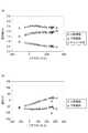
ここで、幾つかの実験の結果について説明する。まず、図3に示すように、プラズマ処理装置10Aからインピーダンス調整回路50を取り除いたプラズマ処理装置10Pを準備した。また、図4に示すように、プラズマ処理装置10Aから変圧器100Aを取り除いたプラズマ処理装置10Rを準備した。プラズマ処理装置10P及びプラズマ処理装置10Rの双方において、900sccmのアルゴン(Ar)ガスをチャンバ12cに供給し、チャンバ12cの圧力を800mTorr(106.7Pa)に設定し、高周波電源18の高周波の周波数、電力をそれぞれを450kHz、500Wに設定した。プラズマ処理装置10Pでは、種々の分配割合の設定において、分配割合と上部電極14、下部電極16、チャンバ本体12それぞれの電流値との関係、及び、分配割合と上部電極14、下部電極16それぞれの電位との関係を求めた。なお、分配割合は、変圧器100Aの二次側の総電力に対して第2の二次コイル103Aに分配される電力の割合(設定値)である。実験では、複数のタップ100tのうちグランドに接続するタップを変更することによって分配割合を設定した。また、プラズマ処理装置10Rでは、下部電極16の種々のリアクタンスの設定において、下部電極16のリアクタンスと上部電極14、下部電極16、チャンバ本体12それぞれの電流値との関係、及び、下部電極16のリアクタンスと上部電極14、下部電極16それぞれの電位との関係を求めた。なお、インピーダンス調整回路50のインピーダンスを変更することにより下部電極16のリアクタンスを設定した。 Here, the results of some experiments will be described. First, as shown in FIG. 3, a
図5の(a)に、プラズマ処理装置10Pを用いて求めた、分配割合と上部電極14、下部電極16、チャンバ本体12それぞれの電流値との関係を示し、図5の(b)に、プラズマ処理装置10Pを用いて求めた、分配割合と上部電極14、下部電極16それぞれの電位との関係を示す。また、図6の(a)に、プラズマ処理装置10Rを用いて求めた、下部電極16のリアクタンスと上部電極14、下部電極16、チャンバ本体12それぞれの電流値との関係を示し、図6の(b)に、プラズマ処理装置10Rを用いて求めた、下部電極16のリアクタンスと上部電極14、下部電極16それぞれの電位との関係を示す。 FIG. 5A shows the relationship between the distribution ratio and the current value of each of the
図5の(a)に示すように、プラズマ処理装置10Pでは、下部電極16に対する電力の分配割合が大きくなると、下部電極16に流入する電流が増大した。下部電極16に流入する電流が増大すると、図5の(b)に示すように、下部電極16の電位が負の電位となった。なお、下部電極16の電位が負の電位となり、上部電極14の電位よりも低くなると、下部電極16に向けてイオンが加速されるので、被加工物Wに入射するイオンのエネルギーが高くなる。 As shown in FIG. 5A, in the
また、図6の(a)に示すように、プラズマ処理装置10Rでは、下部電極16のインピーダンスが大きい場合には、上部電極14からプラズマに流入した電流の殆どがチャンバ本体12に流れた。下部電極16のインピーダンスが約100Ωのときに、プラズマシースのインピーダンスが打ち消されて、下部電極16に流れる電流が最大となった。図6の(a)と図6の(b)を共に参照すると、下部電極16に流れる電流が増大すると、下部電極16の電位は低くなっていた。なお、下部電極16の電位が低くなると、下部電極16に向けてイオンが加速されるので、被加工物Wに入射するイオンのエネルギーが高くなる。 As shown in FIG. 6A, in the
図5の(b)と図6の(b)を対比すると、プラズマ処理装置10Pでは、下部電極16の電位を比較的低い電位の範囲で調整することが可能であった。一方、プラズマ処理装置10Rでは、下部電極16の電位を比較的高い電位の範囲で調整することが可能であった。即ち、変圧器100Aによれば、被加工物Wに入射するイオンのエネルギーを比較的高いエネルギーの範囲で調整することが可能であることが確認された。一方、インピーダンス調整回路50によれば、被加工物Wに入射するイオンのエネルギーを比較的低いエネルギーの範囲で調整することが可能であることが確認された。 5 (b) and FIG. 6 (b), in the
また、プラズマ処理装置10Aにおいて、900sccmのアルゴン(Ar)ガスをチャンバ12cに供給し、チャンバ12cの圧力を800mTorr(106.7Pa)に設定し、高周波電源18の高周波の周波数、電力をそれぞれを450kHz、500Wに設定した。そして、種々の分配割合及び種々の下部電極16のリアクタンスの設定において、上部電極14、下部電極16、チャンバ本体12それぞれの電流値、及び、上部電極14、下部電極16それぞれの電位との関係を求めた。 Further, in the
図7の(a)に、プラズマ処理装置10Aを用いて求めた、分配割合が0%である場合の下部電極16のリアクタンスと上部電極14、下部電極16、チャンバ本体12それぞれの電流値との関係を示し、図7の(b)に、プラズマ処理装置10Aを用いて求めた、分配割合が0%である場合の下部電極16のリアクタンスと上部電極14、下部電極16それぞれの電位との関係を示す。図8の(a)に、プラズマ処理装置10Aを用いて求めた、分配割合が20%である場合の下部電極16のリアクタンスと上部電極14、下部電極16、チャンバ本体12それぞれの電流値との関係を示し、図8の(b)に、プラズマ処理装置10Aを用いて求めた、分配割合が20%である場合の下部電極16のリアクタンスと上部電極14、下部電極16それぞれの電位との関係を示す。図9の(a)に、プラズマ処理装置10Aを用いて求めた、分配割合が40%である場合の下部電極16のリアクタンスと上部電極14、下部電極16、チャンバ本体12それぞれの電流値との関係を示し、図9の(b)に、プラズマ処理装置10Aを用いて求めた、分配割合が40%である場合の下部電極16のリアクタンスと上部電極14、下部電極16それぞれの電位との関係を示す。図10の(a)に、プラズマ処理装置10Aを用いて求めた、分配割合が80%である場合の下部電極16のリアクタンスと上部電極14、下部電極16、チャンバ本体12それぞれの電流値との関係を示し、図10の(b)に、プラズマ処理装置10Aを用いて求めた、分配割合が80%である場合の下部電極16のリアクタンスと上部電極14、下部電極16それぞれの電位との関係を示す。なお、分配割合が0%である場合は、プラズマ処理装置10Rと同等の環境であるので、図6の(a)と図7の(a)は同一であり、図6の(b)と図7の(b)とは同一になっている。 FIG. 7A shows the relationship between the reactance of the
図7の(a)、図8の(a)、図9の(a)、及び、図10の(a)に示すように、プラズマ処理装置10Aにおいても、分配比率が大きくなるにつれて、下部電極16に流れる電流が増大した。また、図7の(b)、図8の(b)、図9の(b)、及び、図10の(b)に示すように、分配比率が大きくなるにつれて、下部電極16の電位が低くなっていた。また、分配比率が大きくなるにつれて、下部電極16の電位が上部電極14の電位よりも低くなっていた。したがって、プラズマ処理装置10Aによれば、変圧器100Aによる電力の分配により、比較的高いエネルギーの範囲で被加工物Wに入射するイオンのエネルギーを調整することが可能であることが確認された。また、図7の(b)及び図8の(b)に示すように、下部電極16のインピーダンスの調整により、下部電極16の電位を比較的高い電位の範囲で調整することが可能であることが確認された。したがって、プラズマ処理装置10Aによれば、インピーダンス調整回路50のインピーダンスの調整により、比較的低いエネルギーの範囲で被加工物Wに入射するイオンのエネルギーを調整することが可能であることが確認された。故に、プラズマ処理装置10Aによれば、下部電極16の上に配置された被加工物Wに入射するイオンのエネルギーの調整可能な範囲が広くなる。 As shown in (a) of FIG. 7, (a) of FIG. 8, (a) of FIG. 9, and (a) of FIG. 10, even in the
次に、図11を参照し、別の実施形態に係るプラズマ処理装置について説明する。図11は、別の実施形態に係るプラズマ処理装置を示す図である。以下、図11に示すプラズマ処理装置10Bがプラズマ処理装置10Aと異なる点について説明し、重複する説明を省略する。 Next, a plasma processing apparatus according to another embodiment will be described with reference to FIG. FIG. 11 is a diagram illustrating a plasma processing apparatus according to another embodiment. Hereinafter, points of the
プラズマ処理装置10Bは、変圧器100Aではなく、変圧器100Bを備えている。また、プラズマ処理装置10Bは、追加のインピーダンス調整回路51を更に備えている。インピーダンス調整回路51は、可変コンデンサ及び/又はインダクタを有し得る。プラズマ処理装置10Bでは、インピーダンス調整回路51は、可変コンデンサ51a及びインダクタ51bを有する。可変コンデンサ51a及びインダクタ51bは、上部電極14と変圧器100Bの端子102aとの間で直列接続されている。なお、インピーダンス調整回路51は、グランドに接続された素子を有していない。高周波電源18は、整合器38を介して変圧器100Bの端子101aに接続されている。インピーダンス調整回路50は、下部電極16と変圧器100Bの端子103aとの間で接続されている。変圧器100Bの端子102bと端子103bはグランドに接続されている。 The
図12は、図11に示すプラズマ処理装置10Bの変圧器100Bを一部破断して示す斜視図である。図13は、図12に示す変圧器100Bの三つのコイルを概略的に示す図である。図12及び図13に示す変圧器100Bは、回転軸112、一次コイル101B、第1の二次コイル102B、及び、第2の二次コイル103Bを備えている。第1の二次コイル102B、及び、第2の二次コイル103Bは、二次側コイル対106を構成している。一実施形態において、変圧器100Bは、支持部材122,124、支柱126、支持部材128,130、支持部材132,134、端子101a,101b、端子102a,102b、及び、端子103a,103bを更に備えている。 FIG. 12 is a perspective view showing a partially
回転軸112は、略円柱状をなしている。回転軸112は、その中心軸線RX周りに、即ち、中心軸線RXを回転軸線として、回転可能に設けられている。一実施形態では、回転軸112は、支持部材122と支持部材124によって回転可能に支持されている。支持部材122及び支持部材124は、板状の部材であり、略矩形の平面形状を有する。支持部材122及び支持部材124は、絶縁体から形成されている。支持部材122及び支持部材124は、中心軸線RXに交差又は略直交するように設けられており、それらの板厚方向が中心軸線RXが延びる方向RDに略一致するよう、方向RDに沿って配列されている。支持部材122の隅部には支柱126の一端が固定されており、支持部材124の隅部には支柱126の他端が固定されている。回転軸112の一端部は、支持部材122を貫通して、支持部材122から突出している。この回転軸112の一端部は、駆動機構(例えば、モータ)に接続されている。 The
支持部材128及び支持部材130は、略円盤状の部材であり、絶縁体から形成されている。支持部材128及び支持部材130は、支持部材122と支持部材124との間において中心軸線RXに交差又は略直交するように設けられており、それらの板厚方向が方向RDに略一致するように方向RDに沿って配列されている。また、支持部材132及び支持部材134は、略円盤状の部材であり、絶縁体から形成されている。支持部材132及び支持部材134は、支持部材128と支持部材130との間において中心軸線RXに交差又は略直交するように設けられており、それらの板厚方向が方向RDに略一致するように方向RDに沿って配列されている。回転軸112は、支持部材128,130,132,134それぞれの中心を貫通している。支持部材128,130,132,134は、回転軸112に固定されている。 The
一次コイル101Bは、中心軸線RXに直交する第1の軸線AX1周りに延在している。一実施形態では、第1の軸線AX1は、支持部材122と支持部材124との中間において中心軸線RXに直交している。一次コイル101Bは、支持部材122の外側と支持部材124の外側を交互に通るように、第1の軸線AX1中心に巻かれている。 The
一次コイル101Bの一端は、端子101aに接続されている。一実施形態では、端子101aは、支持部材122の一面122a(変圧器100Bの外側に向いた面)に設けられている。また、一次コイル101Bの他端は、端子101bに接続されている。一実施形態では、端子101bは、支持部材124の一面124a(変圧器100Bの外側に向いた面)に設けられている。 One end of the
第1の二次コイル102Bは、第2の軸線AX2周りに延在している。第2の軸線AX2は、一次コイル101Bによって囲まれた領域内で中心軸線RXに直交している。一実施形態では、第2の軸線AX2は、支持部材128と支持部材130との中間において中心軸線RXに直交している。第1の二次コイル102Bは、支持部材128の外側と支持部材130の外側を交互に通るように、第2の軸線AX2中心に巻かれている。第1の二次コイル102Bは、支持部材128及び支持部材130を介して回転軸112によって支持されている。 The first
第1の二次コイル102Bの一端は、端子102aに接続されている。また、第1の二次コイル102Bの他端は、端子102bに接続されている。一実施形態では、端子102a及び端子102bは、支持部材122の一面122aに設けられている。回転軸112は、同軸状に設けられた第1の導体と第2の導体を含んでおり、第1の二次コイル102Bの一端は第1の導体に接続されており、第1の二次コイル102Bの他端は第2の導体に接続されている。第1の導体は、ロータリーコネクタ140内のスリップリングを介して端子102aに接続されている。また、第2の導体は、ロータリーコネクタ140内の別のスリップリングを介して端子102bに接続されている。 One end of the first
第2の二次コイル103Bは、第3の軸線AX3周りに延在している。第3の軸線AX3は、一次コイル101Bによって囲まれた領域内で中心軸線RXに直交している。また、第3の軸線AX3は、第2の軸線AX2に交差している。第3の軸線AX3と第2の軸線AX2は、互いの間に所定の角度θpをなしている。角度θpは、限定されるものではないが、例えば、90度である。一実施形態では、第3の軸線AX3は、支持部材132と支持部材134との中間において中心軸線RXに直交している。第2の二次コイル103Bは、支持部材132の外側と支持部材134の外側を交互に通るように、第3の軸線AX3中心に巻かれている。第2の二次コイル103Bは、支持部材132及び支持部材134を介して回転軸112によって支持されている。この第2の二次コイル103Bと第1の二次コイル102Bとの間には、絶縁距離が確保されている。 The second
第2の二次コイル103Bの一端は、端子103aに接続されている。また、第2の二次コイル103Bの他端は、端子103bに接続されている。一実施形態では、端子103a及び端子103bは、支持部材124の一面124aに設けられている。回転軸112は、同軸状に設けられた第3の導体と第4の導体を含んでおり、第2の二次コイル103Bの一端は第3の導体に接続されており、第2の二次コイル103Bの他端は第4の導体に接続されている。第3の導体は、支持部材124の近傍に設けられた別のロータリーコネクタのスリップリングを介して端子103aに接続されている。また、第4の導体は、当該別のロータリーコネクタ内の別のスリップリングを介して端子103bに接続されている。 One end of the second
変圧器100Bでは、一次コイル101Bに高周波電源18からの高周波が供給されると、一次コイル101Bが第1の軸線AX1が延びる方向に略平行な方向に磁束が発生する。また、二次側コイル対106の回転角度を調整することにより、第1の二次コイル102Bを貫く磁束の量、及び、第2の二次コイル103Bを貫く磁束の量が変化する。第1の二次コイル102Bには、それを貫く磁束の量に応じた誘導起電力が生じる。また、第2の二次コイル103Bには、それを貫く磁束の量に応じた誘導起電力が生じる。したがって、変圧器100Bによれば、第1の二次コイル102Bに分配される高周波の電力と第2の二次コイル103Bに分配される高周波の電力の比が調整され得る。かかる変圧器100Bを有するプラズマ処理装置10Bによれば、プラズマ処理装置10Aと同様に、下部電極16の上に配置された被加工物Wに入射するイオンのエネルギーの調整可能な範囲が広くなる。 In the
次に、図14を参照し、更に別の実施形態に係るプラズマ処理装置について説明する。図14は、更に別の実施形態に係るプラズマ処理装置を示す図である。以下、図14に示すプラズマ処理装置10Cがプラズマ処理装置10Aと異なる点について説明し、重複する説明を省略する。 Next, a plasma processing apparatus according to another embodiment will be described with reference to FIG. FIG. 14 is a diagram showing a plasma processing apparatus according to still another embodiment. Hereinafter, the points of the
プラズマ処理装置10Cでは、インピーダンス調整回路50が、複数のタップ100tとグランドとの間で接続されている。このように、インピーダンス調整回路50は、下部電極16と変圧器100Aの二次側のコイルが接続されるグランドとの間の直列回路に設けられ得る。 In the
次に、図15を参照し、更に別の実施形態に係るプラズマ処理装置について説明する。図15は、更に別の実施形態に係るプラズマ処理装置を示す図である。以下、図15に示すプラズマ処理装置10Dがプラズマ処理装置10Bと異なる点について説明し、重複する説明を省略する。 Next, a plasma processing apparatus according to another embodiment will be described with reference to FIG. FIG. 15 is a diagram illustrating a plasma processing apparatus according to yet another embodiment. Hereinafter, the points of the
プラズマ処理装置10Dでは、インピーダンス調整回路50が端子103bとグランドとの間で接続されている。また、インピーダンス調整回路51が端子102bと別のグランドとの間で接続されている。このように、第1の二次コイル102Bと第2の二次コイル103Bが別個のグランドに接続されている場合には、第1の二次コイル102Bとグランドとの間、及び、第2の二次コイル103Bとグランドとの間に、個別にインピーダンス調整回路が設けられてもよい。 In the
次に、図16及び図17を参照し、更に別の実施形態に係るプラズマ処理装置について説明する。図16は、更に別の実施形態に係るプラズマ処理装置を示す図である。図17は、図16に示すプラズマ処理装置の変圧器を示す図である。以下、図16に示すプラズマ処理装置10Eがプラズマ処理装置10Aと異なる点について説明し、重複する説明を省略する。 Next, a plasma processing apparatus according to yet another embodiment will be described with reference to FIGS. FIG. 16 is a diagram illustrating a plasma processing apparatus according to yet another embodiment. FIG. 17 is a diagram showing a transformer of the plasma processing apparatus shown in FIG. Hereinafter, the points of the
プラズマ処理装置10Eは、変圧器100Aではなく、変圧器100Eを備えている。変圧器100Eは、一次コイル101E、第1の二次コイル102E、及び、第2の二次コイル103Eを備えている。一次コイル101Eは、一次コイル101Aと同様のコイルである。一次コイル101Eの一端は端子101aであり、整合器38を介して高周波電源18に接続されている。一次コイル101Eの他端は、端子101bであり、高周波電源18に接続されており、接地されている。 The
第1の二次コイル102E及び第2の二次コイル103Eは、第1の二次コイル102A及び第2の二次コイル103Aと同様に、単一のコイルから形成されている。この単一のコイルの中間のノード101nは端子101eに接続されている。端子101eはグランドに接続されている。ノード101nに対して単一のコイルの一方側の部分は第1の二次コイル102Eであり、ノード101nに対して単一のコイルの他方側の部分は第2の二次コイル103Eである。第1の二次コイル102Eの一端は端子102aであり、インピーダンス調整回路50を介して上部電極14に接続されている。また、第2の二次コイル103Eの一端は端子103aであり、コンデンサ60を介して下部電極16に接続されている。この変圧器100Eでは、単一のコイルの巻き線において接地される箇所が固定されている。したがって、第1の二次コイル102Eの巻き数と第2の二次コイル103Eの巻き数の比は一定である。 The first
ここで、一次コイルに高周波電源が接続され、二次コイルに複素インピーダンスZ2の負荷が接続されている場合には、一次コイルの電流値と二次コイルの電流値との比は、以下の式(3)で表される。式(3)において、L1は一次コイルの自己インダクタンス、L2は二次コイルの自己インダクタンス、kは一次コイルと二次コイルの間の結合係数、ωは高周波の角周波数である。なお、複素インピーダンスZ2は、プラズマのインピーダンスと二次コイルとプラズマとの間の給電回路のインピーダンスである。
式(3)の分母が小さくなるように、即ち、二次側で直列共振が生じるように複素インピーダンスZ2を調整すると、二次側に流れる電流の値が大きくなる。一方、式(3)の分母が大きくなるように複素インピーダンスZ2を調整すると、二次側に流れる電流の値が小さくなる。変圧器100Eでは、二つの二次コイルのうち一方の二次コイルに流れる電流が大きくなり、一方の二次コイルに分配される高周波の電力が増大すると、他方の二次コイルに分配される高周波の電力は小さくなる。したがって、二つの二次コイルを構成する単一のコイルの接地箇所が固定されていても、インピーダンス調整回路50によるインピーダンスの調整により、上部電極14に供給される高周波の電力と下部電極16に供給される高周波の電力を調整することが可能である。故に、プラズマ処理装置10Eによれば、下部電極16に入射するイオンのエネルギーを調整することが可能である。As the denominator of Equation (3) is reduced, i.e., adjusting the complex impedance Z2 to the series resonance occurs at the secondary side, the value of the current flowing through the secondary side increases. On the other hand, adjusting the complex impedance Z2 as the denominator of equation (3) increases, the value of the current flowing through the secondary side is reduced. In the
以下、プラズマ処理装置10Eの評価のために行った実験の結果について説明する。この実験に用いた変圧器100Eの一次コイル101Eは、直径が42mm、巻き数が27のコイルであった。また、第1の二次コイル102E及び第2の二次コイル103Eを構成する単一のコイルも、直径42mm、巻き数27のコイルであった。この単一のコイルは13ターン目をグランドに接続した。そして、600sccmのアルゴン(Ar)ガスをチャンバ12cに供給し、チャンバ12cの圧力を800mTorr(106.7Pa)に設定し、高周波電源18の高周波の周波数、電力をそれぞれを13.56MHz、200Wに設定した。さらに、インピーダンス調整回路50の可変コンデンサ50aのダイアル値を変更して、インピーダンス調整回路50のインピーダンスを種々のインピーダンスに設定しつつ、チャンバ本体12、上部電極14、及び、下部電極16それぞれの電流、上部電極14及び下部電極16それぞれの高周波電圧、並びに、上部電極14及び下部電極16それぞれの直流電位を測定した。 Hereinafter, results of an experiment performed for evaluating the
図18の(a)に、可変コンデンサ50aのダイアル値とチャンバ本体12、上部電極14、及び、下部電極16それぞれの電流との関係を示し、図18の(b)に、可変コンデンサ50aのダイアル値と上部電極14及び下部電極16それぞれの直流電位との関係を示す。 FIG. 18A shows the relationship between the dial value of the
実験に用いたインピーダンス調整回路50では、可変コンデンサ50aのダイアル値が8近傍であるときに、第1の二次コイル102Eのインピーダンス、インピーダンス調整回路50のインピーダンス、及び、上部電極14のプラズマ負荷のインピーダンスが直列共振状態になった。即ち、式(3)に示した分母がゼロの状態になった。この直列共振状態では、上部電極14のみに電流が流れており、下部電極16には電流が殆ど流れていなかった。可変コンデンサ50aのダイアル値が8より小さい状態では、式(3)の分母は正となり、可変コンデンサ50aのダイアル値が8より大きい状態では、式(3)の分母は負となる。したがって、上部電極14から下部電極16に流れる電流の向きを同位相の向きとすると、可変コンデンサ50aのダイアル値が8より小さい状態では逆位相の電流が流れ、可変コンデンサ50aのダイアル値が8より大きい状態では同位相の電流が流れていた。このように、インピーダンス調整回路50により、上部電極14と下部電極16へ供給される電力比を調整することが可能であると言える。 In the
図18の(a)に示すように、可変コンデンサ50aのダイアル値を8よりも更に大きい値に設定したところ、上部電極14の電流値が減少し、下部電極16の電流値が増大した。また、可変コンデンサ50aのダイアル値が8よりも大きいある値であるときに、上部電極14の電流値と下部電極16の電流値が略同一となり、チャンバ本体12に流れる電流が最小になった。したがって、可変コンデンサ50aのダイアル値がかかる値に設定されたときには、プラズマが上部電極14と下部電極16との間に閉じ込められていることになる。故に、可変コンデンサ50aの調整によって、プラズマを安定して生成することが可能であることが確認された。 As shown in FIG. 18A, when the dial value of the
また、図18の(b)に示すように、可変コンデンサ50aのダイアル値に応じて、下部電極16の直流電位は、負の電位から正の電位まで大きく変化した。したがって、プラズマ処理装置10Eでは、下部電極16の上に配置された被加工物に入射するイオンのエネルギーの調整可能な範囲が広いことが確認された。 Further, as shown in FIG. 18B, the DC potential of the
以上、種々の実施形態について説明してきたが、上述した実施形態に限定されることなく種々の変形態様を構成可能である。例えば、インピーダンス調整回路が配置される箇所は、上述した実施形態において当該インピーダンス調整回路が配置された箇所に限定されるものではない。インピーダンス調整回路は、上部電極14と第1の二次コイルの他端に接続されたグランドとの間の直列回路、及び、下部電極16と第2の二次コイルの他端に接続されたグランドとの間の直列回路のうち一方又は双方において適所に設けることが可能である。 Although various embodiments have been described above, various modifications can be made without being limited to the above embodiments. For example, the location where the impedance adjustment circuit is arranged is not limited to the location where the impedance adjustment circuit is arranged in the above-described embodiment. The impedance adjustment circuit includes a series circuit between the
10A,10B,10C,10D,10E…プラズマ処理装置、12…チャンバ本体、12c…チャンバ、14…上部電極、16…下部電極、18…高周波電源、20…ステージ、32…ガス供給部、36…排気装置、38…整合器、50,51…インピーダンス調整回路、100A,100B,100E…変圧器、101A,101B,101E…一次コイル、102A,102B,102E…第1の二次コイル、103A,103B,103E…第2の二次コイル。 10A, 10B, 10C, 10D, 10E: Plasma processing apparatus, 12: Chamber main body, 12c: Chamber, 14: Upper electrode, 16: Lower electrode, 18: High frequency power supply, 20: Stage, 32: Gas supply unit, 36 ... Exhaust device, 38 Matching device, 50, 51 Impedance adjusting circuit, 100A, 100B, 100E Transformer, 101A, 101B, 101E Primary coil, 102A, 102B, 102E First secondary coil, 103A, 103B , 103E ... second secondary coil.
Claims (9)
Translated fromJapaneseチャンバを提供するチャンバ本体と、
前記チャンバ内の空間がそれらの間に介在するように設けられた第1の電極及び第2の電極と、
高周波電源と、
前記高周波電源に接続されたインピーダンス整合用の整合器と、
前記高周波電源に前記整合器を介して接続された一次コイル、並びに、第1の二次コイル及び第2の二次コイルを有する変圧器であり、該第1の二次コイルの一端は前記第1の電極に接続されており、該第2の二次コイルの一端は前記第2の電極に接続された、該変圧器と、
可変のインピーダンスを有し、前記第1の電極と前記第1の二次コイルの他端に接続されたグランドとの間の直列回路、及び、前記第2の電極と前記第2の二次コイルの他端に接続されたグランドとの間の直列回路のうち少なくとも一方に設けられた少なくとも一つのインピーダンス調整回路と、
を備えるプラズマ処理装置。A capacitively-coupled plasma processing apparatus,
A chamber body providing a chamber;
A first electrode and a second electrode provided so that a space in the chamber is interposed therebetween;
A high frequency power supply,
A matching device for impedance matching connected to the high-frequency power supply,
A primary coil connected to the high-frequency power supply via the matching device, and a transformer having a first secondary coil and a second secondary coil, one end of the first secondary coil being One end of the second secondary coil is connected to the first electrode, and one end of the second secondary coil is connected to the second electrode;
A series circuit having a variable impedance between the first electrode and a ground connected to the other end of the first secondary coil; and a second circuit including the second electrode and the second secondary coil. At least one impedance adjustment circuit provided in at least one of the series circuit between the ground connected to the other end of the
A plasma processing apparatus comprising:
前記第1の二次コイルの巻き線は、該第1の二次コイルと前記一次コイルが断面を共有するように、前記一次コイルの中心軸線の周りで巻かれており、
前記第2の二次コイルの巻き線は、該第2の二次コイルと前記一次コイルが断面を共有するように、前記中心軸線の周りで巻かれており、
前記第1の二次コイル及び前記第2の二次コイルは、グランドに選択的に接続可能な複数のタップを有する単一のコイルから形成される、
請求項1に記載のプラズマ処理装置。The primary coil, the first secondary coil, and the second secondary coil are provided coaxially,
Windings of the first secondary coil are wound around a central axis of the primary coil such that the first secondary coil and the primary coil share a cross section;
The winding of the second secondary coil is wound around the central axis such that the second secondary coil and the primary coil share a cross section,
The first secondary coil and the second secondary coil are formed from a single coil having a plurality of taps selectively connectable to ground;
The plasma processing apparatus according to claim 1.
前記一次コイルは、前記中心軸線に直交する第1の軸線の周りで延在し、
前記第1の二次コイルは、第2の軸線の周りで延在し、前記回転軸によって支持されており、該第2の軸線は前記一次コイルによって囲まれた領域内で前記中心軸線に直交しており、
前記第2の二次コイルは、第3の軸線周りに延在し、前記回転軸によって支持されており、該第3の軸線は、前記領域内で前記中心軸線に直交し且つ前記第2の軸線と所定の角度をなしている、
請求項1に記載のプラズマ処理装置。The transformer further has a rotating shaft rotatable with its center axis as a rotating axis,
The primary coil extends around a first axis orthogonal to the central axis;
The first secondary coil extends around a second axis and is supported by the axis of rotation, the second axis being orthogonal to the central axis within a region surrounded by the primary coil. And
The second secondary coil extends around a third axis and is supported by the rotational axis, wherein the third axis is orthogonal to the central axis within the region and the second axis. At a predetermined angle with the axis,
The plasma processing apparatus according to claim 1.
前記第1の二次コイルの巻き線は、該第1の二次コイルと前記一次コイルが断面を共有するように、前記一次コイルの中心軸線の周りで巻かれており、
前記第2の二次コイルの巻き線は、該第2の二次コイルと前記一次コイルが断面を共有するように、前記中心軸線の周りで巻かれており、
前記第1の二次コイル及び前記第2の二次コイルは、その中間において接地された単一のコイルから形成されている、
請求項1に記載のプラズマ処理装置。The primary coil, the first secondary coil, and the second secondary coil are provided coaxially,
The winding of the first secondary coil is wound around a central axis of the primary coil such that the first secondary coil and the primary coil share a cross section,
The winding of the second secondary coil is wound around the central axis such that the second secondary coil and the primary coil share a cross section,
The first secondary coil and the second secondary coil are formed from a single coil grounded in between.
The plasma processing apparatus according to claim 1.
Priority Applications (4)
| Application Number | Priority Date | Filing Date | Title |
|---|---|---|---|
| JP2016099568AJP6630630B2 (en) | 2016-05-18 | 2016-05-18 | Plasma processing equipment |
| US15/593,861US10593517B2 (en) | 2016-05-18 | 2017-05-12 | Plasma processing apparatus |
| KR1020170060168AKR101974268B1 (en) | 2016-05-18 | 2017-05-15 | Plasma processing apparatus |
| CN201710353096.3ACN107403711B (en) | 2016-05-18 | 2017-05-18 | Plasma processing apparatus |
Applications Claiming Priority (1)
| Application Number | Priority Date | Filing Date | Title |
|---|---|---|---|
| JP2016099568AJP6630630B2 (en) | 2016-05-18 | 2016-05-18 | Plasma processing equipment |
Publications (2)
| Publication Number | Publication Date |
|---|---|
| JP2017208225A JP2017208225A (en) | 2017-11-24 |
| JP6630630B2true JP6630630B2 (en) | 2020-01-15 |
Family
ID=60330352
Family Applications (1)
| Application Number | Title | Priority Date | Filing Date |
|---|---|---|---|
| JP2016099568AActiveJP6630630B2 (en) | 2016-05-18 | 2016-05-18 | Plasma processing equipment |
Country Status (4)
| Country | Link |
|---|---|
| US (1) | US10593517B2 (en) |
| JP (1) | JP6630630B2 (en) |
| KR (1) | KR101974268B1 (en) |
| CN (1) | CN107403711B (en) |
Families Citing this family (27)
| Publication number | Priority date | Publication date | Assignee | Title |
|---|---|---|---|---|
| JP6595002B2 (en)* | 2017-06-27 | 2019-10-23 | キヤノンアネルバ株式会社 | Sputtering equipment |
| US12288673B2 (en) | 2017-11-29 | 2025-04-29 | COMET Technologies USA, Inc. | Retuning for impedance matching network control |
| US11290080B2 (en) | 2017-11-29 | 2022-03-29 | COMET Technologies USA, Inc. | Retuning for impedance matching network control |
| US11527385B2 (en) | 2021-04-29 | 2022-12-13 | COMET Technologies USA, Inc. | Systems and methods for calibrating capacitors of matching networks |
| US11114279B2 (en)* | 2019-06-28 | 2021-09-07 | COMET Technologies USA, Inc. | Arc suppression device for plasma processing equipment |
| US11107661B2 (en) | 2019-07-09 | 2021-08-31 | COMET Technologies USA, Inc. | Hybrid matching network topology |
| US11596309B2 (en) | 2019-07-09 | 2023-03-07 | COMET Technologies USA, Inc. | Hybrid matching network topology |
| US10910196B1 (en)* | 2019-07-24 | 2021-02-02 | Tokyo Electron Limited | Mode-switching plasma systems and methods of operating thereof |
| EP4022656A4 (en) | 2019-08-28 | 2023-10-04 | Comet Technologies USA, Inc | HIGH POWER LOW FREQUENCY COILS |
| US11830708B2 (en) | 2020-01-10 | 2023-11-28 | COMET Technologies USA, Inc. | Inductive broad-band sensors for electromagnetic waves |
| US11887820B2 (en) | 2020-01-10 | 2024-01-30 | COMET Technologies USA, Inc. | Sector shunts for plasma-based wafer processing systems |
| US12027351B2 (en) | 2020-01-10 | 2024-07-02 | COMET Technologies USA, Inc. | Plasma non-uniformity detection |
| US11521832B2 (en) | 2020-01-10 | 2022-12-06 | COMET Technologies USA, Inc. | Uniformity control for radio frequency plasma processing systems |
| US11670488B2 (en) | 2020-01-10 | 2023-06-06 | COMET Technologies USA, Inc. | Fast arc detecting match network |
| US11961711B2 (en) | 2020-01-20 | 2024-04-16 | COMET Technologies USA, Inc. | Radio frequency match network and generator |
| US11605527B2 (en) | 2020-01-20 | 2023-03-14 | COMET Technologies USA, Inc. | Pulsing control match network |
| US11373844B2 (en) | 2020-09-28 | 2022-06-28 | COMET Technologies USA, Inc. | Systems and methods for repetitive tuning of matching networks |
| TW202226897A (en)* | 2020-11-06 | 2022-07-01 | 日商東京威力科創股份有限公司 | Filter circuit |
| US12057296B2 (en) | 2021-02-22 | 2024-08-06 | COMET Technologies USA, Inc. | Electromagnetic field sensing device |
| US11923175B2 (en) | 2021-07-28 | 2024-03-05 | COMET Technologies USA, Inc. | Systems and methods for variable gain tuning of matching networks |
| CN114501765A (en)* | 2022-01-26 | 2022-05-13 | 江苏神州半导体科技有限公司 | Gas dissociation circuit and gas dissociation system based on multi-coil coupling |
| US12243717B2 (en) | 2022-04-04 | 2025-03-04 | COMET Technologies USA, Inc. | Variable reactance device having isolated gate drive power supplies |
| US11657980B1 (en) | 2022-05-09 | 2023-05-23 | COMET Technologies USA, Inc. | Dielectric fluid variable capacitor |
| US12040139B2 (en) | 2022-05-09 | 2024-07-16 | COMET Technologies USA, Inc. | Variable capacitor with linear impedance and high voltage breakdown |
| US12051549B2 (en) | 2022-08-02 | 2024-07-30 | COMET Technologies USA, Inc. | Coaxial variable capacitor |
| US12132435B2 (en) | 2022-10-27 | 2024-10-29 | COMET Technologies USA, Inc. | Method for repeatable stepper motor homing |
| US20250266281A1 (en)* | 2024-02-15 | 2025-08-21 | Advanced Energy Industries, Inc. | Electrostatic wafer clamping and sensing system |
Family Cites Families (24)
| Publication number | Priority date | Publication date | Assignee | Title |
|---|---|---|---|---|
| US2087636A (en) | 1932-11-25 | 1937-07-20 | William C Baumann | Electrical apparatus |
| JPS5546862A (en) | 1978-09-25 | 1980-04-02 | Okuma Mach Works Ltd | Multipolar resolver |
| US4612527A (en) | 1984-08-10 | 1986-09-16 | United Kingdom Atomic Energy Authority | Electric power transfer system |
| GB8714216D0 (en)* | 1987-06-17 | 1987-07-22 | Hiden Analytical Ltd | Power supply circuits |
| US4871421A (en)* | 1988-09-15 | 1989-10-03 | Lam Research Corporation | Split-phase driver for plasma etch system |
| JP3016821B2 (en)* | 1990-06-15 | 2000-03-06 | 東京エレクトロン株式会社 | Plasma processing method |
| JPH06244151A (en)* | 1993-02-16 | 1994-09-02 | Tokyo Electron Ltd | Plasma treating device |
| US5519275A (en) | 1994-03-18 | 1996-05-21 | Coleman Powermate, Inc. | Electric machine with a transformer having a rotating component |
| JP3016821U (en) | 1995-04-11 | 1995-10-09 | 洋治 喜多 | Frozen fish meat for raw consumption |
| US5783984A (en) | 1995-06-16 | 1998-07-21 | Hughes Electronics | Method and means for combining a transformer and inductor on a single core structure |
| US6118201A (en) | 1997-03-07 | 2000-09-12 | American Precision Industries Inc. | Resolver with leakage flux absorber |
| JP3951557B2 (en)* | 2000-05-26 | 2007-08-01 | 松下電工株式会社 | Plasma processing apparatus and plasma processing method |
| JP4819244B2 (en) | 2001-05-15 | 2011-11-24 | 東京エレクトロン株式会社 | Plasma processing equipment |
| US6706138B2 (en)* | 2001-08-16 | 2004-03-16 | Applied Materials Inc. | Adjustable dual frequency voltage dividing plasma reactor |
| US20050258148A1 (en)* | 2004-05-18 | 2005-11-24 | Nordson Corporation | Plasma system with isolated radio-frequency powered electrodes |
| JP5270576B2 (en) | 2007-01-11 | 2013-08-21 | プラナーマグ インコーポレイテッド | Flat type wideband transformer |
| JP5371238B2 (en) | 2007-12-20 | 2013-12-18 | 東京エレクトロン株式会社 | Plasma processing apparatus and plasma processing method |
| US7825537B2 (en) | 2008-11-14 | 2010-11-02 | Harris Corporation | Inductive power transfer system and method |
| JP2013098177A (en)* | 2011-10-31 | 2013-05-20 | Semes Co Ltd | Substrate processing device and impedance matching method |
| CN103377869B (en)* | 2012-04-16 | 2016-02-10 | 北京北方微电子基地设备工艺研究中心有限责任公司 | Impedance matching methods, impedance matching system and plasma processing device |
| CN103256930B (en) | 2013-05-15 | 2015-06-17 | 重庆华渝电气仪表总厂 | High-reliability inertia bearing keeping system |
| CN104349567A (en) | 2013-07-29 | 2015-02-11 | 北京北方微电子基地设备工艺研究中心有限责任公司 | Radio frequency power supply system and a method for performing impedance matching by utilizing radio frequency power supply system |
| US9793046B2 (en) | 2013-10-24 | 2017-10-17 | Rosemount Aerospace Inc. | Rotating transformers for electrical machines |
| KR20150048551A (en) | 2013-10-28 | 2015-05-07 | 삼성전기주식회사 | Transformer, power supplying apparatus, display apparatus having thereof |
- 2016
- 2016-05-18JPJP2016099568Apatent/JP6630630B2/enactiveActive
- 2017
- 2017-05-12USUS15/593,861patent/US10593517B2/enactiveActive
- 2017-05-15KRKR1020170060168Apatent/KR101974268B1/enactiveActive
- 2017-05-18CNCN201710353096.3Apatent/CN107403711B/enactiveActive
Also Published As
| Publication number | Publication date |
|---|---|
| US20170338081A1 (en) | 2017-11-23 |
| KR101974268B1 (en) | 2019-04-30 |
| CN107403711B (en) | 2019-07-05 |
| JP2017208225A (en) | 2017-11-24 |
| US10593517B2 (en) | 2020-03-17 |
| CN107403711A (en) | 2017-11-28 |
| KR20170130296A (en) | 2017-11-28 |
Similar Documents
| Publication | Publication Date | Title |
|---|---|---|
| JP6630630B2 (en) | Plasma processing equipment | |
| US11508554B2 (en) | High voltage filter assembly | |
| CN104994676B (en) | Plasma processing apparatus | |
| JP4750879B2 (en) | Plasma generator | |
| TWI585847B (en) | Plasma processing device and plasma processing method | |
| WO2020076413A1 (en) | Rf antenna producing a uniform near-field poynting vector | |
| JP6745134B2 (en) | Plasma processing device | |
| JP6530859B2 (en) | Plasma processing system | |
| CN111512404B (en) | High-power radio frequency spiral coil filter | |
| KR101963954B1 (en) | Transformer, plasma processing apparatus, and plasma processing method |
Legal Events
| Date | Code | Title | Description |
|---|---|---|---|
| A621 | Written request for application examination | Free format text:JAPANESE INTERMEDIATE CODE: A621 Effective date:20190201 | |
| A977 | Report on retrieval | Free format text:JAPANESE INTERMEDIATE CODE: A971007 Effective date:20191106 | |
| TRDD | Decision of grant or rejection written | ||
| A01 | Written decision to grant a patent or to grant a registration (utility model) | Free format text:JAPANESE INTERMEDIATE CODE: A01 Effective date:20191112 | |
| A61 | First payment of annual fees (during grant procedure) | Free format text:JAPANESE INTERMEDIATE CODE: A61 Effective date:20191209 | |
| R150 | Certificate of patent or registration of utility model | Ref document number:6630630 Country of ref document:JP Free format text:JAPANESE INTERMEDIATE CODE: R150 | |
| R250 | Receipt of annual fees | Free format text:JAPANESE INTERMEDIATE CODE: R250 | |
| R250 | Receipt of annual fees | Free format text:JAPANESE INTERMEDIATE CODE: R250 | |
| R250 | Receipt of annual fees | Free format text:JAPANESE INTERMEDIATE CODE: R250 |