JP6619471B2 - Calibration of internal integrated circuit resistance - Google Patents
Calibration of internal integrated circuit resistanceDownload PDFInfo
- Publication number
- JP6619471B2 JP6619471B2JP2018088746AJP2018088746AJP6619471B2JP 6619471 B2JP6619471 B2JP 6619471B2JP 2018088746 AJP2018088746 AJP 2018088746AJP 2018088746 AJP2018088746 AJP 2018088746AJP 6619471 B2JP6619471 B2JP 6619471B2
- Authority
- JP
- Japan
- Prior art keywords
- sensor
- resistor
- resistance value
- circuit
- calibration
- Prior art date
- Legal status (The legal status is an assumption and is not a legal conclusion. Google has not performed a legal analysis and makes no representation as to the accuracy of the status listed.)
- Active
Links
- 230000005284excitationEffects0.000claimsdescription56
- 238000005259measurementMethods0.000claimsdescription40
- 230000004044responseEffects0.000claimsdescription33
- 238000000034methodMethods0.000claimsdescription19
- 230000003993interactionEffects0.000claims1
- 238000010586diagramMethods0.000description13
- 239000007789gasSubstances0.000description11
- 230000008859changeEffects0.000description4
- 101100382340Arabidopsis thaliana CAM2 geneProteins0.000description2
- 101100494530Brassica oleracea var. botrytis CAL-A geneProteins0.000description2
- 101100165913Brassica oleracea var. italica CAL geneProteins0.000description2
- 101150118283CAL1 geneProteins0.000description2
- 102100021849CalretininHuman genes0.000description2
- 101000898072Homo sapiens CalretininProteins0.000description2
- 101100029577Saccharomyces cerevisiae (strain ATCC 204508 / S288c) CDC43 geneProteins0.000description2
- 101100439683Saccharomyces cerevisiae (strain ATCC 204508 / S288c) CHS3 geneProteins0.000description2
- 101150014174calm geneProteins0.000description2
- 238000006243chemical reactionMethods0.000description2
- 230000036541healthEffects0.000description2
- 239000004065semiconductorSubstances0.000description2
- UGFAIRIUMAVXCW-UHFFFAOYSA-NCarbon monoxideChemical compound[O+]#[C-]UGFAIRIUMAVXCW-UHFFFAOYSA-N0.000description1
- LFQSCWFLJHTTHZ-UHFFFAOYSA-NEthanolChemical compoundCCOLFQSCWFLJHTTHZ-UHFFFAOYSA-N0.000description1
- QVGXLLKOCUKJST-UHFFFAOYSA-Natomic oxygenChemical compound[O]QVGXLLKOCUKJST-UHFFFAOYSA-N0.000description1
- 239000003990capacitorSubstances0.000description1
- 229910002091carbon monoxideInorganic materials0.000description1
- 239000013626chemical specieSubstances0.000description1
- 230000008878couplingEffects0.000description1
- 238000010168coupling processMethods0.000description1
- 238000005859coupling reactionMethods0.000description1
- 230000007423decreaseEffects0.000description1
- 238000003487electrochemical reactionMethods0.000description1
- 239000001257hydrogenSubstances0.000description1
- 229910052739hydrogenInorganic materials0.000description1
- 125000004435hydrogen atomChemical class[H]*0.000description1
- 239000012528membraneSubstances0.000description1
- 239000001301oxygenSubstances0.000description1
- 229910052760oxygenInorganic materials0.000description1
- 230000008569processEffects0.000description1
- 238000001228spectrumMethods0.000description1
- 239000013589supplementSubstances0.000description1
Images


Classifications
- G—PHYSICS
- G01—MEASURING; TESTING
- G01R—MEASURING ELECTRIC VARIABLES; MEASURING MAGNETIC VARIABLES
- G01R27/00—Arrangements for measuring resistance, reactance, impedance, or electric characteristics derived therefrom
- G01R27/02—Measuring real or complex resistance, reactance, impedance, or other two-pole characteristics derived therefrom, e.g. time constant
- G—PHYSICS
- G01—MEASURING; TESTING
- G01R—MEASURING ELECTRIC VARIABLES; MEASURING MAGNETIC VARIABLES
- G01R35/00—Testing or calibrating of apparatus covered by the other groups of this subclass
- G01R35/005—Calibrating; Standards or reference devices, e.g. voltage or resistance standards, "golden" references
- G—PHYSICS
- G01—MEASURING; TESTING
- G01N—INVESTIGATING OR ANALYSING MATERIALS BY DETERMINING THEIR CHEMICAL OR PHYSICAL PROPERTIES
- G01N27/00—Investigating or analysing materials by the use of electric, electrochemical, or magnetic means
- G01N27/26—Investigating or analysing materials by the use of electric, electrochemical, or magnetic means by investigating electrochemical variables; by using electrolysis or electrophoresis
- G01N27/416—Systems
- G01N27/4163—Systems checking the operation of, or calibrating, the measuring apparatus
- G—PHYSICS
- G01—MEASURING; TESTING
- G01R—MEASURING ELECTRIC VARIABLES; MEASURING MAGNETIC VARIABLES
- G01R27/00—Arrangements for measuring resistance, reactance, impedance, or electric characteristics derived therefrom
- G01R27/02—Measuring real or complex resistance, reactance, impedance, or other two-pole characteristics derived therefrom, e.g. time constant
- G01R27/14—Measuring resistance by measuring current or voltage obtained from a reference source
Landscapes
- General Physics & Mathematics (AREA)
- Physics & Mathematics (AREA)
- Chemical & Material Sciences (AREA)
- Health & Medical Sciences (AREA)
- Life Sciences & Earth Sciences (AREA)
- Analytical Chemistry (AREA)
- Chemical Kinetics & Catalysis (AREA)
- Electrochemistry (AREA)
- Molecular Biology (AREA)
- Biochemistry (AREA)
- General Health & Medical Sciences (AREA)
- Immunology (AREA)
- Pathology (AREA)
- Measurement Of Resistance Or Impedance (AREA)
- Semiconductor Integrated Circuits (AREA)
- Investigating Or Analyzing Materials By The Use Of Fluid Adsorption Or Reactions (AREA)
Description
Translated fromJapanese本文献は、概して、限定するものではないが、集積回路の分野に関し、特に、内部集積回路の抵抗を較正することに関する。 This document relates generally, but not exclusively, to the field of integrated circuits, and in particular to calibrating the resistance of internal integrated circuits.
回路のサイズを縮小し、その回路を集積回路に適合させるために、回路の構成要素のサイズを縮小することがある。これは、回路の構成要素の値に不正確さをもたらし得る。例えば、集積された抵抗器の抵抗値は、所望の回路性能に対して抵抗がより正確に選択され得る外部抵抗器の抵抗値ほど正確ではない可能性がある。しかしながら、これは、構成要素を集積することによって回路のサイズを縮小しようとする目的を無効化する。 In order to reduce the size of a circuit and adapt it to an integrated circuit, the size of circuit components may be reduced. This can lead to inaccuracies in circuit component values. For example, the resistance value of an integrated resistor may not be as accurate as the resistance value of an external resistor from which the resistance can be selected more accurately for the desired circuit performance. However, this negates the purpose of trying to reduce the size of the circuit by integrating the components.
本発明者は、とりわけ、センサがセンサ集積回路に連結されている間に、内部負荷およびフィードバック抵抗を測定および較正する必要性を認識した。 The inventor has recognized, among other things, the need to measure and calibrate internal loads and feedback resistance while the sensor is coupled to the sensor integrated circuit.
一例は、ターゲット抵抗器に達する前に、外部センサのリーク電流または他のリーク電流によって減少対象となる励起電流を用いてターゲット抵抗器の集積回路(IC)抵抗値を測定する方法を含む。その方法は、指定された較正抵抗値を有する較正抵抗器に印加される異なる第1および第2の指定された励起電圧に応答して、異なる第1および第2の励起電流を発生することを含む。異なる第1および第2の応答電圧が、対応する異なる第1および第2の励起電流にそれぞれ応答して、ターゲット抵抗器の両端にわたって測定される。測定された第1および第2の応答電圧間の差、第1および第2の指定された励起電圧間の差、および指定された較正抵抗値を使用して、ターゲット抵抗器の集積回路抵抗値が決定される。 One example includes a method of measuring an integrated circuit (IC) resistance value of a target resistor using an excitation current that is to be reduced by an external sensor leakage current or other leakage current before reaching the target resistor. The method includes generating different first and second excitation currents in response to different first and second specified excitation voltages applied to a calibration resistor having a specified calibration resistance value. Including. Different first and second response voltages are measured across the target resistor in response to corresponding different first and second excitation currents, respectively. Using the difference between the measured first and second response voltages, the difference between the first and second specified excitation voltages, and the specified calibration resistance value, the integrated circuit resistance value of the target resistor Is determined.
別の例は、ICに連結されたセンサの外部センサリーク電流によって減少対象となる励起電流を用いて、ターゲット抵抗器の抵抗値を測定するためのセンサインターフェース集積回路(IC)を含む。センサインターフェースICは、センサによって生成された応答電流を検知するための少なくとも1つのターゲット抵抗器を含む電流センサ回路を含む。ターゲット抵抗器の抵抗値を測定するために、抵抗値測定回路がターゲット抵抗器に連結される。抵抗値測定回路は、指定された較正抵抗値を有する較正抵抗器に1つ以上の指定された励起電圧を印加し、応答して、各指定された励起電圧に対して異なるそれぞれの励起電流を発生するための電圧励起回路を含む。電圧測定回路は、各対応する異なる励起電流に応答して、それぞれターゲット抵抗器の両端にわたる異なるそれぞれの応答電圧を測定する。計算回路は、測定された異なるそれぞれの応答電圧間の差、1つ以上の指定された励起電圧間の差、および指定された較正抵抗値を使用して、ターゲット抵抗器の抵抗値を決定する。 Another example includes a sensor interface integrated circuit (IC) for measuring a resistance value of a target resistor using an excitation current that is to be reduced by an external sensor leakage current of a sensor coupled to the IC. The sensor interface IC includes a current sensor circuit that includes at least one target resistor for sensing a response current generated by the sensor. In order to measure the resistance value of the target resistor, a resistance value measuring circuit is connected to the target resistor. The resistance measurement circuit applies one or more specified excitation voltages to a calibration resistor having a specified calibration resistance value and, in response, produces a different respective excitation current for each specified excitation voltage. Includes a voltage excitation circuit for generating. The voltage measurement circuit measures different respective response voltages across the respective target resistors in response to each corresponding different excitation current. The calculation circuit uses the difference between each measured different response voltage, the difference between one or more specified excitation voltages, and the specified calibration resistance value to determine the resistance value of the target resistor. .
さらに他の例は、ICに連結されたセンサの外部センサリーク電流によって減少対象となる励起電流を用いて、ターゲット抵抗器の抵抗値を測定または較正するためのセンサインターフェース集積回路(IC)を含む。センサインターフェースICは、センサによって生成された応答電流を検知するための少なくとも1つのターゲット抵抗器を備えた電流センサ回路を含む。抵抗値測定または較正回路がターゲット抵抗器に連結されて、ターゲット抵抗器の抵抗値を測定または較正する。抵抗値測定または較正回路は、指定された較正抵抗値を有する較正抵抗器を通して1つ以上の指定された励起電流を印加するための電流励起回路を含む。電圧測定回路は、各対応する異なる励起電流に応答して、それぞれターゲット抵抗器の両端にわたる異なるそれぞれの応答電圧を測定する。計算回路は、測定された異なるそれぞれの応答電圧間の差、1つ以上の指定された励起電流間の差、および指定された較正抵抗値を使用して、ターゲット抵抗器の抵抗値を決定する。 Yet another example includes a sensor interface integrated circuit (IC) for measuring or calibrating a resistance value of a target resistor using an excitation current that is reduced by an external sensor leakage current of a sensor coupled to the IC. . The sensor interface IC includes a current sensor circuit with at least one target resistor for sensing the response current generated by the sensor. A resistance measurement or calibration circuit is coupled to the target resistor to measure or calibrate the resistance value of the target resistor. The resistance measurement or calibration circuit includes a current excitation circuit for applying one or more specified excitation currents through a calibration resistor having a specified calibration resistance value. The voltage measurement circuit measures different respective response voltages across the respective target resistors in response to each corresponding different excitation current. The calculation circuit uses the difference between each measured different response voltage, the difference between one or more specified excitation currents, and the specified calibration resistance value to determine the resistance value of the target resistor. .
このセクションは、本特許出願の主題の概要を提供することを意図している。本発明の排他的または網羅的な説明を提供することを意図するものではない。詳細な説明は、さらなる情報を提供するために含まれている。 This section is intended to provide an overview of the subject matter of this patent application. It is not intended to provide an exclusive or exhaustive description of the invention. A detailed description is included to provide further information.
図面において、同様の数字は異なる図で類似の構成要素を記述するものとし、必ずしも縮尺通りに描かれていない。異なる文字接尾辞を有する同様の数字は、同様の構成要素の異なる事例を表すものとする。図面は、本明細書で論じられる様々な実施形態を、例として概略的に図示するが、これに限定するものではない。
センサシステムは、センサインターフェース集積回路(IC)に連結されたセンサ(例えば、ガスセンサ)を含むことができる。センサは、ガスの存在だけでなく、ガスの濃度も検出するために使用されてもよい。センサは、光イオン化、赤外線、電気化学または半導体のような様々なタイプのセンサを包含してもよい。 The sensor system can include a sensor (eg, a gas sensor) coupled to a sensor interface integrated circuit (IC). The sensor may be used to detect not only the presence of gas but also the concentration of gas. The sensor may include various types of sensors such as photoionization, infrared, electrochemical or semiconductor.
電気化学センサは、監視されているガスがセンサに拡散したときに、多孔質膜の裏面を通して酸化または還元される作用電極に起きる化学反応によってガスを検出する。この電気化学反応は、外部回路を通過する電流をもたらす。測定し、増幅し、および他の信号処理機能を行うこと加えて、外部回路は、2電極センサ用の作用電極と対向電極との間、または3電極セル用の作用電極と参照電極との間でセンサにかかる電圧を維持する。作用電極が酸化である場合には、対向電極は還元であるように、等しく反対の反応が対向電極に起きる。半導体センサは、水素、酸素、アルコール蒸気、および一酸化炭素などの有害ガスを検出するために一般的に使用される。 Electrochemical sensors detect gas by a chemical reaction that occurs at the working electrode that is oxidized or reduced through the backside of the porous membrane when the gas being monitored diffuses into the sensor. This electrochemical reaction results in a current passing through the external circuit. In addition to measuring, amplifying, and performing other signal processing functions, the external circuit is between a working electrode for a two-electrode sensor and a counter electrode, or between a working electrode and a reference electrode for a three-electrode cell. To maintain the voltage across the sensor. When the working electrode is oxidized, the opposite reaction occurs at the counter electrode, just as the counter electrode is reduced. Semiconductor sensors are commonly used to detect harmful gases such as hydrogen, oxygen, alcohol vapor, and carbon monoxide.
センサインターフェースICは、監視されているガスの存在および濃度を決定するために、センサの電流の変化を測定する責任がある。次いで、センサICは、表示または他の何らかの警告手段としてデジタル形式またはアナログ形式で、監視されているガスの存在および濃度の表示を出力することができる。 The sensor interface IC is responsible for measuring changes in the sensor current to determine the presence and concentration of the gas being monitored. The sensor IC can then output an indication of the presence and concentration of the gas being monitored in digital or analog form as a display or some other warning means.
センサICは、センサ抵抗を測定してガスの存在および濃度を決定する直流(DC)測定回路を含む。センサICはまた、センサ自体の健全性を監視するために、センサのインピーダンスを測定するための交流(AC)測定回路を使用する。 The sensor IC includes a direct current (DC) measurement circuit that measures sensor resistance to determine the presence and concentration of gas. The sensor IC also uses an alternating current (AC) measurement circuit to measure the sensor impedance to monitor the health of the sensor itself.
負荷抵抗(例えば、抵抗RLOAD)およびトランスインピーダンス増幅器(TIA)抵抗(例えば、抵抗RTIA)は、DC測定回路の一部である。負荷抵抗RLOADは、電流安定性のためのセンサの負荷として使用されてもよい。TIA抵抗RTIAは、TIA増幅器のフィードバックゲイン抵抗器として、およびセンサ電流を電圧信号に変換するために使用されてもよい。両方の抵抗器は、引き続きより詳細に説明される。A load resistor (eg, resistor RLOAD ) and a transimpedance amplifier (TIA) resistor (eg, resistor RTIA ) are part of the DC measurement circuit. The load resistance RLOAD may be used as a sensor load for current stability. The TIA resistor RTIA may be used as a feedback gain resistor for the TIA amplifier and to convert the sensor current into a voltage signal. Both resistors will continue to be described in more detail.
いくつかのセンサICは、センサICの外部にある負荷およびTIAゲイン抵抗器を使用する。センサ回路のサイズを小さくするために、RLOADおよびRTIAをIC上に集積してもよい。集積された抵抗器は外部抵抗器ほど正確ではなく、したがって、これらの抵抗器の1つ以上を測定または較正して、センサ測定においてより高い精度を達成しようとすることが望ましい。Some sensor ICs use a load external to the sensor IC and a TIA gain resistor. RLOAD and RTIA may be integrated on the IC to reduce the size of the sensor circuit. Integrated resistors are not as accurate as external resistors, so it is desirable to measure or calibrate one or more of these resistors to attempt to achieve higher accuracy in sensor measurements.
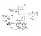
図1は、様々な実施形態による、センサシステムの一例の概略図である。本システムは、センサ100およびセンサIC102を含む。センサIC102は、DC測定回路108およびAC測定回路109を含む。DC測定回路108は、増幅器111、増幅器ゲイン抵抗112、アナログ−デジタル変換器(ADC)113、RLOAD抵抗器、RTIA抵抗器101、TIA増幅器120、および複数のスイッチ140〜144を含む。FIG. 1 is a schematic diagram of an example of a sensor system, according to various embodiments. The system includes a
明瞭さと簡潔さの目的で、センサIC102のすべての構成要素が示され、または記載されているわけではない。内部集積抵抗較正の構造および動作に関連する構成要素のみが記載されている。 Not all components of
センサのタイプに依存して、センサ100は、参照電極(RE)、対向電極(CE)、およびセンサ電極(SE)を含むことができる。例えば、参照電極は、検知動作中に検知電極に固定電位を維持するためにセンサIC102によって使用されてもよい。対向電極は、検知電極が酸化している場合には、いくつかの化学種を減少させることによって検知電極で回路を完成させる。対向電極の電位は、ガス濃度が変化するにつれて浮遊し、変化してもさしつかえない。対向電極上の電位は、センサIC102が検知電極を参照電極と同じ電位に維持するのに十分な電圧および電流を提供できる限り、重要でないかもしれない。センサ100にバイアスをかけることおよびセンサ100の測定は、複数のスイッチ140〜144の状態によって制御される。 Depending on the type of sensor, the
DC測定回路108は、センサ100に連結され、センサ100によって提供されるセンサ信号を測定するために使用される。AC測定回路109は、センサ100に連結され、センサ100のインピーダンスを測定することによってセンサ100の健全性を測定するために使用される。 The
ADC113は、増幅器111に連結され、少なくとも1つのゲイン抵抗器112を有する増幅器111の正の入力にアナログ電圧を提供する。増幅器111の出力はセンサ100の対向電極に連結され、センサ100に動作電圧を提供する。参照電極は、ゲイン抵抗器112を通して増幅器111の反転(例えば、負の)入力に連結される。センサ100の検知電極は、負荷抵抗103を通してTIA増幅器120に連結される。TIA増幅器120のゲイン抵抗器101は、RTIAの抵抗値を有する。The
RTIAおよびRLOAD抵抗101、103は、センサIC102に集積されて示されている。センサICおよび外部抵抗器を備える回路のサイズは、TIAゲインおよび負荷抵抗器101、103を集積することによって減少するとは言え、集積された抵抗器は、一般的には外部抵抗器ほど正確ではなく、センサおよびセンサICの正確な動作のために較正されるべきである。RTIA and RLOAD resistors 101, 103 are shown integrated in
図2は、様々な実施形態による、内部抵抗較正のためのセンサシステムの動作ブロック図である。図2のシステムは、抵抗値測定または較正回路と呼んでもよい。本システムは、電圧または電流励起回路200、TIA増幅器120、較正抵抗器211、センサ100、任意選択スイッチ290、AC測定回路109、RLOAD抵抗器103、RTIA抵抗器106、およびADC付き計算回路250を含む。 FIG. 2 is an operational block diagram of a sensor system for internal resistance calibration, according to various embodiments. The system of FIG. 2 may be referred to as a resistance measurement or calibration circuit. The system includes a voltage or
内部抵抗RTIAおよびRLOAD101、103を較正するために、較正電流ICALが、電圧励起回路200によって発生される励起電圧の印加によって、抵抗RCALを有する外部較正抵抗器211を通して発生される。別の実施形態では、ブロック200は電流励起回路である。内部抵抗RTIAおよびRLOAD101、103を較正する際の問題は、センサ100がセンサIC102に連結されている間、センサ100へのセンサ電流ISENSORがICALを減少させ、抵抗101、103を通るIXがICALと等しくないことである。この結果、抵抗器101、103の両端にわたる電圧を測定する際に誤差をもたらし、こうして、RTIAおよびRLOADの抵抗値を決定する際に誤差をもたらす。加えて、他のブロック(例えば、AC測定回路109)への比較的小さな(例えば、<0.1%)リーク電流ILEAKが、同様にICALを低減させる。RLOAD抵抗103の比較的小さい(例えば、0〜100オーム(Ω))値と、比較的高い(例えば、5kΩ)スイッチング抵抗のために、較正中にセンサを取り外すためのスイッチをセンサ100と直列に使用する必要はない。本発明者は、センサ100がセンサIC102に接続されたままである間に、抵抗RCALおよびRLOAD101、103を較正および測定する方法を決定した。In order to calibrate the internal resistances RTIA and
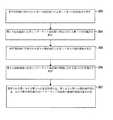
図3は、様々な実施形態による、内部集積回路抵抗較正のための方法の実施形態のフローチャートである。図3の方法を議論する際に、図2の動作ブロック図も参照する。図3の方法は、内部抵抗器101、103の抵抗を較正する際に実行されるDC測定を例示する。 FIG. 3 is a flowchart of an embodiment of a method for internal integrated circuit resistance calibration, according to various embodiments. In discussing the method of FIG. 3, reference is also made to the operational block diagram of FIG. The method of FIG. 3 illustrates a DC measurement performed in calibrating the resistance of the
ブロック303において、異なる第1および第2の励起電流(ICAL1およびICAL2)が、較正抵抗器211に印加される異なる第1および第2の励起電圧(VX1およびVX2)に応答して発生される。電圧励起回路200は、抵抗RCALを有する較正抵抗器211にわたって印加される第1および第2の励起電圧を発生する。例示だけの目的で、第1の励起電圧VX1は10mVであってもよく、第2の励起電圧VX2は20mVであってもよい。他の実施形態は、他の電圧または2つ以上の電圧を使用してもよい。さらに他の実施形態では、励起電圧を使用する代わりに、1つ以上の励起電流が較正抵抗器211を通して発生されてもよい。In
較正抵抗器211は、センサIC102の外部にある。RCALの値は、第1および第2の励起電圧によってそれぞれ発生されて較正抵抗器211を通る第1および第2のICAL電流を決定するために使用されるので、既知の抵抗値であってもよい。
較正電流ICALは、以下のように表し得る:
ICAL=IX+ISENSOR+ILEAK,
ここで、IXは、較正される1つ以上のターゲット抵抗器を流れる電流であり、ISENSORは、センサ電流であり、ILEAKは、センサICの他のブロックによって生じるリーク電流である。オームの法則を使用して、ICALのこの等式は次のように表されてもよい:
ICAL = IX + ISENSOR + ILEAK ,
Where IX is the current through one or more target resistors to be calibrated, ISENSOR is the sensor current, and ILEAK is the leakage current caused by other blocks of the sensor IC. Using Ohm's law, this equation of ICAL may be expressed as:
RXの抵抗値は、次のように表し得る:
図3のブロック305において、対応する異なる第1および第2の励起電流(IX1およびIX2)に応答して、異なる第1および第2の応答電圧(VX1およびVX2)がそれぞれターゲット抵抗器RXにわたって測定される。電圧測定は、オンチップ電圧測定回路230(例えば、ADC)によってなされ得る。電圧、電流または抵抗の測定値は、本明細書で計算を実行するための計算回路250(例えば、ADCを含む)に入力されてもよい。2つ以上の電圧を励起することにより、センサ電流とリーク電流を除去することができる:
ICAL1およびICAL2測定値を差し引くと、次のようになる:
こうして、上記から、ターゲット抵抗器(RX)の抵抗値は、図3のブロック307に示すように、測定された第1および第2の応答電圧間の差(ΔVX)、第1および第2の励起電圧間の差(ΔVexc)または1つ以上の励起電流、および較正抵抗値RCALを使用して決定されることがわかる。RXのこの値は、ターゲット抵抗器の決定された集積抵抗値を使用して、ターゲット抵抗器の集積抵抗値を調整する際に使用することができる。調整された抵抗値は、次に、センサ測定中にRLOADまたはRTIA抵抗値のいずれかとして使用することができる。Thus, from the above, the resistance value of the target resistor (RX ) is the difference between the measured first and second response voltages (ΔVX ), the first and the first, as shown in
概して、センサ電流ISENSORは、ガス濃度に関連し、RX値を決定するために複数のDC測定が行われている時間に変化しそうにない。しかしながら、別の実施形態では、AC測定を実行することによってISENSORの可能な変化を考慮に入れることができる。In general, the sensor current ISENSOR is related to the gas concentration and is unlikely to change at the time when multiple DC measurements are being taken to determine theRX value. However, in another embodiment, possible changes in ISENSOR can be taken into account by performing AC measurements.
AC測定中に、ISENSORおよびILEAK電流は特定の周波数で消滅する。特定の周波数は、センサによる経験的実験またはセンサの既知の特性によって決定されてもよい。こうして、第1および第2の励起電圧は、第1および第2の周波数を含むことができる。抵抗器RLOADおよびRTIAの両端にわたる電圧が測定される。これらの電圧は、2つの構成要素を有し、一方は励起周波数に相関し、他方はセンサ電流に相関する。しかしながら、エネルギーのスペクトルは、異なる周波数で異なる。したがって、特定の周波数での測定された電圧を抽出するために高速フーリエ変換(FFT)バンドパスフィルタを使用してもよい。既知の電圧および既知の電流を用いて、ターゲット抵抗器の抵抗値をオームの法則を用いて決定することができる。During the AC measurement, the ISENSOR and ILEAK currents disappear at a specific frequency. The particular frequency may be determined by empirical experimentation with the sensor or known characteristics of the sensor. Thus, the first and second excitation voltages can include first and second frequencies. The voltage across resistors RLOAD and RTIA is measured. These voltages have two components, one that correlates to the excitation frequency and the other that correlates to the sensor current. However, the spectrum of energy is different at different frequencies. Thus, a Fast Fourier Transform (FFT) bandpass filter may be used to extract the measured voltage at a specific frequency. Using a known voltage and a known current, the resistance value of the target resistor can be determined using Ohm's law.
上述した実施形態では、センサ100はスイッチなしでセンサインターフェースIC102に接続されている。別の実施形態では、センサ100は、任意選択のスイッチ290を通してセンサインターフェースIC102に連結されてもよい。この実施形態では、スイッチ290を開くことによって、ターゲット抵抗器抵抗を決定するための任意の測定中に、センサ100は、センサインターフェースIC102に連結された状態から取り外すことができる。 In the embodiment described above, the
図2を参照して、較正動作の間に、センサ100のCEおよびRE電極は浮いていることがわかる。センサ100は、比較的大きな容量を有するキャパシタとして働く。加算ノード電圧VSUM(例えば、電圧検知ノード)の変動は、センサ容量をセンサICに放電させ、したがって電流がISENSORとして流れることを引き起こす。前に説明したように、RLOADまたはRTIAのどちらかを較正することで引き起こされる不正確さのため、どんなISENSOR電流も望ましくない。したがって、異なる特性を有するセンサICに連結された異なるセンサのためにVSUM電圧を変化させないようにすることが望ましい。図4〜7に図示された実施形態は、異なるセンサおよびそれらのそれぞれの特性を説明するために、RLOADまたはRTIAを較正するために使用することができる。Referring to FIG. 2, it can be seen that the CE and RE electrodes of
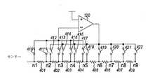
図4は、様々な実施形態による、構成可能なRLOADおよびRTIAアーキテクチャの概略図である。このアーキテクチャは、抵抗値測定および較正回路の一部である。FIG. 4 is a schematic diagram of a configurable RLOAD and RTIA architecture according to various embodiments. This architecture is part of a resistance measurement and calibration circuit.
本アーキテクチャは、複数の抵抗器401〜408(例えば、抵抗器のネットワーク)と、抵抗器のネットワークをTIA増幅器120に切り替え可能に連結するための複数のスイッチ410〜422とを含む。前述したように、RLOADまたはRTIAとセンサとの間にスイッチを配置すると、スイッチの抵抗が問題を引き起こす可能性があるが、抵抗器と増幅器120との間にスイッチを配置するとそのような問題は存在しない。スイッチ410〜422は、スイッチが閉じられるときにトランジスタが活性化され、スイッチが開いているときにトランジスタが非活性化されるようなトランジスタを用いてなどの様々な方法で実施されてもよい。The architecture includes a plurality of resistors 401-408 (eg, a resistor network) and a plurality of switches 410-422 for switchably coupling the resistor network to the
抵抗器のネットワークは2つの抵抗器のグループに分けられている。第1のグループの抵抗器は、TIA増幅器120の反転入力とセンサとの間で切り替え可能に連結可能である。第2のグループの抵抗器は、TIA増幅器120の出力とTIA増幅器120の反転入力との間で切り替え可能に連結可能である。 The resistor network is divided into two resistor groups. The first group of resistors can be switchably coupled between the inverting input of the
各隣接する抵抗器の対は、ノードN1〜N9によって共に連結される。少なくとも1つのスイッチが、それぞれのノード、および増幅器120の反転入力または増幅器120の出力の少なくとも1つに連結される。例えば、スイッチ410、411、413、415、417は、それぞれのノードと増幅器120の反転入力との間に連結される。同様に、スイッチ412、414、416、418〜422は、それぞれのノードと増幅器120の出力との間に連結される。スイッチは、計算回路250の制御出力によって制御される。 Each adjacent resistor pair is connected together by nodes N1-N9. At least one switch is coupled to each node and at least one of the inverting input of
VSUMが変化しないようにするために、VSUMノードが増幅器120の反転入力に直接接続されるようにRLOADはゼロオームの抵抗に設定される。しかしながら、RLOADをゼロオームに設定する前に、RLOADとRTIAとの間の適切な比が確立されるように、RTIAがまず決定されるべきである。ICAL電流信号をVX電圧信号に正確に変換するには、正確なRTIAが必要である。これは、第1の抵抗構成要素RLOADの抵抗値を第2の抵抗構成要素RTIAの抵抗値に関連して変化させるために、RLOADおよびRTIA抵抗値を下記のように変更するようにスイッチを設定することによって達成される。To prevent VSUM from changing, RLOAD is set to a zero ohm resistance so that the VSUM node is connected directly to the inverting input of
図5は、様々な実施形態による、公称動作モードの初期構成例における構成可能なRLOADおよびRTIAアーキテクチャの概略図である。図5の構成は、スイッチ413を閉じて、ノードN1とノードN3との間の抵抗401および402を増幅器120の反転入力に接続することによって、RLOADがいくらかの初期抵抗に設定される構成例である。こうして、RLOADは、今やこれらの2つの抵抗器401、402の合計である。RTIAは、ノードN3とノードN7との間の抵抗器の合計がRTIAに対する抵抗となるようにスイッチ420を閉じることによって設定される。RLOADおよびRTIAの初期抵抗値は、センサ特性およびRLOADおよびRTIAに対するセンサの要件に基づいて決定される。FIG. 5 is a schematic diagram of a configurable RLOAD and RTIA architecture in an initial configuration example of a nominal mode of operation, according to various embodiments. The configuration of FIG. 5 is a configuration example in which RLOAD is set to some initial resistance by closing
図6は、様々な実施形態による、図5の実施形態からRLOADを測定する別の構成例における構成可能なRLOADおよびRTIAアーキテクチャの概略図である。この構成は、TIA増幅器120の反転入力がVSUMノードに直接接続されるように、RLOADをバイパスする(例えば、ゼロオームに設定される)。こうして、RTIAはRLOADの以前の抵抗値と同じになる。これはスイッチ410を閉じて増幅器の反転入力をVSUMノードに直接接続し、スイッチ414を閉じてノードN1とN3の間の抵抗器401と402をRLOADの以前の抵抗値であるRTIAとして接続することによって達成される。新しいRTIA抵抗は、TIA増幅器120の出力と反転入力との間にあるので、元のRLOAD抵抗値は、新しいRTIAの両端にわたる差電圧を測定することによって測定することができる。この電圧差は、上述の式のVXである。VexcおよびRCALは既知であるので、抵抗RX(RLOAD)を今や計算できる。この抵抗は一時的にRTEMP1として設定される。FIG. 6 is a schematic diagram of a configurable RLOAD and RTIA architecture in another example configuration for measuring RLOAD from the embodiment of FIG. 5, according to various embodiments. This configuration bypasses RLOAD (eg, set to zero ohms) so that the inverting input of
図7は、様々な実施形態による、図5のRLOAD+RTIAを測定する別の構成例における構成可能なRLOADおよびRTIAアーキテクチャの概略図である。RTIAは、初期RLOAD+初期RTIAの合計抵抗として今や設定できる。これは、RTEMP2=RLOAD+RTIAで表してもよい。これは、VSUMノードを増幅器120の反転入力に直接接続するためにスイッチ410を閉じることによりRLOADをバイパスすることによって、図7に図示するように達成され、こうしてRLOADゼロオームにする。RTIAが増幅器120の出力に接続され、ノードN1とノードN7との間の抵抗401〜406のすべての合計となるように、スイッチ420が閉じられる。今やRTEMP2の合計抵抗を測定するための測定を実行することができる。FIG. 7 is a schematic diagram of a configurable RLOAD and RTIA architecture in another example configuration for measuring RLOAD + RTIA of FIG. 5, according to various embodiments. RTIA can now be set as the total resistance of initial RLOAD + initial RTIA . This may be expressed as RTEMP2 = RLOAD + RTIA . This is accomplished as illustrated in FIG. 7 by bypassing RLOAD by closing switch 410 to connect the VSUM node directly to the inverting input of
こうして、RTIAは、式からRLOADを除去するためにRTEMP2からRTEMP1を差し引くことによって決定することができる。これは、RTIAの決定をもたらす。言い換えれば、RTIA=RTEMP2−RTEMP1である。Thus, RTIA can be determined by subtracting RTEMP1 from RTEMP2 to remove RLOAD from the equation. This leads to the determination of RTIA . In other words, RTIA = RTEMP2 −RTEMP1 .
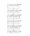
図8は、様々な実施形態による、内部集積回路抵抗較正のための方法の実施形態のフローチャートである。ブロック801において、RLOADおよびRTIAは、センサ特性によって決定される初期値に設定される。ブロック803において、RLOADは、ゼロオームに設定されるようにバイパスされ、それにより、新しいRTIAが初期RLOADに設定される。ブロック805において、VXがRTIAにわたって測定され、既知のVexcおよびRCALに基づいて、RTEMP1を、上記のRx式
上記の詳細な説明は、詳細な説明の一部を構成する添付の図面への参照を含む。図面は、例示として、本発明を実施することができる特定の実施形態を示す。これらの実施形態は、本明細書では「例」とも呼ばれる。本文書で言及されるすべての刊行物、特許および特許文書は、参照により個々に組み込まれているように、その全体が参照により本明細書に組み込まれる。この文書と参照により組み込まれているそれらの文書との間に矛盾する使用があった場合、組み込まれた参考文献の使用はこの文書の補足とみなされるべきであり、両立しない矛盾については、この文書の使用方法が統制する。 The above detailed description includes references to the accompanying drawings, which form a part of the detailed description. The drawings show, by way of illustration, specific embodiments in which the invention can be practiced. These embodiments are also referred to herein as “examples”. All publications, patents and patent documents mentioned in this document are hereby incorporated by reference in their entirety, as if individually incorporated by reference. If there is a conflicting use between this document and those documents incorporated by reference, the use of the incorporated reference should be considered a supplement to this document, and The use of documents is controlled.
本文書では、用語「1つの(a)」または「1つの(an)」は、特許文書において一般的であるように、「少なくとも1つ」または「1つ以上」の他の事例または用途とは無関係に、1つまたは1つ以上を含むように使用される。本明細書において、「または(or)」という用語は、特に指示しない限り、「AまたはB」は「BでなくA」、「AでなくB」、および「AかつB」を含むように、非排他的論理和に言及するために使用される。添付の特許請求の範囲において、用語「含む(including)」および「その中で(in which)」は、それぞれの用語「備える(comprising)」および「ここで(wherein)」の平易な英語の等価物として使用される。また、以下の特許請求の範囲において、「含む(including)」および「備える(comprising)」という用語は、拡張可能であり、すなわち、請求項におけるそのような用語の後に列挙された要素に加えて要素を含むシステム、装置、物品、またはプロセスが、依然としてその請求の範囲内にあるとみなされる。さらに、以下の特許請求の範囲において、「第1の」、「第2の」および「第3の」などの用語は単にラベルとして使用され、それらの対象に数値的な要件を課すことを意図しない。本明細書に記載の方法の例は、少なくとも部分的に機械的にまたはコンピュータで実施することができる。 In this document, the term “a” or “an” refers to other instances or uses of “at least one” or “one or more”, as is common in patent documents. Are used independently to include one or more. In this specification, the term “or”, unless otherwise indicated, “A or B” includes “A not B”, “B not A”, and “A and B”. Used to refer to non-exclusive OR. In the appended claims, the terms “including” and “in which” refer to the plain English equivalent of the terms “comprising” and “where”, respectively. Used as a thing. Also, in the following claims, the terms “including” and “comprising” are extensible, that is, in addition to the elements listed after such terms in the claims. Systems, devices, articles, or processes that include the elements are still considered to be within the scope of the claims. Further, in the following claims, terms such as “first”, “second” and “third” are merely used as labels and are intended to impose numerical requirements on their subject matter. do not do. The example methods described herein can be at least partially mechanically or computer-implemented.
上記の説明は例示的なものであり、限定的なものではない。例えば、上記の例(またはその1つ以上の態様)は、互いに組み合わせて使用されてもよい。当業者が上記の説明を検討することによって、他の実施形態を使用することができる。読者が技術的開示の性質を迅速に確認できるように要約が提供されている。それは、請求項の範囲または意味を解釈または制限するために使用されるものではないという理解の下で提出されている。また、上記の詳細な説明において、開示を合理化するために様々な特徴をグループ化してもよい。これは、請求されていない開示された特徴がいずれかの請求項に不可欠であることを意図していると解釈されるべきではない。むしろ、発明の主題は、特定の開示された実施形態のすべての特徴よりも少なくてもよい。したがって、以下の請求項は、発明の詳細な説明に組み込まれており、各請求項は別個の実施形態として独自の立場をとる。本発明の範囲は、そのような特許請求の範囲が権利を与えられる等価物の全範囲とともに、添付の特許請求の範囲を参照して決定されるべきである。 The above description is illustrative and not restrictive. For example, the above examples (or one or more aspects thereof) may be used in combination with each other. Other embodiments can be used by one of ordinary skill in the art upon reviewing the above description. A summary is provided so that the reader can quickly ascertain the nature of the technical disclosure. It is submitted with the understanding that it will not be used to interpret or limit the scope or meaning of the claims. In the above detailed description, various features may be grouped in order to streamline the disclosure. This should not be interpreted as intending that an unclaimed disclosed feature is essential to any claim. Rather, the subject matter of the invention may be less than all the features of a particular disclosed embodiment. Thus, the following claims are hereby incorporated into the Detailed Description, with each claim standing on its own as a separate embodiment. The scope of the invention should be determined with reference to the appended claims, along with the full scope of equivalents to which such claims are entitled.
100 センサ
101 抵抗器
103 抵抗器
106 抵抗器
108 測定回路
109 AC測定回路
111 増幅器
112 ゲイン抵抗器
113 アナログ−デジタル変換器(ADC)
120 増幅器
140、141、142、143、144 スイッチ
200 電圧または電流励起回路
211 較正抵抗器
230 電圧測定回路
250 計算回路
290 スイッチ
401〜408 抵抗器
410〜422 スイッチDESCRIPTION OF
120
Claims (20)
Translated fromJapanese指定された較正抵抗値を有する較正抵抗器に印加される異なる第1および第2の指定された励起電圧に応答して、異なる第1および第2の励起電流を発生することと、
前記対応する異なる第1および第2の励起電流にそれぞれ応答して、前記ターゲット抵抗器の両端にわたる異なる第1および第2の応答電圧を測定することと、
前記測定された第1および第2の応答電圧間の差、前記第1および第2の指定された励起電圧間の差、および前記指定された較正抵抗値を使用して、前記ターゲット抵抗器の前記集積回路抵抗値を決定することと、を含む、方法。A method of measuring an integrated circuit (IC) resistance value of the target resistor using an excitation current to be reduced by a leakage current of an external sensor or other leakage current before reaching the target resistor,
Generating different first and second excitation currents in response to different first and second specified excitation voltages applied to a calibration resistor having a specified calibration resistance value;
Measuring different first and second response voltages across the target resistor in response to the corresponding different first and second excitation currents, respectively;
Using the difference between the measured first and second response voltages, the difference between the first and second designated excitation voltages, and the designated calibration resistance value, Determining the integrated circuit resistance value.
前記センサによって生成された応答電流を検知するための少なくとも1つのターゲット抵抗器を含む、電流センサ回路と、
前記ターゲット抵抗器の抵抗値を測定するために前記ターゲット抵抗器に連結された抵抗値測定回路であって、
指定された較正抵抗値を有する較正抵抗器に1つ以上の指定された励起電圧を印加し、それに応答して、各指定された励起電圧に対する異なるそれぞれの励起電流を発生するする電圧励起回路と、
各対応する異なる励起電流に応答して、それぞれ前記ターゲット抵抗器の両端にわたる異なるそれぞれの応答電圧を測定する電圧測定回路と、
前記測定された異なるそれぞれの応答電圧間の差、前記1つ以上の指定された励起電圧間の差、および前記指定された較正抵抗値、を使用して、前記ターゲット抵抗器の前記抵抗値を決定する計算回路と、を含む、抵抗値測定回路と、を含む、センサインターフェース集積回路。A sensor interface integrated circuit (IC) for measuring a resistance value of a target resistor using an excitation current to be reduced by an external sensor leakage current of a sensor connected to a sensor interface IC,
Comprising at least one target resistor for detecting aresponse current generated by the sensor, a current sensor circuit,
A resistance value measurement circuit connected to the target resistor for measuring a resistance value of the target resistor,
A voltage excitation circuit that applies one or more specified excitation voltages to a calibration resistor having a specified calibration resistance value, and in response generates a different respective excitation current for each specified excitation voltage; ,
A voltage measurement circuit that measures different respective response voltages across the respective target resistors in response to each corresponding different excitation current;
Using the difference between the measured different respective response voltages, the difference between the one or more specified excitation voltages, and the specified calibration resistance value, the resistance value of the target resistor is calculated. A sensor interface integrated circuit including a resistance value measuring circuit including a calculation circuit for determining.
前記センサによって生成された応答電流を検知するための少なくとも1つのターゲット抵抗器を含む電流センサ回路と、
前記ターゲット抵抗器に連結され、前記ターゲット抵抗器の抵抗値を測定または較正する抵抗値測定または較正回路であって、
指定された較正抵抗値を有する較正抵抗器を通して1つ以上の指定された励起電流を印加する電流励起回路と、
各対応する異なる励起電流に応答して、それぞれ前記ターゲット抵抗器の両端にわたる異なるそれぞれの応答電圧を測定する電圧測定回路と、
前記測定された異なるそれぞれの応答電圧間の差、前記1つ以上の指定された励起電流間の差、および前記指定された較正抵抗値を使用して、前記ターゲット抵抗器の前記抵抗値を決定する計算回路と、を含む、抵抗値測定または較正回路と、を含む、センサインターフェース集積回路(IC)。A sensor interface integrated circuit (IC) for measuring or calibrating a resistance value of a target resistor using an excitation current to be reduced by an external sensor leakage current of a sensor connected to the IC,
A current sensor circuit including at least one target resistor for detecting aresponse current generated by said sensor,
A resistance value measurement or calibration circuit coupled to the target resistor and measuring or calibrating a resistance value of the target resistor;
A current excitation circuit that applies one or more specified excitation currents through a calibration resistor having a specified calibration resistance value;
A voltage measurement circuit that measures different respective response voltages across the respective target resistors in response to each corresponding different excitation current;
Using the difference between the different measured response voltages measured, the difference between the one or more specified excitation currents, and the specified calibration resistance value, the resistance value of the target resistor is determined. A sensor interface integrated circuit (IC) including a resistance measurement or calibration circuit including a calculation circuit.
前記増幅器の反転入力と前記センサとの間で切り替え可能に連結可能な第1のグループの抵抗器と、
前記増幅器の出力と前記反転入力との間で切り替え可能に連結可能な第2のグループの抵抗器と、を備える、請求項17に記載のセンサインターフェースIC。The resistor network is:
A first group of resistors switchably connectable between an inverting input of the amplifier and the sensor;
18. A sensor interface IC according to claim 17, comprising a second group of resistors switchably connectable between the output of the amplifier and the inverting input.
Applications Claiming Priority (2)
| Application Number | Priority Date | Filing Date | Title |
|---|---|---|---|
| US15/586,877US10429483B2 (en) | 2017-05-04 | 2017-05-04 | Internal integrated circuit resistance calibration |
| US15/586,877 | 2017-05-04 |
Publications (2)
| Publication Number | Publication Date |
|---|---|
| JP2018190979A JP2018190979A (en) | 2018-11-29 |
| JP6619471B2true JP6619471B2 (en) | 2019-12-11 |
Family
ID=64014132
Family Applications (1)
| Application Number | Title | Priority Date | Filing Date |
|---|---|---|---|
| JP2018088746AActiveJP6619471B2 (en) | 2017-05-04 | 2018-05-02 | Calibration of internal integrated circuit resistance |
Country Status (5)
| Country | Link |
|---|---|
| US (1) | US10429483B2 (en) |
| JP (1) | JP6619471B2 (en) |
| CN (1) | CN108802495B (en) |
| DE (1) | DE102018110578B4 (en) |
| TW (1) | TWI670490B (en) |
Families Citing this family (12)
| Publication number | Priority date | Publication date | Assignee | Title |
|---|---|---|---|---|
| EP3722796B1 (en)* | 2019-04-10 | 2022-08-03 | Carrier Corporation | Integrated, miniaturized, wireless sensing electronic platform for high resolution gas sensing |
| US11656193B2 (en) | 2020-06-12 | 2023-05-23 | Analog Devices, Inc. | Self-calibrating polymer nano composite (PNC) sensing element |
| TWI738387B (en)* | 2020-06-18 | 2021-09-01 | 台灣積體電路製造股份有限公司 | Method, system and apparatus for measuring resistance of semiconductor device |
| JP2022047708A (en)* | 2020-09-14 | 2022-03-25 | 北斗電工株式会社 | Gas detector |
| US11499995B2 (en) | 2020-10-26 | 2022-11-15 | Analog Devices, Inc. | Leakage compensation technique for current sensor |
| CN116324431A (en) | 2020-10-27 | 2023-06-23 | 美国亚德诺半导体公司 | Wireless Integrity Sensing Acquisition Module |
| CN114689922A (en)* | 2020-12-31 | 2022-07-01 | 金卡智能集团股份有限公司 | Current detection circuit and gas meter |
| DE102021130852B3 (en)* | 2021-11-24 | 2023-02-16 | Elmos Semiconductor Se | Identification of the wetting of NTC temperature measurement resistors in safety-related devices |
| CN114485764B (en)* | 2022-02-16 | 2023-08-01 | 中国核动力研究设计院 | Self-calibration and anti-drift device for weak signal measurement |
| US11609593B1 (en)* | 2022-04-02 | 2023-03-21 | Oleksandr Kokorin | Fast LCR meter with leakage compensation |
| WO2023202889A1 (en)* | 2022-04-19 | 2023-10-26 | ams Sensors Germany GmbH | Bioelectrical impedance analysis circuit, test system, analysis system and method of determining a bioelectrical impedance |
| CN119534553B (en)* | 2025-01-23 | 2025-04-08 | 成都晶宝时频技术股份有限公司 | Analysis method for liquid phase measurement of electrodeless quartz crystal |
Family Cites Families (23)
| Publication number | Priority date | Publication date | Assignee | Title |
|---|---|---|---|---|
| DE288215T1 (en) | 1987-04-24 | 1989-03-09 | Simmonds Precision Products, Inc., Tarrytown, N.Y. | DETERMINATION OF ELECTRICAL CAPACITY AND ELECTRICAL RESISTANCE. |
| JPH0738844Y2 (en)* | 1988-10-07 | 1995-09-06 | トヨタ自動車株式会社 | Heater controller for oxygen sensor |
| JPH07159460A (en)* | 1993-12-07 | 1995-06-23 | Toshiba Corp | Resistance sensor input device |
| US6452405B1 (en) | 1999-09-17 | 2002-09-17 | Delphi Technologies, Inc. | Method and apparatus for calibrating a current sensing system |
| US6695475B2 (en) | 2001-05-31 | 2004-02-24 | Stmicroelectronics, Inc. | Temperature sensing circuit and method |
| KR100497991B1 (en) | 2002-07-29 | 2005-07-01 | 세주엔지니어링주식회사 | Portable gas detector and re-calibration method thereof |
| JP4071157B2 (en)* | 2003-05-27 | 2008-04-02 | セイコーインスツル株式会社 | Image sensor |
| JP2010145373A (en)* | 2008-12-22 | 2010-07-01 | Espec Corp | Resistance measuring apparatus |
| US8337082B2 (en)* | 2009-05-08 | 2012-12-25 | Canon U.S. Life Sciences, Inc. | Systems and methods for auto-calibration of resistive temperature sensors |
| JP5482221B2 (en)* | 2010-01-22 | 2014-05-07 | 株式会社リコー | Analog circuit |
| WO2011151856A1 (en)* | 2010-05-31 | 2011-12-08 | 株式会社アドバンテスト | Measurement device and measurement method |
| US8714816B2 (en) | 2010-09-12 | 2014-05-06 | Medisim Ltd. | Temperature sensor with calibrated analog resistive output |
| CN102353825B (en)* | 2011-06-03 | 2014-02-19 | 清华大学 | A resistance sampling isolation current detection circuit |
| US9086442B2 (en)* | 2012-05-07 | 2015-07-21 | Bristol, Inc. | Methods and apparatus to detect leakage current in a resistance temperature detector |
| JP6142003B2 (en)* | 2014-01-08 | 2017-06-07 | 旭化成エレクトロニクス株式会社 | Diode type sensor output current detection IC chip and diode type sensor device |
| US9720020B2 (en)* | 2014-05-28 | 2017-08-01 | Nxp B.V. | Broad-range current measurement using variable resistance |
| FR3024920A1 (en)* | 2014-08-13 | 2016-02-19 | St Microelectronics Grenoble 2 | INTEGRATED CIRCUIT CHIP WITH DERIVED CORRECTED TEMPERATURE |
| JP2016090379A (en)* | 2014-11-05 | 2016-05-23 | セイコーエプソン株式会社 | measuring device |
| JP6416601B2 (en)* | 2014-11-28 | 2018-10-31 | 株式会社アドバンテスト | measuring device |
| DE102015203866A1 (en)* | 2015-03-04 | 2016-09-08 | Fraunhofer-Gesellschaft zur Förderung der angewandten Forschung e.V. | Method and device for leakage-current compensated resistance measurement |
| DE102015105075A1 (en)* | 2015-04-01 | 2016-10-06 | Infineon Technologies Ag | current sensor |
| KR102451873B1 (en)* | 2016-12-13 | 2022-10-06 | 현대자동차 주식회사 | APPARATUS FOR resistance measurement |
| US10495566B2 (en)* | 2017-03-30 | 2019-12-03 | Dell Products L.P. | Circuits, systems and methods for corrosion detection |
- 2017
- 2017-05-04USUS15/586,877patent/US10429483B2/enactiveActive
- 2018
- 2018-05-02JPJP2018088746Apatent/JP6619471B2/enactiveActive
- 2018-05-03DEDE102018110578.9Apatent/DE102018110578B4/enactiveActive
- 2018-05-04TWTW107115264Apatent/TWI670490B/enactive
- 2018-05-04CNCN201810419461.0Apatent/CN108802495B/enactiveActive
Also Published As
| Publication number | Publication date |
|---|---|
| US20180321349A1 (en) | 2018-11-08 |
| US10429483B2 (en) | 2019-10-01 |
| JP2018190979A (en) | 2018-11-29 |
| CN108802495B (en) | 2020-11-20 |
| DE102018110578B4 (en) | 2021-03-04 |
| CN108802495A (en) | 2018-11-13 |
| TWI670490B (en) | 2019-09-01 |
| DE102018110578A1 (en) | 2018-11-29 |
| TW201903401A (en) | 2019-01-16 |
Similar Documents
| Publication | Publication Date | Title |
|---|---|---|
| JP6619471B2 (en) | Calibration of internal integrated circuit resistance | |
| JP7390976B2 (en) | Devices and methods for smart sensor applications | |
| US10288674B2 (en) | Impedance characteristic circuit for electrochemical sensor | |
| US8508217B2 (en) | Output circuit of charge mode sensor | |
| US20070103174A1 (en) | Direct current test apparatus | |
| JP2018189651A5 (en) | ||
| US10591429B2 (en) | Control circuit for use with a four terminal sensor, and measurement system including such a control circuit | |
| US9726705B2 (en) | Sensor interface circuits | |
| US9859878B2 (en) | Control circuit for use with a sensor, and measurement system including such a control circuit | |
| Matute et al. | Characterization of drift and hysteresis errors in force sensing resistors considering their piezocapacitive effect | |
| US8896292B2 (en) | System and method for gain adjustment in transimpedance amplifier configurations for analyte measurement | |
| JP6718284B2 (en) | Signal processing circuit, coulomb counter circuit, electronic device | |
| US20190128747A1 (en) | Sensor apparatus | |
| CN209627352U (en) | A kind of pressure sensitivity push button signalling detection circuit and electronic equipment | |
| JP3393203B2 (en) | Inspection method of current detection circuit | |
| JP3562703B2 (en) | Measuring device | |
| CN101918851A (en) | Voltage source measurement unit with minimized common mode errors | |
| CN108168724B (en) | Novel NTC temperature detection method and system | |
| EP3629477B1 (en) | Circuit arrangement and sensor arrangements including the same | |
| CN116087824A (en) | Leakage and Load Detection Circuitry | |
| RU2405131C1 (en) | Temperature difference metre with thermistor transducers | |
| CN116400283A (en) | Resistor self-correction circuit and correction method |
Legal Events
| Date | Code | Title | Description |
|---|---|---|---|
| A621 | Written request for application examination | Free format text:JAPANESE INTERMEDIATE CODE: A621 Effective date:20180717 | |
| A977 | Report on retrieval | Free format text:JAPANESE INTERMEDIATE CODE: A971007 Effective date:20190418 | |
| A131 | Notification of reasons for refusal | Free format text:JAPANESE INTERMEDIATE CODE: A131 Effective date:20190513 | |
| A521 | Request for written amendment filed | Free format text:JAPANESE INTERMEDIATE CODE: A523 Effective date:20190809 | |
| TRDD | Decision of grant or rejection written | ||
| A01 | Written decision to grant a patent or to grant a registration (utility model) | Free format text:JAPANESE INTERMEDIATE CODE: A01 Effective date:20191021 | |
| A61 | First payment of annual fees (during grant procedure) | Free format text:JAPANESE INTERMEDIATE CODE: A61 Effective date:20191114 | |
| R150 | Certificate of patent or registration of utility model | Ref document number:6619471 Country of ref document:JP Free format text:JAPANESE INTERMEDIATE CODE: R150 | |
| R250 | Receipt of annual fees | Free format text:JAPANESE INTERMEDIATE CODE: R250 | |
| R250 | Receipt of annual fees | Free format text:JAPANESE INTERMEDIATE CODE: R250 | |
| R250 | Receipt of annual fees | Free format text:JAPANESE INTERMEDIATE CODE: R250 |