JP6602585B2 - Display device and electronic device - Google Patents
Display device and electronic deviceDownload PDFInfo
- Publication number
- JP6602585B2 JP6602585B2JP2015148420AJP2015148420AJP6602585B2JP 6602585 B2JP6602585 B2JP 6602585B2JP 2015148420 AJP2015148420 AJP 2015148420AJP 2015148420 AJP2015148420 AJP 2015148420AJP 6602585 B2JP6602585 B2JP 6602585B2
- Authority
- JP
- Japan
- Prior art keywords
- region
- display
- display panel
- layer
- substrate
- Prior art date
- Legal status (The legal status is an assumption and is not a legal conclusion. Google has not performed a legal analysis and makes no representation as to the accuracy of the status listed.)
- Active
Links
Images


Classifications
- H—ELECTRICITY
- H05—ELECTRIC TECHNIQUES NOT OTHERWISE PROVIDED FOR
- H05B—ELECTRIC HEATING; ELECTRIC LIGHT SOURCES NOT OTHERWISE PROVIDED FOR; CIRCUIT ARRANGEMENTS FOR ELECTRIC LIGHT SOURCES, IN GENERAL
- H05B33/00—Electroluminescent light sources
- H05B33/12—Light sources with substantially two-dimensional radiating surfaces
- G—PHYSICS
- G06—COMPUTING OR CALCULATING; COUNTING
- G06F—ELECTRIC DIGITAL DATA PROCESSING
- G06F1/00—Details not covered by groups G06F3/00 - G06F13/00 and G06F21/00
- G06F1/16—Constructional details or arrangements
- G06F1/1613—Constructional details or arrangements for portable computers
- G06F1/1633—Constructional details or arrangements of portable computers not specific to the type of enclosures covered by groups G06F1/1615 - G06F1/1626
- G06F1/1637—Details related to the display arrangement, including those related to the mounting of the display in the housing
- G06F1/1652—Details related to the display arrangement, including those related to the mounting of the display in the housing the display being flexible, e.g. mimicking a sheet of paper, or rollable
- H—ELECTRICITY
- H05—ELECTRIC TECHNIQUES NOT OTHERWISE PROVIDED FOR
- H05B—ELECTRIC HEATING; ELECTRIC LIGHT SOURCES NOT OTHERWISE PROVIDED FOR; CIRCUIT ARRANGEMENTS FOR ELECTRIC LIGHT SOURCES, IN GENERAL
- H05B33/00—Electroluminescent light sources
- H05B33/02—Details
- H—ELECTRICITY
- H10—SEMICONDUCTOR DEVICES; ELECTRIC SOLID-STATE DEVICES NOT OTHERWISE PROVIDED FOR
- H10K—ORGANIC ELECTRIC SOLID-STATE DEVICES
- H10K59/00—Integrated devices, or assemblies of multiple devices, comprising at least one organic light-emitting element covered by group H10K50/00
- H10K59/10—OLED displays
- H10K59/18—Tiled displays
- H—ELECTRICITY
- H10—SEMICONDUCTOR DEVICES; ELECTRIC SOLID-STATE DEVICES NOT OTHERWISE PROVIDED FOR
- H10K—ORGANIC ELECTRIC SOLID-STATE DEVICES
- H10K59/00—Integrated devices, or assemblies of multiple devices, comprising at least one organic light-emitting element covered by group H10K50/00
- H10K59/40—OLEDs integrated with touch screens
- H—ELECTRICITY
- H10—SEMICONDUCTOR DEVICES; ELECTRIC SOLID-STATE DEVICES NOT OTHERWISE PROVIDED FOR
- H10K—ORGANIC ELECTRIC SOLID-STATE DEVICES
- H10K2102/00—Constructional details relating to the organic devices covered by this subclass
- H10K2102/301—Details of OLEDs
- H10K2102/311—Flexible OLED
- H—ELECTRICITY
- H10—SEMICONDUCTOR DEVICES; ELECTRIC SOLID-STATE DEVICES NOT OTHERWISE PROVIDED FOR
- H10K—ORGANIC ELECTRIC SOLID-STATE DEVICES
- H10K50/00—Organic light-emitting devices
- H10K50/80—Constructional details
- H10K50/84—Passivation; Containers; Encapsulations
- H10K50/841—Self-supporting sealing arrangements
- H—ELECTRICITY
- H10—SEMICONDUCTOR DEVICES; ELECTRIC SOLID-STATE DEVICES NOT OTHERWISE PROVIDED FOR
- H10K—ORGANIC ELECTRIC SOLID-STATE DEVICES
- H10K50/00—Organic light-emitting devices
- H10K50/80—Constructional details
- H10K50/84—Passivation; Containers; Encapsulations
- H10K50/842—Containers
- H10K50/8426—Peripheral sealing arrangements, e.g. adhesives, sealants
- H—ELECTRICITY
- H10—SEMICONDUCTOR DEVICES; ELECTRIC SOLID-STATE DEVICES NOT OTHERWISE PROVIDED FOR
- H10K—ORGANIC ELECTRIC SOLID-STATE DEVICES
- H10K50/00—Organic light-emitting devices
- H10K50/80—Constructional details
- H10K50/84—Passivation; Containers; Encapsulations
- H10K50/842—Containers
- H10K50/8428—Vertical spacers, e.g. arranged between the sealing arrangement and the OLED
- H—ELECTRICITY
- H10—SEMICONDUCTOR DEVICES; ELECTRIC SOLID-STATE DEVICES NOT OTHERWISE PROVIDED FOR
- H10K—ORGANIC ELECTRIC SOLID-STATE DEVICES
- H10K50/00—Organic light-emitting devices
- H10K50/80—Constructional details
- H10K50/84—Passivation; Containers; Encapsulations
- H10K50/844—Encapsulations
- H—ELECTRICITY
- H10—SEMICONDUCTOR DEVICES; ELECTRIC SOLID-STATE DEVICES NOT OTHERWISE PROVIDED FOR
- H10K—ORGANIC ELECTRIC SOLID-STATE DEVICES
- H10K59/00—Integrated devices, or assemblies of multiple devices, comprising at least one organic light-emitting element covered by group H10K50/00
- H10K59/10—OLED displays
- H10K59/12—Active-matrix OLED [AMOLED] displays
- H10K59/131—Interconnections, e.g. wiring lines or terminals
- H—ELECTRICITY
- H10—SEMICONDUCTOR DEVICES; ELECTRIC SOLID-STATE DEVICES NOT OTHERWISE PROVIDED FOR
- H10K—ORGANIC ELECTRIC SOLID-STATE DEVICES
- H10K59/00—Integrated devices, or assemblies of multiple devices, comprising at least one organic light-emitting element covered by group H10K50/00
- H10K59/80—Constructional details
- H10K59/87—Passivation; Containers; Encapsulations
- H10K59/871—Self-supporting sealing arrangements
- H10K59/8722—Peripheral sealing arrangements, e.g. adhesives, sealants
- H—ELECTRICITY
- H10—SEMICONDUCTOR DEVICES; ELECTRIC SOLID-STATE DEVICES NOT OTHERWISE PROVIDED FOR
- H10K—ORGANIC ELECTRIC SOLID-STATE DEVICES
- H10K59/00—Integrated devices, or assemblies of multiple devices, comprising at least one organic light-emitting element covered by group H10K50/00
- H10K59/80—Constructional details
- H10K59/87—Passivation; Containers; Encapsulations
- H10K59/871—Self-supporting sealing arrangements
- H10K59/8723—Vertical spacers, e.g. arranged between the sealing arrangement and the OLED
- H—ELECTRICITY
- H10—SEMICONDUCTOR DEVICES; ELECTRIC SOLID-STATE DEVICES NOT OTHERWISE PROVIDED FOR
- H10K—ORGANIC ELECTRIC SOLID-STATE DEVICES
- H10K59/00—Integrated devices, or assemblies of multiple devices, comprising at least one organic light-emitting element covered by group H10K50/00
- H10K59/80—Constructional details
- H10K59/87—Passivation; Containers; Encapsulations
- H10K59/873—Encapsulations
Landscapes
- Engineering & Computer Science (AREA)
- Computer Hardware Design (AREA)
- Theoretical Computer Science (AREA)
- Human Computer Interaction (AREA)
- Physics & Mathematics (AREA)
- General Engineering & Computer Science (AREA)
- General Physics & Mathematics (AREA)
- Devices For Indicating Variable Information By Combining Individual Elements (AREA)
- Electroluminescent Light Sources (AREA)
- Liquid Crystal (AREA)
- Electrochromic Elements, Electrophoresis, Or Variable Reflection Or Absorption Elements (AREA)
Description
Translated fromJapanese本発明の一態様は、表示装置に関する。 One embodiment of the present invention relates to a display device.
なお本発明の一態様は、上記の技術分野に限定されない。本明細書等で開示する発明の一態様の技術分野は、物、方法、または、製造方法に関するものである。または、本発明の一態様は、プロセス、マシン、マニュファクチャ、または、組成物(コンポジション・オブ・マター)に関するものである。そのため、より具体的に本明細書で開示する本発明の一態様の技術分野としては、半導体装置、表示装置、発光装置、照明装置、蓄電装置、記憶装置、それらの駆動方法、または、それらの製造方法、を一例として挙げることができる。 Note that one embodiment of the present invention is not limited to the above technical field. The technical field of one embodiment of the invention disclosed in this specification and the like relates to an object, a method, or a manufacturing method. Alternatively, one embodiment of the present invention relates to a process, a machine, a manufacture, or a composition (composition of matter). Therefore, the technical field of one embodiment of the present invention disclosed in this specification more specifically includes a semiconductor device, a display device, a light-emitting device, a lighting device, a power storage device, a memory device, a driving method thereof, or a driving method thereof. A manufacturing method can be mentioned as an example.
近年、表示装置の大型化が求められている。例えば、家庭用のテレビジョン装置(テレビ、またはテレビジョン受信機ともいう)、デジタルサイネージ(Digital Signage:電子看板)や、PID(Public Information Display)などが挙げられる。デジタルサイネージや、PIDなどは、大型であるほど提供できる情報量を増やすことができ、また広告等に用いる場合には大型であるほど人の目につきやすく、広告の宣伝効果を高めることが期待される。 In recent years, an increase in the size of a display device has been demanded. For example, a home television device (also referred to as a television or a television receiver), a digital signage (Digital Signage), a PID (Public Information Display), and the like can be given. For digital signage, PID, etc., the larger the size, the greater the amount of information that can be provided, and when used for advertising, etc. The
表示装置としては、代表的には有機EL(Electro Luminescence)素子や発光ダイオード(LED:Light Emitting Diode)等の発光素子を備える発光装置、液晶表示装置、電気泳動方式などにより表示を行う電子ペーパーなどが挙げられる。 As a display device, typically, a light-emitting device including a light-emitting element such as an organic EL (Electro Luminescence) element or a light-emitting diode (LED), a liquid crystal display device, an electronic paper that performs display by an electrophoresis method, or the like Is mentioned.
例えば、有機EL素子の基本的な構成は、一対の電極間に発光性の有機化合物を含む層を挟持したものである。この素子に電圧を印加することにより、発光性の有機化合物から発光を得ることができる。このような有機EL素子が適用された表示装置は、液晶表示装置等で必要であったバックライトが不要なため、薄型、軽量、高コントラストで且つ低消費電力な表示装置を実現できる。例えば、有機EL素子を用いた表示装置の一例が、特許文献1に開示されている。 For example, the basic configuration of the organic EL element is such that a layer containing a light-emitting organic compound is sandwiched between a pair of electrodes. Light emission can be obtained from the light-emitting organic compound by applying a voltage to this element. Since a display device to which such an organic EL element is applied does not require a backlight that is necessary for a liquid crystal display device or the like, a thin, lightweight, high-contrast display device with low power consumption can be realized. For example,
また、特許文献2には、フィルム基板上に、スイッチング素子であるトランジスタや有機EL素子を備えたフレキシブルなアクティブマトリクス型の発光装置が開示されている。
本発明の一態様は、大型化に適した表示装置を提供することを課題の一とする。または、本発明の一態様は、表示ムラの抑制された表示装置を提供することを課題の一とする。または、本発明の一態様は、曲面に沿って表示することの可能な表示装置を提供することを課題の一とする。 An object of one embodiment of the present invention is to provide a display device suitable for upsizing. Another object of one embodiment of the present invention is to provide a display device in which display unevenness is suppressed. Another object of one embodiment of the present invention is to provide a display device capable of displaying along a curved surface.
または、新規な表示装置を提供することを課題の一とする。または、新規な電子機器を提供することを課題の一とする。 Another object is to provide a novel display device. Another object is to provide a novel electronic device.
なお、これらの課題の記載は、他の課題の存在を妨げるものではない。本発明の一態様は、これらの課題の全てを解決する必要はないものとする。また、上記以外の課題は、明細書等の記載から自ずと明らかになるものであり、明細書等の記載から上記以外の課題を抽出することが可能である。 Note that the description of these problems does not disturb the existence of other problems. In one embodiment of the present invention, it is not necessary to solve all of these problems. Problems other than those described above are naturally clarified from the description of the specification and the like, and problems other than the above can be extracted from the description of the specification and the like.
本発明の一態様は、第1の表示パネルと、第2の表示パネルと、第1の接着層と、基板とを有する表示装置であって、第1の表示パネルは、第1の領域、第2の領域、およびバリア層を備え、第2の表示パネルは、第1の領域、第2の領域、およびバリア層を備え、バリア層は、第1の領域と重なる部分と、第2の領域と重なる部分とを有し、第1の領域は、可視光を透過する領域を有し、第2の領域は、表示をすることができる機能を有し、バリア層は、無機絶縁材料を含み、バリア層は、第1の接着層と接する領域を有し、バリア層は、10nm以上2μm以下の厚さを具備する領域を有し、基板と、第1の接着層と、第2の表示パネルの第1の領域と、第1の表示パネルの第2の領域とが、互いに重なる領域を有する表示装置である。 One embodiment of the present invention is a display device including a first display panel, a second display panel, a first adhesive layer, and a substrate, wherein the first display panel includes a first region, The second display panel includes a first region, a second region, and a barrier layer. The barrier layer includes a portion that overlaps the first region, a second region, and a second layer. The first region has a region that transmits visible light, the second region has a function of displaying, and the barrier layer is made of an inorganic insulating material. The barrier layer has a region in contact with the first adhesive layer, the barrier layer has a region having a thickness of 10 nm to 2 μm, a substrate, a first adhesive layer, and a second layer In the display device, the first region of the display panel and the second region of the first display panel overlap each other.
また、上記の表示装置において、基板は第1の屈折率である部分を有し、第1の接着層は第2の屈折率である部分を有し、第2の表示パネルのバリア層は第3の屈折率である部分を有し、第1の屈折率乃至第3の屈折率のうち、最も小さい屈折率が、最も大きい屈折率の80%以上であることが好ましい。 In the above display device, the substrate has a portion having a first refractive index, the first adhesive layer has a portion having a second refractive index, and the barrier layer of the second display panel is a first barrier layer. It is preferable that the smallest refractive index among the first refractive index to the third refractive index is 80% or more of the largest refractive index.
また、上記の表示装置において、第1の接着層が光硬化型の樹脂であることが好ましい。 In the above display device, the first adhesive layer is preferably a photocurable resin.
また、上記の表示装置であって、第1の表示パネルの第2の領域と接する領域を備える第2の接着層を有し、第2の表示パネルの第1の領域と、第2の接着層と、第1の表示パネルの第2の領域とが、互いに重なる領域を有する表示装置も、本発明の一態様である。 Further, the display device includes a second adhesive layer including a region in contact with the second region of the first display panel, the first region of the second display panel, and the second adhesive A display device in which a layer and the second region of the first display panel overlap with each other is also an embodiment of the present invention.
また、上記の表示装置において、第2の接着層は第4の屈折率である部分を有し、第1の表示パネルのバリア層は第5の屈折率である部分を有し、第4の屈折率と第5の屈折率のうち、小さい方の屈折率が、大きい方の屈折率の80%以上であることが好ましい。 In the above display device, the second adhesive layer has a portion having a fourth refractive index, the barrier layer of the first display panel has a portion having a fifth refractive index, Of the refractive index and the fifth refractive index, the smaller refractive index is preferably 80% or more of the larger refractive index.
また、上記の表示装置において、第2の接着層が、光硬化型の樹脂であることが好ましい。 In the above display device, the second adhesive layer is preferably a photocurable resin.
また、上記の表示装置と、マイク、スピーカ、バッテリ、操作スイッチ、または筐体と、を有する電子機器も、本発明の一態様である。 An electronic device including the above display device and a microphone, a speaker, a battery, an operation switch, or a housing is also one embodiment of the present invention.
本発明の一態様によれば、大型化に適した表示装置を提供できる。または、本発明の一態様は、表示ムラの抑制された表示装置を提供できる。または、本発明の一態様は、曲面に沿って表示することの可能な表示装置を提供できる。 According to one embodiment of the present invention, a display device suitable for an increase in size can be provided. Alternatively, according to one embodiment of the present invention, a display device in which display unevenness is suppressed can be provided. Alternatively, according to one embodiment of the present invention, a display device capable of displaying along a curved surface can be provided.
または、新規な表示装置(表示パネル)、または入出力装置、または電子機器を提供できる。なお、これらの効果の記載は、他の効果の存在を妨げるものではない。なお、本発明の一態様は、これらの効果の全てを有する必要はない。なお、これら以外の効果は、明細書、図面、請求項などの記載から、自ずと明らかとなるものであり、明細書、図面、請求項などの記載から、これら以外の効果を抽出することが可能である。 Alternatively, a novel display device (display panel), input / output device, or electronic device can be provided. Note that the description of these effects does not disturb the existence of other effects. Note that one embodiment of the present invention need not have all of these effects. It should be noted that the effects other than these are naturally obvious from the description of the specification, drawings, claims, etc., and it is possible to extract the other effects from the descriptions of the specification, drawings, claims, etc. It is.
実施の形態について、図面を用いて詳細に説明する。但し、本発明は以下の説明に限定されず、本発明の趣旨及びその範囲から逸脱することなくその形態及び詳細を様々に変更し得ることは当業者であれば容易に理解される。従って、本発明は以下に示す実施の形態の記載内容に限定して解釈されるものではない。 Embodiments will be described in detail with reference to the drawings. However, the present invention is not limited to the following description, and it is easily understood by those skilled in the art that modes and details can be variously changed without departing from the spirit and scope of the present invention. Therefore, the present invention should not be construed as being limited to the description of the embodiments below.
なお、以下に説明する発明の構成において、同一部分又は同様な機能を有する部分には同一の符号を異なる図面間で共通して用い、その繰り返しの説明は省略する。また、同様の機能を指す場合には、ハッチパターンを同じくし、特に符号を付さない場合がある。 Note that in structures of the invention described below, the same portions or portions having similar functions are denoted by the same reference numerals in different drawings, and description thereof is not repeated. In addition, in the case where the same function is indicated, the hatch pattern is the same, and there is a case where no reference numeral is given.
なお、本明細書で説明する各図において、各構成の大きさ、層の厚さ、または領域は、明瞭化のために誇張されている場合がある。よって、必ずしもそのスケールに限定されない。 Note that in each drawing described in this specification, the size, the layer thickness, or the region of each component is exaggerated for simplicity in some cases. Therefore, it is not necessarily limited to the scale.
なお、本明細書等における「第1」、「第2」等の序数詞は、構成要素の混同を避けるために付すものであり、数的に限定するものではない。 In the present specification and the like, ordinal numbers such as “first” and “second” are used for avoiding confusion between components, and are not limited numerically.
(実施の形態1)
本実施の形態では、本発明の一態様の表示装置の構成例について、図面を参照して説明する。(Embodiment 1)
In this embodiment, structural examples of a display device of one embodiment of the present invention will be described with reference to drawings.
[構成例1]
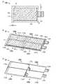
図1(A)は、本発明の一態様の表示装置に用いることができる表示パネル100の上面概略図である。また、図1(B)、(C)は、それぞれ図1(A)に示す一点鎖線X1−X2、X3−X4に対応する断面模式図の一例である。[Configuration example 1]
FIG. 1A is a schematic top view of a
表示パネル100は表示領域101と、表示領域101に隣接して、可視光を透過する領域110と、可視光を遮る領域120と、を備える。また、図1(A)では、表示パネル100にFPC(Flexible Printed Circuit)112が設けられている例を示す。 The
表示領域101は、表示を行う機能を有する。具体的には、表示領域101は、マトリクス状に配置された複数の画素を含み、画像を表示することが可能である。各画素には一つ以上の表示素子が設けられている。表示素子としては、代表的には有機EL素子などの発光素子、または液晶素子等を用いることができる。 The
図1(B)は表示領域101の断面模式図の一例である。表示パネル100はバリア層105およびバリア層115で発光素子130を挟持する構成となっている。また、発光面側にあるバリア層105は、接着層104を介して発光素子130上に設けられ、表示パネル100の表面に露出している。なお、ここでは表示素子の一例として有機EL素子である発光素子130を示している。 FIG. 1B is an example of a schematic cross-sectional view of the
図1(B)では表示パネル100はトランジスタ160を有する構成としているが、トランジスタを有していなくてもよい。また、表示パネル100は接着層118を介して基板108が設けられているが、表示パネル100が基板108を有していなくてもよい。また、バリア層105上にも基板を設ける構成、すなわち表示パネル100が一対の基板で挟持された構成としてもよい。また、表示パネル100がバリア層115を有さず、例えば基板108上にトランジスタ160等を設ける構成としてもよい。 In FIG. 1B, the
表示パネル100は、可撓性を有することが好ましい。そのために、基板108が可撓性を有することが好ましい。表示パネル100が可撓性を有することで、複数の表示パネル100を組み合わせる自由度を高くすることができる。 The
領域110には、例えば表示パネル100を構成する一対のバリア層、及び当該一対のバリア層に挟持された表示素子を封止するための封止材などが設けられていてもよい。このとき、領域110に設けられる部材には、可視光に対して透光性を有する材料を用いる。領域110の可視領域(波長が350nm以上750nm以下)の光に対する透過率の平均が70%以上であれば好ましく、80%以上であればより好ましく、90%以上であればさらに好ましい。 In the
図1(C)は領域110の断面模式図の一例である。バリア層105、バリア層115、接着層104、接着層118、および基板108は可視光に対して透光性を有する。また、表示領域101においてトランジスタ160を構成する層や発光素子130とトランジスタ160の間に位置する層が領域110に延在する場合は、それらの層も可視光に対して透光性を有する。 FIG. 1C is an example of a schematic cross-sectional view of the
領域120には、例えば表示領域101に含まれる画素に電気的に接続する配線が設けられている。また、このような配線に加え、画素を駆動するための駆動回路(走査線駆動回路、信号線駆動回路等)が設けられていてもよい。また、領域120はFPC112と電気的に接続する端子(接続端子ともいう)や、当該端子と電気的に接続する配線等が設けられている領域を含む。 In the
一対のバリア層が発光素子130を挟持する構成によって、表示パネル100の信頼性を高いものとすることができる。また、表示パネル100が表示面側に基板を有さないことで、発光素子130の発する光を外部に取り出す過程での損失を減らすことができる。 The structure in which the pair of barrier layers sandwich the light-emitting
バリア層105は、発光素子130よりも表示面側にあるため、可視光に対する透過性を有する。また、バリア層105およびバリア層115は、発光素子130へ水分等の不純物が浸入することを抑制する機能を有していることが好ましい。表示パネル100がバリア層115を有さない構成とする場合は、発光素子130に対して表示面と反対側に有する層、たとえば基板108が不純物の浸入を抑制する機能を有していることが好ましい。また、バリア層105およびバリア層115は表示パネル100の機械的強度を高める機能を有していてもよい。 Since the
バリア層105は単層でも積層でもよい。バリア層105は無機絶縁材料を含むことが好ましい。無機絶縁材料としては、例えば窒化アルミニウム、酸化アルミニウム、窒化酸化アルミニウム、酸化窒化アルミニウム、酸化マグネシウム、酸化ガリウム、窒化シリコン、酸化シリコン、窒化酸化シリコン、酸化窒化シリコン、酸化ゲルマニウム、酸化ジルコニウム、酸化ランタン、酸化ネオジム、酸化タンタルなどが挙げられる。なお、本明細書中において、窒化酸化とは、その組成として、酸素よりも窒素の含有量が多いものであって、酸化窒化とは、その組成として、窒素よりも酸素の含有量が多いものを示す。バリア層105が不純物の浸入を防ぐ機能を果たすために、厚さが10nm以上2μm以下であると好ましく、100nm以上1μm以下であるとより好ましい。 The
また、バリア層105は樹脂材料や金属材料を用いて形成してもよい。樹脂材料としては、後述する基板108に用いることのできる材料を参照できる。金属材料としては、特に限定はないが、例えば、アルミニウム、銅、鉄、チタン、ニッケル、または、アルミニウム合金もしくはステンレスなどの合金などを用いることができる。バリア層105に金属材料を用いる場合は、可視光に対して透光性を有する程度に薄い膜厚とすればよい。 The
バリア層105を厚くすると表示パネル100の機械的強度は増すため好ましい。一方で、表示パネル100が可撓性を有する程度に薄いことが好ましい。よって、バリア層105が表示パネル100の機械的強度を高めたい場合は、厚さが5μm以上100μm以下であることが好ましく、20μm以上50μm以下であるとより好ましい。 A
バリア層115は、バリア層105と同様の材料を用いて形成することができる。なお、バリア層115は可視光に対して透光性を有さなくてよいため、例えば、バリア層105及びバリア層115を金属材料を用いて形成する場合に、バリア層115をバリア層105より膜厚の厚い構成としてもよい。 The
本発明の一態様の表示装置10は、上述した表示パネル100を複数備える。図1(D)では、3つの表示パネル100を備える表示装置10の上面概略図を示す。また図1(E)に、図1(D)の一点鎖線X5−X6に対応する断面図を示す。 The
なお、以降では各々の表示パネル同士、各々の表示パネルに含まれる構成要素同士、または各々の表示パネルに関連する構成要素同士を区別するために、符号の後にアルファベットを付記して説明する。また特に説明のない場合には、最も下側(表示面側とは反対側)に配置される表示パネルまたは構成要素に対して「a」を付記し、その上側に順に配置される一以上の表示パネルおよびその構成要素に対しては、符号の後にアルファベットをアルファベット順に付記することとする。また特に説明のない限り、複数の表示パネルを備える構成を説明する場合であっても、各々の表示パネルまたは構成要素に共通する事項を説明する場合には、アルファベットを省略して説明する。 Hereinafter, in order to distinguish between the respective display panels, the constituent elements included in the respective display panels, or the constituent elements related to the respective display panels, an alphabet is added after the reference numerals for description. Unless otherwise specified, “a” is added to the display panel or component arranged on the lowermost side (opposite to the display surface side), and one or more arranged in order on the upper side. For the display panel and its components, alphabets are added in alphabetical order after the reference numerals. Unless otherwise specified, even when a configuration including a plurality of display panels is described, when description is made on matters common to the respective display panels or components, the description is omitted.
図1(D)及び(E)に示す表示装置10は、表示パネル100a、表示パネル100b、表示パネル100c、基板106及び接着層107を備える。基板106は、各表示パネルの表示面側の最表面にあるバリア層105と、接着層107を介して互いに重なるように設けられている。バリア層105(105a、105b、および105c)は接着層107と接して設けられている。なお、図1(D)では基板106及び接着層107を図示せず省略している。また、図1(E)ではバリア層105(105a、105b、および105c)はそれぞれ表示パネル100(100a、100b、および100c)に含まれている。 A
表示パネル100bは、その一部が表示パネル100aの上側(表示面側)に重ねて配置されている。具体的には、表示パネル100aの表示領域101aと表示パネル100bの可視光を透過する領域110bとが重畳するように配置されている。すなわち表示装置10において、基板106と、接着層107と、領域110bと、表示領域101aとが、この順番で互いに重なるように設けられている。 A part of the
また、表示パネル100cは、その一部が表示パネル100bの上側(表示面側)に重ねて配置されている。具体的には、表示パネル100bの表示領域101bと表示パネル100cの可視光を透過する領域110cとが重畳するように配置されている。すなわち表示装置10において、基板106と、接着層107と、領域110cと、表示領域101bとが、この順番で互いに重なるように設けられている。 Further, a part of the
表示領域101a上には可視光を透過する領域110bが重畳するため、表示領域101aの全体を表示面側から視認することが可能となる。同様に、表示領域101bも領域110cが重畳することでその全体を表示面側から視認することができる。したがって、表示領域101a、表示領域101bおよび表示領域101cが継ぎ目なく配置された領域を表示装置10の表示領域11とすることが可能となる。 Since an
ここで、図1(A)に示す領域110の幅Wは、0.5mm以上150mm以下、好ましくは1mm以上100mm以下、より好ましくは2mm以上50mm以下とすることが好ましい。領域110は封止領域としての機能を有するため、領域110の幅Wが大きいほど表示パネル100の端面と表示領域101との距離を長くすることができ、外部からの水などの不純物が表示領域101にまで侵入することを効果的に抑制することが可能となる。特に本構成例では表示領域101に隣接して領域110が設けられるため、領域110の幅Wを適切な値に設定することが重要である。例えば、表示素子として有機EL素子を用いた場合には領域110の幅Wを1mm以上とすることで、有機EL素子の劣化を効果的に抑制することができる。なお、領域110ではない他の部分においても、表示領域101の端部と表示パネル100の端面との距離が上述の範囲になるように設定することが好ましい。 Here, the width W of the
接着層107及び基板106は、可視光に対して透光性を有する。表示装置10において、接着層107及び基板106は表示パネル100aおよび表示パネル100bの上面を覆う構成としている。接着層107及び基板106を複数の表示パネル100に亘って設けることで、表示装置10の機械的強度を高めることができる。 The
接着層107及び基板106は、それぞれの屈折率とバリア層105の屈折率のうち、最も小さい屈折率が、最も大きい屈折率の80%以上、好ましくは90%以上、より好ましくは95%以上となるように材料を選択することが好ましい。このような屈折率を有する接着層107及び基板106を用いることで、表示パネル100が発する光の進路にある積層体(例えば、バリア層105c、接着層107、基板106)における屈折率段差を低減し、光を効率よく外部に取り出すことができる。なお、バリア層105cは、図1(E)に図示していないが、表示パネル100cの表示面側の最表面にある層であり(図1(B)参照)、図1(E)においてバリア層105c、接着層107、基板106がこの順で接している。 The
また、このような屈折率を有する接着層107及び基板106を表示パネル100aと表示パネル100bとの段差部を覆うように設けることで、当該段差部が視認しにくくなるため、表示装置10の表示領域11に表示される画像の表示品位を高めることができる。なお、本明細書等において屈折率とは、可視領域(波長が350nm以上750nm以下)における屈折率の平均値を指す。 In addition, since the
接着層107としては、例えば粘着性を有する材料、または熱硬化型樹脂や光硬化型樹脂、2液混合型の硬化性樹脂などの硬化性樹脂を用いることができる。例えば、アクリル樹脂、ウレタン樹脂、エポキシ樹脂、またはシリコーン樹脂やシロキサン結合を有する樹脂などの樹脂を用いることができる。また、後述する樹脂層131に用いる材料を、接着層107として用いてもよい。接着層104、接着層118としては、接着層107と同様の材料を用いることができる。 As the
特に、接着層107として光硬化型樹脂を用いることが好ましい。光硬化型樹脂を用いることで、表示パネル100が有する発光素子にダメージを与えず室温で硬化することができる。また、光を照射するまで硬化しないため、樹脂を塗布した後に表示パネル同士、または基板と表示パネル間の位置合わせを精密に行う時間を確保することができる。 In particular, it is preferable to use a photocurable resin as the
なお、紫外線等の光は照射によってトランジスタの特性に影響を与える場合がある。そのため紫外線硬化型樹脂等を用いる場合は、照射後から硬化を始めるまでに時間を要する樹脂を選び、基板や、表示パネル100の領域110などトランジスタを含まない領域に樹脂を塗布した後に光を照射することが好ましい。 Note that light such as ultraviolet rays may affect the characteristics of the transistor by irradiation. For this reason, when using an ultraviolet curable resin or the like, select a resin that requires a long time from the start of irradiation to curing, and irradiate light after applying the resin to a substrate or a region that does not include a transistor, such as the
基板106としては、フィルム状のプラスチック基板、例えば、ポリイミド(PI)、アラミド、ポリエチレンテレフタレート(PET)、ポリエーテルスルホン(PES)、ポリエチレンナフタレート(PEN)、ポリカーボネート(PC)、ナイロン、ポリエーテルエーテルケトン(PEEK)、ポリスルホン(PSF)、ポリエーテルイミド(PEI)、ポリアリレート(PAR)、ポリブチレンテレフタレート(PBT)、シリコーン樹脂などのプラスチック基板を用いることができる。また、基板106は、可撓性を有することが好ましい。また、基板106は、繊維なども含み、例えばプリプレグなども含んでいてもよい。また、基板106としては、樹脂フィルムに限定されず、パルプを連続シート加工した透明な不織布や、フィブロインと呼ばれるたんぱく質を含む人工くも糸繊維を含むシートや、これらと樹脂とを混合させた複合体、繊維幅が4nm以上100nm以下のセルロース繊維からなる不織布と樹脂膜の積層体、人工くも糸繊維を含むシートと樹脂膜の積層体を用いてもよい。基板108としては、基板106と同様の材料を用いることができる。 As the
なお、図1(E)に示す表示装置10において、表示領域101aと表示領域101b、ならびに表示領域101bと表示領域101cはそれぞれ端部が一致しているが、これに限られない。表示領域101aと表示領域101b、ならびに表示領域101bと表示領域101cがそれぞれ互いに重なる領域を有していてもよい。 Note that in the
[構成例2]
図1(D)及び(E)では一方向に複数の表示パネル100を重ねて配置する構成を示したが、縦方向および横方向の二方向に複数の表示パネル100を重ねて配置してもよい。[Configuration example 2]
Although FIGS. 1D and 1E illustrate a configuration in which a plurality of
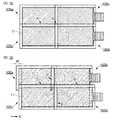
図2(A)は、図1(A)とは領域110の形状が異なる表示パネル100の例を示している。図2(A)に示す表示パネル100では、可視光を透過する領域110は表示領域101の2辺に沿って配置されている。 FIG. 2A illustrates an example of the
図2(B)に図2(A)に示した表示パネル100を縦2つ、横2つ配置した表示装置10の斜視概略図を示している。また図2(C)は、表示装置10の表示面側とは反対側から見たときの斜視概略図である。なお、図2(B)及び(C)において基板106及び接着層107は図示せず省略している。 FIG. 2B shows a schematic perspective view of the
図2(B)、(C)において、表示パネル100aの表示領域101aの短辺に沿った領域と、表示パネル100bの領域110bの一部が重畳して設けられている。また表示パネル100aの表示領域101aの長辺に沿った領域と、表示パネル100cの領域110cの一部が重畳して設けられている。また表示パネル100dの領域110dは、表示パネル100bの表示領域101bの長辺に沿った領域、及び表示パネル100cの表示領域101cの短辺に沿った領域に重畳して設けられている。 2B and 2C, an area along the short side of the
したがって、図2(B)に示すように、表示領域101a、表示領域101b、表示領域101cおよび表示領域101dが継ぎ目なく配置された領域を表示装置10の表示領域11とすることが可能となる。 Therefore, as shown in FIG. 2B, a region where the
ここで、表示パネル100が可撓性を有していることが好ましい。例えば図2(B)、(C)中の表示パネル100aに示すように、FPC112a等が表示面側に設けられる場合にFPC112aが設けられる側の表示パネル100aの一部を湾曲させ、FPC112aを隣接する表示パネル100bの表示領域101bの下側に重畳するように配置することができる。その結果、FPC112aを表示パネル100bの裏面と物理的に干渉することなく配置することができる。また、表示パネル100aと表示パネル100bとを重ねて接着する際に、FPC112aの厚さを考慮する必要がないため、表示パネル100bの領域110bの上面と、表示パネル100aの表示領域101aの上面との高さの差を低減できる。その結果、表示領域101a上に位置する表示パネル100bの端部が視認されてしまうことを抑制できる。 Here, it is preferable that the
さらに、各表示パネル100が可撓性を有することで、表示パネル100bの表示領域101bにおける上面の高さを、表示パネル100aの表示領域101aにおける上面の高さと一致するように、表示パネル100bを緩やかに湾曲させることができる。そのため、表示パネル100aと表示パネル100bとが重畳する領域近傍を除き、各表示領域の高さを揃えることができ、表示装置10の表示領域11に表示する画像の表示品位を高めることができる。 Furthermore, each
上記では、表示パネル100aと表示パネル100bの関係を例に説明したが、隣接する2つの表示パネル間でも同様である。 In the above description, the relationship between the
また、隣接する2つの表示パネル100間の段差を軽減するため、表示パネル100の厚さは薄いほうが好ましい。例えば表示パネル100の厚さを1mm以下、好ましくは300μm以下、より好ましくは100μm以下とすることが好ましい。 Moreover, in order to reduce the level | step difference between the two
図3(A)は、図2(B)、(C)に示す表示装置10を表示面側から見た上面概略図である。 FIG. 3A is a schematic top view of the
ここで、一つの表示パネル100の領域110の可視領域(波長が350nm以上750nm以下)の光に対する透過率を十分に高められない場合には、表示領域101と重なる表示パネル100の枚数に応じて、表示する画像の輝度が低下してしまう恐れがある。たとえば、図3(A)中の領域Aでは、表示パネル100aの表示領域101a上に1枚の表示パネル100cが重畳している。また領域Bでは、表示パネル100aの表示領域101a上に表示パネル100b、表示パネル100cおよび表示パネル100dの計3枚の表示パネル100が重畳している。 Here, in the case where the transmittance for light in the visible region (wavelength of 350 nm or more and 750 nm or less) of the
このような場合に、表示領域101上に重ねられる表示パネル100の枚数に応じて、画素の階調を局所的に高めるような補正を、表示させる画像データに対して施すことが好ましい。こうすることで、表示装置10の表示領域11に表示される画像の表示品位の低下を抑制することが可能となる。 In such a case, it is preferable to perform correction on the image data to be displayed so as to locally increase the gradation of the pixels in accordance with the number of
また、上部に配置する表示パネル100の位置をずらすことで、下部の表示パネル100の表示領域101上に重なる表示パネル100の枚数を低減することもできる。 Further, by shifting the position of the
図3(B)では、表示パネル100aおよび表示パネル100b上に配置する表示パネル100cおよび表示パネル100dを一方向(X方向)に領域110の幅Wの距離だけ相対的にずらして配置した場合を示している。このとき、一つの表示パネル100の表示領域101上に2つの表示パネル100が重ねられた領域Cと、1つの表示パネル100が重ねられた領域Dの2種類が存在する。 In FIG. 3B, the
なお、上部に位置する表示パネル100を相対的にずらして配置する場合には、各表示パネル100の表示領域101を組み合わせた領域の輪郭が矩形形状とは異なる形状となる。そのため、図3(B)で示すように表示装置10の表示領域11を矩形にする場合には、これよりも外側に位置する表示パネル100の表示領域101に画像を表示しないように表示装置10を駆動すればよい。このとき、画像を表示しない領域における画素の数を考慮し、表示領域11の全画素数を表示パネル100の枚数で割った数よりも多くの画素を、表示パネル100の表示領域101に設ければよい。 Note that, when the
なお、上記では、各々の表示パネル100を相対的にずらす場合の距離を、領域110の幅Wの整数倍としたがこれに限られず、表示パネル100の形状やこれを組み合わせた表示装置10の表示領域11の形状などを考慮して適宜設定すればよい。 In the above description, the distance when each
[断面構成例]
図4(A)は、図1(A)に示した表示パネル100を2つ貼り合せた際の表示装置10の断面概略図である。図4(A)では、FPC112aが表示パネル100aの表示面側に、またFPC112bが表示パネル100bの表示面側に、それぞれ接続されている構成を示している。[Section configuration example]
4A is a schematic cross-sectional view of the
また、図4(B)に示すように、FPC112aおよびFPC112bが表示パネル100aまたは表示パネル100bの表示面側とは反対側に接続される構成としてもよい。このような構成とすることで、下側に配置される表示パネル100aの端部を表示パネル100bの裏面に貼り付けることが可能なため、これらの接着面積を大きくでき、貼り合せ部分の機械的強度を高めることができる。 In addition, as illustrated in FIG. 4B, the
また、図4(C)に示すように、表示パネル100aおよび表示パネル100bの表示面とは反対側の面に樹脂層131と、樹脂層131を介して保護基板132を設ける構成としてもよい。このとき、樹脂層131は表示装置10と保護基板132とを接着する接着層としての機能を有していてもよい。このような構成とすることで、表示装置10の機械的強度をさらに高めることができる。 In addition, as illustrated in FIG. 4C, a structure in which a
樹脂層131に用いる材料としては、例えば、エポキシ樹脂、アラミド樹脂、アクリル樹脂、ポリイミド樹脂、ポリアミド樹脂、ポリアミドイミド樹脂等の有機樹脂を用いることができる。 As a material used for the
保護基板132としては、前述した基板106と同様の基板を用いることができる。 As the
また、図4(C)に示すように、表示パネル100aおよび表示パネル100bの裏面側に配置される樹脂層131および保護基板132には、FPC112aを取り出すための開口部116を設けることが好ましい。 As shown in FIG. 4C, the
表示面とは反対側に設けられる樹脂層131および保護基板132は、可視光に対して透光性を有している必要はなく、可視光を吸収または反射する材料を用いてもよい。なお、樹脂層131と接着層107、または保護基板132と基板106に同一の材料を共通して用いると、作製コストを低減することができる。 The
なお、接着層107および/または樹脂層131が、表示装置10の機械的強度を保つ程度に厚い場合は、基板106および/または保護基板132を設けない構成としてもよい。また、接着層107または樹脂層131のいずれか一方が、表示装置10の機械的強度を保つ程度に厚い場合は、基板106および保護基板132を設けず、かつ、接着層107または樹脂層131の他方を設けない構成としてもよい。図4(D)に、表示装置10が基板106および保護基板132を有さない場合の断面図を示す。図4(D)において表示装置10が基板106を有さないことで、図4(A)と比較して、表示パネル100aおよび表示パネル100bが有する発光素子の光を基板106の減衰分だけ多く取り出すことができる。 Note that in the case where the
また、図5(A)に示すように、表示パネル100aと表示パネル100bとが、接着層109により接着された構成としてもよい。表示パネル100aは表示面側の最表面にバリア層105aを有するため、図5(A)において、表示装置10は、バリア層105aと接着層109とが接する構成となっている。 Alternatively, as illustrated in FIG. 5A, the
このとき、接着層109がFPC112aの一部を覆って設けると、表示パネル100aとFPC112aとの接続部における機械的強度を高めることができ、FPC112aが剥がれてしまうなどの不具合を抑制できる。また、図5(B)には、表示装置10が接着層109を有し、FPC112aおよびFPC112bがそれぞれ表示パネル100a、表示パネル100bの表示面と反対側に設けられている構成を示す。 At this time, when the
接着層109としては、前述した接着層107と同様の材料を用いることが好ましい。ここで、接着層109の屈折率と、バリア層105aの屈折率のうち、小さい方の屈折率が、大きい方の屈折率の80%以上、好ましくは90%以上、より好ましくは95%以上となるように接着層109の材料を選択することが好ましい。このような屈折率を有する接着層109を用いることで、表示領域101aのうち可視光を透過する領域110bと重なる領域の発光素子が発する光を効率よく外部に取り出すことができる。 As the
表示装置10における接着層107および接着層109の構成は、図5(A)に示す限りではない。表示パネル100a、表示パネル100b及び基板106を接着する方法に応じて、上記構成は異なる形をとる。 The structures of the
例えば、まずFPC112aを有する表示パネル100aと、FPC112bを有する表示パネル100bを、接着層109を介して接着する(図5(C)参照)。その後に基板106を表示パネル100aおよび表示パネル100bに、接着層107を介して接着した場合、表示装置10における接着層107および接着層109の構成は図5(A)に示したようになる。 For example, first, the
また例えば、FPC112bを有する表示パネル100bを、接着層107を介して基板106に接着する。その後に基板106および表示パネル100bに、FPC112aを有する表示パネル100aを、接着層109を介して接着する。この場合、表示装置10における接着層107および接着層109の構成は図5(D)に示したようになる。 Further, for example, the
なお、表示パネル100aおよび表示パネル100bが、それぞれ基板108を有することで一定の機械的強度を備えている場合は、表示装置10に基板106及び接着層107を設けず、図5(C)に示した構成としてもよい。表示装置10が基板106を有さないことで、表示パネル100aおよび表示パネル100bが有する発光素子の発する光をより効率良く取り出すことができる。 Note that in the case where the
[表示領域の構成例]
続いて、表示パネル100の表示領域101の構成例について説明する。図6(A)は図2(A)における領域Pを拡大した上面概略図であり、図6(B)は領域Qを拡大した上面概略図である。[Display area configuration example]
Next, a configuration example of the
図6(A)に示すように、表示領域101には複数の画素141がマトリクス状に配置されている。赤、青、緑の3色を用いてフルカラー表示が可能な表示パネル100とする場合では、画素141は上記3色のうちいずれかを表示することのできる画素とする。または上記3色に加えて白や黄色を表示することのできる画素を設けてもよい。画素141を含む領域が表示領域101に相当する。 As shown in FIG. 6A, a plurality of
一つの画素141には配線142aおよび配線142bが電気的に接続されている。複数の配線142aのそれぞれは配線142bと交差し、回路143aと電気的に接続されている。また複数の配線142bは回路143bと電気的に接続されている。回路143aおよび回路143bのうち一方が走査線駆動回路として機能する回路であり、他方が信号線駆動回路として機能する回路とすることができる。なお、回路143aおよび回路143bのいずれか一方、または両方を設けない構成としてもよい。 A
図6(A)では、回路143aまたは回路143bに電気的に接続する複数の配線145が設けられている。配線145は、図示しない領域でFPC123と電気的に接続され、外部からの信号を回路143aおよび回路143bに供給する機能を有する。 In FIG. 6A, a plurality of
図6(A)において、回路143a、回路143b、複数の配線145を含む領域が、可視光を遮る領域120に相当する。 In FIG. 6A, a region including the
図6(B)において、最も端に設けられる画素141よりも外側の領域が可視光を透過する領域110に相当する。領域110は、画素141、配線142aおよび配線142b等の可視光を遮る部材を有していない。なお、画素141の一部、配線142aまたは配線142bが可視光に対して透光性を有する場合には、領域110にまで延在して設けられていてもよい。 In FIG. 6B, a region outside the
ここで、領域110の幅Wは、表示パネル100に設けられる領域110のうち、最も狭い幅を指す場合もある。表示パネル100の幅Wが場所によって異なる場合には、最も短い長さを幅Wとすることができる。なお、図6(B)では画素141から基板の端面までの距離(すなわち領域110の幅W)が、図面縦方向と横方向とで同一である場合を示している。 Here, the width W of the
図6(C)は図6(B)中の一点鎖線Y1−Y2における断面概略図である。図6(C)に示す表示パネル100は、それぞれ可視光に対して透光性を有する一対のバリア層(バリア層105、バリア層115)を有する。またバリア層105とバリア層115は接着層125によって接着されており、バリア層115には、接着層118を介して基板108が接着されている。画素141や配線142b等は、バリア層115上に形成される。 FIG. 6C is a schematic cross-sectional view taken along one-dot chain line Y1-Y2 in FIG. A
図6(B)、(C)に示すように、画素141が表示領域101の最も端に位置する場合には、可視光を透過する領域110の幅Wは、バリア層105または基板108の端部から画素141の端部までの長さとなる。 As shown in FIGS. 6B and 6C, when the
なお、画素141の端部とは、画素141に含まれる可視光を遮る部材のうち、最も端に位置する部材の端部を指す。または、画素141として一対の電極間に発光性の有機化合物を含む層を備える発光素子(有機EL素子ともいう)を用いた場合には、画素141の端部は下部電極の端部、発光性の有機化合物を含む層の端部、上部電極の端部のいずれかであってもよい。 Note that the end portion of the
図7(A)には、図6(B)に対して、配線142aの位置が異なる場合について示している。また図7(B)は図7(A)中の一点鎖線Y3−Y4における断面概略図であり、図7(C)は図7(A)中の一点鎖線Y5−Y6における断面概略図である。 FIG. 7A illustrates the case where the position of the
図7(A)、(B)、(C)に示すように、表示領域101の最も端に配線142aが位置する場合には、可視光を透過する領域110の幅Wは、バリア層105または基板108の端部から配線142aの端部までの長さとなる。なお、配線142aが可視光に対して透光性を有する場合には、配線142aが設けられる領域は領域110に含まれていてもよい。 As shown in FIGS. 7A, 7B, and 7C, when the
ここで、表示パネル100の表示領域101に設けられる画素の密度が高い場合、2つの表示パネル100を貼り合せた際に、位置ずれが生じてしまう場合がある。 Here, when the density of the pixels provided in the
図8(A)は、下部に設けられる表示パネル100aの表示領域101aと、上部に設けられる表示パネル100bの表示領域101bとの、表示面側から見たときの位置関係を示す図である。図8(A)には表示領域101aおよび表示領域101bのそれぞれの角部近傍を示している。表示領域101aの一部が、領域110bによって覆われている。 FIG. 8A is a diagram showing a positional relationship between the
図8(A)に示す例では、隣接する画素141aと画素141bとが相対的に一方向(Y方向)にずれた場合を示している。図中に示す矢印は、表示パネル100aが表示パネル100bに対してずれた方向を示している。また、図8(B)に示す例では、隣接する画素141aと画素141bとが相対的に縦方向および横方向(X方向およびY方向)の両方にずれた場合を示している。 In the example illustrated in FIG. 8A, a case where the
図8(A)および図8(B)に示す例では、横方向にずれた距離と縦方向にずれた距離がそれぞれ1画素分よりも小さい。このような場合は、表示領域101aまたは表示領域101bのいずれか一方に表示する画像の画像データに対し、当該ずれの距離に応じた補正を掛けることで表示品位を保つことが可能となる。具体的には、画素間の距離が小さくなるずれの場合には画素の階調(輝度)を低くするように補正し、画素間の距離が大きくなるずれの場合には、画素の階調(輝度)を高めるように補正すればよい。また、1画素分以上重なるようなずれの場合には、下部に位置する画素を駆動しないように画像データを一列分シフトさせるように補正すればよい。 In the example shown in FIGS. 8A and 8B, the distance shifted in the horizontal direction and the distance shifted in the vertical direction are each smaller than one pixel. In such a case, it is possible to maintain the display quality by applying correction corresponding to the distance of the shift to the image data of the image displayed in either the
図8(C)では、本来隣接するはずであった画素141aと画素141bとが、相対的に一方向(Y方向)に1画素分以上の距離でずれた例を示している。このように、1画素分の距離以上のずれが生じた場合には、突出した画素(ハッチングを付加した画素)を表示しないように駆動すればよい。なお、ずれの方向がX方向の場合においても同様である。 FIG. 8C illustrates an example in which the
なお、複数の表示パネル100を貼り合せる際には、位置ずれを抑制するように各々の表示パネル100に位置合わせのためのマーカー等を設けることが好ましい。または、表示パネル100の表面に凸部および凹部を形成し、2つの表示パネル100が重なる領域で当該凸部と凹部とを嵌合させる構成としてもよい。 In addition, when bonding a plurality of
また、位置ずれの精度を考慮して、表示パネル100の表示領域101にはあらかじめ使用する画素よりも多くの画素を配置しておくことが好ましい。例えば走査線に沿った画素列、または信号線に沿った画素列のうち、少なくとも一方を、1列以上、好ましくは3列以上、より好ましくは5列以上、表示に用いる画素列よりも余分に設けておくことが好ましい。 In consideration of the accuracy of positional deviation, it is preferable that more pixels than the pixels to be used are arranged in advance in the
[応用例]
本発明の一態様の表示装置10は、表示パネル100の数を増やすことにより、表示領域11の面積を上限なく大きくすることが可能である。したがって、表示装置10はデジタルサイネージやPIDなど、大きな画像を表示する用途に好適に用いることができる。[Application example]
The
図9(A)では、柱15や壁16に、本発明の一態様の表示装置10を適用した例を示している。表示装置10に用いる表示パネル100として、可撓性を有する表示パネルを用いることで、曲面に沿って表示装置10を設置することが可能となる。 FIG. 9A illustrates an example in which the
ここで、表示装置10に用いる表示パネル100の数が増えるほど、各々を駆動する信号を供給するための配線基板の規模が大きくなってしまう。さらに、表示装置10の面積が大きいほど長い配線が必要となるため信号の遅延が生じやすく、表示品位に悪影響を及ぼしてしまう場合がある。 Here, as the number of
そこで、表示装置10が備える複数の表示パネル100の各々に、表示パネル100を駆動する信号を供給する無線モジュールを設ける構成とすることが好ましい。 Therefore, it is preferable that each of the plurality of
図9(B)には、円柱状の柱15の表面に表示装置10を設置した場合の断面の例を示している。複数の表示パネル100を備える表示装置10は、内装部材21と外装部材22との間に配置され、柱15の表面に沿って湾曲している。 FIG. 9B shows an example of a cross section when the
一つの表示パネル100はFPC112を介して無線モジュール150(すなわち、図9(B)に示す無線モジュール150a乃至150dのいずれか一つ)と電気的に接続されている。表示パネル100は、内装部材21と外装部材22との間に設けられた支持部材23の上面側に支持され、無線モジュール150は支持部材23の下面側に配置されている。表示パネル100と無線モジュール150とは、支持部材23に設けられた開口部を介してFPC112によって電気的に接続されている。また、複数の表示パネル100(図9(B)においては、100a、100b、100c、及び100d)上に、接着層107を介して基板106が設けられている。 One
また、図9(B)では外装部材22の一部に遮光部26を備える構成を示している。遮光部26を、表示装置10の表示領域以外の領域を覆うように設けることで、当該領域が観察者に視認されない構成とすることができる。 FIG. 9B shows a configuration in which a
無線モジュール150は、柱15の内部または外部に設けられたアンテナ25から送信された無線信号27を受信する。また、無線モジュール150は、無線信号27から表示パネル100を駆動するための信号を抽出し、この信号を表示パネル100に供給する機能を有する。表示パネル100を駆動するための信号としては、電源電位、同期信号(クロック信号)、画像信号等がある。 The wireless module 150 receives the
例えば、各無線モジュール150にはそれぞれ固有番号が割り当てられている。またアンテナ25から送信される無線信号27には、固有番号を指定する信号と表示パネル100を駆動するための信号を含む。各無線モジュール150は無線信号27に含まれる固有番号が自己の固有番号に一致するときに、表示パネル100を駆動するための信号を受信し、これを表示パネル100にFPC112を介して供給することで、各表示パネル100に異なる画像を表示させることができる。 For example, each wireless module 150 is assigned a unique number. The
無線モジュール150は、無線信号27から電力を供給されるアクティブ型の無線モジュールであってもよいし、バッテリ等を内蔵したパッシブ型の無線モジュールであってもよい。パッシブ型の無線モジュールの場合、電磁誘導方式、磁界共鳴方式、電波方式等を用いた電力の授受(非接触電力伝送、無接点電力伝送あるいはワイヤレス給電などともいう)により、内蔵したバッテリを充電可能な構成としてもよい。 The wireless module 150 may be an active wireless module to which power is supplied from the
このような構成とすることで、大型の表示装置10であっても各表示パネル100を駆動するための信号に遅延が生じず、表示品位を高めることができる。また、無線信号27によって駆動するため、表示装置10を壁や柱に設置する際に、壁や柱に配線を通すための工事などが不要であり、あらゆる場所に容易に表示装置10を設置することが可能となる。同様に、表示装置10の設置箇所を変更することも容易である。 By adopting such a configuration, even in the
なお、上記では1つの表示パネル100につき1つの無線モジュール150を接続する構成としたが、2以上の表示パネル100につき1つの無線モジュール150を接続してもよい。 In the above description, one wireless module 150 is connected to one
例えば、本発明の一態様の表示装置は少なくとも2つの表示パネルを有していればよく、さらに、受信した無線信号から第1の信号を抽出し、これを第1の表示パネルに供給する第1の無線モジュールと、当該無線信号から第2の信号を抽出し、これを第2の表示パネルに供給する第2の無線モジュールと、を少なくとも備えていればよい。 For example, the display device of one embodiment of the present invention only needs to include at least two display panels, and further extracts a first signal from a received wireless signal and supplies the first signal to the first display panel. It is only necessary to include at least one wireless module and a second wireless module that extracts the second signal from the wireless signal and supplies the second signal to the second display panel.
本実施の形態は、少なくともその一部を本明細書中に記載する他の実施の形態と適宜組み合わせて実施することができる。 This embodiment can be implemented in appropriate combination with at least part of the other embodiments described in this specification.
(実施の形態2)
本実施の形態では、本発明の一態様の表示装置に適用可能な表示パネルの構成例について、図面を用いて説明する。(Embodiment 2)
In this embodiment, structural examples of display panels applicable to the display device of one embodiment of the present invention are described with reference to drawings.
本実施の形態では、主に有機EL素子を用いた表示パネルを例示するが、本発明の一態様の表示装置に用いることができる表示パネルはこれに限られない。本実施の形態で後に例示する、他の発光素子や表示素子を用いた発光パネル又は表示パネルも、本発明の一態様の表示装置に用いることができる。 In this embodiment, a display panel mainly using organic EL elements is exemplified; however, a display panel that can be used for the display device of one embodiment of the present invention is not limited thereto. A light-emitting panel or a display panel using another light-emitting element or display element, which will be exemplified later in this embodiment, can also be used for the display device of one embodiment of the present invention.
[構成例1]
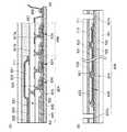
図10(A)に表示パネルの平面図を示し、図10(A)における一点鎖線A1−A2間の断面図の一例を図10(C)に示す。図10(C)には可視光を透過する領域110の断面図の一例も示す。[Configuration example 1]
FIG. 10A is a plan view of the display panel, and FIG. 10C illustrates an example of a cross-sectional view taken along dashed-dotted line A1-A2 in FIG. FIG. 10C also illustrates an example of a cross-sectional view of the
構成例1で示す表示パネルは、カラーフィルタ方式を用いたトップエミッション型の表示パネルである。本実施の形態において、表示パネルは、例えば、R(赤)、G(緑)、B(青)の3色の副画素で1つの色を表現する構成や、R、G、B、W(白)の4色の副画素で1つの色を表現する構成、R、G、B、Y(黄)の4色の副画素で1つの色を表現する構成等が適用できる。色要素としては特に限定はなく、RGBWY以外の色を用いてもよく、例えば、シアンやマゼンタ等を用いてもよい。 The display panel shown in the configuration example 1 is a top emission type display panel using a color filter method. In the present embodiment, for example, the display panel has a configuration in which one color is expressed by three sub-pixels of R (red), G (green), and B (blue), or R, G, B, W ( A configuration in which one color is expressed by sub-pixels of four colors (white), a configuration in which one color is expressed by sub-pixels of four colors of R, G, B, and Y (yellow) can be applied. The color element is not particularly limited, and colors other than RGBWY may be used. For example, cyan or magenta may be used.
図10(A)に示す表示パネルは、可視光を透過する領域110、発光部804、駆動回路部806、FPC808を有する。可視光を透過する領域110は、発光部804に隣接し、発光部804の2辺に沿って配置されている。 A display panel illustrated in FIG. 10A includes a
図10(C)に示す表示パネルは、基板701、接着層703、バリア層705、複数のトランジスタ(例えばトランジスタ820、826)、導電層857、絶縁層815、絶縁層817、複数の発光素子、絶縁層821、接着層822、着色層845、遮光層847、及びバリア層715を有する。接着層822、及びバリア層715は可視光を透過する。発光部804及び駆動回路部806に含まれる発光素子やトランジスタはバリア層705、バリア層715、及び接着層822によって封止されている。 A display panel illustrated in FIG. 10C includes a
発光部804は、接着層703、及びバリア層705を介して基板701上にトランジスタ820及び発光素子830を有する。発光素子830は、絶縁層817上の下部電極831と、下部電極831上のEL層833と、EL層833上の上部電極835と、を有する。下部電極831は、トランジスタ820のソース電極又はドレイン電極と電気的に接続する。下部電極831の端部は、絶縁層821で覆われている。下部電極831は可視光を反射することが好ましい。上部電極835は可視光を透過する。 The light-emitting
また、発光部804は、発光素子830と重なる着色層845と、絶縁層821と重なる遮光層847と、を有する。発光素子830と着色層845の間は接着層822で充填されている。 In addition, the light-emitting
絶縁層815は、トランジスタ820,826を構成する半導体への不純物の拡散を抑制する効果を奏する。また、絶縁層817は、該トランジスタ起因の表面凹凸を低減するために平坦化機能を有する絶縁層を選択することが好適である。 The insulating
駆動回路部806は、接着層703及びバリア層705を介して基板701上にトランジスタを複数有する。図10(C)では、駆動回路部806が含むトランジスタ826を示している。 The
バリア層705やバリア層715に防湿性の高い膜を用いることで、発光素子830やトランジスタ820に水等の不純物が侵入することを抑制でき、表示パネルの信頼性を高くすることができる。また、表示パネルが基板を有することで、物理的な衝撃から表示パネルの表面を保護することができるため好ましい。基板701は接着層703によってバリア層705と貼り合わされている。 By using a highly moisture-proof film for the
図10(C)に示す表示パネルは表示面と反対側に基板701を有するが、表示面側に基板を有していてもよく、また表示面側およびその反対側に一対の基板を有していてもよい。なお、表示面側に透過率の高い基板を設ける、または基板を設けないことで、発光素子830の光を効率良く外部に取り出すことができる。 The display panel illustrated in FIG. 10C includes a
なお、バリア層715を表面に露出させた積層体を作製する方法として、支持基板上にバリア層をはじめとする積層体を作製したのち、支持基板を剥離する方法がある。基板の剥離方法については後述する。 Note that as a method for manufacturing a stacked body in which the
導電層857は、駆動回路部806に外部からの信号(ビデオ信号、クロック信号、スタート信号、又はリセット信号等)や電位を伝達する外部入力端子と電気的に接続する。ここでは、外部入力端子としてFPC808を設ける例を示している。工程数の増加を防ぐため、導電層857は、発光部や駆動回路部に用いる電極や配線と同一の材料、同一の工程で作製することが好ましい。ここでは、導電層857を、トランジスタ820を構成する電極と同一の材料、同一の工程で作製した例を示す。 The
図10(C)に示す表示パネルでは、FPC808がバリア層715上に位置する。接続体825は、バリア層715、接着層822、絶縁層817、及び絶縁層815に設けられた開口を介して導電層857と接続している。また、接続体825はFPC808に接続している。接続体825を介してFPC808と導電層857は電気的に接続する。 In the display panel illustrated in FIG. 10C, the
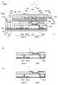
図10(C)に示す表示パネルを2枚重ねて有する表示装置の断面図の一例を図11に示す。図11では、下側の表示パネル100aの表示領域101a(図10(A)に示す発光部804と対応)及び可視光を遮る領域120a(図10(A)に示す駆動回路部806等に対応)、並びに、上側の表示パネル100bの表示領域101b(図10(A)に示す発光部804と対応)及び可視光を透過する領域110b(図10(A)に示す可視光を透過する領域110に対応)を示す。なお、図11に示す断面図は、実施の形態1で説明した表示装置10の断面構成例で示した図5(A)の領域170の一例でもある。 FIG. 11 illustrates an example of a cross-sectional view of a display device including two display panels illustrated in FIG. In FIG. 11, the
図11に示す表示装置において、表示面側(上側)に位置する表示パネルは、可視光を透過する領域110bを表示領域101bと隣接して有する。また、下側の表示パネルの表示領域101aと、上側の表示パネルの可視光を透過する領域110bとが重なっている。したがって、重ねた2つの表示パネルの表示領域の間の非表示領域を縮小すること、さらには無くすことができる。これにより、使用者から表示パネルの継ぎ目が認識されにくい、大型の表示装置を実現することができる。 In the display device illustrated in FIG. 11, the display panel located on the display surface side (upper side) includes a
また、図11に示す表示装置は、表示パネル100bの表示面側に接して、接着層107、基板106をこの順で備える構成となっている。表示パネル100bは表示面側の最表面にバリア層715bを有する。ここで、基板106、接着層107、およびバリア層715bのそれぞれの屈折率の差を小さくすることで、発光素子830bが発する光を効率よく外部に取り出すことができる。具体的には、基板106、接着層107、およびバリア層715bのそれぞれの屈折率のうち、最も小さい屈折率が最も大きい屈折率の80%以上、好ましくは90%以上、より好ましくは95%以上とすればよい。 In addition, the display device illustrated in FIG. 11 is configured to include the
例えば、基板106としてプラスチックフィルム(屈折率1.5程度)、接着層107として二液混合型のエポキシ樹脂(屈折率1.52程度)、バリア層715bとして酸化シリコン(屈折率1.46程度)を用いることで、これら積層体の屈折率段差を低減し、発光素子830bが発する光を効率よく取り出すことができる。 For example, a plastic film (refractive index of about 1.5) as the
また、図11に示す表示装置は、表示領域101aと可視光を透過する領域110bの間に、バリア層715aとの屈折率の差が小さく、可視光を透過する接着層109を有する。これにより、表示領域101aと可視光を透過する領域110bの間に空気が入ることを抑制でき、屈折率の差による界面での反射を低減することができる。そして、発光素子830aが発する光を効率よく取り出し、表示装置における表示ムラや輝度ムラの抑制が可能となる。 In addition, the display device illustrated in FIG. 11 includes an
具体的には、接着層109、バリア層715aのそれぞれの屈折率のうち、小さい方の屈折率が大きい方の屈折率の80%以上、好ましくは90%以上、より好ましくは95%以上とすればよい。なお、接着層109とバリア層715aの屈折率だけでなく、基板701bをはじめ発光素子830aの発する光の進路にある各層の屈折率ともそれぞれの値の差を小さくすることで、発光素子830aの発する光をより効率よく取り出すことができる。 Specifically, the refractive index of the smaller one of the refractive index of the
また、図11に示す表示装置は、接着層109により表示パネル100aおよび表示パネル100bを接着し、接着層107により表示パネル100a、表示パネル100bおよび基板106を接着する構成となっている。このようにすることで、個々の表示パネルの表示面側にそれぞれ基板を設ける構成と比較して、表示装置の物理的強度を高め、かつ表示装置の発する光の取り出し効率を上げることができる。 In addition, the display device illustrated in FIG. 11 has a structure in which the
[構成例2]
図10(B)に表示パネルの平面図を示し、図10(B)における一点鎖線A3−A4間の断面図の一例を図12(A)に示す。構成例2で示す表示パネルは、構成例1とは異なる、カラーフィルタ方式を用いたトップエミッション型の表示パネルである。ここでは、構成例1と異なる点のみ詳述し、構成例1と共通する点は説明を省略する。[Configuration example 2]
FIG. 10B is a plan view of the display panel, and FIG. 12A illustrates an example of a cross-sectional view taken along dashed-dotted line A3-A4 in FIG. The display panel shown in Configuration Example 2 is a top emission type display panel using a color filter method, which is different from Configuration Example 1. Here, only points different from the configuration example 1 will be described in detail, and the description of the points common to the configuration example 1 will be omitted.
図10(B)では、表示パネルの3辺にわたって可視光を透過する領域110を有する例を示す。そのうち、2辺において、可視光を透過する領域110は、発光部804と隣接している。 FIG. 10B illustrates an example having a
図12(A)に示す表示パネルは、図10(C)に示す表示パネルと下記の点で異なる。 The display panel shown in FIG. 12A is different from the display panel shown in FIG.
図12(A)に示す表示パネルは、絶縁層817a及び絶縁層817bを有し、絶縁層817a上に導電層856を有する。トランジスタ820のソース電極又はドレイン電極と、発光素子830の下部電極とが、導電層856を介して電気的に接続される。 The display panel illustrated in FIG. 12A includes an insulating
図12(A)に示す表示パネルは、絶縁層821上にスペーサ823を有する。スペーサ823を設けることで、基板701と基板711の間隔を調整することができる。 The display panel illustrated in FIG. 12A includes a
図12(A)に示す表示パネルは、着色層845及び遮光層847を覆うオーバーコート849を有する。発光素子830とオーバーコート849の間は接着層822で充填されている。 The display panel illustrated in FIG. 12A includes an
また、図12(A)に示す表示パネルは、バリア層715上に接着層713を介して基板711を有する。基板701と基板711とで大きさが異なる構成を示しているが、基板701と基板711の大きさが一致していてもよい。 In addition, the display panel illustrated in FIG. 12A includes a
なお、図12(B)に示すように、発光素子830は、下部電極831とEL層833の間に、光学調整層832を有していてもよい。光学調整層832には、可視光に対して透光性を有する導電性材料を用いることが好ましい。カラーフィルタ(着色層)とマイクロキャビティ構造(光学調整層)との組み合わせにより、本発明の一態様の表示装置からは、色純度の高い光を取り出すことができる。光学調整層の膜厚は、各副画素の色に応じて変化させればよい。 Note that as illustrated in FIG. 12B, the light-emitting
[構成例3]
図10(B)に表示パネルの平面図を示し、図10(B)における一点鎖線A3−A4間の断面図の一例を図12(C)に示す。構成例3で示す表示パネルは、塗り分け方式を用いたトップエミッション型の表示パネルである。[Configuration example 3]
FIG. 10B is a plan view of the display panel, and FIG. 12C illustrates an example of a cross-sectional view taken along dashed-dotted line A3-A4 in FIG. The display panel shown in the configuration example 3 is a top emission type display panel using a painting method.
図12(C)に示す表示パネルは、基板701、接着層703、バリア層705、複数のトランジスタ(例えばトランジスタ820、826)、導電層857、絶縁層815、絶縁層817、複数の発光素子、絶縁層821、スペーサ823、接着層822、バリア層715、及び基板711を有する。接着層822、バリア層715、及び基板711は可視光を透過する。 A display panel illustrated in FIG. 12C includes a
図12(C)に示す表示パネルでは、接続体825が絶縁層815上に位置する。接続体825は、絶縁層815に設けられた開口を介して導電層857と接続している。また、接続体825はFPC808に接続している。接続体825を介してFPC808と導電層857は電気的に接続する。 In the display panel illustrated in FIG. 12C, the
[構成例4]
図10(B)に表示パネルの平面図を示し、図10(B)における一点鎖線A3−A4間の断面図の一例を図13(A)に示す。構成例4で示す表示パネルは、カラーフィルタ方式を用いたボトムエミッション型の表示パネルである。[Configuration Example 4]
FIG. 10B is a plan view of the display panel, and FIG. 13A illustrates an example of a cross-sectional view taken along dashed-dotted line A3-A4 in FIG. The display panel shown in Configuration Example 4 is a bottom emission type display panel using a color filter method.
図13(A)に示す表示パネルは、バリア層705、複数のトランジスタ(例えばトランジスタ820、824、826)、導電層857、絶縁層815、着色層845、絶縁層817a、絶縁層817b、導電層856、複数の発光素子、絶縁層821、接着層822、及び基板711を有する。バリア層705、絶縁層815、絶縁層817a、及び絶縁層817bは可視光を透過する。 A display panel illustrated in FIG. 13A includes a
発光部804は、バリア層705上にトランジスタ820、トランジスタ824、及び発光素子830を有する。発光素子830は、絶縁層817b上の下部電極831と、下部電極831上のEL層833と、EL層833上の上部電極835と、を有する。下部電極831は、トランジスタ820のソース電極又はドレイン電極と電気的に接続する。下部電極831の端部は、絶縁層821で覆われている。上部電極835は可視光を反射することが好ましい。下部電極831は可視光を透過する。発光素子830と重なる着色層845を設ける位置は、特に限定されず、例えば、絶縁層817aと絶縁層817bの間や、絶縁層815と絶縁層817aの間等に設ければよい。 The light-emitting
駆動回路部806は、バリア層705上にトランジスタを複数有する。図13(A)では、駆動回路部806が有するトランジスタのうち、2つのトランジスタ826を示している。 The
バリア層705に防湿性の高い膜を用いることで、発光素子830やトランジスタ820、トランジスタ824に水等の不純物が侵入することを抑制でき、表示パネルの信頼性を高くすることができる。 By using a highly moisture-proof film for the
導電層857は、駆動回路部806に外部からの信号や電位を伝達する外部入力端子と電気的に接続する。ここでは、外部入力端子としてFPC808を設ける例を示している。また、ここでは、導電層857を、導電層856と同一の材料、同一の工程で作製した例を示す。 The
図13(A)に示す表示パネルは、表示面と反対側からFPCを取り出す構成となっている。そのため該表示パネルを、実施の形態1で説明した表示装置10を構成する表示パネルとして用いる場合、該表示パネルは図4(B)または図5(B)の構成に適用できる。 The display panel illustrated in FIG. 13A is configured to take out the FPC from the side opposite to the display surface. Therefore, when the display panel is used as a display panel included in the
[構成例5]
図13(B)に構成例1乃至4とは異なる発光パネルの例を示す。[Configuration Example 5]
FIG. 13B illustrates an example of a light-emitting panel which is different from the structural examples 1 to 4.
図13(B)に示す発光パネルは、基板701、接着層703、バリア層705、導電層814、導電層857a、導電層857b、発光素子830、絶縁層821、接着層822、バリア層715、及び基板711を有する。 A light-emitting panel illustrated in FIG. 13B includes a
導電層857a及び導電層857bは、発光パネルの外部接続電極であり、FPC等と電気的に接続させることができる。 The
発光素子830は、下部電極831、EL層833、及び上部電極835を有する。下部電極831の端部は、絶縁層821で覆われている。発光素子830はボトムエミッション型、トップエミッション型、又はデュアルエミッション型である。光を取り出す側の電極、基板、絶縁層等は、それぞれ可視光を透過する。導電層814は、下部電極831と電気的に接続する。 The light-emitting
光を取り出す側の基板は、光取り出し構造として、半球レンズ、マイクロレンズアレイ、凹凸構造が施されたフィルム、光拡散フィルム等を有していてもよい。例えば、樹脂基板上に上記レンズやフィルムを、該基板又は該レンズもしくはフィルムと同程度の屈折率を有する接着剤等を用いて接着することで、光取り出し構造を有する基板を形成することができる。 The substrate on the light extraction side may have a hemispherical lens, a microlens array, a film with a concavo-convex structure, a light diffusion film, or the like as the light extraction structure. For example, a substrate having a light extraction structure can be formed by adhering the lens or film on a resin substrate using an adhesive having the same refractive index as the substrate or the lens or film. .
導電層814は必ずしも設ける必要は無いが、下部電極831の抵抗に起因する電圧降下を抑制できるため、設けることが好ましい。また、同様の目的で、上部電極835と電気的に接続する導電層を絶縁層821上、EL層833上、又は上部電極835上などに設けてもよい。 The
導電層814は、銅、チタン、タンタル、タングステン、モリブデン、クロム、ネオジム、スカンジウム、ニッケル、アルミニウムから選ばれた材料又はこれらを主成分とする合金材料等を用いて、単層で又は積層して形成することができる。導電層814の膜厚は、例えば、0.1μm以上3μm以下とすることができ、好ましくは、0.1μm以上0.5μm以下である。 The
[材料および形成方法の一例]
次に、表示パネルまたは発光パネルに用いることができる材料等を説明する。なお、本明細書中で先に説明した構成については説明を省略する場合がある。[Example of material and forming method]
Next, materials that can be used for the display panel or the light-emitting panel will be described. In addition, description may be abbreviate | omitted about the structure demonstrated previously in this specification.
基板には、ガラス、石英、有機樹脂、金属、合金などの材料を用いることができる。発光素子からの光を取り出す側の基板は、該光を透過する材料を用いる。 For the substrate, materials such as glass, quartz, organic resin, metal, and alloy can be used. A substrate that extracts light from the light-emitting element is formed using a material that transmits the light.
特に、可撓性基板を用いることが好ましい。例えば、有機樹脂や可撓性を有する程度の厚さのガラス、金属、合金を用いることができる。 In particular, it is preferable to use a flexible substrate. For example, organic resin or flexible glass, metal, or alloy can be used.
ガラスに比べて有機樹脂は比重が小さいため、可撓性基板として有機樹脂を用いると、ガラスを用いる場合に比べて表示パネルを軽量化でき、好ましい。 Since the specific gravity of an organic resin is smaller than that of glass, it is preferable to use an organic resin as a flexible substrate because the display panel can be reduced in weight compared to the case of using glass.
基板には、靱性が高い材料を用いることが好ましい。これにより、耐衝撃性に優れ、破損しにくい表示パネルを実現できる。例えば、有機樹脂基板や、厚さの薄い金属基板もしくは合金基板を用いることで、ガラス基板を用いる場合に比べて、軽量であり、破損しにくい表示パネルを実現できる。 It is preferable to use a material having high toughness for the substrate. Thereby, it is possible to realize a display panel that has excellent impact resistance and is not easily damaged. For example, by using an organic resin substrate, a thin metal substrate, or an alloy substrate, it is possible to realize a display panel that is lighter and less likely to be damaged than when a glass substrate is used.
金属材料や合金材料は熱伝導性が高く、基板全体に熱を容易に伝導できるため、表示パネルの局所的な温度上昇を抑制することができ、好ましい。金属材料や合金材料を用いた基板の厚さは、10μm以上200μm以下が好ましく、20μm以上50μm以下であることがより好ましい。 Metal materials and alloy materials are preferable because they have high thermal conductivity and can easily conduct heat to the entire substrate, which can suppress a local temperature rise of the display panel. The thickness of the substrate using a metal material or an alloy material is preferably 10 μm to 200 μm, and more preferably 20 μm to 50 μm.
金属基板や合金基板を構成する材料としては、特に限定はないが、例えば、アルミニウム、銅、ニッケル、又は、アルミニウム合金もしくはステンレス等の金属の合金などを好適に用いることができる。 The material constituting the metal substrate or the alloy substrate is not particularly limited. For example, aluminum, copper, nickel, or an alloy of a metal such as an aluminum alloy or stainless steel can be preferably used.
また、基板に、熱放射率が高い材料を用いると表示パネルの表面温度が高くなることを抑制でき、表示パネルの破壊や信頼性の低下を抑制できる。例えば、基板を金属基板と熱放射率の高い層(例えば、金属酸化物やセラミック材料を用いることができる)の積層構造としてもよい。 In addition, when a material having a high thermal emissivity is used for the substrate, it is possible to suppress an increase in the surface temperature of the display panel, and it is possible to suppress destruction of the display panel and a decrease in reliability. For example, the substrate may have a stacked structure of a metal substrate and a layer having a high thermal emissivity (for example, a metal oxide or a ceramic material can be used).
可撓性を有する材料としては、例えば、実施の形態1で例示した基板106の材料が挙げられる。 As a material having flexibility, for example, the material of the
可撓性基板としては、上記材料を用いた層が、表示パネルの表面を傷などから保護するハードコート層(例えば、窒化シリコン層など)や、押圧を分散可能な材質の層(例えば、アラミド樹脂層など)等と積層されて構成されていてもよい。 As a flexible substrate, a layer using the above material is a hard coat layer (for example, a silicon nitride layer) that protects the surface of the display panel from scratches, or a layer (for example, aramid) that can disperse pressure. It may be configured to be laminated with a resin layer or the like.
可撓性基板は、複数の層を積層して用いることもできる。特に、ガラス層を有する構成とすると、水や酸素に対するバリア性を向上させ、信頼性の高い表示パネルとすることができる。 The flexible substrate can be used by stacking a plurality of layers. In particular, when the glass layer is used, the barrier property against water and oxygen can be improved and a highly reliable display panel can be obtained.
例えば、発光素子に近い側からガラス層、接着層、及び有機樹脂層を積層した可撓性基板を用いることができる。当該ガラス層の厚さとしては20μm以上200μm以下、好ましくは25μm以上100μm以下とする。このような厚さのガラス層は、水や酸素に対する高いバリア性と可撓性を同時に実現できる。また、有機樹脂層の厚さとしては、10μm以上200μm以下、好ましくは20μm以上50μm以下とする。このような有機樹脂層をガラス層よりも外側に設けることにより、ガラス層の割れやクラックを抑制し、機械的強度を向上させることができる。このようなガラス材料と有機樹脂の複合材料を基板に適用することにより、極めて信頼性が高いフレキシブルな表示パネルとすることができる。 For example, a flexible substrate in which a glass layer, an adhesive layer, and an organic resin layer are stacked from the side close to the light-emitting element can be used. The thickness of the glass layer is 20 μm or more and 200 μm or less, preferably 25 μm or more and 100 μm or less. The glass layer having such a thickness can simultaneously realize a high barrier property and flexibility against water and oxygen. The thickness of the organic resin layer is 10 μm or more and 200 μm or less, preferably 20 μm or more and 50 μm or less. By providing such an organic resin layer outside the glass layer, it is possible to suppress breakage and cracking of the glass layer and improve mechanical strength. By applying such a composite material of a glass material and an organic resin to a substrate, a flexible display panel with extremely high reliability can be obtained.
ここで、可撓性を有する表示パネルを形成する方法について説明する。 Here, a method for forming a flexible display panel will be described.
ここでは便宜上、画素や駆動回路を含む構成、カラーフィルタ等の光学部材を含む構成、タッチセンサ回路を含む構成、またはそのほかの機能性部材を含む構成を素子層と呼ぶこととする。素子層は例えば表示素子を含み、表示素子のほかに表示素子と電気的に接続する配線、画素や回路に用いるトランジスタなどの素子を備えていてもよい。 Here, for convenience, a configuration including a pixel and a drive circuit, a configuration including an optical member such as a color filter, a configuration including a touch sensor circuit, or a configuration including other functional members is referred to as an element layer. The element layer includes, for example, a display element, and may include an element such as a wiring that is electrically connected to the display element, a transistor used for a pixel, or a circuit in addition to the display element.
またここでは、素子層が形成される絶縁表面を備える支持体のことを、基材と呼ぶこととする。 Further, here, a support including an insulating surface on which an element layer is formed is referred to as a base material.
可撓性を有する基材上に素子層を形成する方法としては、基材上に直接素子層を形成する方法と、基材とは異なる剛性を有する支持基材上に素子層を形成した後、素子層と支持基材とを剥離して素子層を基材に転置する方法と、がある。 As a method of forming an element layer on a flexible substrate, a method of directly forming an element layer on a substrate, or after forming an element layer on a supporting substrate having rigidity different from that of the substrate There is a method of peeling the element layer and the supporting base material and transferring the element layer to the base material.
基材を構成する材料が、素子層の形成工程にかかる熱に対して耐熱性を有する場合には、基材上に直接素子層を形成すると、工程が簡略化されるため好ましい。このとき、基材を支持基材に固定した状態で素子層を形成すると、装置内、及び装置間における搬送が容易となるため好ましい。 When the material which comprises a base material has heat resistance with respect to the heat concerning the formation process of an element layer, when an element layer is directly formed on a base material, since a process is simplified, it is preferable. At this time, it is preferable to form the element layer in a state in which the base material is fixed to the supporting base material, because it is easy to carry the device inside and between the devices.
また、素子層を支持基材上に形成した後に、基材に転置する方法を用いる場合、まず支持基材上に剥離層と絶縁層を積層し、当該絶縁層上に素子層を形成する。続いて、支持基材から素子層を剥離し、基材に転置する。このとき、支持基材と剥離層の界面、剥離層と絶縁層の界面、または剥離層中で剥離が生じるような材料を選択すればよい。このような方法により、素子層の形成工程において基材の耐熱温度よりも高い温度での処理を行うことが可能となるため、表示パネルの信頼性を向上させることができる。 In the case of using a method in which an element layer is formed on a supporting substrate and then transferred to the substrate, a peeling layer and an insulating layer are first stacked on the supporting substrate, and an element layer is formed on the insulating layer. Subsequently, the element layer is peeled off from the support base material and transferred to the base material. At this time, a material that causes peeling in the interface between the support base and the release layer, the interface between the release layer and the insulating layer, or the release layer may be selected. By such a method, it becomes possible to perform processing at a temperature higher than the heat-resistant temperature of the base material in the element layer forming step, so that the reliability of the display panel can be improved.
例えば剥離層としてタングステンなどの高融点金属材料を含む層と、当該金属材料の酸化物を含む層を積層して用い、剥離層上に絶縁層として、窒化シリコンや酸窒化シリコンを複数積層した層を用いることが好ましい。高融点金属材料を用いると、素子層の形成時に高温の処理を行うことができ、信頼性を向上させることができる。例えば素子層に含まれる不純物をより低減することや、素子層に含まれる半導体などの結晶性をより高めることができる。また、基材としては、上述した可撓性を有する材料を好適に用いることができる。 For example, a layer containing a refractory metal material such as tungsten and a layer containing an oxide of the metal material are stacked as the separation layer, and a layer in which a plurality of silicon nitrides or silicon oxynitrides are stacked as an insulating layer over the separation layer Is preferably used. When a refractory metal material is used, high temperature treatment can be performed during formation of the element layer, and reliability can be improved. For example, impurities contained in the element layer can be further reduced, and crystallinity of a semiconductor or the like contained in the element layer can be further increased. Moreover, as a base material, the flexible material mentioned above can be used suitably.
なお、図10(C)や図13(A)に示す表示パネルは表示面側に基材を有さない構成であるが、これらの表示パネルは支持基材と素子層を剥離した後の、基材に転置する工程を省略することで作製することができる。実施の形態2で示す表示パネルおよび発光パネルをこの形成方法において形成する場合、バリア層705およびバリア層715が、支持基材を剥離する前の、剥離層との界面をなす絶縁層となる。 In addition, although the display panel shown in FIG.10 (C) or FIG.13 (A) is a structure which does not have a base material on the display surface side, these display panels have peeled the support base material and the element layer, It can be produced by omitting the step of transferring to the substrate. In the case where the display panel and the light-emitting panel described in
剥離は、機械的な力を加えて引き剥がすことや、剥離層をエッチングにより除去すること、または剥離界面の一部に液体を滴下して剥離界面全体に浸透させることなどにより行ってもよい。 Peeling may be performed by peeling off by applying a mechanical force, removing the peeling layer by etching, or dropping a liquid on a part of the peeling interface to infiltrate the whole peeling interface.
また、支持基材と絶縁層の界面で剥離が可能な場合には、剥離層を設けなくてもよい。例えば、支持基材としてガラスを用い、絶縁層としてポリイミドなどの有機樹脂を用いて、有機樹脂の一部をレーザ光等により局所的に加熱することにより剥離の起点を形成し、ガラスと絶縁層の界面で剥離を行ってもよい。または、支持基材と有機樹脂を含む絶縁層の間に、金属や半導体などの熱伝導性の高い材料の層を設け、これに電流を流して加熱することにより剥離しやすい状態とし、剥離を行ってもよい。このとき、有機樹脂を含む絶縁層は基材として用いることもできる。 In the case where peeling is possible at the interface between the support base and the insulating layer, the peeling layer may not be provided. For example, glass is used as a support base, an organic resin such as polyimide is used as an insulating layer, and a starting point of peeling is formed by locally heating a part of the organic resin with a laser beam or the like. Peeling may be performed at the interface. Alternatively, a layer of a material having high thermal conductivity such as a metal or a semiconductor is provided between the supporting base and the insulating layer containing an organic resin. You may go. At this time, the insulating layer containing an organic resin can also be used as a base material.
接着層には、紫外線硬化型等の光硬化型樹脂、反応硬化型樹脂、熱硬化型樹脂、嫌気型樹脂などの各種硬化型樹脂を用いることができる。これら樹脂としては、エポキシ樹脂、アクリル樹脂、シリコーン樹脂、フェノール樹脂、ポリイミド樹脂、イミド樹脂、PVC(ポリビニルクロライド)樹脂、PVB(ポリビニルブチラル)樹脂、EVA(エチレンビニルアセテート)樹脂等が挙げられる。特に、エポキシ樹脂等の透湿性が低い材料が好ましい。また、二液混合型の樹脂を用いてもよい。また、接着シート等を用いてもよい。 For the adhesive layer, various curable resins such as a photocurable resin such as an ultraviolet curable resin, a reactive curable resin, a thermosetting resin, and an anaerobic resin can be used. Examples of these resins include epoxy resins, acrylic resins, silicone resins, phenol resins, polyimide resins, imide resins, PVC (polyvinyl chloride) resins, PVB (polyvinyl butyral) resins, EVA (ethylene vinyl acetate) resins, and the like. In particular, a material with low moisture permeability such as an epoxy resin is preferable. Alternatively, a two-component mixed resin may be used. Further, an adhesive sheet or the like may be used.
また、上記樹脂に乾燥剤を含んでいてもよい。例えば、アルカリ土類金属の酸化物(酸化カルシウムや酸化バリウム等)のように、化学吸着によって水分を吸着する物質を用いることができる。又は、ゼオライトやシリカゲル等のように、物理吸着によって水分を吸着する物質を用いてもよい。乾燥剤が含まれていると、水分などの不純物が発光素子に侵入することを抑制でき、表示パネルの信頼性が向上するため好ましい。 Further, the resin may contain a desiccant. For example, a substance that adsorbs moisture by chemical adsorption, such as an alkaline earth metal oxide (such as calcium oxide or barium oxide), can be used. Alternatively, a substance that adsorbs moisture by physical adsorption, such as zeolite or silica gel, may be used. It is preferable that a desiccant be contained because impurities such as moisture can be prevented from entering the light-emitting element and the reliability of the display panel is improved.
また、上記樹脂に屈折率の高いフィラーや光散乱部材を混合することにより、発光素子からの光取り出し効率を向上させることができる。例えば、酸化チタン、酸化バリウム、ゼオライト、ジルコニウム等を用いることができる。 Moreover, the light extraction efficiency from a light emitting element can be improved by mixing the said resin with a filler with a high refractive index, or a light-scattering member. For example, titanium oxide, barium oxide, zeolite, zirconium, or the like can be used.
バリア層705およびバリア層715としては、防湿性の高い絶縁膜を用いることが好ましい。または、バリア層705およびバリア層715は、不純物の発光素子への拡散を防ぐ機能を有していることが好ましい。 As the
防湿性の高い絶縁膜としては、窒化シリコン膜、窒化酸化シリコン膜等の窒素と珪素を含む膜や、窒化アルミニウム膜等の窒素とアルミニウムを含む膜等が挙げられる。また、酸化シリコン膜、酸化窒化シリコン膜、酸化アルミニウム膜等を用いてもよい。また、実施の形態1で示したバリア層105に用いる材料を参照できる。 Examples of the highly moisture-proof insulating film include a film containing nitrogen and silicon such as a silicon nitride film and a silicon nitride oxide film, and a film containing nitrogen and aluminum such as an aluminum nitride film. Alternatively, a silicon oxide film, a silicon oxynitride film, an aluminum oxide film, or the like may be used. The material used for the
例えば、防湿性の高い絶縁膜の水蒸気透過量は、1×10⁻⁵[g/(m2・day)]以下、好ましくは1×10−6[g/(m2・day)]以下、より好ましくは1×10−7[g/(m2・day)]以下、さらに好ましくは1×10−8[g/(m2・day)]以下とする。For example, the moisture permeation amount of the highly moisture-proof insulating film is 1 × 10⁻⁵ [g / (m2 · day)] or less, preferably 1 × 10⁻⁶ [g / (m2 · day)] or less, More preferably, it is 1 × 10⁻⁷ [g / (m2 · day)] or less, and further preferably 1 × 10⁻⁸ [g / (m2 · day)] or less.
表示パネルにおいて、バリア層705又はバリア層715のうち、少なくとも発光面側のバリア層は、発光素子の発光を透過する必要がある。表示パネルがバリア層705及びバリア層715を有する場合、バリア層705又はバリア層715のうち、発光素子の発光を透過する側のバリア層は、他方のバリア層よりも、波長350nm以上750nm以下における透過率の平均が高いことが好ましい。 In the display panel, at least the barrier layer on the light emitting surface side of the
バリア層705やバリア層715は、酸素、窒素、及びシリコンを有することが好ましい。例えば、バリア層705やバリア層715は、酸化窒化シリコンを有することが好ましい。また、バリア層705やバリア層715は、窒化シリコン又は窒化酸化シリコンを有することが好ましい。また、バリア層705やバリア層715は、酸化窒化シリコン膜及び窒化シリコン膜を有し、該酸化窒化シリコン膜及び該窒化シリコン膜は接することが好ましい。酸化窒化シリコン膜と、窒化シリコン膜と、を交互に積層し、逆位相の干渉が可視領域で多く起こるようにすることで、積層体の可視領域における透過率を高めることができる。 The
表示パネルが有するトランジスタの構造は特に限定されない。例えば、スタガ型のトランジスタとしてもよいし、逆スタガ型のトランジスタとしてもよい。また、トップゲート型又はボトムゲート型のいずれのトランジスタ構造としてもよい。トランジスタに用いる半導体材料は特に限定されず、例えば、シリコン、ゲルマニウム、有機半導体等が挙げられる。又は、In−Ga−Zn系金属酸化物などの、インジウム、ガリウム、亜鉛のうち少なくとも一つを含む酸化物半導体を用いてもよい。 The structure of the transistor included in the display panel is not particularly limited. For example, a staggered transistor or an inverted staggered transistor may be used. Further, a top-gate or bottom-gate transistor structure may be employed. A semiconductor material used for the transistor is not particularly limited, and examples thereof include silicon, germanium, and an organic semiconductor. Alternatively, an oxide semiconductor containing at least one of indium, gallium, and zinc, such as an In—Ga—Zn-based metal oxide, may be used.
トランジスタに用いる半導体材料の結晶性についても特に限定されず、非晶質半導体、結晶性を有する半導体(微結晶半導体、多結晶半導体、単結晶半導体、又は一部に結晶領域を有する半導体)のいずれを用いてもよい。結晶性を有する半導体を用いると、トランジスタ特性の劣化を抑制できるため好ましい。 There is no particular limitation on the crystallinity of a semiconductor material used for the transistor, and any of an amorphous semiconductor and a semiconductor having crystallinity (a microcrystalline semiconductor, a polycrystalline semiconductor, a single crystal semiconductor, or a semiconductor partially including a crystal region) is used. May be used. It is preferable to use a crystalline semiconductor because deterioration of transistor characteristics can be suppressed.
トランジスタの特性安定化等のため、下地膜を設けることが好ましい。下地膜としては、酸化シリコン膜、窒化シリコン膜、酸化窒化シリコン膜、窒化酸化シリコン膜などの無機絶縁膜を用い、単層で又は積層して作製することができる。下地膜はスパッタリング法、CVD(Chemical Vapor Deposition)法(プラズマCVD法、熱CVD法、MOCVD(Metal Organic CVD)法など)、ALD(Atomic Layer Deposition)法、塗布法、印刷法等を用いて形成できる。なお、下地膜は、必要で無ければ設けなくてもよい。上記各構成例では、バリア層705がトランジスタの下地膜を兼ねることができる。 In order to stabilize the characteristics of the transistor, it is preferable to provide a base film. As the base film, an inorganic insulating film such as a silicon oxide film, a silicon nitride film, a silicon oxynitride film, or a silicon nitride oxide film can be used, which can be formed as a single layer or a stacked layer. The base film is formed by sputtering, CVD (Chemical Vapor Deposition) (plasma CVD, thermal CVD, MOCVD (Metal Organic CVD), etc.), ALD (Atomic Layer Deposition), coating, printing, etc. it can. Note that the base film is not necessarily provided if not necessary. In each of the above structural examples, the
発光素子としては、自発光が可能な素子を用いることができ、電流又は電圧によって輝度が制御される素子をその範疇に含んでいる。例えば、発光ダイオード(LED)、有機EL素子、無機EL素子等を用いることができる。 As the light-emitting element, an element capable of self-emission can be used, and an element whose luminance is controlled by current or voltage is included in its category. For example, a light emitting diode (LED), an organic EL element, an inorganic EL element, or the like can be used.
発光素子は、トップエミッション型、ボトムエミッション型、デュアルエミッション型のいずれであってもよい。光を取り出す側の電極には、可視光を透過する導電膜を用いる。また、光を取り出さない側の電極には、可視光を反射する導電膜を用いることが好ましい。 The light emitting element may be any of a top emission type, a bottom emission type, and a dual emission type. A conductive film that transmits visible light is used for the electrode from which light is extracted. In addition, a conductive film that reflects visible light is preferably used for the electrode from which light is not extracted.
可視光を透過する導電膜は、例えば、酸化インジウム、インジウム錫酸化物(ITO:Indium Tin Oxide)、インジウム亜鉛酸化物、酸化亜鉛(ZnO)、ガリウムを添加した酸化亜鉛などを用いて形成することができる。また、金、銀、白金、マグネシウム、ニッケル、タングステン、クロム、モリブデン、鉄、コバルト、銅、パラジウム、もしくはチタン等の金属材料、これら金属材料を含む合金、又はこれら金属材料の窒化物(例えば、窒化チタン)等も、可視光に対して透光性を有する程度に薄く形成することで用いることができる。また、上記材料の積層膜を導電層として用いることができる。例えば、銀とマグネシウムの合金とITOの積層膜などを用いると、導電性を高めることができるため好ましい。また、グラフェン等を用いてもよい。 The conductive film that transmits visible light is formed using, for example, indium oxide, indium tin oxide (ITO), indium zinc oxide, zinc oxide (ZnO), zinc oxide to which gallium is added, or the like. Can do. In addition, a metal material such as gold, silver, platinum, magnesium, nickel, tungsten, chromium, molybdenum, iron, cobalt, copper, palladium, or titanium, an alloy including these metal materials, or a nitride of these metal materials (for example, Titanium nitride) or the like can also be used by forming it thin enough to transmit visible light. In addition, a stacked film of the above materials can be used as a conductive layer. For example, it is preferable to use a laminated film of silver and magnesium alloy and ITO because the conductivity can be increased. Further, graphene or the like may be used.
可視光を反射する導電膜は、例えば、アルミニウム、金、白金、銀、ニッケル、タングステン、クロム、モリブデン、鉄、コバルト、銅、もしくはパラジウム等の金属材料、又はこれら金属材料を含む合金を用いることができる。また、上記金属材料や合金に、ランタン、ネオジム、又はゲルマニウム等が添加されていてもよい。また、アルミニウムとチタンの合金、アルミニウムとニッケルの合金、アルミニウムとネオジムの合金、アルミニウム、ニッケル、及びランタンの合金(Al−Ni−La)等のアルミニウムを含む合金(アルミニウム合金)や、銀と銅の合金、銀とパラジウムと銅の合金(Ag−Pd−Cu、APCとも記す)、銀とマグネシウムの合金等の銀を含む合金を用いて形成することができる。銀と銅を含む合金は、耐熱性が高いため好ましい。さらに、アルミニウム合金膜に接する金属膜又は金属酸化物膜を積層することで、アルミニウム合金膜の酸化を抑制することができる。該金属膜、金属酸化物膜の材料としては、チタン、酸化チタンなどが挙げられる。また、上記可視光を透過する導電膜と金属材料からなる膜とを積層してもよい。例えば、銀とITOの積層膜、銀とマグネシウムの合金とITOの積層膜などを用いることができる。 For the conductive film that reflects visible light, for example, a metal material such as aluminum, gold, platinum, silver, nickel, tungsten, chromium, molybdenum, iron, cobalt, copper, or palladium, or an alloy including these metal materials is used. Can do. In addition, lanthanum, neodymium, germanium, or the like may be added to the metal material or alloy. Also, alloys containing aluminum (aluminum alloys) such as aluminum and titanium alloys, aluminum and nickel alloys, aluminum and neodymium alloys, aluminum, nickel, and lanthanum alloys (Al-Ni-La), silver and copper Or an alloy containing silver such as an alloy of silver, palladium and copper (also referred to as Ag-Pd-Cu or APC), an alloy of silver and magnesium, or the like. An alloy containing silver and copper is preferable because of its high heat resistance. Furthermore, the oxidation of the aluminum alloy film can be suppressed by stacking the metal film or the metal oxide film in contact with the aluminum alloy film. Examples of the material for the metal film and metal oxide film include titanium and titanium oxide. Alternatively, the conductive film that transmits visible light and a film made of a metal material may be stacked. For example, a laminated film of silver and ITO, a laminated film of an alloy of silver and magnesium and ITO, or the like can be used.
電極は、それぞれ、蒸着法やスパッタリング法を用いて形成すればよい。そのほか、インクジェット法などの吐出法、スクリーン印刷法などの印刷法、又はメッキ法を用いて形成することができる。 The electrodes may be formed using a vapor deposition method or a sputtering method, respectively. In addition, it can be formed using a discharge method such as an inkjet method, a printing method such as a screen printing method, or a plating method.
下部電極831及び上部電極835の間に、発光素子の閾値電圧より高い電圧を印加すると、EL層833に陽極側から正孔が注入され、陰極側から電子が注入される。注入された電子と正孔はEL層833において再結合し、EL層833に含まれる発光物質が発光する。 When a voltage higher than the threshold voltage of the light-emitting element is applied between the
EL層833は少なくとも発光層を有する。EL層833は、発光層以外の層として、正孔注入性の高い物質、正孔輸送性の高い物質、正孔ブロック材料、電子輸送性の高い物質、電子注入性の高い物質、又はバイポーラ性の物質(電子輸送性及び正孔輸送性が高い物質)等を含む層をさらに有していてもよい。 The
EL層833には低分子系化合物及び高分子系化合物のいずれを用いることもでき、無機化合物を含んでいてもよい。EL層833を構成する層は、それぞれ、蒸着法(真空蒸着法を含む)、転写法、印刷法、インクジェット法、塗布法等の方法で形成することができる。 For the
発光素子830は、2以上の発光物質を含んでいてもよい。これにより、例えば、白色発光の発光素子を実現することができる。例えば2以上の発光物質の各々の発光が補色の関係となるように、発光物質を選択することにより白色発光を得ることができる。例えば、R(赤)、G(緑)、B(青)、Y(黄)、又はO(橙)等の発光を示す発光物質や、R、G、Bのうち2以上の色のスペクトル成分を含む発光を示す発光物質を用いることができる。例えば、青の発光を示す発光物質と、黄の発光を示す発光物質を用いてもよい。このとき、黄の発光を示す発光物質の発光スペクトルは、緑及び赤のスペクトル成分を含むことが好ましい。また、発光素子830の発光スペクトルは、可視領域の波長(例えば350nm以上750nm以下、又は400nm以上800nm以下など)の範囲内に2以上のピークを有することが好ましい。 The
EL層833は、複数の発光層を有していてもよい。EL層833において、複数の発光層は、互いに接して積層されていてもよいし、分離層を介して積層されていてもよい。例えば、蛍光発光層と、燐光発光層との間に、分離層を設けてもよい。 The
分離層は、例えば、燐光発光層中で生成する燐光材料等の励起状態から蛍光発光層中の蛍光材料等へのデクスター機構によるエネルギー移動(特に三重項エネルギー移動)を防ぐために設けることができる。分離層は数nm程度の厚さがあればよい。具体的には、0.1nm以上20nm以下、あるいは1nm以上10nm以下、あるいは1nm以上5nm以下である。分離層は、単一の材料(好ましくはバイポーラ性の物質)、又は複数の材料(好ましくは正孔輸送性材料及び電子輸送性材料)を含む。 The separation layer can be provided, for example, to prevent energy transfer (particularly triplet energy transfer) by a Dexter mechanism from an excited state of the phosphorescent material generated in the phosphorescent light emitting layer to the fluorescent material in the fluorescent light emitting layer. The separation layer may have a thickness of about several nm. Specifically, the thickness is 0.1 nm to 20 nm, or 1 nm to 10 nm, or 1 nm to 5 nm. The separation layer includes a single material (preferably a bipolar substance) or a plurality of materials (preferably a hole transport material and an electron transport material).
分離層は、該分離層と接する発光層に含まれる材料を用いて形成してもよい。これにより、発光素子の作製が容易になり、また、駆動電圧が低減される。例えば、燐光発光層が、ホスト材料、アシスト材料、及び燐光材料(ゲスト材料)からなる場合、分離層を、該ホスト材料及びアシスト材料で形成してもよい。上記構成を別言すると、分離層は、燐光材料を含まない領域を有し、燐光発光層は、燐光材料を含む領域を有する。これにより、分離層と燐光発光層とを燐光材料の有無の選択によって各々蒸着することが可能となる。また、このような構成とすることで、分離層と燐光発光層を同じチャンバーで成膜することが可能となる。これにより、製造コストを削減することができる。 The separation layer may be formed using a material included in the light emitting layer in contact with the separation layer. This facilitates the production of the light emitting element and reduces the driving voltage. For example, when the phosphorescent light-emitting layer is formed of a host material, an assist material, and a phosphorescent material (guest material), the separation layer may be formed using the host material and the assist material. In other words, the separation layer has a region not containing a phosphorescent material, and the phosphorescent light-emitting layer has a region containing a phosphorescent material. Thereby, the separation layer and the phosphorescent light emitting layer can be deposited by selecting the presence or absence of the phosphorescent material. Further, with such a structure, the separation layer and the phosphorescent light emitting layer can be formed in the same chamber. Thereby, manufacturing cost can be reduced.
また、発光素子830は、EL層を1つ有するシングル素子であってもよいし、電荷発生層を介して積層されたEL層を複数有するタンデム素子であってもよい。 The light-emitting
発光素子は、一対の防湿性の高い絶縁膜の間に設けられていることが好ましい。これにより、発光素子に水等の不純物が侵入することを抑制でき、表示パネルの信頼性の低下を抑制できる。 The light-emitting element is preferably provided between a pair of insulating films with high moisture resistance. Thereby, impurities such as water can be prevented from entering the light emitting element, and a decrease in the reliability of the display panel can be suppressed.
絶縁層815としては、例えば、酸化シリコン膜、酸化窒化シリコン膜、酸化アルミニウム膜などの無機絶縁膜を用いることができる。また、絶縁層817、絶縁層817a、及び絶縁層817bとしては、例えば、ポリイミド、アクリル、ポリアミド、ポリイミドアミド、ベンゾシクロブテン系樹脂等の有機材料をそれぞれ用いることができる。また、低誘電率材料(low−k材料)等を用いることができる。また、絶縁膜を複数積層させることで、各絶縁層を形成してもよい。 As the insulating
絶縁層821としては、有機絶縁材料又は無機絶縁材料を用いて形成する。樹脂としては、例えば、ポリイミド樹脂、ポリアミド樹脂、アクリル樹脂、シロキサン樹脂、エポキシ樹脂、又はフェノール樹脂等を用いることができる。特に感光性の樹脂材料を用い、下部電極831上に開口部を形成し、その開口部の側壁が連続した曲率を持って形成される傾斜面となるように形成することが好ましい。 The insulating
絶縁層821の形成方法は、特に限定されないが、フォトリソグラフィ法、スパッタ法、蒸着法、液滴吐出法(インクジェット法等)、印刷法(スクリーン印刷、オフセット印刷等)等を用いればよい。 A method for forming the insulating
スペーサ823は、無機絶縁材料、有機絶縁材料、金属材料等を用いて形成することができる。例えば、無機絶縁材料や有機絶縁材料としては、上記絶縁層に用いることができる各種材料が挙げられる。金属材料としては、チタン、アルミニウムなどを用いることができる。導電材料を含むスペーサ823と上部電極835とを電気的に接続させる構成とすることで、上部電極835の抵抗に起因した電位降下を抑制できる。また、スペーサ823は、順テーパ形状であっても逆テーパ形状であってもよい。 The
トランジスタの電極や配線、又は発光素子の補助電極等として機能する、表示パネルに用いる導電層は、例えば、モリブデン、チタン、クロム、タンタル、タングステン、アルミニウム、銅、ネオジム、スカンジウム等の金属材料又はこれらの元素を含む合金材料を用いて、単層で又は積層して形成することができる。また、導電層は、導電性の金属酸化物を用いて形成してもよい。導電性の金属酸化物としては酸化インジウム(In2O3等)、酸化スズ(SnO2等)、ZnO、ITO、インジウム亜鉛酸化物(In2O3−ZnO等)又はこれらの金属酸化物材料に酸化シリコンを含ませたものを用いることができる。A conductive layer used for a display panel that functions as an electrode or wiring of a transistor or an auxiliary electrode of a light-emitting element is a metal material such as molybdenum, titanium, chromium, tantalum, tungsten, aluminum, copper, neodymium, or scandium, or these An alloy material containing any of the above elements can be used to form a single layer or a stacked layer. The conductive layer may be formed using a conductive metal oxide. Examples of the conductive metal oxide include indium oxide (such as In2 O3 ), tin oxide (such as SnO2 ), ZnO, ITO, indium zinc oxide (such as In2 O3 —ZnO), or a metal oxide material thereof. The one containing silicon oxide can be used.
着色層は特定の波長帯域の光を透過する有色層である。例えば、赤色、緑色、青色、又は黄色の波長帯域の光を透過するカラーフィルタなどを用いることができる。各着色層は、様々な材料を用いて、印刷法、インクジェット法、フォトリソグラフィ法を用いたエッチング方法などでそれぞれ所望の位置に形成する。また、白色の副画素では、発光素子と重ねて透明又は白色等の樹脂を配置してもよい。 The colored layer is a colored layer that transmits light in a specific wavelength band. For example, a color filter that transmits light in a red, green, blue, or yellow wavelength band can be used. Each colored layer is formed at a desired position using various materials by a printing method, an inkjet method, an etching method using a photolithography method, or the like. In the white sub-pixel, a transparent or white resin may be disposed so as to overlap the light emitting element.
遮光層は、隣接する着色層の間に設けられている。遮光層は隣接する発光素子からの光を遮り、隣接する発光素子間における混色を抑制する。ここで、着色層の端部を、遮光層と重なるように設けることにより、光漏れを抑制することができる。遮光層としては、発光素子からの発光を遮る材料を用いることができ、例えば、金属材料や顔料や染料を含む樹脂材料を用いてブラックマトリクスを形成すればよい。なお、遮光層は、駆動回路部などの発光部以外の領域に設けると、導波光などによる意図しない光漏れを抑制できるため好ましい。 The light shielding layer is provided between the adjacent colored layers. The light shielding layer blocks light from adjacent light emitting elements and suppresses color mixing between adjacent light emitting elements. Here, light leakage can be suppressed by providing the end portion of the colored layer so as to overlap the light shielding layer. For the light-blocking layer, a material that blocks light emitted from the light-emitting element can be used. For example, a black matrix may be formed using a metal material, a resin material containing a pigment, or a dye. Note that the light shielding layer is preferably provided in a region other than the light emitting portion such as the drive circuit portion because unintended light leakage due to guided light or the like can be suppressed.
また、着色層及び遮光層を覆うオーバーコートを設けてもよい。オーバーコートを設けることで、着色層に含有された不純物等の発光素子への拡散を防止することができる。オーバーコートは、発光素子からの発光を透過する材料から構成され、例えば窒化シリコン膜、酸化シリコン膜等の無機絶縁膜や、アクリル膜、ポリイミド膜等の有機絶縁膜を用いることができ、有機絶縁膜と無機絶縁膜との積層構造としてもよい。 Moreover, you may provide the overcoat which covers a colored layer and a light shielding layer. By providing the overcoat, diffusion of impurities and the like contained in the colored layer to the light emitting element can be prevented. The overcoat is made of a material that transmits light emitted from the light emitting element. For example, an inorganic insulating film such as a silicon nitride film or a silicon oxide film, or an organic insulating film such as an acrylic film or a polyimide film can be used. A laminated structure of a film and an inorganic insulating film may be used.
また、接着層の材料を着色層及び遮光層上に塗布する場合、オーバーコートの材料として接着層の材料に対してぬれ性の高い材料を用いることが好ましい。例えば、オーバーコートとして、ITO膜などの酸化物導電膜や、可視光に対して透光性を有する程度に薄いAg膜等の金属膜を用いることが好ましい。 Further, when the material for the adhesive layer is applied on the colored layer and the light shielding layer, it is preferable to use a material having high wettability with respect to the material for the adhesive layer as the material for the overcoat. For example, it is preferable to use an oxide conductive film such as an ITO film or a metal film such as an Ag film that is thin enough to transmit visible light as the overcoat.
接続体としては、様々な異方性導電フィルム(ACF:Anisotropic Conductive Film)や、異方性導電ペースト(ACP:Anisotropic Conductive Paste)などを用いることができる。 As the connection body, various anisotropic conductive films (ACF: Anisotropic Conductive Film), anisotropic conductive pastes (ACP: Anisotropic Conductive Paste), and the like can be used.
本明細書等において、表示素子、表示素子を有するパネルである表示パネル、発光素子、及び発光素子を有するパネルである発光パネルは、様々な形態を用いること、又は様々な素子を有することができる。表示素子、表示パネル、発光素子又は発光パネルの一例としては、EL素子(有機物及び無機物を含むEL素子、有機EL素子、無機EL素子)、LED(白色LED、赤色LED、緑色LED、青色LEDなど)、トランジスタ(電流に応じて発光するトランジスタ)、電子放出素子、液晶素子、電子インク、電気泳動素子、グレーティングライトバルブ(GLV)、プラズマディスプレイパネル(PDP)、MEMS(マイクロ・エレクトロ・メカニカル・システム)を用いた表示素子、デジタルマイクロミラーデバイス(DMD)、DMS(デジタル・マイクロ・シャッター)、IMOD(インターフェアレンス・モジュレーション)素子、シャッター方式のMEMS表示素子、光干渉方式のMEMS表示素子、エレクトロウェッティング素子、圧電セラミックディスプレイ、カーボンナノチューブを用いた表示素子など、電気的または磁気的作用により、コントラスト、輝度、反射率、透過率などが変化する表示媒体を有するものがある。EL素子を用いた表示パネルの一例としては、ELディスプレイなどがある。電子放出素子を用いた表示パネルの一例としては、フィールドエミッションディスプレイ(FED)又はSED方式平面型ディスプレイ(SED:Surface−conduction Electron−emitter Display)などがある。液晶素子を用いた表示パネルの一例としては、液晶ディスプレイ(透過型液晶ディスプレイ、半透過型液晶ディスプレイ、反射型液晶ディスプレイ、直視型液晶ディスプレイ、投射型液晶ディスプレイ)などがある。電子インク、電子粉流体(登録商標)、又は電気泳動素子を用いた表示パネルの一例としては、電子ペーパーなどがある。なお、半透過型液晶ディスプレイや反射型液晶ディスプレイを実現する場合には、画素電極の一部又は全部が、反射電極としての機能を有するようにすればよい。例えば、画素電極の一部又は全部が、アルミニウム、銀などを有するようにすればよい。さらに、その場合、反射電極の下に、SRAMなどの記憶回路を設けることも可能である。これにより、さらに、消費電力を低減することができる。なお、LEDを用いる場合、LEDの電極や窒化物半導体の下に、グラフェンやグラファイトを配置してもよい。グラフェンやグラファイトは、複数の層を重ねて、多層膜としてもよい。このように、グラフェンやグラファイトを設けることにより、その上に、窒化物半導体、例えば、結晶を有するn型GaN半導体層などを容易に成膜することができる。さらに、その上に、結晶を有するp型GaN半導体層などを設けて、LEDを構成することができる。なお、グラフェンやグラファイトと、結晶を有するn型GaN半導体層との間に、AlN層を設けてもよい。なお、LEDが有するGaN半導体層は、MOCVDで成膜してもよい。ただし、グラフェンを設けることにより、LEDが有するGaN半導体層は、スパッタ法で成膜することも可能である。 In this specification and the like, a display element, a display panel which is a panel including a display element, a light-emitting element, and a light-emitting panel which is a panel including a light-emitting element can have various modes or have various elements. . Examples of display elements, display panels, light-emitting elements, or light-emitting panels include EL elements (EL elements including organic and inorganic substances, organic EL elements, inorganic EL elements), LEDs (white LEDs, red LEDs, green LEDs, blue LEDs, etc.) ), Transistor (transistor that emits light in response to current), electron-emitting device, liquid crystal device, electronic ink, electrophoretic device, grating light valve (GLV), plasma display panel (PDP), MEMS (micro electro mechanical system) ), Digital micromirror device (DMD), DMS (digital micro shutter), IMOD (interference modulation) element, shutter type MEMS display element, optical interference type MEMS display element, electro Wetti Grayed element, a piezoelectric ceramic display, or a display device using the carbon nanotube, the electric or magnetic action, those having contrast, brightness, reflectance, a display medium such as transmittance changes. An example of a display panel using an EL element is an EL display. As an example of a display panel using an electron-emitting device, there is a field emission display (FED), a SED type flat display (SED: Surface-Conduction Electron-Emitter Display), or the like. As an example of a display panel using a liquid crystal element, there is a liquid crystal display (a transmissive liquid crystal display, a transflective liquid crystal display, a reflective liquid crystal display, a direct view liquid crystal display, a projection liquid crystal display) and the like. An example of a display panel using electronic ink, electronic powder fluid (registered trademark), or an electrophoretic element is electronic paper. Note that in the case of realizing a transflective liquid crystal display or a reflective liquid crystal display, part or all of the pixel electrode may have a function as a reflective electrode. For example, part or all of the pixel electrode may have aluminum, silver, or the like. Further, in that case, a memory circuit such as an SRAM can be provided under the reflective electrode. Thereby, power consumption can be further reduced. In addition, when using LED, you may arrange | position graphene or graphite under the electrode and nitride semiconductor of LED. Graphene or graphite may be a multilayer film in which a plurality of layers are stacked. Thus, by providing graphene or graphite, a nitride semiconductor, for example, an n-type GaN semiconductor layer having a crystal can be easily formed thereon. Furthermore, a p-type GaN semiconductor layer having a crystal or the like can be provided thereon to form an LED. Note that an AlN layer may be provided between graphene or graphite and an n-type GaN semiconductor layer having a crystal. Note that the GaN semiconductor layer of the LED may be formed by MOCVD. However, by providing graphene, the GaN semiconductor layer of the LED can be formed by a sputtering method.
例えば、本明細書等において、画素に能動素子(アクティブ素子、非線形素子)を有するアクティブマトリクス方式、又は画素に能動素子を有しないパッシブマトリクス方式を用いることができる。 For example, in this specification and the like, an active matrix method in which an active element (an active element or a nonlinear element) is included in a pixel or a passive matrix method in which an active element is not included in a pixel can be used.
アクティブマトリクス方式では、トランジスタだけでなく、様々な能動素子を用いることができる。例えば、MIM(Metal Insulator Metal)、又はTFD(Thin Film Diode)などを用いることも可能である。これらの素子は、製造工程が少ないため、製造コストの低減、又は歩留まりの向上を図ることができる。又は、これらの素子は、素子のサイズが小さいため、開口率を向上させることができ、低消費電力化や高輝度化を図ることができる。 In the active matrix system, not only transistors but also various active elements can be used. For example, MIM (Metal Insulator Metal) or TFD (Thin Film Diode) can be used. Since these elements have few manufacturing steps, manufacturing cost can be reduced or yield can be improved. Alternatively, since these elements have small element sizes, the aperture ratio can be improved, and power consumption and luminance can be reduced.
パッシブマトリクス方式では、能動素子を用いないため、製造工程を少なくすることができ、製造コストの低減、又は歩留まりの向上を図ることができる。又は、パッシブマトリクス方式では、能動素子を用いないため、開口率を向上させることができ、低消費電力化、又は高輝度化などを図ることができる。 In the passive matrix method, since no active element is used, manufacturing steps can be reduced, manufacturing cost can be reduced, or yield can be improved. Alternatively, in the passive matrix method, an active element is not used, so that the aperture ratio can be improved and low power consumption, high luminance, or the like can be achieved.
なお、本発明の一態様の発光パネルは、表示パネルとして用いてもよいし、照明パネルとして用いてもよい。例えば、バックライトやフロントライトなどの光源、つまり、表示パネルのための照明パネルとして活用してもよい。 Note that the light-emitting panel of one embodiment of the present invention may be used as a display panel or an illumination panel. For example, it may be used as a light source such as a backlight or a front light, that is, a lighting panel for a display panel.
以上のように、本実施の形態で例示した、可視光を透過する領域を有する表示パネルを用いることで、表示パネルの継ぎ目が認識されにくく、表示ムラが抑制された、大型の表示装置を実現することができる。 As described above, by using the display panel having a region that transmits visible light, which is exemplified in this embodiment, a large display device in which a joint of the display panel is hardly recognized and display unevenness is suppressed is realized. can do.
本実施の形態は、他の実施の形態と適宜組み合わせることができる。 This embodiment can be combined with any of the other embodiments as appropriate.
(実施の形態3)
本実施の形態では、本発明の一態様の表示装置に用いることができるタッチパネルについて図面を用いて説明する。なお、実施の形態2で説明した表示パネルと同様の構成については、先の記載も参照することができる。また、本実施の形態では、発光素子を用いたタッチパネルを例示するが、これに限られない。例えば、実施の形態2に例示した他の素子(表示素子など)を用いたタッチパネルも本発明の一態様の表示装置に用いることができる。(Embodiment 3)
In this embodiment, a touch panel that can be used for the display device of one embodiment of the present invention will be described with reference to drawings. Note that the above description can be referred to for the structure similar to that of the display panel described in
[構成例1]
図14(A)はタッチパネルの上面図である。図14(B)は図14(A)の一点鎖線A−B間及び一点鎖線C−D間の断面図である。図14(C)は図14(A)の一点鎖線E−F間の断面図である。[Configuration example 1]
FIG. 14A is a top view of the touch panel. FIG. 14B is a cross-sectional view taken along the dashed-dotted line AB in FIG. 14A and between the dashed-dotted line CD. FIG. 14C is a cross-sectional view taken along alternate long and short dash line E-F in FIG.
図14(A)に示すタッチパネル390は、表示部301(入力部も兼ねる)、走査線駆動回路303g(1)、撮像画素駆動回路303g(2)、画像信号線駆動回路303s(1)、及び撮像信号線駆動回路303s(2)を有する。 A
表示部301は、複数の画素302と、複数の撮像画素308と、を有する。 The
画素302は、複数の副画素を有する。各副画素は、発光素子及び画素回路を有する。 The
画素回路は、発光素子を駆動する電力を供給することができる。画素回路は、選択信号を供給することができる配線と電気的に接続される。また、画素回路は、画像信号を供給することができる配線と電気的に接続される。 The pixel circuit can supply power for driving the light emitting element. The pixel circuit is electrically connected to a wiring that can supply a selection signal. The pixel circuit is electrically connected to a wiring that can supply an image signal.
走査線駆動回路303g(1)は、選択信号を画素302に供給することができる。 The scan
画像信号線駆動回路303s(1)は、画像信号を画素302に供給することができる。 The image signal
撮像画素308を用いてタッチセンサを構成することができる。具体的には、撮像画素308は、表示部301に触れる指等を検知することができる。 A touch sensor can be configured using the
撮像画素308は、光電変換素子及び撮像画素回路を有する。 The
撮像画素回路は、光電変換素子を駆動することができる。撮像画素回路は、制御信号を供給することができる配線と電気的に接続される。また、撮像画素回路は、電源電位を供給することができる配線と電気的に接続される。 The imaging pixel circuit can drive the photoelectric conversion element. The imaging pixel circuit is electrically connected to a wiring that can supply a control signal. The imaging pixel circuit is electrically connected to a wiring that can supply a power supply potential.
制御信号としては、例えば、記録された撮像信号を読み出す撮像画素回路を選択することができる信号、撮像画素回路を初期化することができる信号、及び撮像画素回路が光を検知する時間を決定することができる信号などを挙げることができる。 As the control signal, for example, a signal that can select an imaging pixel circuit that reads a recorded imaging signal, a signal that can initialize the imaging pixel circuit, and a time during which the imaging pixel circuit detects light are determined. The signal etc. which can be mentioned can be mentioned.
撮像画素駆動回路303g(2)は、制御信号を撮像画素308に供給することができる。 The imaging
撮像信号線駆動回路303s(2)は、撮像信号を読み出すことができる。 The imaging signal
図14(B)、(C)に示すように、タッチパネル390は、基板701、接着層703、バリア層705、基板711、接着層713、及びバリア層715を有する。また、基板701及び基板711は、接着層360で貼り合わされている。 As shown in FIGS. 14B and 14C, the
基板701とバリア層705は接着層703で貼り合わされている。また、基板711とバリア層715は接着層713で貼り合わされている。 The
基板701および基板711は、可撓性を有することが好ましい。 The
基板、接着層、及び絶縁層に用いることができる材料については実施の形態2を参照することができる。
画素302は、副画素302R、副画素302G、及び副画素302Bを有する(図14(C))。また、副画素302Rは発光モジュール380Rを有し、副画素302Gは発光モジュール380Gを有し、副画素302Bは発光モジュール380Bを有する。 The
例えば副画素302Rは、発光素子350R及び画素回路を有する。画素回路は、発光素子350Rに電力を供給することができるトランジスタ302tを含む。また、発光モジュール380Rは、発光素子350R及び光学素子(例えば赤色の光を透過する着色層367R)を有する。 For example, the
発光素子350Rは、下部電極351R、EL層353、及び上部電極352をこの順で積層して有する(図14(C))。 The light-emitting
EL層353は、第1のEL層353a、中間層354、及び第2のEL層353bをこの順で積層して有する。 The
なお、特定の波長の光を効率よく取り出せるように、発光モジュール380Rにマイクロキャビティ構造を配設することができる。具体的には、特定の光を効率よく取り出せるように配置された可視光を反射する膜及び半反射・半透過する膜の間にEL層を配置してもよい。 Note that a microcavity structure can be provided in the
例えば、発光モジュール380Rは、発光素子350Rと着色層367Rに接する接着層360を有する。 For example, the light-emitting
着色層367Rは発光素子350Rと重なる位置にある。これにより、発光素子350Rが発する光の一部は、空気よりも屈折率の高い接着層360及び着色層367Rを透過して、図中の矢印に示すように発光モジュール380Rの外部に射出される。 The
タッチパネル390は、遮光層367BMを有する。遮光層367BMは、着色層(例えば着色層367R)を囲むように設けられている。 The
タッチパネル390は、反射防止層367pを表示部301に重なる位置に有する。反射防止層367pとして、例えば円偏光板を用いることができる。 The
タッチパネル390は、絶縁層321を有する。絶縁層321はトランジスタ302t等を覆っている。なお、絶縁層321は画素回路や撮像画素回路に起因する凹凸を平坦化するための層として用いることができる。また、不純物のトランジスタ302t等への拡散を抑制することができる層が積層された絶縁層を、絶縁層321に適用することができる。 The
タッチパネル390は、下部電極351Rの端部に重なる隔壁328を有する。また、基板701と基板711の間隔を制御するスペーサ329を、隔壁328上に有する。 The
画像信号線駆動回路303s(1)は、トランジスタ303t及び容量303cを含む。なお、駆動回路は画素回路と同一の工程で同一基板上に形成することができる。図14(B)に示すようにトランジスタ303tは絶縁層321上に第2のゲート304を有していてもよい。第2のゲート304はトランジスタ303tのゲートと電気的に接続されていてもよいし、これらに異なる電位が与えられていてもよい。また、必要であれば、第2のゲート304をトランジスタ308t、トランジスタ302t等に設けてもよい。 The image signal
撮像画素308は、光電変換素子308p及び撮像画素回路を有する。撮像画素回路は、光電変換素子308pに照射された光を検知することができる。撮像画素回路は、トランジスタ308tを含む。 The
例えばpin型のフォトダイオードを光電変換素子308pに用いることができる。 For example, a pin-type photodiode can be used for the
タッチパネル390は、信号を供給することができる配線311を有し、端子319が配線311に設けられている。なお、画像信号及び同期信号等の信号を供給することができるFPC309が端子319に電気的に接続されている。なお、FPC309にはプリント配線基板(PWB)が取り付けられていてもよい。 The
なお、トランジスタ302t、トランジスタ303t、トランジスタ308t等のトランジスタは、同一の工程で形成することができる。又は、それぞれ異なる工程で形成してもよい。 Note that transistors such as the
[構成例2]
図15(A)、(B)は、タッチパネル505Aの斜視図である。なお明瞭化のため、代表的な構成要素を示す。図16(A)は、図15(A)に示す一点鎖線G−H間の断面図である。[Configuration example 2]
15A and 15B are perspective views of the
図15(A)、(B)に示すように、タッチパネル505Aは、表示部501、走査線駆動回路303g(1)、及びタッチセンサ595等を有する。また、タッチパネル505Aは、基板701、基板711、及び基板590を有する。 As shown in FIGS. 15A and 15B, the
タッチパネル505Aは、複数の画素及び複数の配線311を有する。複数の配線311は、画素に信号を供給することができる。複数の配線311は、基板701の外周部にまで引き回され、その一部が端子319を構成している。端子319はFPC509(1)と電気的に接続する。 The
タッチパネル505Aは、タッチセンサ595及び複数の配線598を有する。複数の配線598は、タッチセンサ595と電気的に接続される。複数の配線598は基板590の外周部に引き回され、その一部は端子を構成する。そして、当該端子はFPC509(2)と電気的に接続される。なお、図15(B)では明瞭化のため、基板590の裏面側(基板701に対向する面側)に設けられるタッチセンサ595の電極や配線等を実線で示している。 The
タッチセンサ595には、例えば静電容量方式のタッチセンサを適用できる。静電容量方式としては、表面型静電容量方式、投影型静電容量方式等がある。ここでは、投影型静電容量方式のタッチセンサを適用する場合を示す。 As the
投影型静電容量方式としては、主に駆動方式の違いから自己容量方式、相互容量方式などがある。相互容量方式を用いると同時多点検出が可能となるため好ましい。 As the projected capacitance method, there are mainly a self-capacitance method and a mutual capacitance method due to a difference in driving method. The mutual capacitance method is preferable because simultaneous multipoint detection is possible.
なお、タッチセンサ595には、指等の検知対象の近接又は接触を検知することができるさまざまなセンサを適用することができる。 Note that as the
投影型静電容量方式のタッチセンサ595は、電極591と電極592を有する。電極591は複数の配線598のいずれかと電気的に接続し、電極592は複数の配線598の他のいずれかと電気的に接続する。 The projected
電極592は、図15(A)、(B)に示すように、一方向に繰り返し配置された複数の四辺形が角部で接続された形状を有する。 As shown in FIGS. 15A and 15B, the
電極591は四辺形であり、電極592が延在する方向と交差する方向に繰り返し配置されている。なお、複数の電極591は、一の電極592と必ずしも直交する方向に配置される必要はなく、90度未満の角度をなすように配置されてもよい。 The
配線594は電極592と交差して設けられている。配線594は、電極592を挟む二つの電極591を電気的に接続する。このとき、電極592と配線594の交差部の面積ができるだけ小さくなる形状が好ましい。これにより、電極が設けられていない領域の面積を低減でき、透過率のムラを低減できる。その結果、タッチセンサ595を透過する光の輝度ムラを低減することができる。 The
なお、電極591、電極592の形状はこれに限られず、様々な形状を取りうる。例えば、複数の電極591をできるだけ隙間が生じないように配置し、絶縁層を介して電極592を、電極591と重ならない領域ができるように離間して複数設ける構成としてもよい。このとき、隣接する2つの電極592の間に、これらとは電気的に絶縁されたダミー電極を設けると、透過率の異なる領域の面積を低減できるため好ましい。 Note that the shapes of the
図16(A)に示すように、タッチパネル505Aは、基板701、接着層703、バリア層705、基板711、接着層713、及びバリア層715を有する。また、基板701及び基板711は、接着層360で貼り合わされている。 As shown in FIG. 16A, the
接着層597は、タッチセンサ595が表示部501に重なるように、基板590を基板711に貼り合わせている。接着層597は、可視光に対して透光性を有する。 The
電極591及び電極592は、可視光に対して透光性を有する導電材料を用いて形成する。透光性を有する導電性材料としては、酸化インジウム、インジウム錫酸化物、インジウム亜鉛酸化物、酸化亜鉛、ガリウムを添加した酸化亜鉛などの導電性酸化物を用いることができる。なお、グラフェンを含む膜を用いることもできる。グラフェンを含む膜は、例えば膜状に形成された酸化グラフェンを含む膜を還元して形成することができる。還元する方法としては、熱を加える方法等を挙げることができる。 The
また、電極591、電極592、配線594などの導電膜、つまり、タッチパネルを構成する配線や電極に用いる材料の抵抗値が低いことが望ましい。一例として、ITO、インジウム亜鉛酸化物、ZnO、銀、銅、アルミニウム、カーボンナノチューブ、グラフェンなどを用いてもよい。さらに、非常に細くした(例えば、直径が数ナノメートル)、多数の導電体を用いて構成される金属ナノワイヤを用いてもよい。一例としては、Agナノワイヤ、Cuナノワイヤ、又はAlナノワイヤ等を用いてもよい。Agナノワイヤの場合、例えば、89%以上の光透過率、40Ω/□以上100Ω/□以下のシート抵抗値を実現することができる。なお、透過率が高いため、表示素子に用いる電極、例えば、画素電極や共通電極に、金属ナノワイヤ、カーボンナノチューブ、グラフェンなどを用いてもよい。 In addition, it is preferable that the conductive film such as the
透光性を有する導電性材料を基板590上にスパッタリング法により成膜した後、フォトリソグラフィ法等の様々なパターニング技術により、不要な部分を除去して、電極591及び電極592を形成することができる。 A conductive material having a light-transmitting property is formed over the
電極591及び電極592は絶縁層593で覆われている。また、電極591に達する開口が絶縁層593に設けられ、配線594が隣接する電極591を電気的に接続する。透光性を有する導電性材料は、タッチパネルの開口率を高めることができるため、配線594に好適に用いることができる。また、電極591及び電極592より導電性の高い材料は、電気抵抗を低減できるため配線594に好適に用いることができる。 The
なお、絶縁層593及び配線594を覆う絶縁層を設けて、タッチセンサ595を保護することができる。 Note that an insulating layer that covers the insulating
また、接続層599は、配線598とFPC509(2)を電気的に接続する。 In addition, the
表示部501は、マトリクス状に配置された複数の画素を有する。画素は、構成例1と同様であるため、説明を省略する。 The
なお、様々なトランジスタをタッチパネルに適用できる。ボトムゲート型のトランジスタを適用する場合の構成を、図16(A)、(B)に示す。 Note that various transistors can be applied to the touch panel. A structure in the case of using a bottom-gate transistor is illustrated in FIGS.
例えば、酸化物半導体、アモルファスシリコン等を含む半導体層を、図16(A)に示すトランジスタ302t及びトランジスタ303tに適用することができる。 For example, a semiconductor layer containing an oxide semiconductor, amorphous silicon, or the like can be applied to the
例えば、レーザーアニールなどの処理により結晶化させた多結晶シリコンを含む半導体層を、図16(B)に示すトランジスタ302t及びトランジスタ303tに適用することができる。 For example, a semiconductor layer containing polycrystalline silicon which is crystallized by treatment such as laser annealing can be applied to the
また、トップゲート型のトランジスタを適用する場合の構成を、図16(C)に示す。 A structure in the case of using a top-gate transistor is illustrated in FIG.
例えば、多結晶シリコン又は単結晶シリコン基板等から転置された単結晶シリコン膜等を含む半導体層を、図16(C)に示すトランジスタ302t及びトランジスタ303tに適用することができる。 For example, a semiconductor layer including a single crystal silicon film or the like transferred from a polycrystalline silicon or a single crystal silicon substrate can be applied to the
[構成例3]
図17は、タッチパネル505Bの断面図である。本実施の形態で説明するタッチパネル505Bは、供給された画像情報をトランジスタが設けられている側に表示する点、タッチセンサが表示部の基板701側に設けられている点、及びFPC509(2)がFPC509(1)と同じ側に設けられている点が、構成例2のタッチパネル505Aとは異なる。ここでは異なる構成について詳細に説明し、同様の構成を用いることができる部分は、上記の説明を援用する。[Configuration example 3]
FIG. 17 is a cross-sectional view of the
着色層367Rは発光素子350Rと重なる位置にある。また、図17(A)に示す発光素子350Rは、トランジスタ302tが設けられている側に光を射出する。これにより、発光素子350Rが発する光の一部は着色層367Rを透過して、図中に示す矢印の方向の発光モジュール380Rの外部に射出される。 The
タッチパネル505Bは、光を射出する方向に遮光層367BMを有する。遮光層367BMは、着色層(例えば着色層367R)を囲むように設けられている。 The
タッチセンサ595は、基板711側でなく、基板701側に設けられている(図17(A))。 The
接着層597は、タッチセンサ595が表示部に重なるように、基板590を基板701に貼り合わせている。接着層597は、可視光に対して透光性を有する。 The
なお、ボトムゲート型のトランジスタを表示部501に適用する場合の構成を、図17(A)、(B)に示す。 Note that FIGS. 17A and 17B illustrate a structure in the case where a bottom-gate transistor is applied to the
例えば、酸化物半導体、アモルファスシリコン等を含む半導体層を、図17(A)に示すトランジスタ302t及びトランジスタ303tに適用することができる。 For example, a semiconductor layer containing an oxide semiconductor, amorphous silicon, or the like can be applied to the
例えば、多結晶シリコン等を含む半導体層を、図17(B)に示すトランジスタ302t及びトランジスタ303tに適用することができる。 For example, a semiconductor layer containing polycrystalline silicon or the like can be applied to the
また、トップゲート型のトランジスタを適用する場合の構成を、図17(C)に示す。 A structure in the case of using a top-gate transistor is illustrated in FIG.
例えば、多結晶シリコン又は転写された単結晶シリコン膜等を含む半導体層を、図17(C)に示すトランジスタ302t及びトランジスタ303tに適用することができる。 For example, a semiconductor layer including polycrystalline silicon, a transferred single crystal silicon film, or the like can be applied to the
[構成例4]
図18に示すように、タッチパネル500TPは、表示部500及び入力部600を重ねて有する。図19は、図18に示す一点鎖線Z1−Z2間の断面図である。[Configuration Example 4]
As illustrated in FIG. 18, the touch panel 500TP includes a
以下に、タッチパネル500TPを構成する個々の要素について説明する。なお、これらの構成は明確に分離できず、一つの構成が他の構成を兼ねる場合や他の構成の一部を含む場合がある。なお、表示部500に入力部600が重ねられたタッチパネル500TPをタッチパネルともいう。 Below, each element which comprises touch panel 500TP is explained. Note that these configurations cannot be clearly separated, and one configuration may serve as another configuration or may include a part of another configuration. Note that the touch panel 500TP in which the
入力部600は、マトリクス状に配設される複数の検知ユニット602を有する。また、入力部600は、選択信号線G1、制御線RES、信号線DLなどを有する。 The
選択信号線G1や制御線RESは、行方向(図中に矢印Rで示す)に配置される複数の検知ユニット602と電気的に接続される。信号線DLは、列方向(図中に矢印Cで示す)に配置される複数の検知ユニット602と電気的に接続される。 The selection signal line G1 and the control line RES are electrically connected to a plurality of
検知ユニット602は近接又は接触するものを検知して検知信号を供給する。例えば静電容量、照度、磁力、電波又は圧力等を検知して、検知した物理量に基づく情報を供給する。具体的には、容量素子、光電変換素子、磁気検知素子、圧電素子又は共振器等を検知素子に用いることができる。 The
検知ユニット602は、例えば、近接又は接触するものとの間の静電容量の変化を検知する。 The
なお、大気中において、指などの大気より大きな誘電率を有するものが導電膜に近接すると、指と導電膜の間の静電容量が変化する。この静電容量の変化を検知して検知情報を供給することができる。 Note that in the atmosphere, when an object having a dielectric constant greater than that of the atmosphere, such as a finger, approaches the conductive film, the capacitance between the finger and the conductive film changes. Detection information can be supplied by detecting the change in capacitance.
例えば、静電容量の変化に伴い容量素子との間で電荷の分配が引き起こされ、容量素子の両端の電極の電圧が変化する。この電圧の変化を検知信号に用いることができる。 For example, with the change in capacitance, charge is distributed to the capacitive element, and the voltage at the electrodes at both ends of the capacitive element changes. This change in voltage can be used as a detection signal.
検知ユニット602は検知回路を有する。検知回路は、選択信号線G1、制御線RES又は信号線DLなどに電気的に接続される。 The
検知回路は、トランジスタ又は/及び検知素子等を有する。例えば、導電膜と、当該導電膜に電気的に接続される容量素子と、を検知回路に用いることができる。また、容量素子と、当該容量素子に電気的に接続されるトランジスタと、を検知回路に用いることができる。 The detection circuit includes a transistor or / and a detection element. For example, a conductive film and a capacitor electrically connected to the conductive film can be used for the detection circuit. Further, a capacitor and a transistor electrically connected to the capacitor can be used for the detection circuit.
検知回路には、例えば、絶縁層653と、絶縁層653を挟持する第1の電極651及び第2の電極652と、を有する容量素子650を用いることができる(図19)。容量素子650の電極間の電圧は一方の電極に電気的に接続された導電膜にものが近接することにより変化する。 For the detection circuit, for example, a
検知ユニット602は、制御信号に基づいて導通状態又は非導通状態にすることができるスイッチを有する。例えば、トランジスタM12をスイッチに用いることができる。 The
また、検知信号を増幅するトランジスタを検知ユニット602に用いることができる。 A transistor that amplifies the detection signal can be used for the
同一の工程で作製することができるトランジスタを、検知信号を増幅するトランジスタ及びスイッチに用いることができる。これにより、作製工程が簡略化された入力部600を提供できる。 Transistors that can be manufactured in the same process can be used for transistors and switches that amplify a detection signal. Thereby, the
また、検知ユニット602はマトリクス状に配置された複数の窓部667を有する。窓部667は可視光を透過し、複数の窓部667の間に遮光性の層BMを配設してもよい。 The
タッチパネル500TPは、窓部667に重なる位置に着色層を有する。着色層は、所定の色の光を透過する。なお、着色層はカラーフィルタということができる。例えば、青色の光を透過する着色層367B、緑色の光を透過する着色層367G、又は赤色の光を透過する着色層367Rを用いることができる。また、黄色の光を透過する着色層や白色の光を透過する着色層を用いてもよい。 The touch panel 500TP has a colored layer at a position overlapping the
表示部500は、マトリクス状に配置された複数の画素302を有する。画素302は入力部600の窓部667と重なるように配置されている。画素302は、検知ユニット602に比べて高い精細度で配設されてもよい。画素は、構成例1と同様であるため、説明を省略する。 The
タッチパネル500TPは、可視光を透過する窓部667及びマトリクス状に配設される複数の検知ユニット602を有する入力部600と、窓部667に重なる画素302を複数有する表示部500と、を有し、窓部667と画素302の間に着色層を含んで構成される。また、それぞれの検知ユニットに他の検知ユニットへの干渉を低減することができるスイッチが配設されている。 The touch panel 500TP includes a
これにより、各検知ユニットが検知する検知情報を検知ユニットの位置情報と共に供給することができる。また、画像を表示する画素の位置情報に関連付けて検知情報を供給することができる。また、検知情報を供給させない検知ユニットと信号線を非導通状態にすることで、検知信号を供給させる検知ユニットへの干渉を低減することができる。その結果、利便性又は信頼性に優れた新規なタッチパネル500TPを提供することができる。 Thereby, the detection information which each detection unit detects can be supplied with the positional information on a detection unit. In addition, detection information can be supplied in association with position information of a pixel displaying an image. Moreover, the interference with the detection unit which supplies a detection signal can be reduced by making the detection unit which does not supply detection information, and a signal line into a non-conduction state. As a result, a novel touch panel 500TP that is highly convenient or reliable can be provided.
例えば、タッチパネル500TPの入力部600は検知情報を検知して位置情報と共に供給することができる。具体的には、タッチパネル500TPの使用者は、入力部600に触れた指等をポインタに用いて様々なジェスチャー(タップ、ドラッグ、スワイプ又はピンチイン等)をすることができる。 For example, the
入力部600は、入力部600に近接又は接触する指等を検知して、検知した位置又は軌跡等を含む検知情報を供給することができる。 The
演算装置は供給された情報が所定の条件を満たすか否かをプログラム等に基づいて判断し、所定のジェスチャーに関連付けられた命令を実行する。 The arithmetic device determines whether the supplied information satisfies a predetermined condition based on a program or the like, and executes a command associated with a predetermined gesture.
これにより、入力部600の使用者は、指等を用いて所定のジェスチャーを供給し、所定のジェスチャーに関連付けられた命令を演算装置に実行させることができる。 Thereby, the user of the
例えば、タッチパネル500TPの入力部600は、まず、一の信号線に検知情報を供給することができる複数の検知ユニットから一の検知ユニットXを選択する。そして、検知ユニットXを除いた他の検知ユニットと当該一の信号線を非導通状態にする。これにより、他の検知ユニットがもたらす検知ユニットXへの干渉を低減することができる。 For example, the
具体的には、他の検知ユニットの検知素子がもたらす検知ユニットXの検知素子への干渉を低減できる。 Specifically, the interference to the detection element of the detection unit X caused by the detection element of another detection unit can be reduced.
例えば、容量素子及び当該容量素子の一の電極が電気的に接続された導電膜を検知素子に用いる場合において、他の検知ユニットの導電膜の電位がもたらす、検知ユニットXの導電膜の電位への干渉を低減することができる。 For example, in the case where a conductive film in which a capacitor element and one electrode of the capacitor element are electrically connected is used as a detection element, the potential of the conductive film of the detection unit X is brought about by the potential of the conductive film of another detection unit. Interference can be reduced.
これにより、タッチパネル500TPはその大きさに依存することなく、検知ユニットを駆動して、検知情報を供給させることができる。例えば、ハンドヘルド型に用いることができる大きさから、電子黒板に用いることができる大きさまで、さまざまな大きさのタッチパネル500TPを提供することができる。 Thereby, touch panel 500TP can drive a detection unit and can supply detection information, without depending on the size. For example, the touch panel 500TP of various sizes can be provided from a size that can be used for a handheld type to a size that can be used for an electronic blackboard.
また、タッチパネル500TPは、折り畳まれた状態及び展開された状態にすることができる。そして、折り畳まれた状態と展開された状態とで、他の検知ユニットがもたらす検知ユニットXへの干渉が異なる場合においても、タッチパネル500TPの状態に依存することなく検知ユニットを駆動して、検知情報を供給させることができる。 Further, the touch panel 500TP can be in a folded state and an unfolded state. Even when the interference between the folded state and the unfolded state caused by the other detection units is different from the detection unit X, the detection unit is driven without depending on the state of the touch panel 500TP, and the detection information Can be supplied.
また、タッチパネル500TPの表示部500は表示情報を供給されることができる。例えば、演算装置は表示情報を供給することができる。 The
以上の構成に加えて、タッチパネル500TPは以下の構成を有することもできる。 In addition to the above configuration, the touch panel 500TP may have the following configuration.
タッチパネル500TPは、駆動回路603g又は駆動回路603dを有してもよい。また、FPC1と電気的に接続されてもよい。 The touch panel 500TP may include a
駆動回路603gは例えば所定のタイミングで選択信号を供給することができる。具体的には、選択信号を選択信号線G1ごとに所定の順番で供給する。また、さまざまな回路を駆動回路603gに用いることができる。例えば、シフトレジスタ、フリップフロップ回路、組み合わせ回路などを用いることができる。 The
駆動回路603dは、検知ユニット602が供給する検知信号に基づいて検知情報を供給する。また、さまざまな回路を駆動回路603dに用いることができる。例えば、検知ユニットに配設された検知回路と電気的に接続されることによりソースフォロワ回路やカレントミラー回路を構成することができる回路を、駆動回路603dに用いることができる。また、検知信号をデジタル信号に変換するアナログデジタル変換回路を有していてもよい。 The
FPC1は、タイミング信号、電源電位等を供給し、検知信号を供給される。 The
タッチパネル500TPは、駆動回路503g、駆動回路503s、配線311、又は端子319を有してもよい。また、FPC2と電気的に接続されてもよい。 The touch panel 500TP may include a
また、傷の発生を防いでタッチパネル500TPを保護する保護層670を有していてもよい。例えば、セラミックコート層又はハードコート層を保護層670に用いることができる。具体的には、酸化アルミニウムを含む層又はUV硬化樹脂を用いることができる。 Further, the
なお、半透過型液晶ディスプレイや反射型液晶ディスプレイを実現する場合には、画素電極の一部、又は、全部が、反射電極としての機能を有するようにすればよい。例えば、画素電極の一部、又は、全部が、アルミニウム、銀、などを有するようにすればよい。 Note that in the case of realizing a transflective liquid crystal display or a reflective liquid crystal display, part or all of the pixel electrode may have a function as a reflective electrode. For example, part or all of the pixel electrode may have aluminum, silver, or the like.
また、反射電極の下に、SRAMなどの記憶回路を設けることも可能である。これにより、さらに、消費電力を低減することができる。また、適用する表示素子に好適な構成を様々な画素回路から選択して用いることができる。 Further, a memory circuit such as an SRAM can be provided under the reflective electrode. Thereby, power consumption can be further reduced. In addition, a structure suitable for a display element to be applied can be selected from various pixel circuits and used.
本実施の形態で説明したタッチパネルを、実施の形態1の表示装置10を構成する表示パネル100のかわりに用いることができる。その場合、タッチパネル390やタッチパネル505Bのように、タッチパネルに接続される複数のFPCが一方向から取り出される構成のタッチパネルを好適に用いることができる。なお、表示パネル100のかわりにタッチパネルを用いた場合、表示装置10は入出力装置と呼ぶこともできる。 The touch panel described in this embodiment can be used instead of the
また、複数のタッチパネルを基板106と接着する接着層107を、それぞれのタッチパネルのタッチセンサ595(または入力部600)における上面の高さを一致させ、かつ該上面と基板106とが平行となるように設けることが好ましい。入出力装置の表面(すなわち基板106の表面)とそれぞれのタッチパネルのタッチセンサ595(または入力部600)との距離を等しくすることで、入出力装置の検出感度の場所依存性を小さくすることができる。 In addition, the
本実施の形態は、他の実施の形態と適宜組み合わせることができる。 This embodiment can be combined with any of the other embodiments as appropriate.
(実施の形態4)
本実施の形態では、本発明の一態様の電子機器及び照明装置について、図面を用いて説明する。(Embodiment 4)
In this embodiment, an electronic device and a lighting device of one embodiment of the present invention will be described with reference to drawings.
本発明の一態様の表示装置、表示パネル又はタッチパネルを用いて、曲面を有し、信頼性の高い電子機器や照明装置を作製できる。また、本発明の一態様の表示装置、表示パネル又はタッチパネルを用いて、可撓性を有し、信頼性の高い電子機器や照明装置を作製できる。 With the display device, the display panel, or the touch panel of one embodiment of the present invention, a highly reliable electronic device or lighting device having a curved surface can be manufactured. Further, with use of the display device, the display panel, or the touch panel of one embodiment of the present invention, a highly reliable electronic device or lighting device can be manufactured.
電子機器としては、例えば、テレビジョン装置(テレビ、又はテレビジョン受信機ともいう)、コンピュータ用などのモニタ、デジタルカメラ、デジタルビデオカメラ、デジタルフォトフレーム、携帯電話機(携帯電話、携帯電話装置ともいう)、携帯型ゲーム機、携帯情報端末、音響再生装置、パチンコ機などの大型ゲーム機などが挙げられる。 Examples of the electronic device include a television device (also referred to as a television or a television receiver), a monitor for a computer, a digital camera, a digital video camera, a digital photo frame, a mobile phone (also referred to as a mobile phone or a mobile phone device). ), Large game machines such as portable game machines, portable information terminals, sound reproducing devices, and pachinko machines.
また、本発明の一態様の電子機器又は照明装置は可撓性を有するため、家屋やビルの内壁もしくは外壁、又は、自動車の内装もしくは外装の曲面に沿って組み込むことも可能である。 In addition, since the electronic device or the lighting device of one embodiment of the present invention has flexibility, it can be incorporated along an inner wall or an outer wall of a house or a building, or a curved surface of an interior or exterior of an automobile.
また、本発明の一態様の電子機器は、二次電池を有していてもよく、非接触電力伝送を用いて、二次電池を充電することができると好ましい。 The electronic device of one embodiment of the present invention may include a secondary battery, and it is preferable that the secondary battery can be charged using non-contact power transmission.
二次電池としては、例えば、ゲル状電解質を用いるリチウムポリマー電池(リチウムイオンポリマー電池)等のリチウムイオン二次電池、リチウムイオン電池、ニッケル水素電池、ニカド電池、有機ラジカル電池、鉛蓄電池、空気二次電池、ニッケル亜鉛電池、銀亜鉛電池などが挙げられる。 Secondary batteries include, for example, lithium ion secondary batteries such as lithium polymer batteries (lithium ion polymer batteries) using a gel electrolyte, lithium ion batteries, nickel metal hydride batteries, nickel-cadmium batteries, organic radical batteries, lead storage batteries, air batteries A secondary battery, a nickel zinc battery, a silver zinc battery, etc. are mentioned.
本発明の一態様の電子機器は、アンテナを有していてもよい。アンテナで信号を受信することで、表示部で映像や情報等の表示を行うことができる。また、電子機器が二次電池を有する場合、アンテナを、非接触電力伝送に用いてもよい。 The electronic device of one embodiment of the present invention may include an antenna. By receiving a signal with an antenna, video, information, and the like can be displayed on the display unit. Further, when the electronic device has a secondary battery, the antenna may be used for non-contact power transmission.
図20(A)、(B)、(C1)、(C2)、(D)、(E)に、湾曲した表示部7000を有する電子機器の一例を示す。表示部7000はその表示面が湾曲して設けられ、湾曲した表示面に沿って表示を行うことができる。なお、表示部7000は可撓性を有していてもよい。 20A, 20B, 20C1, 2C, 2D, and 1E each illustrate an example of an electronic device having a
表示部7000は、本発明の一態様の表示装置、表示パネル又はタッチパネルを用いて作製される。 The
本発明の一態様により、湾曲した表示部を備え、且つ信頼性の高い電子機器を提供できる。 According to one embodiment of the present invention, a highly reliable electronic device including a curved display portion can be provided.
図20(A)に携帯電話機の一例を示す。携帯電話機7100は、筐体7101、表示部7000、操作ボタン7103、外部接続ポート7104、スピーカ7105、マイク7106等を有する。 FIG. 20A illustrates an example of a mobile phone. A
図20(A)に示す携帯電話機7100は、表示部7000にタッチセンサを備える。電話を掛ける、或いは文字を入力するなどのあらゆる操作は、指やスタイラスなどで表示部7000に触れることで行うことができる。 A
また、操作ボタン7103の操作により、電源のON、OFF動作や、表示部7000に表示される画像の種類を切り替えることができる。例えば、メール作成画面から、メインメニュー画面に切り替えることができる。 Further, by operating the
図20(B)にテレビジョン装置の一例を示す。テレビジョン装置7200は、筐体7201に表示部7000が組み込まれている。ここでは、スタンド7203により筐体7201を支持した構成を示している。 FIG. 20B illustrates an example of a television device. In the
図20(B)に示すテレビジョン装置7200の操作は、筐体7201が備える操作スイッチや、別体のリモコン操作機7211により行うことができる。または、表示部7000にタッチセンサを備えていてもよく、指等で表示部7000に触れることで操作してもよい。リモコン操作機7211は、当該リモコン操作機7211から出力する情報を表示する表示部を有していてもよい。リモコン操作機7211が備える操作キー又はタッチパネルにより、チャンネルや音量の操作を行うことができ、表示部7000に表示される映像を操作することができる。 Operation of the
なお、テレビジョン装置7200は、受信機やモデムなどを備えた構成としてもよい。受信機により一般のテレビ放送の受信を行うことができる。また、モデムを介して有線又は無線による通信ネットワークに接続することにより、一方向(送信者から受信者)又は双方向(送信者と受信者間、あるいは受信者間同士など)の情報通信を行うことも可能である。 Note that the
図20(C1)、(C2)、(D)、(E)に携帯情報端末の一例を示す。各携帯情報端末は、筐体7301及び表示部7000を有する。さらに、操作ボタン、外部接続ポート、スピーカ、マイク、アンテナ、又はバッテリ等を有していてもよい。表示部7000にはタッチセンサを備える。携帯情報端末の操作は、指やスタイラスなどで表示部7000に触れることで行うことができる。 Examples of portable information terminals are shown in FIGS. 20 (C1), (C2), (D), and (E). Each portable information terminal includes a
図20(C1)は、携帯情報端末7300の斜視図であり、図20(C2)は携帯情報端末7300の上面図である。図20(D)は、携帯情報端末7310の斜視図である。図20(E)は、携帯情報端末7320の斜視図である。 20C1 is a perspective view of the
本実施の形態で例示する携帯情報端末は、例えば、電話機、手帳又は情報閲覧装置等から選ばれた一つ又は複数の機能を有する。具体的には、スマートフォンとしてそれぞれ用いることができる。本実施の形態で例示する携帯情報端末は、例えば、移動電話、電子メール、文章閲覧及び作成、音楽再生、インターネット通信、コンピュータゲームなどの種々のアプリケーションを実行することができる。 The portable information terminal exemplified in this embodiment has one or a plurality of functions selected from, for example, a telephone, a notebook, an information browsing device, or the like. Specifically, each can be used as a smartphone. The portable information terminal exemplified in this embodiment can execute various applications such as mobile phone, e-mail, text browsing and creation, music playback, Internet communication, and computer games.
携帯情報端末7300、携帯情報端末7310及び携帯情報端末7320は、文字や画像情報をその複数の面に表示することができる。例えば、図20(C1)、(D)に示すように、3つの操作ボタン7302を一の面に表示し、矩形で示す情報7303を他の面に表示することができる。図20(C1)、(C2)では、携帯情報端末の上側に情報が表示される例を示し、図20(D)では、携帯情報端末の横側に情報が表示される例を示す。また、携帯情報端末の3面以上に情報を表示してもよく、図20(E)では、情報7304、情報7305、情報7306がそれぞれ異なる面に表示されている例を示す。 The
なお、情報の例としては、SNS(ソーシャル・ネットワーキング・サービス)の通知、電子メールや電話などの着信を知らせる表示、電子メールなどの題名もしくは送信者名、日時、時刻、バッテリの残量、アンテナ受信の強度などがある。または、情報が表示されている位置に、情報の代わりに、操作ボタン、アイコンなどを表示してもよい。 Examples of information include SNS (social networking service) notifications, displays that notify incoming calls such as e-mails and telephone calls, e-mail titles or sender names, date and time, time, battery level, antenna There is the strength of reception. Alternatively, an operation button, an icon, or the like may be displayed instead of the information at a position where the information is displayed.
例えば、携帯情報端末7300の使用者は、洋服の胸ポケットに携帯情報端末7300を収納した状態で、その表示(ここでは情報7303)を確認することができる。 For example, the user of the
具体的には、着信した電話の発信者の電話番号又は氏名等を、携帯情報端末7300の上方から観察できる位置に表示する。使用者は、携帯情報端末7300をポケットから取り出すことなく、表示を確認し、電話を受けるか否かを判断できる。 Specifically, the telephone number or name of the caller of the incoming call is displayed at a position where the
図21(A1)、(A2)、(B)乃至(I)に、可撓性を有する表示部7001を有する携帯情報端末の一例を示す。 FIGS. 21A1 to 21A illustrate an example of a portable information terminal including a
表示部7001は、本発明の一態様の表示装置、表示パネル又はタッチパネルを用いて作製される。例えば、曲率半径0.01mm以上150mm以下で曲げることができる表示装置、表示パネル又はタッチパネルを適用できる。また、表示部7001はタッチセンサを備えていてもよく、指等で表示部7001に触れることで携帯情報端末を操作することができる。 The
本発明の一態様により、可撓性を有する表示部を備え、且つ信頼性の高い電子機器を提供できる。 According to one embodiment of the present invention, a highly reliable electronic device including a flexible display portion can be provided.
図21(A1)は、携帯情報端末の一例を示す斜視図であり、図21(A2)は、携帯情報端末の一例を示す側面図である。携帯情報端末7500は、筐体7501、表示部7001、引き出し部材7502、操作ボタン7503等を有する。 FIG. 21A1 is a perspective view illustrating an example of a portable information terminal, and FIG. 21A2 is a side view illustrating an example of a portable information terminal. A
携帯情報端末7500は、筐体7501内にロール状に巻かれた可撓性を有する表示部7001を有する。 A
また、携帯情報端末7500は内蔵された制御部によって映像信号を受信可能で、受信した映像を表示部7001に表示することができる。また、携帯情報端末7500にはバッテリが内蔵されている。また、筐体7501にコネクターを接続する端子部を備え、映像信号や電力を有線により外部から直接供給する構成としてもよい。 Further, the
また、操作ボタン7503によって、電源のON、OFF動作や表示する映像の切り替え等を行うことができる。なお、図21(A1)、(A2)、(B)では、携帯情報端末7500の側面に操作ボタン7503を配置する例を示すが、これに限られず、携帯情報端末7500の表示面と同じ面(おもて面)や、表示面とは反対側の面に配置してもよい。 Further,
図21(B)には、表示部7001を引き出し部材7502により引き出した状態の携帯情報端末7500を示す。この状態で表示部7001に映像を表示することができる。また、表示部7001の一部がロール状に巻かれた図21(A1)の状態と表示部7001を引き出し部材7502により引き出した図21(B)の状態とで、携帯情報端末7500が異なる表示を行う構成としてもよい。例えば、図21(A1)の状態のときに、表示部7001のロール状に巻かれた部分を非表示とすることで、携帯情報端末7500の消費電力を下げることができる。 FIG. 21B illustrates the
なお、表示部7001を引き出した際に表示部7001の表示面が平面状となるように固定するため、表示部7001の側部に補強のためのフレームを設けていてもよい。 Note that a reinforcing frame may be provided on a side portion of the
なお、この構成以外に、筐体にスピーカを設け、映像信号と共に受信した音声信号によって音声を出力する構成としてもよい。 In addition to this configuration, a speaker may be provided in the housing, and audio may be output by an audio signal received together with the video signal.
図21(C)乃至(E)に、折りたたみ可能な携帯情報端末の一例を示す。図21(C)では、展開した状態、図21(D)では、展開した状態又は折りたたんだ状態の一方から他方に変化する途中の状態、図21(E)では、折りたたんだ状態の携帯情報端末7600を示す。携帯情報端末7600は、折りたたんだ状態では可搬性に優れ、展開した状態では、継ぎ目のない広い表示領域により一覧性に優れる。 FIGS. 21C to 21E illustrate an example of a foldable portable information terminal. In FIG. 21C, the portable information terminal is in the expanded state, in FIG. 21D, in the middle of changing from the expanded state or the folded state to the other, in FIG. 21E, in the folded state. 7600 is shown. The
表示部7001はヒンジ7602によって連結された3つの筐体7601に支持されている。ヒンジ7602を介して2つの筐体7601間を屈曲させることにより、携帯情報端末7600を展開した状態から折りたたんだ状態に可逆的に変形させることができる。 The
図21(F)、(G)に、折りたたみ可能な携帯情報端末の一例を示す。図21(F)では、表示部7001が内側になるように折りたたんだ状態、図21(G)では、表示部7001が外側になるように折りたたんだ状態の携帯情報端末7650を示す。携帯情報端末7650は表示部7001及び非表示部7651を有する。携帯情報端末7650を使用しない際に、表示部7001が内側になるように折りたたむことで、表示部7001の汚れや傷つきを抑制できる。 FIGS. 21F and 21G illustrate examples of portable information terminals that can be folded. FIG. 21F illustrates the
図21(H)に、可撓性を有する携帯情報端末の一例を示す。携帯情報端末7700は、筐体7701及び表示部7001を有する。さらに、入力手段であるボタン7703a、7703b、音声出力手段であるスピーカ7704a、7704b、外部接続ポート7705、マイク7706等を有していてもよい。また、携帯情報端末7700は、可撓性を有するバッテリ7709を搭載することができる。バッテリ7709は例えば表示部7001と重ねて配置してもよい。 FIG. 21H illustrates an example of a flexible portable information terminal. A
筐体7701、表示部7001、及びバッテリ7709は可撓性を有する。そのため、携帯情報端末7700を所望の形状に湾曲させることや、携帯情報端末7700に捻りを加えることが容易である。例えば、携帯情報端末7700は、表示部7001が内側又は外側になるように折り曲げて使用することができる。または、携帯情報端末7700をロール状に巻いた状態で使用することもできる。このように筐体7701及び表示部7001を自由に変形することが可能であるため、携帯情報端末7700は、落下した場合、又は意図しない外力が加わった場合であっても、破損しにくいという利点がある。 The
また、携帯情報端末7700は軽量であるため、筐体7701の上部をクリップ等で把持してぶら下げて使用する、又は、筐体7701を磁石等で壁面に固定して使用するなど、様々な状況において利便性良く使用することができる。 Further, since the
図21(I)に腕時計型の携帯情報端末の一例を示す。携帯情報端末7800は、バンド7801、表示部7001、入出力端子7802、操作ボタン7803等を有する。バンド7801は、筐体としての機能を有する。また、携帯情報端末7800は、可撓性を有するバッテリ7805を搭載することができる。バッテリ7805は例えば表示部7001やバンド7801と重ねて配置してもよい。 FIG. 21I illustrates an example of a wristwatch-type portable information terminal. A
バンド7801、表示部7001、及びバッテリ7805は可撓性を有する。そのため、携帯情報端末7800を所望の形状に湾曲させることが容易である。 The
操作ボタン7803は、時刻設定のほか、電源のオン、オフ動作、無線通信のオン、オフ動作、マナーモードの実行及び解除、省電力モードの実行及び解除など、様々な機能を持たせることができる。例えば、携帯情報端末7800に組み込まれたオペレーティングシステムにより、操作ボタン7803の機能を自由に設定することもできる。 The
また、表示部7001に表示されたアイコン7804に指等で触れることで、アプリケーションを起動することができる。 In addition, an application can be started by touching an
また、携帯情報端末7800は、通信規格された近距離無線通信を実行することが可能である。例えば無線通信可能なヘッドセットと相互通信することによって、ハンズフリーで通話することもできる。 In addition, the
また、携帯情報端末7800は入出力端子7802を有していてもよい。入出力端子7802を有する場合、他の情報端末とコネクターを介して直接データのやりとりを行うことができる。また入出力端子7802を介して充電を行うこともできる。なお、本実施の形態で例示する携帯情報端末の充電動作は、入出力端子を介さずに非接触電力伝送により行ってもよい。 Further, the
図22(A)に自動車9700の外観を示す。図22(B)に自動車9700の運転席を示す。自動車9700は、車体9701、車輪9702、ダッシュボード9703、ライト9704等を有する。本発明の一態様の表示装置は、自動車9700の備える表示部などに用いることができる。例えば、図22(B)に示す表示部9710乃至表示部9715に本発明の一態様の表示装置を設けることができる。 FIG. 22A illustrates the appearance of an
表示部9710と表示部9711は、自動車のフロントガラスに設けられた表示装置である。本発明の一態様の表示装置は、表示装置が有する電極を、透光性を有する導電性材料で作製することによって、反対側が透けて見える、いわゆるシースルー状態の表示装置とすることができる。シースルー状態の表示装置であれば、自動車9700の運転時にも視界の妨げになることがない。よって、本発明の一態様の表示装置を自動車9700のフロントガラスに設置することができる。なお、表示装置に、表示装置を駆動するためのトランジスタなどを設ける場合には、有機半導体材料を用いた有機トランジスタや、酸化物半導体を用いたトランジスタなど、透光性を有するトランジスタを用いるとよい。 A
表示部9712はピラー部分に設けられた表示装置である。例えば、車体に設けられた撮像手段からの映像を表示部9712に映し出すことによって、ピラーで遮られた視界を補完することができる。表示部9713はダッシュボード部分に設けられた表示装置である。例えば、車体に設けられた撮像手段からの映像を表示部9713に映し出すことによって、ダッシュボードで遮られた視界を補完することができる。すなわち、自動車の外側に設けられた撮像手段からの映像を映し出すことによって、死角を補い、安全性を高めることができる。また、見えない部分を補完する映像を映すことによって、より自然に違和感なく安全確認を行うことができる。 A
また、図23は、運転席と助手席にベンチシートを採用した自動車の室内を示している。表示部9721は、ドア部に設けられた表示装置である。例えば、車体に設けられた撮像手段からの映像を表示部9721に映し出すことによって、ドアで遮られた視界を補完することができる。また、表示部9722は、ハンドルに設けられた表示装置である。表示部9723は、ベンチシートの座面の中央部に設けられた表示装置である。なお、表示装置を座面や背もたれ部分などに設置して、当該表示装置を、当該表示装置の発熱を熱源としたシートヒーターとして利用することもできる。 FIG. 23 shows the interior of an automobile in which bench seats are used for the driver seat and the passenger seat. The
表示部9714、表示部9715、または表示部9722はナビゲーション情報、スピードメーターやタコメーター、走行距離、給油量、ギア状態、エアコンの設定など、その他様々な情報を表示することができる。また、表示部に表示される表示項目やレイアウトなどは、使用者の好みに合わせて適宜変更することができる。なお、上記情報は、表示部9710乃至表示部9713、表示部9721、表示部9723にも表示することができる。また、表示部9710乃至表示部9715、表示部9721乃至表示部9723は照明装置として用いることも可能である。また、表示部9710乃至表示部9715、表示部9721乃至表示部9723は加熱装置として用いることも可能である。 The
本実施の形態は、他の実施の形態と適宜組み合わせることができる。 This embodiment can be combined with any of the other embodiments as appropriate.
なお、本発明の一態様の表示装置を具備していれば、上記で示した電子機器や照明装置に特に限定されないことは言うまでもない。 Note that it is needless to say that the electronic device or the lighting device described above is not particularly limited as long as the display device of one embodiment of the present invention is included.
本実施の形態に示す構成及び方法などは、他の実施の形態に示す構成及び方法などと適宜組み合わせて用いることができる。 The structures and methods described in this embodiment can be combined as appropriate with any of the structures and methods described in the other embodiments.
10 表示装置
11 表示領域
15 柱
16 壁
21 内装部材
22 外装部材
23 支持部材
25 アンテナ
26 遮光部
27 無線信号
100 表示パネル
100a 表示パネル
100b 表示パネル
100c 表示パネル
100d 表示パネル
101 表示領域
101a 表示領域
101b 表示領域
101c 表示領域
101d 表示領域
104 接着層
105 バリア層
105a バリア層
105b バリア層
105c バリア層
106 基板
107 接着層
108 基板
109 接着層
110 領域
110b 領域
110c 領域
110d 領域
112 FPC
112a FPC
112b FPC
115 バリア層
116 開口部
118 接着層
120 領域
120a 領域
123 FPC
125 接着層
130 発光素子
131 樹脂層
132 保護基板
141 画素
141a 画素
141b 画素
142a 配線
142b 配線
143a 回路
143b 回路
145 配線
150 無線モジュール
160 トランジスタ
170 領域
301 表示部
302 画素
302B 副画素
302G 副画素
302R 副画素
302t トランジスタ
303c 容量
303g(1) 走査線駆動回路
303g(2) 撮像画素駆動回路
303s(1) 画像信号線駆動回路
303s(2) 撮像信号線駆動回路
303t トランジスタ
304 ゲート
308 撮像画素
308p 光電変換素子
308t トランジスタ
309 FPC
311 配線
319 端子
321 絶縁層
328 隔壁
329 スペーサ
350R 発光素子
351R 下部電極
352 上部電極
353 EL層
353a EL層
353b EL層
354 中間層
360 接着層
367B 着色層
367BM 遮光層
367G 着色層
367p 反射防止層
367R 着色層
380B 発光モジュール
380G 発光モジュール
380R 発光モジュール
390 タッチパネル
500 表示部
500TP タッチパネル
501 表示部
503g 駆動回路
503s 駆動回路
505A タッチパネル
505B タッチパネル
509 FPC
590 基板
591 電極
592 電極
593 絶縁層
594 配線
595 タッチセンサ
597 接着層
598 配線
599 接続層
600 入力部
602 検知ユニット
603d 駆動回路
603g 駆動回路
650 容量素子
651 電極
652 電極
653 絶縁層
667 窓部
670 保護層
701 基板
701b 基板
703 接着層
705 バリア層
711 基板
713 接着層
715 バリア層
715a バリア層
715b バリア層
804 発光部
806 駆動回路部
808 FPC
814 導電層
815 絶縁層
817 絶縁層
817a 絶縁層
817b 絶縁層
820 トランジスタ
821 絶縁層
822 接着層
823 スペーサ
824 トランジスタ
825 接続体
826 トランジスタ
830 発光素子
830a 発光素子
830b 発光素子
831 下部電極
832 光学調整層
833 EL層
835 上部電極
845 着色層
847 遮光層
849 オーバーコート
856 導電層
857 導電層
857a 導電層
857b 導電層
7000 表示部
7001 表示部
7100 携帯電話機
7101 筐体
7103 操作ボタン
7104 外部接続ポート
7105 スピーカ
7106 マイク
7200 テレビジョン装置
7201 筐体
7203 スタンド
7211 リモコン操作機
7300 携帯情報端末
7301 筐体
7302 操作ボタン
7303 情報
7304 情報
7305 情報
7306 情報
7310 携帯情報端末
7320 携帯情報端末
7500 携帯情報端末
7501 筐体
7502 引き出し部材
7503 操作ボタン
7600 携帯情報端末
7601 筐体
7602 ヒンジ
7650 携帯情報端末
7651 非表示部
7700 携帯情報端末
7701 筐体
7703a ボタン
7703b ボタン
7704a スピーカ
7704b スピーカ
7705 外部接続ポート
7706 マイク
7709 バッテリ
7800 携帯情報端末
7801 バンド
7802 入出力端子
7803 操作ボタン
7804 アイコン
7805 バッテリ
9700 自動車
9701 車体
9702 車輪
9703 ダッシュボード
9704 ライト
9710 表示部
9711 表示部
9712 表示部
9713 表示部
9714 表示部
9715 表示部
9721 表示部
9722 表示部
9723 表示部DESCRIPTION OF
112a FPC
112b FPC
115 Barrier layer 116
125
311
590
814
Claims (7)
Translated fromJapanese前記第1の表示パネルは、第1のバリア層を有し、
前記第2の表示パネルは、第2のバリア層を有し、
前記第1の表示パネルは、第1の領域と、第2の領域と、第3の領域と、を有し、
前記第2の表示パネルは、第4の領域と、第5の領域と、第6の領域と、を有し、
前記第1の領域は、可視光を透過する領域を有し、
前記第2の領域は、表示をすることができる機能を有し、
前記第3の領域には、第1の配線が設けられており、
前記第4の領域は、可視光を透過する領域を有し、
前記第5の領域は、表示をすることができる機能を有し、
前記第6の領域には、第2の配線が設けられており、
前記第1のバリア層は、無機絶縁材料を含み、
前記第1のバリア層は、前記第1の接着層と接する領域を有し、
前記第1のバリア層は、10nm以上2μm以下の厚さを具備する領域を有し、
前記基板と、前記第1の接着層と、前記第2の表示パネルの第4の領域と、前記第1の表示パネルの第2の領域とが、互いに重なる領域を有し、
前記第2の領域の表面の高さと、前記第5の領域の表面の高さとが、一致する領域を有し、前記第2の領域の表面と、前記第5の領域の表面とが、同一平面となる領域を有し、
前記第3の領域は湾曲した領域を有する、
表示装置。A first display panel having flexibility, a second display panel having flexibility, a first adhesive layer, and a substrate;
The first display panel has a first barrier layer,
The second display panel has a second barrier layer,
The first display panel has a first region, a second region, and a third region,
The second display panel has a fourth region, a fifth region, and a sixth region,
The first region has a region that transmits visible light;
The second area has a function of displaying,
The third region is provided with a first wiring,
The fourth region has a region that transmits visible light,
The fifth area has a function of displaying,
In the sixth region, a second wiring is provided,
The first barrier layer includes an inorganic insulating material,
The first barrier layer has a region in contact with the first adhesive layer;
The first barrier layer has a region having a thickness of 10 nm or more and 2 μm or less,
The substrate, the first adhesive layer, the fourth region of the second display panel, and the second region of the first display panel have regions that overlap each other;
The surface height of the second region and the surface height of the fifth region have a matching region, andthe surface of the second region and the surface of the fifth region are the same. Has a plane area,
The third region has a curved region;
Display device.
前記第1の表示パネルは、第1のバリア層を有し、
前記第2の表示パネルは、第2のバリア層を有し、
前記第1の表示パネルは、第1の領域と、第2の領域と、第3の領域と、を有し、
前記第2の表示パネルは、第4の領域と、第5の領域と、第6の領域と、を有し、
前記第1の領域は、可視光を透過する領域を有し、
前記第2の領域は、表示をすることができる機能を有し、
前記第3の領域には、第1の配線が設けられており、
前記第4の領域は、可視光を透過する領域を有し、
前記第5の領域は、表示をすることができる機能を有し、
前記第6の領域には、第2の配線が設けられており、
前記第1のバリア層は、無機絶縁材料を含み、
前記第1のバリア層は、前記第1の接着層と接する領域を有し、
前記第1のバリア層は、10nm以上2μm以下の厚さを具備する領域を有し、
前記基板と、前記第1の接着層と、前記第2の表示パネルの第4の領域と、前記第1の表示パネルの第2の領域とが、互いに重なる領域を有し、
前記第2の領域の表面と前記基板との距離と、前記第5の領域の表面と前記基板との距離とが、一致する領域を有し、前記第2の領域の表面と、前記第5の領域の表面とが、同一平面となる領域を有し、
前記第3の領域は湾曲した領域を有する、
表示装置。A first display panel having flexibility, a second display panel having flexibility, a first adhesive layer, and a substrate;
The first display panel has a first barrier layer,
The second display panel has a second barrier layer,
The first display panel has a first region, a second region, and a third region,
The second display panel has a fourth region, a fifth region, and a sixth region,
The first region has a region that transmits visible light;
The second area has a function of displaying,
The third region is provided with a first wiring,
The fourth region has a region that transmits visible light,
The fifth area has a function of displaying,
In the sixth region, a second wiring is provided,
The first barrier layer includes an inorganic insulating material,
The first barrier layer has a region in contact with the first adhesive layer;
The first barrier layer has a region having a thickness of 10 nm or more and 2 μm or less,
The substrate, the first adhesive layer, the fourth region of the second display panel, and the second region of the first display panel have regions that overlap each other;
The distance between the surface of the second region and the substrate and the distance between the surface of the fifth region and the substrate have a matchingregion, the surface of the second region, and the fifth And the surface of the region has a region that is coplanar,
The third region has a curved region;
Display device.
前記第1の表示パネルは、第1のバリア層を有し、
前記第2の表示パネルは、第2のバリア層を有し、
前記第1の表示パネルは、第1の領域と、第2の領域と、第3の領域と、を有し、
前記第2の表示パネルは、第4の領域と、第5の領域と、第6の領域と、を有し、
前記第1の領域は、可視光を透過する領域を有し、
前記第2の領域は、表示をすることができる機能を有し、
前記第3の領域には、第1の配線が設けられており、
前記第4の領域は、可視光を透過する領域を有し、
前記第5の領域は、表示をすることができる機能を有し、
前記第6の領域には、第2の配線が設けられており、
前記第1のバリア層は、無機絶縁材料を含み、
前記第1のバリア層は、前記第1の接着層と接する領域を有し、
前記第1のバリア層は、10nm以上2μm以下の厚さを具備する領域を有し、
前記基板と、前記第1の接着層と、前記第2の表示パネルの第4の領域と、前記第1の表示パネルの第2の領域とが、互いに重なる領域を有し、
前記第2の領域の表面の高さと、前記第5の領域の表面の高さとが、一致する領域を有し、前記第2の領域の表面と、前記第5の領域の表面とが、同一平面となる領域を有し、
前記第3の領域は湾曲した領域を有し、
前記第3の領域に設けられた第1のFPCは、前記第2の表示パネルの第5の領域と重なる領域を有する、
表示装置。A first display panel having flexibility, a second display panel having flexibility, a first adhesive layer, and a substrate;
The first display panel has a first barrier layer,
The second display panel has a second barrier layer,
The first display panel has a first region, a second region, and a third region,
The second display panel has a fourth region, a fifth region, and a sixth region,
The first region has a region that transmits visible light;
The second area has a function of displaying,
The third region is provided with a first wiring,
The fourth region has a region that transmits visible light,
The fifth area has a function of displaying,
In the sixth region, a second wiring is provided,
The first barrier layer includes an inorganic insulating material,
The first barrier layer has a region in contact with the first adhesive layer;
The first barrier layer has a region having a thickness of 10 nm or more and 2 μm or less,
The substrate, the first adhesive layer, the fourth region of the second display panel, and the second region of the first display panel have regions that overlap each other;
The surface height of the second region and the surface height of the fifth region have a matching region, andthe surface of the second region and the surface of the fifth region are the same. Has a plane area,
The third region has a curved region;
The first FPC provided in the third region has a region overlapping the fifth region of the second display panel.
Display device.
前記第1の表示パネルは、第1のバリア層を有し、
前記第2の表示パネルは、第2のバリア層を有し、
前記第1の表示パネルは、第1の領域と、第2の領域と、第3の領域と、を有し、
前記第2の表示パネルは、第4の領域と、第5の領域と、第6の領域と、を有し、
前記第1の領域は、可視光を透過する領域を有し、
前記第2の領域は、表示をすることができる機能を有し、
前記第3の領域には、第1の配線が設けられており、
前記第4の領域は、可視光を透過する領域を有し、
前記第5の領域は、表示をすることができる機能を有し、
前記第6の領域には、第2の配線が設けられており、
前記第1のバリア層は、無機絶縁材料を含み、
前記第1のバリア層は、前記第1の接着層と接する領域を有し、
前記第1のバリア層は、10nm以上2μm以下の厚さを具備する領域を有し、
前記基板と、前記第1の接着層と、前記第2の表示パネルの第4の領域と、前記第1の表示パネルの第2の領域とが、互いに重なる領域を有し、
前記第2の領域の表面と前記基板との距離と、前記第5の領域の表面と前記基板との距離とが、一致する領域を有し、前記第2の領域の表面と、前記第5の領域の表面とが、同一平面となる領域を有し、
前記第3の領域に設けられた第1のFPCは、前記第2の表示パネルの第5の領域と重なる領域を有する、
表示装置。A first display panel having flexibility, a second display panel having flexibility, a first adhesive layer, and a substrate;
The first display panel has a first barrier layer,
The second display panel has a second barrier layer,
The first display panel has a first region, a second region, and a third region,
The second display panel has a fourth region, a fifth region, and a sixth region,
The first region has a region that transmits visible light;
The second area has a function of displaying,
The third region is provided with a first wiring,
The fourth region has a region that transmits visible light,
The fifth area has a function of displaying,
In the sixth region, a second wiring is provided,
The first barrier layer includes an inorganic insulating material,
The first barrier layer has a region in contact with the first adhesive layer;
The first barrier layer has a region having a thickness of 10 nm or more and 2 μm or less,
The substrate, the first adhesive layer, the fourth region of the second display panel, and the second region of the first display panel have regions that overlap each other;
The distance between the surface of the second region and the substrate and the distance between the surface of the fifth region and the substrate have a matchingregion, the surface of the second region, and the fifth And the surface of the region has a region that is coplanar,
The first FPC provided in the third region has a region overlapping the fifth region of the second display panel.
Display device.
前記基板は、第1の屈折率である部分を有し、
前記第1の接着層は、第2の屈折率である部分を有し、
前記第2の表示パネルのバリア層は、第3の屈折率である部分を有し、
前記第1の屈折率乃至第3の屈折率のうち、最も小さい屈折率が、最も大きい屈折率の80%以上である、
表示装置。In any one of Claims 1 thru | or 4,
The substrate has a portion having a first refractive index;
The first adhesive layer has a portion having a second refractive index;
The barrier layer of the second display panel has a portion having a third refractive index,
Among the first refractive index to the third refractive index, the smallest refractive index is 80% or more of the largest refractive index.
Display device.
前記第1の接着層は、光硬化型の樹脂を用いて形成された、
表示装置。In any one of Claims 1 thru | or 5,
The first adhesive layer was formed using a photocurable resin.
Display device.
マイク、スピーカ、バッテリ、操作スイッチ、または筐体と、
を有する電子機器。A display device according to any one of claims 1 to 6;
A microphone, speaker, battery, operation switch, or housing;
Electronic equipment having
Priority Applications (1)
| Application Number | Priority Date | Filing Date | Title |
|---|---|---|---|
| JP2015148420AJP6602585B2 (en) | 2014-08-08 | 2015-07-28 | Display device and electronic device |
Applications Claiming Priority (3)
| Application Number | Priority Date | Filing Date | Title |
|---|---|---|---|
| JP2014162594 | 2014-08-08 | ||
| JP2014162594 | 2014-08-08 | ||
| JP2015148420AJP6602585B2 (en) | 2014-08-08 | 2015-07-28 | Display device and electronic device |
Related Child Applications (1)
| Application Number | Title | Priority Date | Filing Date |
|---|---|---|---|
| JP2019185677ADivisionJP2020034921A (en) | 2014-08-08 | 2019-10-09 | Display device and electronic equipment |
Publications (3)
| Publication Number | Publication Date |
|---|---|
| JP2016038579A JP2016038579A (en) | 2016-03-22 |
| JP2016038579A5 JP2016038579A5 (en) | 2018-08-30 |
| JP6602585B2true JP6602585B2 (en) | 2019-11-06 |
Family
ID=55263239
Family Applications (5)
| Application Number | Title | Priority Date | Filing Date |
|---|---|---|---|
| JP2015148420AActiveJP6602585B2 (en) | 2014-08-08 | 2015-07-28 | Display device and electronic device |
| JP2019185677AWithdrawnJP2020034921A (en) | 2014-08-08 | 2019-10-09 | Display device and electronic equipment |
| JP2021116912AWithdrawnJP2021179623A (en) | 2014-08-08 | 2021-07-15 | Display device |
| JP2022203022AWithdrawnJP2023051989A (en) | 2014-08-08 | 2022-12-20 | Display device |
| JP2024097410APendingJP2024125327A (en) | 2014-08-08 | 2024-06-17 | Display device |
Family Applications After (4)
| Application Number | Title | Priority Date | Filing Date |
|---|---|---|---|
| JP2019185677AWithdrawnJP2020034921A (en) | 2014-08-08 | 2019-10-09 | Display device and electronic equipment |
| JP2021116912AWithdrawnJP2021179623A (en) | 2014-08-08 | 2021-07-15 | Display device |
| JP2022203022AWithdrawnJP2023051989A (en) | 2014-08-08 | 2022-12-20 | Display device |
| JP2024097410APendingJP2024125327A (en) | 2014-08-08 | 2024-06-17 | Display device |
Country Status (5)
| Country | Link |
|---|---|
| US (1) | US9854629B2 (en) |
| JP (5) | JP6602585B2 (en) |
| CN (2) | CN110534546B (en) |
| TW (1) | TWI667639B (en) |
| WO (1) | WO2016020845A1 (en) |
Families Citing this family (60)
| Publication number | Priority date | Publication date | Assignee | Title |
|---|---|---|---|---|
| CN106537486B (en) | 2014-07-31 | 2020-09-15 | 株式会社半导体能源研究所 | Display device and electronic device |
| CN106796769B (en) | 2014-10-08 | 2019-08-20 | 株式会社半导体能源研究所 | display device |
| JP2016095502A (en) | 2014-11-11 | 2016-05-26 | 株式会社半導体エネルギー研究所 | Display system, display device |
| JPWO2016116833A1 (en) | 2015-01-22 | 2017-12-21 | 株式会社半導体エネルギー研究所 | Display device and electronic device |
| KR102239170B1 (en)* | 2015-01-29 | 2021-04-12 | 삼성디스플레이 주식회사 | Display device and method of manufacturing the same |
| CN104659072B (en)* | 2015-03-16 | 2017-07-28 | 京东方科技集团股份有限公司 | Array base palte and array substrate manufacturing method |
| KR102377794B1 (en)* | 2015-07-06 | 2022-03-23 | 엘지전자 주식회사 | Display device using semiconductor light emitting device and method for manufacturing |
| DE112016004055B4 (en) | 2015-09-08 | 2024-02-08 | Semiconductor Energy Laboratory Co., Ltd. | DISPLAY DEVICES AND ELECTRONIC DEVICE |
| US10516118B2 (en) | 2015-09-30 | 2019-12-24 | Semiconductor Energy Laboratory Co., Ltd. | Electronic device, display device, method for manufacturing the same, and system including a plurality of display devices |
| KR102431709B1 (en)* | 2015-12-21 | 2022-08-12 | 삼성디스플레이 주식회사 | Multi-display apparatus |
| KR102617041B1 (en) | 2015-12-28 | 2023-12-26 | 가부시키가이샤 한도오따이 에네루기 켄큐쇼 | devices, television systems, and electronic devices |
| JP6423808B2 (en)* | 2016-02-10 | 2018-11-14 | 株式会社ジャパンディスプレイ | Display device |
| JP6921575B2 (en)* | 2016-03-30 | 2021-08-18 | 株式会社半導体エネルギー研究所 | Display panel |
| JP2017181821A (en)* | 2016-03-30 | 2017-10-05 | パナソニック液晶ディスプレイ株式会社 | On-vehicle device including curved display |
| KR102423109B1 (en)* | 2016-03-30 | 2022-07-22 | 엘지디스플레이 주식회사 | Display device |
| KR102469037B1 (en)* | 2016-04-18 | 2022-11-21 | 엘지전자 주식회사 | Display apparatus |
| JP2017207747A (en) | 2016-05-17 | 2017-11-24 | 株式会社半導体エネルギー研究所 | Display system and vehicle |
| WO2017204540A1 (en)* | 2016-05-26 | 2017-11-30 | 엘지이노텍(주) | Touch display device |
| TWI722048B (en) | 2016-06-10 | 2021-03-21 | 日商半導體能源研究所股份有限公司 | Display device and electronic device |
| JP6813967B2 (en)* | 2016-06-30 | 2021-01-13 | 株式会社ジャパンディスプレイ | Display device with input function |
| TWI726006B (en)* | 2016-07-15 | 2021-05-01 | 日商半導體能源研究所股份有限公司 | Display device, input and output device, data processing device |
| KR102666192B1 (en)* | 2016-07-28 | 2024-05-14 | 삼성디스플레이 주식회사 | Display device |
| JP6706177B2 (en)* | 2016-08-31 | 2020-06-03 | シャープ株式会社 | Display panel mounting structure and mounting method |
| JP6477635B2 (en)* | 2016-09-06 | 2019-03-06 | サミー株式会社 | Game machine |
| KR102405120B1 (en)* | 2016-09-29 | 2022-06-08 | 삼성디스플레이 주식회사 | Display apparatus and method for manufacturing the same |
| KR20190086758A (en) | 2016-11-30 | 2019-07-23 | 가부시키가이샤 한도오따이 에네루기 켄큐쇼 | Display and electronic devices |
| TWI748035B (en) | 2017-01-20 | 2021-12-01 | 日商半導體能源硏究所股份有限公司 | Display system and electronic device |
| US11380218B2 (en)* | 2017-03-03 | 2022-07-05 | Semiconductor Energy Laboratory Co., Ltd. | Display device and manufacturing method thereof |
| US11152689B2 (en)* | 2017-03-28 | 2021-10-19 | Mitsubishi Electric Corporation | In-vehicle wireless display and in-vehicle display system |
| US11296176B2 (en) | 2017-07-27 | 2022-04-05 | Semiconductor Energy Laboratory Co., Ltd. | Display panel, display device, input/output device, and data processing device |
| JP6963014B2 (en)* | 2017-08-23 | 2021-11-05 | シャープ株式会社 | Deposition mask, display panel manufacturing method, and display panel |
| US11302898B2 (en) | 2017-08-25 | 2022-04-12 | Semiconductor Energy Laboratory Co., Ltd. | Display panel having multiple common electrodes |
| TWI646511B (en)* | 2017-09-19 | 2019-01-01 | 友達光電股份有限公司 | Mosaic display device |
| JP6556812B2 (en)* | 2017-11-28 | 2019-08-07 | Nissha株式会社 | Film type touch sensor with hard coat and flexible device using the same |
| TW202444230A (en) | 2017-11-30 | 2024-11-01 | 日商半導體能源研究所股份有限公司 | Display panel, display device, display module, electronic device, and manufacturing method of display panel |
| EP3511761A1 (en)* | 2018-01-11 | 2019-07-17 | DynaCloud Kft. | Windscreen display |
| FR3082025B1 (en)* | 2018-06-04 | 2021-07-16 | Isorg | DEVICE COMBINING IMAGE SENSOR AND AN ORGANIC DISPLAY SCREEN SUITABLE FOR FINGERPRINT DETECTION |
| US10996912B2 (en)* | 2018-08-03 | 2021-05-04 | Innolux Corporation | Tiled display system and tiled display device |
| US11450694B2 (en) | 2018-08-21 | 2022-09-20 | Semiconductor Energy Laboratory Co., Ltd. | Display apparatus and electronic device |
| US12016228B2 (en)* | 2018-09-28 | 2024-06-18 | Sharp Kabushiki Kaisha | Display device and display device production method |
| CN110767684B (en) | 2018-10-31 | 2022-09-13 | 云谷(固安)科技有限公司 | Display screen and display terminal |
| KR102722047B1 (en) | 2018-12-28 | 2024-10-29 | 삼성디스플레이 주식회사 | Display device for vehicle |
| CN109509404B (en)* | 2019-01-21 | 2022-12-02 | 广州国显科技有限公司 | Flexible organic light emitting display device |
| US10629566B1 (en)* | 2019-01-28 | 2020-04-21 | GM Global Technology Operations LLC | Seamlessly integrated soft OLEDs |
| KR102543443B1 (en)* | 2019-03-08 | 2023-06-14 | 삼성디스플레이 주식회사 | Display device and method of manufacturing the flexible printed circuit board |
| TWI720446B (en) | 2019-03-25 | 2021-03-01 | 佳世達科技股份有限公司 | Display pannel and mrthod for fabricating the same |
| TWI722405B (en) | 2019-03-28 | 2021-03-21 | 佳世達科技股份有限公司 | Display pannel |
| US11246429B2 (en)* | 2019-04-02 | 2022-02-15 | Panasonic Intellectual Property Management Co., Ltd. | Image display device and furniture including the image display device |
| CN110021239A (en)* | 2019-04-24 | 2019-07-16 | 固安翌光科技有限公司 | A kind of OLED splicing construction |
| TWI682532B (en) | 2019-07-04 | 2020-01-11 | 國立臺北科技大學 | Twistable light emitting diode display module |
| CN110794923B (en)* | 2019-10-21 | 2021-04-13 | 维沃移动通信有限公司 | Display module, control method and device thereof and electronic equipment |
| JP7268632B2 (en)* | 2020-04-02 | 2023-05-08 | 株式会社デンソー | In-vehicle display device |
| JP7605831B2 (en)* | 2020-04-16 | 2024-12-24 | 株式会社半導体エネルギー研究所 | Display device |
| CN111640377B (en)* | 2020-06-30 | 2022-06-03 | 上海天马微电子有限公司 | Display module and display device |
| KR20220039987A (en)* | 2020-09-22 | 2022-03-30 | 삼성디스플레이 주식회사 | Display device and method of fabricating the display device |
| KR20220067083A (en)* | 2020-11-17 | 2022-05-24 | 엘지디스플레이 주식회사 | Light emitting display apparatus and multi screen display apparatus using the same |
| KR20220096898A (en)* | 2020-12-31 | 2022-07-07 | 엘지디스플레이 주식회사 | Display apparatus realizing large image |
| US20220384398A1 (en)* | 2021-05-27 | 2022-12-01 | Semiconductor Energy Laboratory Co., Ltd. | Display Apparatus and Manufacturing Method of Display Apparatus |
| KR20230078904A (en)* | 2021-11-26 | 2023-06-05 | 삼성디스플레이 주식회사 | Display device and method of manufacturing of the display device |
| CN115132091B (en)* | 2022-07-20 | 2023-05-09 | 武汉华星光电半导体显示技术有限公司 | Splice module and electronic device |
Family Cites Families (40)
| Publication number | Priority date | Publication date | Assignee | Title |
|---|---|---|---|---|
| JPH09311344A (en) | 1996-03-18 | 1997-12-02 | Toshiba Corp | Image display device |
| US5801797A (en) | 1996-03-18 | 1998-09-01 | Kabushiki Kaisha Toshiba | Image display apparatus includes an opposite board sandwiched by array boards with end portions of the array boards being offset |
| TWI232595B (en)* | 1999-06-04 | 2005-05-11 | Semiconductor Energy Lab | Electroluminescence display device and electronic device |
| JP4009923B2 (en)* | 1999-09-30 | 2007-11-21 | セイコーエプソン株式会社 | EL panel |
| SG118118A1 (en) | 2001-02-22 | 2006-01-27 | Semiconductor Energy Lab | Organic light emitting device and display using the same |
| JP2002297066A (en)* | 2001-03-30 | 2002-10-09 | Sanyo Electric Co Ltd | Electroluminescence display device and manufacturing method therefor |
| CN100539046C (en)* | 2001-07-16 | 2009-09-09 | 株式会社半导体能源研究所 | The manufacture method of semiconductor device and stripping means and semiconductor device |
| JP4027740B2 (en) | 2001-07-16 | 2007-12-26 | 株式会社半導体エネルギー研究所 | Method for manufacturing semiconductor device |
| TW564471B (en) | 2001-07-16 | 2003-12-01 | Semiconductor Energy Lab | Semiconductor device and peeling off method and method of manufacturing semiconductor device |
| JP2004111059A (en)* | 2002-09-13 | 2004-04-08 | Sony Corp | Display device |
| JP2004251981A (en)* | 2003-02-18 | 2004-09-09 | Seiko Epson Corp | Composite display |
| JP2005017738A (en)* | 2003-06-26 | 2005-01-20 | Seiko Epson Corp | Image display device |
| JP4368167B2 (en)* | 2003-08-29 | 2009-11-18 | 大日本印刷株式会社 | Colored substrate for organic EL and organic EL display device |
| JP2005123153A (en)* | 2003-09-24 | 2005-05-12 | Fuji Photo Film Co Ltd | Electroluminescent display panel, electroluminescent display device, and manufacturing method thereof |
| JP2005300972A (en)* | 2004-04-13 | 2005-10-27 | Seiko Epson Corp | Display device manufacturing method and substrate bonding apparatus |
| JP2006010811A (en) | 2004-06-23 | 2006-01-12 | Sony Corp | Display apparatus |
| EP1860919B1 (en)* | 2005-03-11 | 2012-02-15 | Mitsubishi Chemical Corporation | Electroluminescence element and lighting apparatus |
| US20070001927A1 (en) | 2005-07-01 | 2007-01-04 | Eastman Kodak Company | Tiled display for electronic signage |
| EP1826606B1 (en)* | 2006-02-24 | 2012-12-26 | Semiconductor Energy Laboratory Co., Ltd. | Display device |
| TWI427702B (en)* | 2006-07-28 | 2014-02-21 | Semiconductor Energy Lab | Display device manufacturing method |
| JP2008157986A (en)* | 2006-12-20 | 2008-07-10 | Fuji Electric Holdings Co Ltd | Manufacturing method of organic EL display and organic EL display manufactured by the manufacturing method |
| US20100277684A1 (en)* | 2007-10-22 | 2010-11-04 | Hiroshi Fukushima | Display device and method for production thereof |
| TWI394999B (en) | 2009-01-09 | 2013-05-01 | Prime View Int Co Ltd | Electric device with multi-screen |
| JP2010266777A (en) | 2009-05-18 | 2010-11-25 | Victor Co Of Japan Ltd | Folding-type display |
| JP5509703B2 (en) | 2009-07-15 | 2014-06-04 | セイコーエプソン株式会社 | Electro-optical device and electronic apparatus |
| CN101996535A (en) | 2009-08-25 | 2011-03-30 | 精工爱普生株式会社 | Electro-optical device and electronic apparatus |
| JP5444940B2 (en) | 2009-08-25 | 2014-03-19 | セイコーエプソン株式会社 | Electro-optical device and electronic apparatus |
| JP5644075B2 (en) | 2009-08-25 | 2014-12-24 | セイコーエプソン株式会社 | Electro-optical device and electronic apparatus |
| US8305294B2 (en) | 2009-09-08 | 2012-11-06 | Global Oled Technology Llc | Tiled display with overlapping flexible substrates |
| JP5356532B2 (en)* | 2009-10-08 | 2013-12-04 | シャープ株式会社 | LIGHT EMITTING PANEL DEVICE CONNECTED BY MULTIPLE PANELS WITH LIGHT EMITTING UNIT, IMAGE DISPLAY DEVICE AND LIGHTING DEVICE EQUIPPED |
| CN102640200B (en) | 2009-12-03 | 2014-10-29 | 夏普株式会社 | Image display device, panel, and method for manufacturing panel |
| CN102742369B (en) | 2010-01-29 | 2015-09-30 | 荷兰应用自然科学研究组织Tno | Tile assembly with carrier and method of manufacturing assembly |
| US8344389B2 (en)* | 2010-01-29 | 2013-01-01 | General Electric Company | Optoelectronic device array |
| KR20180006507A (en)* | 2010-02-05 | 2018-01-17 | 가부시키가이샤 한도오따이 에네루기 켄큐쇼 | Semiconductor device and method for manufacturing the same |
| JP2011192567A (en) | 2010-03-16 | 2011-09-29 | Rohm Co Ltd | Organic el device |
| JP2012028226A (en)* | 2010-07-26 | 2012-02-09 | Dainippon Printing Co Ltd | Organic electroluminescent panel and organic electroluminescent device |
| JP2012028638A (en)* | 2010-07-26 | 2012-02-09 | Dainippon Printing Co Ltd | Organic electroluminescent panel, organic electroluminescent device, and method of manufacturing organic electroluminescent panel |
| KR20130021160A (en)* | 2011-08-22 | 2013-03-05 | 삼성디스플레이 주식회사 | Display apparatus and method for manufacturing the same |
| JP2013156452A (en)* | 2012-01-30 | 2013-08-15 | Fujitsu Ltd | Multi-display element, multi-display device, and driving method of multi-display element |
| US9379173B2 (en) | 2012-02-29 | 2016-06-28 | Konica Minolta, Inc. | Light emitting panel and method for manufacturing same |
- 2015
- 2015-07-28JPJP2015148420Apatent/JP6602585B2/enactiveActive
- 2015-08-05CNCN201910661794.9Apatent/CN110534546B/enactiveActive
- 2015-08-05WOPCT/IB2015/055925patent/WO2016020845A1/enactiveApplication Filing
- 2015-08-05CNCN201580042721.1Apatent/CN106663396B/enactiveActive
- 2015-08-06TWTW104125630Apatent/TWI667639B/ennot_activeIP Right Cessation
- 2015-08-07USUS14/820,782patent/US9854629B2/enactiveActive
- 2019
- 2019-10-09JPJP2019185677Apatent/JP2020034921A/ennot_activeWithdrawn
- 2021
- 2021-07-15JPJP2021116912Apatent/JP2021179623A/ennot_activeWithdrawn
- 2022
- 2022-12-20JPJP2022203022Apatent/JP2023051989A/ennot_activeWithdrawn
- 2024
- 2024-06-17JPJP2024097410Apatent/JP2024125327A/enactivePending
Also Published As
| Publication number | Publication date |
|---|---|
| JP2023051989A (en) | 2023-04-11 |
| US20160044751A1 (en) | 2016-02-11 |
| CN110534546A (en) | 2019-12-03 |
| CN106663396A (en) | 2017-05-10 |
| JP2020034921A (en) | 2020-03-05 |
| WO2016020845A1 (en) | 2016-02-11 |
| CN106663396B (en) | 2019-08-20 |
| JP2024125327A (en) | 2024-09-18 |
| TWI667639B (en) | 2019-08-01 |
| TW201610948A (en) | 2016-03-16 |
| US9854629B2 (en) | 2017-12-26 |
| JP2021179623A (en) | 2021-11-18 |
| CN110534546B (en) | 2023-11-24 |
| JP2016038579A (en) | 2016-03-22 |
Similar Documents
| Publication | Publication Date | Title |
|---|---|---|
| JP6602585B2 (en) | Display device and electronic device | |
| JP6974575B2 (en) | Display device | |
| JP2023133384A (en) | display device | |
| JP2022058677A (en) | Display device and image processing method for display device | |
| KR102342379B1 (en) | Light-emitting device and electronic device | |
| KR102343163B1 (en) | Light-emitting device, module, and electronic device |
Legal Events
| Date | Code | Title | Description |
|---|---|---|---|
| A521 | Request for written amendment filed | Free format text:JAPANESE INTERMEDIATE CODE: A523 Effective date:20180719 | |
| A621 | Written request for application examination | Free format text:JAPANESE INTERMEDIATE CODE: A621 Effective date:20180719 | |
| A977 | Report on retrieval | Free format text:JAPANESE INTERMEDIATE CODE: A971007 Effective date:20190327 | |
| A131 | Notification of reasons for refusal | Free format text:JAPANESE INTERMEDIATE CODE: A131 Effective date:20190416 | |
| A521 | Request for written amendment filed | Free format text:JAPANESE INTERMEDIATE CODE: A523 Effective date:20190606 | |
| A131 | Notification of reasons for refusal | Free format text:JAPANESE INTERMEDIATE CODE: A131 Effective date:20190625 | |
| A521 | Request for written amendment filed | Free format text:JAPANESE INTERMEDIATE CODE: A523 Effective date:20190822 | |
| TRDD | Decision of grant or rejection written | ||
| A01 | Written decision to grant a patent or to grant a registration (utility model) | Free format text:JAPANESE INTERMEDIATE CODE: A01 Effective date:20190910 | |
| A61 | First payment of annual fees (during grant procedure) | Free format text:JAPANESE INTERMEDIATE CODE: A61 Effective date:20191009 | |
| R150 | Certificate of patent or registration of utility model | Ref document number:6602585 Country of ref document:JP Free format text:JAPANESE INTERMEDIATE CODE: R150 | |
| R250 | Receipt of annual fees | Free format text:JAPANESE INTERMEDIATE CODE: R250 | |
| R250 | Receipt of annual fees | Free format text:JAPANESE INTERMEDIATE CODE: R250 | |
| R250 | Receipt of annual fees | Free format text:JAPANESE INTERMEDIATE CODE: R250 | |
| R250 | Receipt of annual fees | Free format text:JAPANESE INTERMEDIATE CODE: R250 |