JP6588957B2 - LCD device with built-in touch panel function - Google Patents
LCD device with built-in touch panel functionDownload PDFInfo
- Publication number
- JP6588957B2 JP6588957B2JP2017229390AJP2017229390AJP6588957B2JP 6588957 B2JP6588957 B2JP 6588957B2JP 2017229390 AJP2017229390 AJP 2017229390AJP 2017229390 AJP2017229390 AJP 2017229390AJP 6588957 B2JP6588957 B2JP 6588957B2
- Authority
- JP
- Japan
- Prior art keywords
- electrode
- liquid crystal
- touch panel
- common electrode
- display device
- Prior art date
- Legal status (The legal status is an assumption and is not a legal conclusion. Google has not performed a legal analysis and makes no representation as to the accuracy of the status listed.)
- Active
Links
Images


Landscapes
- Liquid Crystal (AREA)
Description
Translated fromJapanese本発明の実施形態は、タッチパネル機能内蔵液晶表示装置に関する。 Embodiments described herein relate generally to a liquid crystal display device with a built-in touch panel function.
例えば携帯電話、携帯情報端末、パーソナルコンピュータなどの電子機器は、インタフェースの一形態としてタッチパネル機能を備えた表示装置を搭載する場合がある。タッチパネル機能を備えた表示装置は、例えば、液晶表示装置又は有機発光ダイオード(OLED)表示装置などのような表示装置に、タッチパネル基板を貼り合わせた構成を持つ。 For example, electronic devices such as a mobile phone, a personal digital assistant, and a personal computer may be equipped with a display device having a touch panel function as one form of an interface. A display device having a touch panel function has a configuration in which a touch panel substrate is bonded to a display device such as a liquid crystal display device or an organic light emitting diode (OLED) display device.
このように外付け型タッチパネル基板が表示パネルの表面側(外側)に搭載された場合には、表示パネルを含む表示装置全体の厚さ又は重量が増大する。したがって、表示パネルの内部にタッチパネルを組み込んだインセル型タッチパネルが提案されている。 As described above, when the external touch panel substrate is mounted on the surface side (outside) of the display panel, the thickness or weight of the entire display device including the display panel increases. Therefore, an in-cell type touch panel in which a touch panel is incorporated inside the display panel has been proposed.
例えば、アクティブマトリクス基板の上に、静電容量タッチセンサを備えるインセル型タッチパネル内蔵液晶表示装置がある。しかしながら、このような液晶表示装置では、アクティブマトリクス基板に対向して配置された対向基板に共通電極を備える必要がある。対向基板に共通電極が備えられる場合には、指とアクティブマトリクス基板の静電容量タッチセンサとの容量結合による信号が生成されにくく、タッチセンサによる入力検出の精度が低下する場合がある。 For example, there is an in-cell touch panel built-in liquid crystal display device including a capacitive touch sensor on an active matrix substrate. However, in such a liquid crystal display device, it is necessary to provide a common electrode on a counter substrate disposed to face the active matrix substrate. When a common electrode is provided on the counter substrate, a signal due to capacitive coupling between the finger and the capacitive touch sensor of the active matrix substrate is hardly generated, and the accuracy of input detection by the touch sensor may be reduced.
一方で、対向基板の上に、透明電極で静電容量タッチセンサ電極を形成することも可能である。しかしながら、透明電極のシート抵抗は例えば100Ω程度と金属電極と比較して高く、時定数が大きくなるため、タッチセンサによる入力検出の精度が低下する場合がある。 On the other hand, it is also possible to form a capacitive touch sensor electrode with a transparent electrode on the counter substrate. However, the sheet resistance of the transparent electrode is, for example, about 100Ω, which is higher than that of the metal electrode, and the time constant becomes large. Therefore, the accuracy of input detection by the touch sensor may be reduced.
本発明は、上記事情に鑑みてなされたものであって、タッチセンサによる入力検出精度を向上させるタッチパネル機能内蔵液晶表示装置を提供することを目的とする。 The present invention has been made in view of the above circumstances, and an object thereof is to provide a liquid crystal display device with a built-in touch panel function that improves input detection accuracy by a touch sensor.
本発明の一態様に係るタッチパネル機能内蔵液晶表示装置は、アクティブマトリクス基板と対向基板と液晶層とを備える。アクティブマトリクス基板は、電子回路と当該電子回路に接続された配線とを備える。対向基板は、アクティブマトリクス基板に対向する。液晶層は、アクティブマトリクス基板と対向基板との間に挟まれる。対向基板は、液晶層側から順に、共通電極、カラーフィルタとブラックマトリクスとを含むカラーフィルタ層、及び、静電容量式タッチパネルの一方の電極を備える。共通電極は、静電容量式タッチパネルの他方の電極として用いられるメタル電極である送信電極であり、第1の方向に伸びた隣接する複数のメタル電極が束ねられてなる電極部が第1の方向と交差する第2の方向で分離され、一方の電極は受信電極であり、第2の方向に伸びる複数の透明電極を含み、前記共通電極は、隣接する前記メタル電極が束ねられてなる電極部が前記第2の方向で対向する部分では、前記第1の方向に延びた前記メタル電極から複数の前記メタル電極が前記第2の方向に分離し、前記カラーフィルタは前記ブラックマトリクスと前記共通電極との積層構造により囲まれている。A liquid crystal display device with a built-in touch panel function according to one embodiment of the present invention includes an active matrix substrate, a counter substrate, and a liquid crystal layer. The active matrix substrate includes an electronic circuit and wiring connected to the electronic circuit. The counter substrate faces the active matrix substrate. The liquid crystal layer is sandwiched between the active matrix substrate and the counter substrate. The counter substrate includes, in order from the liquid crystal layer side, a common electrode, a color filter layer including a color filter and a black matrix, and one electrode of a capacitive touch panel. The common electrode is a transmission electrode which is a metal electrode used as the other electrode of the capacitive touch panel, and an electrode portion formed by bundling a plurality of adjacent metal electrodes extending in the first direction is the first direction. One electrode is a receiving electrode and includes a plurality of transparent electrodes extending in the second direction, and the common electrode is an electrode portion formed by bundling adjacent metal electrodes Are separated in the second direction from the metal electrodes extending in the first direction, andthe color filter includes the black matrix and the common electrode. And issurrounded by a laminated structure .
以下、図面を参照しながら本発明の実施形態について説明する。なお、以下の説明において、同一又は実質的に同一の機能及び構成要素については、同一符号を付し、必要に応じて説明を行う。 Hereinafter, embodiments of the present invention will be described with reference to the drawings. In the following description, the same or substantially the same functions and components are denoted by the same reference numerals, and will be described as necessary.
図1は、本実施形態に係る液晶表示装置1の積層関係の一例を示す断面図である。 FIG. 1 is a cross-sectional view showing an example of a stacking relationship of the liquid
液晶表示装置1は、照明ユニット2、液晶表示パネル3、保護カバー4を備える。液晶表示パネル3の表面側(上側又は外側)に保護カバー4が備えられている。液晶表示パネル3の裏面側(下側又は内側)に照明ユニット2が備えられている。本実施形態において、表面側とは観察者側であり、裏面側とは装置内部側とする。 The liquid
照明ユニット2は、液晶表示パネル3の裏面側から表面側へ出射される光を照射する。 The
液晶表示パネル3は、アクティブマトリクス基板5と、このアクティブマトリクス基板5と対向するように配置された対向基板6と、アクティブマトリクス基板5と対向基板6との間に挟持された液晶層7とを備える。液晶表示パネル3は、マトリクス状に配置された複数の表示画素を備える。 The liquid crystal display panel 3 includes an
アクティブマトリクス基板5は、液晶層7と反対側の裏面側に、偏光板8を備える。アクティブマトリクス基板5は、アクティブマトリクス方式を実現するための電子回路、素子、端子、この電子回路等と接続された配線を備えている。 The
アクティブマトリクス基板5は、例えば、表面側の額縁領域に、フレキシブルプリント基板(Flexible Printed Circuits)10を備える。アクティブマトリクス基板5とフレキシブルプリント基板10との間では、画像表示用信号、位置検出用信号が送受信される。フレキシブルプリント基板10は、例えば、フィルム基板を用いて形成される。 The
対向基板6は、液晶層7側から順に、共通電極12、カラーフィルタ層11、透明電極13を備える。本実施形態においては、例えば、対向基板6は、裏面側(液晶層側)に、カラーフィルタ層11を備え、さらにこのカラーフィルタ層11の裏面側に、共通電極12を備える。対向基板6は、表面側に、タッチパネルの導電性かつ透明の電極(Rx電極)13を備える。なお、例えば、カラーフィルタ層11は、対向基板6の表面側に備えられてもよく、適宜変更可能である。 The
偏光板9は、透明電極13の表面側に、形成される。 The polarizing
保護カバー4は、透明である。保護カバー4としては、例えばガラス板、アクリル板、ポリエチレンテレフタラート(PET)が用いられる。保護カバー4は、透明な誘電体として形成されてもよい。例えば、保護カバー4は、およそ1マイクロメートル〜5ミリメートル程度の厚みとする。 The protective cover 4 is transparent. For example, a glass plate, an acrylic plate, or polyethylene terephthalate (PET) is used as the protective cover 4. The protective cover 4 may be formed as a transparent dielectric. For example, the protective cover 4 has a thickness of about 1 micrometer to 5 millimeters.
透明電極13は静電容量方式のタッチパネルの一方の電極である。 The
共通電極12は静電容量方式のタッチパネルの他方の電極である。 The
共通電極12と透明電極13とは、誘電体を挟む。 The
本実施形態では、共通電極12を送信電極とし、透明電極13を受信電極13とするが、送信電極と受信電極とは逆でもよい。 In the present embodiment, the
対向基板6は、例えば、表面側の額縁領域に、フレキシブルプリント基板14を備える。フレキシブルプリント基板14は、透明電極13の配線から、位置検出用信号を受信する。フレキシブルプリント基板14は、例えば、フィルム基板を用いて形成される。 The
本実施形態では、共通電極12が、従来のタッチパネル内蔵液晶表示装置よりも対向基板6側に備えられており、指に近い位置にある。したがって、共通電極12と透明電極13との間の静電容量の変化によって検出される位置情報の検出精度を向上させることができる。 In this embodiment, the
図1では省略されているが、液晶表示装置1は、例えば、アクティブマトリクス基板5と対向基板6とを互いに接着するとともに、液晶層7をアクティブマトリクス基板5と対向基板6との間に封入するためのシール材とを備えるとしてもよい。 Although omitted in FIG. 1, the liquid
図2は、対向基板6に形成された透明電極13及び共通電極12の一例を示す斜視図である。この図2は、表面側の斜視図である。 FIG. 2 is a perspective view showing an example of the
対向基板6の表面側には、第1軸方向の複数の透明電極13が形成されている。複数の透明電極13は平行である。 A plurality of
対向基板6の裏面側には、第1軸方向と交わる(例えば直交する)第2軸方向の共通電極12が形成されている。複数の共通電極12は平行である。図2では、裏面側の共通電極12を点線で図示している。 On the back surface side of the
図3は、対向基板6に形成された透明電極13及び共通電極12の一例を示す側断面図である。この図3は、透明電極13の長手方向と平行な垂直断面を表している。 FIG. 3 is a side sectional view showing an example of the
対向基板6の裏面側には、格子状のブラックマトリクスBMが形成される。この格子の1枠(1単位)は、サブピクセルに相当する。 A grid-like black matrix BM is formed on the back side of the
ブラックマトリクスBMの枠内には、赤フィルタR、緑フィルタG、青フィルタBのいずれかが形成される。 Any of a red filter R, a green filter G, and a blue filter B is formed in the frame of the black matrix BM.
ブラックマトリクスBMの裏面側に、共通電極12が重ねられる。このように、ブラックマトリクスBMと共通電極12とが重ねられるため、共通電極12をメタル化しても、観察者の表示品質を低下させない。共通電極12をメタル化することによって、共通電極12を低抵抗とすることができる。 The
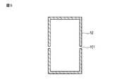
図4は、ブラックマトリクスBMの一例を示す平面図である。この図4は、対向基板6の裏面側の平面パターンを表している。 FIG. 4 is a plan view showing an example of the black matrix BM. FIG. 4 shows a planar pattern on the back side of the
図5は、共通電極12の一例を示す平面図である。この図5は、共通電極12の裏面側の平面パターンを表している。 FIG. 5 is a plan view showing an example of the
対向基板6の裏面側では、格子状のパターンのブラックマトリクスBMと、格子状であるが一部に切り込み151〜154がある共通電極12とが重ねられる。 On the back surface side of the
共通電極12の複数の切り込み151〜154は、電極13と交差する第2軸方向に形成される。本実施形態において、複数の切り込み151〜154は、平行であるとする。このように、共通電極12が複数の切り込み151〜154によって複数の電極部121〜125に区分けされることによって、静電容量の変化に基づく位置検出が可能になる。複数の電極部121〜125のそれぞれは、共通電極12を区分けすることで形成されるため、共通電極12の全体より小さい格子状となる。 The plurality of
各電極部121〜125は、引き出し線161〜165と接続されている。引き出し線161〜165は、対向基板6の額縁領域の側辺部を渡って下辺部の端子171〜175に接続される。端子171〜175は、例えば、ITO(Indium-Tin Oxide)により形成される。 Each electrode part 121-125 is connected with the lead-out lines 161-165. The lead lines 161 to 165 are connected to
端子171〜175は、例えば金パールなどの金属パール(導通粒子)に基づいて形成されるコンタクトを経由して、アクティブマトリクス基板5の配線と電気的に接続される。これにより、端子171〜175とアクティブマトリクス基板5の配線との間で導通を確保することができる。 The
上記の図5の共通電極12は、上記の図4のブラックマトリクスBMと重なるため、共通電極12の切り込み151〜154は、表面側の観察者から視認されることはない。 Since the
図6は、切り込み151を持つ共通電極12の1画素単位の一例を示す平面図である。 FIG. 6 is a plan view showing an example of one pixel unit of the
切れ込み151の幅又は位置によっては表示品質が低下する。しかしながら、例えば、2〜6マイクロメートル、より好ましくは4マイクロメートル程度の幅の切り込み151を、サブピクセルの中央を通るように形成することにより、表示品質の低下を防止することができる。 Depending on the width or position of the
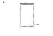
図7は、ブラックマトリクスBMの1画素単位の一例を示す平面図である。 FIG. 7 is a plan view showing an example of one pixel unit of the black matrix BM.
上述したように、このブラックマトリクスBMの1枠は、共通電極12の1枠と重なり、サブピクセルに対応する。 As described above, one frame of the black matrix BM overlaps with one frame of the
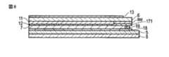
図8は、共通電極12からの引き出し線161の終端の端子171と、アクティブマトリクス基板5の表面側に形成された配線又は端子18との接続状態の一例を示す断面図である。 FIG. 8 is a cross-sectional view showing an example of a connection state between the terminal 171 at the end of the
共通電極12からの引き出し線161の端子171と、アクティブマトリクス基板5の端子18とは、例えば金属パール19などの導通粒子により電気的に接続されている。接続する際に、金属パール19は、例えば直径が10%程度つぶされ、これにより接触面積が増加され、接触抵抗を数十Ωで安定させることができる。 The
本実施形態では、共通電極12をフレキシブルプリント基板とを対向基板6側で接続する必要がなく、低コスト化される。 In this embodiment, it is not necessary to connect the
図9は、電極13の一例を示す平面図である。 FIG. 9 is a plan view showing an example of the
複数の透明電極13は、第1軸方向に長軸を持つストライプ状の透明電極である。複数の透明電極13は、平行である。引き出し線20の一端は透明電極13と電気的に接続されている。引き出し線20の他端は、異方性導電フィルムなどによりフレキシブルプリント基板21と電気的に接続されている。 The plurality of
本実施形態において、液晶表示装置1は、表示信号に基づく駆動と位置検出信号に基づく駆動とを時分割で実行する。透明電極13の時定数は、検出精度及び対応サイズに影響を与える。 In the present embodiment, the liquid
以上説明した本実施形態においては、共通電極12がブラックマトリクスBMと重なるように格子状に形成される。例えば、共通電極12はメタル電極とすることができる。 In the present embodiment described above, the
本実施形態においては、透明電極13が指に近い位置に形成されるため、タッチセンサとしての感度を上げることができる。 In the present embodiment, since the
したがって、本実施形態においては、表示品質を低下させることなく、共通電極12の抵抗値を低くすることができ、低コストで、薄く、軽量で、高感度のインセル型タッチパネル機能を実現することができる。 Therefore, in this embodiment, the resistance value of the
本実施形態においては、共通電極12に切り込み151〜154が形成される。これにより、共通電極12をタッチパネルの送信電極として用いることができ、厚さを薄くすることができ、軽量化することができ、低コスト化することができる。 In the present embodiment,
より詳しく説明すると、本実施形態において、共通電極12と透明電極13とは、誘電体を挟み、一方の電極がタッチパネルの受信電極、他方の電極がタッチパネルの送信電極となり、投影型の静電容量タッチパネルを形成することができる。 More specifically, in the present embodiment, the
さらに、本実施形態においては、共通電極12がブラックマトリクスBMと重なっているため、共通電極12をメタル材で形成しても透過率及び反射などの光学特性に影響を及ぼすことがなく、共通電極12の時定数を下げることができる。 Furthermore, in the present embodiment, since the
さらに、本実施形態に係る液晶表示装置1は、位置検出信号に基づく駆動と表示信号に基づく駆動を時分割で実行するため、共通電極12の時定数を下げることにより低コストで高精度のタッチセンサ機能を実現することができる。 Furthermore, since the liquid
本実施形態は、例として提示したものであり、発明の範囲を限定することは意図していない。この新規な実施形態は、その他の様々な形態で実施されることが可能であり、発明の要旨を逸脱しない範囲で、種々の省略、置き換え、変更を行うことができる。本実施形態やその変形は、発明の範囲や要旨に含まれるとともに、特許請求の範囲に記載された発明とその均等の範囲に含まれる。 This embodiment is presented as an example and is not intended to limit the scope of the invention. The novel embodiment can be implemented in various other forms, and various omissions, replacements, and changes can be made without departing from the scope of the invention. This embodiment and its modifications are included in the scope and gist of the invention, and are included in the invention described in the claims and the equivalents thereof.
1…液晶表示装置、2…照明ユニット、3…液晶表示パネル、4…保護カバー、5…アクティブマトリクス基板、6…対向基板、7…液晶層、8,9…偏光板、10,14,21…フレキシブルプリント基板、11…カラーフィルタ層、12…共通電極、121〜125…電極部、13…透明電極、R…赤フィルタ、G…緑フィルタ、B…青フィルタ、BM…ブラックマトリクス、151〜154…切り込み、161〜164,20…引き出し線、171〜175…端子、19…金属パール。 DESCRIPTION OF
Claims (4)
Translated fromJapanese前記アクティブマトリクス基板に対向する対向基板と、
前記アクティブマトリクス基板と前記対向基板との間に挟まれる液晶層と
を具備し、
前記対向基板は、前記液晶層側から順に、共通電極、カラーフィルタとブラックマトリクスとを含むカラーフィルタ層、及び、静電容量式タッチパネルの一方の電極を備え、
前記共通電極は、前記静電容量式タッチパネルの他方の電極として用いられるメタル電極である送信電極であり、第1の方向に伸びた隣接する複数の前記メタル電極が束ねられてなる電極部が前記第1の方向と交差する第2の方向で分離され、
前記一方の電極は受信電極であり、前記第2の方向に伸びる複数の透明電極を含み、前記共通電極は、隣接する前記メタル電極が束ねられてなる電極部が前記第2の方向で対向する部分では、前記第1の方向に延びた前記メタル電極から複数の前記メタル電極が前記第2の方向に分離し、前記カラーフィルタは前記ブラックマトリクスと前記共通電極との積層構造により囲まれていることを特徴とするタッチパネル機能内蔵液晶表示装置。An active matrix substrate comprising an electronic circuit and wiring connected to the electronic circuit;
A counter substrate facing the active matrix substrate;
A liquid crystal layer sandwiched between the active matrix substrate and the counter substrate;
The counter substrate includes, in order from the liquid crystal layer side, a common electrode, a color filter layer including a color filter and a black matrix, and one electrode of a capacitive touch panel,
The common electrode is a transmission electrode which is a metal electrode used as the other electrode of the capacitive touch panel, and an electrode portion formed by bundling a plurality of adjacent metal electrodes extending in a first direction is Separated in a second direction intersecting the first direction;
The one electrode is a receiving electrode and includes a plurality of transparent electrodes extending in the second direction, and the common electrode has an electrode portion formed by bundling adjacent metal electrodes facing each other in the second direction. In the portion, a plurality of the metal electrodes are separated from the metal electrode extending in the first direction in the second direction, andthe color filter is surrounded by a laminated structure of the black matrix and the common electrode . A liquid crystal display device with a built-in touch panel function.
前記対向基板の表面側には前記一方の電極が形成され、前記対向基板の裏面側には前記共通電極が形成されることを特徴とするタッチパネル機能内蔵液晶表示装置。The liquid crystal display device with a built-in touch panel function according to claim 1,
A liquid crystal display device with a built-in touch panel function, wherein the one electrode is formed on a front surface side of the counter substrate, and the common electrode is formed on a back surface side of the counter substrate.
前記共通電極は前記アクティブマトリクス基板の配線と電気的に接続されることを特徴とするタッチパネル機能内蔵液晶表示装置。The liquid crystal display device with a built-in touch panel function according to claim 1,
The liquid crystal display device with a built-in touch panel function, wherein the common electrode is electrically connected to the wiring of the active matrix substrate.
表示信号に基づく駆動と位置検出信号に基づく駆動とを時分割で行うことを特徴とするタッチパネル機能内蔵液晶表示装置。The liquid crystal display device with a built-in touch panel function according to claim 1,
A liquid crystal display device with a built-in touch panel function, wherein driving based on a display signal and driving based on a position detection signal are performed in a time-sharing manner.
Priority Applications (1)
| Application Number | Priority Date | Filing Date | Title |
|---|---|---|---|
| JP2017229390AJP6588957B2 (en) | 2017-11-29 | 2017-11-29 | LCD device with built-in touch panel function |
Applications Claiming Priority (1)
| Application Number | Priority Date | Filing Date | Title |
|---|---|---|---|
| JP2017229390AJP6588957B2 (en) | 2017-11-29 | 2017-11-29 | LCD device with built-in touch panel function |
Related Parent Applications (1)
| Application Number | Title | Priority Date | Filing Date |
|---|---|---|---|
| JP2013212804ADivisionJP6254812B2 (en) | 2013-10-10 | 2013-10-10 | LCD device with built-in touch panel function |
Publications (2)
| Publication Number | Publication Date |
|---|---|
| JP2018041501A JP2018041501A (en) | 2018-03-15 |
| JP6588957B2true JP6588957B2 (en) | 2019-10-09 |
Family
ID=61626373
Family Applications (1)
| Application Number | Title | Priority Date | Filing Date |
|---|---|---|---|
| JP2017229390AActiveJP6588957B2 (en) | 2017-11-29 | 2017-11-29 | LCD device with built-in touch panel function |
Country Status (1)
| Country | Link |
|---|---|
| JP (1) | JP6588957B2 (en) |
Family Cites Families (4)
| Publication number | Priority date | Publication date | Assignee | Title |
|---|---|---|---|---|
| JP5722573B2 (en)* | 2010-08-24 | 2015-05-20 | 株式会社ジャパンディスプレイ | Display device with touch detection function |
| JP5653686B2 (en)* | 2010-08-24 | 2015-01-14 | 株式会社ジャパンディスプレイ | Display device with touch detection function |
| US8804056B2 (en)* | 2010-12-22 | 2014-08-12 | Apple Inc. | Integrated touch screens |
| JP2012198740A (en)* | 2011-03-22 | 2012-10-18 | Panasonic Corp | Touch panel and display device including touch panel |
- 2017
- 2017-11-29JPJP2017229390Apatent/JP6588957B2/enactiveActive
Also Published As
| Publication number | Publication date |
|---|---|
| JP2018041501A (en) | 2018-03-15 |
Similar Documents
| Publication | Publication Date | Title |
|---|---|---|
| KR102373330B1 (en) | Display device and driving method thereof | |
| TWI764071B (en) | Touch sensor module, window stack structure including the same and image display device including the same | |
| US10203537B2 (en) | Electronic component and electronic device using the same | |
| US9429988B2 (en) | Touch screen panel | |
| JP5970805B2 (en) | Touch panel sensor with transparent sheet | |
| US11042237B2 (en) | Display device | |
| TWI502445B (en) | Touch display device and touch substrate | |
| JP2015056470A (en) | Organic electroluminescence device with input function | |
| JP2014211825A (en) | Display device | |
| CN204883640U (en) | Sensor device and display device | |
| JP6539214B2 (en) | Display with sensor | |
| US11605679B2 (en) | Display device | |
| US9529462B2 (en) | Touch panel | |
| JP6254812B2 (en) | LCD device with built-in touch panel function | |
| JP2014222438A (en) | Electronic component and electronic apparatus | |
| JP6588957B2 (en) | LCD device with built-in touch panel function | |
| US11880520B2 (en) | Display device | |
| CN115084174B (en) | Detection device and display device | |
| US10521037B2 (en) | Display panel with touch sensor | |
| CN112181198B (en) | Touch module and electronic equipment | |
| JP6797970B2 (en) | Display device | |
| US11307716B2 (en) | Capacitive touch glass structure | |
| WO2024185379A1 (en) | Touch panel | |
| JP2022089855A (en) | Display | |
| KR20240029681A (en) | Display device |
Legal Events
| Date | Code | Title | Description |
|---|---|---|---|
| A621 | Written request for application examination | Free format text:JAPANESE INTERMEDIATE CODE: A621 Effective date:20171129 | |
| A131 | Notification of reasons for refusal | Free format text:JAPANESE INTERMEDIATE CODE: A131 Effective date:20180724 | |
| A977 | Report on retrieval | Free format text:JAPANESE INTERMEDIATE CODE: A971007 Effective date:20180725 | |
| A521 | Request for written amendment filed | Free format text:JAPANESE INTERMEDIATE CODE: A523 Effective date:20180913 | |
| A131 | Notification of reasons for refusal | Free format text:JAPANESE INTERMEDIATE CODE: A131 Effective date:20190226 | |
| A521 | Request for written amendment filed | Free format text:JAPANESE INTERMEDIATE CODE: A523 Effective date:20190422 | |
| TRDD | Decision of grant or rejection written | ||
| A01 | Written decision to grant a patent or to grant a registration (utility model) | Free format text:JAPANESE INTERMEDIATE CODE: A01 Effective date:20190903 | |
| A61 | First payment of annual fees (during grant procedure) | Free format text:JAPANESE INTERMEDIATE CODE: A61 Effective date:20190913 | |
| R150 | Certificate of patent or registration of utility model | Ref document number:6588957 Country of ref document:JP Free format text:JAPANESE INTERMEDIATE CODE: R150 | |
| R250 | Receipt of annual fees | Free format text:JAPANESE INTERMEDIATE CODE: R250 | |
| R250 | Receipt of annual fees | Free format text:JAPANESE INTERMEDIATE CODE: R250 | |
| R250 | Receipt of annual fees | Free format text:JAPANESE INTERMEDIATE CODE: R250 | |
| S111 | Request for change of ownership or part of ownership | Free format text:JAPANESE INTERMEDIATE CODE: R313113 | |
| R350 | Written notification of registration of transfer | Free format text:JAPANESE INTERMEDIATE CODE: R350 | |
| R250 | Receipt of annual fees | Free format text:JAPANESE INTERMEDIATE CODE: R250 |