JP6584347B2 - Deposition method - Google Patents
Deposition methodDownload PDFInfo
- Publication number
- JP6584347B2 JP6584347B2JP2016040217AJP2016040217AJP6584347B2JP 6584347 B2JP6584347 B2JP 6584347B2JP 2016040217 AJP2016040217 AJP 2016040217AJP 2016040217 AJP2016040217 AJP 2016040217AJP 6584347 B2JP6584347 B2JP 6584347B2
- Authority
- JP
- Japan
- Prior art keywords
- gas
- plasma
- film
- substrate
- turntable
- Prior art date
- Legal status (The legal status is an assumption and is not a legal conclusion. Google has not performed a legal analysis and makes no representation as to the accuracy of the status listed.)
- Active
Links
Images


Classifications
- H—ELECTRICITY
- H01—ELECTRIC ELEMENTS
- H01L—SEMICONDUCTOR DEVICES NOT COVERED BY CLASS H10
- H01L21/00—Processes or apparatus adapted for the manufacture or treatment of semiconductor or solid state devices or of parts thereof
- H01L21/02—Manufacture or treatment of semiconductor devices or of parts thereof
- H01L21/02104—Forming layers
- H01L21/02107—Forming insulating materials on a substrate
- H01L21/02225—Forming insulating materials on a substrate characterised by the process for the formation of the insulating layer
- H01L21/0226—Forming insulating materials on a substrate characterised by the process for the formation of the insulating layer formation by a deposition process
- H01L21/02263—Forming insulating materials on a substrate characterised by the process for the formation of the insulating layer formation by a deposition process deposition from the gas or vapour phase
- H01L21/02271—Forming insulating materials on a substrate characterised by the process for the formation of the insulating layer formation by a deposition process deposition from the gas or vapour phase deposition by decomposition or reaction of gaseous or vapour phase compounds, i.e. chemical vapour deposition
- H01L21/02274—Forming insulating materials on a substrate characterised by the process for the formation of the insulating layer formation by a deposition process deposition from the gas or vapour phase deposition by decomposition or reaction of gaseous or vapour phase compounds, i.e. chemical vapour deposition in the presence of a plasma [PECVD]
- C—CHEMISTRY; METALLURGY
- C23—COATING METALLIC MATERIAL; COATING MATERIAL WITH METALLIC MATERIAL; CHEMICAL SURFACE TREATMENT; DIFFUSION TREATMENT OF METALLIC MATERIAL; COATING BY VACUUM EVAPORATION, BY SPUTTERING, BY ION IMPLANTATION OR BY CHEMICAL VAPOUR DEPOSITION, IN GENERAL; INHIBITING CORROSION OF METALLIC MATERIAL OR INCRUSTATION IN GENERAL
- C23C—COATING METALLIC MATERIAL; COATING MATERIAL WITH METALLIC MATERIAL; SURFACE TREATMENT OF METALLIC MATERIAL BY DIFFUSION INTO THE SURFACE, BY CHEMICAL CONVERSION OR SUBSTITUTION; COATING BY VACUUM EVAPORATION, BY SPUTTERING, BY ION IMPLANTATION OR BY CHEMICAL VAPOUR DEPOSITION, IN GENERAL
- C23C16/00—Chemical coating by decomposition of gaseous compounds, without leaving reaction products of surface material in the coating, i.e. chemical vapour deposition [CVD] processes
- C23C16/22—Chemical coating by decomposition of gaseous compounds, without leaving reaction products of surface material in the coating, i.e. chemical vapour deposition [CVD] processes characterised by the deposition of inorganic material, other than metallic material
- C23C16/30—Deposition of compounds, mixtures or solid solutions, e.g. borides, carbides, nitrides
- C23C16/34—Nitrides
- C23C16/345—Silicon nitride
- C—CHEMISTRY; METALLURGY
- C23—COATING METALLIC MATERIAL; COATING MATERIAL WITH METALLIC MATERIAL; CHEMICAL SURFACE TREATMENT; DIFFUSION TREATMENT OF METALLIC MATERIAL; COATING BY VACUUM EVAPORATION, BY SPUTTERING, BY ION IMPLANTATION OR BY CHEMICAL VAPOUR DEPOSITION, IN GENERAL; INHIBITING CORROSION OF METALLIC MATERIAL OR INCRUSTATION IN GENERAL
- C23C—COATING METALLIC MATERIAL; COATING MATERIAL WITH METALLIC MATERIAL; SURFACE TREATMENT OF METALLIC MATERIAL BY DIFFUSION INTO THE SURFACE, BY CHEMICAL CONVERSION OR SUBSTITUTION; COATING BY VACUUM EVAPORATION, BY SPUTTERING, BY ION IMPLANTATION OR BY CHEMICAL VAPOUR DEPOSITION, IN GENERAL
- C23C16/00—Chemical coating by decomposition of gaseous compounds, without leaving reaction products of surface material in the coating, i.e. chemical vapour deposition [CVD] processes
- C23C16/22—Chemical coating by decomposition of gaseous compounds, without leaving reaction products of surface material in the coating, i.e. chemical vapour deposition [CVD] processes characterised by the deposition of inorganic material, other than metallic material
- C23C16/24—Deposition of silicon only
- C—CHEMISTRY; METALLURGY
- C23—COATING METALLIC MATERIAL; COATING MATERIAL WITH METALLIC MATERIAL; CHEMICAL SURFACE TREATMENT; DIFFUSION TREATMENT OF METALLIC MATERIAL; COATING BY VACUUM EVAPORATION, BY SPUTTERING, BY ION IMPLANTATION OR BY CHEMICAL VAPOUR DEPOSITION, IN GENERAL; INHIBITING CORROSION OF METALLIC MATERIAL OR INCRUSTATION IN GENERAL
- C23C—COATING METALLIC MATERIAL; COATING MATERIAL WITH METALLIC MATERIAL; SURFACE TREATMENT OF METALLIC MATERIAL BY DIFFUSION INTO THE SURFACE, BY CHEMICAL CONVERSION OR SUBSTITUTION; COATING BY VACUUM EVAPORATION, BY SPUTTERING, BY ION IMPLANTATION OR BY CHEMICAL VAPOUR DEPOSITION, IN GENERAL
- C23C16/00—Chemical coating by decomposition of gaseous compounds, without leaving reaction products of surface material in the coating, i.e. chemical vapour deposition [CVD] processes
- C23C16/44—Chemical coating by decomposition of gaseous compounds, without leaving reaction products of surface material in the coating, i.e. chemical vapour deposition [CVD] processes characterised by the method of coating
- C23C16/455—Chemical coating by decomposition of gaseous compounds, without leaving reaction products of surface material in the coating, i.e. chemical vapour deposition [CVD] processes characterised by the method of coating characterised by the method used for introducing gases into reaction chamber or for modifying gas flows in reaction chamber
- C23C16/45523—Pulsed gas flow or change of composition over time
- C23C16/45525—Atomic layer deposition [ALD]
- C23C16/45527—Atomic layer deposition [ALD] characterized by the ALD cycle, e.g. different flows or temperatures during half-reactions, unusual pulsing sequence, use of precursor mixtures or auxiliary reactants or activations
- C23C16/45536—Use of plasma, radiation or electromagnetic fields
- C23C16/4554—Plasma being used non-continuously in between ALD reactions
- C—CHEMISTRY; METALLURGY
- C23—COATING METALLIC MATERIAL; COATING MATERIAL WITH METALLIC MATERIAL; CHEMICAL SURFACE TREATMENT; DIFFUSION TREATMENT OF METALLIC MATERIAL; COATING BY VACUUM EVAPORATION, BY SPUTTERING, BY ION IMPLANTATION OR BY CHEMICAL VAPOUR DEPOSITION, IN GENERAL; INHIBITING CORROSION OF METALLIC MATERIAL OR INCRUSTATION IN GENERAL
- C23C—COATING METALLIC MATERIAL; COATING MATERIAL WITH METALLIC MATERIAL; SURFACE TREATMENT OF METALLIC MATERIAL BY DIFFUSION INTO THE SURFACE, BY CHEMICAL CONVERSION OR SUBSTITUTION; COATING BY VACUUM EVAPORATION, BY SPUTTERING, BY ION IMPLANTATION OR BY CHEMICAL VAPOUR DEPOSITION, IN GENERAL
- C23C16/00—Chemical coating by decomposition of gaseous compounds, without leaving reaction products of surface material in the coating, i.e. chemical vapour deposition [CVD] processes
- C23C16/44—Chemical coating by decomposition of gaseous compounds, without leaving reaction products of surface material in the coating, i.e. chemical vapour deposition [CVD] processes characterised by the method of coating
- C23C16/455—Chemical coating by decomposition of gaseous compounds, without leaving reaction products of surface material in the coating, i.e. chemical vapour deposition [CVD] processes characterised by the method of coating characterised by the method used for introducing gases into reaction chamber or for modifying gas flows in reaction chamber
- C23C16/45523—Pulsed gas flow or change of composition over time
- C23C16/45525—Atomic layer deposition [ALD]
- C23C16/45527—Atomic layer deposition [ALD] characterized by the ALD cycle, e.g. different flows or temperatures during half-reactions, unusual pulsing sequence, use of precursor mixtures or auxiliary reactants or activations
- C23C16/45536—Use of plasma, radiation or electromagnetic fields
- C23C16/45542—Plasma being used non-continuously during the ALD reactions
- C—CHEMISTRY; METALLURGY
- C23—COATING METALLIC MATERIAL; COATING MATERIAL WITH METALLIC MATERIAL; CHEMICAL SURFACE TREATMENT; DIFFUSION TREATMENT OF METALLIC MATERIAL; COATING BY VACUUM EVAPORATION, BY SPUTTERING, BY ION IMPLANTATION OR BY CHEMICAL VAPOUR DEPOSITION, IN GENERAL; INHIBITING CORROSION OF METALLIC MATERIAL OR INCRUSTATION IN GENERAL
- C23C—COATING METALLIC MATERIAL; COATING MATERIAL WITH METALLIC MATERIAL; SURFACE TREATMENT OF METALLIC MATERIAL BY DIFFUSION INTO THE SURFACE, BY CHEMICAL CONVERSION OR SUBSTITUTION; COATING BY VACUUM EVAPORATION, BY SPUTTERING, BY ION IMPLANTATION OR BY CHEMICAL VAPOUR DEPOSITION, IN GENERAL
- C23C16/00—Chemical coating by decomposition of gaseous compounds, without leaving reaction products of surface material in the coating, i.e. chemical vapour deposition [CVD] processes
- C23C16/44—Chemical coating by decomposition of gaseous compounds, without leaving reaction products of surface material in the coating, i.e. chemical vapour deposition [CVD] processes characterised by the method of coating
- C23C16/455—Chemical coating by decomposition of gaseous compounds, without leaving reaction products of surface material in the coating, i.e. chemical vapour deposition [CVD] processes characterised by the method of coating characterised by the method used for introducing gases into reaction chamber or for modifying gas flows in reaction chamber
- C23C16/45523—Pulsed gas flow or change of composition over time
- C23C16/45525—Atomic layer deposition [ALD]
- C23C16/45544—Atomic layer deposition [ALD] characterized by the apparatus
- C23C16/45548—Atomic layer deposition [ALD] characterized by the apparatus having arrangements for gas injection at different locations of the reactor for each ALD half-reaction
- C23C16/45551—Atomic layer deposition [ALD] characterized by the apparatus having arrangements for gas injection at different locations of the reactor for each ALD half-reaction for relative movement of the substrate and the gas injectors or half-reaction reactor compartments
- C—CHEMISTRY; METALLURGY
- C23—COATING METALLIC MATERIAL; COATING MATERIAL WITH METALLIC MATERIAL; CHEMICAL SURFACE TREATMENT; DIFFUSION TREATMENT OF METALLIC MATERIAL; COATING BY VACUUM EVAPORATION, BY SPUTTERING, BY ION IMPLANTATION OR BY CHEMICAL VAPOUR DEPOSITION, IN GENERAL; INHIBITING CORROSION OF METALLIC MATERIAL OR INCRUSTATION IN GENERAL
- C23C—COATING METALLIC MATERIAL; COATING MATERIAL WITH METALLIC MATERIAL; SURFACE TREATMENT OF METALLIC MATERIAL BY DIFFUSION INTO THE SURFACE, BY CHEMICAL CONVERSION OR SUBSTITUTION; COATING BY VACUUM EVAPORATION, BY SPUTTERING, BY ION IMPLANTATION OR BY CHEMICAL VAPOUR DEPOSITION, IN GENERAL
- C23C16/00—Chemical coating by decomposition of gaseous compounds, without leaving reaction products of surface material in the coating, i.e. chemical vapour deposition [CVD] processes
- C23C16/44—Chemical coating by decomposition of gaseous compounds, without leaving reaction products of surface material in the coating, i.e. chemical vapour deposition [CVD] processes characterised by the method of coating
- C23C16/50—Chemical coating by decomposition of gaseous compounds, without leaving reaction products of surface material in the coating, i.e. chemical vapour deposition [CVD] processes characterised by the method of coating using electric discharges
- H—ELECTRICITY
- H01—ELECTRIC ELEMENTS
- H01J—ELECTRIC DISCHARGE TUBES OR DISCHARGE LAMPS
- H01J37/00—Discharge tubes with provision for introducing objects or material to be exposed to the discharge, e.g. for the purpose of examination or processing thereof
- H01J37/32—Gas-filled discharge tubes
- H01J37/32009—Arrangements for generation of plasma specially adapted for examination or treatment of objects, e.g. plasma sources
- H01J37/32082—Radio frequency generated discharge
- H01J37/321—Radio frequency generated discharge the radio frequency energy being inductively coupled to the plasma
- H01J37/3211—Antennas, e.g. particular shapes of coils
- H—ELECTRICITY
- H01—ELECTRIC ELEMENTS
- H01J—ELECTRIC DISCHARGE TUBES OR DISCHARGE LAMPS
- H01J37/00—Discharge tubes with provision for introducing objects or material to be exposed to the discharge, e.g. for the purpose of examination or processing thereof
- H01J37/32—Gas-filled discharge tubes
- H01J37/32009—Arrangements for generation of plasma specially adapted for examination or treatment of objects, e.g. plasma sources
- H01J37/32082—Radio frequency generated discharge
- H01J37/321—Radio frequency generated discharge the radio frequency energy being inductively coupled to the plasma
- H01J37/32119—Windows
- H—ELECTRICITY
- H01—ELECTRIC ELEMENTS
- H01J—ELECTRIC DISCHARGE TUBES OR DISCHARGE LAMPS
- H01J37/00—Discharge tubes with provision for introducing objects or material to be exposed to the discharge, e.g. for the purpose of examination or processing thereof
- H01J37/32—Gas-filled discharge tubes
- H01J37/32431—Constructional details of the reactor
- H01J37/32458—Vessel
- H01J37/32513—Sealing means, e.g. sealing between different parts of the vessel
- H—ELECTRICITY
- H01—ELECTRIC ELEMENTS
- H01J—ELECTRIC DISCHARGE TUBES OR DISCHARGE LAMPS
- H01J37/00—Discharge tubes with provision for introducing objects or material to be exposed to the discharge, e.g. for the purpose of examination or processing thereof
- H01J37/32—Gas-filled discharge tubes
- H01J37/32431—Constructional details of the reactor
- H01J37/32733—Means for moving the material to be treated
- H01J37/32752—Means for moving the material to be treated for moving the material across the discharge
- H—ELECTRICITY
- H01—ELECTRIC ELEMENTS
- H01L—SEMICONDUCTOR DEVICES NOT COVERED BY CLASS H10
- H01L21/00—Processes or apparatus adapted for the manufacture or treatment of semiconductor or solid state devices or of parts thereof
- H01L21/02—Manufacture or treatment of semiconductor devices or of parts thereof
- H01L21/02041—Cleaning
- H01L21/02043—Cleaning before device manufacture, i.e. Begin-Of-Line process
- H01L21/02046—Dry cleaning only
- H—ELECTRICITY
- H01—ELECTRIC ELEMENTS
- H01L—SEMICONDUCTOR DEVICES NOT COVERED BY CLASS H10
- H01L21/00—Processes or apparatus adapted for the manufacture or treatment of semiconductor or solid state devices or of parts thereof
- H01L21/02—Manufacture or treatment of semiconductor devices or of parts thereof
- H01L21/02104—Forming layers
- H01L21/02107—Forming insulating materials on a substrate
- H01L21/02109—Forming insulating materials on a substrate characterised by the type of layer, e.g. type of material, porous/non-porous, pre-cursors, mixtures or laminates
- H01L21/02112—Forming insulating materials on a substrate characterised by the type of layer, e.g. type of material, porous/non-porous, pre-cursors, mixtures or laminates characterised by the material of the layer
- H01L21/02123—Forming insulating materials on a substrate characterised by the type of layer, e.g. type of material, porous/non-porous, pre-cursors, mixtures or laminates characterised by the material of the layer the material containing silicon
- H01L21/0217—Forming insulating materials on a substrate characterised by the type of layer, e.g. type of material, porous/non-porous, pre-cursors, mixtures or laminates characterised by the material of the layer the material containing silicon the material being a silicon nitride not containing oxygen, e.g. SixNy or SixByNz
- H—ELECTRICITY
- H01—ELECTRIC ELEMENTS
- H01L—SEMICONDUCTOR DEVICES NOT COVERED BY CLASS H10
- H01L21/00—Processes or apparatus adapted for the manufacture or treatment of semiconductor or solid state devices or of parts thereof
- H01L21/02—Manufacture or treatment of semiconductor devices or of parts thereof
- H01L21/02104—Forming layers
- H01L21/02107—Forming insulating materials on a substrate
- H01L21/02296—Forming insulating materials on a substrate characterised by the treatment performed before or after the formation of the layer
- H01L21/02299—Forming insulating materials on a substrate characterised by the treatment performed before or after the formation of the layer pre-treatment
- H01L21/02312—Forming insulating materials on a substrate characterised by the treatment performed before or after the formation of the layer pre-treatment treatment by exposure to a gas or vapour
- H01L21/02315—Forming insulating materials on a substrate characterised by the treatment performed before or after the formation of the layer pre-treatment treatment by exposure to a gas or vapour treatment by exposure to a plasma
- H—ELECTRICITY
- H01—ELECTRIC ELEMENTS
- H01L—SEMICONDUCTOR DEVICES NOT COVERED BY CLASS H10
- H01L21/00—Processes or apparatus adapted for the manufacture or treatment of semiconductor or solid state devices or of parts thereof
- H01L21/02—Manufacture or treatment of semiconductor devices or of parts thereof
- H01L21/02104—Forming layers
- H01L21/02365—Forming inorganic semiconducting materials on a substrate
- H01L21/02518—Deposited layers
- H01L21/02521—Materials
- H01L21/02538—Group 13/15 materials
- H01L21/0254—Nitrides
- H—ELECTRICITY
- H01—ELECTRIC ELEMENTS
- H01L—SEMICONDUCTOR DEVICES NOT COVERED BY CLASS H10
- H01L21/00—Processes or apparatus adapted for the manufacture or treatment of semiconductor or solid state devices or of parts thereof
- H01L21/02—Manufacture or treatment of semiconductor devices or of parts thereof
- H01L21/02104—Forming layers
- H01L21/02365—Forming inorganic semiconducting materials on a substrate
- H01L21/02612—Formation types
- H01L21/02617—Deposition types
- H01L21/0262—Reduction or decomposition of gaseous compounds, e.g. CVD
Landscapes
- Chemical & Material Sciences (AREA)
- Engineering & Computer Science (AREA)
- Physics & Mathematics (AREA)
- Plasma & Fusion (AREA)
- Chemical Kinetics & Catalysis (AREA)
- Mechanical Engineering (AREA)
- Organic Chemistry (AREA)
- Materials Engineering (AREA)
- Metallurgy (AREA)
- General Chemical & Material Sciences (AREA)
- Analytical Chemistry (AREA)
- Microelectronics & Electronic Packaging (AREA)
- Power Engineering (AREA)
- Condensed Matter Physics & Semiconductors (AREA)
- General Physics & Mathematics (AREA)
- Manufacturing & Machinery (AREA)
- Computer Hardware Design (AREA)
- Electromagnetism (AREA)
- Inorganic Chemistry (AREA)
- Chemical Vapour Deposition (AREA)
- Formation Of Insulating Films (AREA)
Description
Translated fromJapanese本発明は、成膜方法に関する。 The present invention relates to a film forming method.
従来から、ALD(Atomic Layer Deposition、原子層堆積法)を用いた成膜方法において、2個のプラズマ発生手段を搭載した成膜装置を用いて成膜を行う成膜方法が知られている(例えば、特許文献1参照)。 2. Description of the Related Art Conventionally, in a film forming method using ALD (Atomic Layer Deposition), a film forming method for forming a film using a film forming apparatus equipped with two plasma generating means is known ( For example, see Patent Document 1).
かかる特許文献1に記載の成膜装置は、真空容器内に回転テーブルを有し、回転テーブル上に基板を載置可能に構成されている。そして、成膜装置は、基板の表面に第1の処理ガスを供給する第1の処理ガス供給手段と、第1のプラズマ処理用ガスを供給する第1のプラズマ処理用ガス供給手段と、第2のプラズマ処理用ガスを供給する第2のプラズマ処理用ガス供給手段とを備える。更に、成膜装置は、第1のプラズマ処理用ガスをプラズマ化する第1のプラズマ発生手段と、第2のプラズマ処理用ガスをプラズマ化する第2のプラズマ発生手段とを備え、第2のプラズマ発生手段と回転テーブルとの距離は、第1のプラズマ発生手段と回転テーブルとの距離よりも短く設定されている。これにより、第2のプラズマ処理用ガスのイオンエネルギー及びラジカル濃度を、第1のプラズマ処理用ガスのイオンエネルギー及びラジカル濃度より高くすることができる。 The film forming apparatus described in
かかる構造を有する成膜装置を用いて、第1の処理ガス供給手段からシリコン含有ガス、第1のプラズマ処理用ガス供給手段からNH3、第2のプラズマ処理用ガス供給手段からNH3/Ar/H2の混合ガスを供給することにより、基板に吸着したシリコン含有ガスをイオンエネルギー及びラジカル濃度が低いNH3により窒化し、次いでイオンエネルギー及びラジカル濃度が低いNH3/Ar/H2の混合ガスで改質処理を行うことができ、パターンの表面積に依存して面内成膜量が変化する所謂ローディング効果を抑制することができる。Using the film forming apparatus having such a structure, the silicon-containing gas is supplied from the first processing gas supply means, NH3 is supplied from the first plasma processing gas supply means, and NH3 / Ar is supplied from the second plasma processing gas supply means. By supplying a mixed gas of / H2 , the silicon-containing gas adsorbed on the substrate is nitrided with NH3 having a low ion energy and radical concentration, and then mixed with NH3 / Ar / H2 having a low ion energy and radical concentration. The reforming process can be performed with a gas, and the so-called loading effect in which the in-plane deposition amount changes depending on the surface area of the pattern can be suppressed.
しかしながら、上述の特許文献1に記載の成膜方法を用いた場合であっても、回転テーブルの半径方向における基板の端部の成膜が不十分な場合があり、更なる面内均一性の向上が求められる場合がある。 However, even when the film forming method described in
そこで、本発明は、面内均一性を高めることができる成膜方法を提供することを目的とする。 Therefore, an object of the present invention is to provide a film forming method that can improve in-plane uniformity.
上記目的を達成するため、本発明の一態様に係る成膜方法は、基板の表面にSi含有ガスを供給し、前記基板の前記表面に前記Si含有ガスを吸着させる工程と、
前記基板の表面にパージガスを供給する工程と、
前記基板の前記表面に窒化ガスを第1のプラズマにより活性化して供給し、前記基板の前記表面上に吸着した前記Si含有ガスを窒化し、SiN膜を堆積させる工程と、
前記基板の前記表面にNH3及びN2をN2がNH3の3倍以上の比率で含む改質ガスを第2のプラズマにより活性化して供給し、前記基板の前記表面上に堆積した前記SiN膜を改質する工程と、
前記基板の表面にパージガスを供給する工程と、を有し、
前記基板は、処理室内に設けられた回転テーブルの表面上に周方向に沿って載置され、
前記処理室内の前記回転テーブルの上方には、前記回転テーブルの回転方向に沿って順に配置されたSi含有ガス供給領域、第1のパージガス供給領域、窒化ガス供給領域、改質ガス供給領域及び第2のパージガス供給領域が設けられ、
前記回転テーブルを1回転させることにより、前記基板が前記Si含有ガス供給領域、前記第1のパージガス供給領域、前記窒化ガス供給領域、前記改質ガス供給領域及び前記第2のパージガス供給領域を通過することにより、前記Si含有ガスを吸着させる工程、前記パージガスを供給する工程、前記SiN膜を堆積させる工程、前記SiN膜を改質する工程及び前記パージガスを供給する工程を1サイクル行い、前記回転テーブルを連続的に複数回回転させることにより、前記1サイクルを複数回繰り返す。In order to achieve the above object, a film forming method according to an aspect of the present invention includes a step of supplying a Si-containing gas to a surface of a substrate and adsorbing the Si-containing gas to the surface of the substrate;
Supplying a purge gas to the surface of the substrate;
Activating and supplying a nitriding gas to the surface of the substrate by a first plasma, nitriding the Si-containing gas adsorbed on the surface of the substrate, and depositing a SiN film;
Wherein the NH3 and N2 on the surface of the substrateN2is a reformed gas activated by supplying a second plasma containing atleast three times the ratioofNH3, was deposited on the surface of the substrate A step of modifying theSiN film ;
Havea, a step of supplying a purge gas to the surface of thesubstrate,
The substrate is placed along the circumferential direction on the surface of a turntable provided in the processing chamber,
Above the turntable in the processing chamber, a Si-containing gas supply region, a first purge gas supply region, a nitriding gas supply region, a reformed gas supply region, and a first gas gas are disposed in order along the rotation direction of the turntable. 2 purge gas supply areas are provided,
By rotating the rotary table once, the substrate passes through the Si-containing gas supply region, the first purge gas supply region, the nitriding gas supply region, the reformed gas supply region, and the second purge gas supply region. The step of adsorbing the Si-containing gas, the step of supplying the purge gas, the step of depositing the SiN film, the step of modifying the SiN film, and the step of supplying the purge gas are performed in one cycle, and the rotation The one cycle is repeated a plurality of times by continuously rotating the table a plurality of times .
本発明によれば、面内均一性の高い成膜を行うことができる。 According to the present invention, film formation with high in-plane uniformity can be performed.
以下、図面を参照して、本発明を実施するための形態の説明を行う。 DESCRIPTION OF EMBODIMENTS Hereinafter, embodiments for carrying out the present invention will be described with reference to the drawings.
〔成膜装置の構成〕
図1に、本発明の実施形態に係る成膜方法を実施する成膜装置の一例の概略縦断面図を示す。また、図2に、本発明の実施形態に係る成膜方法を実施する成膜装置の一例の概略平面図を示す。なお、図2では、説明の便宜上、天板11の描画を省略している。[Configuration of deposition system]
FIG. 1 shows a schematic longitudinal sectional view of an example of a film forming apparatus for performing a film forming method according to an embodiment of the present invention. FIG. 2 shows a schematic plan view of an example of a film forming apparatus for performing the film forming method according to the embodiment of the present invention. In FIG. 2, drawing of the
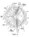
図1に示すように、本発明の実施形態に係る成膜方法を実施する成膜装置は、平面形状が概ね円形である真空容器1と、この真空容器1内に設けられ、真空容器1の中心に回転中心を有すると共にウエハWを公転させるための回転テーブル2と、を備えている。 As shown in FIG. 1, a film forming apparatus that performs a film forming method according to an embodiment of the present invention includes a
真空容器1は、内部で基板を処理するための処理室である。真空容器1は、回転テーブル2の後述する凹部24に対向する位置に設けられた天板(天井部)11と、容器本体12とを備えている。また、容器本体12の上面の周縁部には、リング状に設けられたシール部材13が設けられている。そして、天板11は、容器本体12から着脱可能に構成されている。平面視における真空容器1の直径寸法(内径寸法)は、限定されないが、例えば1100mm程度とすることができる。 The
真空容器1内の上面側における中央部には、真空容器1内の中心部領域Cにおいて互いに異なる処理ガス同士が混ざり合うことを抑制するために分離ガスを供給する、分離ガス供給管51が接続されている。 A separation
回転テーブル2は、中心部にて概略円筒形状のコア部21に固定されており、このコア部21の下面に接続されると共に鉛直方向に伸びる回転軸22に対して、鉛直軸周り、図2に示す例では時計回りに、駆動部23によって回転自在に構成されている。回転テーブル2の直径寸法は、限定されないが、例えば1000mm程度とすることができる。 The rotary table 2 is fixed to a substantially
回転軸22及び駆動部23は、ケース体20に収納されており、このケース体20は、上面側のフランジ部分が真空容器1の底面部14の下面に気密に取り付けられている。また、このケース体20には、回転テーブル2の下方領域に窒素ガス等をパージガス(分離ガス)として供給するためのパージガス供給管72が接続されている。 The rotating
真空容器1の底面部14におけるコア部21の外周側は、回転テーブル2に下方側から近接するようにリング状に形成されて突出部12aを為している。 The outer peripheral side of the
回転テーブル2の表面部には、直径寸法が例えば300mmのウエハWを載置するための円形状の凹部24が基板載置領域として形成されている。この凹部24は、回転テーブル2の回転方向に沿って、複数箇所、例えば5箇所に設けられている。凹部24は、ウエハWの直径よりも僅かに、具体的には1mm乃至4mm程度大きい内径を有する。また、凹部24の深さは、ウエハWの厚さにほぼ等しいか、又はウエハWの厚さよりも大きく構成される。したがって、ウエハWが凹部24に収容されると、ウエハWの表面と、回転テーブル2のウエハWが載置されない領域の表面とが同じ高さになるか、ウエハWの表面が回転テーブル2の表面よりも低くなる。なお、凹部24の深さは、ウエハWの厚さよりも深い場合であっても、あまり深くすると成膜に影響が出ることがあるので、ウエハWの厚さの3倍程度の深さまでとすることが好ましい。 A circular recess 24 for mounting a wafer W having a diameter of, for example, 300 mm is formed on the surface of the
なお、ウエハWの表面には、トレンチ、ビア等の窪みパターンが形成されている。本発明の実施形態に係る成膜方法は、窪みパターン内に埋め込み成膜を行うのに適した方法であるので、表面に窪みパターンが形成されてウエハWの埋め込み成膜に好適に適用され得る。 A recess pattern such as a trench and a via is formed on the surface of the wafer W. Since the film formation method according to the embodiment of the present invention is a method suitable for performing embedded film formation in the recess pattern, the recess pattern is formed on the surface and can be suitably applied to the embedded film formation of the wafer W. .
凹部24の底面には、ウエハWを下方側から突き上げて昇降させるための例えば後述する3本の昇降ピンが貫通する、図示しない貫通孔が形成されている。 A through hole (not shown) through which, for example, three elevating pins to be described later penetrate for raising and lowering the wafer W from below is formed on the bottom surface of the
図2に示すように、回転テーブル2における凹部24の通過領域と対向する位置には、例えば石英からなる複数本、例えば5本のノズル31、32、33、41、42が真空容器1の周方向に互いに間隔をおいて放射状に配置されている。これら各々のノズル31、32、33、41、42は、回転テーブル2と天板11との間に配置される。また、これら各々のノズル31、32、33、41、42は、例えば真空容器1の外周壁から中心部領域Cに向かってウエハWに対向して水平に伸びるように取り付けられている。 As shown in FIG. 2, a plurality of, for example, five
図2に示す例では、原料ガスノズル31から時計回り(回転テーブル2の回転方向)に、分離ガスノズル42、第1のプラズマ処理用ガスノズル32、第2のプラズマ処理用ガスノズル33、分離ガスノズル41がこの順番で配列されている。しかしながら、本実施形態に係る成膜装置は、この形態に限定されず、回転テーブル2の回転方向は反時計回りであっても良く、この場合、原料ガスノズル31から反時計回りに、分離ガスノズル42、第1のプラズマ処理用ガスノズル32、第2のプラズマ処理用ガスノズル33、分離ガスノズル41がこの順番で配列されている。 In the example shown in FIG. 2, the
第1のプラズマ処理用ガスノズル32、第2のプラズマ処理用ガスノズル33の上方側には、図2に示すように、各々のプラズマ処理用ガスノズルから吐出されるガスをプラズマ化するために、プラズマ発生器81a、81bが各々設けられている。これらプラズマ発生器81a、81bについては、後述する。 As shown in FIG. 2, plasma is generated on the upper side of the first plasma
なお、本実施形態においては、各々の処理領域に1つのノズルを配置する例を示したが、各々の処理領域に複数のノズルを配置する構成であっても良い。例えば、第1のプラズマ処理用ガスノズル32は、複数のプラズマ処理用ガスノズルから構成され、各々、後述するアルゴン(Ar)ガス、アンモニア(NH3)ガス、水素(H2)ガス等を供給する構成であっても良いし、1つのプラズマ処理用ガスノズルのみを配置し、アルゴンガス、アンモニアガス及び水素ガスの混合ガスを供給する構成であっても良い。In the present embodiment, an example in which one nozzle is disposed in each processing region has been described, but a configuration in which a plurality of nozzles are disposed in each processing region may be employed. For example, the first plasma
原料ガスノズル31は、原料ガス供給部をなしている。また、第1のプラズマ処理用ガスノズル32は、第1のプラズマ処理用ガス供給部をなしており、第2のプラズマ処理用ガスノズル33は、第2のプラズマ処理用ガス供給部をなしている。さらに、分離ガスノズル41、42は、各々分離ガス供給部をなしている。なお、分離ガスは、上述のように、パージガスと呼んでもよい。 The
各ノズル31、32、33、41、42は、流量調整バルブを介して、図示しない各々のガス供給源に接続されている。 Each
原料ガスノズル31から供給される原料ガスは、シリコン含有ガスである。シリコン含有ガスの一例としては、DCS[ジクロロシラン]、ジシラン(Si2H6)、HCD[ヘキサクロロジシラン]、DIPAS[ジイソプロピルアミノシラン]、3DMAS[トリスジメチルアミノシラン]、BTBAS[ビスターシャルブチルアミノシラン]等のガスが挙げられる。The source gas supplied from the
原料ガスノズル31から供給される原料ガスとして、シリコン含有ガスの他、TiCl4[四塩化チタン]、Ti(MPD)(THD)[チタニウムメチルペンタンジオナトビステトラメチルヘプタンジオナト]、TMA[トリメチルアルミニウム]、TEMAZ[テトラキスエチルメチルアミノジルコニウム]、TEMHF[テトラキスエチルメチルアミノハフニウム]、Sr(THD)2[ストロンチウムビステトラメチルヘプタンジオナト]等の金属含有ガスを使用しても良い。In addition to the silicon-containing gas, the source gas supplied from the
第1のプラズマ処理用ガスノズル32から供給される第1のプラズマ処理用ガスは、窒化ガスとして、アンモニア(NH3)含有ガスが選択される。NH3を用いることにより、窪みパターンを含むウエハWの表面上に窒化源であるNH2*を供給し、シリコン含有ガスを窒化してSiNの分子層を堆積させることができる。なお、NH3以外のガスとしては、H2ガス、Ar等を必要に応じて含んでよく、これらの混合ガスが第1のプラズマ処理用ガスノズル32から供給され、第1のプラズマ発生器81aが発生するプラズマにより活性化(イオン化又はラジカル化)される。As the first plasma processing gas supplied from the first plasma
第2のプラズマ処理用ガスノズル33から供給される第2のプラズマ処理用ガスは、NH3の窒化力を高めるため、NH3とN2の双方を含有するNH3/N2含有ガスが選択される。NH3にN2を添加することにより、NH*及びNH2*の双方を発生させることができ、窒化力を向上させることができる。なお、このメカニズムの詳細については、後述する。The second plasma processing gas supplied from the second plasma
NH3/N2含有ガスは、NH3/N2以外のガスとしては、Arガス、H2ガス等を必要に応じて含んでよく、これらの混合ガスが第2のプラズマ処理用ガスノズル33から第2のプラズマ処理用ガスとして供給されてもよい。The NH3 / N2 -containing gas may contain Ar gas, H2 gas or the like as necessary other than NH3 / N2 , and these mixed gases are supplied from the second plasma processing
このように、第1のプラズマ処理用ガスと第2のプラズマ処理用ガスは、組成比も含めた全体としては、異なるガスが選択される。 As described above, as the first plasma processing gas and the second plasma processing gas, different gases are selected as a whole including the composition ratio.
分離ガスノズル41、42から供給される分離ガスとしては、例えば窒素(N2)ガス等が挙げられる。Examples of the separation gas supplied from the
前述したように、図2に示す例では、原料ガスノズル31から時計回り(回転テーブル2の回転方向)に、分離ガスノズル42、第1のプラズマ処理用ガスノズル32、第2のプラズマ処理用ガスノズル33、分離ガスノズル41がこの順番で配列されている。即ち、ウエハWの実際の処理においては、原料ガスノズル31から供給されたSi含有ガスが窪みパターンを含む表面に吸着したウエハWは、分離ガスノズル42からの分離ガス、第1のプラズマ処理用ガスノズル32からのプラズマ処理用ガス、第2のプラズマ処理用ガスノズル33からのプラズマ処理用ガス、分離ガスノズル41からの分離ガスの順番で、ガスに曝される。 As described above, in the example shown in FIG. 2, the
これらのノズル31、32、33、41、42の下面側(回転テーブル2に対向する側)には、前述の各ガスを吐出するためのガス吐出孔35が回転テーブル2の半径方向に沿って複数箇所に例えば等間隔に形成されている。各ノズル31、32、33、41、42の各々の下端縁と回転テーブル2の上面との離間距離が例えば1〜5mm程度となるように配置されている。 Gas discharge holes 35 for discharging the aforementioned gases are provided along the radial direction of the rotary table 2 on the lower surface side (side facing the rotary table 2) of these
原料ガスノズル31の下方領域は、Si含有ガスをウエハWに吸着させるための第1の処理領域P1である。また、第1のプラズマ処理用ガスノズル32の下方領域は、ウエハW上の薄膜の第1のプラズマ処理を行うための第2の処理領域P2となり、第2のプラズマ処理用ガスノズル33の下方領域は、ウエハW上の薄膜の第2のプラズマ処理を行うための第3の処理領域P3となる。 A region below the
図3に、成膜装置の回転テーブルの同心円に沿った断面図を示す。なお、図3は、分離領域Dから第1の処理領域P1を経て分離領域Dまでの断面図である。 FIG. 3 shows a cross-sectional view along a concentric circle of the rotary table of the film forming apparatus. FIG. 3 is a cross-sectional view from the separation region D to the separation region D through the first processing region P1.
分離領域Dにおける真空容器1の天板11には、概略扇形の凸状部4が設けられている。凸状部4は、天板11の裏面に取り付けられており、真空容器1内には、凸状部4の下面である平坦な低い天井面44(第1の天井面)と、この天井面44の周方向両側に位置する、天井面44よりも高い天井面45(第2の天井面)とが形成される。 The
天井面44を形成する凸状部4は、図2に示すように、頂部が円弧状に切断された扇型の平面形状を有している。また、凸状部4には、周方向中央において、半径方向に伸びるように形成された溝部43が形成され、分離ガスノズル41、42がこの溝部43内に収容されている。なお、凸状部4の周縁部(真空容器1の外縁側の部位)は、各処理ガス同士の混合を阻止するために、回転テーブル2の外端面に対向すると共に容器本体12に対して僅かに離間するように、L字型に屈曲している。 The
原料ガスノズル31の上方側には、第1の処理ガスをウエハWに沿って通流させるために、且つ分離ガスがウエハWの近傍を避けて真空容器1の天板11側を通流するように、ノズルカバー230が設けられている。ノズルカバー230は、図3に示すように、原料ガスノズル31を収納するために下面側が開口する概略箱形のカバー体231と、このカバー体231の下面側開口端における回転テーブル2の回転方向上流側及び下流側に各々接続された板状体である整流板232とを備えている。なお、回転テーブル2の回転中心側におけるカバー体231の側壁面は、原料ガスノズル31の先端部に対向するように回転テーブル2に向かって伸び出している。また、回転テーブル2の外縁側におけるカバー体231の側壁面は、原料ガスノズル31に干渉しないように切り欠かれている。 In order to flow the first processing gas along the wafer W above the
次に、第1のプラズマ処理用ガスノズル32、33の上方側に各々配置される、第1のプラズマ発生器81a及び第2のプラズマ発生器81bについて、詳細に説明する。なお、本実施形態においては、第1のプラズマ発生器81a及び第2のプラズマ発生器81bは、各々独立したプラズマ処理を実行することができるが、各々の具体的構成については、同様のものを使用することができる。 Next, the
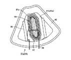
図4は、プラズマ発生器の一例を示す縦断面図である。また、図5は、プラズマ発生器の一例を示す分解斜視図である。さらに、図6は、プラズマ発生器に設けられる筐体の一例を示す斜視図である。 FIG. 4 is a longitudinal sectional view showing an example of a plasma generator. FIG. 5 is an exploded perspective view showing an example of a plasma generator. Further, FIG. 6 is a perspective view showing an example of a housing provided in the plasma generator.
プラズマ発生器81a、81bは、金属線等から形成されるアンテナ83をコイル状に例えば鉛直軸回りに3重に巻回して構成されている。また、プラズマ発生器81は、平面視で回転テーブル2の径方向に伸びる帯状体領域を囲むように、且つ回転テーブル2上のウエハWの直径部分を跨ぐように配置されている。 The
アンテナ83は、整合器84を介して周波数が例えば13.56MHz及び出力電力が例えば5000Wの高周波電源85に接続されている。そして、このアンテナ83は、真空容器1の内部領域から気密に区画されるように設けられている。なお、図4において、アンテナ83と整合器84及び高周波電源85とを電気的に接続するための接続電極86が設けられている。 The
図4及び図5に示すように、第1のプラズマ処理用ガスノズル32の上方側における天板11には、平面視で概略扇形に開口する開口部11aが形成されている。 As shown in FIGS. 4 and 5, the
開口部11aには、図4に示すように、開口部11aの開口縁部に沿って、この開口部11aに気密に設けられる環状部材82を有する。後述する筐体90は、この環状部材82の内周面側に気密に設けられる。即ち、環状部材82は、外周側が天板11の開口部11aに臨む内周面11bに対向すると共に、内周側が後述する筐体90のフランジ部90aに対向する位置に、気密に設けられる。そして、この環状部材82を介して、開口部11aには、アンテナ83を天板11よりも下方側に位置させるために、例えば石英等の誘導体により構成された筐体90が設けられる。 As shown in FIG. 4, the opening 11 a has an
また、環状部材82は、図4に示すように、鉛直方向に伸縮可能なベローズ82aを有している。また、プラズマ発生器81a、81bは、電動アクチュエータ等の図示しない駆動機構(昇降機構)により、各々独立して昇降可能に形成されている。プラズマ発生器81a、81bの昇降に対応して、ベローズ82aを伸縮させることで、プラズマ処理時における、プラズマ発生器81a、81bの各々とウエハW(即ち、回転テーブル2)との間の距離、即ち、(以後、プラズマ生成空間の距離と呼ぶことがある)を変更可能に構成されている。 Further, as shown in FIG. 4, the
筐体90は、図6に示すように、上方側の周縁部が周方向に亘ってフランジ状に水平に伸び出してフランジ部90aをなすと共に、平面視において、中央部が下方側の真空容器1の内部領域に向かって窪むように形成されている。 As shown in FIG. 6, the
筐体90は、この筐体90の下方にウエハWが位置した場合に、回転テーブル2の径方向におけるウエハWの直径部分を跨ぐように配置されている。なお、環状部材82と天板11との間には、O−リング等のシール部材11cが設けられる。 The
真空容器1の内部雰囲気は、環状部材82及び筐体90を介して気密に設定されている。具体的には、環状部材82及び筐体90を開口部11a内に落とし込み、次いで環状部材82及び筐体90の上面であって、環状部材82及び筐体90の接触部に沿うように枠状に形成された押圧部材91によって筐体90を下方側に向かって周方向に亘って押圧する。さらに、この押圧部材91を図示しないボルト等により天板11に固定する。これにより、真空容器1の内部雰囲気は気密に設定される。なお、図5においては、簡単のため、環状部材82を省略して示している。 The internal atmosphere of the
図6に示すように、筐体90の下面には、当該筐体90の下方側の処理領域P2、P3の各々を周方向に沿って囲むように、回転テーブル2に向かって垂直に伸び出す突起部92が形成されている。そして、この突起部92の内周面、筐体90の下面及び回転テーブル2の上面により囲まれた領域には、前述した第1のプラズマ処理用ガスノズル32及び第2のプラズマ処理用ガスノズル33が収納されている。なお、第1のプラズマ処理用ガスノズル32及び第2のプラズマ処理用ガスノズル33の基端部(真空容器1の内壁側)における突起部92は、第2のプラズマ処理用ガスノズル33の外形に沿うように概略円弧状に切り欠かれている。 As shown in FIG. 6, the lower surface of the
筐体90の下方側には、図4に示すように、突起部92が周方向に亘って形成されている。シール部材11cは、この突起部92によって、プラズマに直接曝されず、即ち、プラズマ生成領域から隔離されている。そのため、プラズマ生成領域からプラズマが例えばシール部材11c側に拡散しようとしても、突起部92の下方を経由して行くことになるので、シール部材11cに到達する前にプラズマが失活することとなる。 As shown in FIG. 4, a
筐体90の上方側には、当該筐体90の内部形状に概略沿うように形成された導電性の板状体である金属板例えば銅などからなる、接地されたファラデーシールド95が収納されている。このファラデーシールド95は、筐体90の底面に沿うように水平に形成された水平面95aと、この水平面95aの外終端から周方向に亘って上方側に伸びる垂直面95bと、を備えており、平面視で例えば概略六角形となるように構成されていても良い。 A grounded
図7は、プラズマ発生器の一例を示す平面図である。図8は、プラズマ発生器に設けられるファラデーシールドの一部を示す斜視図である。 FIG. 7 is a plan view showing an example of a plasma generator. FIG. 8 is a perspective view showing a part of a Faraday shield provided in the plasma generator.
回転テーブル2の回転中心からファラデーシールド95を見た場合の右側及び左側におけるファラデーシールド95の上端縁は、各々、右側及び左側に水平に伸び出して支持部96を為している。そして、ファラデーシールド95と筐体90との間には、支持部96を下方側から支持すると共に筐体90の中心部領域C側及び回転テーブル2の外縁部側のフランジ部90aに各々支持される枠状体99が設けられている。 When the
アンテナ83によって生成した電界がウエハWに到達する場合、ウエハWの内部に形成されているパターン(電気配線等)が電気的にダメージを受けてしまう場合がある。そのため、図8に示すように、水平面95aには、アンテナ83において発生する電界及び磁界(電磁界)のうち電界成分が下方のウエハWに向かうことを阻止すると共に、磁界をウエハWに到達させるために、多数のスリット97が形成されている。 When the electric field generated by the
スリット97は、図7及び図8に示すように、アンテナ83の巻回方向に対して直交する方向に伸びるように、周方向に亘ってアンテナ83の下方位置に形成されている。ここで、スリット97は、アンテナ83に供給される高周波に対応する波長の1/10000以下程度の幅寸法となるように形成されている。また、各々のスリット97の長さ方向における一端側及び他端側には、これらスリット97の開口端を塞ぐように、接地された導電体等から形成される導電路97aが周方向に亘って配置されている。ファラデーシールド95においてこれらスリット97の形成領域から外れた領域、即ち、アンテナ83の巻回された領域の中央側には、当該領域を介してプラズマの発光状態を確認するための開口部98が形成されている。なお、前述した図2においては、簡単のために、スリット97を省略しており、スリット97の形成領域例を、一点鎖線で示している。 As shown in FIGS. 7 and 8, the
図5に示すように、ファラデーシールド95の水平面95a上には、ファラデーシールド95の上方に載置されるプラズマ発生器81a、81bとの間の絶縁性を確保するために、厚み寸法が例えば2mm程度の石英等から形成される絶縁板94が積層されている。即ち、プラズマ発生器81a、81bは、各々、筐体90、ファラデーシールド95及び絶縁板94を介して真空容器1の内部(回転テーブル2上のウエハW)に対向するように配置されている。 As shown in FIG. 5, on the
このように、第1のプラズマ発生器81aと第2のプラズマ発生器81bとは、ほぼ同様な構成を有するが、設置される高さが異なっている。即ち、回転テーブル2の表面と第1のプラズマ発生器81aとの間の距離と、回転テーブル2の表面と第2のプラズマ発生器81bとの間の距離とが異なっている。これは、筐体90の底面の高さを調整することにより、容易に高さを異ならせることができる。 Thus, although the
具体的には、第1のプラズマ発生器81aの高さの方が、第2のプラズマ発生器81bの高さよりも高く設定される。上述のように、第1のプラズマ発生器81aの下方の領域は、筐体90により実質的に閉じられた第2の処理領域P2が形成されており、第2のプラズマ発生器81bの下方の領域も、筐体90により実質的に閉じられた第3の処理領域P3が形成されている。よって、回転テーブル2の表面との距離が小さい方、即ち、プラズマ発生器81a、81bが低く設置されている方が、より狭い空間を形成する。ここで、第2の処理領域P2における第1のプラズマ発生器81aと回転テーブル2の表面との間の距離を第1の距離、第3の処理領域P3における第2のプラズマ発生器81bと回転テーブル2の表面との間の距離を第2の距離とすると、第1の距離よりも相対的に小さい第2の距離によって、第3の処理領域P3においては、ウエハWに到達するイオン量が、第2の処理領域P2と比較して多くなる。よって、第3の処理領域P3においては、ウエハWに到達するラジカル量も、第2の処理領域P2と比較して多くなる。 Specifically, the height of the
なお、第1のプラズマ発生器81aと回転テーブル2の表面との間の第1の距離と、第2のプラズマ発生器81bと回転テーブル2の表面との間の第2の距離は、第1の距離が第2の距離より大きい限り、種々の値とすることができるが、例えば、第1の距離が80mm以上150mm以下、第2の距離が20mm以上80mm未満の範囲内に設定されてもよい。ただし、距離は、用途に応じて種々変更することができ、これらの値に限定されるものではない。 The first distance between the
再び、本実施形態に係る成膜装置の他の構成要素について、説明する。 Again, other components of the film forming apparatus according to this embodiment will be described.
回転テーブル2の外周側において、回転テーブル2よりも僅かに下位置には、図2に示すように、カバー体であるサイドリング100が配置されている。サイドリング100の上面には、互いに周方向に離間するように例えば2箇所に排気口61、62が形成されている。別の言い方をすると、真空容器1の床面には、2つの排気口が形成され、これら排気口に対応する位置におけるサイドリング100には、排気口61、62が形成されている。 On the outer peripheral side of the
本明細書においては、排気口61、62のうち一方及び他方を、各々、第1の排気口61、第2の排気口62と呼ぶ。ここでは、第1の排気口61は、分離ガスノズル42と、この分離ガスノズル42に対して、回転テーブルの回転方向下流側に位置する第1のプラズマ発生器81aとの間に形成されている。また、第2の排気口62は、第2のプラズマ発生器81bと、このプラズマ発生器81bよりも回転テーブル2の回転方向下流側の分離領域Dとの間に形成されている。 In the present specification, one and the other of the
第1の排気口61は、第1の処理ガスや分離ガスを排気するためのものであり、第2の排気口62は、プラズマ処理用ガスや分離ガスを排気するためのものである。これら第1の排気口61及び第2の排気口62は、各々、バタフライバルブ等の圧力調整部65が介設された排気管63により、真空排気機構である例えば真空ポンプ64に接続されている。 The first exhaust port 61 is for exhausting the first processing gas and the separation gas, and the
前述したように、中心部領域C側から外縁側に亘って筐体90を配置しているため、プラズマ処理領域P2、P3に対して回転テーブル2の回転方向上流側から通流してくるガスは、この筐体90によって排気口62に向かおうとするガス流が規制されてしまうことがある。そのため、筐体90よりも外周側におけるサイドリング100の上面には、ガスが流れるための溝状のガス流路101(図1及び図2参照)が形成されている。 As described above, since the
天板11の下面における中央部には、図1に示すように、凸状部4における中心部領域C側の部位と連続して周方向に亘って概略リング状に形成されると共に、その下面が凸状部4の下面(天井面44)と同じ高さに形成された突出部5が設けられている。この突出部5よりも回転テーブル2の回転中心側におけるコア部21の上方側には、中心部領域Cにおいて各種ガスが互いに混ざり合うことを抑制するためのラビリンス構造部110が配置されている。 As shown in FIG. 1, the bottom surface of the
前述したように筐体90は中心部領域C側に寄った位置まで形成されているので、回転テーブル2の中央部を支持するコア部21は、回転テーブル2の上方側の部位が筐体90を避けるように回転中心側に形成されている。そのため、中心部領域C側では、外縁部側よりも、各種ガス同士が混ざりやすい状態となっている。そのため、コア部21の上方側にラビリンス構造部110を形成することにより、ガスの流路を稼ぎ、ガス同士が混ざり合うことを防止することができる。 As described above, since the
より具体的には、ラビリンス構造部110は、回転テーブル2側から天板11側に向かって垂直に伸びる壁部と、天板11側から回転テーブル2に向かって垂直に伸びる壁部とが、各々周方向に亘って形成されると共に、回転テーブル2の半径方向において交互に配置された構造を有する。ラビリンス構造部110では、例えば原料ガスノズル31から吐出されて中心部領域Cに向かおうとする第1の処理ガスは、ラビリンス構造部110を乗り越えていく必要がある。そのため、中心部領域Cに向かうにつれて流速が遅くなり、拡散しにくくなる。結果として、処理ガスが中心部領域Cに到達する前に、中心部領域Cに供給される分離ガスにより、処理領域P1側に押し戻されることになる。また、中心部領域Cに向かおうとする他のガスについても、同様にラビリンス構造部110によって中心部領域Cに到達しにくくなる。そのため、処理ガス同士が中心部領域Cにおいて互いに混ざり合うことが防止される。 More specifically, the
回転テーブル2と真空容器1の底面部14との間の空間には、図1に示すように、加熱機構であるヒータユニット7が設けられている。ヒータユニット7は、回転テーブル2を介して回転テーブル2上のウエハWを例えば室温〜760℃程度に加熱することができる構成となっている。なお、図1における参照符号71aは、ヒータユニット7の側方側に設けられたカバー部材であり、参照符号7aは、このヒータユニット7の上方側を覆う覆い部材である。また、真空容器1の底面部14には、ヒータユニット7の下方側において、ヒータユニット7の配置空間をパージするためのパージガス供給管73が、周方向に亘って複数個所に設けられている。 As shown in FIG. 1, a heater unit 7 serving as a heating mechanism is provided in a space between the rotary table 2 and the bottom surface portion 14 of the
図2に示すように、真空容器1の側壁には、ウエハWの受け渡しを行うための搬送口15が形成されている。この搬送口15は、ゲートバルブGより気密に開閉自在に構成されている。 As shown in FIG. 2, a
回転テーブル2の凹部24は、この搬送口15に臨む位置にて搬送アーム10との間でウエハWの受け渡しが行われる。そのため、回転テーブル2の下方側の受け渡し位置に対応する箇所には、凹部24を貫通してウエハWを裏面から持ち上げるための図示しない昇降ピン及び昇降機構が設けられている。 The
また、本実施形態に係る成膜装置には、装置全体の動作を制御するためのコンピュータからなる制御部120が設けられている。この制御部120のメモリ内には、後述の基板処理を行うためのプログラムが格納されている。このプログラムは、装置の各種動作を実行するようにステップ群が組まれており、ハードディスク、コンパクトディスク、光磁気ディスク、メモリカード、フレキシブルディスク等の記憶媒体である記憶部121から制御部120内にインストールされる。 In addition, the film forming apparatus according to the present embodiment is provided with a
〔成膜方法〕
次に、本発明の実施形態に係る成膜方法について説明する。本発明の実施形態に係る成膜方法は、ALD法(Atomic Layer Deposition、原子層堆積法)又はMLD法(Molecular Layer Deposition、分子層堆積法)による成膜が可能な成膜装置であれば、種々の成膜装置により実施することができるが、本実施形態では、上述の回転テーブル式の成膜装置を用いて実施する例について説明する。[Film formation method]
Next, a film forming method according to an embodiment of the present invention will be described. The film forming method according to the embodiment of the present invention is a film forming apparatus capable of forming a film by the ALD method (Atomic Layer Deposition) or the MLD method (Molecular Layer Deposition). Although various film forming apparatuses can be used, in this embodiment, an example in which the above-described rotary table type film forming apparatus is used will be described.
なお、第1のプラズマ処理を行う第2の処理領域P2におけるプラズマ発生器81aと回転テーブル2との間の第1の距離が、第2のプラズマ処理を行う第3の処理領域P3におけるプラズマ発生器81bと回転テーブル2との間の第2の距離よりも大きく設定した例を挙げて説明する。また、原料ガスノズル31から供給する原料ガスとしてはDCS(SiH2Cl2、ジクロロシラン)、第1のプラズマ処理用ガスノズル32から供給する第1のプラズマ処理用ガスとしてはNH3、Ar及びH2の混合ガス、第2のプラズマ処理用ガスノズル33から供給する第2のプラズマ処理用ガスノズルとしてはNH3、N2及び、Arの混合ガスを用いる例を挙げて説明する。但し、これらは一例として挙げるものであり、原料ガスとしては種々のSi含有ガス、第1のプラズマ処理用ガスとしては種々の窒化ガス、第2のプラズマ処理用ガスとしては種々のNH3及びN2の双方を含有する改質ガスを用いることができる。It should be noted that the first distance between the
本実施形態では、第1のプラズマ処理用ガスとして、NH3を含有するがN2を含有しない窒化ガスを用い、第2のプラズマ処理用ガスとして、NH3及びN2を含有する改質ガスを用いるが、まず、その理由について説明する。In the present embodiment, a nitriding gas containing NH3 but not containing N2 is used as the first plasma processing gas, and a reformed gas containing NH3 and N2 is used as the second plasma processing gas. First, the reason will be described.
プラズマ中で、NH3、N2が単独のガスとして各々存在する場合には、以下の式(1)、(2)に示すように、各々で可逆反応が発生する。When NH3 and N2 each exist as a single gas in the plasma, a reversible reaction occurs in each as shown in the following formulas (1) and (2).
NH3⇔NH2*+H* (1)
N2⇔2N* (2)
2つのガスがプラズマ中に存在する場合には、以下の式(3)〜(5)に示すように、N*がH*と反応することで、NH*、NH2*の双方が発生し、窒化力が増加するとともに、式(1)、(2)の可逆反応を防ぐ。NH3 ⇔NH2* + H* (1)
N2 ⇔ 2N* (2)
If the two gases are present in the plasma, as shown in the following equation (3) to (5),by N * reacts withH *, NH *, NH 2 * both occurred As the nitriding power increases, the reversible reaction of formulas (1) and (2) is prevented.
N*+H*→NH* (3)
NH*+H*→NH2* (4)
NH2*+H*→NH3 (5)
よって、式(6)に示されるように、結果的には、NH3にN2を添加してプラズマにより活性化することにより、窒化力を増加させる方向に作用する。N* + H* → NH* (3)
NH* + H* → NH2* (4)
NH2* + H* → NH3 (5)
Therefore, as shown in Expression (6), as a result, N2 is added to NH3 and activated by plasma, thereby acting in the direction of increasing nitriding power.
2NH3+N2⇔2NH2*+2NH* (6)
かかるメカ二ズムを利用し、本実施形態では、改質用の第2のプラズマ処理用ガスとして、NH3とN2との混合ガスを用い、窒化力を高め、膜質を向上させる。2NH3 + N2 ⇔2NH2* + 2NH* (6)
Using this mechanism, in this embodiment, a mixed gas of NH3 and N2 is used as the second plasma processing gas for reforming to increase the nitriding power and improve the film quality.
但し、N2がある濃度以上になった場合には、窒化ガスであるNH3を希釈し過ぎ、窒化源であるNH3が不足してしまうので、NH3/N2の最適な流量比が存在する。以下、その流量比についても言及しつつ本発明の実施形態に係る成膜方法について説明する。However, if it becomes more than a certain concentration is N2 is too dilute NH3 is a gas nitriding, since NH3 is nitrided source is insufficient, optimum flow ratio of NH 3/ N2 is Exists. Hereinafter, a film forming method according to an embodiment of the present invention will be described with reference to the flow rate ratio.
先ず、上述した成膜装置へのウエハWの搬入に際しては、先ず、ゲートバルブGを開放する。そして、回転テーブル2を間欠的に回転させながら、搬送アーム10により搬送口15を介して回転テーブル2上に載置する。 First, when loading the wafer W into the film forming apparatus described above, the gate valve G is first opened. Then, the rotary table 2 is placed on the rotary table 2 via the
次いで、ゲートバルブGを閉じて、ヒータユニット7により、ウエハWを所定の温度に加熱する。ウエハWの温度は、用途に応じて適宜適切な値に設定されてよいが、300〜600℃の範囲に設定されてもよく、例えば、400℃程度に設定されてもよい。 Next, the gate valve G is closed, and the wafer W is heated to a predetermined temperature by the heater unit 7. The temperature of the wafer W may be set to an appropriate value depending on the use, but may be set in a range of 300 to 600 ° C., for example, may be set to about 400 ° C.
続いて、第1の処理ガスノズル31から原料ガスであるDCSを、所定の流量で供給すると共に、第1のプラズマ処理用ガスノズル32及び第2のプラズマ処理用ガスノズル34から、所定の流量で第1及び第2のプラズマ処理用ガスを供給する。ここで、第1のプラズマ処理用ガスはNH3、Ar及びH2の混合ガスであり、第2のプラズマ処理用ガスはNH3、N2及び、Arの混合ガスである。第1のプラズマ処理用ガスは、ウエハWの表面に吸着したSi含有ガスと反応してSiN膜の分子層をウエハWの表面上に堆積させるための窒化ガスであり、第2のプラズマ処理用ガスは、ウエハWの表面上に堆積したSiN膜を更に窒化し、SiN膜の膜質を向上させるための改質ガスである。改質ガスが、上述の式(6)の反応を発生するガスであり、窒化力を高める効果を有する。Subsequently, DCS, which is a raw material gas, is supplied from the first
そして、圧力調整部65により真空容器1内を所定の圧力に調整する。また、プラズマ発生器81a、81bでは、各々、アンテナ83に対して、所定の出力の高周波電力を印加する。なお、圧力は、用途に応じて適切な値に設定されてよいが、0.2〜2.0Torrの範囲に設定されてもよく、例えば、0.75Torr程度に設定されてもよい。 Then, the inside of the
以下、図2を用いて説明する。ウエハWの表面では、回転テーブル2の回転によって第1の処理領域P1において原料ガス(Si含有ガス)であるDCSが吸着する。第1の処理ガスが吸着したウエハWは、回転テーブル2の回転により、分離領域Dを通過する。この分離領域Dでは、ウエハWの表面に分離ガスが供給され、第1の処理ガスに関する、不要な物理吸着分が除去される。 Hereinafter, a description will be given with reference to FIG. On the surface of the wafer W, DCS that is a source gas (Si-containing gas) is adsorbed by the rotation of the
ウエハWは次に、回転テーブル2の回転により、第2の処理領域P2に到達する。第2の処理領域P2では、第1のプラズマ処理用ガスノズル32から供給された第1のプラズマ処理用ガス(NH3含有ガス)がプラズマによって活性化され、NH2*によりDCSが窒化され、形成したシリコン窒化膜(SiN膜)がウエハWの表面上に堆積する。Next, the wafer W reaches the second processing region P <b> 2 by the rotation of the
ここで、第1のプラズマ処理用ガスは、NH3含有ガス等の窒化ガスであれば、種々のガスを用いることができるが、例えば、Ar、NH3及びH2を含む混合ガスであってもよい。また、Ar、NH3及びH2の含有量及び比率も、用途に応じて種々の設定としてよいが、例えば、Arを2000sccm、NH3を300sccm、H2を600sccm含む混合ガスであってもよい。第1のプラズマ処理用ガスは、ウエハWの表面に吸着したSi成分の窒化に重点を置き、窒化源であるNH3を十分に供給する。よって、第1のプラズマ処理用ガスには、N2を含まない。また、第1のプラズマ発生器81aは、第2のプラズマ発生器81bよりも高い位置に設置され、NH3をプラズマ化したNH2*がウエハWの全面に広く行き渡るようにする。NH2*は、広く拡散する性質を有するので、この役割に適していると言える。Here, various gases can be used as the first plasma processing gas as long as it is a nitriding gas such as an NH3 -containing gas. For example, the first plasma processing gas is a mixed gas containing Ar, NH3 and H2. Also good. Further, the contents and ratios of Ar, NH3 and H2 may be variously set according to the use, but for example, a mixed gas containing 2000 sccm of Ar, 300 sccm of NH3 and 600 sccm of H2 may be used. . The first plasma processing gas focuses on nitriding the Si component adsorbed on the surface of the wafer W, and sufficiently supplies NH3 as a nitriding source. Therefore, the first plasma processing gas does not contain N2 . The
なお、一般的に、プラズマ処理用のガスのプラズマによって発生する活性種としては、イオン及びラジカルが知られており、イオンは、主として窒化膜の改質処理に寄与し、ラジカルは、主として窒化膜の形成処理に寄与する。また、イオンは、ラジカルと比較して、寿命が短く、プラズマ発生部81a、81bと、回転テーブル2との間の距離を長くすることにより、ウエハWに到達するイオンエネルギーが大きく減少する。 In general, ions and radicals are known as active species generated by plasma of gas for plasma processing. The ions mainly contribute to the reforming treatment of the nitride film, and the radicals are mainly nitride film. It contributes to the formation process. In addition, ions have a shorter lifetime than radicals, and by increasing the distance between the
ここで、第2の処理領域P2では、第1のプラズマ発生部81aと回転テーブル2との間の距離が、第2の距離と比較して大きい距離に設定されている。この比較的大きい第1の距離によって、第2の処理領域P2において、ウエハWに到達するイオンは大きく低減され、ウエハWには主としてラジカルが供給される。即ち、第2の処理領域P2においては、ウエハW上の第1の処理ガスは、比較的イオンエネルギーが小さいプラズマによって、(初期)窒化され、薄膜成分である窒化膜の分子層が1層又は複数層形成される。また、形成された窒化膜は、プラズマによって、ある程度の改質処理もなされる。 Here, in the second processing region P2, the distance between the first
また、成膜プロセスの初期においては、活性種のウエハへの影響が大きく、例えばイオンエネルギーが大きいプラズマを使用した場合、ウエハ自身が窒化されてしまうことがある。この観点からも、第2の処理領域P2における処理では、先ず、比較的イオンエネルギーが小さいプラズマによってプラズマ処理を行うことが好ましい。 Further, in the initial stage of the film forming process, the active species has a great influence on the wafer. For example, when plasma with high ion energy is used, the wafer itself may be nitrided. Also from this viewpoint, in the processing in the second processing region P2, first, it is preferable to perform plasma processing with plasma having relatively low ion energy.
第1の距離としては、限定されないが、比較的イオンエネルギーが小さいプラズマによって、効率的にウエハW上に窒化膜を成膜する観点から、80mm以上150mm以下の範囲内とすることが好ましく、例えば、90mmに設定してもよい。 The first distance is not limited, but is preferably within the range of 80 mm or more and 150 mm or less from the viewpoint of efficiently forming a nitride film on the wafer W with plasma having relatively low ion energy. , 90 mm may be set.
次に、第2の処理領域P2を通過したウエハWは、回転テーブル2の回転により、第3の処理領域P3に到達する。第3の処理領域P3では、第2のプラズマ処理用ガスノズル33から供された第2のプラズマ処理用ガスをプラズマで活性化することにより、SiN膜が更に窒化され、堆積したSiN膜が改質処理される。 Next, the wafer W that has passed through the second processing region P2 reaches the third processing region P3 due to the rotation of the
ここで、第2のプラズマ処理用ガスは、NH3及びN2の双方を含有する改質ガスであれば、種々のガスを用いることができるが、例えば、Ar、NH3及びN2を含む混合ガスであってもよい。また、Ar、NH3及びN2の含有量(流量)及び比率も、用途に応じて種々の設定としてよいが、NH3対N2の比率は、N2がNH3よりも高い流量を有する比率に設定されることが好ましく、N2がNH3の2倍以上の流量を有する比率に設定されることがより好ましい。更に、N2がNH3の3倍以上の流量を有する比率に設定されることが更に好ましく、N2がNH3の3倍以上の流量を有する比率に設定されることがより一層好ましい。例えば、Arの流量を2000sccmとしたときに、NH3(sccm)/N2(sccm)は、600/1400、500/1500、300/1700、200/1800といった比率とすることができる。後に、実施例を用いて説明するが、上述の比率のうち、最も良好な面内均一性で成膜できたのは、NH3/N2=300/1700であった。このように、第2のプラズマ処理用ガスのNH3/N2の比率は、N2がNH3の3倍以上の含有量となるような設定であることが好ましい。Here, as long as the second plasma processing gas is a modified gas containing both NH3 and N2 , various gases can be used. For example, Ar, NH3 and N2 are included. A mixed gas may be used. Also, the content (flow rate) and ratio of Ar, NH3 and N2 may be variously set depending on the application, but the ratio of NH3 to N2 is such that N2 has a higher flow rate than NH3. The ratio is preferably set, and more preferably, N2 is set to a ratio having a flow rate twice or more that of NH3 . Further, more preferably the N2 is set to a ratio with a 3-fold or more of the flow rate of NH3, N2 is it is more preferable to set the ratio with more than three times the flow rate of NH3. For example, when the flow rate of Ar is 2000 sccm, NH3 (sccm) / N2 (sccm) can be a ratio of 600/1400, 500/1500, 300/1700, 200/1800. As will be described later with reference to examples, among the above ratios, NH3 / N2 = 300/1700 was formed with the best in-plane uniformity. Thus, the NH3 / N2 ratio of the second plasma processing gas is preferably set so that N2 has a content three times or more that of NH3 .
このような比率でNH3及びN2を含有する混合ガスを第2のプラズマ処理用ガスノズル33から供給し、第2のプラズマ発生器81bで発生したプラズマを用いて活性化することにより、上述の式(6)で説明した反応が起こり、窒化力を高めることができる。また、N2のプラズマは、寿命は短いが、高いエネルギーを有するとともに、あまり拡散せず、アンテナ83の下に集中する性質がある。第2のプラズマ発生器81bのアンテナ83は、半径方向においてウエハWの両端よりも長く形成されているので、アンテナ83の下にNH2*、NH*を集中させることができ、ウエハWの径方向端部にあるSiN膜も十分に窒化することができる。これにより、ウエハW上のSiN膜の面内均一性を高めることができる。A gas mixture containing NH3 and N2 at such a ratio is supplied from the second plasma processing
また、第3の処理領域P3では、第2のプラズマ発生部81bと回転テーブル2との間の距離が、前述した第1の距離よりも小さい第2の距離に設定されている。第1の距離よりも相対的に小さい第2の距離によって、第3の処理領域P3においては、ウエハWに到達するイオン量が、第2の処理領域P2と比較して多くなる。なお、留意すべきことは、第3の処理領域P3においては、ウエハWに到達するラジカル量も、第2の処理領域P2と比較して多くなるということである。したがって、第3の処理領域P3においては、ウエハW上の第1の処理ガスは、比較的イオンエネルギーが大きく、高密度のラジカルを有するプラズマによって、窒化され、形成された窒化膜は、第2の処理領域P2と比較して、より効率的に改質処理される。 In the third processing region P3, the distance between the
第2の距離としては、第1の距離よりも小さければ限定されないが、より効率的に窒化膜を改質する観点から、20mm以上80mm未満の範囲内とすることが好ましく、例えば、60mmの距離(高さ)に設定してもよい。 The second distance is not limited as long as it is smaller than the first distance, but is preferably within a range of 20 mm or more and less than 80 mm from the viewpoint of more efficiently modifying the nitride film, for example, a distance of 60 mm. (Height) may be set.
プラズマ処理されたウエハWは、回転テーブル2の回転により、分離領域Dを通過する。この分離領域Dは、不要な窒化ガス、改質ガスが、第1の処理領域P1へと侵入しないように、第1の処理領域P1と第3の処理領域P3とを分離する領域である。 The plasma-treated wafer W passes through the separation region D by the rotation of the
本実施形態においては、回転テーブル2の回転を続けることにより、ウエハW表面への原料ガス(Si含有ガス)の吸着、ウエハW表面に吸着した原料ガス成分(Si)の窒化、及び反応生成物(SiN)のプラズマ改質が、この順番で多数回に亘って行われる。即ち、ALD法による成膜処理と、形成された膜の改質処理とが、回転テーブル2の回転よって、多数回に亘って行われる。 In the present embodiment, by continuing the rotation of the
なお、本実施形態に係る基板処理装置における処理領域P1、P2の間には、回転テーブル2の周方向両側に分離領域Dを配置している。そのため、分離領域Dにおいて、原料ガスとプラズマ処理用ガスとの混合が阻止されながら、各ガスが排気口61、62に向かって排気されていく。 Note that separation regions D are arranged on both sides in the circumferential direction of the
〔実施例〕
次に、本発明の実施形態に係る成膜方法を実施した実施例について説明する。まず、実施例に用いた成膜装置は、上述の実施形態で説明した回転テーブル式の2つのプラズマ発生器81a、81bを搭載したALD成膜装置である。〔Example〕
Next, examples in which the film forming method according to the embodiment of the present invention is implemented will be described. First, the film forming apparatus used in the examples is an ALD film forming apparatus on which the two rotary table
真空容器1内のウエハWの温度は、400℃に設定した。真空容器1内の圧力は、0.75Torrとした。回転テーブル2の回転速度は10rpmに設定した。第2の処理領域P2、即ち第1のプラズマ処理用ガスを供給する第1のプラズマ発生器81aの回転テーブル2の表面との距離は90mmに設定した。また、第3の処理領域P3、即ち第2のプラズマ処理用ガスを供給する第2のプラズマ発生器81bの回転テーブル2の表面との距離は60mmに設定した。原料ガスノズル31から供給される原料ガスは、Si含有ガスであるDCSを用い、流量は1000sccmに設定した。第1のプラズマ処理用ガスノズル32から供給される窒化ガスは、NH3/Ar/H2の混合ガスとし、NH3の流量を300sccm、Arの流量を2000sccm、H2の流量を600sccmに設定した。以上は、固定された条件である。The temperature of the wafer W in the
第2のプラズマ処理用ガスノズル33から供給される改質ガスは、NH3/N2/Arの混合ガスとし、Arの流量は2000sccmで固定したが、NH3(sccm)/N2(sccm)の流量を種々変化させた。The reformed gas supplied from the second plasma processing
比較例がNH3(sccm)/N2(sccm)=2000/0であり、これは従来から実施されているN2を添加しない改質処理である。The comparative example is NH3 (sccm) / N2 (sccm) = 2000/0, which is a conventional reforming process without adding N2 .
実施例1がNH3(sccm)/N2(sccm)=1500/500であり、実施例2がNH3(sccm)/N2(sccm)=1000/1000である。実施例3がNH3(sccm)/N2(sccm)=500/1500であり、実施例4がNH3(sccm)/N2(sccm)=300/1700である。実施例5がNH3(sccm)/N2(sccm)=200/1800であり、参考例がNH3(sccm)/N2(sccm)=0/2000である。参考例は、N2を含有しているが、NH3を含有しておらず、NH3とN2の混合ガスではないので、実施例ではなく参考例としている。In Example 1, NH3 (sccm) / N2 (sccm) = 1500/500, and in Example 2, NH3 (sccm) / N2 (sccm) = 1000/1000. In Example 3, NH3 (sccm) / N2 (sccm) = 500/1500, and in Example 4, NH3 (sccm) / N2 (sccm) = 300/1700. Example 5 is NH3 (sccm) / N2 (sccm) = 200/1800, and the reference example is NH3 (sccm) / N2 (sccm) = 0/2000. Reference examples, while containing N2, contains no NH3, is not a mixed gas of NH3 and N2, is set to no Reference Examples in the Examples.
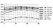
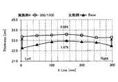
図9は、X軸上、即ち回転テーブル2の回転方向に略平行なウエハWの中心を通る横軸上における比較例、実施例1〜5及び参考例に係る成膜方法の実施結果を示した図である。図9において、横軸はウエハW上のX軸上における位置、縦軸はSiN膜の膜厚を示している。 FIG. 9 shows the results of implementation of the film forming methods according to the comparative examples, examples 1 to 5 and the reference example on the X axis, that is, on the horizontal axis passing through the center of the wafer W substantially parallel to the rotation direction of the
図9に示されるように、NH3(sccm)/N2(sccm)=300/1700の実施例4における膜厚が最も大きく、また、良好な均一性が得られている。N2が添加されていない比較例は、実施例1〜5のいずれよりも小さい膜厚となっている。また、NH3を含まない参考例は、比較例よりも更に膜厚が小さい。よって、図9より、X軸上において、実施例1〜6は総て比較例及び参考例よりも均一性が良好であり、そのうち実施例4のNH3(sccm)/N2(sccm)=300/1700の流量比が最も良好であることが示された。As shown in FIG. 9, the film thickness is the largest in Example 4 where NH3 (sccm) / N2 (sccm) = 300/1700, and good uniformity is obtained. The comparative example to which N2 is not added has a smaller film thickness than any of Examples 1 to 5. Moreover, the reference example which does not contain NH3 has a smaller film thickness than the comparative example. Therefore, from FIG. 9, on the X-axis, Examples 1 to 6 are all more uniform than the comparative example and the reference example, of which NH3 (sccm) / N2 (sccm) = A flow ratio of 300/1700 was shown to be the best.
図10は、Y軸上、即ち回転テーブル2の半径方向に平行なウエハWの中心を通る縦軸上における比較例、実施例1〜5及び参考例に係る成膜方法の実施結果を示した図である。図10において、横軸はウエハW上のY軸上における位置、縦軸はSiN膜の膜厚を示している。 FIG. 10 shows the execution results of the film forming methods according to the comparative examples, examples 1 to 5 and the reference example on the Y axis, that is, on the vertical axis passing through the center of the wafer W parallel to the radial direction of the
図10に示されるように、Y軸上においても、NH3(sccm)/N2(sccm)=300/1700の実施例4における膜厚が最も大きく、また、良好な均一性が得られている。N2が添加されていない比較例は、実施例1〜5のいずれよりも小さい膜厚となっている。また、NH3を含まない参考例は、比較例よりも更に膜厚が小さい点も、図9と同様である。よって、図10より、Y軸上においても、実施例1〜6は総て比較例及び参考例よりも均一性が良好であり、そのうち実施例4のNH3(sccm)/N2(sccm)=300/1700の流量比が最も良好であることが示された。As shown in FIG. 10, even on the Y axis, the film thickness in Example 4 where NH3 (sccm) / N2 (sccm) = 300/1700 was the largest, and good uniformity was obtained. Yes. The comparative example to which N2 is not added has a smaller film thickness than any of Examples 1 to 5. Moreover, the reference example which does not contain NH3 is the same as FIG. 9 in that the film thickness is smaller than that of the comparative example. Therefore, from FIG. 10, even on the Y-axis, Examples 1 to 6 are all more uniform than the comparative example and the reference example, of which NH3 (sccm) / N2 (sccm) of Example 4 = 300/1700 flow ratio was shown to be the best.
図11は、比較例、実施例1〜5及び参考例に係る成膜方法の成膜結果を面内均一性の観点から示した図である。図11において、横軸はN2濃度(%)を示し、右側に行く程N2密度が高くなる。また、縦軸は膜厚のウエハW内の均一性(±%)を示し、0に近付く程均一性は良好であることを意味する。FIG. 11 is a view showing the film formation results of the film forming methods according to the comparative example, Examples 1 to 5 and the reference example from the viewpoint of in-plane uniformity. In FIG. 11, the horizontal axis indicates the N2 concentration (%), and the N2 density increases toward the right side. The vertical axis indicates the uniformity (±%) of the film thickness within the wafer W, and the closer to 0, the better the uniformity.
図11に示されるように、実施例4のNH3(sccm)/N2(sccm)=300/1700の場合が最も均一性が良好であり、次に実施例5のNH3(sccm)/N2(sccm)=200/1800の場合の均一性が良好である。続いて、実施例3のNH3(sccm)/N2(sccm)=500/1500、新たに追加された実施例6のNH3(sccm)/N2(sccm)=600/1400、実施例2のNH3(sccm)/N2(sccm)=1000/1000、実施例1のNH3(sccm)/N2(sccm)=1500/500の順に良好となっている。そして、これら実施例1〜6の均一性は、いずれも比較例のNH3(sccm)/N2(sccm)=2000/0及び参考例のNH3(sccm)/N2(sccm)=0/2000の場合よりも高い。As shown in FIG. 11, NH3 (sccm) / N2 (sccm) in Example 4 has the best uniformity when 300/1700, and then NH3 (sccm) / in Example 5 The uniformity in the case of N2 (sccm) = 200/1800 is good. Subsequently,NH 3 of Example3 (sccm) / N 2 ( sccm) = 500/1500, NH 3 (sccm) / N 2 (sccm) = 600/1400 of Example 6 which is newly added, Example 2NH 3 (sccm) / N 2 (sccm) = 1000/1000, and has a good in the order ofNH 3 (sccm) / N 2 (sccm) = 1500/500 of example 1. The uniformity of these Examples 1-6,NH 3 in both Comparative Example(sccm) / N 2 (sccm ) = 2000/0 and Reference ExampleNH 3 in(sccm) / N 2 (sccm ) = 0 Higher than in the case of / 2000.
このように、実施例1〜6の膜厚の均一性は、総て比較例及び参考例よりも良好であり、その中でも、実施例4のNH3(sccm)/N2(sccm)=300/1700の比率が最も均一性が良好であることが示された。つまり、第2のプラズマ処理用ガスに用いる改質ガスには、NH3及びN2の双方を含有する混合ガスを用いることが好ましく、更に、N2の流量がNH3の流量よりも大きい所定の比率に面内均一性を良好にする最適値があることが示された。Thus, the film thickness uniformity of Examples 1 to 6 is all better than the comparative example and the reference example, and among them, NH3 (sccm) / N2 (sccm) = 300 of Example 4. A ratio of / 1700 was shown to be the most uniform. That is, the reformed gas used in the second plasma processing gas, it is preferable to use a mixed gas containing both NH3 and N2, further predetermined flow rate of N2 is greater than the flow rate of NH3 It has been shown that there is an optimum value for the in-plane uniformity in the ratio.
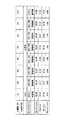
図12は、比較例、実施例1〜6及び参考例のウエハW上に成膜されたSiN膜の均一性の算出結果を示した図である。 FIG. 12 is a diagram showing the calculation result of the uniformity of the SiN film formed on the wafer W of the comparative example, Examples 1 to 6 and Reference Example.
図12において、膜厚の平均値がWIN AVG(nm)、最大値がMax(nm)、最小値がMin(nm)、均一性がWin Unif(±%)で示されている。図9〜図11で示した結果と合致して、均一性は実施例4が±1.16%で最も良好であり、次いで、実施例5が±1.32%で2番目に良好であり、実施例3が1.68で3番目に良好である。更に、±1.92%の実施例6、±2.48%の実施例2、±2.99の実施例1の順に均一性が良好であり、これらは、±3.72の比較例及び±5.35の参考例よりも良好な結果となっている。 In FIG. 12, the average value of the film thickness is indicated by WIN AVG (nm), the maximum value is Max (nm), the minimum value is Min (nm), and the uniformity is indicated by Win Unif (±%). Consistent with the results shown in FIGS. 9-11, the uniformity is best at ± 1.16% for Example 4 and then second best at ± 1.32% for Example 5. Example 3 is 1.68, the third best. Further, the uniformity is good in the order of ± 1.92% of Example 6, ± 2.48% of Example 2, and ± 2.99 of Example 1, and these are ± 3.72 comparative examples and The result is better than the reference example of ± 5.35.
また、膜厚に関しても、実施例4が23.09nmで最も厚くなっており、実施例1〜6の方が、比較例及び参考例よりも大きな膜厚が得られているが、均一性程には全体で大きな差は見られない。よって、本実施例によれば、所定の膜厚を得つつ、面内均一性を向上させることができる。 Also, regarding the film thickness, Example 4 is the thickest at 23.09 nm, and Examples 1 to 6 have a larger film thickness than Comparative Examples and Reference Examples. There is no significant difference in overall. Therefore, according to the present embodiment, in-plane uniformity can be improved while obtaining a predetermined film thickness.
図13は、実施例4と比較例のX軸上における膜厚分布を示した実施結果である。図13に示されるように、実施例4では、膜厚全体が向上しているとともに、左側と右側の端部の膜厚が比較例よりも大幅に向上し、全体として膜厚均一性が向上していることが分かる。即ち、比較例においては、X軸上の中央領域よりも左側と右側の端部の膜厚が大きく低下しており、山なりの膜厚分布となっているが、実施例4においては、左側と右側の端部の膜厚の低下が小さく、全体で略水平な膜厚分布が得られていることが分かる。 FIG. 13 shows the results of the film thickness distribution on the X-axis of Example 4 and the comparative example. As shown in FIG. 13, in Example 4, the overall film thickness is improved, and the film thickness at the left and right end portions is significantly improved as compared with the comparative example, and the film thickness uniformity is improved as a whole. You can see that That is, in the comparative example, the film thicknesses at the left and right end portions are greatly reduced from the central region on the X-axis, and the film thickness distribution is a mountain-like distribution. It can be seen that the decrease in film thickness at the right end is small and a substantially horizontal film thickness distribution is obtained as a whole.
このように、最適条件である実施例4に係る成膜方法によれば、比較例よりも膜厚均一性を大幅に向上させることができることが示された。 Thus, according to the film-forming method which concerns on Example 4 which is optimal conditions, it was shown that a film thickness uniformity can be improved significantly rather than a comparative example.
図14は、実施例4と比較例のY軸上における膜厚分布を示した実施結果である。図14に示されるように、実施例4では、X軸上と同様に、膜厚全体が向上しているとともに、軸側と外側の端部の膜厚が比較例よりも大幅に向上し、全体として膜厚均一性が向上していることが分かる。即ち、比較例においては、Y軸上の中央領域よりも軸側と外側の端部の膜厚が大きく低下しており、山なりの膜厚分布となっているが、実施例4においては、軸側と外側の端部の膜厚の低下が小さく、全体で略水平な膜厚分布が得られていることが分かる。特に、比較例では、外側において大きな膜厚の低下が見られるが、実施例4では、外側の膜厚が大幅に向上していることが分かる。 FIG. 14 shows the results of the film thickness distribution on the Y-axis of Example 4 and the comparative example. As shown in FIG. 14, in Example 4, as with the X-axis, the overall film thickness is improved, and the film thickness at the axial and outer end portions is greatly improved as compared to the comparative example. It can be seen that the film thickness uniformity is improved as a whole. That is, in the comparative example, the film thickness at the end on the axial side and the outer side of the central region on the Y axis is greatly reduced, and the film thickness distribution is a mountain, but in Example 4, It can be seen that the decrease in film thickness at the axial and outer end portions is small, and a substantially horizontal film thickness distribution is obtained as a whole. In particular, in the comparative example, a large decrease in film thickness is seen on the outside, but in Example 4, it can be seen that the film thickness on the outside is greatly improved.
このように、最適条件である実施例4に係る成膜方法によれば、比較例よりも膜厚均一性を大幅に向上させることができることが示された。 Thus, according to the film-forming method which concerns on Example 4 which is optimal conditions, it was shown that a film thickness uniformity can be improved significantly rather than a comparative example.
なお、実施例1〜6の条件は、飽くまで例示であり、更なる実験により、更に良好な条件を発見し得る。 In addition, the conditions of Examples 1-6 are illustrations until it gets tired, and further favorable conditions can be discovered by further experiment.
このように、本発明の実施形態及び実施例に係る成膜方法によれば、第1のプラズマ処理用ガスをNH3含有ガスとし、第2のプラズマ処理用ガスをNH3及びN2含有ガスとすることにより、窒化膜の面内均一性を向上させることができる。更に、第2のプラズマ処理用ガスにおいて、N2の含有比率をNH3よりも高くし、更に最適な条件を見出すことにより、面内均一性を大幅に向上させることができる。Thus, according to the film forming method according to the embodiment and the example of the present invention, the first plasma processing gas is an NH3 -containing gas, and the second plasma processing gas is an NH3 and N2 -containing gas. By doing so, the in-plane uniformity of the nitride film can be improved. Furthermore, in the second plasma processing gas, the in-plane uniformity can be greatly improved by making the content ratio of N2 higher than that of NH3 and finding optimum conditions.
以上、本発明の好ましい実施形態及び実施例について詳説したが、本発明は、上述した実施形態及び実施例に制限されることはなく、本発明の範囲を逸脱することなく、上述した実施形態及び実施例に種々の変形及び置換を加えることができる。 The preferred embodiments and examples of the present invention have been described in detail above. However, the present invention is not limited to the above-described embodiments and examples, and the above-described embodiments and examples can be performed without departing from the scope of the present invention. Various modifications and substitutions can be made to the embodiments.
1 真空容器
2 回転テーブル
24 凹部
31 原料ガスノズル
32 第1のプラズマ処理用ガスノズル
33 第2のプラズマ処理用ガスノズル
41、42 分離ガスノズル
81a、81b プラズマ発生器
83 アンテナ
90 筐体
P1、P2、P3 処理領域
T トレンチ
W ウエハDESCRIPTION OF
Claims (8)
Translated fromJapanese前記基板の表面にパージガスを供給する工程と、
前記基板の前記表面に窒化ガスを第1のプラズマにより活性化して供給し、前記基板の前記表面上に吸着した前記Si含有ガスを窒化し、SiN膜を堆積させる工程と、
前記基板の前記表面にNH3及びN2をN2がNH3の3倍以上の比率で含む改質ガスを第2のプラズマにより活性化して供給し、前記基板の前記表面上に堆積した前記SiN膜を改質する工程と、
前記基板の表面にパージガスを供給する工程と、を有し、
前記基板は、処理室内に設けられた回転テーブルの表面上に周方向に沿って載置され、
前記処理室内の前記回転テーブルの上方には、前記回転テーブルの回転方向に沿って順に配置されたSi含有ガス供給領域、第1のパージガス供給領域、窒化ガス供給領域、改質ガス供給領域及び第2のパージガス供給領域が設けられ、
前記回転テーブルを1回転させることにより、前記基板が前記Si含有ガス供給領域、前記第1のパージガス供給領域、前記窒化ガス供給領域、前記改質ガス供給領域及び前記第2のパージガス供給領域を通過することにより、前記Si含有ガスを吸着させる工程、前記パージガスを供給する工程、前記SiN膜を堆積させる工程、前記SiN膜を改質する工程及び前記パージガスを供給する工程を1サイクル行い、前記回転テーブルを連続的に複数回回転させることにより、前記1サイクルを複数回繰り返す成膜方法。Supplying a Si-containing gas to the surface of the substrate, and adsorbing the Si-containing gas to the surface of the substrate;
Supplying a purge gas to the surface of the substrate;
Activating and supplying a nitriding gas to the surface of the substrate by a first plasma, nitriding the Si-containing gas adsorbed on the surface of the substrate, and depositing a SiN film;
Wherein the NH3 and N2 on the surface of the substrateN2is a reformed gas activated by supplying a second plasma containing atleast three times the ratioofNH3, was deposited on the surface of the substrate A step of modifying theSiN film ;
Havea, a step of supplying a purge gas to the surface of thesubstrate,
The substrate is placed along the circumferential direction on the surface of a turntable provided in the processing chamber,
Above the turntable in the processing chamber, a Si-containing gas supply region, a first purge gas supply region, a nitriding gas supply region, a reformed gas supply region, and a first gas gas are disposed in order along the rotation direction of the turntable. 2 purge gas supply areas are provided,
By rotating the rotary table once, the substrate passes through the Si-containing gas supply region, the first purge gas supply region, the nitriding gas supply region, the reformed gas supply region, and the second purge gas supply region. The step of adsorbing the Si-containing gas, the step of supplying the purge gas, the step of depositing the SiN film, the step of modifying the SiN film, and the step of supplying the purge gas are performed in one cycle, and the rotation A film forming method inwhich the one cycle is repeated a plurality of times by continuously rotating the table a plurality of times .
前記改質ガス供給領域の上方の前記処理室の外部には第2のプラズマ発生器が設けられ、
前記第2のプラズマ発生器は、前記第1のプラズマ発生器よりも低い位置に設けられている請求項1乃至7のいずれか一項に記載の成膜方法。A first plasma generator is provided outside the processing chamber above the nitriding gas supply region,
A second plasma generator is provided outside the processing chamber above the reformed gas supply region,
The second plasma generator, film forming method according toany one of the first term of the claims are provided at a position lower than the plasma generator 1to 7.
Priority Applications (4)
| Application Number | Priority Date | Filing Date | Title |
|---|---|---|---|
| JP2016040217AJP6584347B2 (en) | 2016-03-02 | 2016-03-02 | Deposition method |
| US15/439,180US20170253964A1 (en) | 2016-03-02 | 2017-02-22 | Film deposition method |
| KR1020170024488AKR102103058B1 (en) | 2016-03-02 | 2017-02-24 | Film forming method |
| TW106106301ATWI675933B (en) | 2016-03-02 | 2017-02-24 | Film deposition method |
Applications Claiming Priority (1)
| Application Number | Priority Date | Filing Date | Title |
|---|---|---|---|
| JP2016040217AJP6584347B2 (en) | 2016-03-02 | 2016-03-02 | Deposition method |
Publications (2)
| Publication Number | Publication Date |
|---|---|
| JP2017157715A JP2017157715A (en) | 2017-09-07 |
| JP6584347B2true JP6584347B2 (en) | 2019-10-02 |
Family
ID=59723460
Family Applications (1)
| Application Number | Title | Priority Date | Filing Date |
|---|---|---|---|
| JP2016040217AActiveJP6584347B2 (en) | 2016-03-02 | 2016-03-02 | Deposition method |
Country Status (4)
| Country | Link |
|---|---|
| US (1) | US20170253964A1 (en) |
| JP (1) | JP6584347B2 (en) |
| KR (1) | KR102103058B1 (en) |
| TW (1) | TWI675933B (en) |
Families Citing this family (7)
| Publication number | Priority date | Publication date | Assignee | Title |
|---|---|---|---|---|
| US9564309B2 (en) | 2013-03-14 | 2017-02-07 | Asm Ip Holding B.V. | Si precursors for deposition of SiN at low temperatures |
| US9576792B2 (en) | 2014-09-17 | 2017-02-21 | Asm Ip Holding B.V. | Deposition of SiN |
| US10410857B2 (en) | 2015-08-24 | 2019-09-10 | Asm Ip Holding B.V. | Formation of SiN thin films |
| US20170218517A1 (en)* | 2016-02-01 | 2017-08-03 | Tokyo Electron Limited | Method of forming nitride film |
| US10580645B2 (en)* | 2018-04-30 | 2020-03-03 | Asm Ip Holding B.V. | Plasma enhanced atomic layer deposition (PEALD) of SiN using silicon-hydrohalide precursors |
| KR102675856B1 (en)* | 2020-01-20 | 2024-06-17 | 에이에스엠 아이피 홀딩 비.브이. | Method of forming thin film and method of modifying surface of thin film |
| KR20220081905A (en) | 2020-12-09 | 2022-06-16 | 에이에스엠 아이피 홀딩 비.브이. | Silicon precursors for silicon silicon nitride deposition |
Family Cites Families (24)
| Publication number | Priority date | Publication date | Assignee | Title |
|---|---|---|---|---|
| KR100469126B1 (en)* | 2002-06-05 | 2005-01-29 | 삼성전자주식회사 | Method of forming a thin film with a low hydrogen contents |
| US20060014384A1 (en)* | 2002-06-05 | 2006-01-19 | Jong-Cheol Lee | Method of forming a layer and forming a capacitor of a semiconductor device having the same layer |
| KR100841866B1 (en)* | 2005-02-17 | 2008-06-27 | 가부시키가이샤 히다치 고쿠사이 덴키 | Method for manufacturing semiconductor device and substrate processing apparatus |
| US8129290B2 (en)* | 2005-05-26 | 2012-03-06 | Applied Materials, Inc. | Method to increase tensile stress of silicon nitride films using a post PECVD deposition UV cure |
| US7713868B2 (en)* | 2007-03-30 | 2010-05-11 | Tokyo Electron Limited | Strained metal nitride films and method of forming |
| US8739214B2 (en)* | 2007-11-08 | 2014-05-27 | At&T Intellectual Property I, L.P. | Methods, computer program products, and virtual servers for a virtual collaborative environment |
| WO2013137115A1 (en)* | 2012-03-15 | 2013-09-19 | 東京エレクトロン株式会社 | Film forming process and film forming apparatus |
| TWI614813B (en)* | 2013-01-21 | 2018-02-11 | 半導體能源研究所股份有限公司 | Semiconductor device manufacturing method |
| US20140273530A1 (en)* | 2013-03-15 | 2014-09-18 | Victor Nguyen | Post-Deposition Treatment Methods For Silicon Nitride |
| TW202431651A (en)* | 2013-10-10 | 2024-08-01 | 日商半導體能源研究所股份有限公司 | Liquid crystal display device |
| KR101551199B1 (en)* | 2013-12-27 | 2015-09-10 | 주식회사 유진테크 | Cyclic deposition method of thin film and manufacturing method of semiconductor, semiconductor device |
| JP6262115B2 (en)* | 2014-02-10 | 2018-01-17 | 東京エレクトロン株式会社 | Substrate processing method and substrate processing apparatus |
| JP2015181149A (en)* | 2014-03-06 | 2015-10-15 | 株式会社日立国際電気 | Substrate processing apparatus, manufacturing method of semiconductor device, and recording medium |
| JP6084179B2 (en)* | 2014-04-09 | 2017-02-22 | 東京エレクトロン株式会社 | Substrate processing apparatus and substrate processing method |
| US9214333B1 (en)* | 2014-09-24 | 2015-12-15 | Lam Research Corporation | Methods and apparatuses for uniform reduction of the in-feature wet etch rate of a silicon nitride film formed by ALD |
| JP6548586B2 (en)* | 2016-02-03 | 2019-07-24 | 東京エレクトロン株式会社 | Deposition method |
| TWI722132B (en)* | 2016-03-13 | 2021-03-21 | 美商應用材料股份有限公司 | Selective deposition of silicon nitride films for spacer applications |
| JP6573575B2 (en)* | 2016-05-02 | 2019-09-11 | 東京エレクトロン株式会社 | Method of embedding recess |
| US10151029B2 (en)* | 2016-08-08 | 2018-12-11 | Tokyo Electron Limited | Silicon nitride film forming method and silicon nitride film forming apparatus |
| JP6778144B2 (en)* | 2017-04-25 | 2020-10-28 | 株式会社Kokusai Electric | Semiconductor device manufacturing methods, substrate processing devices and programs |
| JP7203515B2 (en)* | 2017-06-06 | 2023-01-13 | アプライド マテリアルズ インコーポレイテッド | Bottom-up growth of silicon oxide and silicon nitride using a sequential deposition-etch-processing method |
| JP6929209B2 (en)* | 2017-12-04 | 2021-09-01 | 東京エレクトロン株式会社 | Silicon nitride film deposition method and film deposition equipment |
| US10580645B2 (en)* | 2018-04-30 | 2020-03-03 | Asm Ip Holding B.V. | Plasma enhanced atomic layer deposition (PEALD) of SiN using silicon-hydrohalide precursors |
| US10985010B2 (en)* | 2018-08-29 | 2021-04-20 | Versum Materials Us, Llc | Methods for making silicon and nitrogen containing films |
- 2016
- 2016-03-02JPJP2016040217Apatent/JP6584347B2/enactiveActive
- 2017
- 2017-02-22USUS15/439,180patent/US20170253964A1/ennot_activeAbandoned
- 2017-02-24TWTW106106301Apatent/TWI675933B/enactive
- 2017-02-24KRKR1020170024488Apatent/KR102103058B1/enactiveActive
Also Published As
| Publication number | Publication date |
|---|---|
| JP2017157715A (en) | 2017-09-07 |
| KR20170102810A (en) | 2017-09-12 |
| KR102103058B1 (en) | 2020-04-21 |
| TW201800597A (en) | 2018-01-01 |
| US20170253964A1 (en) | 2017-09-07 |
| TWI675933B (en) | 2019-11-01 |
Similar Documents
| Publication | Publication Date | Title |
|---|---|---|
| JP6584347B2 (en) | Deposition method | |
| KR101885411B1 (en) | Substrate processing method and substrate processing apparatus | |
| JP6548586B2 (en) | Deposition method | |
| JP6661487B2 (en) | Method of forming silicon nitride film | |
| KR101922757B1 (en) | Plasma treatment method and plasma treatment apparatus | |
| JP6146160B2 (en) | Film forming method, storage medium, and film forming apparatus | |
| JP2011151343A (en) | Plasma processing apparatus | |
| JP7068937B2 (en) | Board processing equipment | |
| JP2019033228A (en) | Forming method of silicon nitride film and film forming apparatus | |
| JP6587514B2 (en) | Plasma processing method and plasma processing apparatus | |
| JP7002970B2 (en) | Film formation method and film formation equipment | |
| TWI672393B (en) | Film deposition method | |
| KR20180054448A (en) | Film forming apparatus | |
| JP2022163575A (en) | PLASMA GENERATOR, FILM-FORMING APPARATUS AND METHOD USING THE SAME |
Legal Events
| Date | Code | Title | Description |
|---|---|---|---|
| A621 | Written request for application examination | Free format text:JAPANESE INTERMEDIATE CODE: A621 Effective date:20180809 | |
| A977 | Report on retrieval | Free format text:JAPANESE INTERMEDIATE CODE: A971007 Effective date:20190520 | |
| A131 | Notification of reasons for refusal | Free format text:JAPANESE INTERMEDIATE CODE: A131 Effective date:20190528 | |
| A521 | Request for written amendment filed | Free format text:JAPANESE INTERMEDIATE CODE: A523 Effective date:20190724 | |
| TRDD | Decision of grant or rejection written | ||
| A01 | Written decision to grant a patent or to grant a registration (utility model) | Free format text:JAPANESE INTERMEDIATE CODE: A01 Effective date:20190806 | |
| A61 | First payment of annual fees (during grant procedure) | Free format text:JAPANESE INTERMEDIATE CODE: A61 Effective date:20190903 | |
| R150 | Certificate of patent or registration of utility model | Ref document number:6584347 Country of ref document:JP Free format text:JAPANESE INTERMEDIATE CODE: R150 | |
| R250 | Receipt of annual fees | Free format text:JAPANESE INTERMEDIATE CODE: R250 | |
| R250 | Receipt of annual fees | Free format text:JAPANESE INTERMEDIATE CODE: R250 | |
| R250 | Receipt of annual fees | Free format text:JAPANESE INTERMEDIATE CODE: R250 | |
| R250 | Receipt of annual fees | Free format text:JAPANESE INTERMEDIATE CODE: R250 |