JP6583913B2 - Fine channel device and measuring method - Google Patents
Fine channel device and measuring methodDownload PDFInfo
- Publication number
- JP6583913B2 JP6583913B2JP2015177331AJP2015177331AJP6583913B2JP 6583913 B2JP6583913 B2JP 6583913B2JP 2015177331 AJP2015177331 AJP 2015177331AJP 2015177331 AJP2015177331 AJP 2015177331AJP 6583913 B2JP6583913 B2JP 6583913B2
- Authority
- JP
- Japan
- Prior art keywords
- fitting member
- groove
- fine
- fluid
- microchannel
- Prior art date
- Legal status (The legal status is an assumption and is not a legal conclusion. Google has not performed a legal analysis and makes no representation as to the accuracy of the status listed.)
- Active
Links
Images


Landscapes
- Investigating, Analyzing Materials By Fluorescence Or Luminescence (AREA)
- Investigating Or Analysing Materials By Optical Means (AREA)
Description
Translated fromJapanese本発明は、流体を流す微細流路を備え、前記流体に含まれる物質を表面増強ラマン分光法により測定する際に用いられる微細流路デバイス及び測定方法に関する。 The present invention relates to a microchannel device and a measuring method that are provided with a microchannel through which a fluid flows, and that are used when a substance contained in the fluid is measured by surface-enhanced Raman spectroscopy.
従来、高速液体クロマトグラフ(HPLC)に代表されるクロマトグラフィーの分野では、流体に含まれる物質を同定することが重要であり、この物質を同定するための手法として、表面増強ラマン分光法(SERS:Surface Enhanced Raman Scattering)が注目されている(例えば、特許文献1参照)。 Conventionally, in the field of chromatography typified by high performance liquid chromatography (HPLC), it is important to identify a substance contained in a fluid, and surface enhanced Raman spectroscopy (SERS) is a method for identifying this substance. : Surface Enhanced Raman Scattering) (see, for example, Patent Document 1).
表面増強ラマン分光法では、流体を搬送する流路の内面に形成した表面増強ラマン分光測定用金属ナノ粒子(以下、金属ナノ粒子として適宜説明する)に励起光を照射して、この金属ナノ粒子から発光するラマン散乱光を測定する。そして、測定したラマン散乱光を解析することにより、物質を同定することができる。 In surface-enhanced Raman spectroscopy, metal nanoparticles for surface-enhanced Raman spectroscopy (hereinafter, appropriately described as metal nanoparticles) formed on the inner surface of a channel carrying fluid are irradiated with excitation light. The Raman scattered light emitted from is measured. And a substance can be identified by analyzing the measured Raman scattered light.
ここで、流体に含まれる物質を表面増強ラマン分光法により測定する場合、流体を搬送する流路の直径が大きいと、流体に含まれる物質が、流路の内面に形成した金属ナノ粒子と接触しにくくなるため、流路の直径を100μm程度に設定した微細流路を形成した微細流路デバイスを用いた手法が検討されている(例えば、特許文献1参照)。 Here, when a substance contained in a fluid is measured by surface-enhanced Raman spectroscopy, the substance contained in the fluid comes into contact with metal nanoparticles formed on the inner surface of the flow path when the diameter of the flow path for transporting the fluid is large. Therefore, a technique using a microchannel device in which a microchannel having a channel diameter of about 100 μm is formed has been studied (for example, see Patent Document 1).
しかしながら、従来技術には、次のような問題があった。従来技術に係る微細流路デバイスは、透明な基板の内部に微細溝を形成するとともに、この微細溝の溝内面に金属ナノ粒子を形成する加工処理を経て製造される。このような微細で特殊な加工処理を必要とする微細流路デバイスは、非常に高価なものとなっていた。このため、コストを抑制した微細流路デバイスが望まれていた。 However, the prior art has the following problems. The microchannel device according to the prior art is manufactured through a processing process in which fine grooves are formed inside a transparent substrate and metal nanoparticles are formed on the groove inner surface of the fine grooves. Such a fine channel device that requires fine and special processing has been very expensive. For this reason, there has been a demand for a fine channel device with reduced cost.
本発明は、このような状況に鑑みてなされたもので、コストを抑制した微細流路デバイス及び測定方法を提供することを目的とする。 This invention is made | formed in view of such a condition, and it aims at providing the microchannel device and measuring method which suppressed cost.
本発明の第1の特徴は、流体を流す微細流路を備え、前記流体に含まれる物質を表面増強ラマン分光法により測定する際に用いられる微細流路デバイスであって、所定方向に沿って延びる中空部が形成される管部材と、前記中空部に嵌合される嵌合部材と、を備え、前記嵌合部材を覆っている前記管部材の少なくともラマン分光測定部分は、透明な部材で形成され、前記嵌合部材の外周部には、前記管部材の内周部との間に前記微細流路を形成する微細溝が設けられており、前記微細溝の溝内面には、表面増強ラマン分光測定用金属ナノ粒子が形成されることを要旨とする。 A first feature of the present invention is a microchannel device that includes a microchannel for flowing a fluid, and is used when measuring a substance contained in the fluid by surface-enhanced Raman spectroscopy, along a predetermined direction. A tube member in which an extending hollow portion is formed; and a fitting member fitted into the hollow portion; at least a Raman spectroscopic measurement portion of the tube member covering the fitting member is a transparent member. A fine groove is formed on the outer peripheral portion of the fitting member to form the fine flow channel between the outer peripheral portion of the fitting member and the inner peripheral portion of the pipe member. The gist is that metal nanoparticles for Raman spectroscopy are formed.
本発明の第2の特徴は、上記特徴に係り、前記管部材は、中空チューブであることを要旨とする。 The second feature of the present invention relates to the above feature, and is summarized in that the tube member is a hollow tube.
本発明の第3の特徴は、上記特徴に係り、前記嵌合部材の外周部には、前記微細溝が螺旋状に形成されていることを要旨とする。 A third feature of the present invention is related to the above feature, and is summarized in that the fine groove is formed in a spiral shape on an outer peripheral portion of the fitting member.
本発明の第4の特徴は、上記特徴に係り、前記微細溝の断面形状は、V字形状、U字形状、コの字状の何れか、又は、それらの組合せであることを要旨とする。 A fourth feature of the present invention relates to the above feature, wherein the cross-sectional shape of the fine groove is any one of a V shape, a U shape, a U shape, or a combination thereof. .
本発明の第5の特徴は、上記特徴に係り、前記嵌合部材は、前記微細溝の溝底部に固定される微小部材を更に備え、前記金属ナノ粒子は、前記微小部材の外表面に形成されることを要旨とする。 A fifth feature of the present invention is the above feature, wherein the fitting member further includes a minute member fixed to a groove bottom of the minute groove, and the metal nanoparticles are formed on an outer surface of the minute member. The gist is that
本発明の第6の特徴は、流体を流す微細流路を備える微細流路デバイスを用いて、前記流体に含まれる物質を表面増強ラマン分光法により測定する工程を含み、前記微細流路デバイスは、所定方向に沿って延びる中空部が形成される管部材と、前記中空部に嵌合される嵌合部材と、を備え、前記嵌合部材を覆っている前記管部材の少なくともラマン分光測定部分は、透明な部材で形成され、前記嵌合部材の外周部には、前記管部材の内周部との間に前記微細流路を形成する微細溝が設けられており、前記微細溝の溝内面には、表面増強ラマン分光測定用金属ナノ粒子が形成されることを要旨とする。 A sixth feature of the present invention includes a step of measuring a substance contained in the fluid by surface-enhanced Raman spectroscopy using a microchannel device including a microchannel that allows fluid to flow, and the microchannel device includes: A tube member in which a hollow portion extending along a predetermined direction is formed, and a fitting member fitted into the hollow portion, and at least a Raman spectroscopic measurement portion of the tube member covering the fitting member Is formed of a transparent member, and the outer periphery of the fitting member is provided with a minute groove that forms the minute channel between the inner periphery of the tube member, and the groove of the minute groove The gist is that metal nanoparticles for surface enhanced Raman spectroscopy are formed on the inner surface.
本発明によれば、コストを抑制した微細流路デバイス及び測定方法を提供することができる。 ADVANTAGE OF THE INVENTION According to this invention, the microchannel device and measuring method which suppressed cost can be provided.
以下、本発明の第1実施形態について、図面を参照しながら説明する。 Hereinafter, a first embodiment of the present invention will be described with reference to the drawings.
[本発明の第1実施形態]
(測定システム1の構成)
図1は、本発明の第1実施形態に係る測定システム1の概略構成図である。本発明の第1実施形態に係る測定システム1は、フロー系において、流体に含まれる物質を表面増強ラマン分光法により同定する。[First embodiment of the present invention]
(Configuration of measurement system 1)
FIG. 1 is a schematic configuration diagram of a
図1に示すように、第1実施形態に係る測定システム1は、供給機10と、搬送管20,30と、微細流路デバイス100と、発光器40と、受光器50とを備える。 As shown in FIG. 1, the
供給機10は、フロー系の一部として、検体となる物質を含む流体を供給する。搬送管20,30は、中空状の管であり、流体を搬送する。微細流路デバイス100は、搬送管20,30の間において、搬送管20,30を連結するように配置されている。 The
発光器40は、微細流路デバイス100に励起光L1を照射し、受光器50は、励起光L1によって発光するラマン散乱光L2を受光する。受光器50によって受光されたラマン散乱光L2は、ラマンスペクトルとして解析される。なお、測定システム1は、分光器や解析装置などの他の機器(不図示)も備えているが、ここでは詳細な説明を省略する。 The
(微細流路デバイス100の構成)
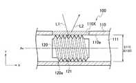
次に、微細流路デバイス100の構成について説明する。図2は、微細流路デバイス100の中心軸Axに沿った断面図である。なお、本実施形態では、図2に示すように、中心軸Axに沿ったX方向と、中心軸Axに直交するY方向とを規定する。図3は、図2における微細流路デバイス100の一部を拡大した拡大断面図である。(Configuration of microchannel device 100)
Next, the configuration of the
微細流路デバイス100は、流体を流す微細流路を備え、流体に含まれる物質を表面増強ラマン分光法により測定する際に用いられる。 The
図2に示すように、微細流路デバイス100は、所定方向に沿って延びる中空部111が形成される管部材110と、中空部111に嵌合される嵌合部材120と、を備える。すなわち、管部材110は、嵌合部材120を覆っている。なお、所定方向とは、流体の搬送方向であり、本実施形態では、微細流路デバイス100の中心軸Axに沿ったX方向である。 As shown in FIG. 2, the
本実施形態では、管部材110の少なくともラマン分光測定部分110Xは、透明な部材で形成される。ラマン分光測定部分110Xは、励起光L1及び散乱光L2が透過する部分である。ラマン分光測定部分110Xのサイズは、励起光L1を照射できるとともに、ラマン散乱光L2を受光できれば、特に制限はない。例えば、ラマン分光測定部分110Xのサイズは、中心軸Axに直交するY方向に沿って見た場合に、一辺2mm×2mm以上(4mm2以上)、もしくは、直径2mm以上としてもよい。なお、管部材110の全体が、透明な部材で形成されていてもよいことは無論である。In the present embodiment, at least the Raman
管部材110のラマン分光測定部分110Xの素材となる透明な部材は、一般に、表面増強ラマン分光法に使用される波長において透明な部材である。例えば、管部材110には、ガラス、プラスチックやシリコーンなどの樹脂、及び他の任意の部材を使用してもよい。なお、本実施形態において「透明」とは、波長が380nmから2000nmの波長帯域の特定波長の光に対して透過率が50%以上であることを意味している。管部材110のラマン分光測定部分110Xの光透過率は、80%以上であることが更に好ましい。また、管部材110のラマン分光測定部分110Xの光透過率は、その厚みを増減することで調節してもよい。 The transparent member that is the material of the Raman
本実施形態では、管部材110は、中空チューブである。例えば、管部材110は、シリコーンなどの弾性部材からなる円筒状の中空チューブである。 In the present embodiment, the
嵌合部材120は、管部材110の中空部111に嵌合される。嵌合部材120の外周部120aには、管部材110の内周部110aとの間に微細流路を形成する微細溝121が設けられている。 The
具体的に、微細溝121によって形成される外側端部123が管部材110の内周部110aに接することで、微細溝121と管部材110との間の隙間空間に微細流路が形成される。なお、微細溝121が微細流路を構成するとも言い換えることができる。微細溝121は、嵌合部材120のX方向の一方から他方に連続する。これにより、微細流路が、嵌合部材120のX方向の両側に連通する。 Specifically, the
本実施形態では、嵌合部材120の外周部120aには、微細溝121が螺旋状に形成されている。具体的に、微細溝121は、外周部120aにおいて、中心軸Axを中心とした螺旋状に延びている。 In the present embodiment, the
また、図3に示すように、微細溝121の延在方向に直交する方向において、微細溝121の断面形状は、V字形状である。微細溝121の溝幅Wgは、10μm〜1mmの範囲であることが好ましい。微細溝121の溝深さDgは、10μm〜100μmの範囲であることが好ましい。また、微細溝121の延在方向に直交する方向において、微細溝121の断面積は、100μm2〜0.1mm2の範囲であることが好ましい。As shown in FIG. 3, the cross-sectional shape of the
ここで、より安価に構成するという観点から、嵌合部材120には、規格に規定されるネジ(所謂、雄ネジ)を使用することが好ましい。なお、規格は、使用される地域に有効な産業規格によって定められており、例えば、JIS(日本工業規格)やISO(国際標準化機構)に規定される規格などである。 Here, it is preferable to use the screw (so-called male screw) prescribed | regulated to a specification for the
例えば、微細流路デバイス100では、内径D110が3mmの管部材110を使用した場合、嵌合部材120にM3のネジを使用してもよい。なお、管部材110の材料として弾性部材を用いた場合、管部材110は、中心軸Axに直交するY方向に伸張可能である。このため、嵌合部材120の直径D120は、管部材110の内径D110に対して、例えば5〜10%程度大きくてもよい。 For example, in the
嵌合部材120の素材には、鉄鋼材、特殊鋼材、ステンレス鋼材、アルミ、チタン、樹脂等の材料を適用できる。 Materials such as steel, special steel, stainless steel, aluminum, titanium, and resin can be applied to the material of the
嵌合部材120は、管部材110の中空部111に嵌合した状態で固定されている。本実施形態では、嵌合部材120は、管部材110の中空部111にねじ込まれることにより、管部材110の中空部111に固定されている。 The
微細溝121の溝内面122には、表面増強ラマン分光測定用金属ナノ粒子M(以下、金属ナノ粒子Mとして適宜説明する)が形成される。金属ナノ粒子Mを構成する金属は、例えば、金、銀、白金等の貴金属である。また、金属ナノ粒子Mを形成する手法としては、例えば、次の手法を適用できる。 On the groove
まず、嵌合部材120の溝内面122に粒径が50〜500nmのシリカナノ粒子を吸着させる。シリカナノ粒子を吸着させる方法は、嵌合部材120の材料によって適宜可能であるが、例えば、真空蒸着又はメッキ法により、金薄膜を嵌合部材120の溝内面122に形成した後に、シリカナノ粒子を吸着させてもよい。これにより、シリカナノ粒子を容易に吸着できる。 First, silica nanoparticles having a particle size of 50 to 500 nm are adsorbed on the groove
次に、真空蒸着法により、厚さ5〜500nmの金又は銀をシリカナノ粒子の一部に帽子状にコーティングすることにより、嵌合部材120の溝内面122に貴金属帽子状ナノ粒子を形成する。 Next, gold or silver having a thickness of 5 to 500 nm is coated on a part of the silica nanoparticles in a cap shape by vacuum deposition, thereby forming noble metal cap-shaped nanoparticles on the groove
上述の例では、金属ナノ粒子Mとして、貴金属帽子状ナノ粒子を形成する手法を例に挙げたが、これに限定されるものではない。例えば、金属ナノ粒子Mは、貴金属で構成されたナノ粒子そのものを嵌合部材120の溝内面122に吸着させることで形成してもよい。 In the above example, the method of forming noble metal cap-shaped nanoparticles as the metal nanoparticles M is described as an example, but the present invention is not limited to this. For example, the metal nanoparticles M may be formed by adsorbing the nanoparticles themselves made of a noble metal to the groove
また、上述のようにして金属ナノ粒子Mを形成した嵌合部材120を、管部材110の中空部111に嵌合させることによって、微細溝121と管部材110との間の隙間空間に微細流路が形成された微細流路デバイス100を製造できる。 Further, the
(測定方法)
次に、測定システム1を用いた測定方法について説明する。図4は、測定方法を示すフローチャートである。(Measuring method)
Next, a measurement method using the
ステップS10において、測定システム1を準備する。具体的に、供給機10に対して、搬送管20と、微細流路デバイス100と、搬送管30とを連結する。 In step S10, the
ステップS20において、微細流路デバイス100を用いて、流体に含まれる物質を表面増強ラマン分光法により測定する。具体的に、測定システム1では、供給機10から供給される流体が、搬送管20、微細流路デバイス100、搬送管30を介して、搬送される。 In step S20, the substance contained in the fluid is measured by the surface enhanced Raman spectroscopy using the
このとき、微細流路デバイス100では、流体が、嵌合部材120に設けられる微細溝121に沿って、嵌合部材120の外周部120aを螺旋状に流れる。 At this time, in the
そして、発光器40から放射された励起光L1が、管部材110を介して、微細流路デバイス100に形成される金属ナノ粒子Mに照射されると、ラマン散乱光L2が、受光器50によって検出される。受光器50によって検出されたラマン散乱光L2は、分光器(不図示)などによってラマンスペクトルとして検出される。測定システム1では、検出されたラマンスペクトルを解析することで、流体に含まれる物質を同定する。 And when the excitation light L1 radiated | emitted from the
(作用及び効果)
以上のように、本発明の第1実施形態に係る微細流路デバイス100は、管部材110と嵌合部材120とを備える。嵌合部材120の外周部120aには、管部材110の内周部110aとの間に微細流路を形成する微細溝121が形成されている。また、微細溝121の溝内面122には、表面増強ラマン分光測定用金属ナノ粒子Mが形成される。(Function and effect)
As described above, the
すなわち、微細流路デバイス100では、管部材110と嵌合部材120とが別体であり、嵌合部材120の微細溝121の溝内面122に金属ナノ粒子Mが形成される。 That is, in the
かかる微細流路デバイス100によれば、管部材110の中空部111に嵌合部材120を嵌合すれば、金属ナノ粒子Mを溝内面122に形成した微細流路を容易に形成できる。これにより、従来技術のように、基板の内部に微細溝を形成することや、この微細溝の溝内面に金属ナノ粒子を形成するといった特殊な加工処理も不要になるため、容易に製造できるとともに、微細流路デバイス100を安価に製造できる。 According to the
このように、本実施形態に係る微細流路デバイス100によれば、コストを抑制した微細流路デバイス100を提供できる。 Thus, according to the
また、管部材110には、流体を流す際に一般的に用いられている管部材を適用できる。例えば、管部材110には、搬送管20及び搬送管30を適用することもできる。このため、微細流路デバイス100を製造する際のコストを一層抑制できる。 Moreover, the pipe member generally used when flowing a fluid can be applied to the
更に、管部材110の中空部111に嵌合部材120を嵌合すれば、管部材110の内部に微細流路を形成できる。これにより、従来技術のように板状の基板と、搬送管20及び搬送管30などの他の管部材とを連結する場合に比べて、より隙間なく連結できるため、連結部分において流体の漏れが発生する等の問題を防止できる。また、流体を流すフロー系の一部に微細流路デバイス100を組み込み易くなり、フロー系を構築しやすくなる。 Furthermore, if the
また、本実施形態では、嵌合部材120の外周部120aには、微細溝121が螺旋状に形成されている。これにより、嵌合部材120を管部材110の中空部111にねじ込みやすくなる。すなわち、嵌合部材120を管部材110に取り付け易くなるため、微細流路デバイス100が製造しやすくなる。 In the present embodiment, the
[実施例]
次に、本発明の実施例について説明する。なお、本発明はこれらの例によって何ら限定されるものではない。[Example]
Next, examples of the present invention will be described. In addition, this invention is not limited at all by these examples.
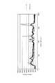
ここで、実施例では、測定システム1を用いて、微細流路デバイス100に流体を流す前の第1状態と、微細流路デバイス100に流体を流している間の第2状態とを測定し、それぞれの測定結果を比較することとした。 Here, in the embodiment, the
まず、第1状態の微細流路デバイス100として、参照モデル分子を付着させた嵌合部材120を有する微細流路デバイス100を作成した。参照モデル分子としては、トランス1,2ビス4ピリジルエチレン(通称、BPE)を用いた。具体的に、嵌合部材120をBPEの1mM溶液に浸漬し、その後、嵌合部材120を洗浄乾燥させた。また、乾燥後の嵌合部材120を、管部材110に嵌合させることで、微細流路デバイス100を作成した。 First, as the
そして、第1状態の微細流路デバイス100を、表面増強ラマン分光法によって測定した。 Then, the
次に、第1状態の微細流路デバイス100に対して、対象モデル分子を含む流体を流しながら、第2状態の微細流路デバイス100を測定した。具体的に、対象モデル分子であるp−アミノチオフェノール(通称、PATP)の1mM溶液を、流体として流しながら、表面増強ラマン分光法によってリアルタイムで測定した。 Next, the
図5には、測定システム1を用いて測定した測定結果を示すグラフが示されている。図5の縦軸はラマン信号強度を示し、横軸はラマンシフト(cm−1)を示す。 FIG. 5 shows a graph showing the measurement results measured using the
図5において、データX1は、微細流路デバイス100に流体を流さずに、参照モデル分子を付着させた第1状態の微細流路デバイス100を用いて、ラマンスペクトルを測定したデータである。 In FIG. 5, data X <b> 1 is data obtained by measuring a Raman spectrum using the
一方、図5において、データX2は、対象モデル分子であるPATPの1mM溶液を流体として流した第2状態の微細流路デバイス100を用いて、ラマンスペクトルをリアルタイムで測定したデータである。 On the other hand, in FIG. 5, data X2 is data obtained by measuring a Raman spectrum in real time using the
図5に示すように、データX1に見られたピークが、データX2では減少しており、データX1〜X2間のピークの変化を確認できる。特に、データX2では、PATPの特徴である1073cm−1付近のピークが検出できていることから、流体に含まれる物質をリアルタイムに測定できることが確認できた。 As shown in FIG. 5, the peak observed in the data X1 is decreased in the data X2, and the change of the peak between the data X1 and X2 can be confirmed. In particular, in data X2, since a peak around 1073 cm −1, which is a characteristic of PATP, can be detected, it has been confirmed that substances contained in the fluid can be measured in real time.
[変形例]
次に、上述した第1実施形態の変形例について説明する。上述した第1実施形態では、嵌合部材120の溝内面122に金属ナノ粒子Mが形成されていたが、これに限定されるものではない。例えば、嵌合部材120は、微細溝121の溝底部122bに固定される微小部材132を更に備え、金属ナノ粒子Mが、微小部材132の表面132aに形成されていてもよい。[Modification]
Next, a modification of the first embodiment described above will be described. In 1st Embodiment mentioned above, although the metal nanoparticle M was formed in the groove | channel
具体的に、図6(a)に示すように、微小部材132は、微細溝121の一部に形成される穴部131に埋め込まれることで、微細溝121の溝底部122bに固定されていてもよい。また、微小部材132は、微細溝121の一部に所定間隔を設けて複数配置されていてもよい。 Specifically, as shown in FIG. 6A, the
微小部材132は、嵌合部材120を貫通する構成であってもよい。また、微小部材132の固定方法は、接着剤を用いて固定してもよいし、穴部131に形成した雌ネジに、微小部材132に形成した雄ネジを締め込むことによって固定してもよい。 The
なお、微小部材132の形状は、円柱、四角柱、三角柱など、何れの柱状であってもよい。また、微小部材132の形状は、図6(b)に示すように、球状であってもよい。 The shape of the
また、微小部材132は、紐状であってもよい。この場合、紐状の微小部材132は、微細溝121の溝底部122bに沿って固定した状態で配置される。 Further, the
以上のように、嵌合部材120は、金属ナノ粒子Mを形成した微小部材132を別体で作成した上で、微細溝121に取り付ける構成であってもよい。 As described above, the
これにより、微小部材132に金属ナノ粒子Mをより確実に形成した上で、微細溝121に取り付けることができるので、金属ナノ粒子Mをより確実に形成した嵌合部材120を作成できる。よって、表面増強ラマン分光法を用いた測定方法により、ラマン散乱光L2をより確実に発光させることができ、この結果、測定精度を向上することができる。 Accordingly, the metal nanoparticles M can be more reliably formed on the
[本発明のその他の実施形態]
以上、上述の実施形態を用いて本発明について詳細に説明したが、当業者にとっては、本発明が本明細書中に説明した実施形態に限定されるものではないということは明らかである。[Other Embodiments of the Present Invention]
Although the present invention has been described in detail using the above-described embodiments, it is obvious to those skilled in the art that the present invention is not limited to the embodiments described in this specification.
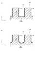
例えば、上述した第1実施形態では、微細溝121の断面形状は、V字形状である場合を例に挙げて説明したが、これに限定されるものではない。例えば、図7(a)〜(b)に示すように、微細溝121の断面形状は、コの字状、又は、U字形状あってもよい。すなわち、微細溝121の断面形状は、V字形状、U字形状、コの字状の何れであってもよい。又は、それらの組合せであってもよい。すなわち、V字形状、U字形状、コの字状の内の2つ以上を組合せた構成であってもよい。 For example, in the first embodiment described above, the case where the cross-sectional shape of the
例えば、微細溝121の断面形状が、コの字状、又は、U字形状である場合、V字形状に比べて、溝底部122bに底面を広く確保でき、この底面に金属ナノ粒子Mを形成できる。このため、発光器40から放出させる励起光L1が、金属ナノ粒子Mに照射されやすくなり、ラマン散乱光L2がより発光しやすくなる。 For example, when the cross-sectional shape of the
また、嵌合部材120の形状や微細溝121の形状は、様々な形状を適用できる。例えば、図8(a)に示すように、嵌合部材120が、円柱形状であって、嵌合部材120の外周部120aに、中心軸Axに沿って延びる微細溝121が形成されていてもよい。また、図8(b)に示すように、嵌合部材120が、円錐形状であって、嵌合部材120の外周部120aに、中心軸Axに沿って延びる微細溝121が形成されていてもよい。また、図8(c)に示すように、嵌合部材120が、卵形形状であって、嵌合部材120の外周部120aに、中心軸Axに沿って延びる微細溝121が形成されていてもよい。 Various shapes can be applied to the
或いは、図9(a)に示すように、嵌合部材120は、中空部125を有する筒形状であって、嵌合部材120の外周部120aの一部において、両端が中空部125に連通する微細溝121が形成される構成であってもよい。また、図9(b)に示すように、嵌合部材120の外周部120aに形成される微細溝121が、溝断面積が所定面積の第1微細溝121aと、溝断面積が所定面積よりも小さい第2微細溝121bとによって構成されていてもよい。なお、第1微細溝121aの溝断面積は、0.01mm2〜10mm2であり、第2微細溝121bの溝断面積は、100μm2〜0.1mm2であることが好ましい。Or as shown to Fig.9 (a), the
図9(a)〜(b)に示す嵌合部材120によれば、溝面積の小さい微細溝121及び第2微細溝121bを、嵌合部材120の外周部120aの一部にのみ形成するので、全部にわたって形成する場合に比べて、流体を搬送する際の流路抵抗を抑制することができる。 According to the
また、例えば、上述の実施形態では、管部材110の中空部111において、嵌合部材120が嵌合によってねじ込まれることで固定されていたが、これに限定されるものではない。例えば、嵌合部材120は、接着剤によって、管部材110の中空部111に固定されていてもよい。或いは、管部材110の外側から、管部材110と嵌合部材120とを挟み込む挟込部材を更に備えることで、嵌合部材120を固定してもよい。 For example, in the above-mentioned embodiment, in the
また、例えば、嵌合部材120を管部材110に嵌合する作業効率を高める観点から、嵌合部材120は、嵌合部材120のX方向の端部(端面)において、ドライバーなどの工具でねじ込むためのマイナス(−)溝又はプラス(+)溝が形成されていてもよい。 Further, for example, from the viewpoint of improving the working efficiency of fitting the
このように、本発明は上記実施の形態そのままに限定されるものではなく、実施段階ではその要旨を逸脱しない範囲で構成要素を変形して具体化できる。また、上記実施の形態に開示されている複数の構成要素の適宜な組み合せにより、種々の発明を形成できる。例えば、実施の形態に示される全構成要素から幾つかの構成要素を削除してもよい。 As described above, the present invention is not limited to the above-described embodiments as they are, and can be embodied by modifying the constituent elements without departing from the scope of the invention in the implementation stage. Various inventions can be formed by appropriately combining a plurality of constituent elements disclosed in the embodiments. For example, some components may be deleted from all the components shown in the embodiment.
本発明の微細流路デバイス及び測定方法は、流体に含まれる物質のリアルタイムモニタリング等に適用することができる。 The fine channel device and the measurement method of the present invention can be applied to real-time monitoring of a substance contained in a fluid.
1…測定システム
10…供給機
20,30…搬送管
100…微細流路デバイス
110…管部材
110a…内周部
111…中空部
120…嵌合部材
120a…外周部
121…微細溝
122…溝内面
122b…溝底部
123…外側端部
125…中空部
131…穴部
132…微小部材
M…金属ナノ粒子
DESCRIPTION OF
Claims (6)
Translated fromJapanese所定方向に沿って延びる中空部が形成される管部材と、
前記中空部に嵌合される嵌合部材と、を備え、
前記嵌合部材を覆っている前記管部材の少なくともラマン分光測定部分は、透明な部材で形成され、
前記嵌合部材の外周部には、前記管部材の内周部との間に前記微細流路を形成する微細溝が設けられており、
前記微細溝の溝内面には、表面増強ラマン分光測定用金属ナノ粒子が形成される
ことを特徴とする微細流路デバイス。A microchannel device comprising a microchannel for flowing a fluid, and used when measuring a substance contained in the fluid by surface-enhanced Raman spectroscopy,
A tube member formed with a hollow portion extending along a predetermined direction;
A fitting member fitted into the hollow part,
At least the Raman spectroscopic measurement part of the tube member covering the fitting member is formed of a transparent member,
The outer periphery of the fitting member is provided with a minute groove that forms the minute channel between the inner periphery of the tube member,
A microchannel device, wherein metal nanoparticles for surface enhanced Raman spectroscopy are formed on the inner surface of the microgroove.
ことを特徴とする請求項1記載の微細流路デバイス。The microchannel device according to claim 1, wherein the tube member is a hollow tube.
ことを特徴とする請求項1又は2に記載の微細流路デバイス。The fine channel device according to claim 1, wherein the fine groove is formed in a spiral shape on an outer peripheral portion of the fitting member.
ことを特徴とする請求項1乃至3の何れか一項に記載の微細流路デバイス。4. The fine structure according to claim 1, wherein a cross-sectional shape of the fine groove is any one of a V shape, a U shape, a U shape, or a combination thereof. 5. Channel device.
前記金属ナノ粒子は、前記微小部材の外表面に形成される
ことを特徴とする請求項1乃至4の何れか一項に記載の微細流路デバイス。The fitting member further includes a micro member fixed to a groove bottom of the micro groove,
5. The microchannel device according to claim 1, wherein the metal nanoparticles are formed on an outer surface of the micro member.
前記微細流路デバイスは、
所定方向に沿って延びる中空部が形成される管部材と、
前記中空部に嵌合される嵌合部材と、を備え、
前記嵌合部材を覆っている前記管部材の少なくともラマン分光測定部分は、透明な部材で形成され、
前記嵌合部材の外周部には、前記管部材の内周部との間に前記微細流路を形成する微細溝が形成されており、
前記微細溝の溝内面には、表面増強ラマン分光測定用金属ナノ粒子が形成される
ことを特徴とする測定方法。
Using a microchannel device having a microchannel for flowing a fluid, and measuring a substance contained in the fluid by surface-enhanced Raman spectroscopy,
The fine channel device is:
A tube member formed with a hollow portion extending along a predetermined direction;
A fitting member fitted into the hollow part,
At least the Raman spectroscopic measurement part of the tube member covering the fitting member is formed of a transparent member,
A fine groove that forms the fine flow path is formed between the outer peripheral portion of the fitting member and the inner peripheral portion of the pipe member,
A measurement method, wherein metal nanoparticles for surface-enhanced Raman spectroscopy are formed on the inner surface of the fine groove.
Priority Applications (1)
| Application Number | Priority Date | Filing Date | Title |
|---|---|---|---|
| JP2015177331AJP6583913B2 (en) | 2015-09-09 | 2015-09-09 | Fine channel device and measuring method |
Applications Claiming Priority (1)
| Application Number | Priority Date | Filing Date | Title |
|---|---|---|---|
| JP2015177331AJP6583913B2 (en) | 2015-09-09 | 2015-09-09 | Fine channel device and measuring method |
Publications (2)
| Publication Number | Publication Date |
|---|---|
| JP2017053702A JP2017053702A (en) | 2017-03-16 |
| JP6583913B2true JP6583913B2 (en) | 2019-10-02 |
Family
ID=58317779
Family Applications (1)
| Application Number | Title | Priority Date | Filing Date |
|---|---|---|---|
| JP2015177331AActiveJP6583913B2 (en) | 2015-09-09 | 2015-09-09 | Fine channel device and measuring method |
Country Status (1)
| Country | Link |
|---|---|
| JP (1) | JP6583913B2 (en) |
Family Cites Families (6)
| Publication number | Priority date | Publication date | Assignee | Title |
|---|---|---|---|---|
| JP4579593B2 (en)* | 2004-03-05 | 2010-11-10 | キヤノン株式会社 | Target substance recognition element, detection method and apparatus |
| JP2006144740A (en)* | 2004-11-24 | 2006-06-08 | Miraca Holdings Inc | Micropump, liquid supply apparatus, and liquid supply system |
| JP5870497B2 (en)* | 2011-03-18 | 2016-03-01 | セイコーエプソン株式会社 | Measuring apparatus and measuring method |
| US9272126B2 (en)* | 2011-04-29 | 2016-03-01 | The Board Of Trustees Of The University Of Illinois | Photonic biosensors incorporated into tubing, methods of manufacture and instruments for analyzing the biosensors |
| WO2012165400A1 (en)* | 2011-06-03 | 2012-12-06 | 株式会社日立ハイテクノロジーズ | Method and device for optical analysis of biopolymer |
| JP2015114219A (en)* | 2013-12-12 | 2015-06-22 | セイコーエプソン株式会社 | Electric field enhancement element, analyzer, and electronic device |
- 2015
- 2015-09-09JPJP2015177331Apatent/JP6583913B2/enactiveActive
Also Published As
| Publication number | Publication date |
|---|---|
| JP2017053702A (en) | 2017-03-16 |
Similar Documents
| Publication | Publication Date | Title |
|---|---|---|
| Haddad et al. | Detection and quantitation of trace fentanyl in heroin by surface-enhanced Raman spectroscopy | |
| Xu et al. | Detection of pesticide residues in food using surface-enhanced Raman spectroscopy: a review | |
| Zhong et al. | Porous silicon photonic crystals coated with Ag nanoparticles as efficient substrates for detecting trace explosives using SERS | |
| Que et al. | Highly Reproducible Surface‐Enhanced Raman Scattering on a Capillarity‐Assisted Gold Nanoparticle Assembly | |
| Zhao et al. | SERS-based ultrasensitive detection of organophosphorus nerve agents via substrate’s surface modification | |
| Alsammarraie et al. | Using standing gold nanorod arrays as surface-enhanced Raman spectroscopy (SERS) substrates for detection of carbaryl residues in fruit juice and milk | |
| He et al. | Use of a fractal-like gold nanostructure in surface-enhanced Raman spectroscopy for detection of selected food contaminants | |
| Quang et al. | A portable surface-enhanced Raman scattering sensor integrated with a lab-on-a-chip for field analysis | |
| Nguyen et al. | Use of graphene and gold nanorods as substrates for the detection of pesticides by surface enhanced Raman spectroscopy | |
| Pham et al. | 4-Mercaptobenzoic acid labeled gold-silver-alloy-embedded silica nanoparticles as an internal standard containing nanostructures for sensitive quantitative thiram detection | |
| Convertino et al. | Disordered array of Au covered Silicon nanowires for SERS biosensing combined with electrochemical detection | |
| Zhao et al. | Unveiling practical considerations for reliable and standardized SERS measurements: lessons from a comprehensive review of oblique angle deposition-fabricated silver nanorod array substrates | |
| Liu et al. | Detection of pesticides in fruits by surface-enhanced Raman spectroscopy coupled with gold nanostructures | |
| EP2771658B1 (en) | Apparatus for use in a sensing application having a destructible cover | |
| Yazdi et al. | Multiplexed detection of aquaculture fungicides using a pump-free optofluidic SERS microsystem | |
| Litti et al. | Detection of low-quantity anticancer drugs by surface-enhanced Raman scattering | |
| US9678014B2 (en) | Capillary flow plasmonic sensor | |
| JP6583913B2 (en) | Fine channel device and measuring method | |
| Buja et al. | Microfluidic setup for on-line SERS monitoring using laser induced nanoparticle spots as SERS active substrate | |
| Lee et al. | A low-cost, highly-stable surface enhanced Raman scattering substrate by Si nanowire arrays decorated with Au nanoparticles and Au backplate | |
| US9134249B2 (en) | Electric field generating apparatus for performing spectroscopy | |
| Visaveliya* et al. | Microflow SERS measurements using sensing particles of polyacrylamide/silver composite materials | |
| CN103822912A (en) | Super hydrophobic type SERS (Surface-enhanced Raman scattering) composite substrate | |
| JP2007513345A5 (en) | ||
| Liu et al. | A tunable freeform-segmented reflector in a microfluidic system for conventional and surface-enhanced raman spectroscopy |
Legal Events
| Date | Code | Title | Description |
|---|---|---|---|
| A621 | Written request for application examination | Free format text:JAPANESE INTERMEDIATE CODE: A621 Effective date:20180709 | |
| TRDD | Decision of grant or rejection written | ||
| A01 | Written decision to grant a patent or to grant a registration (utility model) | Free format text:JAPANESE INTERMEDIATE CODE: A01 Effective date:20190806 | |
| A61 | First payment of annual fees (during grant procedure) | Free format text:JAPANESE INTERMEDIATE CODE: A61 Effective date:20190829 | |
| R150 | Certificate of patent or registration of utility model | Ref document number:6583913 Country of ref document:JP Free format text:JAPANESE INTERMEDIATE CODE: R150 | |
| R250 | Receipt of annual fees | Free format text:JAPANESE INTERMEDIATE CODE: R250 | |
| R250 | Receipt of annual fees | Free format text:JAPANESE INTERMEDIATE CODE: R250 |