JP6582133B2 - In-vehicle control device - Google Patents
In-vehicle control deviceDownload PDFInfo
- Publication number
- JP6582133B2 JP6582133B2JP2018528445AJP2018528445AJP6582133B2JP 6582133 B2JP6582133 B2JP 6582133B2JP 2018528445 AJP2018528445 AJP 2018528445AJP 2018528445 AJP2018528445 AJP 2018528445AJP 6582133 B2JP6582133 B2JP 6582133B2
- Authority
- JP
- Japan
- Prior art keywords
- current
- control device
- voltage
- diode
- input terminal
- Prior art date
- Legal status (The legal status is an assumption and is not a legal conclusion. Google has not performed a legal analysis and makes no representation as to the accuracy of the status listed.)
- Active
Links
Images


Classifications
- B—PERFORMING OPERATIONS; TRANSPORTING
- B60—VEHICLES IN GENERAL
- B60R—VEHICLES, VEHICLE FITTINGS, OR VEHICLE PARTS, NOT OTHERWISE PROVIDED FOR
- B60R16/00—Electric or fluid circuits specially adapted for vehicles and not otherwise provided for; Arrangement of elements of electric or fluid circuits specially adapted for vehicles and not otherwise provided for
- B60R16/02—Electric or fluid circuits specially adapted for vehicles and not otherwise provided for; Arrangement of elements of electric or fluid circuits specially adapted for vehicles and not otherwise provided for electric constitutive elements
- B60R16/03—Electric or fluid circuits specially adapted for vehicles and not otherwise provided for; Arrangement of elements of electric or fluid circuits specially adapted for vehicles and not otherwise provided for electric constitutive elements for supply of electrical power to vehicle subsystems or for
- B60R16/033—Electric or fluid circuits specially adapted for vehicles and not otherwise provided for; Arrangement of elements of electric or fluid circuits specially adapted for vehicles and not otherwise provided for electric constitutive elements for supply of electrical power to vehicle subsystems or for characterised by the use of electrical cells or batteries
- G—PHYSICS
- G01—MEASURING; TESTING
- G01R—MEASURING ELECTRIC VARIABLES; MEASURING MAGNETIC VARIABLES
- G01R19/00—Arrangements for measuring currents or voltages or for indicating presence or sign thereof
- G01R19/165—Indicating that current or voltage is either above or below a predetermined value or within or outside a predetermined range of values
- G—PHYSICS
- G01—MEASURING; TESTING
- G01R—MEASURING ELECTRIC VARIABLES; MEASURING MAGNETIC VARIABLES
- G01R31/00—Arrangements for testing electric properties; Arrangements for locating electric faults; Arrangements for electrical testing characterised by what is being tested not provided for elsewhere
- G01R31/50—Testing of electric apparatus, lines, cables or components for short-circuits, continuity, leakage current or incorrect line connections
- G01R31/66—Testing of connections, e.g. of plugs or non-disconnectable joints
- G01R31/67—Testing the correctness of wire connections in electric apparatus or circuits
- H—ELECTRICITY
- H02—GENERATION; CONVERSION OR DISTRIBUTION OF ELECTRIC POWER
- H02H—EMERGENCY PROTECTIVE CIRCUIT ARRANGEMENTS
- H02H1/00—Details of emergency protective circuit arrangements
- H02H1/0007—Details of emergency protective circuit arrangements concerning the detecting means
- H—ELECTRICITY
- H02—GENERATION; CONVERSION OR DISTRIBUTION OF ELECTRIC POWER
- H02H—EMERGENCY PROTECTIVE CIRCUIT ARRANGEMENTS
- H02H3/00—Emergency protective circuit arrangements for automatic disconnection directly responsive to an undesired change from normal electric working condition with or without subsequent reconnection ; integrated protection
- H02H3/18—Emergency protective circuit arrangements for automatic disconnection directly responsive to an undesired change from normal electric working condition with or without subsequent reconnection ; integrated protection responsive to reversal of direct current
Landscapes
- Physics & Mathematics (AREA)
- General Physics & Mathematics (AREA)
- Engineering & Computer Science (AREA)
- Mechanical Engineering (AREA)
- Measurement Of Current Or Voltage (AREA)
- Testing Of Short-Circuits, Discontinuities, Leakage, Or Incorrect Line Connections (AREA)
- Electronic Switches (AREA)
- Charge And Discharge Circuits For Batteries Or The Like (AREA)
- Direct Current Feeding And Distribution (AREA)
Description
Translated fromJapanese本発明は、自動車等に搭載される車載制御装置に関する。 The present invention relates to an in-vehicle control device mounted on an automobile or the like.
自動車等に搭載されるECU(Electronic Control Unit)などの電子機器は、車両に搭載されたバッテリから供給される電流を用いて動作しているが、バッテリに充電されている電力はある程度限られているため、電子機器の通常動作時における消費電力のほかに、省電力状態に移行した場合の消費電流(いわゆる暗電流)についても管理・削減していくことが求められている。 Electronic devices such as ECUs (Electronic Control Units) mounted on automobiles and the like operate using current supplied from a battery mounted on the vehicle, but the power charged in the battery is limited to some extent. Therefore, in addition to the power consumption during normal operation of the electronic device, it is required to manage and reduce the current consumption (so-called dark current) when shifting to the power saving state.
そこで、このような暗電流に関する技術として、例えば、特許文献1(特開2015−95086号公報)には、所定の条件により、複数の電子機器が行う動作をそれぞれ制御する稼働状態と、前記制御を休止する省電力状態とに移行可能な所定数の制御装置と、前記各制御装置に供給する電流をそれぞれ監視し制御する監視制御手段と、前記各制御装置の稼働状態において、各制御装置に流れる電流を検出する第1の検出手段と、前記監視制御手段の制御により、前記各制御装置の稼働状態において前記各制御装置に駆動電流を供給し、前記第1の検出手段で所定の閾値を超える電流が検出されたときには前記各制御装置への駆動電流を遮断する第1の電流制御手段と、前記監視制御手段の制御により、前記各制御装置の省電力状態において、前記第1の電流制御手段から切り換えられて前記各制御装置に暗電流を供給し、前記各制御装置の稼働状態において前記各制御装置への暗電流を遮断する第2の電流制御手段と、前記各制御装置の省電力状態において、前記暗電流の変化に基づく電圧降下量を検出する第2の検出手段と、前記第2の検出手段により所定の電圧降下量が検出されたか否かに基づいて、前記制御装置の省電力状態の異常の有無を判定する異常判定手段とを備えた電源制御システムが開示されている(特許請求の範囲請求項1参照)。
Therefore, as a technique relating to such dark current, for example, Patent Document 1 (JP 2015-95086 JP), a predetermined condition, and the operating state controlling operation in which a plurality of electronic devices perform each said A predetermined number of control devices capable of transitioning to a power saving state in which control is suspended; monitoring control means for monitoring and controlling currents supplied to the control devices; and control devices in the operating states of the control devices. The first detection means for detecting the current flowing through the control device and the control of the monitoring control means supply a drive current to each control device in the operating state of each control device, and the first detection means provides a predetermined threshold value. When a
しかしながら、上記従来技術においては、ECUの外部に暗電流の異常を検出するための回路や暗電流の異常を検出されたECUを特定するための回路(すなわち、暗電流の異常を検出するためのECUなど)を別途設ける必要があるために回路規模が大きくなってしまうという問題点があった。また、上記従来技術では、制御不能により省電力状態にならなかったことを暗電流の異常として検出するものであるため、暗電流自体の微小な変化を検出することができなかった。 However, in the above prior art, a circuit for detecting an abnormality in dark current outside the ECU and a circuit for specifying an ECU in which abnormality in dark current is detected (that is, for detecting an abnormality in dark current) There is a problem that the circuit scale becomes large because it is necessary to separately provide an ECU or the like. Further, in the above prior art, since it is detected as an abnormality of the dark current that the power saving state is not achieved due to the inability to control, it is impossible to detect a minute change in the dark current itself.
本発明は上記に鑑みてなされたものであり、回路規模の増加を抑制しつつ暗電流の異常を検出することができる車載制御装置を提供することを目的とする。 The present invention has been made in view of the above, and an object of the present invention is to provide an in-vehicle control device that can detect dark current abnormality while suppressing an increase in circuit scale.
上記目的を達成するために、本発明は、バッテリから電源入力端子を介して供給される電流により動作する負荷部と、前記電源入力端子と前記負荷部とを接続する電源経路上に配置され、前記電源入力端子に対する前記バッテリの逆接続時の逆電流を防止する逆接保護素子と、前記逆接保護素子の前記電源入力端子側の電圧と前記負荷部側の電圧の電圧差に基づいて、前記逆接保護素子に流れる電流の異常を検出する電流異常検出部とを備えたものとする。 In order to achieve the above object, the present invention is disposed on a power supply path that connects the power supply input terminal and the load section, a load section that operates by a current supplied from a battery via a power supply input terminal, A reverse connection protection element for preventing reverse current when the battery is reversely connected to the power input terminal, and the reverse connection based on a voltage difference between the voltage on the power input terminal side of the reverse connection protection element and the voltage on the load portion side. It is assumed that a current abnormality detection unit that detects abnormality of the current flowing through the protection element is provided.
回路規模の増加を抑制しつつ暗電流の異常を検出することができる。 An abnormal dark current can be detected while suppressing an increase in circuit scale.
以下、本発明の実施の形態を図面を参照しつつ説明する。 Hereinafter, embodiments of the present invention will be described with reference to the drawings.
<第1の実施の形態>
本発明の第1の実施の形態を図1〜図3を参照しつつ詳細に説明する。<First Embodiment>
A first embodiment of the present invention will be described in detail with reference to FIGS.
図1は、本実施の形態に係る車載制御装置を周辺構成とともに概略的に示す図である。 FIG. 1 is a diagram schematically showing the in-vehicle control device according to the present embodiment together with the peripheral configuration.
図1において、車載制御装置(ECU:Electronic Control Unit)100は、車両に搭載される種々の制御機能を有する複数の車載制御装置の1つであり、外部電源であるバッテリ10から電源入力端子100aを介して供給される電流により動作する負荷部としての制御装置2と、電源入力端子100aと制御装置2の間を流れる電流を監視する電流監視装置1とから概略構成されている。また、車載制御装置100は、接地端子(GND端子)100bを有している。 In FIG. 1, an in-vehicle control device (ECU: Electronic Control Unit) 100 is one of a plurality of in-vehicle control devices mounted on a vehicle and having various control functions, and includes a
制御装置2は、制御回路(マイコン等)や電源回路、ドライバなどにより構成されており、図示しない入出力端子等を介して車載制御装置100の外部(他の車載制御装置や制御対象など)と種々の情報(信号等)の授受を行うことによって、車載制御装置100が搭載される車両において車載制御装置100に割り当てられた制御機能を果たしている。 The
電流監視装置1は、電源入力端子100aに接続される電源の極性の誤り(いわゆる電源の逆接続)などから車載制御装置100の内部の回路を保護する逆接保護機能と、制御装置2の動作停止時(いわゆるスタンバイ時)において電源入力端子100aから制御装置2に流れる電流(暗電流)の異常を検出する(電流異常検出処理を行う)電流異常検出機能とを有している。電流監視装置1における電流異常検出処理の結果は、車載制御装置100の外部に電流異常検出結果信号3として出力され、電流監視装置1で検出される電流の状態(つまり、電源入力端子100aから入力される電流や制御装置2で用いられる電流の正常状態や異常状態)に応じて種々の処理を行う他の処理部(図示せず)で用いられる。 The
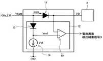
図2は、電流監視装置の構成を制御装置とともに概略的に示す図である。 FIG. 2 is a diagram schematically showing the configuration of the current monitoring device together with the control device.
図2において、電流監視装置1は、電源入力端子100aと制御装置2とを接続する電源経路上に配置されたダイオード11と、ダイオード11の両端の電位差に基づいて、電源入力端子100aから制御装置2に流れる電流(暗電流)の異常を検出する電流異常検出回路12とを備えている。 In FIG. 2, the
ダイオード11は、アノード側を電源入力端子100a側に接続し、カソード側を制御装置2側に接続した状態で配置されており、逆バイアス時、すなわち、電源入力端子100aへの電源の逆接続時に内部回路を保護する逆接保護機能、或いは、マイナスサージ保護機能を果たしている。 The
電流異常検出回路12は、ダイオード11のアノード側(電源入力端子100a側)にアノード側を接続したダイオード13と、ダイオード13のカソード側とGNDの間に接続され、ダイオード13からGNDに予め定めた一定の電流(基準電流Iref)が流れるように調整する基準電流源14と、ダイオード11のカソード側(制御装置2側)の電圧(電圧VB)とダイオード13のカソード側の電圧(基準電圧Vref)とを入力し、その比較結果を出力する比較回路15とを備えている。 The current
比較回路15は、制御装置2の動作停止時(スタンバイ時)において、基準電圧Vrefよりもダイオード11のカソード側の電圧VBの方が高い場合には、ダイオード11を流れる電流(暗電流)が正常値であるとする検出結果(電流異常検出結果信号3)としてLow信号(例えばGND電圧)を出力する。また、比較回路15は、制御装置2の動作停止時(スタンバイ時)において、基準電圧Vrefよりもダイオード11のカソード側の電圧VBの方が低い場合には、ダイオード11を流れる電流(暗電流)が異常値であるとする検出結果(電流異常検出結果信号3)としてHigh信号(例えば車載制御装置100の電源電圧)を出力する。 When the
言い換えると、比較回路15は、ダイオード11に流れる電流による電圧降下とダイオード13に流れる電流による電圧降下とを比較しているといえる。したがって、例えば、ダイオード11とダイオード13に同種のダイオードを用いた場合には、ダイオード11を流れる暗電流が基準電流Irefよりも多いか少ないかによって暗電流の異常を判定する、すなわち、基準電流Irefが暗電流の基準値となるよう単純化して考えることができる。なお、ダイオード11とダイオード13に同種同一ロットのIC(素子)を用いたり、ダイオード11とダイオード13を同一半導体素子中の近傍に形成したりすることによって、温度特性や特性バラツキの影響を抑えることができ、安定して暗電流の異常検出を行うことができる。 In other words, it can be said that the
なお、電流異常検出回路12による暗電流の異常の検出(電流異常検出処理)を間欠的に行うように構成しても良く、電流異常検出処理を行わない時は基準電流源14や比較回路15の動作を停止して電流の消費を抑えることができる。 Note that dark current abnormality detection (current abnormality detection processing) by the current
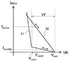
図3は、電源入力端子と制御装置とを接続する電源経路上に配置されたダイオードの両端間の電圧(電位差)と流れる電流との関係の一例を模式的に示す図であり、縦軸に電流、横軸に電圧をそれぞれ示している。 FIG. 3 is a diagram schematically showing an example of the relationship between the voltage (potential difference) between both ends of a diode arranged on the power supply path connecting the power supply input terminal and the control device, and the flowing current. Current and voltage are shown on the horizontal axis.
図3において、ダイオード11に流れる電流をIecu、ダイオード11のカソード側の電圧をVBとし、バッテリ10の電圧をVbattとすると、制御装置2での電力消費が無い場合はダイオード11を流れる電流Iecu及び電圧降下が0となるので電圧VB=Vbattとなり、制御装置2での電力消費が増加するに従ってダイオード11を流れる電流Iecu及び電圧降下が増加し、電圧Vbattと電圧VBとの差(すなわち、ダイオード11の両端電圧)が順電圧VFを超えると電流Iecuが急激に増加する。なお、図3においては、制御装置2の動作時(いわゆるアクティブ時)の電流をIactive、動作停止時(スタンバイ時)の電流をIstandbyとしてそれぞれ例示している。このように、VF>Vbatt−VBの範囲においては、微小電流である電流Iecuの微小な変化に対して電圧変化の感度が大きいため、基準電圧VrefをVF>Vbatt−Vrefの範囲に設定することにより、ダイオード11を流れる暗電流の高精度な検出が可能である。 In FIG. 3, assuming that the current flowing through the
なお、制御装置2の動作時(アクティブ時)においては、基準電流Irefを制御・変更することによって基準電圧VrefをVref≦Bbatt−VBとなるように変更し、制御装置2の動作時(アクティブ時)の異常電流を検出することができる。 During the operation of the control device 2 (when active), the reference voltage Vref is changed to satisfy Vref ≦ Bbatt−VB by controlling and changing the reference current Iref, and when the
以上の様に構成した本実施の形態の作用効果を説明する。 The effect of this Embodiment comprised as mentioned above is demonstrated.
従来技術においては、ECUの外部に暗電流の異常を検出するための回路や暗電流の異常を検出されたECUを特定するための回路(すなわち、暗電流の異常を検出するためのECUなど)を別途設ける必要があるために回路規模が大きくなってしまうという問題点があった。また、制御不能により省電力状態にならなかったことを暗電流の異常として検出するものであるため、暗電流自体の微小な変化を検出することができなかった。 In the prior art, a circuit for detecting an abnormality in the dark current outside the ECU and a circuit for specifying the ECU in which the abnormality in the dark current is detected (that is, an ECU for detecting the abnormality in the dark current). Therefore, there is a problem that the circuit scale becomes large. Further, since it is detected as an abnormality of the dark current that the power saving state has not been achieved due to the inability to control, a minute change in the dark current itself could not be detected.
これに対して本実施の形態においては、バッテリ10から電源入力端子100aを介して供給される電流Iecuにより動作する負荷部としての制御装置2と、電源入力端子100aと制御装置2とを接続する電源経路上に配置され、電源入力端子100aに対するバッテリ10の逆接続時の逆電流を防止する逆接保護素子としてのダイオード11と、ダイオード11の電源入力端子100a側の電圧Vbattと制御装置2側の電圧VBの電圧差に基づいて、ダイオード11に流れる電流の異常を検出する電流異常検出回路12とを備えるように構成した。 On the other hand, in the present embodiment,
逆接保護素子は、車載制御装置の電源入力端子に設けられる重要な機能を果たすものであるため車載制御装置に搭載されることが多いものであるところ、この逆接保護素子の両端電圧を用いて暗電流の異常を検出する本実施の形態においては、回路の増加を抑制しつつ暗電流の異常を検出することができる。 Since the reverse connection protection element performs an important function provided at the power input terminal of the in-vehicle control device, it is often mounted in the in-vehicle control device. In the present embodiment in which an abnormality in current is detected, an abnormality in dark current can be detected while suppressing an increase in circuits.
また、暗電流の異常を検出するために別途ECU等を用意する必要がないため、回路の増加抑制にさらに貢献することができる。 In addition, since it is not necessary to prepare a separate ECU or the like in order to detect dark current abnormality, it is possible to further contribute to the suppression of circuit increase.
また、各車載制御装置に設けられる逆接保護素子としてダイオードを用いるように構成したので、ECUごとに暗電流の異常を高精度に検出することができる。 Moreover, since it comprised so that a diode might be used as a reverse connection protection element provided in each vehicle-mounted control apparatus, abnormality of dark current can be detected with high precision for every ECU.
<第2の実施の形態>
本発明の第2の実施の形態を図4〜図6を参照しつつ詳細に説明する。<Second Embodiment>
A second embodiment of the present invention will be described in detail with reference to FIGS.
本実施の形態は、第1の実施の形態の電流監視装置において逆接保護素子として示したダイオードに代えて、MOSFET(Metal-Oxide-Semiconductor Field-Effect Transistor)を用いた場合を示すものである。 In the present embodiment, a MOSFET (Metal-Oxide-Semiconductor Field-Effect Transistor) is used instead of the diode shown as the reverse connection protection element in the current monitoring apparatus of the first embodiment.
図4は、本実施の形態に係る電流監視装置の構成を制御装置とともに概略的に示す図である。図中、第1の実施の形態と同様の部材には同じ符号を付し、説明を省略する。 FIG. 4 is a diagram schematically showing the configuration of the current monitoring device according to the present embodiment together with the control device. In the figure, the same members as those in the first embodiment are denoted by the same reference numerals, and description thereof is omitted.
図4において、電流監視装置1Aは、電源入力端子100aに接続される電源の極性の誤り(いわゆる電源の逆接続)などから車載制御装置100の内部の回路を保護する逆接保護機能と、制御装置2の動作時(いわゆるアクティブ時)および動作停止時(いわゆるスタンバイ時)において電源入力端子100aから制御装置2に流れる電流(動作電流/暗電流)の異常を検出する(電流異常検出処理を行う)電流異常検出機能とを有しており、電流異常検出処理の結果を車載制御装置100の外部に電流異常検出結果信号3として出力する。 In FIG. 4, the
電流監視装置1Aは、電源入力端子100aと制御装置2とを接続する電源経路上に配置されたMOSFET21と、MOSFET21の両端の電位差に基づいて、電源入力端子100aから制御装置2に流れる電流の異常を検出する電流異常検出回路22とを備えている。 The current monitoring device 1A has an abnormality in the current flowing from the
MOSFET21は、その内部に形成されるボディダイオード21a(寄生ダイオードや内蔵ダイオードとも言う)のアノード側が電源入力端子100a側に接続され、カソード側が制御装置2側に接続されるように配置されており、このボディダイオード21aは逆バイアス時、すなわち、電源入力端子100aへの電源の逆接続時に内部回路を保護する逆接保護機能、或いは、マイナスサージ保護機能を果たしている。MOSFET21は、他の処理部(例えば、制御装置2や車載制御装置100の外部にある処理部)からゲートに入力される制御信号(ゲート信号)Vgにより、遮断状態(電流を流さない状態)と導通状態(電流を流す状態)とを切り換えられる。制御装置2のアクティブ時には、MOSFET21を導通状態に切り換えるON信号が制御信号VgとしてMOSFET21のゲートに入力され、スタンバイ時には、MOSFET21を遮断状態に切り換えるOFF信号が制御信号VgとしてMOSFET21のゲートに入力される。 The
電流異常検出回路22は、MOSFET21の電源入力端子100a側(言い換えるとボディダイオード21aのアノード側)の電圧に基づいて基準電圧Vrefを設定する基準電圧設定部14Aと、MOSFET21の制御装置2側(言い換えるとボディダイオード21aのカソード側)の電圧(電圧VB)と基準電圧Vrefとを入力し、その比較結果を出力する比較回路15とを備えている。 The current
比較回路15は、基準電圧VrefよりもMOSFET21の電源入力端子100a側(ボディダイオード21aのアノード側)の電圧VBの方が高い場合には、MOSFET21やボディダイオード21aを流れる電流(動作電流/暗電流)が正常値であるとする検出結果(電流異常検出結果信号3)としてLow信号(例えばGND電圧)を出力する。また、比較回路15は、基準電圧VrefよりもMOSFET21の電源入力端子100a側(ボディダイオード21aのアノード側)の電圧VBの方が低い場合には、MOSFET21やボディダイオード21aを含む)を流れる電流(動作電流/暗電流)が異常値であるとする検出結果(電流異常検出結果信号3)としてHigh信号(例えば車載制御装置100の電源電圧)を出力する。 When the voltage VB on the
基準電圧設定部14Aは、MOSFET21の制御信号Vgを取得しており、MOSFET21が導通状態に制御されるON信号が入力された場合には、制御装置2がアクティブである場合の基準電圧Vref(特に基準電圧Vrefonと称する)を比較回路15に出力し、MOSFET21が遮断状態に制御されるOFF信号が入力された場合には、制御装置2がスタンバイである場合の基準電圧(特に基準電圧Vrefoffと称する)を比較回路15に出力する。 The reference
図5は、MOSFETの両端間の電圧(電位差)と流れる電流との関係の一例を模式的に示す図であり、縦軸に電流、横軸に電圧をそれぞれ示している。 FIG. 5 is a diagram schematically illustrating an example of the relationship between the voltage (potential difference) between both ends of the MOSFET and the flowing current, where the vertical axis indicates current and the horizontal axis indicates voltage.
図5においては、MOSFET21(ボディダイオード21aを含む)に流れる電流をIecu、MOSFET21の制御装置2側(ボディダイオード21aのカソード側)の電圧をVBとし、MOSFET21の電源入力端子100a側(ボディダイオード21aのアノード側)に入力されるバッテリ10の電圧をVbattとする。 In FIG. 5, the current flowing through the MOSFET 21 (including the
制御装置2がアクティブ状態であってMOSFET21の制御信号VgがON信号である場合は、MOSFET21は導通状態(低抵抗状態)となるので、ボディダイオード21aはOFF領域で動作する状態となる。したがって、図5に実線50で示すように、制御装置2での電力消費が無い場合はMOSFET21を流れる電流Iecu及び電圧降下が0となるので電圧VB=Vbattとなり、制御装置2での電力消費が増加するに従ってMOSFET21を流れる電流Iecu及び電圧降下が増加していく。図5においては、制御装置2のアクティブ時の電流をIactiveとして例示している。 When the
そして、制御装置2がアクティブ状態であってMOSFET21の制御信号VgがON信号である場合に基準電圧Vref(Vrefon)を設定することにより、MOSFET21を流れる動作電流の検出が可能である。なお、MOSFET21による電圧降下によってボディダイオード21aがON状態となる場合は考えないものとし、基準電圧Vrefonは、VF>Vbatt−Vrefonの範囲(ボディダイオード21aがONしない範囲)に設定するものとする。 When the
また、制御装置2がスタンバイ状態であってMOSFET21の制御信号VgがOFF信号である場合は、MOSFET21は遮断状態(高抵抗状態)となるので、ボディダイオード21aが主として動作する状態となる。すなわち、図5に実線51で示すように、制御装置2での電力消費が無い場合はボディダイオード21aを流れる電流Iecu及び電圧降下が0となるので電圧VB=Vbattとなり、制御装置2での電力消費が増加するに従ってボディダイオード21aを流れる電流Iecu及び電圧降下が増加し、電圧Vbattと電圧VBとの差(すなわち、ボディダイオード21aの両端電圧)が順電圧VFを超えると電流Iecuが急激に増加する。図5においては、制御装置2のスタンバイ時の電流をIstandbyとして例示している。 Further, when the
そして、VF>Vbatt−VBの範囲、すなわち、微小電流である電流Iecuの微小な変化に対して電圧変化の感度が大きい範囲においては、基準電圧Vref(Vrefoff)をVF>Vbatt−Vrefoffの範囲に設定することにより、ボディダイオード21aを流れる暗電流の高精度な検出が可能である。 In the range of VF> Vbatt−VB, that is, in the range where the sensitivity of the voltage change is large with respect to the minute change of the current Iecu, which is a minute current, the reference voltage Vref (Vrefoff) is set to the range of VF> Vbatt−Vrefoff. By setting, the dark current flowing through the
その他の構成は第1の実施の形態と同様である。 Other configurations are the same as those of the first embodiment.
以上のように構成した本実施の形態においても第1の実施の形態と同様の効果を得ることができる。 In the present embodiment configured as described above, the same effects as those of the first embodiment can be obtained.
また、本実施の形態においてはさらに以下のような作用効果を得ることができる。 Further, in the present embodiment, the following operational effects can be obtained.
図6は、本実施の形態における制御装置2の構成の一例を概略的に示す図である。 FIG. 6 is a diagram schematically showing an example of the configuration of the
図6において、制御装置2は、制御回路としてのマイコン61と、電流監視装置1を介して制御装置2に入力される電圧VBを監視する電圧監視部66と、電流監視装置1を介して制御装置2に入力される電力を用いて動作する電源回路としての内部電源64と、電流監視装置1を介して制御装置2のマイコン61に入力される電流の過電流を検出して防止する過電流検出部63と、内部電源64の電圧から過電流検出部63で用いる参照電圧を生成する参照電圧生成部65と、マイコン61に入力される電圧の変動を抑制するデカップリングコンデンサ62とから概略構成されている。また、電流監視装置1と制御装置2の間には、電流監視装置1から制御装置2に入力される電圧の変動を抑制するデカップリングコンデンサ4が配置されている。 In FIG. 6, the
すなわち、本実施の形態においては、制御装置2のマイコン61の故障やデカップリングコンデンサ62の短絡などによって生じる過電流を防止する過電流検出部63に加えて、電流監視装置1によって過電流を防止することができるので、過電流検出機能の二重化を図ることができ、過電流検出機能の信頼性を向上することができる。また、例えば、過電流検出機能を有しない制御装置においても過電流検出機能を提供することができ、信頼性を向上することができる。 That is, in the present embodiment, the
また、例示した制御装置2においては、制御装置2の電源の入力部に配置されるデカップリングコンデンサ4は過電流検出部63の上流側に配置されるため、過電流検出部63によるデカップリングコンデンサ4の短絡を検出することが出来ないが、電流監視装置1によって、制御装置2のアクティブ時にはデカップリングコンデンサ4の短絡を検出することができるとともに、制御装置2のスタンバイ時には制御装置2の電圧監視部66や内部電源64、参照電圧生成部65等の微小リーク(暗電流)を監視して異常発生時には検出することができるため、信頼性を向上することができる。 In the illustrated
<第3の実施の形態>
本発明の第3の実施の形態を図7及び図8を参照しつつ詳細に説明する。<Third Embodiment>
A third embodiment of the present invention will be described in detail with reference to FIGS.
本実施の形態は、第2の実施の形態においてMOSFETの診断機能を設けた場合を示すものである。 This embodiment shows a case where a MOSFET diagnosis function is provided in the second embodiment.
図7は、本実施の形態に係る車載制御装置を周辺構成とともに概略的に示す図である。図中、第1及び第2の実施の形態と同様の部材には同じ符号を付し、説明を省略する。 FIG. 7 is a diagram schematically showing the in-vehicle control device according to the present embodiment together with the peripheral configuration. In the drawing, members similar to those in the first and second embodiments are denoted by the same reference numerals, and description thereof is omitted.
図7において、車載制御装置100Aは、車両に搭載される種々の制御機能を有する複数の車載制御装置の1つであり、外部電源であるバッテリ10から電源入力端子100aを介して供給される電流により動作する負荷部としての制御装置2と、電源入力端子100aと制御装置2の間を流れる電流を監視する電流監視装置1と、電流監視装置1のMOSFET21の診断処理を行う診断装置7とから概略構成されている。また、車載制御装置100Aは、接地端子(GND端子)100bを有している。 In FIG. 7, an in-
診断装置7は、車載制御装置100Aの外部からの制御信号(図示せず)に基づいて、電流監視装置1のMOSFET21の制御信号Vgを出力してON/OFF制御を行うとともに、MOSFET21が正常であるかどうかを診断する診断処理を行うものである。 The
図8は、診断装置における診断処理時の各信号および電圧の変化を示す図であり、縦軸に電圧等の状態、横軸に時間を示している。なお、図8では、MOSFET21が正常に動作する場合を例示している。 FIG. 8 is a diagram illustrating changes in each signal and voltage during diagnostic processing in the diagnostic apparatus, where the vertical axis indicates the state of voltage and the horizontal axis indicates time. FIG. 8 illustrates the case where the
図8において、制御装置2がスタンバイ状態である場合には、電流Iecuは微小である。また、診断装置7はMOSFET21の制御信号Vgを制御してMOSFET21をOFF状態とする。このとき、DET信号(電流異常検出結果信号3)はLow信号(正常)となる。 In FIG. 8, when the
続いて、診断処理として、制御装置2がスタンバイ状態からアクティブ状態になった場合には、電流Iecuは動作電流となる。この電流はボディダイオード21aがONすることにより供給される。また、診断装置7はMOSFET21の制御信号Vgを制御してMOSFET21をOFF状態のままにする。このとき、DET信号(電流異常検出結果信号3)はHigh信号となる。ただし、このとき(診断処理中)のDET信号は、MOSFET21(又はボディダイオード21a)を流れる電流(暗電流)が異常値である場合のもととは扱わない。 Subsequently, as diagnostic processing, when the
続いて、診断装置7はMOSFET21の制御信号Vgを制御してMOSFET21をON状態に切り換える。このとき、DET信号(電流異常検出結果信号3)はLow信号となる。 Subsequently, the
このように、診断処理において、制御装置2のアクティブ時にMOSFET21をOFF状態に制御してDET信号(電流異常検出結果信号3)がHighとなることで、MOSFET21が正しくOFF状態となっていることが診断できる。 Thus, in the diagnostic processing, when the
なお、診断処理の時間(ボディダイオード21aがON状態となる時間)は、MOSFETのボディダイオードの特性を考慮して、十分に短くなるように設定する。車載制御装置等の電源に適用する電流監視装置には大サイズのMOSFETが用いられるためそのボディダイオードも十分に大きく、ボディダイオードがON状態となっても正常に動作する時間内で診断処理を行う十分な時間を確保することができる。 Note that the diagnosis processing time (the time during which the
また、本実施の形態では、制御装置2がスタンバイ状態からアクティブ状態に移行するときに診断処理を実施する場合を例示したが、アクティブ状態からスタンバイ状態に行こうする場合や、アクティブ状態中、スタンバイ状態中などに診断処理を実施しても良い。 In the present embodiment, the case where the
その他の構成は第1及び第2の実施の形態と同様である。 Other configurations are the same as those of the first and second embodiments.
以上のように構成した本実施の形態においても第1及び第2の実施の形態と同様の効果を得ることができる。 In the present embodiment configured as described above, the same effects as those of the first and second embodiments can be obtained.
また、MOSFETが正常に動作しているかどうかを診断することができ、より信頼性を向上することができる。 Further, it is possible to diagnose whether or not the MOSFET is operating normally, and the reliability can be further improved.
<その他の実施の形態>
なお、本発明は上記した実施の形態に限定されるものではなく、様々な変形例が含まれる。<Other embodiments>
In addition, this invention is not limited to above-described embodiment, Various modifications are included.
例えば、各実施の形態において、車載制御装置に運転者への報知を制御する報知制御装置を備え、電流監視装置によって暗電流の異常が検出された場合(電流異常検出結果信号3がHighの場合)に、車載制御装置の外部に配置された報知手段(モニタやスピーカー)またはそれらの制御装置に、暗電流の異常が発生したことを示す信号を出力して、運転者に異常を知らせるように構成してもよい。 For example, in each embodiment, the vehicle-mounted control device includes a notification control device that controls notification to the driver, and when the current monitoring device detects an abnormality in the dark current (when the current abnormality detection result signal 3 is High) ) To notify the driver of the abnormality by outputting a signal indicating that the abnormality of the dark current has occurred to the notification means (monitor or speaker) arranged outside the vehicle-mounted control device or those control devices. It may be configured.
また、暗電流の異常が検出された場合に、MOSFETをON状態に切り替えて制御装置2のアクティブ状態で電流異常検出処理を行い、OFF状態での検出結果と比較することによって故障モードを推定し、上位システムに通知したり運転者に報知したりするように構成してもよい。また、このとき、アクティブ状態及びスタンバイ状態のそれぞれにおいて電流異常検出処理での基準電圧を切り換えて詳細な故障モードを推定するように構成しても良い。また、バッテリの充電状態に基づいて報知内容を変更するように構成してもよく、例えば、暗電流の異常が検出された場合に、バッテリの充電状態が予め定めた基準値よりも少なければ所定の機能を停止したりする処理を行い、バッテリの充電状態が予め定めた基準値よりも多ければ運転者に異常を知らせるように処理を切り換えてもよい。 Further, when a dark current abnormality is detected, the MOSFET is turned on, current abnormality detection processing is performed in the active state of the
また、暗電流の異常が検出された場合の運転者に異常を知らせるタイミングは、即時とする必要はなく、次回の車両起動時とし、それまでは優先度の低い機能を停止しつつ消費電流を低減するように構成してもよい。 In addition, the timing for notifying the driver of the abnormality when an abnormality in the dark current is detected does not have to be immediate, but when the vehicle is next started, the current consumption is reduced while the low priority function is stopped until then. You may comprise so that it may reduce.
また、上記した実施の形態は本発明を分かりやすく説明するために詳細に説明したものであり、必ずしも説明した全ての構成を備えるものに限定されるものではない。また、上記の各構成、機能等は、それらの一部又は全部を、例えば集積回路で設計する等により実現してもよい。また、上記の各構成、機能等の一部又は全部は、プロセッサがそれぞれの機能を実現するプログラムを解釈し、実行することによりソフトウェアで実現してもよい。 Further, the above-described embodiment has been described in detail for easy understanding of the present invention, and is not necessarily limited to one having all the configurations described. Moreover, you may implement | achieve part or all of said each structure, function, etc., for example by designing with an integrated circuit. Further, some or all of the above-described configurations, functions, and the like may be realized by software by the processor interpreting and executing a program that realizes each function.
1,1A 電流監視装置
2 制御装置
3 電流異常検出結果信号
4,62 デカップリングコンデンサ
7 診断装置
10 バッテリ
11 ダイオード
12 電流異常検出回路
13 ダイオード
14 基準電流源
14A 基準電圧設定部
15 比較回路
21 MOSFET
21a ボディダイオード
22 電流異常検出回路
61 マイコン
63 過電流検出部
64 内部電源
65 参照電圧生成部
66 電圧監視部
100,100A 車載制御装置(ECU:Electronic Control Unit)
100a 電源入力端子
100b 接地端子(GND端子)1, 1A
100a
Claims (1)
Translated fromJapanese前記電源入力端子と前記負荷部とを接続する電源経路上に配置され、前記電源入力端子に対する前記バッテリの逆接続時の逆電流を防止する逆接保護素子と、
前記逆接保護素子の前記電源入力端子側の電圧と前記負荷部側の電圧の電圧差に基づいて、前記逆接保護素子に流れる電流の異常を検出する電流異常検出部とを備え、
前記逆接保護素子は、アノード側を前記電源入力端子側に接続し、カソード側を前記負荷側に接続した第1のダイオードにより構成され、
前記電流異常検出部は、アノード側を前記逆接保護素子の前記電源入力端子側に接続した第2のダイオードを備え、予め定めた一定の電流を通流された状態の前記第2のダイオードのカソード側の電圧と前記第1のダイオードの前記負荷部側の電圧の電圧差に基づいて、前記逆接保護素子に流れる電流の異常を検出することを特徴とする車載制御装置。A load unit that operates by current supplied from a battery via a power input terminal;
A reverse connection protection element that is disposed on a power supply path connecting the power input terminal and the load unit, and prevents reverse current when the battery is reversely connected to the power input terminal;
Based on the voltage difference between the voltage of the power supply input terminal side and the load side voltage of the reverse connection protection element, anda current abnormality detector for detecting an abnormality of a current flowing through the reverse connection protectionelement,
The reverse connection protection element includes a first diode having an anode side connected to the power input terminal side and a cathode side connected to the load side,
The current abnormality detection unit includes a second diode having an anode connected to the power input terminal side of the reverse connection protection element, and a cathode of the second diode in a state where a predetermined constant current is passed. An on- vehicle control devicethat detects an abnormality of a current flowing through the reverse connection protection element based on a voltage difference between a voltage on a load side and a voltage on a load side of the first diode .
Applications Claiming Priority (3)
| Application Number | Priority Date | Filing Date | Title |
|---|---|---|---|
| JP2016141475 | 2016-07-19 | ||
| JP2016141475 | 2016-07-19 | ||
| PCT/JP2017/021571WO2018016225A1 (en) | 2016-07-19 | 2017-06-12 | Vehicle-mounted control device |
Publications (2)
| Publication Number | Publication Date |
|---|---|
| JPWO2018016225A1 JPWO2018016225A1 (en) | 2019-03-28 |
| JP6582133B2true JP6582133B2 (en) | 2019-09-25 |
Family
ID=60992103
Family Applications (1)
| Application Number | Title | Priority Date | Filing Date |
|---|---|---|---|
| JP2018528445AActiveJP6582133B2 (en) | 2016-07-19 | 2017-06-12 | In-vehicle control device |
Country Status (5)
| Country | Link |
|---|---|
| US (1) | US10992127B2 (en) |
| JP (1) | JP6582133B2 (en) |
| CN (1) | CN109477862B (en) |
| DE (1) | DE112017002972T5 (en) |
| WO (1) | WO2018016225A1 (en) |
Families Citing this family (9)
| Publication number | Priority date | Publication date | Assignee | Title |
|---|---|---|---|---|
| KR102594695B1 (en)* | 2018-06-29 | 2023-10-25 | 주식회사 엘지에너지솔루션 | Battery management system, battery pack including the same, and method for deteriming a failure of current detecting circuit |
| US11539201B2 (en)* | 2019-03-04 | 2022-12-27 | Portwell Inc. | Reverse polarity protection device |
| JP6970135B2 (en)* | 2019-03-28 | 2021-11-24 | 矢崎総業株式会社 | Wire harness and safety management system |
| DE102019208972A1 (en)* | 2019-06-19 | 2021-01-07 | Volkswagen Aktiengesellschaft | Method for determining a connection state of at least one connection arrangement |
| JP7347253B2 (en)* | 2020-02-18 | 2023-09-20 | オムロン株式会社 | Noise filter |
| US10849538B1 (en)* | 2020-04-24 | 2020-12-01 | Covidien Lp | Sensor verification through forward voltage measurements |
| JP2022030808A (en)* | 2020-08-07 | 2022-02-18 | キヤノン株式会社 | Power receiving device, its control method, and program |
| KR20230108635A (en) | 2022-01-11 | 2023-07-18 | 삼성전자주식회사 | Device and method for outputting result of monitoring |
| WO2024180615A1 (en)* | 2023-02-27 | 2024-09-06 | ファナック株式会社 | Current estimation device, abnormality detection device, and encoder |
Family Cites Families (15)
| Publication number | Priority date | Publication date | Assignee | Title |
|---|---|---|---|---|
| JPH0720614Y2 (en) | 1987-07-14 | 1995-05-15 | 本田技研工業株式会社 | Current detection circuit |
| DE3823497A1 (en)* | 1988-07-11 | 1990-01-18 | Siemens Ag | PIEZOELECTRIC LUBRICATION DEVICE FOR A BEARING |
| EP0365697B1 (en) | 1988-10-25 | 1993-07-28 | Siemens Aktiengesellschaft | Circuit for detecting an open circuit composed by a load in series with an electronic switch |
| US5266840A (en) | 1988-10-25 | 1993-11-30 | Siemens Aktiengesellschaft | Circuit for detecting the failure of a load which is connected in series with an electronic switch |
| JP3429917B2 (en) | 1995-09-14 | 2003-07-28 | 富士通株式会社 | Power supply monitoring circuit |
| EP1724899B1 (en)* | 2005-05-17 | 2016-08-03 | Continental Automotive GmbH | Apparatus for short circuit protection |
| US20080247108A1 (en)* | 2007-04-03 | 2008-10-09 | Denso Corporation | Load drive device |
| JP2011223755A (en)* | 2010-04-09 | 2011-11-04 | Honda Motor Co Ltd | DC-DC converter |
| CN103091632A (en)* | 2011-10-27 | 2013-05-08 | 现代摩比斯株式会社 | Automotive battery sensor and control method thereof |
| CN103840436A (en)* | 2012-11-22 | 2014-06-04 | 海洋王(东莞)照明科技有限公司 | A battery reverse polarity protection circuit |
| JP5502216B1 (en)* | 2013-02-28 | 2014-05-28 | 三菱電機株式会社 | Branch power supply control device and branch power control method for electric load |
| JP6200286B2 (en) | 2013-11-12 | 2017-09-20 | 矢崎総業株式会社 | Power control system |
| JP6060065B2 (en) | 2013-11-12 | 2017-01-11 | 株式会社神戸製鋼所 | Data conversion apparatus, data conversion method, and data conversion program |
| JP2015100240A (en) | 2013-11-20 | 2015-05-28 | 株式会社オートネットワーク技術研究所 | Protection device and transformer system |
| JP5734472B1 (en)* | 2014-01-29 | 2015-06-17 | 三菱電機株式会社 | In-vehicle electronic control unit |
- 2017
- 2017-06-12JPJP2018528445Apatent/JP6582133B2/enactiveActive
- 2017-06-12USUS16/315,023patent/US10992127B2/enactiveActive
- 2017-06-12WOPCT/JP2017/021571patent/WO2018016225A1/ennot_activeCeased
- 2017-06-12CNCN201780040574.3Apatent/CN109477862B/enactiveActive
- 2017-06-12DEDE112017002972.4Tpatent/DE112017002972T5/enactivePending
Also Published As
| Publication number | Publication date |
|---|---|
| WO2018016225A1 (en) | 2018-01-25 |
| CN109477862B (en) | 2020-12-18 |
| US20190260198A1 (en) | 2019-08-22 |
| US10992127B2 (en) | 2021-04-27 |
| DE112017002972T5 (en) | 2019-04-25 |
| JPWO2018016225A1 (en) | 2019-03-28 |
| CN109477862A (en) | 2019-03-15 |
Similar Documents
| Publication | Publication Date | Title |
|---|---|---|
| JP6582133B2 (en) | In-vehicle control device | |
| JP4643419B2 (en) | Load drive device with self-diagnosis function | |
| US10651837B2 (en) | Power supply device | |
| US7885048B2 (en) | Semiconductor device and an electronic apparatus incorporating the semiconductor device | |
| JP6784918B2 (en) | Semiconductor integrated circuit for regulator | |
| JP2016118571A (en) | Switch fault diagnosis device, battery pack and switch fault diagnosis program, and switch fault diagnosis method | |
| JP6748935B2 (en) | Protection circuit for semiconductor switch with current sense | |
| US20180143250A1 (en) | Vehicle including multiple analog switch monitoring system with simultaneous switch-state detection | |
| US11528025B2 (en) | Driver circuit, system having a driver circuit, and calibration method | |
| US9722600B2 (en) | Driving circuit of switching device for electric power control | |
| JP2017045096A (en) | Semiconductor integrated circuit for regulator | |
| CN110789351A (en) | Circuit for identifying power failure source in dual-power electrical system | |
| CN108352830A (en) | Electronic devices with secondary failure prevention circuits | |
| JP4736569B2 (en) | Inductive load abnormality detection device | |
| JP5904375B2 (en) | Power supply control device | |
| JP2023009548A (en) | Power control device and semiconductor failure detection method | |
| JP2010139308A (en) | Disconnection detection circuit | |
| JP6322957B2 (en) | Overcurrent protection circuit | |
| WO2015104921A1 (en) | Onboard electronic control device | |
| WO2023223406A1 (en) | Electronic control device and electronic control method | |
| KR102154278B1 (en) | Controller having circuit for diagnosising fault of vehicle and operating method thereof | |
| WO2022054809A1 (en) | Encoder having overvoltage breakdown prevention circuit | |
| JP6753348B2 (en) | Switching element drive circuit | |
| JP6681357B2 (en) | Semiconductor device | |
| JP2021079733A (en) | In-vehicle electronic control device |
Legal Events
| Date | Code | Title | Description |
|---|---|---|---|
| A521 | Request for written amendment filed | Free format text:JAPANESE INTERMEDIATE CODE: A523 Effective date:20181204 | |
| A621 | Written request for application examination | Free format text:JAPANESE INTERMEDIATE CODE: A621 Effective date:20181204 | |
| A131 | Notification of reasons for refusal | Free format text:JAPANESE INTERMEDIATE CODE: A131 Effective date:20190709 | |
| A521 | Request for written amendment filed | Free format text:JAPANESE INTERMEDIATE CODE: A523 Effective date:20190807 | |
| TRDD | Decision of grant or rejection written | ||
| A01 | Written decision to grant a patent or to grant a registration (utility model) | Free format text:JAPANESE INTERMEDIATE CODE: A01 Effective date:20190827 | |
| A61 | First payment of annual fees (during grant procedure) | Free format text:JAPANESE INTERMEDIATE CODE: A61 Effective date:20190902 | |
| R150 | Certificate of patent or registration of utility model | Ref document number:6582133 Country of ref document:JP Free format text:JAPANESE INTERMEDIATE CODE: R150 | |
| S533 | Written request for registration of change of name | Free format text:JAPANESE INTERMEDIATE CODE: R313533 | |
| R350 | Written notification of registration of transfer | Free format text:JAPANESE INTERMEDIATE CODE: R350 | |
| R250 | Receipt of annual fees | Free format text:JAPANESE INTERMEDIATE CODE: R250 | |
| R250 | Receipt of annual fees | Free format text:JAPANESE INTERMEDIATE CODE: R250 |