JP6574757B2 - Method for producing transparent electrode film for display and transparent electrode film for display - Google Patents
Method for producing transparent electrode film for display and transparent electrode film for displayDownload PDFInfo
- Publication number
- JP6574757B2 JP6574757B2JP2016508903AJP2016508903AJP6574757B2JP 6574757 B2JP6574757 B2JP 6574757B2JP 2016508903 AJP2016508903 AJP 2016508903AJP 2016508903 AJP2016508903 AJP 2016508903AJP 6574757 B2JP6574757 B2JP 6574757B2
- Authority
- JP
- Japan
- Prior art keywords
- film
- transparent electrode
- electrode pattern
- insulating layer
- ink composition
- Prior art date
- Legal status (The legal status is an assumption and is not a legal conclusion. Google has not performed a legal analysis and makes no representation as to the accuracy of the status listed.)
- Expired - Fee Related
Links
Images


Classifications
- H—ELECTRICITY
- H05—ELECTRIC TECHNIQUES NOT OTHERWISE PROVIDED FOR
- H05K—PRINTED CIRCUITS; CASINGS OR CONSTRUCTIONAL DETAILS OF ELECTRIC APPARATUS; MANUFACTURE OF ASSEMBLAGES OF ELECTRICAL COMPONENTS
- H05K3/00—Apparatus or processes for manufacturing printed circuits
- H05K3/10—Apparatus or processes for manufacturing printed circuits in which conductive material is applied to the insulating support in such a manner as to form the desired conductive pattern
- H05K3/103—Apparatus or processes for manufacturing printed circuits in which conductive material is applied to the insulating support in such a manner as to form the desired conductive pattern by bonding or embedding conductive wires or strips
- H—ELECTRICITY
- H01—ELECTRIC ELEMENTS
- H01B—CABLES; CONDUCTORS; INSULATORS; SELECTION OF MATERIALS FOR THEIR CONDUCTIVE, INSULATING OR DIELECTRIC PROPERTIES
- H01B5/00—Non-insulated conductors or conductive bodies characterised by their form
- H01B5/14—Non-insulated conductors or conductive bodies characterised by their form comprising conductive layers or films on insulating-supports
- C—CHEMISTRY; METALLURGY
- C09—DYES; PAINTS; POLISHES; NATURAL RESINS; ADHESIVES; COMPOSITIONS NOT OTHERWISE PROVIDED FOR; APPLICATIONS OF MATERIALS NOT OTHERWISE PROVIDED FOR
- C09D—COATING COMPOSITIONS, e.g. PAINTS, VARNISHES OR LACQUERS; FILLING PASTES; CHEMICAL PAINT OR INK REMOVERS; INKS; CORRECTING FLUIDS; WOODSTAINS; PASTES OR SOLIDS FOR COLOURING OR PRINTING; USE OF MATERIALS THEREFOR
- C09D11/00—Inks
- C09D11/52—Electrically conductive inks
- H—ELECTRICITY
- H01—ELECTRIC ELEMENTS
- H01B—CABLES; CONDUCTORS; INSULATORS; SELECTION OF MATERIALS FOR THEIR CONDUCTIVE, INSULATING OR DIELECTRIC PROPERTIES
- H01B1/00—Conductors or conductive bodies characterised by the conductive materials; Selection of materials as conductors
- H01B1/20—Conductive material dispersed in non-conductive organic material
- H01B1/22—Conductive material dispersed in non-conductive organic material the conductive material comprising metals or alloys
- H—ELECTRICITY
- H01—ELECTRIC ELEMENTS
- H01B—CABLES; CONDUCTORS; INSULATORS; SELECTION OF MATERIALS FOR THEIR CONDUCTIVE, INSULATING OR DIELECTRIC PROPERTIES
- H01B13/00—Apparatus or processes specially adapted for manufacturing conductors or cables
- H—ELECTRICITY
- H01—ELECTRIC ELEMENTS
- H01B—CABLES; CONDUCTORS; INSULATORS; SELECTION OF MATERIALS FOR THEIR CONDUCTIVE, INSULATING OR DIELECTRIC PROPERTIES
- H01B5/00—Non-insulated conductors or conductive bodies characterised by their form
- H01B5/16—Non-insulated conductors or conductive bodies characterised by their form comprising conductive material in insulating or poorly conductive material, e.g. conductive rubber
- H—ELECTRICITY
- H05—ELECTRIC TECHNIQUES NOT OTHERWISE PROVIDED FOR
- H05K—PRINTED CIRCUITS; CASINGS OR CONSTRUCTIONAL DETAILS OF ELECTRIC APPARATUS; MANUFACTURE OF ASSEMBLAGES OF ELECTRICAL COMPONENTS
- H05K1/00—Printed circuits
- H05K1/02—Details
- H05K1/0274—Optical details, e.g. printed circuits comprising integral optical means
- H—ELECTRICITY
- H05—ELECTRIC TECHNIQUES NOT OTHERWISE PROVIDED FOR
- H05K—PRINTED CIRCUITS; CASINGS OR CONSTRUCTIONAL DETAILS OF ELECTRIC APPARATUS; MANUFACTURE OF ASSEMBLAGES OF ELECTRICAL COMPONENTS
- H05K1/00—Printed circuits
- H05K1/02—Details
- H05K1/0296—Conductive pattern lay-out details not covered by sub groups H05K1/02 - H05K1/0295
- H—ELECTRICITY
- H05—ELECTRIC TECHNIQUES NOT OTHERWISE PROVIDED FOR
- H05K—PRINTED CIRCUITS; CASINGS OR CONSTRUCTIONAL DETAILS OF ELECTRIC APPARATUS; MANUFACTURE OF ASSEMBLAGES OF ELECTRICAL COMPONENTS
- H05K1/00—Printed circuits
- H05K1/02—Details
- H05K1/03—Use of materials for the substrate
- H05K1/0313—Organic insulating material
- H05K1/032—Organic insulating material consisting of one material
- H—ELECTRICITY
- H05—ELECTRIC TECHNIQUES NOT OTHERWISE PROVIDED FOR
- H05K—PRINTED CIRCUITS; CASINGS OR CONSTRUCTIONAL DETAILS OF ELECTRIC APPARATUS; MANUFACTURE OF ASSEMBLAGES OF ELECTRICAL COMPONENTS
- H05K1/00—Printed circuits
- H05K1/02—Details
- H05K1/09—Use of materials for the conductive, e.g. metallic pattern
- H—ELECTRICITY
- H05—ELECTRIC TECHNIQUES NOT OTHERWISE PROVIDED FOR
- H05K—PRINTED CIRCUITS; CASINGS OR CONSTRUCTIONAL DETAILS OF ELECTRIC APPARATUS; MANUFACTURE OF ASSEMBLAGES OF ELECTRICAL COMPONENTS
- H05K3/00—Apparatus or processes for manufacturing printed circuits
- H05K3/0011—Working of insulating substrates or insulating layers
- H05K3/0017—Etching of the substrate by chemical or physical means
- H05K3/002—Etching of the substrate by chemical or physical means by liquid chemical etching
- H—ELECTRICITY
- H05—ELECTRIC TECHNIQUES NOT OTHERWISE PROVIDED FOR
- H05K—PRINTED CIRCUITS; CASINGS OR CONSTRUCTIONAL DETAILS OF ELECTRIC APPARATUS; MANUFACTURE OF ASSEMBLAGES OF ELECTRICAL COMPONENTS
- H05K3/00—Apparatus or processes for manufacturing printed circuits
- H05K3/0011—Working of insulating substrates or insulating layers
- H05K3/0055—After-treatment, e.g. cleaning or desmearing of holes
- H—ELECTRICITY
- H05—ELECTRIC TECHNIQUES NOT OTHERWISE PROVIDED FOR
- H05K—PRINTED CIRCUITS; CASINGS OR CONSTRUCTIONAL DETAILS OF ELECTRIC APPARATUS; MANUFACTURE OF ASSEMBLAGES OF ELECTRICAL COMPONENTS
- H05K3/00—Apparatus or processes for manufacturing printed circuits
- H05K3/007—Manufacture or processing of a substrate for a printed circuit board supported by a temporary or sacrificial carrier
- H—ELECTRICITY
- H05—ELECTRIC TECHNIQUES NOT OTHERWISE PROVIDED FOR
- H05K—PRINTED CIRCUITS; CASINGS OR CONSTRUCTIONAL DETAILS OF ELECTRIC APPARATUS; MANUFACTURE OF ASSEMBLAGES OF ELECTRICAL COMPONENTS
- H05K3/00—Apparatus or processes for manufacturing printed circuits
- H05K3/10—Apparatus or processes for manufacturing printed circuits in which conductive material is applied to the insulating support in such a manner as to form the desired conductive pattern
- H05K3/12—Apparatus or processes for manufacturing printed circuits in which conductive material is applied to the insulating support in such a manner as to form the desired conductive pattern using thick film techniques, e.g. printing techniques to apply the conductive material or similar techniques for applying conductive paste or ink patterns
- H—ELECTRICITY
- H05—ELECTRIC TECHNIQUES NOT OTHERWISE PROVIDED FOR
- H05K—PRINTED CIRCUITS; CASINGS OR CONSTRUCTIONAL DETAILS OF ELECTRIC APPARATUS; MANUFACTURE OF ASSEMBLAGES OF ELECTRICAL COMPONENTS
- H05K2203/00—Indexing scheme relating to apparatus or processes for manufacturing printed circuits covered by H05K3/00
- H05K2203/06—Lamination
Landscapes
- Engineering & Computer Science (AREA)
- Microelectronics & Electronic Packaging (AREA)
- Chemical & Material Sciences (AREA)
- Manufacturing & Machinery (AREA)
- Life Sciences & Earth Sciences (AREA)
- Materials Engineering (AREA)
- Wood Science & Technology (AREA)
- Organic Chemistry (AREA)
- Spectroscopy & Molecular Physics (AREA)
- Physics & Mathematics (AREA)
- Dispersion Chemistry (AREA)
- General Chemical & Material Sciences (AREA)
- Chemical Kinetics & Catalysis (AREA)
- Manufacturing Of Electric Cables (AREA)
- Inks, Pencil-Leads, Or Crayons (AREA)
- Electrochromic Elements, Electrophoresis, Or Variable Reflection Or Absorption Elements (AREA)
- Weting (AREA)
- Conductive Materials (AREA)
- Non-Insulated Conductors (AREA)
Description
Translated fromJapanese本発明は、ディスプレイ用透明電極フィルムの製造方法およびディスプレイ用透明電極フィルムに関する。より詳細には、離型フィルム上に導電性インク組成物を印刷して微細電極パターンを形成し、離型フィルムを除去して透明電極フィルムを製造して、表面粗度が優秀でありながら低抵抗特性を有するディスプレイ用透明電極フィルムに関する。 The present invention relates to a method for producing a transparent electrode film for display and a transparent electrode film for display. More specifically, the conductive ink composition is printed on the release film to form a fine electrode pattern, and the release film is removed to produce a transparent electrode film. The present invention relates to a transparent electrode film for display having resistance characteristics.
各種家電機器と通信機器がデジタル化され、急速に高性能化されるに伴い、携帯可能なディスプレイの具現が切実に要求されている。携帯可能なディスプレイを具現するためには、ディスプレイ用電極材料は、透明でありながら低い抵抗値を示すだけでなく、機械的に安定することができるように高い柔軟性を示さなければならず、基板の熱膨張係数と類似の熱膨張係数を有していることにより、機器が過熱したり、高温の場合にも短絡したり面抵抗の変化が大きくてはならない。 As various home appliances and communication devices are digitized and rapidly improved in performance, there is an urgent need for a portable display. In order to implement a portable display, the electrode material for display must not only exhibit a low resistance value while being transparent, but also exhibit high flexibility so that it can be mechanically stable, By having a thermal expansion coefficient similar to the thermal expansion coefficient of the substrate, the device must not be overheated, short-circuited even when the temperature is high, or change in surface resistance should not be large.
現在、透明導電性材料として使用可能な素材としては、酸化物、カーボンナノチューブ(Carbon Nanotube、CNT)、グラフェン、高分子導電体、金属ナノワイヤーなどが知られており、そのうち、インジウムスズ酸化物(Indium Tin Oxide、ITO)を真空方式により薄膜層を形成して使用する方法が代表的に使用される方法であるが、セラミック材料であるため、基板の曲がりやたわみに対する抵抗が低く、簡単にクラックが形成されて伝播され、電極の特性が劣化する問題と、スズドーパントの置換による活性化の困難と非晶質が有する欠陥によって、高い面抵抗を示す問題点を有している。その上、ITOの主材料であるインジウムの価格が平板ディスプレイ、モバイル機器、タッチパネル市場の急激な拡張により持続的に上昇しており、限られた埋蔵量のために、透明導電性フィルムの原価競争力で問題点として作用している。したがって、今後熾烈に展開するディスプレイ技術の競争で優位を先占するためには、ITO電極の問題点を解決することができる代替材料の開発が非常に重要である。 Currently, oxides, carbon nanotubes (CNT), graphene, polymer conductors, metal nanowires, and the like are known as materials that can be used as transparent conductive materials, of which indium tin oxide ( Indium Tin Oxide (ITO) is a method typically used by forming a thin film layer by a vacuum method, but since it is a ceramic material, it has low resistance to bending and bending of the substrate, and can be easily cracked. Are formed and propagated, and there are problems that the characteristics of the electrode deteriorate, difficulty in activation due to substitution of tin dopants, and defects that the amorphous has. In addition, the price of indium, the main material of ITO, has been rising steadily due to the rapid expansion of the flat panel display, mobile device, and touch panel markets. Due to limited reserves, cost competition for transparent conductive films It acts as a problem with force. Therefore, in order to preoccupy the superiority in the competition of display technology that will be intensely developed in the future, it is very important to develop an alternative material that can solve the problems of the ITO electrode.
高分子導電体の場合、ポリアセチレン、ポリピロール、ポリフェノール、ポリアニリン、PEDOT:PSSなどの物質を使用して、透明導電性フィルムを製作することになるが、大部分の高分子導電体は、溶解度が低く、工程が難しいだけでなく、エネルギーバンドギャップが3eV以下で、色を帯びる問題点を有している。透過率を高めるために薄膜でコーティングする場合は、面抵抗が高くなり、実際に透明電極として使用するには高い面抵抗が問題となる。また、大部分の高分子導電体は、大気安定性が不足して、大気中で急激に酸化して電気導電性が低下するため、安定性の確保が重要な問題の1つである。 In the case of a polymer conductor, a transparent conductive film is produced using a material such as polyacetylene, polypyrrole, polyphenol, polyaniline, PEDOT: PSS, etc., but most polymer conductors have low solubility. Not only is the process difficult, the energy band gap is 3 eV or less, and there is a problem of being colored. When coating with a thin film in order to increase the transmittance, the sheet resistance becomes high, and high sheet resistance becomes a problem when actually used as a transparent electrode. In addition, since most polymer conductors are insufficient in atmospheric stability and are rapidly oxidized in the atmosphere to lower electrical conductivity, ensuring stability is one of the important problems.
CNT、グラフェン、金属ナノワイヤーを用いる透明導電性フィルムに対する研究も多く行われているが、低抵抗の透明導電性フィルムとして使用するには解決する問題点があるため、まだ実用化の水準には到達していない状態である。 Many studies have been conducted on transparent conductive films using CNTs, graphene, and metal nanowires, but there are problems to be solved when using them as low-resistance transparent conductive films. It has not reached.
最近、このような問題点を解決するための新しい方法として、インプリンティング(imprinting)方法を用いて微細な陰刻の溝を形成した後、低抵抗の金属を充填する方法が研究されており、これと関連してUV硬化性樹脂を微細モールドで加圧した後、インプリントしてAgペーストを充填して、透明導電性フィルムを形成する方法があるが、Agパターン膜の厚さ調節が難しく、またパターン膜の表面粗度の制御が容易ではなく、電極間の接触が必要な分野の適用に限界がある。 Recently, as a new method for solving such a problem, a method of filling a low-resistance metal after forming a fine indentation groove using an imprinting method has been studied. In connection with the above, there is a method of pressing a UV curable resin with a fine mold and then imprinting and filling with an Ag paste to form a transparent conductive film, but it is difficult to adjust the thickness of the Ag pattern film, Moreover, the control of the surface roughness of the pattern film is not easy, and there is a limit to the application in the field that requires contact between the electrodes.
したがって、電極間の接触に容易に使用することができる、表面粗度が優れた微細電極パターンが形成された透明電極を製造するための研究が必要である。 Therefore, research for producing a transparent electrode on which a fine electrode pattern having excellent surface roughness and which can be easily used for contact between electrodes is formed is necessary.
したがって、本発明は、このような従来の問題点を解決するためのものであって、離型フィルム上に導電性インク組成物を印刷して微細電極パターンを形成し、離型フィルムを除去して透明電極フィルムを形成し、表面粗度が優れたディスプレイ用透明電極フィルムの製造方法およびディスプレイ用透明電極フィルムを提供することに目的がある。 Therefore, the present invention is to solve such a conventional problem, and the conductive ink composition is printed on the release film to form a fine electrode pattern, and the release film is removed. It is an object to provide a transparent electrode film for a display and a method for producing a transparent electrode film for a display which is formed with a transparent electrode film and has an excellent surface roughness.
また、離型フィルム上に導電性インク組成物を印刷して微細電極パターンを形成した後、基材層を形成して、付着力が優秀でありながら、低抵抗の特性を有するディスプレイ用透明電極フィルムの製造方法およびディスプレイ用透明電極フィルムを提供することに目的がある。 In addition, after forming a fine electrode pattern by printing a conductive ink composition on a release film, a base layer is formed, and a transparent electrode for display having a low resistance characteristic while having excellent adhesion There exists an objective in providing the manufacturing method of a film, and the transparent electrode film for displays.
導電性インク組成物を金属錯体化合物または金属前駆体を使用して抵抗を下げ、優れた電気的特性を維持することができるディスプレイ用透明電極フィルムの製造方法およびディスプレイ用透明電極フィルムを提供することに目的がある。 To provide a method for producing a transparent electrode film for a display and a transparent electrode film for a display capable of reducing the resistance of the conductive ink composition using a metal complex compound or a metal precursor and maintaining excellent electrical characteristics. Has a purpose.
導電性インク組成物を用いて微細電極パターンを印刷しながら、微細電極パターン領域でない領域に発生し得る導電性インク組成物の残余物を除去して、従来技術では具現が難しかった低抵抗の微細なパターンを形成することができ、透過率が優れたディスプレイ用透明電極フィルムの製造方法およびディスプレイ用透明電極フィルムを提供することに目的がある。 While printing the fine electrode pattern using the conductive ink composition, the residual of the conductive ink composition that may be generated in a region that is not the fine electrode pattern region is removed, and the low resistance fine material that has been difficult to realize by the conventional technology. It is an object to provide a transparent electrode film for display and a transparent electrode film for display, which can form a simple pattern and have excellent transmittance.
のみならず、離型フィルムを除去した後に、微細電極パターン上に導電性物質を形成して電気導電性が著しく向上したハイブリッド型透明電極フィルムの製造方法を提供することに目的がある。 In addition, there is an object to provide a method for producing a hybrid type transparent electrode film in which a conductive material is formed on a fine electrode pattern after removing the release film and the electrical conductivity is remarkably improved.
前記課題を達成するために、本発明の一実施例に係るディスプレイ用透明電極フィルムの製造方法は、離型フィルム上に導電性インク組成物を用いて微細電極パターンを印刷する電極パターン形成段階、前記電極パターンが形成された前記離型フィルム上に絶縁性樹脂を塗布して絶縁層を形成する絶縁層形成段階、前記絶縁層上に基材を積層して基材層を形成する基材層形成段階および前記離型フィルムを除去する離型フィルム除去段階を含むことを特徴とする。 In order to achieve the above object, a method for producing a transparent electrode film for a display according to an embodiment of the present invention includes an electrode pattern forming step of printing a fine electrode pattern on a release film using a conductive ink composition, An insulating layer forming step of forming an insulating layer by applying an insulating resin on the release film on which the electrode pattern is formed, and a base material layer forming a base material layer by laminating a base material on the insulating layer The method includes a forming step and a releasing film removing step of removing the releasing film.
前記離型フィルムは、耐熱性フィルム上にシリコン系またはアクリル系離型剤を塗布して離型フィルムを準備する離型フィルム準備段階において、形成することができる。 The release film can be formed in a release film preparation stage in which a release film is prepared by applying a silicon or acrylic release agent on a heat resistant film.
前記導電性インク組成物は、金属錯体化合物、金属前駆体、球状金属粒子、金属プレートまたは金属ナノ粒子のうちの少なくとも1つを含む導電性金属組成物からなることが好ましい。 The conductive ink composition is preferably composed of a conductive metal composition including at least one of a metal complex compound, a metal precursor, spherical metal particles, a metal plate, or metal nanoparticles.
前記微細電極パターンは、グラビアプリンティング法、フレキソプリンティング法、オフセットプリンティング法、リバースオフセットプリンティング法、ディスペンシング法 、スクリーンプリンティング法、ロータリースクリーンプリンティング法またはインクジェットプリンティング法によって、前記離型フィルムの表面上に印刷されることを特徴とし、当該技術分野に属する通常の印刷方法を使用することができる。 The fine electrode pattern is printed on the surface of the release film by a gravure printing method, a flexo printing method, an offset printing method, a reverse offset printing method, a dispensing method, a screen printing method, a rotary screen printing method, or an ink jet printing method. The conventional printing method belonging to the technical field can be used.
前記絶縁層形成段階では、前記微細電極パターンの間の溝が充填されるように、前記絶縁性樹脂を全面塗布して前記絶縁層を形成することができる。 In the insulating layer formation step, the insulating layer may be formed by coating the insulating resin over the entire surface so that the grooves between the fine electrode patterns are filled.
前記微細電極パターンの間の前記絶縁層の高さは、前記微細電極パターンの高さと同一であるか、より高く形成されることが好ましい。 Preferably, the height of the insulating layer between the fine electrode patterns is the same as or higher than the height of the fine electrode pattern.
前記絶縁層形成段階では、前記絶縁性樹脂を2回以上塗布して、2以上の絶縁層を形成することができる。 In the insulating layer forming step, the insulating resin may be applied twice or more to form two or more insulating layers.
前記基材は、前記絶縁層上に熱圧着によって積層するか、接着剤による接着によって積層することができる。 The base material can be laminated on the insulating layer by thermocompression bonding or by adhesion with an adhesive.
前記離型フィルム除去段階後、前記電極パターン形成段階で前記微細電極パターンを印刷しながら、前記微細電極パターンの間に残っている残余導電性インク組成物を除去する残余導電性インク組成物処理段階をさらに含むことが好ましく、前記残余導電性インク組成物処理段階では、前記残余導電性インク組成物をエッチング液で溶解させ、残余物処理部材を用いて溶解した前記残余導電性インク組成物を押し出すことによって除去することができる。 After the release film removing step, the residual conductive ink composition treatment step of removing the residual conductive ink composition remaining between the fine electrode patterns while printing the fine electrode pattern in the electrode pattern forming step. In the residual conductive ink composition treatment step, the residual conductive ink composition is dissolved in an etching solution, and the dissolved residual conductive ink composition is extruded using a residual treatment member. Can be removed.
前記残余物処理部材は、ドクターブレード、ワイパーまたはブラシであることが好ましく、除去方法はこれに限定されない。 The residue processing member is preferably a doctor blade, a wiper, or a brush, and the removal method is not limited thereto.
前記エッチング液は、アンモニウムカルバメート系、アンモニウムカーボネート系、アンモニウムバイカーボネート系、カルボン酸系、ラクトン系、ラクタム系、環状酸無水物系化合物、酸−塩基塩複合体、酸−塩基−アルコール系複合体またはメルカプト系化合物のうちの少なくとも1つおよび酸化剤を含むことができる。 The etching solution is ammonium carbamate, ammonium carbonate, ammonium bicarbonate, carboxylic acid, lactone, lactam, cyclic acid anhydride compound, acid-base salt complex, acid-base-alcohol complex. Alternatively, at least one of the mercapto compounds and an oxidizing agent can be included.
本発明の好ましい実施例は、前記離型フィルムが除去された前記微細電極パターン上に導電性物質を蒸着またはプリンティングして、ハイブリッド型透明電極フィルムを製造する導電性物質形成段階をさらに含むことができ、前記導電性物質は、ITO、AZO、CNT、グラフェンまたは導電性高分子であることを特徴とする。 A preferred embodiment of the present invention may further include a conductive material forming step of manufacturing a hybrid transparent electrode film by depositing or printing a conductive material on the fine electrode pattern from which the release film is removed. The conductive material may be ITO, AZO, CNT, graphene, or a conductive polymer.
本発明のまた他の一実施例のディスプレイ用透明電極フィルムの製造方法は、離型フィルム上に導電性インク組成物を用いて微細電極パターンを印刷する電極パターン形成段階、前記微細電極パターンの間の溝が充填されるように、前記絶縁性樹脂を全面に塗布して絶縁層を形成する絶縁層形成段階、前記絶縁層上に基材を積層して基材層を形成する基材層形成段階および前記離型フィルムを除去する離型フィルム除去段階を含むことを特徴とする。 According to another embodiment of the present invention, there is provided a method for producing a transparent electrode film for a display, comprising: an electrode pattern forming step of printing a fine electrode pattern on a release film using a conductive ink composition; An insulating layer forming step of forming an insulating layer by applying the insulating resin over the entire surface so as to fill the groove, and forming a base material layer by laminating a base material on the insulating layer And a release film removing step of removing the release film.
前記微細電極パターンの間の溝の前記絶縁層の高さは、前記微細電極パターンの高さと同一であるか、より高く形成されることが好ましい。 The height of the insulating layer in the groove between the fine electrode patterns is preferably the same as or higher than the height of the fine electrode pattern.
前記離型フィルム除去段階後、前記電極パターン形成段階で前記微細電極パターンを印刷しながら、前記微細電極パターンの間に残っている残余導電性インク組成物をエッチング液で溶解し、残余物処理部材を用いて溶解した前記残余導電性インク組成物を押し出すことによって除去する残余導電性インク組成物処理段階をさらに含むことができる。 After the release film removing step, while printing the fine electrode pattern in the electrode pattern forming step, the residual conductive ink composition remaining between the fine electrode patterns is dissolved with an etching solution, and a residual treatment member The residual conductive ink composition may be further removed by extruding the residual conductive ink composition dissolved by using extrusion.
前記離型フィルムが除去された前記微細電極パターン上に導電性物質を積層して、ハイブリッド型透明電極フィルムを製造する導電性物質形成段階をさらに行うことができる。 A conductive material forming step of manufacturing a hybrid transparent electrode film by laminating a conductive material on the fine electrode pattern from which the release film has been removed may be further performed.
本発明のまた他の一実施例のディスプレイ用透明電極フィルムの製造方法は、離型フィルム上に導電性インク組成物を用いて微細電極パターンを印刷する電極パターン形成段階、前記微細電極パターンが形成された前記離型フィルム上に前記微細電極パターンが覆われるように絶縁性樹脂を塗布して絶縁層を形成する絶縁層形成段階、前記絶縁層上に基材を積層して基材層を形成する基材層形成段階、前記離型フィルムを除去する離型フィルム除去段階および前記電極パターン形成段階で前記微細電極パターンを印刷しながら、前記微細電極パターンの間に残っている残余導電性インク組成物をエッチング液で溶解し、溶解した前記残余導電性インク組成物を押し出すことによって除去する残余導電性インク組成物処理段階を含むことを特徴とする。 According to still another embodiment of the present invention, there is provided a method for manufacturing a transparent electrode film for a display, wherein an electrode pattern forming step of printing a fine electrode pattern on a release film using a conductive ink composition, the fine electrode pattern is formed An insulating layer forming step of forming an insulating layer by applying an insulating resin so that the fine electrode pattern is covered on the release film, and a base material layer is formed by laminating a base material on the insulating layer The residual conductive ink composition remaining between the fine electrode patterns while printing the fine electrode pattern in the base layer forming step, the release film removing step of removing the release film, and the electrode pattern forming step A residual conductive ink composition treatment step of dissolving the product with an etching solution and removing the dissolved residual conductive ink composition by extruding. To.
前記絶縁性樹脂は、熱または紫外線硬化性樹脂であるが、これに限定されない。 The insulating resin is a heat or ultraviolet curable resin, but is not limited thereto.
前記エッチング液は、アンモニウムカルバメート系、アンモニウムカーボネート系、アンモニウムバイカーボネート系、カルボン酸系、ラクトン系、ラクタム系、環状酸無水物系化合物、酸−塩基塩複合体、酸−塩基−アルコール系複合体またはメルカプト系化合物のうちの少なくとも1つおよび酸化剤を含むことが好ましい。 The etching solution is ammonium carbamate, ammonium carbonate, ammonium bicarbonate, carboxylic acid, lactone, lactam, cyclic acid anhydride compound, acid-base salt complex, acid-base-alcohol complex. Or it is preferable that at least 1 of a mercapto type compound and an oxidizing agent are included.
前記残余物導電性インク組成物処理段階において、溶解した前記残余導電性インク組成物は、ドクターブレード、ワイパーまたはブラシのうちの1種以上の方法により除去することができる。 In the residual conductive ink composition treatment step, the dissolved residual conductive ink composition can be removed by one or more methods of a doctor blade, a wiper or a brush.
本発明のまた他の一実施例のディスプレイ用透明電極フィルムの製造方法は、離型フィルム上に導電性インク組成物を用いて微細電極パターンを印刷する電極パターン形成段階、前記電極パターンが形成された前記離型フィルム上に絶縁層を形成する絶縁層形成段階、前記絶縁層上に基材を積層して基材層を形成する基材層形成段階、前記離型フィルムを除去する離型フィルム除去段階、前記電極パターン形成段階で前記微細電極パターンを印刷しながら、前記微細電極パターンの間に残っている残余導電性インク組成物をエッチング液で溶解し、溶解した前記残余導電性インク組成物を押し出すことによって除去する残余導電性インク組成物処理段階および前記離型フィルムが除去された前記微細電極パターン上に導電性物質を蒸着またはプリンティングしてハイブリッド型透明電極フィルムを製造する導電性物質形成段階を含むことを特徴とする。 According to another embodiment of the present invention, there is provided a method for producing a transparent electrode film for a display, wherein an electrode pattern is formed on a release film using a conductive ink composition, and the electrode pattern is formed. An insulating layer forming step for forming an insulating layer on the release film, a base material layer forming step for forming a base material layer by laminating a base material on the insulating layer, and a release film for removing the release film While the fine electrode pattern is printed in the removing step and the electrode pattern forming step, the residual conductive ink composition remaining between the fine electrode patterns is dissolved with an etching solution, and the dissolved residual conductive ink composition is dissolved. A conductive material is deposited on the fine electrode pattern from which the release film is removed and a residual conductive ink composition treatment step to remove by extruding Characterized in that it comprises a conductive material forming step for producing a hybrid type transparent electrode film and linting.
前記離型フィルムは、耐熱性フィルム上にシリコン系またはアクリル系離型剤を塗布して離型フィルムを準備する離型フィルム準備段階によって形成され、離型剤の種類は、これに限定されない。 The release film is formed by a release film preparation stage in which a release film is prepared by applying a silicone or acrylic release agent on a heat resistant film, and the type of the release agent is not limited thereto.
前記導電性物質形成段階において、前記導電性物質は、ITO、AZO、CNT、グラフェンまたは導電性高分子であることが好ましい。 In the conductive material forming step, the conductive material is preferably ITO, AZO, CNT, graphene, or a conductive polymer.
本発明の一実施例によるディスプレイ用透明電極フィルムは、離型フィルム上に導電性インク組成物を微細電極パターンに印刷して形成された電極パターン、前記電極パターンが形成された前記離型フィルム上に絶縁性樹脂を塗布して形成された絶縁層、および前記離型フィルムと接した前記絶縁層の一面の反対面である前記絶縁層の他面上に積層された基材層を含み、前記電極パターンは、前記絶縁層の内部に埋め込まれるように位置し、前記電極パターンの一面は、前記絶縁層の前記一面の表面に露出して前記離型フィルムと接するように位置し得る。 A transparent electrode film for a display according to an embodiment of the present invention includes an electrode pattern formed by printing a conductive ink composition on a release film on a fine electrode pattern, and the release film on which the electrode pattern is formed. An insulating layer formed by applying an insulating resin, and a base material layer laminated on the other surface of the insulating layer that is the opposite surface of the insulating layer in contact with the release film, The electrode pattern may be positioned so as to be embedded in the insulating layer, and one surface of the electrode pattern may be positioned so as to be exposed on the surface of the one surface of the insulating layer and in contact with the release film.
本発明の他の実施例によるディスプレイ用透明電極フィルムは、離型フィルム上に導電性インク組成物を微細電極パターンに印刷して形成された電極パターン、前記微細電極パターンの間の溝が充填されるように絶縁性樹脂を全面に塗布して形成された絶縁層、および前記離型フィルムと接した前記絶縁層の一面の反対面である前記絶縁層の他面上に積層された基材層を含み、前記電極パターンは、前記絶縁層の内部に埋め込まれるように位置し、前記電極パターンの一面は、前記絶縁層の前記一面の表面に露出して、前記離型フィルムと接するように位置し得る。 A transparent electrode film for a display according to another embodiment of the present invention has an electrode pattern formed by printing a conductive ink composition on a release film on a release film, and grooves between the electrode patterns are filled. An insulating layer formed by coating an insulating resin over the entire surface, and a base material layer laminated on the other surface of the insulating layer that is the opposite surface of the insulating layer in contact with the release film The electrode pattern is positioned so as to be embedded in the insulating layer, and one surface of the electrode pattern is exposed on the surface of the one surface of the insulating layer and positioned so as to contact the release film Can do.
本発明のまた他の実施例によるディスプレイ用透明電極フィルムは、離型フィルム上に導電性インク組成物を微細電極パターンに印刷して形成された電極パターン、前記微細電極パターンが形成された前記離型フィルム上に前記微細電極パターンが覆われるように絶縁性樹脂を塗布して形成された絶縁層、および前記離型フィルムと接した前記絶縁層の一面の反対面である前記絶縁層の他面上に積層された基材層を含むディスプレイ用透明電極フィルムであって、前記電極パターンは、前記絶縁層の内部に埋め込まれるように位置し、前記電極パターンの一面は、前記絶縁層の前記一面の表面に露出して、前記離型フィルムと接するように位置しており、前記離型フィルムが除去された前記微細電極パターンの間に残っている残余導電性インク組成物をエッチング液で溶解させ、溶解した前記残余導電性インク組成物を押し出すことによって残余導電性インク組成物を除去することができる。 According to another embodiment of the present invention, a transparent electrode film for a display includes an electrode pattern formed by printing a conductive ink composition on a release film on a fine electrode pattern, and the release electrode on which the fine electrode pattern is formed. An insulating layer formed by applying an insulating resin so that the fine electrode pattern is covered on the mold film, and the other surface of the insulating layer that is the opposite surface of the insulating layer in contact with the release film A transparent electrode film for a display including a base material layer laminated thereon, wherein the electrode pattern is positioned so as to be embedded in the insulating layer, and one surface of the electrode pattern is the one surface of the insulating layer Residual conductive ins that are exposed on the surface of the substrate and are in contact with the release film and remain between the fine electrode patterns from which the release film has been removed The composition is dissolved in the etching solution, it is possible to remove the residual conductive ink composition by extruding said residual conductive ink composition dissolved.
本発明のまた他の実施例によるディスプレイ用透明電極フィルムは、離型フィルム上に導電性インク組成物を微細電極パターンに印刷して形成された電極パターン、前記電極パターンが形成された前記離型フィルム上に絶縁性樹脂を塗布して形成された絶縁層、および前記離型フィルムと接した前記絶縁層の一面の反対面である前記絶縁層の他面上に積層された基材層を含むディスプレイ用透明電極フィルムであって、前記電極パターンは、前記絶縁層の内部に埋め込まれるように位置し、前記電極パターンの一面は、前記絶縁層の前記一面の表面に露出して、前記離型フィルムと接するように位置しており、前記離型フィルムが除去された状態で前記微細電極パターンの間に残っている残余導電性インク組成物をエッチング液で溶解させ、溶解した前記残余導電性インク組成物を押し出すことによって残余導電性インク組成物が除去された前記微細電極パターン上に形成した導電性物質をさらに含むことができる。 A transparent electrode film for a display according to another embodiment of the present invention includes an electrode pattern formed by printing a conductive ink composition on a release film on a fine electrode pattern, and the mold release having the electrode pattern formed thereon. An insulating layer formed by applying an insulating resin on the film, and a base material layer laminated on the other surface of the insulating layer that is the opposite surface of the insulating layer in contact with the release film A transparent electrode film for a display, wherein the electrode pattern is positioned so as to be embedded in the insulating layer, and one surface of the electrode pattern is exposed on the surface of the one surface of the insulating layer. Residual conductive ink composition remaining between the fine electrode patterns in a state where the release film is removed, which is located in contact with the film, is dissolved with an etching solution, May further include a solution to the remaining conductive ink composition conductive material formed on the fine electrode pattern residual conductive ink composition has been removed by extruding a.
前記導電性インク組成物は、金属錯体化合物、金属前駆体、球状金属粒子、金属プレートまたは金属ナノ粒子のうちの少なくとも1つを含む導電性金属組成物からなることができる。 The conductive ink composition may include a conductive metal composition including at least one of a metal complex compound, a metal precursor, spherical metal particles, a metal plate, or metal nanoparticles.
前記絶縁性樹脂は、熱または紫外線硬化性樹脂とすることができる。 The insulating resin may be a heat or ultraviolet curable resin.
前記エッチング液は、アンモニウムカルバメート系、アンモニウムカーボネート系、アンモニウムバイカーボネート系、カルボン酸系、ラクトン系、ラクタム系、環状酸無水物系化合物、酸−塩基塩複合体、酸−塩基−アルコール系複合体またはメルカプト系化合物のうちの少なくとも1つおよび酸化剤を含むことができる。 The etching solution is ammonium carbamate, ammonium carbonate, ammonium bicarbonate, carboxylic acid, lactone, lactam, cyclic acid anhydride compound, acid-base salt complex, acid-base-alcohol complex. Alternatively, at least one of the mercapto compounds and an oxidizing agent can be included.
前記導電性物質は、ITO、AZO、CNT、グラフェンまたは導電性高分子であり得る。 The conductive material may be ITO, AZO, CNT, graphene, or a conductive polymer.
前記ディスプレイ用透明電極フィルムは、表面粗度(Ra)が0.05〜0.3μmであり得る。 The transparent electrode film for display may have a surface roughness (Ra) of 0.05 to 0.3 μm.
前記ディスプレイ用透明電極フィルムは、面抵抗が10mΩ/sq〜100kΩ/sqであり得る。 The transparent electrode film for display may have a surface resistance of 10 mΩ / sq to 100 kΩ / sq.
前記ディスプレイ用透明電極フィルムは、透過率が60〜99%であり得る。 The transparent electrode film for display may have a transmittance of 60 to 99%.
本発明のディスプレイ用透明電極フィルムの製造方法およびディスプレイ用透明電極フィルムによれば、次のような効果が1つあるいはそれ以上ある。 The method for producing a transparent electrode film for display and the transparent electrode film for display of the present invention have one or more of the following effects.
離型フィルムを用いて、離型フィルム上に導電性インク組成物を印刷して微細電極パターンを形成する方式で透明電極フィルムを製造することによって、離型フィルムが除去された方の面に微細電極パターンが露出するため、電極間の接触が容易で、表面粗度が優れたディスプレイ用透明電極フィルムの製造方法およびディスプレイ用透明電極フィルムを提供することができる。 Using the release film, the conductive ink composition is printed on the release film to form a fine electrode pattern, thereby producing a transparent electrode film, so that the surface on which the release film is removed is fine. Since the electrode pattern is exposed, it is possible to provide a method for producing a transparent electrode film for a display and a transparent electrode film for a display, in which contact between the electrodes is easy and surface roughness is excellent.
離型フィルム上に微細電極パターンと絶縁層を順次に形成し、熱圧着または接着剤による接着で基材層を形成することになるため、微細電極パターンと基材層との付着力が向上したディスプレイ用透明電極フィルムの製造方法およびディスプレイ用透明電極フィルムを提供することができる。 Since the fine electrode pattern and the insulating layer are sequentially formed on the release film, and the base layer is formed by thermocompression bonding or adhesive bonding, the adhesion between the fine electrode pattern and the base layer is improved. A method for producing a transparent electrode film for display and a transparent electrode film for display can be provided.
微細電極パターンを構成する導電性インク組成物として金属錯体化合物または金属前駆体が含まれた導電性物質を使用して、光学的、電気的、機械的特性を同時に向上させることができる。 By using a conductive material containing a metal complex compound or a metal precursor as the conductive ink composition constituting the fine electrode pattern, the optical, electrical, and mechanical properties can be simultaneously improved.
離型フィルム除去後に、微細電極パターンが形成された位置ではなく、絶縁層上に発生した微細な残余金属組成物をエッチング溶液で溶解させて除去することによって、透過率および耐電圧を向上させることができる。 After removing the release film, improve the transmittance and withstand voltage by dissolving the fine residual metal composition generated on the insulating layer instead of the position where the fine electrode pattern is formed with an etching solution and removing it. Can do.
微細電極パターン上にITO、AZOなどの導電性物質を形成したハイブリッド型透明電極フィルムは、2つの電極間の界面特性が優れており、高い導電度および高信頼性を要求する分野に適用することができる。 A hybrid transparent electrode film in which a conductive material such as ITO or AZO is formed on a fine electrode pattern has excellent interface characteristics between two electrodes, and should be applied to fields requiring high conductivity and high reliability. Can do.
本発明の効果は、以上で言及した効果に制限されず、言及されていない他の効果は、請求範囲の記載から当業者に明確に理解され得る。 The effects of the present invention are not limited to the effects mentioned above, and other effects not mentioned can be clearly understood by those skilled in the art from the claims.
本発明の利点および特徴、およびそれを達成する方法は、添付した図面と共に詳細に後述されている実施例を参照すれば明確になる。しかし、本発明は、以下で開示される実施例に限定されるものではなく、互いに異なる様々な形態で具現することができ、単に本実施例は、本発明の開示が完全になるようにして、本発明が属する技術分野における通常の知識を有する者に発明の範疇を完全に知らせるために提供されるものであり、本発明は、請求項の範囲によって定義されるだけである。明細書の全体にわたって同一の参照符号は、同一の構成要素を指す。 Advantages and features of the present invention and methods of achieving the same will be apparent with reference to the embodiments described in detail below in conjunction with the accompanying drawings. However, the present invention is not limited to the embodiments disclosed below, and can be embodied in various forms different from each other. The embodiments are merely for the sake of complete disclosure of the present invention. It is provided for the purpose of fully informing the person skilled in the art to which the present invention pertains the scope of the invention, and the invention is only defined by the scope of the claims. Like reference numerals refer to like elements throughout the specification.
空間的に相対的な用語である「下(below)」、「下(beneath)」、「下部(lower)」、「上(above)」、「上部(upper)」などは、図面に示しているように、1つの構成要素と他の構成要素との相関関係を容易に記述するために使用することができる。空間的に相対的な用語は、図面に示している方向に加えて使用時または動作時の構成要素の互いに異なる方向を含む用語として理解されなければならない。例えば、図面に示している構成要素をひっくり返した場合、他の構成要素の「下(below)」または「下(beneath)」で記述された構成要素は、他の構成要素の「上(above)」に置かれることができる。したがって、例示的な用語である「下」は、下と上の方向の両方を含むことができる。構成要素は、他の方向にも配向することができ、これにより、空間的に相対的な用語は配向によって解釈することができる。 The spatially relative terms “below”, “beeneath”, “lower”, “above”, “upper”, etc. are shown in the drawings. As such, it can be used to easily describe the correlation between one component and another. Spatial relative terms should be understood as terms that include different directions of components in use or operation in addition to the directions shown in the drawings. For example, when a component shown in the drawing is turned over, a component described in “below” or “beneath” of another component is “above” the other component. ) ”. Thus, the exemplary term “bottom” can include both bottom and top directions. The components can also be oriented in other directions, so that spatially relative terms can be interpreted by orientation.
図面で各構成要素の厚さや大きさは、説明の便宜および明確性のために誇張されたり省略されたり、または概略的に示されている。また、各構成要素の大きさと面積は、実際の大きさや面積を全的に反映するものではない。 In the drawings, the thickness and size of each component are exaggerated, omitted, or schematically shown for convenience of description and clarity. In addition, the size and area of each component do not completely reflect the actual size or area.
以下、本発明の実施例によって、ディスプレイ用透明電極フィルムの製造方法を説明するための図面を参考して、本発明について説明することにする。 Hereinafter, the embodiments of the present invention will be described with reference to the drawings for explaining a method for producing a transparent electrode film for a display.
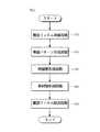
本発明の一実施例によるディスプレイ用透明電極フィルムの製造方法は、図1のように、離型フィルム準備段階(S10)、電極パターン形成段階(S20)、絶縁層形成段階(S30)、基材層形成段階(S40)および離型フィルム除去段階(S50)を含んでなる。 As shown in FIG. 1, a method for manufacturing a transparent electrode film for a display according to an embodiment of the present invention includes a release film preparation step (S10), an electrode pattern formation step (S20), an insulating layer formation step (S30), and a substrate. A layer forming step (S40) and a release film removing step (S50) are included.
離型フィルム準備段階(S10)
離型フィルム準備段階(S10)は、耐熱性フィルム上に離型剤が塗布された離型フィルムを準備し、微細電極パターンが形成される離型フィルムを設ける段階である。Release film preparation stage (S10)
The release film preparation step (S10) is a step of preparing a release film in which a release agent is applied on a heat resistant film and providing a release film on which a fine electrode pattern is formed.
前記離型フィルムは、離型力を調節した離型コートフィルムを使用することができ、ここで離型コートフィルムは、耐熱性フィルム上に離型剤を塗布して製造することができる。 As the release film, a release coat film in which the release force is adjusted can be used, and the release coat film can be manufactured by applying a release agent on a heat resistant film.
前記耐熱性フィルムとしては、ポリエチレンナフタレート(Polyethylene Naphthalate、PEN)、ポリエチレンテレフタレート(polyethylene terephthalate、PET)、ポリエチレン(Polyethylene、PE)、ポリイミド(Polyimide、PI)、ポリカーボネート(Polycarbonate、PC)を使用することができ、これに特に限定されるものではなく、該当分野で知られた様々な材質の耐熱性フィルムを使用することもできる。 As the heat-resistant film, polyethylene naphthalate (PEN), polyethylene terephthalate (PET), polyethylene (Polyethylene, PE), polyimide (Polyimide, PI), polycarbonate (Polycarbonate, PC) is used. However, the present invention is not particularly limited thereto, and heat-resistant films made of various materials known in the corresponding field can also be used.
前記離型剤は、シリコン系またはアクリル系離型剤を使用することが好ましい。 The release agent is preferably a silicon or acrylic release agent.
シリコン系離型剤は、熱圧着工程でも著しい収縮が発生しない耐熱特性を有し、離型力を容易に調節できる長所があるため、より効果的であり、シリコン系離型剤が好ましい。 Silicone release agents are more effective because they have heat-resistant properties that do not cause significant shrinkage even in the thermocompression bonding process, and can easily adjust the release force. Silicone release agents are preferred.
離型剤も該当分野で知られた様々な種類の離型剤を使用することができ、場合によって、これを組み合わせて使用することもできる。 As the release agent, various types of release agents known in the corresponding field can be used, and in some cases, they can be used in combination.
前記離型剤を耐熱性フィルム上に塗布する方法としては、マイクログラビアコーティング法、グラビアコーティング法、スロットダイコーティング法、リバースキスまたはロータリースクリーンコーティング法を使用することができるが、これに限定されるものではない。 As a method for applying the release agent on the heat-resistant film, a micro gravure coating method, a gravure coating method, a slot die coating method, a reverse kiss or a rotary screen coating method can be used, but is not limited thereto. It is not a thing.
電極パターン形成段階(S20)
電極パターン形成段階(S20)は、離型フィルム上に導電性インク組成物を用いて微細電極パターンを形成する段階である。Electrode pattern forming step (S20)
The electrode pattern forming step (S20) is a step of forming a fine electrode pattern on the release film using the conductive ink composition.
前記離型フィルムの離型剤が塗布された方向の表面上に導電性インク組成物を印刷する。 A conductive ink composition is printed on the surface of the release film in the direction in which the release agent is applied.
導電性インク組成物は、金属錯体化合物、金属前駆体、球状金属粒子、金属フレークまたは金属ナノ粒子を使用することが好ましく、導電性物質の材料に応じて2種以上を混合して使用することができる。 The conductive ink composition preferably uses a metal complex compound, a metal precursor, spherical metal particles, metal flakes, or metal nanoparticles, and a mixture of two or more depending on the material of the conductive substance is used. Can do.
より好ましくは、金属錯体化合物または金属前駆体を使用することができる。また、金属錯体化合物または金属前駆体を還元させ、ナノ大きさの金属粒子を製造して混合物としても使用することができる。これを使用すると、従来の技術では形成できなかったナノ大きさの微細電極パターンを容易に形成することができる。 More preferably, a metal complex compound or a metal precursor can be used. Alternatively, the metal complex compound or metal precursor can be reduced to produce nano-sized metal particles that can be used as a mixture. When this is used, a nano-sized fine electrode pattern that cannot be formed by the conventional technique can be easily formed.
本発明に使用される金属前駆体は、一般式MnXで表すことができ、ここでMはAg、Au、Cu、Ni、Co、Pd、Ti、V、Mn、Fe、Cr、Zr、Nb、Mo、W、Ru、Cd、Ta、Re、Os、Ir、Al、Ga、Ge、In、Sn、Sb、Pb、Biであり、nは1〜10の整数であり、Xは酸素、硫黄、ハロゲン、シアノ、シアネート、カーボネート、ニトラート(Nitrate)、サルフェート、ホスフェート、チオシアネート、クロレート、パークロレート、テトラフルオロボレート、アセチルアセトネート、メルカプト、アミド、アルコキシド、カルボキシレートなどを示す。具体的には、たとえば、酢酸(Acetic Acid)金、シュウ酸パラジウム、2−エチルヘキサン酸銀、2−エチルヘキサン酸銅、ステアリン酸鉄、ギ酸(formic acid)ニッケル、亜鉛シトラート(zinc citrate)のようなカルボン酸金属、硝酸銀、シアン化銅、炭酸コバルト、塩化白金、塩化金酸、テトラブトキシチタニウム、ジメトキシジルコニウムジクロライド、アルミニウムイソプロポキシド、バナジウムオキサイド、タンタル(tantalum)メトキシド、ビスマスアセテート、ドデシルメルカプト化金、インジウムアセチルアセトネートのような金属化合物などを一種類以上選択して使用可能である。The metal precursor used in the present invention can be represented by the general formula Mn X, where M is Ag, Au, Cu, Ni, Co, Pd, Ti, V, Mn, Fe, Cr, Zr, Nb, Mo, W, Ru, Cd, Ta, Re, Os, Ir, Al, Ga, Ge, In, Sn, Sb, Pb, Bi, n is an integer of 1 to 10, X is oxygen, Sulfur, halogen, cyano, cyanate, carbonate, nitrate, sulfate, phosphate, thiocyanate, chlorate, perchlorate, tetrafluoroborate, acetylacetonate, mercapto, amide, alkoxide, carboxylate and the like are shown. Specifically, for example, acetic acid (gold), palladium oxalate, silver 2-ethylhexanoate, copper 2-ethylhexanoate, iron stearate, nickel formate (formic acid), zinc citrate (zinc citrate) Carboxylic acid metal such as silver nitrate, copper cyanide, cobalt carbonate, platinum chloride, chloroauric acid, tetrabutoxy titanium, dimethoxyzirconium dichloride, aluminum isopropoxide, vanadium oxide, tantalum methoxide, bismuth acetate, dodecyl mercapto One or more kinds of metal compounds such as gold and indium acetylacetonate can be selected and used.
一般的な金属ナノ粒子の製造方法には、物理的に金属の塊を粉砕して製造する物理的な方法と化学的な方法によって製造する方法がある。 As a general method for producing metal nanoparticles, there are a physical method and a chemical method in which a metal lump is physically pulverized and produced.
化学的な方法をより具体的に説明すると、高圧のガスを噴射して粉末に製造するエアロゾル(aerosol)法、金属化合物と気体還元剤を使用して熱分解により粉末を製造する熱分解法、蒸発原料を加熱蒸発させて粉末を製造する蒸発凝縮法、ゾルゲル法、水熱合成法、超音波合成法、マイクロエマルジョン法、液状還元法などがある。 More specifically, the chemical method is an aerosol method in which high pressure gas is injected to produce powder, a thermal decomposition method in which powder is produced by thermal decomposition using a metal compound and a gas reducing agent, There are an evaporation condensation method, a sol-gel method, a hydrothermal synthesis method, an ultrasonic synthesis method, a microemulsion method, a liquid reduction method and the like in which a raw material is evaporated by heating to evaporate.
ナノ粒子の形成の制御が容易であり、最も経済性が良いと評価されている、分散剤と還元剤を用いて製造する液状還元法が最も多く使用されているが、本発明においては、ナノ粒子を形成できるのならば、すべての方法を使用することができる。 The liquid reduction method using a dispersant and a reducing agent, which is evaluated to be easy to control the formation of nanoparticles and evaluated to be the most economical, is most often used. Any method can be used provided it can form particles.
液状還元法によるナノ粒子の製造方法についての具体的な説明は、本出願人が出願した大韓民国特許出願第2006−0074246号に記載されており、前記特許出願に記載された金属ナノ粒子は、粒子の大きさが均一で、凝集性が最小化されるという長所があり、前記金属ナノ粒子を含有する導電性インクは、150℃以下の低い温度で、短い時間で焼成しても高い導電度を有する、均一で緻密な薄膜または微細パターン形成が容易であるという長所がある。 A specific description of a method for producing nanoparticles by a liquid reduction method is described in Korean Patent Application No. 2006-0074246 filed by the present applicant, and the metal nanoparticles described in the patent application are particles. The conductive ink containing the metal nanoparticles has a high conductivity even when baked in a short time at a low temperature of 150 ° C. or less. It has the advantage that it is easy to form a uniform and dense thin film or fine pattern.
金属導電性物質以外に、必要に応じて、溶媒、安定剤、分散剤、バインダー樹脂(binder resin)、離型剤、還元剤、界面活性剤(surfactant)、湿潤剤(wetting agent)、チキソトロープ剤(thixotropic agent)またはレベリング(levelling)剤、増粘剤のような添加剤などを含ませることができる。 In addition to the metal conductive material, a solvent, a stabilizer, a dispersant, a binder resin, a mold release agent, a reducing agent, a surfactant, a wetting agent, a thixotropic agent as necessary. Additives such as (thixotropic agents) or leveling agents, thickeners, and the like can be included.
前記バインダー樹脂は、様々な基材との付着力が優れたものが好ましい。これに使用可能な物質は、有機高分子物質として、ポリプロピレン、ポリカーボネート、ポリアクリレート、ポリメチルメタアクリレート、セルロースアセテート、ポリ塩化ビニル(polyvinyl chloride)、ポリウレタン、ポリエステル、アルキド樹脂、エポキシ樹脂、フェノキシ樹脂(phenoxy resin)、メラミン樹脂、フェノール樹脂、フェノール変成アルキド樹脂、エポキシ変成アルキド樹脂、ビニル変成アルキド樹脂、シリコン変成アルキド樹脂、アクリルメラミン樹脂、ポリイソシアネート樹脂、エポキシエステル樹脂などを例に挙げることができ、本発明に合えば、これに限定されない。 The binder resin is preferably one having excellent adhesion to various substrates. Materials that can be used for this are organic polymer materials such as polypropylene, polycarbonate, polyacrylate, polymethyl methacrylate, cellulose acetate, polyvinyl chloride, polyurethane, polyester, alkyd resin, epoxy resin, phenoxy resin ( phenoxy resin), melamine resin, phenol resin, phenol modified alkyd resin, epoxy modified alkyd resin, vinyl modified alkyd resin, silicon modified alkyd resin, acrylic melamine resin, polyisocyanate resin, epoxy ester resin, and the like. If it suits the present invention, it will not be limited to this.
また、均一な薄膜に形成するために溶媒が必要な場合があるが、この際、使用可能な溶媒としては、エタノール、イソプロパノール、ブタノールのようなアルコール類、エチレングリコール、グリセリンのようなグリコール類、エチルアセテート、ブチルアセテート、メトキシプロピルアセテート、カルビトールアセテート、エチルカルビトールアセテートのようなアセテート類、メチルセロソルブ、ブチルセロソルブ、ジエチルエーテル、テトラヒドロフラン、ジオキサンのようなエーテル類、メチルエチルケトン、アセトン、ジメチルホルムアミド、1−メチル−2−ピロリドンのようなケトン類、ヘキサン、ヘプタン、ドデカン、パラフィンオイル、ミネラルスピリットのような炭化水素系、ベンゼン、トルエン、キシレンのような芳香族類 、そして、クロロホルムやメチレンクロライド、カーボンテトラクロライドのようなハロゲン置換溶媒、アセトニトリル、ジメチルスルホキシドまたはこれらの混合溶媒などを使用することができる。しかし、溶媒の種類がこれに限定されるものではない。 In addition, in order to form a uniform thin film, a solvent may be required. In this case, usable solvents include alcohols such as ethanol, isopropanol and butanol, glycols such as ethylene glycol and glycerin, Ethyl acetate, butyl acetate, methoxypropyl acetate, carbitol acetate, acetates such as ethyl carbitol acetate, methyl cellosolve, butyl cellosolve, diethyl ether, tetrahydrofuran, ethers such as dioxane, methyl ethyl ketone, acetone, dimethylformamide, 1- Ketones such as methyl-2-pyrrolidone, hydrocarbons such as hexane, heptane, dodecane, paraffin oil, mineral spirits, and aromatics such as benzene, toluene and xylene. Family such, and may be chloroform, methylene chloride, halogen-substituted solvents such as carbon tetrachloride, acetonitrile, dimethyl sulfoxide or a mixed solvent used. However, the kind of solvent is not limited to this.
導電性インク組成物の印刷方法は、グラビアプリンティング法、フレキソプリンティング法、オフセットプリンティング法、リバースオフセットプリンティング法、ディスペンシング法 、スクリーンプリンティング法、ロータリースクリーンプリンティング法またはインクジェットプリンティング法で、前記離型剤の表面上に印刷することが好ましい。この際、コーティング回数は、1回またはそれ以上充填回数を繰り返して使用することもできる。 The printing method of the conductive ink composition is a gravure printing method, a flexo printing method, an offset printing method, a reverse offset printing method, a dispensing method, a screen printing method, a rotary screen printing method, or an ink jet printing method. It is preferable to print on the surface. At this time, the number of times of coating can be used once or more times.
導電性インク組成物の金属含量、溶媒の含量および揮発温度、粘度、チキソトロープ性に応じて、印刷特性の差が発生するため、これは、各方法に適合するように導電性インクの成分を調節して、組成物のレオロジーを充填方法に最適化することが必要である。 Depending on the metal content, solvent content and volatilization temperature, viscosity, and thixotropy of the conductive ink composition, printing characteristics will vary, so this adjusts the components of the conductive ink to suit each method Thus, it is necessary to optimize the rheology of the composition to the filling method.
絶縁層形成段階(S30)
絶縁層形成段階(S30)は、前記電極パターン形成段階(S20)で電極パターンが形成された離型フィルム上に絶縁層を形成する段階である。Insulating layer formation step (S30)
The insulating layer forming step (S30) is a step of forming an insulating layer on the release film on which the electrode pattern is formed in the electrode pattern forming step (S20).
前記絶縁層を形成する物質は、熱または紫外線硬化性樹脂を含む組成物であることが好ましく、熱硬化性樹脂と紫外線硬化性樹脂とを混合して使用することができる。 The substance forming the insulating layer is preferably a composition containing heat or an ultraviolet curable resin, and a mixture of a thermosetting resin and an ultraviolet curable resin can be used.
様々な架橋反応が可能であれば、樹脂組成には制限がないが、耐熱性と光透過率が優れた特性を有することが好ましい。 As long as various crosslinking reactions are possible, the resin composition is not limited, but it is preferable that the resin composition has excellent heat resistance and light transmittance.
前記絶縁層を形成する方法としては、公知の方法が使用することができ、S−ナイフ(S−knife)コーティング法、グラビアコーティング法、フレキソコーティング法、スクリーンコーティング法、ロータリースクリーンコーティング法、スロットダイまたはマイクログラビアコーティング法が好ましいが、これに限定されるものではない。 As the method for forming the insulating layer, known methods can be used, such as S-knife coating method, gravure coating method, flexo coating method, screen coating method, rotary screen coating method, slot die. Alternatively, a microgravure coating method is preferable, but not limited thereto.
微細電極パターンの間の絶縁層の高さは、微細電極パターンの高さと同一であるか、より高く形成されることが好ましく、微細電極パターンの高さよりも0.1μm以上、より好ましくは1μm以上大きいと効果的である。 The height of the insulating layer between the fine electrode patterns is preferably the same as or higher than that of the fine electrode pattern, and is 0.1 μm or more, more preferably 1 μm or more than the height of the fine electrode pattern. Large is effective.
また、絶縁層は、単一層で形成することもでき、微細電極パターンが形成された離型フィルム上に硬化性樹脂を2回以上塗布して、2以上の絶縁層を形成することもできる。 The insulating layer can also be formed as a single layer, and two or more insulating layers can be formed by applying a curable resin twice or more on a release film on which a fine electrode pattern is formed.
基材層形成段階(S40)
基材層形成段階(S40)は、前記絶縁層形成段階(S30)で形成された絶縁層上に基材を積層して基材層を形成する段階である。Base material layer forming step (S40)
The base material layer forming step (S40) is a step of forming a base material layer by laminating the base material on the insulating layer formed in the insulating layer forming step (S30).
前記基材の種類は、特に限定されるものではない。前記基材は、透明な材質、例えば、プラスチックフィルムやガラスで形成することができる。前記プラスチックフィルムとしては、ポリイミド(PI)、ポリエチレンテレフタレート(PET)、ポリエチレンナフタレート(PEN)、ポリエーテルスルホン(PES)、ナイロン(Nylon)、ポリテトラフルオロエチレン(PTFE)、ポリエーテルエーテルケトン(PEEK)、ポリカーボネート(PC)、またはポリアリレート(PAR)を使用することができる。このように、プラスチックフィルムやガラス基板などを使用することができるが、これに限定されない。 The kind of the base material is not particularly limited. The substrate can be formed of a transparent material such as a plastic film or glass. Examples of the plastic film include polyimide (PI), polyethylene terephthalate (PET), polyethylene naphthalate (PEN), polyethersulfone (PES), nylon (Nylon), polytetrafluoroethylene (PTFE), and polyetheretherketone (PEEK). ), Polycarbonate (PC), or polyarylate (PAR). Thus, a plastic film, a glass substrate, or the like can be used, but is not limited thereto.
前記基材を絶縁層上に形成する方法としては、熱圧着または接着剤による接着方法を使用することができる。 As a method of forming the base material on the insulating layer, a thermocompression bonding method or an adhesion method using an adhesive can be used.
熱圧着時には、前記絶縁層上に前記基材を積層した後に100〜300℃、好ましくは120〜200℃、より好ましくは140〜175℃の温度条件で圧着して貼付することができる。 At the time of thermocompression bonding, after laminating the base material on the insulating layer, the base material can be bonded by pressure bonding at a temperature of 100 to 300 ° C, preferably 120 to 200 ° C, more preferably 140 to 175 ° C.
場合によっては、前記絶縁層がB−ステージの半硬化状態で前記基材を貼付して使用することもできる。 In some cases, the insulating layer can be used by attaching the base material in a B-stage semi-cured state.
微細電極パターンが印刷された以後に、基材を熱圧着して基材層を貼付するため、基材層上に電極パターンを形成する場合より、付着が容易で付着力が優れて、透明電極フィルムとしての耐久性が向上する。 After the fine electrode pattern is printed, the base material layer is pasted by thermocompression bonding. Therefore, it is easier to attach and has better adhesion than the case where the electrode pattern is formed on the base material layer. Durability as a film is improved.
離型フィルム除去段階(S50)
離型フィルム除去段階(S50)は、離型フィルムを除去して、最終の透明電極フィルムを製造する段階である。Release film removal step (S50)
The release film removing step (S50) is a step of removing the release film and manufacturing the final transparent electrode film.
離型フィルムを除去して、最終の透明電極フィルムが製造されるが、透明電極フィルムの信頼性を向上させるために、図2に示すように、残余導電性インク組成物処理段階(S60)または導電性物質形成段階(S70)をさらに含むこともできる。 The release film is removed to produce the final transparent electrode film. In order to improve the reliability of the transparent electrode film, as shown in FIG. 2, the residual conductive ink composition treatment step (S60) or A conductive material forming step (S70) may be further included.
離型フィルムを除去した後、離型フィルムが含まれた絶縁層上に導電性インク組成物の残余物が残っていなければ、導電性インク組成物の処理なしですぐ導電性物質形成段階を実施するか、残余導電性インク組成物処理段階を経てすぐ透明電極フィルムとして使用が可能である。 After removing the release film, if there is no residue of the conductive ink composition on the insulating layer containing the release film, the conductive material forming step is performed immediately without treatment of the conductive ink composition. Alternatively, it can be used as a transparent electrode film immediately after the residual conductive ink composition treatment step.
のみならず、導電性インク組成物処理段階と導電性物質形成段階の両方を順次に適用することもできる。 In addition, both the conductive ink composition treatment step and the conductive material formation step can be applied sequentially.
残余導電性インク組成物処理段階(S60)
残余導電性インク組成物処理段階(S60)は、微細電極パターン領域の間に残っている導電性インク組成物を除去する段階であって、残余導電性インク組成物を除去することにより、透明電極フィルムとしての透過率を向上させることができる。Residual conductive ink composition processing step (S60)
The residual conductive ink composition processing step (S60) is a step of removing the conductive ink composition remaining between the fine electrode pattern regions, and the transparent conductive electrode composition is removed by removing the residual conductive ink composition. The transmittance as a film can be improved.
電極パターン形成段階(S20)で離型剤の表面上に導電性インク組成物を用いて微細電極パターンを印刷すると、微細電極パターンが形成される位置ではない領域に導電性インク組成物が残留する場合がある。 When the fine electrode pattern is printed on the surface of the release agent using the conductive ink composition in the electrode pattern formation step (S20), the conductive ink composition remains in a region where the fine electrode pattern is not formed. There is a case.
離型フィルムを除去したら、残余導電性インク組成物は、絶縁層上に存在するようになって、残余導電性インク組成物に含まれた微細金属組成物は、透明電極フィルムの透過率を低下させ、また、耐電圧特性に問題を引き起こすことになるため、残余導電性インク組成物を除去することにより、透明電極の特性を著しく向上させることができる。 When the release film is removed, the residual conductive ink composition is present on the insulating layer, and the fine metal composition contained in the residual conductive ink composition reduces the transmittance of the transparent electrode film. In addition, since a problem is caused in the withstand voltage characteristics, the characteristics of the transparent electrode can be remarkably improved by removing the residual conductive ink composition.
絶縁層表面の微細電極パターンの間に残っている導電性インク組成物を溶解させるために、エッチング液を基材表面に塗布することができ、エッチング液の塗布方法は、通常のコーティング法によって行うことができる。 In order to dissolve the conductive ink composition remaining between the fine electrode patterns on the surface of the insulating layer, an etching solution can be applied to the substrate surface, and the etching solution is applied by a normal coating method. be able to.
エッチング液は、アンモニウムカルバメート系、アンモニウムカーボネート系、アンモニウムバイカーボネート系、カルボン酸系、ラクトン系、ラクタム系、環状酸無水物系化合物、酸−塩基塩複合体、酸−塩基−アルコール系複合体またはメルカプト(mercapto)系化合物のうちの少なくとも1つおよび酸化剤を含むことが好ましい。 Etching solution is ammonium carbamate, ammonium carbonate, ammonium bicarbonate, carboxylic acid, lactone, lactam, cyclic acid anhydride compound, acid-base salt complex, acid-base-alcohol complex or It preferably contains at least one mercapto compound and an oxidizing agent.
例えば、酸化剤と1つ以上の前記の化合物およびこれらの混合物を常圧または加圧状態で溶媒なしで直接反応させるか、溶媒を使用する場合は、水、メタノール、プロパノール、イソプロパノール、ブタノール、エタノールアミンのようなアルコール類、エチレングリコール、グリセリンのようなグリコール類、エチルアセテート、ブチルアセテート、カルビトールアセテートのようなアセテート類、ジエチルエーテル、テトラヒドロフラン、ジオキサンのようなエーテル類、メチルエチルケトン、アセトンのようなケトン類、ヘキサン、ヘプタンのような炭化水素系、ベンゼン、トルエンのような芳香族、そしてクロロホルムやメチレンクロライド、カーボンテトラクロライドのようなハロゲン置換溶媒、パーフルオロカーボンのようなフッ素系溶媒またはこれらの混合溶媒などを使用することができる。圧力容器のような加圧状態では、低沸点のフッ素系溶剤や液化炭酸ガスなども使用可能である。本発明のエッチング液の製造方法を特に制限する必要はない。すなわち、本発明の目的に合えば、公知のいかなる方法を使用してもよい。 For example, when an oxidant and one or more of the above-mentioned compounds and mixtures thereof are reacted directly at normal pressure or under pressure without a solvent, or when a solvent is used, water, methanol, propanol, isopropanol, butanol, ethanol Alcohols such as amines, glycols such as ethylene glycol and glycerine, acetates such as ethyl acetate, butyl acetate and carbitol acetate, ethers such as diethyl ether, tetrahydrofuran and dioxane, methyl ethyl ketone and acetone Ketones, hydrocarbons such as hexane and heptane, aromatics such as benzene and toluene, halogen-substituted solvents such as chloroform, methylene chloride and carbon tetrachloride, and fluorocarbons such as perfluorocarbon And the like can be used Motokei solvent or solvent mixtures thereof. In a pressurized state such as a pressure vessel, a low boiling point fluorine-based solvent, liquefied carbon dioxide gas, or the like can be used. There is no particular restriction on the method for producing the etching solution of the present invention. That is, any known method may be used as long as the object of the present invention is met.
前記エッチング液において、 前記酸化剤は、例えば、酸素、オゾンなどのような酸化性気体、過酸化水素、Na2O2、KO2、NaBO3、(NH4)S2O8、H2SO5、(CH3)3CO2H、(C6H5CO2)2などのような過酸化物、HCO3H、CH3CO3H、CF3CO3H、C6H5CO3H、m−ClC6H5−CO3Hなどのような過酸素酸、硝酸、硫酸、ヨード(I2)、Fe(NO3)3、Fe2(SO4)3、K3Fe(CN)6、(NH4)2Fe(SO4)2、Ce(NH4)4(SO4)4、NaIO4、KMnO4、K2CrO4などのように、一般的によく知られている酸化性無機酸または金属、非金属化合物などがここに含まれる。このような酸化剤を使用するときには、単独または最小限1つ以上の酸化剤を混合して使用してもよい。In the etching solution, the oxidizing agent may be, for example, an oxidizing gas such as oxygen or ozone, hydrogen peroxide, Na2 O2 , KO2 , NaBO3 , (NH4 ) S2 O8 , or H2 SO.5 , peroxides such as (CH3 )3 CO2 H, (C6 H5 CO2 )2 , HCO3 H, CH3 CO3 H, CF3 CO3 H, C6 H5 CO3 Peroxyacids such as H, m-Cl6 H5 —CO3 H, nitric acid, sulfuric acid, iodine (I2 ), Fe (NO3 )3 , Fe2 (SO4 )3 , K3 Fe (CN )6 , (NH4 )2 Fe (SO4 )2 , Ce (NH4 )4 (SO4 )4 , NaIO4 , KMnO4 , K2 CrO4, etc. Oxidizing inorganic acids or metals, non-metallic compounds, etc. are included here That. When such an oxidizing agent is used, it may be used alone or as a mixture of at least one oxidizing agent.
前記エッチング液は、絶縁層の表面に残っている導電性インクを効果的に溶解するために、エッチング液組成物に親水特性を付与することが好ましいことがある。アンモニウムカルバメート系、アンモニウムカーボネート系、アンモニウムバイカーボネート系、カルボン酸系、ラクトン系、ラクタム系、環状酸無水物系、酸−塩基塩複合体、酸−塩基−アルコール系複合体、メルカプト系化合物の炭素数を調節して、親水特性の程度を調節することが好ましい。 In order to effectively dissolve the conductive ink remaining on the surface of the insulating layer, the etching solution may preferably impart hydrophilic properties to the etching solution composition. Carbon of ammonium carbamate, ammonium carbonate, ammonium bicarbonate, carboxylic acid, lactone, lactam, cyclic acid anhydride, acid-base salt complex, acid-base-alcohol complex, mercapto compound Preferably, the number is adjusted to adjust the degree of hydrophilic properties.
ここで、アンモニウムカルバメート系化合物、アンモニウムカーボネート系化合物およびアンモニウムバイカーボネート系化合物は、本出願人の韓国登録第0727466号に具体的に説明されており、カルボン酸系の化合物としては、安息香酸、オレイン酸、プロピオン酸、マロン酸、ヘキサン酸、オクタン酸、デカン酸、ネオデカン酸、シュウ酸、クエン酸、サリチル酸、ステアリン酸、アクリル酸、コハク酸、アジピン酸、グリコール酸、イソブチル酸、アスコルビン酸などを使用することができる。 Here, the ammonium carbamate compound, the ammonium carbonate compound and the ammonium bicarbonate compound are specifically described in the applicant's Korean registration No. 0727466, and carboxylic acid compounds include benzoic acid and olein. Acid, propionic acid, malonic acid, hexanoic acid, octanoic acid, decanoic acid, neodecanoic acid, oxalic acid, citric acid, salicylic acid, stearic acid, acrylic acid, succinic acid, adipic acid, glycolic acid, isobutyric acid, ascorbic acid, etc. Can be used.
ラクトン系化合物としては、β−プロピオラクトン、γ−プロピオラクトン、γ−ブチロラクトン、γ−チオブチロラクトン、α−メチル−γ−ブチロラクトン、β−メチル−γ−ブチロラクトン、γ−バレロラクトン、γ−カプロラクトン、γ−オクタノイックラクトン、δ−バレロラクトン、1、6−ジオキサスピロ[4、4]ノナン−2、7−ジオン、α−メチレン−γ−ブチロラクトン、γ−メチレン−γ−ブチロラクトン、ε−カプロラクトン、ラクチド、グリコライド、テトロン酸、2(5H)−フラノン、β−ヒドロキシ−γ−ブチロラクトン、メバロニックラクトン(mevalonic lactone)、5、6−ジヒドロ−2H−ピラン−2−オン、δ−バレロラクトン、ε−カプロラクトン、γ−カプロラクトン、γ−オクタノイックラクトン(Octanoic lactone)などを使用することができる。 Examples of lactone compounds include β-propiolactone, γ-propiolactone, γ-butyrolactone, γ-thiobutyrolactone, α-methyl-γ-butyrolactone, β-methyl-γ-butyrolactone, γ-valerolactone, γ- Caprolactone, γ-octanoic lactone, δ-valerolactone, 1,6-dioxaspiro [4,4] nonane-2,7-dione, α-methylene-γ-butyrolactone, γ-methylene-γ-butyrolactone, ε- Caprolactone, lactide, glycolide, tetronic acid, 2 (5H) -furanone, β-hydroxy-γ-butyrolactone, mevalonic lactone, 5,6-dihydro-2H-pyran-2-one, δ- Valerolactone, ε-caprolactone, γ-caprolactone, γ-octanoic Or the like can be used lactone (Octanoic lactone).
ラクタム系化合物としては、2−アゼチジノン、2−ピロリジノン、5−メトキシ−2−ピロリジノン、5−メチル−2−ピロリジノン、N−メチルカプロラクタム、2−アザシクロノナノンは、N−アセチルカプロラクタムなどを使用することができる。 As lactam compounds, 2-azetidinone, 2-pyrrolidinone, 5-methoxy-2-pyrrolidinone, 5-methyl-2-pyrrolidinone, N-methylcaprolactam, 2-azacyclononanone use N-acetylcaprolactam, etc. can do.
環状酸無水物としては、無水イタコン酸、無水コハク酸、無水マイレン酸、グルタル酸無水物、オクタデシルコハク酸無水物、2、2−ジメチルコハク酸無水物、2−ドデセン−1−イルコハク酸無水物、ヘキサフルオログルタル酸無水物、3、3−ジメチルグルタル酸無水物、3−エチル−3−メチルグルタル酸無水物、3、5−ジアセチルテトラヒドロピラン−2、4、6−トリオン、ジグリコール酸無水物などを使用することができる。 Examples of cyclic acid anhydrides include itaconic anhydride, succinic anhydride, maleic anhydride, glutaric anhydride, octadecyl succinic anhydride, 2,2-dimethyl succinic anhydride, and 2-dodecen-1-yl succinic anhydride. , Hexafluoroglutaric anhydride, 3,3-dimethylglutaric anhydride, 3-ethyl-3-methylglutaric anhydride, 3,5-diacetyltetrahydropyran-2, 4,6-trione, diglycolic anhydride Things can be used.
メルカプト系の化合物としては、1−メタンチオール、1−エタンチオール、2−ブタンチオール、1−ヘプタンチオール、1−オクタンチオール、1−デカンチオール、1−ヘキサデカンチオール、チオ酢酸、6−メルカプトヘキサン酸、チオ安息香酸、プルプリルメルカプタン、シクロヘキサンチオール、11−メルカプト−1−ウンデカノル、2−メルカプトエタノール、3−メルカプト−1−プロパノール、チオサリチル酸、1−チオグリセロール、2−ナフタレンチオール、メチル3−メルカプトプロピオネート、ガンマメルカプトプロピルトリメトキシシランなどを使用することができる。これに限定されるものではなく、このうち、単一成分で使用してもよく、2種以上の混合物からなるグループの中から選択されたものでもよい。 Mercapto compounds include 1-methanethiol, 1-ethanethiol, 2-butanethiol, 1-heptanethiol, 1-octanethiol, 1-decanethiol, 1-hexadecanethiol, thioacetic acid, 6-mercaptohexanoic acid , Thiobenzoic acid, purpuryl mercaptan, cyclohexanethiol, 11-mercapto-1-undecanol, 2-mercaptoethanol, 3-mercapto-1-propanol, thiosalicylic acid, 1-thioglycerol, 2-naphthalenethiol, methyl 3-mercapto Propionate, gamma mercaptopropyltrimethoxysilane, and the like can be used. It is not limited to this, Among these, it may be used by a single component and may be selected from the group which consists of 2 or more types of mixtures.
前記エッチング組成物のエッチング速度は、コーティングのとき、エッチング液の沈積時間を調節したり、エッチング液の酸化剤またはアンモニウムカルバメート系、アンモニウムカーボネート系、アンモニウムバイカーボネート系、カルボン酸系、ラクトン系、ラクタム系、環状酸無水物系、酸−塩基塩複合体、酸−塩基−アルコール系複合体、メルカプト系化合物の濃度を調節して制御することが好ましく、必要に応じて、エッチング過程を繰り返して使用することができる。また、無機酸や塩基を含むエッチング液の場合、別途の水や有機溶剤で洗浄して除去することができる。 The etching rate of the etching composition can be adjusted by adjusting the deposition time of the etchant during coating, or by oxidizing agent of the etchant or ammonium carbamate, ammonium carbonate, ammonium bicarbonate, carboxylic acid, lactone, lactam. System, cyclic acid anhydride, acid-base salt complex, acid-base-alcohol complex, and mercapto compound are preferably adjusted and controlled. Repeated etching process is used as necessary. can do. In the case of an etching solution containing an inorganic acid or base, it can be removed by washing with separate water or an organic solvent.
エッチング液によって溶解した残余導電性インク組成物を物理的な力で押し出して除去することができる。 The residual conductive ink composition dissolved by the etching solution can be removed by being pushed out by a physical force.
溶解した残余導電性インク組成物を押し出す方法または押し出す処理部材の制限はないが、ドクターブレード(doctor blade)、ワイパー(wiper)またはブラシ(brush)を用いることができる。より好ましくは、ブラシを用いる。ブラシは、物理的な力を減少させることによって、基材表面のきず、インク流失を効果的に防止することができる。 Although there is no limitation on the method of extruding the dissolved residual conductive ink composition or the processing member to be extruded, a doctor blade, a wiper or a brush can be used. More preferably, a brush is used. The brush can effectively prevent scratches on the substrate surface and ink loss by reducing physical force.
これは、1回以上行われることができ、様々な方法、特にドクターブレード、ワイパー、ブラシを混用して使用することもできる。 This can be done one or more times, and various methods can be used, especially doctor blades, wipers and brushes.
残余物処理部材を用いて溶解した残余導電性インク組成物を押し出し、絶縁層上の微細電極パターンの間の表面に残っている導電性インク組成物の成分である金属物質または有機物質などを除去することができる。 The residual conductive ink composition dissolved by using the residual material processing member is extruded to remove the metal material or organic material that is a component of the conductive ink composition remaining on the surface between the fine electrode patterns on the insulating layer. can do.
この他にも、溶解した残余導電性インク組成物を押し出すための方法として、別途の振動または揺動、エアーを用いることもできる。 In addition to this, as a method for extruding the dissolved residual conductive ink composition, separate vibration, oscillation, or air can be used.
導電性物質形成段階(S70)
導電性物質形成段階(S70)は、離型フィルムが除去された微細電極パターン上に導電性物質を蒸着するか、プリンティングして、ハイブリッド型透明電極フィルムを製造する段階である。Conductive substance formation stage (S70)
The conductive material forming step (S70) is a step of manufacturing a hybrid transparent electrode film by depositing or printing a conductive material on the fine electrode pattern from which the release film has been removed.
本段階は、素子の内部電極に対して使用され、必要に応じて追加することができる。 This stage is used for the internal electrodes of the device and can be added as needed.
また、導電性物質形成段階(S70)は、離型フィルムが除去されてから(S50)、すぐ実施することもでき、残余導電性インク組成物を除去する残余導電性インク組成物処理段階(S60)後に実施することもできる。残余導電性インク組成物を除去した後に、微細電極パターン上に導電性物質を形成すると、信頼性の高い透明電極フィルムの具現が可能である。 Further, the conductive material forming step (S70) can be performed immediately after the release film is removed (S50), and the residual conductive ink composition treatment step (S60) for removing the residual conductive ink composition. ) Can be implemented later. When a conductive material is formed on the fine electrode pattern after removing the remaining conductive ink composition, a highly reliable transparent electrode film can be realized.
微細電極パターン上に形成することができる導電性物質は、ITO、AZO、CNT、グラフェンまたは導電性高分子であることが好ましく、導電性高分子は、PEDOT[ポリ(3、4−エチレンジオキシチオフェノン)(Poly(3、4−Ethylene dioxythiophene))]またはPSS:PEDOT[ポリ(3、4−エチレンジオキシチオフェノン)(Poly(3、4−Ethylene dioxythiophene)):ポリ(4−スチレンスルホネート)(Poly(4−Styrene sulfonate))]を使用することができる。 The conductive material that can be formed on the fine electrode pattern is preferably ITO, AZO, CNT, graphene, or a conductive polymer. The conductive polymer is PEDOT [poly (3,4-ethylenedioxy Thiophenone) (Poly (3,4-Ethylene dioxythiophene))] or PSS: PEDOT [Poly (3,4-ethylenedioxythiophenone) (Poly (3,4-Ethylene dioxythiophene)): Poly (4-styrenesulfonate) ) (Poly (4-Styrene sulfate))] can be used.
導電性物質は、微細パターン電極の上に蒸着してパターニングするか、直接プリンティングして形成することができ、ITOまたはAZOの材料は、ターゲット形態で真空蒸着(sputtering)するか、インク化して、薄膜コーティング組成物でプリンティングすることが好ましい。 The conductive material may be deposited on the fine pattern electrode and patterned, or directly printed, and the ITO or AZO material may be vacuum deposited (sputtered) in a target form or converted into an ink. Printing with a thin film coating composition is preferred.
このようなハイブリッド形態の透明電極フィルムは、2つの電極間の界面特性に優れ、高い導電度を有することから、高信頼性を要求する分野に使用することができる。 Such a transparent electrode film in a hybrid form is excellent in interface characteristics between two electrodes and has high conductivity, so that it can be used in a field requiring high reliability.
透明電極フィルムの製造のための前記の段階は、ロール・ツー・ロール(roll−to−roll)の連続工程により行うことができ、これによって、生産速度が増加して、生産効率を増大させることができる。 The above steps for the production of the transparent electrode film can be performed by a roll-to-roll continuous process, thereby increasing the production speed and increasing the production efficiency. Can do.
以下では、図3を参照して、本発明について具体的に説明する。
図3a〜図3jは、本発明の一実施例に係る透明電極フィルムの製造方法を順次に図式化した断面図である。Hereinafter, the present invention will be specifically described with reference to FIG.
3a to 3j are cross-sectional views sequentially illustrating a transparent electrode film manufacturing method according to an embodiment of the present invention.
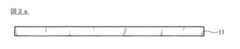
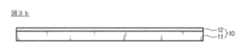
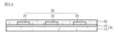
図3aに示すように、耐熱性フィルム11が準備される。耐熱性フィルム11は、PEN、PET、PE、PL、PCのような、様々な材質のフィルムが使用可能である。 As shown in FIG. 3a, a heat
図3bは、耐熱性フィルム11上に離型剤12を塗布して離型フィルム10を製造する。離型フィルム10は、離型力を有するものであれば、いかなる形態でも関係ないが、耐熱性離型力を調節した離型コートフィルムの形態であることが好ましい。 In FIG. 3 b, a
この後、基材層40を熱圧着のような方式で貼付する工程が続くため、離型剤12は、熱圧着工程でも著しい収縮が発生しない耐熱特性を有する物質であることが好ましく、シリコン系離型剤を使用することが効果的である。 Then, since the process of sticking the
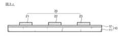
次に、図3cに示すように、離型フィルム10上に微細電極パターン20を形成することになる。 Next, as shown in FIG. 3 c, the
離型フィルム10は、除去される対象であり、離型力が優れた離型剤12面の上に印刷された微細電極パターン20は、メッシュ状に形成することができる。 The
導電性インク組成物としては、金属錯体化合物または金属前駆体を使用することができ、グラビアプリンティング法、フレキソプリンティング法、オフセットプリンティング法、リバースオフセットプリンティング法、ディスペンシング法、スクリーンプリンティング法、ロータリースクリーンプリンティング法またはインクジェットプリンティング法などを使用することができるが、これに限定されない。 As the conductive ink composition, a metal complex compound or a metal precursor can be used. Gravure printing method, flexographic printing method, offset printing method, reverse offset printing method, dispensing method, screen printing method, rotary screen printing A method or an inkjet printing method can be used, but is not limited thereto.
導電性インク組成物の印刷は1回に限定されるものではなく、場合によって、複数回繰り返すことができる。 Printing of the conductive ink composition is not limited to once, and may be repeated a plurality of times depending on the case.
微細電極パターン20は、導電性インク組成物を用いて印刷される。印刷時に微細電極パターン20が形成される位置ではない領域に、導電性インク組成物が残ることがあっても、この後、残余導電性インク組成物50を処理する段階を追加することができる。 The
この後、図3dに示すように、微細電極パターン20が印刷された離型剤12の表面に熱または紫外線硬化性樹脂が塗布されて絶縁層30を形成する。 Thereafter, as shown in FIG. 3d, heat or ultraviolet curable resin is applied to the surface of the
絶縁層30の高さは、該当図面に示すように、微細電極パターン20の高さよりも高く形成されることが効果的であり、微細電極パターンの高さよりも0.1μm以上、より好ましくは1μm以上大きいことが好ましい。 The height of the insulating
絶縁層30が形成された以後、図3eに示すように、絶縁層30上に基材層40を積層する。 After the insulating
基材層40の基材は、種類に限定されず、透明電極フィルムとしてプラスチックフィルムやガラスのような透明な材質を使用することができる。 The base material of the
基材は、100〜300℃の温度で熱圧着して絶縁層30上に基材を貼付することが好ましく、接着剤を絶縁層30上に塗布して基材を接着する方法も使用可能である。 The base material is preferably bonded by thermocompression bonding at a temperature of 100 to 300 ° C. and the base material is pasted on the insulating
接着剤を使用して基材を接着する場合に、前記接着剤は、透明性のある接着剤を使用することが好ましく、ポリビニルアルコール系接着剤、アクリル系接着剤、ビニルアセテート系接着剤、ウレタン系接着剤、ポリエステル系接着剤、ポリオレフィン系接着剤、ポリビニルアルキルエーテル系接着剤を使用することができ、基材の種類に応じて、接着剤を2種以上混合して使用することができる。 When adhering a substrate using an adhesive, the adhesive is preferably a transparent adhesive, such as a polyvinyl alcohol adhesive, an acrylic adhesive, a vinyl acetate adhesive, or urethane. Type adhesives, polyester type adhesives, polyolefin type adhesives, polyvinyl alkyl ether type adhesives can be used, and two or more types of adhesives can be mixed and used depending on the type of substrate.
接着剤層の厚さに特に制限はなく、物性を考慮した通常の厚さに設定することができる。 There is no restriction | limiting in particular in the thickness of an adhesive bond layer, It can set to the normal thickness which considered the physical property.
基材を貼付した後に、離型フィルム10を除去して、透明電極フィルムを製造することができる。これは、図3fに示されている。 After pasting the substrate, the
離型フィルム10の離型剤12の離型力を調節することによって、離型フィルム10を微細電極パターンが形成された絶縁層30から分離する。 The
これによって、図3gに示すように、微細電極パターン20が外部に露出するため、表面粗度が優れたディスプレイ用透明電極フィルムが具現可能である。 Accordingly, as shown in FIG. 3g, since the
透明電極フィルムの信頼性を向上させるため、図3h、3i、3jに示した工程を追加で実施することができる。 In order to improve the reliability of the transparent electrode film, the steps shown in FIGS. 3h, 3i, and 3j can be additionally performed.
図3hは、前記で言及したように、導電性インク組成物を印刷して微細電極パターン20を形成する際、微細電極パターン20が形成されない位置に導電性インク組成物が残ることがあり、離型フィルム10を除去後に、導電性インク組成物が絶縁層30上に依然として残っているため、これを除去する工程を追加で実施することができる。 In FIG. 3h, as mentioned above, when the
残余導電性インク組成物50をエッチング液で溶解して、これを押し出すことによって、微細電極パターンが形成される位置ではない領域から金属物質または有機物質を除去することができる。 By dissolving the residual
残余導電性インク組成物50の残余量に応じて、エッチング液の濃度や沈積速度を制御することが好ましい。 It is preferable to control the concentration and deposition rate of the etching solution according to the remaining amount of the remaining
溶解した残余導電性インク組成物を押し出す方法としては、様々な物理的な力によって押し出すことが挙げられるが、該当図面においては、ドクターブレード70を使用した。これは1回以上実施することができ、様々な種類のスクイズを混用して使用することができる。 Examples of a method for extruding the dissolved residual conductive ink composition include extruding by various physical forces. In the drawings, a
残余導電性インク組成物50を除去することによって、耐電圧特性および光透過率を向上させることができる。 By removing the residual
この後、図3iおよび図3jに示すように、微細電極パターン上に導電性物質を形成することができる。 Thereafter, as shown in FIGS. 3i and 3j, a conductive material can be formed on the fine electrode pattern.
図3iに示すように、ITO、AZO、NT、グラフェン、導電性高分子のような導電性物質を微細電極パターン20が形成された絶縁層30上に直接プリンティングした後に、図3jに示すように、エッチングして、ハイブリッド形態の透明電極フィルムを形成することができる。 As shown in FIG. 3J, after printing a conductive material such as ITO, AZO, NT, graphene, conductive polymer directly on the insulating
これは、必ずしも図3hの工程後に行われるものではなく、離型フィルム10が除去された図3gの透明電極フィルムの状態で導電性物質を形成することもできる。 This is not necessarily performed after the step of FIG. 3h, and the conductive material can be formed in the state of the transparent electrode film of FIG. 3g from which the
本発明の一実施例によるディスプレイ用透明電極フィルムは、離型フィルム上に導電性インク組成物を微細電極パターンに印刷して形成された電極パターンと、前記電極パターンが形成された前記離型フィルム上に絶縁性樹脂を塗布して形成された絶縁層、および前記離型フィルムと接した前記絶縁層の一面の反対面である前記絶縁層の他面上に積層された基材層を含み、前記電極パターンは、前記絶縁層の内部に埋め込まれるように位置し、前記電極パターンの一面は、前記絶縁層の前記一面の表面に露出して、前記離型フィルムと接するように位置し得る。 The transparent electrode film for display according to an embodiment of the present invention includes an electrode pattern formed by printing a conductive ink composition on a release film on a fine electrode pattern, and the release film on which the electrode pattern is formed. An insulating layer formed by applying an insulating resin thereon, and a base material layer laminated on the other surface of the insulating layer that is the opposite surface of the insulating layer in contact with the release film; The electrode pattern may be positioned so as to be embedded in the insulating layer, and one surface of the electrode pattern may be positioned so as to be exposed on the surface of the one surface of the insulating layer and in contact with the release film.
本発明の他の実施例によるディスプレイ用透明電極フィルムは、離型フィルム上に導電性インク組成物を微細電極パターンに印刷して形成された電極パターン、前記微細電極パターンの間の溝が充填されるように絶縁性樹脂を全面に塗布して形成された絶縁層、および前記離型フィルムと接した前記絶縁層の一面の反対面である前記絶縁層の他面上に積層された基材層を含み、前記電極パターンは、前記絶縁層の内部に埋め込まれるように位置し、前記電極パターンの一面は、前記絶縁層の前記一面の表面に露出して、前記離型フィルムと接するように位置し得る。 A transparent electrode film for a display according to another embodiment of the present invention has an electrode pattern formed by printing a conductive ink composition on a release film on a release film, and grooves between the electrode patterns are filled. An insulating layer formed by coating an insulating resin over the entire surface, and a base material layer laminated on the other surface of the insulating layer that is the opposite surface of the insulating layer in contact with the release film The electrode pattern is positioned so as to be embedded in the insulating layer, and one surface of the electrode pattern is exposed on the surface of the one surface of the insulating layer and positioned so as to contact the release film Can do.
本発明のまた他の実施例によるディスプレイ用透明電極フィルムは、離型フィルム上に導電性インク組成物を微細電極パターンに印刷して形成された電極パターン、前記微細電極パターンが形成された前記離型フィルム上に前記微細電極パターンが覆われるように絶縁性樹脂を塗布して形成された絶縁層、および前記離型フィルムと接した前記絶縁層の一面の反対面である前記絶縁層の他面上に積層された基材層を含むディスプレイ用透明電極フィルムであって、前記電極パターンは、前記絶縁層の内部に埋め込まれるように位置し、前記電極パターンの一面は、前記絶縁層の前記一面の表面に露出して、前記離型フィルムと接するように位置しており、前記離型フィルムが除去された前記微細電極パターンの間に残っている残余導電性インク組成物をエッチング液で溶解させ、溶解した前記残余導電性インク組成物を押し出すことによって、残余導電性インク組成物を除去して形成することができる。 According to another embodiment of the present invention, a transparent electrode film for a display includes an electrode pattern formed by printing a conductive ink composition on a release film on a fine electrode pattern, and the release electrode on which the fine electrode pattern is formed. An insulating layer formed by applying an insulating resin so that the fine electrode pattern is covered on the mold film, and the other surface of the insulating layer that is the opposite surface of the insulating layer in contact with the release film A transparent electrode film for a display including a base material layer laminated thereon, wherein the electrode pattern is positioned so as to be embedded in the insulating layer, and one surface of the electrode pattern is the one surface of the insulating layer Residual conductive ins that are exposed on the surface of the substrate and are in contact with the release film and remain between the fine electrode patterns from which the release film has been removed The composition is dissolved in an etching solution, by extruding the residual conductive ink composition dissolved, can be formed by removing the residual conductive ink composition.
本発明のまた他の実施例によるディスプレイ用透明電極フィルムは、離型フィルム上に導電性インク組成物を微細電極パターンに印刷して形成された電極パターン、前記電極パターンが形成された前記離型フィルム上に絶縁性樹脂を塗布して形成された絶縁層、および前記離型フィルムと接した前記絶縁層の一面の反対面である前記絶縁層の他面上に積層された基材層を含むディスプレイ用透明電極フィルムであって、前記電極パターンは、前記絶縁層の内部に埋め込まれるように位置し、前記電極パターンの一面は、前記絶縁層の前記一面の表面に露出して、前記離型フィルムと接するように位置しており、前記離型フィルムが除去された状態で、前記微細電極パターンの間に残っている残余導電性インク組成物をエッチング液で溶解させ、溶解した前記残余導電性インク組成物を押し出すことによって、残余導電性インク組成物を除去した前記微細電極パターン上に形成した導電性物質をさらに含むことができる。 A transparent electrode film for a display according to another embodiment of the present invention includes an electrode pattern formed by printing a conductive ink composition on a release film on a fine electrode pattern, and the mold release having the electrode pattern formed thereon. An insulating layer formed by applying an insulating resin on the film, and a base material layer laminated on the other surface of the insulating layer that is the opposite surface of the insulating layer in contact with the release film A transparent electrode film for a display, wherein the electrode pattern is positioned so as to be embedded in the insulating layer, and one surface of the electrode pattern is exposed on the surface of the one surface of the insulating layer. Residual conductive ink composition remaining between the fine electrode patterns is dissolved with an etching solution in a state where the film is located and the release film is removed. By extruding dissolved the residual conductive ink composition may further include a conductive material formed on the fine electrode pattern to remove residual conductive ink composition.
前記導電性インク組成物、前記絶縁性樹脂、前記エッチング液および前記導電性物質は、ディスプレイ用透明電極フィルムの製造方法で説明したものと同一である。 The conductive ink composition, the insulating resin, the etching solution, and the conductive substance are the same as those described in the method for producing the transparent electrode film for display.
本発明例によるディスプレイ用透明電極フィルムの表面粗度は、0.05〜0.3μmとすることができ、好ましくは0.10〜0.2μmであり、最も好ましくは0.10〜0.15μmである。 The surface roughness of the transparent electrode film for display according to the example of the present invention can be 0.05 to 0.3 μm, preferably 0.10 to 0.2 μm, and most preferably 0.10 to 0.15 μm. It is.
また、本発明によるディスプレイ用透明電極フィルムの面抵抗は、10mΩ/sq〜100kΩ/sqとすることができ、好ましくは10mΩ/sq〜10kΩ/sqであり、より好ましくは3.0〜18.5Ω/sqであり、最も好ましくは3.0〜10.5Ω/sqである。 Further, the sheet resistance of the transparent electrode film for display according to the present invention can be 10 mΩ / sq to 100 kΩ / sq, preferably 10 mΩ / sq to 10 kΩ / sq, more preferably 3.0 to 18.5Ω. / Sq, most preferably 3.0 to 10.5 Ω / sq.
また、本発明によるディスプレイ用透明電極フィルムの透過率は、60〜99%とすることができ、より好ましくは70〜99%であり、最も好ましくは83〜91%である。 Moreover, the transmittance | permeability of the transparent electrode film for a display by this invention can be 60 to 99%, More preferably, it is 70 to 99%, Most preferably, it is 83 to 91%.
以下では、実施例により、本発明について具体的に説明する。本発明の範囲は、実施例に限定されない。 Below, an Example demonstrates this invention concretely. The scope of the present invention is not limited to the examples.
実施例1
離型フィルムとして耐熱シリコン離型コートフィルム(SKC社、SG32)の上に、導電性金属組成物(インクテック、TEC−PA−010)で微細電極パターンをリバースオフセットプリンティング(Narae Nanotech社)で印刷した後、130℃で20分間乾燥して、3μm線幅の電極パターンを形成した。スロットダイコーター(Pactive Korea社)を使用し、電極パターン上に、紫外線硬化型樹脂(Minuta Technology社、MIR−30)コーティング液を、乾燥厚さ70μmでコーティングして絶縁層を形成し、絶縁層上に12μm厚さのPETフィルムを120℃の温度で2分間ホットプレス(hot press)で熱圧着した後、離型コートフィルムを除去して、透明電極フィルムを製造した。下記の表1に、製造された製品の面抵抗、透過率、ヘイズ、イエローインデックス(Yellow Index)、表面粗度の結果を記載し、図4にSEM(Scanning Electron Microscope)イメージを示した。表面粗度は、Nanosystem社の3次元測定器であるNV−1000を用いて、製造された透明電極フィルムについて測定した。Example 1
A fine electrode pattern is printed by reverse offset printing (Narae Nanotech) on a heat-resistant silicone release coating film (SKC, SG32) as a release film with a conductive metal composition (Inktec, TEC-PA-010). Then, it was dried at 130 ° C. for 20 minutes to form an electrode pattern having a 3 μm line width. Using a slot die coater (Pactive Korea), an ultraviolet curable resin (Minuta Technology, MIR-30) coating solution is coated on the electrode pattern with a dry thickness of 70 μm to form an insulating layer. A 12 μm thick PET film was thermocompression bonded at 120 ° C. for 2 minutes with a hot press, and then the release coat film was removed to produce a transparent electrode film. Table 1 below shows the results of surface resistance, transmittance, haze, yellow index, and surface roughness of the manufactured product, and FIG. 4 shows an SEM (Scanning Electron Microscope) image. The surface roughness was measured on the produced transparent electrode film using NV-1000, a three-dimensional measuring device manufactured by Nanosystem.
実施例2
離型フィルムとして耐熱シリコン離型コートフィルム(SKC社、SG32)の上に、導電性インク組成物(インクテック、TEC−IM−20)で微細電極パターンをリバースオフセットプリンティング(Narae Nanotech社)で印刷した後、130℃で20分間乾燥して、3μm線幅の微細電極パターンを形成した。スロットダイコーター(Pactive Korea社)を使用し、電極パターン上に、紫外線硬化型樹脂(Minuta Technology社、MRI−30)コーティング液を、乾燥厚さ70μmでコーティングして絶縁層を形成し、絶縁層上に12μm厚さのPETフィルムを120℃の温度で2分間ホットプレス(hot press)で熱圧着した後、離型フィルムを除去して、透明電極フィルムを製造した。下記の表1に、製造された製品の面抵抗、透過率、ヘイズ、イエローインデックス、表面粗度の結果を記載し、図4にSEMイメージを示した。Example 2
A fine electrode pattern is printed by reverse offset printing (Narae Nanotech) on a heat-resistant silicone release coat film (SKC, SG32) as a release film with a conductive ink composition (Inktec, TEC-IM-20). Then, it was dried at 130 ° C. for 20 minutes to form a fine electrode pattern having a line width of 3 μm. Using a slot die coater (Pactive Korea), an ultraviolet curable resin (Minuta Technology, MRI-30) coating solution is coated on the electrode pattern with a dry thickness of 70 μm to form an insulating layer. A 12 μm-thick PET film was thermocompression bonded at 120 ° C. for 2 minutes with a hot press, and then the release film was removed to produce a transparent electrode film. Table 1 below shows the results of sheet resistance, transmittance, haze, yellow index, and surface roughness of the manufactured product, and FIG. 4 shows an SEM image.
実施例3
離型フィルムとして耐熱シリコン離型コートフィルム(SKC社、SG32)の上に、導電性インク組成物(インクテック、TEC−PA−021)で微細電極パターンをリバースオフセットプリンティング(Narae Nanotech社)で印刷した後、130℃で20分間乾燥して、3μm線幅の電極パターンを形成した。スロットダイコーター(Pactive Korea社)を使用し、電極パターン上に、紫外線硬化型樹脂(Minuta Technology社、MRI−30)コーティング液を、乾燥厚さ70μmでコーティングして絶縁層を形成し、絶縁層上に12μm厚さのPETフィルムを120℃の温度で2分間ホットプレス(hot press)で熱圧着した後、離型フィルムを除去して、透明電極フィルムを製造した。下記の表1に、製造された製品の面抵抗、透過率、ヘイズ、イエローインデックス、表面粗度の結果を記載し、図4にSEMイメージを示した。Example 3
A fine electrode pattern is printed by reverse offset printing (Narae Nanotech) on a heat-resistant silicone release coating film (SKC, SG32) as a release film with a conductive ink composition (Inktec, TEC-PA-021). Then, it was dried at 130 ° C. for 20 minutes to form an electrode pattern having a 3 μm line width. Using a slot die coater (Pactive Korea), an ultraviolet curable resin (Minuta Technology, MRI-30) coating solution is coated on the electrode pattern with a dry thickness of 70 μm to form an insulating layer. A 12 μm-thick PET film was thermocompression bonded at 120 ° C. for 2 minutes with a hot press, and then the release film was removed to produce a transparent electrode film. Table 1 below shows the results of sheet resistance, transmittance, haze, yellow index, and surface roughness of the manufactured product, and FIG. 4 shows an SEM image.
実施例4
離型フィルムとして耐熱シリコン離型コートフィルム(SKC社、SG32)の上に、導電性インク組成物(インクテック、TEC−PSP−009)で微細電極パターンをリバースオフセットプリンティング(Narae Nanotech社)で印刷した後、130℃で20分間乾燥して、3μm線幅の電極パターンを形成した。スロットダイコーター(Pactive Korea社)を使用し、電極パターン上に、紫外線硬化型樹脂(Minuta Technology社、MRI−30)コーティング液を、乾燥厚さ70μmでコーティングして絶縁層を形成し、絶縁層上に12μm厚さのPETフィルムを120℃の温度で2分間ホットプレス(hot press)で熱圧着した後、離型フィルムを除去して、透明電極フィルムを製造した。下記の表1に、製造された製品の面抵抗、透過率、ヘイズ、イエローインデックス、表面粗度の結果を記載し、図4にSEMイメージを示した。Example 4
A fine electrode pattern is printed by reverse offset printing (Narae Nanotech) on a heat-resistant silicone release coat film (SKC, SG32) as a release film with a conductive ink composition (Inktec, TEC-PSP-009). Then, it was dried at 130 ° C. for 20 minutes to form an electrode pattern having a 3 μm line width. Using a slot die coater (Pactive Korea), an ultraviolet curable resin (Minuta Technology, MRI-30) coating solution is coated on the electrode pattern with a dry thickness of 70 μm to form an insulating layer. A 12 μm-thick PET film was thermocompression bonded at 120 ° C. for 2 minutes with a hot press, and then the release film was removed to produce a transparent electrode film. Table 1 below shows the results of sheet resistance, transmittance, haze, yellow index, and surface roughness of the manufactured product, and FIG. 4 shows an SEM image.
実施例5
離型フィルムとして耐熱シリコン離型コートフィルム(SKC社、SG32)の上に、導電性インク組成物(インクテック、TEC−PSP−010)で微細電極パターンをリバースオフセットプリンティング(Narae Nanotech社)で印刷した後、130℃で20分間乾燥して3μm線幅の電極パターンを形成した。スロットダイコーター(Pactive Korea社)を使用し、電極パターン上に、紫外線硬化型樹脂(Minuta Technology社、MRI−30)コーティング液を、乾燥厚さ70μmでコーティングして絶縁層を形成し、絶縁層上に12μm厚さのPETフィルムを120℃の温度で2分間ホットプレス(hot press)で熱圧着した後、離型フィルムを除去して、透明電極フィルムを製造した。下記の表1に、製造された製品の面抵抗、透過率、ヘイズ、イエローインデックス、表面粗度の結果を記載し、図4にSEMイメージを示した。Example 5
A fine electrode pattern is printed by reverse offset printing (Narae Nanotech) on a heat-resistant silicone release coat film (SKC, SG32) as a release film with a conductive ink composition (Inktec, TEC-PSP-010). Then, it was dried at 130 ° C. for 20 minutes to form an electrode pattern having a 3 μm line width. Using a slot die coater (Pactive Korea), an ultraviolet curable resin (Minuta Technology, MRI-30) coating solution is coated on the electrode pattern with a dry thickness of 70 μm to form an insulating layer. A 12 μm-thick PET film was thermocompression bonded at 120 ° C. for 2 minutes with a hot press, and then the release film was removed to produce a transparent electrode film. Table 1 below shows the results of sheet resistance, transmittance, haze, yellow index, and surface roughness of the manufactured product, and FIG. 4 shows an SEM image.
実施例6
離型フィルムとして耐熱シリコン離型コートフィルム(SKC社、SG32)の上に、導電性インク組成物(インクテック、TEC−PA−010)で微細電極パターンをリバースオフセットプリンティング(Narae Nanotech社)で印刷した後、130℃で20分間乾燥して、3μm線幅の電極パターンを形成した。スロットダイコーター(Pactive Korea社)を使用し、電極パターン上に、紫外線硬化型樹脂(Minuta Technology社、MIR−30)コーティング液を、乾燥厚さ70μmでコーティングして絶縁層を形成し、絶縁層上に12μm厚さのPETフィルムを120℃の温度で2分間ホットプレス(hot press)で熱圧着した後、離型コートフィルムを除去した。次の段階で、エッチング溶液を10秒間沈積させた後、まず、溶解又は分散している前記エッチング溶液を、ブレード方式を使用して塗布し、次に、表面の残余導電性インク組成物をドクターブレードで基材方向に圧力を加えながら押して、基材表面の残留金属物質および有機物質を除去して透明電極フィルムを製造した。Example 6
A fine electrode pattern is printed by reverse offset printing (Narae Nanotech) on a heat-resistant silicone release coating film (SKC, SG32) as a release film with a conductive ink composition (Inktec, TEC-PA-010). Then, it was dried at 130 ° C. for 20 minutes to form an electrode pattern having a 3 μm line width. Using a slot die coater (Pactive Korea), an ultraviolet curable resin (Minuta Technology, MIR-30) coating solution is coated on the electrode pattern with a dry thickness of 70 μm to form an insulating layer. A 12 μm thick PET film was thermocompression bonded at 120 ° C. for 2 minutes with a hot press, and then the release coat film was removed. In the next step, after the etching solution is deposited for 10 seconds, first, the dissolved or dispersed etching solution is applied using a blade method, and then the remaining conductive ink composition on the surface is applied to the doctor. The transparent electrode film was manufactured by removing the residual metal material and organic material on the surface of the substrate by pressing the blade while applying pressure in the direction of the substrate.
ここで、エッチング溶液は、イソブチルカルバメート5g、イソブチルアミン83g、2−アミノ−2−メチル−1−プロパノール95%溶液2gを添加した後、30%過酸化水素10gをゆっくり添加した後、5時間攪拌して製造した。 Here, after adding 5 g of isobutyl carbamate, 83 g of isobutyl amine and 2 g of 2-amino-2-methyl-1-propanol 95% solution, 10 g of 30% hydrogen peroxide was slowly added, and the etching solution was stirred for 5 hours. And manufactured.
下記の表1に、製造された製品の面抵抗、透過率、ヘイズ、イエローインデックス、表面粗度の結果を記載した。 Table 1 below shows the results of surface resistance, transmittance, haze, yellow index, and surface roughness of the manufactured product.
実施例7
離型フィルムとして耐熱シリコン離型コートフィルム(SKC社、SG32)の上に、導電性インク組成物(インクテック、TEC−PA−010)で微細電極パターンをリバースオフセットプリンティング(Narae Nanotech社)で印刷した後、130℃で20分間乾燥して、3μm線幅の電極パターンを形成した。スロットダイコーター(Pactive Korea社)を使用し、電極パターン上に、紫外線硬化型樹脂(Minuta Technology社、MIR−30)コーティング液を、乾燥厚さ70μmでコーティングして絶縁層を形成し、絶縁層上に12μm厚さのPETフィルムを120℃の温度で2分間ホットプレス(hot press)で熱圧着した後、離型コートフィルムを除去した。次の段階で、金属物質が充填されたインプリント基材を120℃で5分間乾燥して、透明電極フィルムを形成した。下記の表1に、製造された製品の面抵抗、透過率、ヘイズ、イエローインデックスの結果を記載した。Example 7
A fine electrode pattern is printed by reverse offset printing (Narae Nanotech) on a heat-resistant silicone release coating film (SKC, SG32) as a release film with a conductive ink composition (Inktec, TEC-PA-010). Then, it was dried at 130 ° C. for 20 minutes to form an electrode pattern having a 3 μm line width. Using a slot die coater (Pactive Korea), an ultraviolet curable resin (Minuta Technology, MIR-30) coating solution is coated on the electrode pattern with a dry thickness of 70 μm to form an insulating layer. A 12 μm thick PET film was thermocompression bonded at 120 ° C. for 2 minutes with a hot press, and then the release coat film was removed. In the next step, the imprint substrate filled with the metal material was dried at 120 ° C. for 5 minutes to form a transparent electrode film. Table 1 below shows the results of sheet resistance, transmittance, haze, and yellow index of the manufactured products.
実施例8
離型フィルムとして耐熱シリコン離型コートフィルム(SKC社、SG32)の上に、導電性インク組成物(インクテック、TEC−PA−010)で微細電極パターンをリバースオフセットプリンティング(Narae Nanotech社)で印刷した後、130℃で20分間乾燥して、3μm線幅の電極パターンを形成した。スロットダイコーター(Pactive Korea社)を使用し、電極パターン上に、紫外線硬化型樹脂(Minuta Technology社、MIR−30)コーティング液を、乾燥厚さ70μmでコーティングして絶縁層を形成し、絶縁層上に12μm厚さのPETフィルムを120℃の温度で2分間ホットプレス(hot press)で熱圧着した後、離型コートフィルムを除去した。次の段階で、エッチング溶液を10秒間沈積させた後、まず、溶解又は分散している前記エッチング溶液を、ブレード方式を使用して塗布して、次に、表面の残余導電性インク組成物をドクターブレードで基材方向に圧力を加えながら押して、基材表面の残留金属物質および有機物質を除去した。この後、金属物質が充填されたインプリント基材を120℃で5分間乾燥して、透明電極フィルムを製造した。Example 8
A fine electrode pattern is printed by reverse offset printing (Narae Nanotech) on a heat-resistant silicone release coating film (SKC, SG32) as a release film with a conductive ink composition (Inktec, TEC-PA-010). Then, it was dried at 130 ° C. for 20 minutes to form an electrode pattern having a 3 μm line width. Using a slot die coater (Pactive Korea), an ultraviolet curable resin (Minuta Technology, MIR-30) coating solution is coated on the electrode pattern with a dry thickness of 70 μm to form an insulating layer. A 12 μm thick PET film was thermocompression bonded at 120 ° C. for 2 minutes with a hot press, and then the release coat film was removed. In the next step, the etching solution is deposited for 10 seconds, and then the dissolved or dispersed etching solution is applied using a blade method, and then the remaining conductive ink composition on the surface is applied. It was pushed while applying pressure in the direction of the substrate with a doctor blade to remove residual metal material and organic material on the surface of the substrate. Then, the imprint base material with which the metal substance was filled was dried at 120 degreeC for 5 minute (s), and the transparent electrode film was manufactured.
ここで、エッチング溶液は、イソブチルカルバメート5g、イソブチルアミン83g、2−アミノ−2−メチル−1−プロパノール95%溶液2gを添加した後、30%過酸化水素10gをゆっくり添加した後、5時間攪拌して製造した。 Here, after adding 5 g of isobutyl carbamate, 83 g of isobutyl amine and 2 g of 2-amino-2-methyl-1-propanol 95% solution, 10 g of 30% hydrogen peroxide was slowly added, and the etching solution was stirred for 5 hours. And manufactured.
下記の表1に、製造された製品の面抵抗、透過率、ヘイズ、イエローインデックスの結果を記載した。 Table 1 below shows the results of sheet resistance, transmittance, haze, and yellow index of the manufactured products.
比較例1
PETフィルム(SKC社、SH82)の上に、導電性インク組成物(インクテック、TEC−PA−010)で微細電極パターンを、ステンレス材質の500メッシュ製版(Samborn Screen)を用いて、スクリーン印刷(linesystem社)後、130℃で20分間乾燥して、80μm線幅の透明電極フィルムを形成した。下記の表1に、製造された製品の面抵抗、透過率、ヘイズ、イエローインデックス、表面粗度の結果を記載した。Comparative Example 1
A fine electrode pattern is formed on a PET film (SKC, SH82) with a conductive ink composition (Inktec, TEC-PA-010), and screen printing is performed using a stainless steel 500 mesh plate (Samborn Screen). linesystem) and then dried at 130 ° C. for 20 minutes to form an 80 μm line width transparent electrode film. Table 1 below shows the results of surface resistance, transmittance, haze, yellow index, and surface roughness of the manufactured product.
比較例2
PETフィルム(SKC社、SH82)の上に、導電性インク組成物(インクテック、TEC−PA−010)で微細電極パターンをグラビアオフセットプリンティング(Narae Nanotech社)で印刷した後、130℃で20分間乾燥して、30μm線幅の透明電極フィルムを形成した。下記の表1に、製造された製品の面抵抗、透過率、ヘイズ、イエローインデックス、表面粗度の結果を記載した。Comparative Example 2
A fine electrode pattern was printed on a PET film (SKC, SH82) with a conductive ink composition (Inktec, TEC-PA-010) by gravure offset printing (Narae Nanotech), and then at 130 ° C. for 20 minutes. The film was dried to form a transparent electrode film having a line width of 30 μm. Table 1 below shows the results of surface resistance, transmittance, haze, yellow index, and surface roughness of the manufactured product.

前記表1に示すように、本発明の製造方法により製造されたディスプレイ用透明電極フィルムは、面抵抗が20Ω/sq.の比較例による透明電極フィルムに比べて、著しく低い面抵抗値(平均10.38Ω/sq.)を有し、従来の単純なスクリーンプリンティングまたはグラビアオフセットプリンティングで電極パターンを形成することに比べ、電気伝導度が優れている。 As shown in Table 1, the transparent electrode film for display produced by the production method of the present invention has a significantly lower sheet resistance (average 10) than the transparent electrode film according to the comparative example having a sheet resistance of 20 Ω / sq. .38Ω / sq.) And has an electrical conductivity superior to that of forming an electrode pattern by conventional simple screen printing or gravure offset printing.
また、透過率が約88%程度と高く、ヘイズ値が低いため、優れた物性を有する透明電極フィルムが具現されることが分かる。 Moreover, since the transmittance is as high as about 88% and the haze value is low, it can be seen that a transparent electrode film having excellent physical properties is realized.
特に、実施例による透明電極フィルムでは、表面粗度が約0.10μmで非常に均一な表面粗度を有する電極を形成することができるのに対し、比較例の場合、表面粗度が、それぞれ0.5μm、3.0μmで均一な表面の形成が難しいため、電極間の接触程度が著しく低下することが予想される。 In particular, in the transparent electrode film according to the example, an electrode having a surface roughness of about 0.10 μm and a very uniform surface roughness can be formed, whereas in the case of the comparative example, the surface roughness is Since it is difficult to form a uniform surface at 0.5 μm and 3.0 μm, the degree of contact between the electrodes is expected to be significantly reduced.
図4で、実施例1〜5の透明電極フィルム上の電極パターンのSEMイメージを見ることができる。 In FIG. 4, SEM images of the electrode patterns on the transparent electrode films of Examples 1 to 5 can be seen.
本発明の権利範囲は、前述した実施形態に限定されるものではなく、添付した特許請求の範囲内で様々な形態の実施形態で具現することができる。特許請求の範囲で請求する本発明の要旨を逸脱することなく、当該発明の属する技術分野における通常の知識を有する者であれば誰でも変形可能な多様な範囲まで、本発明の請求範囲の記載の範囲内にあるものとみなす。 The scope of the right of the present invention is not limited to the above-described embodiments, and can be embodied in various forms within the scope of the appended claims. The description of the scope of the present invention can be made to various extents that can be modified by anyone having ordinary knowledge in the technical field to which the present invention belongs without departing from the spirit of the present invention claimed in the scope of claims. Is considered to be within the scope of
本発明によるディスプレイ用透明電極フィルムの製造方法およびディスプレイ用透明電極フィルムは、離型フィルムが除去された方の面に微細電極パターンが露出するため、電極間の接触が容易で、表面粗度が優れていて、ディスプレイ用透明電極に容易に適用することができる。 The method for producing a transparent electrode film for display according to the present invention and the transparent electrode film for display expose the fine electrode pattern on the surface from which the release film has been removed. It is excellent and can be easily applied to a transparent electrode for display.
Claims (7)
Translated fromJapanese前記微細電極パターンの間の溝が充填されるように、前記離型フィルムの全面に絶縁性樹脂を塗布して絶縁層を形成する絶縁層形成段階、
前記絶縁層上に基材を積層して基材層を形成する基材層形成段階、
前記離型フィルムを除去する離型フィルム除去段階、および
前記電極パターン形成段階で印刷された前記微細電極パターンの間に残っている残余導電性インク組成物をエッチング液で溶解させ、残余物処理部材を用いて溶解した前記残余導電性インク組成物を押し出すことによって除去する残余導電性インク組成物処理段階を含み、
前記エッチング液は、アンモニウムカルバメート系化合物、アンモニウムカーボネート系化合物、アンモニウムバイカーボネート系化合物のうちの少なくとも1つおよび酸化剤を含み、
さらに、前記離型フィルムが除去された前記微細電極パターン上に導電性物質を積層して、ハイブリッド型透明電極フィルムを製造する導電性物質形成段階を含み、
前記離型フィルムは、耐熱性フィルム上にシリコン系またはアクリル系離型剤を塗布して離型フィルムを準備する離型フィルム準備段階によって形成され、前記微細電極パターンの間の前記絶縁層の高さは、前記微細電極パターンの高さと同一であるか、より高く形成され、前記絶縁性樹脂は、熱または紫外線硬化性樹脂であり、
表面粗度(Ra)が0.05〜0.3μmであり、面抵抗が10mΩ/sq〜100kΩ/sqであり、透過率が60〜99%である、ディスプレイ用透明電極フィルムの製造方法。An electrode pattern forming step of printing a fine electrode pattern on the release film using the conductive ink composition;
An insulating layer forming step of forming an insulating layer by applying an insulating resin overthe entire surface of the release film so that the grooves between the fine electrode patterns are filled ;
A base material layer forming step of forming a base material layer by laminating a base material on the insulating layer;
A release film removing step for removing the release film, and a residual conductive ink composition remaining between the fine electrode patterns printed in the electrode pattern forming step is dissolved with an etching solution, and a residual treatment member A residual conductive ink composition treatment step of removing the residual conductive ink composition dissolved by using extrusion.
The etchant is ammonium carbamate-based compound, an ammonium carbonate-based compound,looking containing at least one and the oxidizing agent of the ammonium bicarbonate-basedcompound,
Furthermore, a conductive material is formed on the fine electrode pattern from which the release film has been removed by laminating a conductive material to produce a hybrid transparent electrode film,
The release film is formed by a release film preparation step in which a release film is prepared by applying a silicon-based or acrylic release agent on a heat-resistant film, and a high level of the insulating layer between the fine electrode patterns. The height is equal to or higher than the height of the fine electrode pattern, and the insulating resin is a heat or ultraviolet curable resin,
A method for producing a transparent electrode film for display, wherein the surface roughness (Ra) is 0.05 to 0.3 μm, the sheet resistance is 10 mΩ / sq to 100 kΩ / sq, and the transmittance is 60 to 99% .
Applications Claiming Priority (3)
| Application Number | Priority Date | Filing Date | Title |
|---|---|---|---|
| KR20130043737 | 2013-04-19 | ||
| KR10-2013-0043737 | 2013-04-19 | ||
| PCT/KR2014/003438WO2014171798A1 (en) | 2013-04-19 | 2014-04-18 | Method of manufacturing transparent electrode film for display and transparent electrode film for display |
Publications (2)
| Publication Number | Publication Date |
|---|---|
| JP2016524268A JP2016524268A (en) | 2016-08-12 |
| JP6574757B2true JP6574757B2 (en) | 2019-09-11 |
Family
ID=51731643
Family Applications (1)
| Application Number | Title | Priority Date | Filing Date |
|---|---|---|---|
| JP2016508903AExpired - Fee RelatedJP6574757B2 (en) | 2013-04-19 | 2014-04-18 | Method for producing transparent electrode film for display and transparent electrode film for display |
Country Status (5)
| Country | Link |
|---|---|
| US (1) | US9832881B2 (en) |
| JP (1) | JP6574757B2 (en) |
| KR (1) | KR101688986B1 (en) |
| CN (1) | CN105359226B (en) |
| WO (1) | WO2014171798A1 (en) |
Families Citing this family (14)
| Publication number | Priority date | Publication date | Assignee | Title |
|---|---|---|---|---|
| HRP20240640T1 (en)* | 2014-01-10 | 2024-08-02 | Bioverativ Therapeutics Inc. | Factor viii chimeric proteins and uses thereof |
| WO2016014487A1 (en)* | 2014-07-22 | 2016-01-28 | Corning Incorporated | Device for displaying a backlit image |
| JP6494349B2 (en)* | 2015-03-18 | 2019-04-03 | 株式会社Adeka | Etching solution composition and etching method |
| KR101716960B1 (en)* | 2015-05-28 | 2017-03-16 | 세종대학교산학협력단 | Packaging Apparatus for protecting a Graphene, packaging method for protecting a Graphene and recovery method of Graphene |
| KR101886779B1 (en)* | 2016-08-04 | 2018-08-08 | 연세대학교 산학협력단 | Method for manufacturing flexible transparent electrode substrate using polymer film and flexible transparent electrode substrate manufactured by the same |
| US10351715B2 (en)* | 2017-03-30 | 2019-07-16 | The United States Of America As Represented By The Secretary Of The Navy | Synergistic metal polycarboxylate corrosion inhibitors |
| JP7172211B2 (en)* | 2017-07-28 | 2022-11-16 | Tdk株式会社 | Conductive substrates, electronic devices and display devices |
| CN107993747B (en)* | 2017-11-23 | 2020-11-20 | 清华大学深圳研究生院 | Transparent conductive film, conductive structure and preparation method thereof |
| CN108538454A (en)* | 2018-03-13 | 2018-09-14 | 深圳市善柔科技有限公司 | A kind of transparent conductive film and preparation method thereof that can be bonded on different substrates |
| CN110544551B (en)* | 2018-05-29 | 2021-05-11 | 昇印光电(昆山)股份有限公司 | Conductive film and preparation method |
| CN112795309A (en)* | 2018-10-10 | 2021-05-14 | 刘鹏 | Easy-to-peel glassine release paper |
| KR102847371B1 (en)* | 2018-12-26 | 2025-08-14 | 엘지디스플레이 주식회사 | Light emitting display device |
| AU2022380542A1 (en)* | 2021-11-04 | 2024-05-23 | Nanotech Energy, Inc. | Conductive dispersions with ultrathin graphene |
| CN118712316B (en)* | 2024-06-14 | 2025-10-03 | 佛山市国星光电股份有限公司 | Display device manufacturing method, display device and display equipment |
Family Cites Families (19)
| Publication number | Priority date | Publication date | Assignee | Title |
|---|---|---|---|---|
| JPS6481755A (en) | 1987-09-24 | 1989-03-28 | Toho Seiki Kk | Paper piling mechanism |
| JPH0775909B2 (en)* | 1990-09-28 | 1995-08-16 | 大日本印刷株式会社 | Alignment transfer method |
| JP2004207015A (en) | 2002-12-25 | 2004-07-22 | Nec Kansai Ltd | Electroluminescent lamp and its manufacturing method |
| KR100712879B1 (en)* | 2005-04-06 | 2007-04-30 | 주식회사 잉크테크 | Etching Liquid Composition |
| KR100741677B1 (en) | 2006-03-06 | 2007-07-23 | 삼성전기주식회사 | Manufacturing method of substrate by imprinting |
| KR100798398B1 (en) | 2006-04-14 | 2008-01-28 | 한국기계연구원 | Nanomaterial based conductive resist, manufacturing method thereof and electrode pattern forming method using nanomaterial based conductive resist |
| KR100922810B1 (en) | 2007-12-11 | 2009-10-21 | 주식회사 잉크테크 | Manufacturing method of blackening conductive pattern |
| KR100946249B1 (en) | 2008-07-01 | 2010-03-08 | 이헌 | Method for manufacturing transparent conductive oxide electrode having high transmittance |
| JP5341544B2 (en)* | 2009-02-09 | 2013-11-13 | 戸田工業株式会社 | Transparent conductive substrate, transparent conductive substrate for dye-sensitized solar cell, and method for producing transparent conductive substrate |
| KR101388972B1 (en)* | 2009-03-31 | 2014-04-25 | 주식회사 잉크테크 | process for preparation of laminated metal film |
| KR101063041B1 (en) | 2009-06-29 | 2011-09-07 | 주식회사 티넷 | Microcircuit Film Substrate and Manufacturing Method |
| US9244573B2 (en)* | 2010-03-03 | 2016-01-26 | Miraenanotech Co., Ltd. | Capacitive touch panel including embedded sensing electrodes |
| KR20110100034A (en) | 2010-03-03 | 2011-09-09 | 미래나노텍(주) | Capacitive touch panel and manufacturing method thereof |
| EP2693510B1 (en)* | 2011-03-29 | 2018-12-05 | LG Display Co., Ltd. | Substrate for organic electrode device |
| KR101499279B1 (en)* | 2011-10-07 | 2015-03-09 | 주식회사 엘지화학 | Substrate for organic electronic device |
| US8865298B2 (en)* | 2011-06-29 | 2014-10-21 | Eastman Kodak Company | Article with metal grid composite and methods of preparing |
| CN102522145B (en)* | 2011-12-02 | 2013-08-28 | 浙江科创新材料科技有限公司 | Nanometer silver transparent electrode material and preparation method thereof |
| KR20130134520A (en)* | 2012-05-31 | 2013-12-10 | 한국전자통신연구원 | Fabric type multilayer printed circuit board and manufacturing method of the same |
| US9921692B2 (en)* | 2012-08-03 | 2018-03-20 | Synaptics Incorporated | Hinged input device |
- 2014
- 2014-04-18JPJP2016508903Apatent/JP6574757B2/ennot_activeExpired - Fee Related
- 2014-04-18KRKR1020140046997Apatent/KR101688986B1/enactiveActive
- 2014-04-18WOPCT/KR2014/003438patent/WO2014171798A1/enactiveApplication Filing
- 2014-04-18USUS14/785,281patent/US9832881B2/ennot_activeExpired - Fee Related
- 2014-04-18CNCN201480034178.6Apatent/CN105359226B/enactiveActive
Also Published As
| Publication number | Publication date |
|---|---|
| US9832881B2 (en) | 2017-11-28 |
| CN105359226B (en) | 2017-12-08 |
| KR20140127160A (en) | 2014-11-03 |
| US20160234943A1 (en) | 2016-08-11 |
| WO2014171798A9 (en) | 2015-01-15 |
| KR101688986B1 (en) | 2016-12-23 |
| CN105359226A (en) | 2016-02-24 |
| JP2016524268A (en) | 2016-08-12 |
| WO2014171798A1 (en) | 2014-10-23 |
Similar Documents
| Publication | Publication Date | Title |
|---|---|---|
| JP6574757B2 (en) | Method for producing transparent electrode film for display and transparent electrode film for display | |
| JP6373360B2 (en) | Method for producing transparent electrode film | |
| US9524046B2 (en) | Method for manufacturing hybrid transparent electrode and hybrid transparent electrode | |
| Suresh et al. | Fabrication of screen-printed electrodes: opportunities and challenges | |
| Jabari et al. | 2D printing of graphene: a review | |
| Buga et al. | A review on materials and technologies for organic large‐area electronics | |
| Zhang et al. | MXene printing and patterned coating for device applications | |
| Wu | Inorganic nanomaterials for printed electronics: a review | |
| Malik et al. | Flexible polymeric substrates for electronic applications | |
| Suganuma | Introduction to printed electronics | |
| KR101555015B1 (en) | Method for manufacturing conductive pattern | |
| Sun et al. | Fabricating flexible conductive structures by printing techniques and printable conductive materials | |
| Deore et al. | Formulation of screen-printable Cu molecular ink for conductive/flexible/solderable Cu traces | |
| JP5650054B2 (en) | Silver nanoparticle composition comprising a solvent having specific Hansen solubility parameters | |
| TWI655090B (en) | Transparent electrode and method of manufacturing same | |
| Yu et al. | Electrical behavior of laser-sintered Cu based metal-organic decomposition ink in air environment and application as current collectors in supercapacitor | |
| Kwon et al. | Full densification of inkjet-printed copper conductive tracks on a flexible substrate utilizing a hydrogen plasma sintering | |
| Caglar | Studies of inkjet printing technology with focus on electronic materials | |
| JP6426152B2 (en) | Method of forming blackened conductive pattern and blackened conductive ink composition | |
| US20190208646A1 (en) | React-on-demand (rod) fabrication method for high performance printed electronics | |
| Krishnamoorthy et al. | Inkjet‐printed flexible MXetronics: Present status and future prospects | |
| KR101219005B1 (en) | Thin metal film electrode and fabricating method thereod |
Legal Events
| Date | Code | Title | Description |
|---|---|---|---|
| A621 | Written request for application examination | Free format text:JAPANESE INTERMEDIATE CODE: A621 Effective date:20170412 | |
| A977 | Report on retrieval | Free format text:JAPANESE INTERMEDIATE CODE: A971007 Effective date:20180530 | |
| A131 | Notification of reasons for refusal | Free format text:JAPANESE INTERMEDIATE CODE: A131 Effective date:20180626 | |
| A521 | Request for written amendment filed | Free format text:JAPANESE INTERMEDIATE CODE: A523 Effective date:20180925 | |
| A131 | Notification of reasons for refusal | Free format text:JAPANESE INTERMEDIATE CODE: A131 Effective date:20190226 | |
| A521 | Request for written amendment filed | Free format text:JAPANESE INTERMEDIATE CODE: A523 Effective date:20190524 | |
| TRDD | Decision of grant or rejection written | ||
| A01 | Written decision to grant a patent or to grant a registration (utility model) | Free format text:JAPANESE INTERMEDIATE CODE: A01 Effective date:20190730 | |
| A61 | First payment of annual fees (during grant procedure) | Free format text:JAPANESE INTERMEDIATE CODE: A61 Effective date:20190819 | |
| R150 | Certificate of patent or registration of utility model | Ref document number:6574757 Country of ref document:JP Free format text:JAPANESE INTERMEDIATE CODE: R150 | |
| LAPS | Cancellation because of no payment of annual fees |