JP6567957B2 - Power semiconductor module manufacturing method - Google Patents
Power semiconductor module manufacturing methodDownload PDFInfo
- Publication number
- JP6567957B2 JP6567957B2JP2015221894AJP2015221894AJP6567957B2JP 6567957 B2JP6567957 B2JP 6567957B2JP 2015221894 AJP2015221894 AJP 2015221894AJP 2015221894 AJP2015221894 AJP 2015221894AJP 6567957 B2JP6567957 B2JP 6567957B2
- Authority
- JP
- Japan
- Prior art keywords
- wiring pattern
- terminal
- power semiconductor
- semiconductor module
- contact surface
- Prior art date
- Legal status (The legal status is an assumption and is not a legal conclusion. Google has not performed a legal analysis and makes no representation as to the accuracy of the status listed.)
- Active
Links
Images


Landscapes
- Pressure Welding/Diffusion-Bonding (AREA)
Description
Translated fromJapanese本発明は、パワー半導体モジュール及びその製造方法に関する。 The present invention relates to a power semiconductor module and a manufacturing method thereof.
従来より、複数のパワー半導体素子を1つのパッケージにまとめたパワー半導体モジュールが知られている。近年のパワー半導体モジュールの小型化の要請により、外部導出端子と基板上の配線パターンとの接続は、ワイヤボンディングに代わり超音波溶接により行われるようになってきた。 Conventionally, a power semiconductor module in which a plurality of power semiconductor elements are combined into one package is known. Due to the recent demand for miniaturization of power semiconductor modules, the connection between the external lead-out terminal and the wiring pattern on the substrate has been performed by ultrasonic welding instead of wire bonding.
超音波溶接には、ワイヤボンディングと同等の導電性や放熱性、長期の接続信頼性及び低コスト化が要求されているが、特に接続信頼性については、その低下を引き起こす以下の2点が問題視されている。すなわち、接続信頼性の低下の原因としては、(1)未接合部分であるボイドの発生による接合強度の低下や、(2)超音波振動による配線パターンの接合面の端部の破損や欠け等が挙げられる。そして、これら(1),(2)の課題を解決しようとする提案が知られている(下記特許文献1参照)。 Ultrasonic welding is required to have the same electrical conductivity and heat dissipation as long as wire bonding, long-term connection reliability, and cost reduction. However, the following two points that cause a decrease in connection reliability are particularly problematic. Is being viewed. That is, the causes of the decrease in connection reliability include (1) a decrease in bonding strength due to the generation of voids that are unbonded portions, and (2) breakage or chipping at the ends of the bonding surface of the wiring pattern due to ultrasonic vibration. Is mentioned. And the proposal which tries to solve the subject of these (1) and (2) is known (refer the following patent document 1).
しかしながら、上記特許文献1に開示された従来技術の超音波溶接では、配線パターンに接合される端子が配線パターンに向かって凸状に湾曲形成されている。このため、超音波溶接の接合時に端子の中心部から徐々に接合が開始される。そして、超音波溶接機のホーンが端子全体を押圧する状態となったときに、端子の中心部の外側の外周部に集中荷重が掛かるため、この外周部の下方の配線パターンや基板にも集中荷重が掛かることとなる。こうなると、集中荷重の影響により配線パターンや基板にクラックが生じ易くなり、割れや破損、欠け等を誘発して接続信頼性が劣ってしまうという問題がある。 However, in the conventional ultrasonic welding disclosed in Patent Document 1, the terminal joined to the wiring pattern is formed in a convex shape toward the wiring pattern. For this reason, joining is gradually started from the center of the terminal during joining by ultrasonic welding. When the horn of the ultrasonic welder presses the entire terminal, a concentrated load is applied to the outer peripheral part outside the center part of the terminal. A load will be applied. In this case, there is a problem that the wiring pattern and the substrate are easily cracked due to the influence of the concentrated load, and the connection reliability is inferior by inducing a crack, breakage, chipping or the like.
本発明は、上記事情に鑑みてなされたもので、接続信頼性を高めることができるパワー半導体モジュール及びその製造方法を提供することを目的とする。 This invention is made | formed in view of the said situation, and it aims at providing the power semiconductor module which can improve connection reliability, and its manufacturing method.
本発明に係るパワー半導体モジュールは、表面に配線パターンが形成された基板と、前記基板に搭載されて前記配線パターンと接続されたパワー半導体素子と、前記配線パターンと超音波溶接により接続された外部導出端子とを備えたパワー半導体モジュールであって、前記外部導出端子は、前記配線パターンと接続される基板側接続部と、外部機器と接続される外部接続部とを有し、前記基板側接続部は、板状部材からなり、前記配線パターンとの第1の当接面及び超音波溶接機のホーンとの第2の当接面のいずれか一方が、凹状又は凸状に形成されていることを特徴とする。 A power semiconductor module according to the present invention includes a substrate having a wiring pattern formed on a surface thereof, a power semiconductor element mounted on the substrate and connected to the wiring pattern, and an external connected to the wiring pattern by ultrasonic welding. A power semiconductor module comprising a lead-out terminal, wherein the external lead-out terminal has a board-side connection part connected to the wiring pattern and an external connection part connected to an external device, and the board-side connection The part is made of a plate-like member, and one of the first contact surface with the wiring pattern and the second contact surface with the horn of the ultrasonic welder is formed in a concave shape or a convex shape. It is characterized by that.
本発明の一実施形態においては、前記基板側接続部は、その垂直断面形状が矩形凹状又は矩形凸状からなる。 In one Embodiment of this invention, the said board | substrate side connection part consists of rectangular concave shape or rectangular convex shape in the vertical cross-sectional shape.
本発明の他の実施形態においては、前記基板側接続部は、前記第1及び第2の当接面のいずれか一方が凹状からなる場合に、中央領域がその外周枠状領域よりも薄くなるように形成されている。 In another embodiment of the present invention, the substrate-side connecting portion has a central region thinner than its outer peripheral frame-shaped region when either one of the first and second contact surfaces is concave. It is formed as follows.
本発明の更に他の実施形態においては、前記基板側接続部は、前記第1及び第2の当接面のいずれか一方が矩形凸状からなる場合に、中央領域がその外周枠状領域よりも厚くなるように形成されている。 In still another embodiment of the present invention, the substrate-side connecting portion has a central region that is more than the outer peripheral frame-shaped region when either one of the first and second contact surfaces has a rectangular convex shape. Is also formed to be thicker.
本発明の更に他の実施形態においては、前記基板側接続部は、少なくとも前記第1の当接面側に設けられたメッキ層を有する。 In still another embodiment of the present invention, the substrate-side connecting portion has a plating layer provided on at least the first contact surface side.
本発明に係るパワー半導体モジュールの製造方法は、表面に配線パターンが形成された基板と、前記基板に搭載されて前記配線パターンと接続されたパワー半導体素子と、前記配線パターンと超音波溶接により接続された外部導出端子とを備えたパワー半導体モジュールの製造方法であって、板状部材からなり前記配線パターンと接続される基板側接続部と、外部機器と接続される外部接続部とを有すると共に、前記基板側接続部の前記配線パターンとの第1の当接面及び超音波溶接機のホーンとの第2の当接面のいずれか一方が、中央領域がその外周枠状領域よりも薄くなる凹状又は中央領域がその外周枠状領域よりも厚くなる凸状に形成された前記外部導出端子を形成する工程と、前記配線パターン上に前記第1の当接面を対向配置して前記基板側接続部を超音波溶接により前記配線パターンに接続する工程とを備えたことを特徴とする。 The method for manufacturing a power semiconductor module according to the present invention includes a substrate having a wiring pattern formed on a surface thereof, a power semiconductor element mounted on the substrate and connected to the wiring pattern, and the wiring pattern connected to the wiring pattern by ultrasonic welding. A method of manufacturing a power semiconductor module comprising an external lead-out terminal, comprising: a board-side connection portion made of a plate-like member and connected to the wiring pattern; and an external connection portion connected to an external device. Any one of the first contact surface with the wiring pattern of the board-side connecting portion and the second contact surface with the horn of the ultrasonic welder has a central region thinner than the outer peripheral frame-shaped region. A step of forming the external lead-out terminal formed in a convex shape in which the concave shape or the central region becomes thicker than the outer peripheral frame-shaped region, and the first contact surface is disposed opposite to the wiring pattern. The serial board-side connecting portion, characterized in that a step of connecting to the wiring pattern by ultrasonic welding.
本発明の一実施形態においては、前記外部導出端子を形成する工程では、少なくとも前記基板側接続部の前記第1の当接面側にメッキ層を形成する。 In one embodiment of the present invention, in the step of forming the external lead-out terminal, a plating layer is formed at least on the first contact surface side of the substrate side connection portion.
本発明の他の実施形態においては、前記配線パターンに接続する工程では、凸状に形成された前記ホーンの先端面を前記基板側接続部の前記第2の当接面の中央領域に接触させ、この中央領域に荷重を掛けた状態で超音波溶接を行う。 In another embodiment of the present invention, in the step of connecting to the wiring pattern, a tip end surface of the horn formed in a convex shape is brought into contact with a central region of the second contact surface of the board-side connection portion. Then, ultrasonic welding is performed in a state where a load is applied to the central region.
本発明によれば、基板の配線パターンに超音波溶接により接続される外部導出端子の基板側接続部の配線パターンとの第1の当接面及び超音波溶接機のホーンとの第2の当接面のいずれか一方が、凹状又は凸状に形成されているので、溶接の際の荷重及び超音波振動のエネルギーを基板側接続部の中央領域に集中させることができ、基板側接続部の端部への集中荷重を防いでいるので、配線パターンや基板の割れや破損、欠けなどを防止することができる。これにより、接続信頼性を高めることができる。 According to the present invention, the first contact surface with the wiring pattern of the board-side connecting portion of the external lead-out terminal connected to the wiring pattern of the board by ultrasonic welding and the second contact with the horn of the ultrasonic welding machine. Since either one of the contact surfaces is formed in a concave shape or a convex shape, the load during welding and the energy of ultrasonic vibration can be concentrated in the central region of the substrate side connection portion. Since concentrated load on the end portion is prevented, it is possible to prevent cracks, breakage, chipping, etc. of the wiring pattern and the substrate. Thereby, connection reliability can be improved.
以下、添付の図面を参照して、本発明の実施の形態に係るパワー半導体モジュール及びその製造方法を詳細に説明する。 Hereinafter, a power semiconductor module and a manufacturing method thereof according to embodiments of the present invention will be described in detail with reference to the accompanying drawings.
[第1の実施形態]
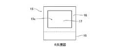
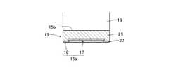
図1は、本発明の第1の実施形態に係るパワー半導体モジュール1を示す外観斜視図である。また、図2は、パワー半導体モジュール1の等価回路図である。更に、図3は、パワー半導体モジュール1の外部導出端子部10を示す外観斜視図、図4は外部導出端子部10の負極端子12を示す外観斜視図である。また、図5は、図4のR矢視図、図6は図4のA−A’線断面図である。[First Embodiment]
FIG. 1 is an external perspective view showing a power semiconductor module 1 according to the first embodiment of the present invention. FIG. 2 is an equivalent circuit diagram of the power semiconductor module 1. 3 is an external perspective view showing the external lead-out
図1に示すように、本発明の第1の実施形態に係るパワー半導体モジュール1は、例えばベース基板3上に搭載されたU相、V相及びW相のパワー半導体素子である三相インバータ回路(図示せず)を搭載する。三相インバータ回路は、ベース基板3上に形成された図示しない配線パターンと接続される。 As shown in FIG. 1, a power semiconductor module 1 according to a first embodiment of the present invention includes a three-phase inverter circuit that is a U-phase, V-phase, and W-phase power semiconductor element mounted on a
そして、このベース基板3上の三相インバータ回路及び配線パターンには、図示は省略するが、後述するゲート電極端子、コレクタ電位信号端子並びにエミッタ電位信号端子の各種端子からなる制御信号系端子部、及び図1に示すような正極端子11、負極端子12並びに交流端子13からなる外部導出端子部10がそれぞれ接続される。 The three-phase inverter circuit and the wiring pattern on the
このように構成されたパワー半導体モジュール1は、これらベース基板3上の三相インバータ回路、制御信号系端子部及び外部導出端子部10を、例えばインサート成形により外囲樹脂ケース2でその周囲を覆った構造を有する。なお、図示は省略するが、完成形態(完成品)のパワー半導体モジュール1においては、ベース基板3の裏面側には、例えば放熱部材が配置され、外囲樹脂ケース2の内部領域はゲル状の樹脂により封止される。 The power semiconductor module 1 configured in this manner covers the periphery of the three-phase inverter circuit, the control signal system terminal portion, and the external lead-out
また、パワー半導体モジュール1の外囲樹脂ケース2は、図示しないカバーにより覆われている。そして、三相インバータ回路を構成する後述するIGBTチップやダイオードチップ等と制御信号系端子部及び外部導出端子部10とは、リボンワイヤや太線ワイヤ等のボンディングワイヤ(図示せず)によりモジュール内部で接続されている。 The surrounding resin case 2 of the power semiconductor module 1 is covered with a cover (not shown). An IGBT chip, a diode chip, etc., which will be described later, constituting the three-phase inverter circuit, and the control signal system terminal unit and the external lead-out
図1に示すパワー半導体モジュール1のベース基板3は、例えば矩形板状に形成され、このベース基板3の長手方向に沿って三相インバータ回路のU相素子、V相素子及びW相素子が配列されている。U相、V相及びW相の各相の素子には、制御信号系端子部及び外部導出端子部10がそれぞれ設けられている。 A
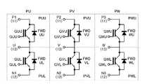
ベース基板3上の三相インバータ回路は、図1においては図示を省略しているが、図2に示すような等価回路により表されるチップにより構成され得る。この三相インバータ回路は、IGBTの直列回路と、これに並列なフリーホイールダイオードとを有してU相PU、V相PV及びW相PWの各相の素子により構成されている。 The three-phase inverter circuit on the
パワー半導体モジュール1には、図2に示すように、例えば三相インバータ回路のU相PUの上アームPUUの一部を構成する正極端子P1(11)と、下アームPULの一部を構成する負極端子N1(12)とが設けられている。また、U相PUの一部を構成する交流端子U(13)と、上アームPUUの一部を構成するゲート電極端子GUUと、下アームPULの一部を構成するゲート電極端子GULとが設けられている。なお、U相PUにおいては、正極端子P1(11)、負極端子N1(12)及び交流端子U(13)が外部導出端子部10を構成している。 As shown in FIG. 2, the power semiconductor module 1 includes, for example, a positive terminal P1 (11) constituting a part of the upper arm PUU of the U-phase PU of the three-phase inverter circuit and a part of the lower arm PUL. A negative terminal N1 (12) is provided. Further, an AC terminal U (13) constituting a part of the U-phase PU, a gate electrode terminal GUU constituting a part of the upper arm PUU, and a gate electrode terminal GUL constituting a part of the lower arm PUL are provided. It has been. In the U-phase PU, the positive terminal P1 (11), the negative terminal N1 (12), and the AC terminal U (13) constitute the external lead-out
上アームPUUのIGBTチップQUUと下アームPULのIGBTチップQULとは、直列に接続されている。また、上アームPUUのフリーホイールダイオードFWDUUは、IGBTチップQUUに並列に接続されている。更に、下アームPULのフリーホイールダイオードFWDULは、IGBTチップQULに並列に接続されている。 The IGBT chip QUU of the upper arm PUU and the IGBT chip QUL of the lower arm PUL are connected in series. The free wheel diode FWDUU of the upper arm PUU is connected in parallel to the IGBT chip QUAU. Furthermore, the free wheel diode FWDUL of the lower arm PUL is connected in parallel to the IGBT chip QUL.
なお、図示は省略するが、パワー半導体モジュール1には、IGBTチップQUU,QULのコレクタ電位を取り出すためのコレクタ電位信号端子、エミッタ電位を取り出すためのエミッタ電位信号端子、及びIGBTチップの温度検出用のサーミスタに電流を供給するための給電端子も設けられている。そして、コレクタ電位信号端子及びエミッタ電位信号端子とゲート電極端子GUU,GULとが制御信号系端子部を構成している。 Although not shown, the power semiconductor module 1 includes a collector potential signal terminal for extracting the collector potential of the IGBT chips QUAU and QUIL, an emitter potential signal terminal for extracting the emitter potential, and a temperature detection for the IGBT chip. A power supply terminal for supplying current to the thermistor is also provided. The collector potential signal terminal, the emitter potential signal terminal, and the gate electrode terminals GUU and GUL constitute a control signal system terminal portion.
同様に、パワー半導体モジュール1には、三相インバータ回路のV相PVの上アームPVUの一部を構成する正極端子P2(11)と、下アームPVLの一部を構成する負極端子N2(12)とが設けられている。また、V相PVの一部を構成する交流端子V(13)と、上アームPVUの一部を構成するゲート電極端子GVUと、下アームPVLの一部を構成するゲート電極端子GVLとが設けられている。なお、V相PVにおいては、正極端子P2(11)、負極端子N2(12)及び交流端子V(13)が外部導出端子部10を構成している。 Similarly, the power semiconductor module 1 includes a positive terminal P2 (11) constituting a part of the upper arm PVU of the V-phase PV of the three-phase inverter circuit and a negative terminal N2 (12 constituting a part of the lower arm PVL). ) And are provided. Further, an AC terminal V (13) that constitutes a part of the V-phase PV, a gate electrode terminal GVU that constitutes a part of the upper arm PVU, and a gate electrode terminal GVL that constitutes a part of the lower arm PVL are provided. It has been. In the V phase PV, the positive terminal P2 (11), the negative terminal N2 (12), and the AC terminal V (13) constitute the external lead-out
上アームPVUのIGBTチップQVUと下アームPVLのIGBTチップQVLとは、直列に接続されている。上アームPVUのフリーホイールダイオードFWDVU及び下アームPVLのフリーホイールダイオードFWDVLは、それぞれIGBTチップQVU,QVLに並列に接続されている。 The IGBT chip QVU of the upper arm PVU and the IGBT chip QVL of the lower arm PVL are connected in series. The free wheel diode FWDVU of the upper arm PVU and the free wheel diode FWDVL of the lower arm PVL are connected in parallel to the IGBT chips QVU and QVL, respectively.
また、パワー半導体モジュール1には、三相インバータ回路のW相PWの上アームPWUの一部を構成する正極端子P3(11)と、下アームPWLの一部を構成する負極端子N3(12)とが設けられている。更に、W相PWの一部を構成する交流端子W(13)と、上アームPWUの一部を構成するゲート電極端子GWUと、下アームPWLの一部を構成するゲート電極端子GWLとが設けられている。なお、W相PWにおいては、正極端子P3(11)、負極端子N3(12)及び交流端子W(13)が外部導出端子部10を構成している。 Further, the power semiconductor module 1 includes a positive terminal P3 (11) constituting a part of the upper arm PWU of the W-phase PW of the three-phase inverter circuit and a negative terminal N3 (12) constituting a part of the lower arm PWL. And are provided. Furthermore, an AC terminal W (13) constituting a part of the W-phase PW, a gate electrode terminal GWU constituting a part of the upper arm PWU, and a gate electrode terminal GWL constituting a part of the lower arm PWL are provided. It has been. In the W phase PW, the positive terminal P3 (11), the negative terminal N3 (12), and the AC terminal W (13) constitute the external lead-out
上アームPWUのIGBTチップQWUと下アームPWLのIGBTチップQWLとは、直列に接続されている。上アームPWUのフリーホイールダイオードFWDWU及び下アームPWLのフリーホイールダイオードFWDWLは、それぞれIGBTチップQWU,QWLに並列に接続されている。 The IGBT chip QWU of the upper arm PWU and the IGBT chip QWL of the lower arm PWL are connected in series. The freewheel diode FWDWU of the upper arm PWU and the freewheel diode FWDWL of the lower arm PWL are connected in parallel to the IGBT chips QWU and QWL, respectively.
なお、V相PV及びW相PWにおいても、IGBTチップQVU,QVL,QWU,QWLのコレクタ電位を取り出すためのコレクタ電位信号端子、エミッタ電位を取り出すためのエミッタ電位信号端子、及びIGBTチップの温度検出用のサーミスタに電流を供給するための給電端子もそれぞれ設けられている。そして、コレクタ電位信号端子及びエミッタ電位信号端子と、ゲート電極端子GVU,GVL及びGWU,GWLとが、それぞれV相PV及びW相PWの制御信号系端子部を構成している。 Also in the V-phase PV and W-phase PW, the collector potential signal terminal for extracting the collector potential of the IGBT chips QVU, QVL, QWU, and QWL, the emitter potential signal terminal for extracting the emitter potential, and the temperature detection of the IGBT chip Power supply terminals for supplying current to the thermistor are also provided. The collector potential signal terminal, the emitter potential signal terminal, and the gate electrode terminals GVU, GVL, GWU, and GWL constitute V-phase PV and W-phase PW control signal system terminal sections, respectively.
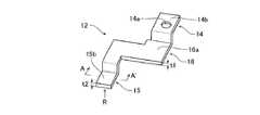
外部導出端子部10は、図3に示すように、それぞれ絶縁状態で組み合わせ配置された正極端子11、負極端子12及び交流端子13を備えて構成されている。これら正極端子11、負極端子12及び交流端子13は、形状以外はほぼ同一の構造及び構成を備えているため、以下では負極端子12を例に挙げて説明する。 As shown in FIG. 3, the external lead-out
図4に示すように、負極端子12は、銅やアルミニウムなどの金属母材21(図6参照)を打ち抜き/折り曲げ加工等して形成されている。負極端子12は、上方から見てクランク状の形状を有し、一方の端部側にケーブル等の外部機器と接続される外部接続部14が形成されている。また、負極端子12は、他方の端部側にベース基板3の配線パターンと超音波溶接により接続される基板側接続部15が形成され、これら外部接続部14及び基板側接続部15を繋いで連結する端子本体部16を有している。 As shown in FIG. 4, the
外部接続部14は、板状に形成され、その中心部に設けられたねじ挿通孔14aを備えている。端子本体部16は、外部接続部14の主面14bよりも下がった位置に主面16aを有するように形成されている。これら外部接続部14及び端子本体部16の厚さt1は、例えば1.5mmに設定されている。そして、基板側接続部15は、同じく板状に形成され、その主面15bが端子本体部16の主面16aよりも更に下がった位置にくるように形成されている。なお、主面15bは、凹凸のない平面で、後述する超音波溶接機のホーン80との第2の当接面を構成する。 The
この基板側接続部15は、例えば幅が約9mmで長さが約6mm及び厚さt2が例えば0.8mmの矩形状に形成され、図5に示すように、主面15bと反対側の裏面が、配線パターンとの第1の当接面15aを構成する。この当接面15aは、例えば凹状に形成されている。第1の当接面15aは、R矢視(平面視)で見て例えば角形の中央領域17と、その外側の外周枠状領域18とを備えて構成され、中央領域17が外周枠状領域18よりも薄くなるように形成されることで、垂直断面形状がコの字型の矩形凹状に形成されている。 The board-
基板側接続部15は、図6に示すように、例えば少なくとも第1の当接面15a側に設けられたメッキ層22を有し得る。このメッキ層22は、その厚さが2〜6μm程度のニッケル等からなる。そして、メッキ層22は、負極端子12の金属母材21と共に厚さが薄い中央領域17と外周枠状領域18とを備えた第1の当接面15aを構成する。 As shown in FIG. 6, the substrate-
外部導出端子部10の正極端子11、負極端子12及び交流端子13は、それぞれこのように構成された第1の当接面15aを有する基板側接続部15を備える。このため、ベース基板3の配線パターンとの超音波溶接の際に、外周枠状領域18から接合が開始されつつ中央領域17に集中的に荷重を掛けて超音波振動のエネルギーを集中させることができる。これにより、第1の当接面15a側の基板側接続部15の端部に集中荷重が掛かることを防いで、この端部下方の配線パターンやベース基板3への集中荷重による基板割れや破損、欠け等を防止することができる。 The
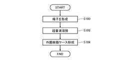
次に、このように構成されたパワー半導体モジュール1の製造工程の一部について、図7のフローチャートを参照しながら説明する。図7は、パワー半導体モジュール1の製造工程の一部を示すフローチャートである。図8は、この製造工程における超音波溶接工程を示す断面図である。 Next, a part of manufacturing process of the power semiconductor module 1 configured as described above will be described with reference to a flowchart of FIG. FIG. 7 is a flowchart showing a part of the manufacturing process of the power semiconductor module 1. FIG. 8 is a cross-sectional view showing an ultrasonic welding process in this manufacturing process.
図7に示すように、パワー半導体モジュール1は、全体の製造工程の中で、端子形成工程(ステップS100)、超音波溶接工程(ステップS102)及び外囲樹脂ケース形成工程(ステップS104)の各工程を経た上で、最終的に完成品として製造される。以下では、上記各工程について説明する。なお、ベース基板3や三相インバータ回路、制御信号系端子部を構成する各種端子等は別途作製して準備しておく。 As shown in FIG. 7, the power semiconductor module 1 includes a terminal forming process (step S100), an ultrasonic welding process (step S102), and an enclosing resin case forming process (step S104) in the entire manufacturing process. After going through the process, it is finally manufactured as a finished product. Below, each said process is demonstrated. Note that the
まず、外部導出端子部10を構成する各端子11〜13を形成する(ステップS100)。各端子11〜13は、例えば金属母材21の片面側にメッキ層22を形成し、打ち抜き/折り曲げ加工して外部接続部14、基板側接続部15及び端子本体部16を形成する。その上で、基板側接続部15を押圧加工することにより、外部接続部14及び端子本体部16よりも全体的に薄く、且つ第1の当接面15a側の中央領域17が外周枠状領域18よりも薄くされ主面15bが平面とされた基板側接続部15を形成する。 First, each terminal 11-13 which comprises the external derivation | leading-out
次に、ベース基板3上に、三相インバータ回路を搭載し、ワイヤボンディング等を施した上で、図8(a)に示すように、アンヴィル81上に載置されたベース基板3の配線パターン4上に、基板側接続部15を第1の当接面15aが配線パターン4と対向するように配置する。そして、図示しない超音波溶接機のホーン80の平面状の先端面82を基板側接続部15の主面15b上に当接させる。なお、第1の実施形態においては、ホーン80の先端面82は、中央領域17及び外周枠状領域18を含む第1の当接面15aよりも大きな面積を有するように構成されている。 Next, after mounting a three-phase inverter circuit on the
その後、ホーン80を図中矢印Bで示す方向に押し付けながら圧力を加え、図中矢印Cで示す方向に振動させて超音波溶接を施す(ステップS102)。このとき、第1の当接面15aの外周枠状領域18のメッキ層22及び金属母材21と配線パターン4との界面において金属相互の原子結合がなされる。これと共に、中央領域17にホーン80による荷重と超音波振動のエネルギーが集中して中央領域17のメッキ層22及び金属母材21と配線パターン4とが接触しその界面における金属相互の原子結合がなされる。 Thereafter, pressure is applied while pressing the
これにより、図8(b)に示すように、基板側接続部15の第1の当接面15a側の端部に集中荷重が掛からずに基板側接続部15の第1の当接面15aと配線パターン4との界面全体に亘って強固な結合層23が形成される。従って、配線パターン4と接続された基板側接続部15の当接面15a側の端部下方の割れや破損、欠けなどを防止して、接続信頼性を高めることが可能となる。 As a result, as shown in FIG. 8B, the
こうしてベース基板3の配線パターン4に外部導出端子部10の各端子11〜13を接続したら、三相インバータ回路や制御信号系端子部及び外部導出端子部10が接続されたベース基板3やねじ挿通孔14aに挿通されるねじ止め用のボルト等の各部品を所定の金型のキャビティ内にセットする。 When the
そして、PPS樹脂やPBT樹脂等の樹脂材料を金型のキャビティ内に射出して、外囲樹脂ケース2をインサート成形により形成する(ステップS104)。その後、成形品を金型のキャビティ内から取り出して、完成検査等を経てパワー半導体モジュール1が製造される。 Then, a resin material such as PPS resin or PBT resin is injected into the cavity of the mold, and the surrounding resin case 2 is formed by insert molding (step S104). Thereafter, the molded product is taken out from the cavity of the mold, and the power semiconductor module 1 is manufactured through completion inspection and the like.
以上述べたように、第1の実施形態のパワー半導体モジュール1によれば、基板側接続部15のベース基板3の配線パターン4との第1の当接面15aが、凹状となる中央領域17及び外周枠状領域18を備えている。このため、溶接の際に第1の当接面15aの端部側となる外周枠状領域18を確実に配線パターン4に接合しつつ、中央領域17に集中的に荷重を掛けて超音波振動のエネルギーを集中させて溶接を行うことができる。従って、基板側接続部15の第1の当接面15a側の端部に荷重が掛かることを防ぎ、端部下方のベース基板3の基板割れや破損、欠け等を防止して、接続信頼性を高めることができる。 As described above, according to the power semiconductor module 1 of the first embodiment, the
なお、上述した実施形態のパワー半導体モジュール1においては、パワー半導体素子として三相インバータ回路を採用したが、この三相インバータ回路はあくまで一例であるため、他の回路を採用するようにしてもよい。また、各端子11〜13の基板側接続部15は、例えば次のような第1の当接面15aを備えていてもよい。図9は、外部導出端子部10における基板側接続部15の第1の当接面15aの変形例を示す図である。図10は、外部導出端子部10における基板側接続部15の第1の当接面15aの他の変形例を示す図である。図9(a)及び図10(a)は第1の当接面15aの正面を示し、図9(b)及び図10(b)は基板側接続部15の断面を示している。 In the power semiconductor module 1 of the above-described embodiment, a three-phase inverter circuit is employed as the power semiconductor element. However, since this three-phase inverter circuit is merely an example, another circuit may be employed. . Moreover, the board | substrate
図9(a)及び(b)に示すように、変形例の第1の当接面15aは、円形且つ断面湾曲型の凹状の中央領域17及びその外周枠状領域18を有し得る。また、図10(a)及び(b)に示すように、他の変形例の第1の当接面15aは、矩形且つ最深部の断面がくの字型の凹状の中央領域17及びその外周枠状領域18を有し得る。なお、それぞれにおいて主面15bは平面状に構成されている。これらのように構成しても、上述したように荷重及び超音波振動のエネルギーを中央領域17に集中させて溶接することができるので、接続信頼性を高めることができる。 As shown in FIGS. 9A and 9B, the
また、第1の実施形態においては、基板側接続部15は、その第1の当接面15a側に中央領域17及び外周枠状領域18が設けられ且つ主面15bが平面状の矩形凹状に形成されていたが、第1の当接面15a側の中央領域17を外周枠状領域18よりも厚く形成することで矩形凸状に形成するようにしても良い。この場合においても、上記と同様の作用効果を奏することが可能である。 Further, in the first embodiment, the board-
[第2の実施形態]
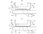
図11は、本発明の第2の実施形態に係るパワー半導体モジュール1の外部導出端子部10の負極端子12を示す外観斜視図である。また、図12は、パワー半導体モジュール1の製造工程における超音波溶接工程を示す断面図である。なお、図12は図11の基板側接続部15AにおけるB−B‘線断面部分を含んだ溶接前の状態を示しており、配線パターンの図示は省略している。図11及び図12を含む以降の説明においては、第1の実施形態と同一の構成要素に関しては同一の参照符号を付しているので、以下では重複する説明は省略する。[Second Embodiment]
FIG. 11 is an external perspective view showing the
図11に示すように、第2の実施形態においては、外部導出端子部10の端子の一例として挙げられた負極端子12の基板側接続部15Aが、平面状の第1の当接面15aと、中央領域17がその外周枠状領域18よりも薄くなるように形成された主面15bとを備えて構成されている。この点において、第1の当接面15a及び主面15bの構成が上下反対となる第1の実施形態の基板側接続部15とは相違している。 As shown in FIG. 11, in the second embodiment, the substrate-
図12に示すように、第1の当接面15a側にはメッキ層22が形成され、主面15b側の中央領域17はホーン80の先端面82よりも大きな面積で形成されている。このように構成された基板側接続部15Aを用いても、ホーン80による超音波溶接の際に、第1の当接面15a側の端部への集中荷重を無くしつつ、主面15bの中央領域17にホーン80の先端面82を確実に当接して、この中央領域17に集中的に荷重を掛け超音波振動のエネルギーを集中させて溶接を行うことができる。これにより、第1の実施形態と同様の作用効果を奏することができる。 As shown in FIG. 12, the plated
[第3の実施形態]
図13は、本発明の第3の実施形態に係るパワー半導体モジュール1の製造工程における超音波溶接工程を示す断面図である。図13は図12と同様に溶接前の状態を配線パターンの図示を省略して示している。図13に示すように、第3の実施形態においては、ホーン80の先端形状が、凸状に突出した突出部80aを有するように形成されている。この突出部80aの先端にホーン80の先端面82が設けられている。この点において、ホーン80の先端形状が平面状の先端面82であった第1及び第2の実施形態とは相違している。[Third Embodiment]
FIG. 13: is sectional drawing which shows the ultrasonic welding process in the manufacturing process of the power semiconductor module 1 which concerns on the 3rd Embodiment of this invention. FIG. 13 shows the state before welding with the wiring pattern omitted, as in FIG. As shown in FIG. 13, in the third embodiment, the tip shape of the
このように構成されたホーン80を用いれば、超音波溶接の際に、主面15b側の中央領域17の範囲内において、突出部80aの先端面82が中心辺りに当接するため、より集中的に荷重及び超音波振動のエネルギーを掛けて溶接を行うことができる。これにより、第1の当接面15a側の端部への集中荷重を無くし、基板割れや破損、欠けなどをより効果的に防止することができ、接続信頼性を高めることができる。 When the
[第4の実施形態]
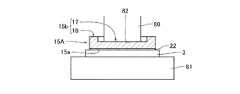
図14は、本発明の第4の実施形態に係るパワー半導体モジュール1の外部導出端子部10の負極端子12を示す外観斜視図である。また、図15は、パワー半導体モジュール1の製造工程における超音波溶接工程を示す断面図である。なお、図15は図14の基板側接続部15BにおけるC−C‘線断面部分を含んだ溶接前の状態を示しており、配線パターンの図示は省略している。図14及び図15を含む以降の説明においては、上述した実施形態と同一の構成要素については同一の参照符号を付して重複する説明は省略する。[Fourth Embodiment]
FIG. 14 is an external perspective view showing the
図14に示すように、第4の実施形態においては、外部導出端子部10の端子の一例として挙げられた負極端子12の基板側接続部15Bが、平面状の第1の当接面15aと、中央領域17がその外周枠状領域18よりも厚くなるように形成された主面15bとを備えて構成されている。この点において、中央領域17がその外周枠状領域18よりも薄くなるように形成された第2及び第3の実施形態の基板側接続部15Aとは相違している。なお、超音波溶接機のホーン80は、第3の実施形態と同様のものが用いられる。 As shown in FIG. 14, in the fourth embodiment, the substrate-
図15に示すように、第1の当接面15a側にはメッキ層22が形成され、主面15b側の中央領域17はホーン80の突出部80aの先端面82よりも小さな面積で形成されている。このように構成された基板側接続部15Bを用いても、ホーン80による超音波溶接の際に、中央領域17に集中的に荷重及び超音波振動のエネルギーを掛けて溶接を行い、第1の当接面15a側の端部への集中荷重を防ぐことができる。これにより、上述した実施形態と同様の作用効果を奏することができる。 As shown in FIG. 15, the
以上、本発明のいくつかの実施の形態を説明したが、これらの実施の形態は、例として提示したものであり、発明の範囲を限定することは意図していない。これら新規な実施の形態は、その他の様々な形態で実施されることが可能であり、発明の要旨を逸脱しない範囲で、種々の省略、置き換え、変更を行うことができる。これら実施の形態やその変形は、発明の範囲や要旨に含まれると共に、特許請求の範囲に記載された発明とその均等の範囲に含まれる。 As mentioned above, although several embodiment of this invention was described, these embodiment is shown as an example and is not intending limiting the range of invention. These novel embodiments can be implemented in various other forms, and various omissions, replacements, and changes can be made without departing from the scope of the invention. These embodiments and modifications thereof are included in the scope and gist of the invention, and are included in the invention described in the claims and the equivalents thereof.
1 パワー半導体モジュール
2 外囲樹脂ケース
3 ベース基板
4 配線パターン
10 外部導出端子部
11 正極端子
12 負極端子
13 交流端子
14 外部接続部
14a ねじ挿通孔
15 基板側接続部
15a 当接面
16 端子本体部
17 中央領域
18 外周枠状領域
21 金属母材
22 メッキ層
23 結合層DESCRIPTION OF SYMBOLS 1 Power semiconductor module 2 Surrounding
Claims (3)
Translated fromJapanese板状部材からなり前記配線パターンと接続される基板側接続部と、外部機器と接続される外部接続部とを有すると共に、前記基板側接続部の前記配線パターンとの第1 の当接面及び超音波溶接機のホーンとの第2 の当接面のいずれか一方が、中央領域がその外周枠状領域よりも薄くなる凹状又は中央領域がその外周枠状領域よりも厚くなる凸状に形成された前記外部導出端子を形成する工程と、
前記配線パターン上に前記第1 の当接面を対向配置して前記基板側接続部を超音波溶接により前記配線パターンに接続する工程とを備えた
ことを特徴とするパワー半導体モジュールの製造方法。A power semiconductor module comprising: a substrate on which a wiring pattern is formed; a power semiconductor element mounted on the substrate and connected to the wiring pattern; and an external lead terminal connected to the wiring pattern by ultrasonic welding A manufacturing method of
A board-side connection portion made of a plate-like member and connected to the wiring pattern; and an external connection portion connected to an external device; and a first contact surface of the board-side connection portion with the wiring pattern; Either one of the second contact surfaces with the horn of the ultrasonic welder is formed in a concave shape in which the central region is thinner than the outer peripheral frame-shaped region or a convex shape in which the central region is thicker than the outer peripheral frame-shaped region. Forming the external lead-out terminal,
A method of manufacturing a power semiconductor module, comprising: a step of opposingly arranging the first contact surface on the wiring pattern and connecting the substrate side connection portion to the wiring pattern by ultrasonic welding.
ことを特徴とする請求項1記載のパワー半導体モジュールの製造方法。2. The method of manufacturing a power semiconductor module according to claim 1, wherein in the step of forming the external lead-out terminal, a plating layer is formed at least on the first contact surface side of the substrate-side connection portion.
ことを特徴とする請求項1又は2記載のパワー半導体モジュールの製造方法。In the step of connecting to the wiring pattern, the front end surface of the horn formed in a convex shape is brought into contact with the central region of the second contact surface of the board-side connecting portion, and a load is applied to the central region The method of manufacturing a power semiconductor module according to claim 1, wherein ultrasonic welding is performed.
Priority Applications (1)
| Application Number | Priority Date | Filing Date | Title |
|---|---|---|---|
| JP2015221894AJP6567957B2 (en) | 2015-11-12 | 2015-11-12 | Power semiconductor module manufacturing method |
Applications Claiming Priority (1)
| Application Number | Priority Date | Filing Date | Title |
|---|---|---|---|
| JP2015221894AJP6567957B2 (en) | 2015-11-12 | 2015-11-12 | Power semiconductor module manufacturing method |
Publications (2)
| Publication Number | Publication Date |
|---|---|
| JP2017092293A JP2017092293A (en) | 2017-05-25 |
| JP6567957B2true JP6567957B2 (en) | 2019-08-28 |
Family
ID=58768661
Family Applications (1)
| Application Number | Title | Priority Date | Filing Date |
|---|---|---|---|
| JP2015221894AActiveJP6567957B2 (en) | 2015-11-12 | 2015-11-12 | Power semiconductor module manufacturing method |
Country Status (1)
| Country | Link |
|---|---|
| JP (1) | JP6567957B2 (en) |
Families Citing this family (3)
| Publication number | Priority date | Publication date | Assignee | Title |
|---|---|---|---|---|
| JP7036045B2 (en)* | 2019-01-15 | 2022-03-15 | 三菱電機株式会社 | Manufacturing method of semiconductor device |
| CN114226947B (en)* | 2021-12-30 | 2023-09-22 | 上海骄成超声波技术股份有限公司 | Terminal ultrasonic welding device and welding method |
| WO2023189265A1 (en)* | 2022-03-28 | 2023-10-05 | 富士電機株式会社 | Semiconductor module |
Family Cites Families (5)
| Publication number | Priority date | Publication date | Assignee | Title |
|---|---|---|---|---|
| JP4927391B2 (en)* | 2005-11-25 | 2012-05-09 | 東京エレクトロン株式会社 | Joining method |
| JP5134582B2 (en)* | 2009-02-13 | 2013-01-30 | 日立オートモティブシステムズ株式会社 | Connection structure and power module |
| JP2013226580A (en)* | 2012-04-26 | 2013-11-07 | Mitsubishi Electric Corp | Ultrasonic vibration joining apparatus |
| JP5916651B2 (en)* | 2013-03-19 | 2016-05-11 | 三菱電機株式会社 | Method for manufacturing power semiconductor device |
| JP6279860B2 (en)* | 2013-09-09 | 2018-02-14 | 三菱電機株式会社 | Semiconductor device |
- 2015
- 2015-11-12JPJP2015221894Apatent/JP6567957B2/enactiveActive
Also Published As
| Publication number | Publication date |
|---|---|
| JP2017092293A (en) | 2017-05-25 |
Similar Documents
| Publication | Publication Date | Title |
|---|---|---|
| TWI404177B (en) | Electric power semiconductor circuit device and method for making same | |
| CN101661893B (en) | Resin-sealed semiconductor device, manufacturing method thereof, and lead frame | |
| CN107039297B (en) | Electrode terminal, semiconductor device, and power conversion device | |
| CN107818955B (en) | Semiconductor module and method for manufacturing semiconductor module | |
| WO2012157583A1 (en) | Semiconductor device and manufacturing method thereof | |
| CN113097173B (en) | Semiconductor package and method of manufacturing the same | |
| JP2013026627A (en) | Power element package module and method for manufacturing the same | |
| JP2012059885A (en) | Method for manufacturing semiconductor device and semiconductor device | |
| JP6567957B2 (en) | Power semiconductor module manufacturing method | |
| JP6870249B2 (en) | Semiconductor devices and methods for manufacturing semiconductor devices | |
| US10497586B2 (en) | Semiconductor device and a method of manufacturing the same | |
| JP2012248907A (en) | Power semiconductor device | |
| JP2012134300A (en) | Semiconductor device | |
| KR101644913B1 (en) | Semiconductor package by using ultrasonic welding and methods of fabricating the same | |
| JP4614107B2 (en) | Semiconductor device | |
| JPWO2012046578A1 (en) | Semiconductor device and semiconductor device production method | |
| JP5458476B2 (en) | Mold package and manufacturing method thereof | |
| JP2013125825A (en) | Semiconductor device | |
| JP2012195497A (en) | Semiconductor device and manufacturing method of the same | |
| WO2019021507A1 (en) | Semiconductor device and semiconductor module | |
| JP4978445B2 (en) | Lead frame and manufacturing method of semiconductor device | |
| WO2015052880A1 (en) | Semiconductor device and method for producing same | |
| JP2009016380A (en) | Semiconductor device and manufacturing method thereof | |
| JP2010040846A (en) | Semiconductor device and method of manufacturing the same | |
| KR100271640B1 (en) | Semiconductor package and stacking structure thereof |
Legal Events
| Date | Code | Title | Description |
|---|---|---|---|
| A711 | Notification of change in applicant | Free format text:JAPANESE INTERMEDIATE CODE: A712 Effective date:20160901 | |
| A621 | Written request for application examination | Free format text:JAPANESE INTERMEDIATE CODE: A621 Effective date:20180710 | |
| A521 | Written amendment | Free format text:JAPANESE INTERMEDIATE CODE: A821 Effective date:20181115 | |
| RD02 | Notification of acceptance of power of attorney | Free format text:JAPANESE INTERMEDIATE CODE: A7422 Effective date:20181115 | |
| A977 | Report on retrieval | Free format text:JAPANESE INTERMEDIATE CODE: A971007 Effective date:20190306 | |
| A131 | Notification of reasons for refusal | Free format text:JAPANESE INTERMEDIATE CODE: A131 Effective date:20190402 | |
| A521 | Written amendment | Free format text:JAPANESE INTERMEDIATE CODE: A523 Effective date:20190531 | |
| TRDD | Decision of grant or rejection written | ||
| A01 | Written decision to grant a patent or to grant a registration (utility model) | Free format text:JAPANESE INTERMEDIATE CODE: A01 Effective date:20190716 | |
| A61 | First payment of annual fees (during grant procedure) | Free format text:JAPANESE INTERMEDIATE CODE: A61 Effective date:20190801 | |
| R150 | Certificate of patent or registration of utility model | Ref document number:6567957 Country of ref document:JP Free format text:JAPANESE INTERMEDIATE CODE: R150 |