JP6561423B2 - Thin-film magnetic connector module - Google Patents
Thin-film magnetic connector moduleDownload PDFInfo
- Publication number
- JP6561423B2 JP6561423B2JP2017528850AJP2017528850AJP6561423B2JP 6561423 B2JP6561423 B2JP 6561423B2JP 2017528850 AJP2017528850 AJP 2017528850AJP 2017528850 AJP2017528850 AJP 2017528850AJP 6561423 B2JP6561423 B2JP 6561423B2
- Authority
- JP
- Japan
- Prior art keywords
- connector module
- board
- magnetic connector
- electrodes
- magnet
- Prior art date
- Legal status (The legal status is an assumption and is not a legal conclusion. Google has not performed a legal analysis and makes no representation as to the accuracy of the status listed.)
- Active
Links
Images


Classifications
- H—ELECTRICITY
- H01—ELECTRIC ELEMENTS
- H01R—ELECTRICALLY-CONDUCTIVE CONNECTIONS; STRUCTURAL ASSOCIATIONS OF A PLURALITY OF MUTUALLY-INSULATED ELECTRICAL CONNECTING ELEMENTS; COUPLING DEVICES; CURRENT COLLECTORS
- H01R11/00—Individual connecting elements providing two or more spaced connecting locations for conductive members which are, or may be, thereby interconnected, e.g. end pieces for wires or cables supported by the wire or cable and having means for facilitating electrical connection to some other wire, terminal, or conductive member, blocks of binding posts
- H01R11/11—End pieces or tapping pieces for wires, supported by the wire and for facilitating electrical connection to some other wire, terminal or conductive member
- H01R11/30—End pieces held in contact by a magnet
- H—ELECTRICITY
- H01—ELECTRIC ELEMENTS
- H01R—ELECTRICALLY-CONDUCTIVE CONNECTIONS; STRUCTURAL ASSOCIATIONS OF A PLURALITY OF MUTUALLY-INSULATED ELECTRICAL CONNECTING ELEMENTS; COUPLING DEVICES; CURRENT COLLECTORS
- H01R13/00—Details of coupling devices of the kinds covered by groups H01R12/70 or H01R24/00 - H01R33/00
- H01R13/62—Means for facilitating engagement or disengagement of coupling parts or for holding them in engagement
- H01R13/6205—Two-part coupling devices held in engagement by a magnet
- H—ELECTRICITY
- H01—ELECTRIC ELEMENTS
- H01R—ELECTRICALLY-CONDUCTIVE CONNECTIONS; STRUCTURAL ASSOCIATIONS OF A PLURALITY OF MUTUALLY-INSULATED ELECTRICAL CONNECTING ELEMENTS; COUPLING DEVICES; CURRENT COLLECTORS
- H01R12/00—Structural associations of a plurality of mutually-insulated electrical connecting elements, specially adapted for printed circuits, e.g. printed circuit boards [PCB], flat or ribbon cables, or like generally planar structures, e.g. terminal strips, terminal blocks; Coupling devices specially adapted for printed circuits, flat or ribbon cables, or like generally planar structures; Terminals specially adapted for contact with, or insertion into, printed circuits, flat or ribbon cables, or like generally planar structures
- H01R12/70—Coupling devices
- H01R12/71—Coupling devices for rigid printing circuits or like structures
- H01R12/712—Coupling devices for rigid printing circuits or like structures co-operating with the surface of the printed circuit or with a coupling device exclusively provided on the surface of the printed circuit
- H01R12/714—Coupling devices for rigid printing circuits or like structures co-operating with the surface of the printed circuit or with a coupling device exclusively provided on the surface of the printed circuit with contacts abutting directly the printed circuit; Button contacts therefore provided on the printed circuit
- H—ELECTRICITY
- H01—ELECTRIC ELEMENTS
- H01R—ELECTRICALLY-CONDUCTIVE CONNECTIONS; STRUCTURAL ASSOCIATIONS OF A PLURALITY OF MUTUALLY-INSULATED ELECTRICAL CONNECTING ELEMENTS; COUPLING DEVICES; CURRENT COLLECTORS
- H01R13/00—Details of coupling devices of the kinds covered by groups H01R12/70 or H01R24/00 - H01R33/00
- H01R13/62—Means for facilitating engagement or disengagement of coupling parts or for holding them in engagement
- H—ELECTRICITY
- H05—ELECTRIC TECHNIQUES NOT OTHERWISE PROVIDED FOR
- H05K—PRINTED CIRCUITS; CASINGS OR CONSTRUCTIONAL DETAILS OF ELECTRIC APPARATUS; MANUFACTURE OF ASSEMBLAGES OF ELECTRICAL COMPONENTS
- H05K1/00—Printed circuits
- H05K1/02—Details
- H05K1/11—Printed elements for providing electric connections to or between printed circuits
- H05K1/115—Via connections; Lands around holes or via connections
- H05K1/116—Lands, clearance holes or other lay-out details concerning the surrounding of a via
- H—ELECTRICITY
- H01—ELECTRIC ELEMENTS
- H01R—ELECTRICALLY-CONDUCTIVE CONNECTIONS; STRUCTURAL ASSOCIATIONS OF A PLURALITY OF MUTUALLY-INSULATED ELECTRICAL CONNECTING ELEMENTS; COUPLING DEVICES; CURRENT COLLECTORS
- H01R24/00—Two-part coupling devices, or either of their cooperating parts, characterised by their overall structure
- H01R24/38—Two-part coupling devices, or either of their cooperating parts, characterised by their overall structure having concentrically or coaxially arranged contacts
Landscapes
- Engineering & Computer Science (AREA)
- Microelectronics & Electronic Packaging (AREA)
- Details Of Connecting Devices For Male And Female Coupling (AREA)
- Telephone Set Structure (AREA)
Description
Translated fromJapanese [任意の優先出願を参照することにより引用]
米国特許法施行規則1.57条の下で、本出願と共に出願された出願データシートにおいて外国又は国内優先権主張が特定される、任意の及び全ての出願が、ここで参照により組み込まれる。[Quoted by reference to any priority application]
Any and all applications for which foreign or national priority claims are specified in an application data sheet filed with this application under 35 USC 37 CFR 1.57 are hereby incorporated by reference.
[分野]
本開示は、概して、コネクタモジュールに関し、より具体的には、磁気コネクタモジュールに関する。 [関連技術の説明][Field]
The present disclosure relates generally to connector modules, and more specifically to magnetic connector modules. [Description of related technology]
様々なコネクタが、電子機器を接続し、例えば、電子機器に電力を供給し、電子機器へ、及び電子機器間でデータを伝送するために使用され、様々な型が存在する。 Various connectors are used to connect electronic devices, for example, to supply power to electronic devices, and to transmit data to and between electronic devices, and various types exist.
多くのコネクタが、例えば、ソケットから、例えば、スマートフォン、タブレットコンピュータ等のポータブル電子機器等の電子機器への、接続点間の接続の挿入方法を採用する。多くのコネクタが、接続点間のワイヤも採用する。これらのコネクタのうちのいくつかは、ワイヤの存在が原因で、使用するのに不都合であることが多く、そのようなコネクタを繰り返し使用すると、接続点に損傷を引き起こし得る。例えば、ソケットが、繰り返しの接続及び切断プロセスから損傷を受け得る。加えて、ポータブル電子機器におけるいくつかの接続点が、デバイスのサイズ及び重量を増加させ得る。更に、無線接続が、データ通信等の、いくつかの接続目的に適し得るが、それらは、例えば、効率的で高スピードの電力供給等の、他接続目的に関して現実的ではあり得ない。従って、有線ベースのコネクタ等の、既存コネクタの、これらの不要な側面に悩まされず、一方、無線接続の不要な欠点に同時に悩まされない、コネクタの必要性がある。 Many connectors employ a method of inserting connections between connection points from, for example, sockets to electronic devices such as portable electronic devices such as smartphones and tablet computers. Many connectors also employ wires between connection points. Some of these connectors are often inconvenient to use due to the presence of wires, and repeated use of such connectors can cause damage to the connection points. For example, the socket can be damaged from repeated connection and disconnection processes. In addition, some connection points in portable electronic devices can increase the size and weight of the device. Furthermore, although a wireless connection may be suitable for some connection purposes, such as data communication, they may not be realistic for other connection purposes, such as efficient and high speed power supply. Accordingly, there is a need for a connector that does not suffer from these unnecessary aspects of existing connectors, such as wired-based connectors, while not simultaneously suffering from the unnecessary shortcomings of wireless connections.
薄磁気コネクタモジュールを提供すること、及び様々なデバイスに容易に接続され得る磁気コネクタモジュールを提供することにより、本明細書で開示されている様々な実施形態が、既存のコネクタ技術のうちのいくつかの、前述の課題を解決することを目的とする。いくつかの実施形態において、磁気コネクタモジュールは、薄膜型磁気コネクタモジュールである。 By providing a thin magnetic connector module and providing a magnetic connector module that can be easily connected to a variety of devices, the various embodiments disclosed herein enable several of the existing connector technologies. It aims at solving the above-mentioned subject. In some embodiments, the magnetic connector module is a thin film magnetic connector module.
前述の課題を解決するため、いくつかの実施形態において、薄膜型磁気コネクタモジュールは、表面上に電極を形成可能であるボードとして、内部に構築される凹状部を有する前述のボードを備え、ボードの前述の他方側及びベース面上で複数の電極から構成される電極部を備え、凹状部のベース面で、及びボードの他方側で電極部を接続するためのボード孔と、前述の凹状部へと挿入される磁石と、前述の磁石上に構築される電極部とベース面との間を絶縁するためのコーティング層とを含む。 In order to solve the above-described problem, in some embodiments, a thin film type magnetic connector module includes the above-described board having a concave portion built therein as a board on which an electrode can be formed. A board hole for connecting the electrode portion on the base surface of the concave portion and on the other side of the board, and the concave portion described above. And a coating layer for insulating between the electrode portion constructed on the magnet and the base surface.
いくつかの実施形態による薄膜型磁気コネクタモジュールは、前述のボードの一方側に形成される凹状部を有し、前述のベース面に構築される電極部と接続している接続ソケットも含み得る。 A thin film magnetic connector module according to some embodiments may also include a connection socket having a recessed portion formed on one side of the board and connected to an electrode portion constructed on the base surface.
薄膜型磁気コネクタのいくつかの実施形態が、前述のボード上に単一の筐体として構築され、ボードの一方側で拡張され得、ボードとは別個に構築され、ボードの単一の表面に取り付けられ得る、翼部も含み得る。 Some embodiments of thin film type magnetic connectors can be built as a single housing on the aforementioned board and can be extended on one side of the board, built separately from the board, on a single surface of the board It can also include a wing that can be attached.
この例において、翼部は、金属材料で作られ、前述のボードに取り付けられ、前述の凹状部へと挿入されている磁石を覆う。 In this example, the wings are made of a metallic material, attached to the aforementioned board, and cover the magnets inserted into the aforementioned recessed parts.
又、複数の実施形態は、前述の翼部及び凹状部へと挿入されている磁石を覆う金属プレートを含み得る。 Embodiments may also include a metal plate that covers the magnets inserted into the wings and recesses described above.
又、前述の翼部は、孔を備える。 Moreover, the above-mentioned wing | blade part is equipped with a hole.
この例において、孔は、中心基準である前述の凹状部の中心と周方向対称を生成するために備えられる。 In this example, the hole is provided to generate a circumferential symmetry with the center of the aforementioned concave portion being the center reference.
又、前述のボードの他方側に構築される電極部は、同心円状の形状のパターン電極で構成される。 Moreover, the electrode part constructed | assembled on the other side of the above-mentioned board is comprised with the pattern electrode of a concentric shape.
いくつかの実施形態によれば、ボードの表面の凹状部に磁石が挿入され、ボードの他方側の電極部を形成することにより、前述の電極部と外部ソケット部との間の磁力を介して、外部デバイスとの電気接続が行われ、非常に薄い磁気コネクタモジュールを提供可能である。 According to some embodiments, a magnet is inserted into the concave portion of the surface of the board to form the electrode portion on the other side of the board, thereby allowing the magnetic force between the electrode portion and the external socket portion to be An electrical connection with an external device is made, and a very thin magnetic connector module can be provided.
又、いくつかの実施形態によれば、ボードの1つの表面に翼部が構築され、翼部に孔を形成することにより、本明細書で開示されている薄膜型磁気コネクタモジュールは、様々なデバイスに容易に取り付けられるよう構成される。 Also, according to some embodiments, the wings are constructed on one surface of the board and holes are formed in the wings, so that the thin film magnetic connector module disclosed herein can be Configured to be easily attached to the device.
既存のコネクタ技術の前述の欠点に対応するため、いくつかの技術が、磁気コネクタを採用する。 In order to address the aforementioned shortcomings of existing connector technology, several technologies employ magnetic connectors.
ソケットへのこの不都合及び損傷を防ぐため、磁力を利用する磁気コネクタが開発され、使用される。 In order to prevent this inconvenience and damage to the socket, a magnetic connector utilizing magnetic force has been developed and used.
例えば、韓国登録特許第1204510号において、デバイスケースの中心孔に接続されるパターン電極部は、円形ボードの一方側で同心円状の形状であり、磁石No.1が、前述のパターン電極において内部に設置され、スペーサが、前述のパターン電極と磁石No.1との間に備えられる。 For example, in Korean Patent No. 1204510, the pattern electrode portion connected to the center hole of the device case has a concentric shape on one side of the circular board. 1 is installed inside the above-mentioned pattern electrode, and the spacer is the pattern electrode and magnet No. 1 described above. 1 is provided.
又、ブラケットは、前述のパターン電極と接触するピンソケットを備え、磁石No.3は、ピンソケットの内部に設置され、磁石No.1と磁石No.3との間の磁力を介して、前述のパターン電極とピンソケットとの間の電気接続を実現する。 The bracket is provided with a pin socket that comes into contact with the pattern electrode described above. 3 is installed inside the pin socket, and magnet No. 1 and magnet no. 3, the electrical connection between the pattern electrode and the pin socket is realized.
そのような参照文書において詳述されているように、その上にパターン電極が構築される円形ボード、スペーサ及び磁石No.1は、モバイルデバイス等に電力を供給するために使用される磁気コネクタモジュールに適用可能である。 As detailed in such reference documents, the circular board, spacer and magnet no. 1 is applicable to a magnetic connector module used for supplying power to a mobile device or the like.
しかしながら、磁気コネクタモジュールが、上記の参照文書のように構築される場合、接続モジュールの厚さは、スペーサ及び磁石No.1の幅に起因して増大するのみであり得、その結果、参照文書において詳述されているような、磁気コネクタモジュールをデバイスと接続する場合に、接続されているデバイスの位置に関する欠点は、避けられない。 However, when the magnetic connector module is constructed as in the above reference document, the thickness of the connection module is the spacer and magnet no. Can only increase due to the width of 1, so that when connecting a magnetic connector module to a device, as detailed in the reference document, the disadvantages regarding the position of the connected device are: Unavoidable.
以下、いくつかの実施形態による、磁気コネクタモジュール、例えば、薄膜型磁気コネクタモジュールの様々な詳細が、複数の図面を通して説明されるであろう。添付の複数の図面の同じ参照番号は、同じコンポーネントを指定する。 In the following, various details of a magnetic connector module, eg, a thin film magnetic connector module, according to some embodiments will be described through several drawings. The same reference number in the attached drawings designates the same component.
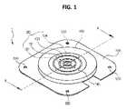
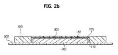
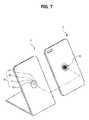
図1は、いくつかの実施形態による、薄膜型磁気コネクタモジュールの構造の設計図である。図2aは、図1上のA−A線'で分けられた薄膜型磁気コネクタモジュールの断面の第1動作例である。図2bは、図1上のA−A線'で分けられた薄膜型磁気コネクタモジュールの断面の第2動作例である。図2cは、図1上のA−A線'で分けられた薄膜型磁気コネクタモジュールの断面の第3動作例である。図3は、図2aで示されている、薄膜型磁気コネクタモジュールの第1動作例の背面図である。図4は、いくつかの実施形態の動作例による、凹状部のベース面上での電極部を示す。図5は、いくつかの実施形態の動作例による、デバイスケースと接続されている薄膜型磁気コネクタモジュールの例図である。図6a及び図6bは、いくつかの実施形態の動作例による、翼部上に設置された孔の配置を示す。図7は、デバイスケースと充填ブラケットの表面に構築され、薄膜型磁気コネクタモジュールに接続された外部ソケット部の例図である。図8は、いくつかの実施形態による、薄膜型磁気コネクタモジュールの電極部の異なる動作例の断面である。 FIG. 1 is a design diagram of a structure of a thin film magnetic connector module according to some embodiments. FIG. 2A is a first operation example of a cross section of the thin film type magnetic connector module taken along line AA ′ in FIG. FIG. 2B is a second operation example of a cross section of the thin film type magnetic connector module taken along line AA ′ in FIG. FIG. 2c is a third operation example of the cross section of the thin film type magnetic connector module taken along line AA ′ in FIG. FIG. 3 is a rear view of the first operation example of the thin film type magnetic connector module shown in FIG. 2A. FIG. 4 illustrates an electrode portion on a concave base surface, according to an example operation of some embodiments. FIG. 5 is an illustration of a thin film magnetic connector module connected to a device case, according to example operations of some embodiments. Figures 6a and 6b show the placement of holes installed on the wings, according to an example operation of some embodiments. FIG. 7 is an example of an external socket part constructed on the surface of the device case and the filling bracket and connected to the thin film type magnetic connector module. FIG. 8 is a cross-sectional view of different operation examples of electrode portions of a thin film magnetic connector module according to some embodiments.
図1から図4において示されるように、いくつかの実施形態による、薄膜型磁気コネクタモジュール1の動作例は、ボード100と、磁石200と、コーティング層300とを含み、ボード100の1つの表面の上に、接続ソケット部400及び翼部500が、様々なデバイスの、モバイルデバイス、デバイスケース等の背面カバーへの物理的な取り付けのために形成される。 As shown in FIGS. 1-4, an example of operation of a thin film magnetic connector module 1 according to some embodiments includes a
様々な実施形態によると、ボード100は、プリント回路基板(PCB)のための基板等の、電極、例えばプリント電極をその表面に形成するのに適した材料で形成される。従って、本明細書に記載の薄膜は、プリント回路基板(PCB)基板と同等の、又はより薄い厚さを指す。 According to various embodiments, the
ボード100の一方側が、凹状部110を内部に備え、磁石200は、前述の凹状部110へと挿入される。図示された実施形態において、ボード100の反対側は、平面状である。いくつかの実施形態において、磁石2001つのみが挿入される。他の実施形態において、複数の磁石が、挿入され得る。いくつかの実施形態において、磁石200は、実質的に平坦及び円形、例えば、コイン形であり、例えば、PCBボードであり得るボード100より小さい厚さを有する。 One side of the
図1−図4を参照すると、ボード100の一方側で、凹状部110のベース面115は、複数の電極121〜124を有する電極部120を備え、ボード100の他方側は、同様に、複数の電極131〜134を有する電極部130を備える。 1 to 4, on one side of the
例示を目的として、ボードの他方側に構築された電極部130は、1又は複数の電源ソケット(131(例えば、v+)、134(例えば、GND))及びデータソケット(132(例えば、D+)、133(例えば、D−))を含み得、ベース面上の電極部120は、電源ソケット(121(例えば、v+)、124(例えば、GND))及びデータソケット(122(例えば、D+)、123(例えば、D−))を含み得る。電極部130の電源ソケット(131、134)及びデータソケット(132、133)は、電極部120の電源ソケット(121、124)及びデータソケット(122、123)に対応する。しかしながら電極部120及び130を形成しているソケットは、電源ソケット及びデータソケットに限定されず、他のソケットのうち、例えば、外部ソケット部との接触をチェックするために使用されるSIGソケット等の、他のソケットを備え得ることが理解されよう。 For illustrative purposes, the
添付の複数の図面によると、ボード100の他方側に備えられる電極部130と、ベース面115に備えられる電極部120の両方は、同心円の形状で示されているが、電極部120及び130は、様々な形状で構築され得、電極部120及び130は、形状において同一である必要はない。 According to the attached drawings, both the
ボード100は、ボード100の他方側及びベース面115に構築される電極部120及び130を、電気的に接続するために使用されるボード孔140を備える。 The
ボード孔140は、ボード100の他方側の電極部130上に設置される電極131〜134上に一回以上生成され、ベース面115で電極部120を構成する電極121〜124にまで貫通される。 The
又、複数のボード孔140の内部は、例えば、導電材料でコーティングされ、又は充填されて、それらを介して形成されるコンダクタを有し、それにより、電極部120及び130は、各々、ベース面115、及びボード100の他方側にそれぞれ形成され、互いに電気的に接続される。 Further, the inside of the plurality of board holes 140 has a conductor formed, for example, by being coated or filled with a conductive material, whereby the
この例において、図4において示されるように、ベース面115に構築される電極部120は、ボード100の一方側に構築される接続ソケット部400に接続され得る。接続ソケット部400における各ソケットが、リード線(図示なし)に接続され得、そのような接続ソケット400を介して、リード線と電極部120との間の接続は、容易に達成され得る。 In this example, as shown in FIG. 4, the
1つの方法として、複数の本実施形態のうちのいくつかが使用され得、図5は、例えば、スマートフォン等のモバイルデバイスの、例えば、背面カバー等のデバイスケース2と接続されているコネクタモジュール1の例を示し、より具体的には、図面は、デバイスケース2の中心に貫通孔20を形成した後、コネクタモジュール1は、コネクタモジュール1を前述の貫通孔20に取り付けることにより、モバイルデバイスへのコネクタとして使用され得ることを示す。 As one method, some of the present embodiments may be used. FIG. 5 shows a connector module 1 connected to a device case 2 such as a back cover of a mobile device such as a smartphone. More specifically, the drawing shows that, after forming the through hole 20 at the center of the device case 2, the connector module 1 is attached to the through hole 20 to the mobile device. It can be used as a connector.
複数の実施形態によれば、コネクタモジュール1が、デバイスケース2と接続された後、デバイスケース2のいずれの側でも、高さの差異から生じるトポグラフィが最小であることが望ましい。従って、様々な実施形態において、ボード100の厚さは、デバイスケース2の厚さと実質的に同様又は同じである。従って、いくつかの実施形態において、コネクタモジュール1の少なくとも1つの表面(例えば、電極部130に対応する表面)は、ケース2の対応する面に対して面一である。つまり、電極部130を有するボード100の表面は、ケース2の外面と実質的に同一平面である表面を形成する。 According to some embodiments, it is desirable that the topography resulting from the height difference is minimal on either side of the device case 2 after the connector module 1 is connected to the device case 2. Accordingly, in various embodiments, the thickness of the
しかしながら、図5は、デバイスケース2と接続しているコネクタモジュール1の1つの動作形態を単に示し、コネクタモジュール1は、様々な他のデバイスに接続され得る。 However, FIG. 5 merely illustrates one mode of operation of the connector module 1 connected to the device case 2, and the connector module 1 can be connected to various other devices.
図5において示されるように、コネクタモジュール1をデバイスケース2と接続する場合に、ボード100がデバイスケース2上の貫通孔20へと挿入されることに従って、翼部500は、デバイスケース2の一方側に対して押し付けられ、デバイスケース2にコネクタモジュール1を固定するために使用され得る。 As shown in FIG. 5, when the connector module 1 is connected to the device case 2, the
添付の複数の図面における翼部500は、角が丸い四角形状として示されているが、翼部500は、その形状に限定されず、矩形又は円形形状として構築され得る。 Although the
いくつかの実施形態において、翼部500は、コネクタモジュール1を構築する場合に、ボード100を改変する(例えば、変形して凹状部を形成する)ことによって、ボード100の一方側から拡張する一体の部品として形成され得る。これらの実施形態において、翼部500及びボード100は、同じ材料、例えば、PCB基板で形成される。 In some embodiments, the
いくつかの他の実施形態において、翼部500は、別個に形成され、その後取り付けられ得る。別個に形成され、その後ボード100に取り付けられる場合に、翼部500は、例えば、プラスチック、合金、金属等を含む、ボードとは異なる材料で形成され得る。 In some other embodiments, the
他方では、図2aは、図1の上のA−A線'で分けられた薄膜型磁気コネクタモジュールの断面の第1動作例であり、この図によると、翼部500は、ボード100の一方側に備えられるが、翼部500は、磁石200が設置される凹状部110に備えられるようには示されない。 On the other hand, FIG. 2 a is a first operation example of a cross section of the thin film type magnetic connector module separated by line AA ′ in FIG. 1, and according to this figure, the
しかしながら、図2bにおいてコネクタモジュールの断面を示している第2動作例において示されるように、翼部500は、凹状部110へと挿入される磁石200を覆うよう構築され得る。 However, the
複数の実施形態によるボード100は、ボード100の一方側に構築される凹状部110へと、磁石200を収容するよう構成されるので、薄い磁石を有することが好ましく、従って、磁石200の磁気結合力を強める、又は磁気結合力が加えられる領域を増大させる必要があり得る。 The
磁石の磁力を強めることにおける1つの提案として、金属製の材料で作られる翼部500は、ボード100の一方側に取り付けられ得、図2bにおいて示されるように、翼部500は、凹状部110へと挿入される磁石200を覆うようにされ得る。 As one suggestion in increasing the magnet's magnetic force, a
そしてこの例において、磁石200の一方側に最も近い翼部500の領域は、磁石200の他方側に最も近いコーティング層300の領域、又はベース面115の領域より大きくなる。磁石200の磁束密度は、磁石200が最も近い側の領域に反比例する。磁石200から回路100の他方側への磁束密度は、磁石200から翼部500への磁束密度より大きくなるであろう。 In this example, the region of the
従って、金属製の翼部500が、凹状部110へと挿入される磁石200を覆う場合において、図2aにおいて示されるように、凹状部110へと挿入される磁石200を、それが覆わない場合と比べて、磁石200から回路100の他方側への方向における磁石200の磁力は、より強くなるであろう。 Accordingly, when the
又、磁石200の磁力を強めることにおける別の提案において、図2cにおいて示されるように、翼部500のより低い領域に対して別個の金属製のシート600を押し付けることにより、翼部500は、凹状部110へと挿入される磁石200を覆うようにされ得る。 Alternatively, in another proposal for increasing the magnetic force of the
同様に、金属製のシート600を追加的に加え、凹状部110へと挿入される磁石200を覆う場合に、金属製のシートがない図2aと比べて、磁石200からボード100の他方側へ方向付けられる磁石200の磁力は、より強くなるであろう、そして、この例において、金属製のシート600は、翼部500の領域全体を覆う必要はない。 Similarly, when the
いくつかの実施形態において、磁石200が翼部500の外部の主要面上に突出しないような厚さを、磁石200は、有し、ボード100の凹状部110は、そのような深さを有し、翼部500は、そのような厚さを有する。 In some embodiments, the
しかしながら、磁石200からボード100の他方側への磁束密度は、金属製のシート600の領域が増大するにつれて増大するので、金属製のシートの領域は、コネクタモジュール1によって必要とされる磁力強度を考慮して決定されなくてはならない。又、コネクタモジュール1の厚さが増大することを回避するため、金属製のシートが薄膜の形態であることが望ましい。 However, since the magnetic flux density from the
加えて、ボード100の一方側に構築される接続ソケット400からリード線への容易な接続を達成するため、接続ソケット400が設置される翼部500における間隙が生成され得る。 In addition, in order to achieve an easy connection from the
又、翼部500は、コネクタモジュール1をデバイスケース2に固定するため、複数の孔550と共に構築され得る。 Further, the
図5において示されるように、コネクタモジュール1をデバイスケース2に接続する場合において、翼部500は、デバイスケース2の一方側に対して押し付けられるであろう。この例において、コネクタモジュール1は、コネクタモジュール1の翼部500を接着剤でコーティングすること、又は孔550を介してねじ又はボルトを差し込むことを介して、デバイスケース2に取り付けられ得る。加えて、デバイスケース2の一方側に突起(図示なし)を形成すること、及びそれらを複数の孔550へと挿入すること、次に、上記突起を結合させることにより、コネクタモジュール1は、デバイスケース2に固定され得る。 As shown in FIG. 5, when connecting the connector module 1 to the device case 2, the
翼部500に設置される、単一の孔550によって、コネクタモジュール1をデバイスケース2に固定する場合において、コネクタモジュール1及びデバイスケース2は、正しく接続され得ない。従って、翼部500に複数の孔550を形成することが望ましい。 When the connector module 1 is fixed to the device case 2 by the
この例において、翼部500における複数の孔550が、ボード100の一方側に基準として構築される凹状部110の中心と、円周において対称であることが望ましい。 In this example, it is desirable that the plurality of
例えば、図6aにおいて示される場合において、翼部500に3つの孔550がある場合、それらは、中心基準として、凹状部110と120度で生成されるべきであり、翼部500に4つの孔550がある、図6bにおいて示される場合において、それらは、中心基準として、凹状部110と90度で生成されるべきである。 For example, in the case shown in FIG. 6a, if there are three
同様に、複数の孔550が、中心基準として、凹状部110の中心と周方向対称をもって生成される場合、複数の孔550によって、コネクタモジュール1を固定する場合にデバイスケース2から受ける強度は、均等に分散され得、コネクタモジュール1とデバイスケース2との間の安定した接続をもたらす。 Similarly, when the plurality of
図7は、デバイスケースと充填ブラケットの表面に構築され、薄膜型磁気コネクタモジュールに接続された外部ソケット部の例図である。 FIG. 7 is an example of an external socket part constructed on the surface of the device case and the filling bracket and connected to the thin film type magnetic connector module.
ボード100の他方側に構築される電極部130は、図7において示されるように、デバイスケース2の後方側と同じ側に構築され、外部デバイスに備えられる外部ソケット部30からの磁力による接触と電気的に接続する。 As shown in FIG. 7, the
この例において、いくつかの実施形態を参照して参照される外部デバイスは、図7において示される充填ブラケット3等の、接続モジュール1に外部電源を供給可能なデバイスを指し、外部ソケット部30は、前述の外部デバイスに備えられる電極部130からの磁力により、接触して電気的に接続し得る外部ソケットを指す。 In this example, an external device referred to with reference to some embodiments refers to a device capable of supplying external power to the connection module 1, such as the filling bracket 3 shown in FIG. This refers to an external socket that can be contacted and electrically connected by a magnetic force from the
前述のように、電極部130は、電源ソケット131(v+)、134(GND)及びデータソケット132(D+)、133(D−)から構成され得る。 As described above, the
この例において、外部ソケット30は、上記の電極部130に対応する、電源ソケット31(v+)、34(GND)及びデータソケット32(D+)、33(D−)から構成され得、電極部130が、外部ソケット30と磁気的に接続するために、別個の磁石(図示なし)が、外部ソケット30の内部に配設される。従って、外部ソケット30及び電極部130は、それらの間の磁力によって、直接の物理的な接触状態で保持されるよう構成される。 In this example, the external socket 30 may be composed of power sockets 31 (v +) and 34 (GND) and data sockets 32 (D +) and 33 (D−) corresponding to the
追加的に、電極部130の形状に関して、添付の設計図は、電極部130を、同心円状の形状であるパターン電極131〜134から構成されるものとして示すが、上記パターン電極131〜134は、同心円形パターンで構築される必要はなく、例えば、横方向に対称であるなど、パターニングが一貫性のあるものである限り、全ての形状へとパターニングされることが可能である。 In addition, regarding the shape of the
しかしながら、同心円状パターン電極131〜134が、ランダムな方向に回転される場合であっても、対応する外部ソケット30との電気接続は、維持される。 However, even when the
この例において、図8において示されるように、同心円状パターン電極131〜134の概念は、連続的な円形パターンを形成することのみならず、非連続的な円形パターンを形成することのシナリオも含む。しかしながら、非連続的パターン電極131〜134は、いくつかの実施形態を通じて、電極部130と外部ソケット30との磁気接触の間、並びに接触の後、コネクタモジュール1を回転させることにおいて限定される。 In this example, as shown in FIG. 8, the concept of concentric circular pattern electrodes 131-134 includes not only a continuous circular pattern but also a scenario of forming a discontinuous circular pattern. . However, the non-continuous pattern electrodes 131-134 are limited in some embodiments in rotating the connector module 1 during and after magnetic contact between the
追加的に、同心円状パターン電極131〜134に磁気的に接続される外部ソケット30が、外部デバイス上でピンを備える外部ピンソケットであることが望ましいが、これに限定されない。 In addition, the external socket 30 magnetically connected to the
しかしながら、外部ソケット部が外部ピンソケットである場合において、外部ピンソケットの一部が、充填ブラケット3上に生成される孔を介して外部に突出し、前述の同心円状パターン電極131〜134に1:1で対応するよう配置される。 However, when the external socket portion is an external pin socket, a part of the external pin socket protrudes to the outside through a hole generated on the filling bracket 3, and the above-mentioned
磁石200は、ボード100の一方側に構築される凹状部110へと挿入され、ボード100の他方側の電極部130を、外部デバイス上に構築される外部ソケット30に磁気的に取り付け、その2つの間に電気接続を実現する。 The
同様に、磁石200をボード100の一方側に構築される凹状部110に挿入し、ボード100の他方側に電極部130を備えることにより、いくつかの実施形態の目的である、薄膜型磁気コネクタモジュールが、提供され得る。 Similarly, the thin film magnetic connector, which is the object of some embodiments, is provided by inserting the
この例において、凹状部110へと挿入されている磁石200の厚さは、ベース面115からボード100の一方側への深さ、又はベース面115から翼部500への深さより大きくないことが望ましいが、それは、磁石200の磁力を強めるため、より大きくなり得る。 In this example, the thickness of the
しかしながら、磁石200があまりに厚い場合において、例えば、図7において示されるようにモバイルデバイスにデバイスケース2が接続している間、デバイスとの接続は、磁石200に起因して困難であると判明し得、接続した後でさえ、デバイスケース2とモバイルデバイスとの間に間隙が生成される。従って、磁石200の厚さは、コネクタモジュール1によって必要とされる磁力と、コネクタモジュール1の動作構造を考慮して決定されるべきである。 However, when the
追加的に、コーティング層は、凹状部110のベース面115に生成される。 In addition, a coating layer is created on the
電極部120が、凹状部110のベース面115に構築されるので、磁石200が凹状部110へと挿入される場合に、電極部120を構成する複数の電極121〜124の間で、電気ショートが起こる。 Since the
従って、電気ショートを防ぐため、本開示のいくつかの実施形態が、コーティング層300を含み、磁石200と電極部120との間の電気絶縁を提供する。 Thus, to prevent electrical shorts, some embodiments of the present disclosure include a
この例において、コーティング層300は、凹状部110のベース面115をコーティングすることによって、又は磁石200をコーティングすることによって生成され得る。 In this example, the
本発明は、複数の動作例に限定されず、様々な応用を有し、その特許請求の範囲が要求された本発明の要点から離れること無く、本発明の技術分野における通常の知識を有する者は、様々な改良を実行し得る。 The present invention is not limited to a plurality of operation examples, has various applications, and has a general knowledge in the technical field of the present invention without departing from the essential points of the present invention as claimed. Can implement various improvements.
1・・・薄型磁気コネクタモジュール、100・・・ボード、110・・・凹状部、115・・・凹状部のベース面、120・・・ベース面に構築された電極部、130・・・ボードの一方側に構築された電極部、140・・・ボード孔、200・・・磁石、300・・・コーティング層、400・・・接続ソケット部、500・・・翼部、550・・・孔、600・・・金属製のシートDESCRIPTION OF SYMBOLS 1 ... Thin magnetic connector module, 100 ... Board, 110 ... Concave part, 115 ... Base surface of a concave part, 120 ... Electrode part built in base surface, 130 ... Board Electrode unit constructed on one side of 140, 140 ... board hole, 200 ... magnet, 300 ... coating layer, 400 ... connection socket part, 500 ... wing part, 550 ... hole , 600 ... Metal sheet
Claims (17)
Translated fromJapanese前記第1側面と反対の前記ボードの第2側面で、前記ベース面から反対の方向を向く後方表面に形成される複数の第2電極と、
前記凹状部を介して形成され、それを介して前記複数の第1電極と前記複数の第2電極とを電気的に接続するために形成されるコンダクタを有する複数の孔と、
前記凹状部に配設される磁石と、
前記磁石と前記複数の第1電極との間に介在する絶縁層と
を備える
磁気コネクタモジュール。A board having a concave portion formed on a first side surface, the concave portion including a base surface including a plurality of first electrodes formed thereon; and
A plurality of second electrodes formed on a rear surface facing away from the base surface on a second side of the board opposite the first side;
A plurality of holes having conductors formed to electrically connect the plurality of first electrodes and the plurality of second electrodes through the concave portions;
A magnet disposed in the concave portion;
A magnetic connector module comprising: an insulating layer interposed between the magnet and the plurality of first electrodes.
前記孔を介して挿入される磁気コネクタモジュールを備え、前記磁気コネクタモジュールは、
第1側面に形成される凹状部を有するボードであって、前記凹状部は、そこに形成される複数の第1電極を含むベース面を含む、ボードと、
前記第1側面と反対の前記ボードの第2側面で、及び前記ベース面から反対の方向を向く後方表面に形成される複数の第2電極と、
前記凹状部を介して形成され、それを介して前記複数の第1電極と前記複数の第2電極とを電気的に接続するために形成されるコンダクタを有する複数の孔と、
前記凹状部に配設される磁石と、
前記磁石と前記複数の第1電極との間に介在する絶縁層と
を有する
デバイスケースアセンブリ。A device casing having holes formed therethrough;
The magnetic connector module is inserted through the hole, the magnetic connector module,
A board having a concave portion formed on a first side surface, the concave portion including a base surface including a plurality of first electrodes formed thereon; and
A plurality of second electrodes formed on a second side of the board opposite to the first side and on a rear surface facing away from the base surface;
A plurality of holes having conductors formed to electrically connect the plurality of first electrodes and the plurality of second electrodes through the concave portions;
A magnet disposed in the concave portion;
A device case assembly comprising: an insulating layer interposed between the magnet and the plurality of first electrodes.
Applications Claiming Priority (5)
| Application Number | Priority Date | Filing Date | Title |
|---|---|---|---|
| KR2020140008618UKR200489678Y1 (en) | 2014-11-25 | 2014-11-25 | Thin film type magnetic connector module |
| KR20-2014-0008618 | 2014-11-25 | ||
| US14/948,724US9620893B2 (en) | 2014-11-25 | 2015-11-23 | Thin film type magnetic connector module |
| US14/948,724 | 2015-11-23 | ||
| PCT/US2015/062522WO2016086055A1 (en) | 2014-11-25 | 2015-11-24 | Thin film type magnetic connector module |
Publications (2)
| Publication Number | Publication Date |
|---|---|
| JP2017537442A JP2017537442A (en) | 2017-12-14 |
| JP6561423B2true JP6561423B2 (en) | 2019-08-21 |
Family
ID=56006441
Family Applications (1)
| Application Number | Title | Priority Date | Filing Date |
|---|---|---|---|
| JP2017528850AActiveJP6561423B2 (en) | 2014-11-25 | 2015-11-24 | Thin-film magnetic connector module |
Country Status (6)
| Country | Link |
|---|---|
| US (3) | US9620893B2 (en) |
| EP (1) | EP3224911B1 (en) |
| JP (1) | JP6561423B2 (en) |
| KR (1) | KR200489678Y1 (en) |
| CN (2) | CN105633704B (en) |
| WO (1) | WO2016086055A1 (en) |
Families Citing this family (14)
| Publication number | Priority date | Publication date | Assignee | Title |
|---|---|---|---|---|
| JP2015049717A (en)* | 2013-09-02 | 2015-03-16 | タイコエレクトロニクスジャパン合同会社 | Connector, connector assembly and wireless communication module |
| KR200489678Y1 (en)* | 2014-11-25 | 2019-07-23 | (주)에스피에스 | Thin film type magnetic connector module |
| FR3038460B1 (en)* | 2015-07-01 | 2019-09-13 | Gulplug | ELECTRICAL SOCKET ASSEMBLY |
| US10218113B2 (en)* | 2016-09-29 | 2019-02-26 | Ideal Industries, Inc. | Low voltage bus system |
| US10468818B2 (en)* | 2017-01-20 | 2019-11-05 | Philip Giampi | Magnetically activated power socket and plug combination |
| CN106877069B (en)* | 2017-03-20 | 2022-12-20 | 深圳市共济科技股份有限公司 | Connector is inhaled to magnetism and double entry magnetism is inhaled connector |
| WO2018182246A1 (en)* | 2017-03-28 | 2018-10-04 | (주)오상헬스케어 | Connector module and electronic device comprising same |
| TWI636630B (en)* | 2017-08-22 | 2018-09-21 | 中國探針股份有限公司 | 360 degree multi-directional magnetic socket |
| US11527909B2 (en) | 2018-05-11 | 2022-12-13 | Assembled Products Corporation | Magnetic charging device |
| CN111443099B (en)* | 2018-12-27 | 2024-04-16 | 深圳迈瑞生物医疗电子股份有限公司 | Flat panel detector support, X-ray imaging system sensor unit and flat panel detector |
| JP2021005513A (en)* | 2019-06-27 | 2021-01-14 | 株式会社オートネットワーク技術研究所 | Connector device |
| KR102243156B1 (en) | 2019-07-08 | 2021-04-21 | 서울과학기술대학교 산학협력단 | Snap-on coaxial connector |
| CN110933563B (en)* | 2019-11-22 | 2021-02-19 | 歌尔股份有限公司 | Sound generating device module and electronic product |
| US11417987B2 (en)* | 2019-11-25 | 2022-08-16 | Northeastern University | Magnetic matrix connector for high density, soft neural interface |
Family Cites Families (21)
| Publication number | Priority date | Publication date | Assignee | Title |
|---|---|---|---|---|
| US3588255A (en) | 1968-03-12 | 1971-06-28 | Technidyne Inc | Optical alignment methods and means utilizing coordinated laser beams and laser beam coordinating means for same |
| US3521216A (en)* | 1968-06-19 | 1970-07-21 | Manuel Jerair Tolegian | Magnetic plug and socket assembly |
| US3808577A (en)* | 1973-03-05 | 1974-04-30 | W Mathauser | Magnetic self-aligning quick-disconnect for a telephone or other communications equipment |
| US4112941A (en)* | 1977-01-06 | 1978-09-12 | Minnesota Mining And Manufacturing Company | Electrode and magnetic connector assembly |
| JPH0480991A (en) | 1990-07-24 | 1992-03-13 | Cmk Corp | Manufacture of printed wiring board |
| JP2594229Y2 (en)* | 1991-03-22 | 1999-04-26 | 三洋電機株式会社 | DC connector |
| JPH10223447A (en)* | 1997-02-04 | 1998-08-21 | Mitsubishi Electric Corp | Cored sheet, sheet coil using the same, and electric device using the sheet coil |
| JP2001352597A (en)* | 2000-06-09 | 2001-12-21 | Nec Saitama Ltd | Electro/acoustic converter having back terminal |
| KR101185377B1 (en)* | 2011-02-16 | 2012-09-26 | 주식회사 엑셀웨이 | Flat type speaker having damper-lead plate of pcb voice coil plate |
| KR101204510B1 (en) | 2012-07-09 | 2012-11-26 | (주)에스피에스 | Charging device for mobile phone |
| US8894419B1 (en)* | 2012-08-14 | 2014-11-25 | Bby Solutions, Inc. | Magnetically connected universal computer power adapter |
| KR200467719Y1 (en)* | 2012-08-31 | 2013-07-01 | (주)에스피에스 | Back cover for mobile phone |
| CN104884123B (en)* | 2012-12-21 | 2017-10-20 | 皇家飞利浦有限公司 | Magnetic Connector Assembly |
| KR101265730B1 (en)* | 2013-02-20 | 2013-05-21 | (주)에스피에스 | Magnetic connector module having a circuit for restricting power supply |
| US9678537B2 (en)* | 2013-04-30 | 2017-06-13 | Victor Kupferstein | Mobile device case and peripheral system |
| US9300083B2 (en)* | 2013-09-30 | 2016-03-29 | Apple Inc. | Stackable magnetically-retained connector interface |
| CN106463871B (en)* | 2014-04-10 | 2019-05-17 | 施恩禧电气有限公司 | Electrical connection system with ring contact |
| CN203911534U (en)* | 2014-05-28 | 2014-10-29 | 黄河科技学院 | Contact cell phone wireless charging device |
| US9531118B2 (en)* | 2014-07-10 | 2016-12-27 | Norman R. Byrne | Electrical power coupling with magnetic connections |
| KR200489678Y1 (en)* | 2014-11-25 | 2019-07-23 | (주)에스피에스 | Thin film type magnetic connector module |
| TWI636630B (en) | 2017-08-22 | 2018-09-21 | 中國探針股份有限公司 | 360 degree multi-directional magnetic socket |
- 2014
- 2014-11-25KRKR2020140008618Upatent/KR200489678Y1/ennot_activeExpired - Fee Related
- 2015
- 2015-11-23USUS14/948,724patent/US9620893B2/enactiveActive
- 2015-11-24EPEP15862208.4Apatent/EP3224911B1/enactiveActive
- 2015-11-24JPJP2017528850Apatent/JP6561423B2/enactiveActive
- 2015-11-24WOPCT/US2015/062522patent/WO2016086055A1/enactiveApplication Filing
- 2015-11-25CNCN201510835922.9Apatent/CN105633704B/enactiveActive
- 2015-11-25CNCN201520954124.3Upatent/CN205264934U/enactiveActive
- 2017
- 2017-04-10USUS15/483,487patent/US9960532B2/enactiveActive
- 2018
- 2018-04-30USUS15/967,304patent/US10461465B2/enactiveActive
Also Published As
| Publication number | Publication date |
|---|---|
| US10461465B2 (en) | 2019-10-29 |
| CN205264934U (en) | 2016-05-25 |
| EP3224911B1 (en) | 2020-10-07 |
| KR200489678Y1 (en) | 2019-07-23 |
| US20160149339A1 (en) | 2016-05-26 |
| KR20160001886U (en) | 2016-06-02 |
| EP3224911A4 (en) | 2018-06-27 |
| US9960532B2 (en) | 2018-05-01 |
| US20180248308A1 (en) | 2018-08-30 |
| CN105633704A (en) | 2016-06-01 |
| WO2016086055A1 (en) | 2016-06-02 |
| JP2017537442A (en) | 2017-12-14 |
| CN105633704B (en) | 2018-06-15 |
| EP3224911A1 (en) | 2017-10-04 |
| US9620893B2 (en) | 2017-04-11 |
| US20170214176A1 (en) | 2017-07-27 |
Similar Documents
| Publication | Publication Date | Title |
|---|---|---|
| JP6561423B2 (en) | Thin-film magnetic connector module | |
| JP2013532351A5 (en) | ||
| US9033739B2 (en) | Techniques for shielding connectors that allow for conformal coating against corrosion | |
| US20150207268A1 (en) | Dual orientation electical connector assembly | |
| CN105325064B (en) | Electronic device | |
| CN204560022U (en) | Circuit board structure with embedded connector | |
| WO2018018944A1 (en) | Mobile terminal | |
| CN105264715B (en) | Improved supports for various types of items | |
| US9437960B2 (en) | Dustproof cover for charging port of electronic device and charging base corresponding to dustproof cover | |
| CN205883335U (en) | Mobile equipment | |
| TWI583069B (en) | Connection assembly and electronic device using the same | |
| CN105704271A (en) | Mobile terminal | |
| CN203950950U (en) | Flexible flat cable connector | |
| CN107613641B (en) | PCB assembly and mobile terminal with same | |
| CN206301983U (en) | Multi-pin connector | |
| CN210297779U (en) | Electronic equipment | |
| CN204045785U (en) | Flexible flat cable connector | |
| JP2017121039A (en) | Antenna assembly | |
| CN202395234U (en) | Magnet connector | |
| CN203277883U (en) | Connector with a locking member | |
| JP3214081U (en) | Electrical terminal board for information communication | |
| CN106026304A (en) | Mobile terminal | |
| CN103647194A (en) | Active connector and communication device having same | |
| TWM494456U (en) | Circuit board structure having built-in connector | |
| CN105514643B (en) | Electric connector and its manufacturing method, electric coupler component |
Legal Events
| Date | Code | Title | Description |
|---|---|---|---|
| A621 | Written request for application examination | Free format text:JAPANESE INTERMEDIATE CODE: A621 Effective date:20181122 | |
| A871 | Explanation of circumstances concerning accelerated examination | Free format text:JAPANESE INTERMEDIATE CODE: A871 Effective date:20181205 | |
| A975 | Report on accelerated examination | Free format text:JAPANESE INTERMEDIATE CODE: A971005 Effective date:20190131 | |
| A871 | Explanation of circumstances concerning accelerated examination | Free format text:JAPANESE INTERMEDIATE CODE: A871 Effective date:20190308 | |
| TRDD | Decision of grant or rejection written | ||
| A975 | Report on accelerated examination | Free format text:JAPANESE INTERMEDIATE CODE: A971005 Effective date:20190424 | |
| A01 | Written decision to grant a patent or to grant a registration (utility model) | Free format text:JAPANESE INTERMEDIATE CODE: A01 Effective date:20190507 | |
| A601 | Written request for extension of time | Free format text:JAPANESE INTERMEDIATE CODE: A601 Effective date:20190604 | |
| A711 | Notification of change in applicant | Free format text:JAPANESE INTERMEDIATE CODE: A711 Effective date:20190705 | |
| A61 | First payment of annual fees (during grant procedure) | Free format text:JAPANESE INTERMEDIATE CODE: A61 Effective date:20190705 | |
| A521 | Request for written amendment filed | Free format text:JAPANESE INTERMEDIATE CODE: A821 Effective date:20190705 | |
| R150 | Certificate of patent or registration of utility model | Ref document number:6561423 Country of ref document:JP Free format text:JAPANESE INTERMEDIATE CODE: R150 | |
| R250 | Receipt of annual fees | Free format text:JAPANESE INTERMEDIATE CODE: R250 | |
| R250 | Receipt of annual fees | Free format text:JAPANESE INTERMEDIATE CODE: R250 | |
| R250 | Receipt of annual fees | Free format text:JAPANESE INTERMEDIATE CODE: R250 | |
| R250 | Receipt of annual fees | Free format text:JAPANESE INTERMEDIATE CODE: R250 |