JP6549976B2 - Touch detection device and display device with touch detection function - Google Patents
Touch detection device and display device with touch detection functionDownload PDFInfo
- Publication number
- JP6549976B2 JP6549976B2JP2015232252AJP2015232252AJP6549976B2JP 6549976 B2JP6549976 B2JP 6549976B2JP 2015232252 AJP2015232252 AJP 2015232252AJP 2015232252 AJP2015232252 AJP 2015232252AJP 6549976 B2JP6549976 B2JP 6549976B2
- Authority
- JP
- Japan
- Prior art keywords
- touch detection
- electrode
- drive
- substrate
- display
- Prior art date
- Legal status (The legal status is an assumption and is not a legal conclusion. Google has not performed a legal analysis and makes no representation as to the accuracy of the status listed.)
- Active
Links
Images


Classifications
- G—PHYSICS
- G06—COMPUTING OR CALCULATING; COUNTING
- G06F—ELECTRIC DIGITAL DATA PROCESSING
- G06F3/00—Input arrangements for transferring data to be processed into a form capable of being handled by the computer; Output arrangements for transferring data from processing unit to output unit, e.g. interface arrangements
- G06F3/01—Input arrangements or combined input and output arrangements for interaction between user and computer
- G06F3/03—Arrangements for converting the position or the displacement of a member into a coded form
- G06F3/041—Digitisers, e.g. for touch screens or touch pads, characterised by the transducing means
- G06F3/0412—Digitisers structurally integrated in a display
- G—PHYSICS
- G02—OPTICS
- G02F—OPTICAL DEVICES OR ARRANGEMENTS FOR THE CONTROL OF LIGHT BY MODIFICATION OF THE OPTICAL PROPERTIES OF THE MEDIA OF THE ELEMENTS INVOLVED THEREIN; NON-LINEAR OPTICS; FREQUENCY-CHANGING OF LIGHT; OPTICAL LOGIC ELEMENTS; OPTICAL ANALOGUE/DIGITAL CONVERTERS
- G02F1/00—Devices or arrangements for the control of the intensity, colour, phase, polarisation or direction of light arriving from an independent light source, e.g. switching, gating or modulating; Non-linear optics
- G02F1/01—Devices or arrangements for the control of the intensity, colour, phase, polarisation or direction of light arriving from an independent light source, e.g. switching, gating or modulating; Non-linear optics for the control of the intensity, phase, polarisation or colour
- G02F1/13—Devices or arrangements for the control of the intensity, colour, phase, polarisation or direction of light arriving from an independent light source, e.g. switching, gating or modulating; Non-linear optics for the control of the intensity, phase, polarisation or colour based on liquid crystals, e.g. single liquid crystal display cells
- G02F1/133—Constructional arrangements; Operation of liquid crystal cells; Circuit arrangements
- G02F1/1333—Constructional arrangements; Manufacturing methods
- G02F1/13338—Input devices, e.g. touch panels
- G—PHYSICS
- G02—OPTICS
- G02F—OPTICAL DEVICES OR ARRANGEMENTS FOR THE CONTROL OF LIGHT BY MODIFICATION OF THE OPTICAL PROPERTIES OF THE MEDIA OF THE ELEMENTS INVOLVED THEREIN; NON-LINEAR OPTICS; FREQUENCY-CHANGING OF LIGHT; OPTICAL LOGIC ELEMENTS; OPTICAL ANALOGUE/DIGITAL CONVERTERS
- G02F1/00—Devices or arrangements for the control of the intensity, colour, phase, polarisation or direction of light arriving from an independent light source, e.g. switching, gating or modulating; Non-linear optics
- G02F1/01—Devices or arrangements for the control of the intensity, colour, phase, polarisation or direction of light arriving from an independent light source, e.g. switching, gating or modulating; Non-linear optics for the control of the intensity, phase, polarisation or colour
- G02F1/13—Devices or arrangements for the control of the intensity, colour, phase, polarisation or direction of light arriving from an independent light source, e.g. switching, gating or modulating; Non-linear optics for the control of the intensity, phase, polarisation or colour based on liquid crystals, e.g. single liquid crystal display cells
- G02F1/133—Constructional arrangements; Operation of liquid crystal cells; Circuit arrangements
- G02F1/1333—Constructional arrangements; Manufacturing methods
- G02F1/1343—Electrodes
- G02F1/134309—Electrodes characterised by their geometrical arrangement
- G—PHYSICS
- G06—COMPUTING OR CALCULATING; COUNTING
- G06F—ELECTRIC DIGITAL DATA PROCESSING
- G06F3/00—Input arrangements for transferring data to be processed into a form capable of being handled by the computer; Output arrangements for transferring data from processing unit to output unit, e.g. interface arrangements
- G06F3/01—Input arrangements or combined input and output arrangements for interaction between user and computer
- G06F3/03—Arrangements for converting the position or the displacement of a member into a coded form
- G06F3/041—Digitisers, e.g. for touch screens or touch pads, characterised by the transducing means
- G06F3/0416—Control or interface arrangements specially adapted for digitisers
- G06F3/04164—Connections between sensors and controllers, e.g. routing lines between electrodes and connection pads
- G—PHYSICS
- G06—COMPUTING OR CALCULATING; COUNTING
- G06F—ELECTRIC DIGITAL DATA PROCESSING
- G06F3/00—Input arrangements for transferring data to be processed into a form capable of being handled by the computer; Output arrangements for transferring data from processing unit to output unit, e.g. interface arrangements
- G06F3/01—Input arrangements or combined input and output arrangements for interaction between user and computer
- G06F3/03—Arrangements for converting the position or the displacement of a member into a coded form
- G06F3/041—Digitisers, e.g. for touch screens or touch pads, characterised by the transducing means
- G06F3/0416—Control or interface arrangements specially adapted for digitisers
- G06F3/04166—Details of scanning methods, e.g. sampling time, grouping of sub areas or time sharing with display driving
- G—PHYSICS
- G06—COMPUTING OR CALCULATING; COUNTING
- G06F—ELECTRIC DIGITAL DATA PROCESSING
- G06F3/00—Input arrangements for transferring data to be processed into a form capable of being handled by the computer; Output arrangements for transferring data from processing unit to output unit, e.g. interface arrangements
- G06F3/01—Input arrangements or combined input and output arrangements for interaction between user and computer
- G06F3/03—Arrangements for converting the position or the displacement of a member into a coded form
- G06F3/041—Digitisers, e.g. for touch screens or touch pads, characterised by the transducing means
- G06F3/044—Digitisers, e.g. for touch screens or touch pads, characterised by the transducing means by capacitive means
- G06F3/0443—Digitisers, e.g. for touch screens or touch pads, characterised by the transducing means by capacitive means using a single layer of sensing electrodes
- G—PHYSICS
- G06—COMPUTING OR CALCULATING; COUNTING
- G06F—ELECTRIC DIGITAL DATA PROCESSING
- G06F3/00—Input arrangements for transferring data to be processed into a form capable of being handled by the computer; Output arrangements for transferring data from processing unit to output unit, e.g. interface arrangements
- G06F3/01—Input arrangements or combined input and output arrangements for interaction between user and computer
- G06F3/03—Arrangements for converting the position or the displacement of a member into a coded form
- G06F3/041—Digitisers, e.g. for touch screens or touch pads, characterised by the transducing means
- G06F3/044—Digitisers, e.g. for touch screens or touch pads, characterised by the transducing means by capacitive means
- G06F3/0445—Digitisers, e.g. for touch screens or touch pads, characterised by the transducing means by capacitive means using two or more layers of sensing electrodes, e.g. using two layers of electrodes separated by a dielectric layer
- G—PHYSICS
- G06—COMPUTING OR CALCULATING; COUNTING
- G06F—ELECTRIC DIGITAL DATA PROCESSING
- G06F3/00—Input arrangements for transferring data to be processed into a form capable of being handled by the computer; Output arrangements for transferring data from processing unit to output unit, e.g. interface arrangements
- G06F3/01—Input arrangements or combined input and output arrangements for interaction between user and computer
- G06F3/03—Arrangements for converting the position or the displacement of a member into a coded form
- G06F3/041—Digitisers, e.g. for touch screens or touch pads, characterised by the transducing means
- G06F3/044—Digitisers, e.g. for touch screens or touch pads, characterised by the transducing means by capacitive means
- G06F3/0446—Digitisers, e.g. for touch screens or touch pads, characterised by the transducing means by capacitive means using a grid-like structure of electrodes in at least two directions, e.g. using row and column electrodes
- G—PHYSICS
- G09—EDUCATION; CRYPTOGRAPHY; DISPLAY; ADVERTISING; SEALS
- G09G—ARRANGEMENTS OR CIRCUITS FOR CONTROL OF INDICATING DEVICES USING STATIC MEANS TO PRESENT VARIABLE INFORMATION
- G09G3/00—Control arrangements or circuits, of interest only in connection with visual indicators other than cathode-ray tubes
- G09G3/20—Control arrangements or circuits, of interest only in connection with visual indicators other than cathode-ray tubes for presentation of an assembly of a number of characters, e.g. a page, by composing the assembly by combination of individual elements arranged in a matrix no fixed position being assigned to or needed to be assigned to the individual characters or partial characters
- G09G3/34—Control arrangements or circuits, of interest only in connection with visual indicators other than cathode-ray tubes for presentation of an assembly of a number of characters, e.g. a page, by composing the assembly by combination of individual elements arranged in a matrix no fixed position being assigned to or needed to be assigned to the individual characters or partial characters by control of light from an independent source
- G09G3/36—Control arrangements or circuits, of interest only in connection with visual indicators other than cathode-ray tubes for presentation of an assembly of a number of characters, e.g. a page, by composing the assembly by combination of individual elements arranged in a matrix no fixed position being assigned to or needed to be assigned to the individual characters or partial characters by control of light from an independent source using liquid crystals
- G09G3/3611—Control of matrices with row and column drivers
- G09G3/3648—Control of matrices with row and column drivers using an active matrix
- G—PHYSICS
- G02—OPTICS
- G02F—OPTICAL DEVICES OR ARRANGEMENTS FOR THE CONTROL OF LIGHT BY MODIFICATION OF THE OPTICAL PROPERTIES OF THE MEDIA OF THE ELEMENTS INVOLVED THEREIN; NON-LINEAR OPTICS; FREQUENCY-CHANGING OF LIGHT; OPTICAL LOGIC ELEMENTS; OPTICAL ANALOGUE/DIGITAL CONVERTERS
- G02F1/00—Devices or arrangements for the control of the intensity, colour, phase, polarisation or direction of light arriving from an independent light source, e.g. switching, gating or modulating; Non-linear optics
- G02F1/01—Devices or arrangements for the control of the intensity, colour, phase, polarisation or direction of light arriving from an independent light source, e.g. switching, gating or modulating; Non-linear optics for the control of the intensity, phase, polarisation or colour
- G02F1/13—Devices or arrangements for the control of the intensity, colour, phase, polarisation or direction of light arriving from an independent light source, e.g. switching, gating or modulating; Non-linear optics for the control of the intensity, phase, polarisation or colour based on liquid crystals, e.g. single liquid crystal display cells
- G02F1/133—Constructional arrangements; Operation of liquid crystal cells; Circuit arrangements
- G02F1/1333—Constructional arrangements; Manufacturing methods
- G02F1/1335—Structural association of cells with optical devices, e.g. polarisers or reflectors
- G02F1/133509—Filters, e.g. light shielding masks
- G02F1/133514—Colour filters
- G—PHYSICS
- G02—OPTICS
- G02F—OPTICAL DEVICES OR ARRANGEMENTS FOR THE CONTROL OF LIGHT BY MODIFICATION OF THE OPTICAL PROPERTIES OF THE MEDIA OF THE ELEMENTS INVOLVED THEREIN; NON-LINEAR OPTICS; FREQUENCY-CHANGING OF LIGHT; OPTICAL LOGIC ELEMENTS; OPTICAL ANALOGUE/DIGITAL CONVERTERS
- G02F1/00—Devices or arrangements for the control of the intensity, colour, phase, polarisation or direction of light arriving from an independent light source, e.g. switching, gating or modulating; Non-linear optics
- G02F1/01—Devices or arrangements for the control of the intensity, colour, phase, polarisation or direction of light arriving from an independent light source, e.g. switching, gating or modulating; Non-linear optics for the control of the intensity, phase, polarisation or colour
- G02F1/13—Devices or arrangements for the control of the intensity, colour, phase, polarisation or direction of light arriving from an independent light source, e.g. switching, gating or modulating; Non-linear optics for the control of the intensity, phase, polarisation or colour based on liquid crystals, e.g. single liquid crystal display cells
- G02F1/133—Constructional arrangements; Operation of liquid crystal cells; Circuit arrangements
- G02F1/1333—Constructional arrangements; Manufacturing methods
- G02F1/1343—Electrodes
- G02F1/13439—Electrodes characterised by their electrical, optical, physical properties; materials therefor; method of making
- G—PHYSICS
- G02—OPTICS
- G02F—OPTICAL DEVICES OR ARRANGEMENTS FOR THE CONTROL OF LIGHT BY MODIFICATION OF THE OPTICAL PROPERTIES OF THE MEDIA OF THE ELEMENTS INVOLVED THEREIN; NON-LINEAR OPTICS; FREQUENCY-CHANGING OF LIGHT; OPTICAL LOGIC ELEMENTS; OPTICAL ANALOGUE/DIGITAL CONVERTERS
- G02F1/00—Devices or arrangements for the control of the intensity, colour, phase, polarisation or direction of light arriving from an independent light source, e.g. switching, gating or modulating; Non-linear optics
- G02F1/01—Devices or arrangements for the control of the intensity, colour, phase, polarisation or direction of light arriving from an independent light source, e.g. switching, gating or modulating; Non-linear optics for the control of the intensity, phase, polarisation or colour
- G02F1/13—Devices or arrangements for the control of the intensity, colour, phase, polarisation or direction of light arriving from an independent light source, e.g. switching, gating or modulating; Non-linear optics for the control of the intensity, phase, polarisation or colour based on liquid crystals, e.g. single liquid crystal display cells
- G02F1/133—Constructional arrangements; Operation of liquid crystal cells; Circuit arrangements
- G02F1/136—Liquid crystal cells structurally associated with a semi-conducting layer or substrate, e.g. cells forming part of an integrated circuit
- G02F1/1362—Active matrix addressed cells
- G02F1/136286—Wiring, e.g. gate line, drain line
- G—PHYSICS
- G02—OPTICS
- G02F—OPTICAL DEVICES OR ARRANGEMENTS FOR THE CONTROL OF LIGHT BY MODIFICATION OF THE OPTICAL PROPERTIES OF THE MEDIA OF THE ELEMENTS INVOLVED THEREIN; NON-LINEAR OPTICS; FREQUENCY-CHANGING OF LIGHT; OPTICAL LOGIC ELEMENTS; OPTICAL ANALOGUE/DIGITAL CONVERTERS
- G02F1/00—Devices or arrangements for the control of the intensity, colour, phase, polarisation or direction of light arriving from an independent light source, e.g. switching, gating or modulating; Non-linear optics
- G02F1/01—Devices or arrangements for the control of the intensity, colour, phase, polarisation or direction of light arriving from an independent light source, e.g. switching, gating or modulating; Non-linear optics for the control of the intensity, phase, polarisation or colour
- G02F1/13—Devices or arrangements for the control of the intensity, colour, phase, polarisation or direction of light arriving from an independent light source, e.g. switching, gating or modulating; Non-linear optics for the control of the intensity, phase, polarisation or colour based on liquid crystals, e.g. single liquid crystal display cells
- G02F1/133—Constructional arrangements; Operation of liquid crystal cells; Circuit arrangements
- G02F1/136—Liquid crystal cells structurally associated with a semi-conducting layer or substrate, e.g. cells forming part of an integrated circuit
- G02F1/1362—Active matrix addressed cells
- G02F1/1368—Active matrix addressed cells in which the switching element is a three-electrode device
- G—PHYSICS
- G02—OPTICS
- G02F—OPTICAL DEVICES OR ARRANGEMENTS FOR THE CONTROL OF LIGHT BY MODIFICATION OF THE OPTICAL PROPERTIES OF THE MEDIA OF THE ELEMENTS INVOLVED THEREIN; NON-LINEAR OPTICS; FREQUENCY-CHANGING OF LIGHT; OPTICAL LOGIC ELEMENTS; OPTICAL ANALOGUE/DIGITAL CONVERTERS
- G02F2201/00—Constructional arrangements not provided for in groups G02F1/00 - G02F7/00
- G02F2201/52—RGB geometrical arrangements
- G—PHYSICS
- G06—COMPUTING OR CALCULATING; COUNTING
- G06F—ELECTRIC DIGITAL DATA PROCESSING
- G06F2203/00—Indexing scheme relating to G06F3/00 - G06F3/048
- G06F2203/041—Indexing scheme relating to G06F3/041 - G06F3/045
- G06F2203/04101—2.5D-digitiser, i.e. digitiser detecting the X/Y position of the input means, finger or stylus, also when it does not touch, but is proximate to the digitiser's interaction surface and also measures the distance of the input means within a short range in the Z direction, possibly with a separate measurement setup
- G—PHYSICS
- G06—COMPUTING OR CALCULATING; COUNTING
- G06F—ELECTRIC DIGITAL DATA PROCESSING
- G06F2203/00—Indexing scheme relating to G06F3/00 - G06F3/048
- G06F2203/041—Indexing scheme relating to G06F3/041 - G06F3/045
- G06F2203/04102—Flexible digitiser, i.e. constructional details for allowing the whole digitising part of a device to be flexed or rolled like a sheet of paper
- G—PHYSICS
- G09—EDUCATION; CRYPTOGRAPHY; DISPLAY; ADVERTISING; SEALS
- G09G—ARRANGEMENTS OR CIRCUITS FOR CONTROL OF INDICATING DEVICES USING STATIC MEANS TO PRESENT VARIABLE INFORMATION
- G09G2354/00—Aspects of interface with display user
Landscapes
- Engineering & Computer Science (AREA)
- Theoretical Computer Science (AREA)
- General Engineering & Computer Science (AREA)
- Physics & Mathematics (AREA)
- General Physics & Mathematics (AREA)
- Human Computer Interaction (AREA)
- Crystallography & Structural Chemistry (AREA)
- Chemical & Material Sciences (AREA)
- Nonlinear Science (AREA)
- Computer Hardware Design (AREA)
- Computer Networks & Wireless Communication (AREA)
- Optics & Photonics (AREA)
- Mathematical Physics (AREA)
- Geometry (AREA)
- Position Input By Displaying (AREA)
- Liquid Crystal (AREA)
Description
Translated fromJapanese本発明は、タッチ検出装置、タッチ検出機能付き表示装置及びカバー部材に関する。 The present invention relates to a touch detection device, a display device with a touch detection function, and a cover member.
近年、いわゆるタッチパネルと呼ばれる、外部近接物体を検出可能なタッチ検出装置が注目されている。タッチパネルは、液晶表示装置等の表示装置上に装着又は一体化されて、タッチ検出機能付き表示装置として用いられている。このようなタッチ検出機能付き表示装置には表示領域の周辺部の額縁領域に入力機能を有するボタンを配置することが知られている。 In recent years, a touch detection device capable of detecting an external proximity object, which is called a so-called touch panel, has attracted attention. The touch panel is mounted or integrated on a display device such as a liquid crystal display device and used as a display device with a touch detection function. In such a display device with a touch detection function, it is known to dispose a button having an input function in a frame area in the periphery of the display area.
このような入力用ボタンは表示領域のタッチパネルと別の部品で設計して組み合わせることもできるが、入力用ボタンをタッチパネルや表示装置の額縁領域に一体化する技術についても知られている。特許文献1は、TFT基板の額縁領域にセンサ用検出電極が設けられたタッチセンサつき表示装置が記載されている。表示領域を囲む額縁領域には個別に分離された複数のセンサ用検出電極が設けられている。 Such an input button can be designed and combined with a touch panel in the display area and another component, but there is also known a technique for integrating the input button in a touch panel or a frame area of a display device.
しかし、基板の額縁領域には、電極と接続された配線や駆動回路等が設けられる場合があり、センサ用検出電極を設けると額縁領域の幅が増大する可能性がある。 However, the frame area of the substrate may be provided with a wire connected to an electrode, a drive circuit or the like, and the width of the frame area may increase when the sensor detection electrode is provided.
本発明は、額縁領域の増大を抑制しつつ、優れた額縁検出性能を有するタッチ検出装置、タッチ検出機能付き表示装置及びカバー部材を提供することを目的とする。 An object of the present invention is to provide a touch detection device having excellent frame detection performance, a display device with a touch detection function, and a cover member while suppressing an increase in a frame area.
本発明の一態様のタッチ検出装置は、第1基板と、前記第1基板と対向する第2基板と、前記第2基板と対向するカバー基材と、前記第1基板と平行な面上の表示領域に重畳して配置される複数の第1電極と、前記カバー基材上の、前記表示領域の外側の額縁領域と重畳する場所に配置される少なくとも1つの第2電極と、を有し、前記第1電極と前記第2電極との静電容量に基づいて前記額縁領域への物体の近接または接触が感知され、前記第2電極は、前記額縁領域のいずれかの辺に沿って延在する。 A touch detection device according to one aspect of the present invention includes a first substrate, a second substrate facing the first substrate, a cover base material facing the second substrate, and a surface parallel to the first substrate. It has a plurality of first electrodes arranged to overlap the display area, and at least one second electrode arranged on the cover base material so as to overlap the frame area outside the display area. The proximity or contact of an object to the frame area is sensed based on the capacitance of the first electrode and the second electrode, and the second electrode extends along any side of the frame area. Exist.
本発明の一態様のタッチ検出機能付き表示装置は、タッチ検出装置と、前記第1基板と平行な面上の前記表示領域において、行列配置された複数の画素電極と、前記表示領域内において画像表示機能を発揮する表示機能層と、を有するタッチ検出機能付き表示装置。 A display device with a touch detection function according to an aspect of the present invention includes a touch detection device, a plurality of pixel electrodes arranged in a matrix in the display region on a plane parallel to the first substrate, and an image in the display region. A display device with a touch detection function, having a display function layer that exhibits a display function.
本発明の一態様のカバー部材は、タッチ検出装置の表面側に配置されるカバー部材であって、カバー基材と、前記カバー基材と平行な面上であって、平面視で前記表示領域の外側の額縁領域に重なる位置に配置され、前記表示領域の外周の少なくともいずれかの辺に沿って延在する電極と、を有する。 The cover member according to one aspect of the present invention is a cover member disposed on the front surface side of the touch detection device, and is a surface parallel to the cover substrate and the cover substrate, and the display area in plan view And an electrode which is disposed at a position overlapping with the outer frame area and extends along at least any one side of the outer periphery of the display area.
本発明を実施するための形態(実施形態)につき、図面を参照しつつ詳細に説明する。以下の実施形態に記載した内容により本発明が限定されるものではない。また、以下に記載した構成要素には、当業者が容易に想定できるもの、実質的に同一のものが含まれる。さらに、以下に記載した構成要素は適宜組み合わせることが可能である。なお、開示はあくまで一例にすぎず、当業者において、発明の主旨を保っての適宜変更について容易に想到し得るものについては、当然に本発明の範囲に含有されるものである。また、図面は説明をより明確にするため、実際の態様に比べ、各部の幅、厚さ、形状等について模式的に表される場合があるが、あくまで一例であって、本発明の解釈を限定するものではない。また、本明細書と各図において、既出の図に関して前述したものと同様の要素には、同一の符号を付して、詳細な説明を適宜省略することがある。 A mode (embodiment) for carrying out the present invention will be described in detail with reference to the drawings. The present invention is not limited by the contents described in the following embodiments. Further, the components described below include those which can be easily conceived by those skilled in the art and those which are substantially the same. Furthermore, the components described below can be combined as appropriate. The disclosure is merely an example, and it is naturally included within the scope of the present invention as to what can be easily conceived of by those skilled in the art as to appropriate changes while maintaining the gist of the invention. In addition, the drawings may be schematically represented as to the width, thickness, shape, etc. of each portion in comparison with the actual embodiment in order to clarify the description, but this is merely an example, and the interpretation of the present invention is not limited. It is not limited. In the specification and the drawings, the same elements as those described above with reference to the drawings already described may be denoted by the same reference numerals, and the detailed description may be appropriately omitted.
(第1の実施形態)
図1は、第1の実施形態に係るタッチ検出機能付き表示装置の一構成例を示すブロック図である。図1に示すように、タッチ検出機能付き表示装置1は、タッチ検出機能付き表示部10と、制御部11と、ゲートドライバ12と、ソースドライバ13と、駆動電極ドライバ14と、タッチ検出部40とを備えている。タッチ検出機能付き表示装置1は、タッチ検出機能付き表示部10がタッチ検出機能を内蔵した表示装置である。タッチ検出機能付き表示部10は、表示素子として液晶表示素子を用いている表示パネル20と、タッチ入力を検出するタッチ検出装置であるタッチパネル30とを一体化した装置である。なお、タッチ検出機能付き表示部10は、表示パネル20の上にタッチパネル30を装着した、いわゆるオンセルタイプの装置であってもよい。表示パネル20は、例えば、有機EL表示パネルであってもよい。First Embodiment
FIG. 1 is a block diagram showing a configuration example of a display device with a touch detection function according to the first embodiment. As shown in FIG. 1, the display device with a
表示パネル20は、後述するように、ゲートドライバ12から供給される走査信号Vscanに従って、1水平ラインずつ順次走査して表示を行う素子である。制御部11は、外部より供給された映像信号Vdispに基づいて、ゲートドライバ12、ソースドライバ13、駆動電極ドライバ14及びタッチ検出部40に対してそれぞれ制御信号を供給し、これらが互いに同期して動作するように制御する回路である。 The
ゲートドライバ12は、制御部11から供給される制御信号に基づいて、タッチ検出機能付き表示部10の表示駆動の対象となる1水平ラインを順次選択する機能を有している。 The
ソースドライバ13は、制御部11から供給される制御信号に基づいて、タッチ検出機能付き表示部10の、後述する各副画素SPixに画素信号Vpixを供給する回路である。 The
駆動電極ドライバ14は、制御部11から供給される制御信号に基づいて、タッチ検出機能付き表示部10の、後述する第1駆動電極COML1に第1駆動信号Vcomを供給する回路である。 The
タッチパネル30は、静電容量型タッチ検出の基本原理に基づいて動作し、相互静電容量方式によりタッチ検出動作を行い、表示領域に対する外部の導体の接触又は近接を検出する。タッチパネル30は、自己静電容量方式によりタッチ検出動作を行ってもよい。 The
タッチ検出部40は、制御部11から供給される制御信号と、タッチパネル30から供給される第1タッチ検出信号Vdet1に基づいて、タッチパネル30に対するタッチの有無を検出する回路である。また、タッチ検出部40は、タッチがある場合においてタッチ入力が行われた座標などを求める。このタッチ検出部40は、タッチ検出信号増幅部42と、A/D変換部43と、信号処理部44と、座標抽出部45とを備える。検出タイミング制御部46は、制御部11から供給される制御信号に基づいて、A/D変換部43と、信号処理部44と、座標抽出部45とが同期して動作するように制御する。さらに、タッチ検出部40は、駆動ドライバ48を含む。駆動ドライバ48は、後述する第2駆動電極COML2A、COML2B、COML2C、COML2Dに第2駆動信号Vdを供給する回路である。 The
上述のとおり、タッチパネル30は、静電容量型タッチ検出の基本原理に基づいて動作する。ここで、図2から図8を参照して、本実施形態のタッチ検出機能付き表示装置1の相互静電容量方式によるタッチ検出の基本原理について説明する。図2は、相互静電容量方式のタッチ検出の基本原理を説明するための、指が接触又は近接していない状態を表す説明図である。図3は、図2に示す指が接触又は近接していない状態のフリンジ電界の例を示す説明図である。図4は、図2に示す指が接触又は近接していない状態の等価回路の例を示す説明図である。図5は、相互静電容量方式のタッチ検出の基本原理を説明するための、指が接触又は近接した状態を表す説明図である。図6は、図5に示す指が接触又は近接した状態のフリンジ電界の例を示す説明図である。図7は、図5に示す指が接触又は近接した状態の等価回路の例を示す説明図である。図8は、駆動信号及びタッチ検出信号の波形の一例を表す図である。なお、以下の説明では、指が接触又は近接する場合を説明するが、指に限られず、例えばスタイラスペン等の導体を含む物体であってもよい。 As described above, the
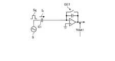
例えば、図2に示すように、容量素子C1は、誘電体Dを挟んで互いに対向配置された一対の電極、駆動電極E1及びタッチ検出電極E2を備えている。容量素子C1は、駆動電極E1とタッチ検出電極E2との対向面同士の間に形成される電気力線(図示しない)に加え、図3に示すように、駆動電極E1の端部からタッチ検出電極E2の上面に向かって延びるフリンジ分の電気力線Efが生じる。図4に示すように、容量素子C1は、その一端が交流信号源(駆動信号源)Sに接続され、他端は電圧検出器DETに接続される。電圧検出器DETは、例えば図1に示すタッチ検出信号増幅部42に含まれる積分回路である。 For example, as shown in FIG. 2, the capacitive element C1 includes a pair of electrodes arranged to face each other with the dielectric D interposed therebetween, a drive electrode E1 and a touch detection electrode E2. As shown in FIG. 3, in addition to electric lines of force (not shown) formed between opposing surfaces of drive electrode E1 and touch detection electrode E2, capacitive element C1 detects touch from the end of drive electrode E1. Electric force lines Ef of fringes extending toward the top surface of the electrode E2 are generated. As shown in FIG. 4, one end of the capacitive element C1 is connected to an alternating current signal source (drive signal source) S, and the other end is connected to a voltage detector DET. The voltage detector DET is, for example, an integration circuit included in the touch detection
交流信号源Sから駆動電極E1(容量素子C1の一端)に所定の周波数(例えば数kHz〜数百kHz程度)の交流矩形波Sgが印加されると、タッチ検出電極E2(容量素子C1の他端)側に接続された電圧検出器DETを介して、図8に示すような出力波形(第1タッチ検出信号Vdet1)が現れる。なお、この交流矩形波Sgは、駆動電極ドライバ14から入力される第1駆動信号Vcomに相当するものである。 When an alternating current rectangular wave Sg of a predetermined frequency (for example, about several kHz to several hundreds kHz) is applied from the alternating current signal source S to the drive electrode E1 (one end of the capacitive element C1), the touch detection electrode E2 (the capacitive element C1 An output waveform (first touch detection signal Vdet1) as shown in FIG. 8 appears via the voltage detector DET connected to the end) side. The AC rectangular wave Sg corresponds to the first drive signal Vcom input from the
指が接触又は近接していない状態(非接触状態)では、図4に示すように、容量素子C1に対する充放電に伴って、容量素子C1の容量値に応じた電流I0が流れる。図4に示す電圧検出器DETは、交流矩形波Sgに応じた電流I0の変動を電圧の変動(実線の波形V0(図8参照))に変換する。In a state where the finger is not in contact or in proximity (non-contact state), as shown in FIG. 4, a current I0 flows according to the capacitance value of the
一方、指が接触又は近接した状態(接触状態)では、図5に示すように、指によって形成される静電容量C2が、タッチ検出電極E2と接触している又は近傍にあることにより、図6に示すように駆動電極E1及びタッチ検出電極E2の間にあるフリンジ分の電気力線Efが遮られる。このため、容量素子C1は、図7に示すように、非接触状態での容量値よりも容量値の小さい容量素子C1’として作用する。そして、図7に示す等価回路でみると、容量素子C1’に電流I1が流れる。図8に示すように、電圧検出器DETは、交流矩形波Sgに応じた電流I1の変動を電圧の変動(点線の波形V1)に変換する。この場合、波形V1は、上述した波形V0と比べて振幅が小さくなる。これにより、波形V0と波形V1との電圧差分の絶対値|ΔV|は、指などの外部から接触又は近接する導体の影響に応じて変化することになる。なお、電圧検出器DETは、波形V0と波形V1との電圧差分の絶対値|ΔV|を精度よく検出するため、回路内のスイッチングにより、交流矩形波Sgの周波数に合わせて、コンデンサの充放電をリセットする期間Resetを設けた動作とすることがより好ましい。On the other hand, when the finger is in contact or in proximity (contact state), as shown in FIG. 5, the capacitance C2 formed by the finger is in contact with or in the vicinity of the touch detection electrode E2, as shown in FIG. As indicated by 6, the lines of electric force Ef of the fringes between the drive electrode E1 and the touch detection electrode E2 are interrupted. Therefore, as shown in FIG. 7, the capacitive element C1 acts as a capacitive element C1 ′ having a smaller capacitance value than the capacitance value in the non-contact state. When seen in the equivalent circuit shown in FIG. 7, the current I1 flows through the capacitor C1 '. As shown in FIG. 8, the voltage detector DET converts the fluctuation of the current I1 according to the AC rectangular wave Sg into a fluctuation of voltage (waveform V1 of a dotted line). In this case, the waveform V1 has a smaller amplitude than the waveform V0 described above. Thus, the absolute value | ΔV | of the voltage difference between the waveform V0 and the waveform V1 changes in accordance with the influence of an externally-contacted or adjacent conductor such as a finger. Note that the voltage detector DET accurately detects the absolute value | ΔV | of the voltage difference between the waveform V0 and the waveform V1 by switching in the circuit to match the frequency of the AC rectangular wave Sg. It is more preferable to perform an operation provided with a period Reset in which charging and discharging are reset.
図1に示すタッチパネル30は、駆動電極ドライバ14から供給される第1駆動信号Vcomに従って、1検出ブロックずつ順次走査して、相互静電容量方式によるタッチ検出を行う。 The
タッチパネル30は、後述する複数のタッチ検出電極TDLから、図3又は図5に示す電圧検出器DETを介して、検出ブロック毎に第1タッチ検出信号Vdet1を出力する。第1タッチ検出信号Vdet1は、タッチ検出部40のタッチ検出信号増幅部42に供給される。 The
タッチ検出信号増幅部42は、タッチパネル30から供給される第1タッチ検出信号Vdet1を増幅する。なお、タッチ検出信号増幅部42は、第1タッチ検出信号Vdet1に含まれる高い周波数成分(ノイズ成分)を除去して出力する低域通過アナログフィルタであるアナログLPF(Low Pass Filter)を備えていてもよい。 The touch detection
A/D変換部43は、第1駆動信号Vcom及び第2駆動信号Vdに同期したタイミングで、タッチ検出信号増幅部42から出力されるアナログ信号をそれぞれサンプリングしてデジタル信号に変換する。 The A /
信号処理部44は、A/D変換部43の出力信号に含まれる、第1駆動信号Vcom及び第2駆動信号Vdをサンプリングした周波数以外の周波数成分(ノイズ成分)を低減するデジタルフィルタを備えている。信号処理部44は、A/D変換部43の出力信号に基づいて、タッチパネル30に対するタッチの有無を検出する論理回路である。信号処理部44は、指による検出信号の差分のみ取り出す処理を行う。この指による差分の信号は、上述した波形V0と波形V1との差分の絶対値|ΔV|である。信号処理部44は、1検出ブロック当たりの絶対値|ΔV|を平均化する演算を行い、絶対値|ΔV|の平均値を求めてもよい。これにより、信号処理部44は、ノイズによる影響を低減できる。信号処理部44は、検出した指による差分の信号を所定のしきい値電圧と比較し、このしきい値電圧未満であれば、外部近接物体が非接触状態であると判断する。一方、信号処理部44は、検出した指による差分の信号を所定のしきい値電圧と比較し、しきい値電圧以上であれば、外部近接物体の接触状態と判断する。このようにして、タッチ検出部40はタッチ検出が可能となる。The
座標抽出部45は、信号処理部44においてタッチが検出されたときに、そのタッチパネル座標を求める論理回路である。座標抽出部45は、タッチパネル座標を検出信号出力Voutとして出力する。以上のように、本実施形態のタッチ検出機能付き表示装置1は、相互静電容量方式によるタッチ検出の基本原理に基づいて、指などの導体が接触又は近接する位置のタッチパネル座標を検出することができる。 The coordinate
次に、図9から図12を参照して、自己静電容量方式のタッチ検出の基本原理について説明する。図9は、自己静電容量方式のタッチ検出の基本原理を説明するための、指が接触又は近接していない状態を表す説明図である。図10は、自己静電容量方式のタッチ検出の基本原理を説明するための、指が接触又は近接した状態を表す説明図である。図11は、自己静電容量方式のタッチ検出の等価回路の例を示す説明図である。図12は、自己静電容量方式のタッチ検出の駆動信号及びタッチ検出信号の波形の一例を表す図である。 Next, the basic principle of self-capacitance touch detection will be described with reference to FIGS. 9 to 12. FIG. 9 is an explanatory view illustrating a basic principle of self-capacitive touch detection, in which a finger is not in contact with or in proximity to the touch. FIG. 10 is an explanatory view illustrating a basic principle of self-capacitive touch detection, in which a finger is in contact or in proximity. FIG. 11 is an explanatory view showing an example of an equivalent circuit of self-capacitance touch detection. FIG. 12 is a diagram illustrating an example of a drive signal of self-capacitance touch detection and a waveform of the touch detection signal.
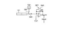
図9左図は、指が接触又は近接していない状態において、スイッチSW1により電源Vddとタッチ検出電極E2とが接続され、スイッチSW2によりタッチ検出電極E2がコンデンサCcrに接続されていない状態を示している。この状態では、タッチ検出電極E2が有する容量Cx1が充電される。図9右図は、スイッチSW1により、電源Vddとタッチ検出電極E2との接続がオフされ、スイッチSW2により、タッチ検出電極E2とコンデンサCcrとが接続された状態を示している。この状態では、容量Cx1の電荷はコンデンサCcrを介して放電される。 The left diagram in FIG. 9 shows a state in which the power supply Vdd and the touch detection electrode E2 are connected by the switch SW1 and the touch detection electrode E2 is not connected to the capacitor Ccr by the switch SW2 when the finger is not in contact or in proximity. ing. In this state, the capacitance Cx1 of the touch detection electrode E2 is charged. The right side of FIG. 9 shows a state in which the connection between the power supply Vdd and the touch detection electrode E2 is turned off by the switch SW1, and the touch detection electrode E2 and the capacitor Ccr are connected by the switch SW2. In this state, the charge of the capacitor Cx1 is discharged through the capacitor Ccr.
図10左図は、指が接触又は近接した状態において、スイッチSW1により電源Vddとタッチ検出電極E2とが接続され、スイッチSW2によりタッチ検出電極E2がコンデンサCcrに接続されていない状態を示している。この状態では、タッチ検出電極E2が有する容量Cx1に加え、タッチ検出電極E2に近接している指により生じる容量Cx2も充電される。図10右図は、スイッチSW1により、電源Vddとタッチ検出電極E2がオフされ、スイッチSW2によりタッチ検出電極E2とコンデンサCcrとが接続された状態を示している。この状態では、容量Cx1の電荷と容量Cx2の電荷とがコンデンサCcrを介して放電される。 The left diagram in FIG. 10 shows a state where the power supply Vdd and the touch detection electrode E2 are connected by the switch SW1 and the touch detection electrode E2 is not connected to the capacitor Ccr by the switch SW2 when the finger is in contact or in proximity. . In this state, in addition to the capacitance Cx1 of the touch detection electrode E2, the capacitance Cx2 generated by the finger close to the touch detection electrode E2 is also charged. The right side of FIG. 10 shows a state in which the power supply Vdd and the touch detection electrode E2 are turned off by the switch SW1, and the touch detection electrode E2 and the capacitor Ccr are connected by the switch SW2. In this state, the charge of the capacitor Cx1 and the charge of the capacitor Cx2 are discharged through the capacitor Ccr.
ここで、図9右図に示す放電時(指が接触または近接していない状態)における容量Ccrの電圧変化特性に対して、図10右図に示す放電時(指が接触又は近接した状態)における容量Ccrの電圧変化特性は、容量Cx2が存在するために、明らかに異なる。したがって、自己静電容量方式では、容量Ccrの電圧変化特性が、容量Cx2の有無により、異なることを利用して、指などの操作入力の有無を判定している。 Here, with respect to the voltage change characteristic of the capacitance Ccr at the time of discharge shown in the right view of FIG. 9 (a state where the finger is not in contact or close), at the time of discharge shown in the right view of FIG. The voltage change characteristic of the capacitance Ccr at the point C. is obviously different due to the presence of the capacitance Cx2. Therefore, in the self-capacitance method, the presence or absence of an operation input from a finger or the like is determined using the fact that the voltage change characteristic of the capacitance Ccr differs depending on the presence or absence of the capacitance Cx2.
具体的には、タッチ検出電極E2に所定の周波数(例えば数kHz〜数百kHz程度)の交流矩形波Sg(図12参照)が印加される。図11に示す電圧検出器DETは、交流矩形波Sgに応じた電流の変動を電圧の変動(波形V4、V5)に変換する。Specifically, an alternating current rectangular wave Sg (see FIG. 12) having a predetermined frequency (for example, several kHz to several hundreds kHz) is applied to the touch detection electrode E2. The voltage detector DET shown in FIG. 11 converts the fluctuation of the current according to the AC rectangular wave Sg into the fluctuation of the voltage (waveforms V4 and V5 ).
上述のように、タッチ検出電極E2はスイッチSW1及びスイッチSW2で切り離すことが可能な構成となっている。図12において、時刻T01のタイミングで交流矩形波Sgは電圧V0に相当する電圧レベルを上昇させる。このときスイッチSW1はオンしておりスイッチSW2はオフしている。このためタッチ検出電極E2の電圧も電圧V0に上昇する。次に時刻T11のタイミングの前にスイッチSW1をオフとする。このときタッチ検出電極E2はフローティング状態であるが、タッチ検出電極E2の静電容量Cx1(図9参照)、あるいはタッチ検出電極E2の静電容量Cx1に指等の接触又は近接よる静電容量Cx2を加えた容量(Cx1+Cx2、図10参照)によって、タッチ検出電極E2の電位はV0が維持される。さらに、時刻T11のタイミングの前にスイッチSW3をオンさせ所定の時間経過後にオフさせ電圧検出器DETをリセットさせる。このリセット動作により出力電圧はVrefと略等しい電圧となる。As described above, the touch detection electrode E2 can be separated by the switch SW1 and the switch SW2. 12, the AC rectangular wave Sg at time T01 raises the voltage level corresponding to the voltage V0. At this time, the switch SW1 is on and the switch SW2 is off. Therefore the voltage of the touch detection electrode E2 is also raised to the voltage V0. Then to turn off the switch SW1 in front of the timing of timeT 11. At this time, although the touch detection electrode E2 is in a floating state, the capacitance Cx1 (see FIG. 9) of the touch detection electrode E2 or the capacitance Cx2 due to contact or proximity with a finger or the like on the capacitance Cx1 of the touch detection electrode E2. The potential of the touch detection electrode E2 is maintained at V0 by the capacitance (C × 1 + C × 2) (see FIG. 10). Moreover, to off after a predetermined time has elapsed to turn on the switch SW3 before the timing of time T11 to reset the voltage detector DET. By this reset operation, the output voltage becomes approximately equal to Vref.
続いて、時刻T11のタイミングでスイッチSW2をオンさせると、電圧検出器DETの反転入力部がタッチ検出電極E2の電圧V0となり、その後、タッチ検出電極E2の静電容量Cx1(またはCx1+Cx2)と電圧検出器DET内の容量C5の時定数に従って電圧検出器DETの反転入力部は基準電圧Vrefまで低下する。このとき、タッチ検出電極E2の静電容量Cx1(またはCx1+Cx2)に蓄積されていた電荷が電圧検出器DET内の容量C5に移動するため、電圧検出器DETの出力が上昇する(Vdet2)。電圧検出器DETの出力(Vdet2)は、タッチ検出電極E2に指等が近接していないときは、実線で示す波形V4となり、Vdet2=Cx1×V0/C5となる。指等の影響による容量が付加されたときは、点線で示す波形V5となり、Vdet2=(Cx1+Cx2)×V0/C5となる。Subsequently, when turning on the switch SW2 at timeT 11, the voltage the voltageV 0 next to the inverting input is a touch detection electrode E2 of the detector DET, then the capacitance of the touch detection electrode E2 Cx1 (or Cx1 + Cx2) The inverting input of the voltage detector DET falls to the reference voltage Vref according to the time constant of the capacitor C5 in the voltage detector DET. At this time, the charge accumulated in the electrostatic capacitance Cx1 (or Cx1 + Cx2) of the touch detection electrode E2 moves to the capacitance C5 in the voltage detector DET, and the output of the voltage detector DET rises (Vdet2). The output of the voltage detector DET (Vdet2) when the finger or the like to the touch detection electrode E2 is not close, the next waveformV 4 shown by a solid line, andVdet2 = Cx1 × V 0 / C5 . When the capacity due to the influence of such a finger is added, it becomes a waveformV 5 shown by a dotted line, the Vdet2 = (Cx1 + Cx2) × V 0 / C5.
その後、タッチ検出電極E2の静電容量Cx1(またはCx1+Cx2)の電荷が容量C5に十分移動した後の時刻T31のタイミングでスイッチSW2をオフさせ、スイッチSW1及びスイッチSW3をオンさせることにより、タッチ検出電極E2の電位を交流矩形波Sgと同電位のローレベルにするとともに電圧検出器DETをリセットさせる。なお、このとき、スイッチSW1をオンさせるタイミングは、スイッチSW2をオフさせた後、時刻T02以前であればいずれのタイミングでもよい。また、電圧検出器DETをリセットさせるタイミングは、スイッチSW2をオフさせた後、時刻T12以前であればいずれのタイミングとしてもよい。以上の動作を所定の周波数(例えば数kHz〜数百kHz程度)で繰り返す。波形V4と波形V5との差分の絶対値|ΔV|に基づいて、外部近接物体の有無(タッチの有無)を測定することができる。なお、タッチ検出電極E2の電位は、図12に示すように、指等が近接していないときはV2の波形となり、指等の影響による静電容量Cx2が付加されるときはV3の波形となる。波形V2と波形V3とが、それぞれ所定の電圧VTHまで下がる時間を測定することにより外部近接物体の有無(タッチの有無)を測定することも可能である。After that, the charge in the capacitance of the touch detection electrode E2 Cx1 (or Cx1 + Cx2) is turns off the switch SW2 at timeT 31 after sufficiently moved to the capacitor C5, turns on the switch SW1 and the switch SW3, touch The potential of the detection electrode E2 is set to a low level equal to that of the AC rectangular wave Sg, and the voltage detector DET is reset. At this time, the timing to turn on the switch SW1 may be any timing before timeT02 after the switch SW2 is turned off. The timing for resetting the voltage detector DET is, after turning off the switch SW2, may be any timing as long as the time T12 before. The above operation is repeated at a predetermined frequency (for example, about several kHz to several hundreds kHz). The absolute value of the difference between the waveform V4 and the waveform V5 | ΔV | on the basis, it is possible to measure the presence or absence of external adjacent object (whether the touch). Note that the touch detection electrode E2 potential, as shown in FIG. 12, when the finger or the like is not close has a waveform of V2, the V3 when the electrostatic capacitance Cx2 due to the influence of a finger or the like is added It becomes a waveform. And a waveform V2 and the waveform V3, it is possible respectively to measure the presence or absence of external proximity object (whether the touch) by measuring the time down to a predetermined voltage VTH.
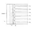
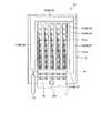
次に、タッチ検出機能付き表示装置1の構成例を詳細に説明する。図13は、タッチ検出機能付き表示装置を模式的に示す平面図である。図14は、タッチ検出機能付き表示装置の概略断面構造を表す断面図である。図15は、第1の実施形態に係るタッチ検出機能付き表示部の画素配列を表す回路図である。 Next, a configuration example of the display unit with a
図13に示すように、タッチ検出機能付き表示装置1は、画素基板2と、対向基板3と、カバー部材5とを含む。画素基板2と、対向基板3と、カバー部材5とは平面視で重畳して配置される。タッチ検出機能付き表示装置1は、さらに、ゲートドライバ12と、駆動電極ドライバ14と、表示制御用IC(図13では省略して示す)と、タッチ検出用IC18とを含む。画素基板2は、画像を表示させるための表示領域101aと、表示領域101aの外側の額縁領域101bとを有する。表示領域101aは、長辺と短辺とを有する矩形状である。額縁領域101bは、表示領域101aの4辺を囲む枠状となっている。本明細書において「額縁領域101b」とは、平面視でカバー部材5の外周よりも内側で、かつ、表示領域101aよりも外側の領域を示す。 As shown in FIG. 13, the
表示領域101aに、第1駆動電極COML1及びタッチ検出電極TDLが設けられている。額縁領域101bに第2駆動電極COML2A、COML2B、COML2C、COML2Dが設けられている。第1駆動電極COML1は、表示領域101aの長辺に沿った方向に延在するとともに、表示領域101aの短辺に沿った方向に複数配列されている。タッチ検出電極TDLは、表示領域101aの短辺に沿った方向に延在し、表示領域101aの長辺に沿った方向に複数配列されている。 The first drive electrode COML1 and the touch detection electrode TDL are provided in the
第2駆動電極COML2A、COML2B、COML2C、COML2Dは、それぞれ表示領域101aの外周の少なくともいずれか1辺に沿って配置されている。第2駆動電極COML2A、COML2B、COML2C、COML2Dは、表示領域101aの短辺若しくは長辺と同程度の長さ又はそれ以上の長さで配置されていることが好ましい。第2駆動電極COML2A、COML2B、COML2C、COML2Dは、表示領域101aの短辺若しくは長辺より短い長さであってもよい。第2駆動電極COML2A、COML2B、COML2C、COML2Dは、それぞれ表示領域101aの少なくとも1辺に沿った範囲内において電気的に分離されずに連続的につながっていることが好ましい。第1駆動電極COML1と第2駆動電極COML2A、COML2Bとは、互いに平行な方向に延在する。 The second drive electrodes COML2A, COML2B, COML2C, and COML2D are disposed along at least one side of the outer periphery of the
第2駆動電極COML2A、COML2B、COML2C、COML2Dは、額縁領域101bの各辺の端部に1本ずつ配置されている。1本の第2駆動電極COML2A、COML2B、COML2C、COML2Dは、それぞれカバー部材5の端まで配置されていることが好ましい。1本の第2駆動電極COML2A、COML2B、COML2C、COML2Dは、それぞれカバー部材5の端部と同一の箇所まで配置されていることが好ましい。第2駆動電極COML2A、COML2B、COML2C、COML2Dを金属で形成する場合に、腐食を防ぐなどの目的で保護膜を形成する場合など、第2駆動電極COML2A、COML2B、COML2C、COML2Dをカバー部材5の端まで形成できない場合、第2駆動電極COML2A、COML2B、COML2C、COML2Dがカバー部材5の端から10μmから100μmの範囲に形成されていることが好ましい。 The second drive electrodes COML2A, COML2B, COML2C, and COML2D are disposed one by one at the end of each side of the
このように、額縁領域101bの4辺のそれぞれの辺において表示領域101aの各辺以上の長さで延在するような1本の第2駆動電極COML2A、COML2B、COML2C、COML2Dがそれぞれ電気的に連続的に配置されることで、第2駆動電極COML2A、COML2B、COML2C、COML2Dと、表示領域101a内の電極との容量を利用して、額縁領域101bへの入力の有無を判別するボタン機能としてだけでなく、例えば表示領域101aの辺に沿った物体の一次元座標を取得することが可能となり、これらを表示領域101a内の検出結果と組み合わせてさまざまなアプリケーションへ反映させることができる。 In this manner, one second drive electrode COML2A, COML2B, COML2C, COML2D that electrically extends over a length of each side of the
額縁領域101bは表示領域101aと比較して非常に幅が狭いため、このような配置として額縁領域101bの1辺においてできるだけ大きな電極を配置することで額縁のタッチ検出の感度を向上させることができる。 Since the
本実施形態では、画素基板2上ではなく、カバー部材5に第2駆動電極COML2A、COML2B、COML2C、COML2Dを形成するので、カバー部材5の端部まで電極面積を確保することができる。第2駆動電極COML2A、COML2B、COML2C、COML2Dの幅は広ければ広いほどよい。しかし、第2駆動電極COML2A、COML2B、COML2C、COML2Dの幅は、第1駆動電極COML1の長さよりも細い。 In the present embodiment, since the second drive electrodes COML2A, COML2B, COML2C, and COML2D are formed not on the
図13に示すように、フレキシブル基板T1が画素基板2に接続されており、フレキシブル基板T2が対向基板3に接続されている。タッチ検出用IC18がフレキシブル基板T2に搭載されている。タッチ検出用IC18は、図1に示すタッチ検出部40が実装されており、タッチ検出電極TDLから出力される第1タッチ検出信号Vdet1が、フレキシブル基板T2を介してタッチ検出用IC18に供給される。 As shown in FIG. 13, the flexible substrate T <b> 1 is connected to the
図14に示すように、タッチ検出機能付き表示装置1は、画素基板2と、この画素基板2の表面に垂直な方向に対向して配置された対向基板3と、画素基板2と対向基板3との間に挿設された液晶層6と、対向基板3の画素基板2と反対側に配置されたカバー部材5とを備えている。 As shown in FIG. 14, the
画素基板2は、回路基板としてのTFT基板21と、このTFT基板21の上方にマトリックス状に配設された複数の画素電極22と、TFT基板21と画素電極22との間に設けられた複数の第1駆動電極COML1と、画素電極22と第1駆動電極COML1とを絶縁する絶縁層24と、を含む。TFT基板21の下側には、接着層を介して偏光板35Bが設けられていてもよい。 The
対向基板3は、ガラス基板31と、このガラス基板31の一方の面に形成されたカラーフィルタ32とを含む。ガラス基板31の他方の面には、タッチパネル30の検出電極であるタッチ検出電極TDLが設けられている。さらに、このタッチ検出電極TDLの上方には、偏光板35Aが設けられている。 The
カバー部材5は、カバー基材51と、着色層52と、第2駆動電極COML2A、COML2B、COML2C、COML2Dとを含む(図14では第2駆動電極COML2C、COML2Dは図示しない)。カバー基材51は、画素基板2及び対向基板3を覆って保護するための保護部材である。カバー基材51は、ガラス基板であってもよく、樹脂材料等を用いたフィルム状の基材であってもよい。カバー基材51の対向基板3と対向する面側に着色層52が設けられている。着色層52は、図13に示す額縁領域101bに設けられる。着色層52が設けられているため、ソースドライバ13、駆動電極ドライバ14等の回路や配線、フレキシブル基板T1、T2等が外部から視認されることを抑制することができる。着色層52は、例えば、光の透過を抑制するように着色された樹脂材料や、金属材料が用いられる。着色層52と重なる位置に、第2駆動電極COML2A、COML2Bが設けられている。図14では図示しない第2駆動電極COML2C、COML2Dも着色層52と重なる位置に設けられる。 The
TFT基板21とガラス基板31とは、図示しないスペーサを介して所定の間隔を設けて対向して配置される。TFT基板21とガラス基板31との間の空間に液晶層6が設けられる。液晶層6は、電界の状態に応じてそこを通過する光を変調するものであり、例えば、FFS(フリンジフィールドスイッチング)を含むIPS(インプレーンスイッチング)等の横電界モードの液晶が用いられる。なお、図14に示す液晶層6と画素基板2との間、及び液晶層6と対向基板3との間には、それぞれ配向膜が配設されてもよい。 The
TFT基板21には、図15に示す各副画素SPixの薄膜トランジスタ素子(以下、TFT素子)Tr、各画素電極22に画素信号Vpixを供給する画素信号線SGL、各TFT素子Trを駆動する駆動信号を供給する走査信号線GCL等の配線が形成されている。画素信号線SGL及び走査信号線GCLは、TFT基板21の表面と平行な平面に延在する。 The thin film transistor element (hereinafter referred to as TFT element) Tr of each subpixel SPix shown in FIG. 15, the pixel signal line SGL for supplying the pixel signal Vpix to each
図15に示す表示パネル20は、マトリックス状に配列された複数の副画素SPixを有している。副画素SPixは、それぞれTFT素子Tr及び液晶素子LCを備えている。TFT素子Trは、薄膜トランジスタにより構成されるものであり、この例では、nチャネルのMOS(Metal Oxide Semiconductor)型のTFTで構成されている。TFT素子Trのソースは画素信号線SGLに接続され、ゲートは走査信号線GCLに接続され、ドレインは液晶素子LCの一端に接続されている。液晶素子LCは、一端がTFT素子Trのドレインに接続され、他端が第1駆動電極COML1に接続されている。 The
副画素SPixは、走査信号線GCLにより、表示パネル20の同じ行に属する他の副画素SPixと互いに接続されている。走査信号線GCLは、ゲートドライバ12(図1参照)と接続され、ゲートドライバ12より走査信号Vscanが供給される。また、副画素SPixは、画素信号線SGLにより、表示パネル20の同じ列に属する他の副画素SPixと互いに接続されている。画素信号線SGLは、ソースドライバ13(図1参照)と接続され、ソースドライバ13より画素信号Vpixが供給される。さらに、副画素SPixは、第1駆動電極COML1により、同じ列に属する他の副画素SPixと互いに接続されている。第1駆動電極COML1は、駆動電極ドライバ14(図1参照)と接続され、駆動電極ドライバ14より第1駆動信号Vcomが供給される。つまり、この例では、同じ一列に属する複数の副画素SPixが一本の第1駆動電極COML1を共有するようになっている。本実施形態の第1駆動電極COML1は、画素信号線SGLの延出方向と平行に延び、走査信号線GCLの延出方向と交差する方向に延びる。第1駆動電極COML1は、これに限定されず、例えば走査信号線GCLと平行な方向に延びていてもよい。 The subpixels SPix are mutually connected to other subpixels SPix belonging to the same row of the
図1に示すゲートドライバ12は、走査信号線GCLを順次走査するように駆動する。ゲートドライバ12は、走査信号線GCLを介して、走査信号Vscan(図1参照)を副画素SPixのTFT素子Trのゲートに印加することにより、副画素SPixのうちの1行(1水平ライン)を表示駆動の対象として順次選択する。また、タッチ検出機能付き表示装置1は、1水平ラインに属する副画素SPixに対して、ソースドライバ13は、図15に示す画素信号線SGLを介して、画素信号Vpixを、選択された1水平ラインを構成する副画素SPixに供給する。そして、これらの副画素SPixでは、供給される画素信号Vpixに応じて1水平ラインずつ表示が行われるようになっている。この表示動作を行う際、駆動電極ドライバ14は、第1駆動電極COML1に対して第1駆動信号Vcomを印加する。画素電極22は、表示動作の第1駆動信号Vcomにより共通電位が供給される。 The
図14に示すカラーフィルタ32は、例えば赤(R)、緑(G)、青(B)の3色に着色されたカラーフィルタの色領域が周期的に配列されていてもよい。上述した図15に示す各副画素SPixに、R、G、Bの3色の色領域32R、32G、32Bが1組として対応付けられ、3色の色領域に対応する副画素SPixを1組として画素Pixが構成される。図14に示すように、カラーフィルタ32は、TFT基板21と垂直な方向において、液晶層6と対向する。なお、カラーフィルタ32は、異なる色に着色されていれば、他の色の組み合わせであってもよい。また、カラーフィルタ32は、3色の組み合わせに限定されず、4色以上の組み合わせであってもよい。 In the
図14及び図15に示す第1駆動電極COML1は、表示パネル20の複数の画素電極22に共通の電位を与える共通電極として機能するとともに、タッチパネル30の相互静電容量方式によるタッチ検出を行う際の駆動電極としても機能する。また、第1駆動電極COML1は、タッチパネル30の自己静電容量方式によるタッチ検出を行う際の検出電極として機能してもよい。図16は、第1の実施形態に係るタッチ検出機能付き表示部の駆動電極及びタッチ検出電極の一構成例を表す斜視図である。タッチパネル30は、画素基板2に設けられた第1駆動電極COML1と、対向基板3に設けられたタッチ検出電極TDLにより構成されている。 The first drive electrode COML1 shown in FIG. 14 and FIG. 15 functions as a common electrode for giving a common potential to the plurality of
第1駆動電極COML1は、図16の左右方向に延在する複数のストライプ状の電極パターンを含む。タッチ検出電極TDLは、第1駆動電極COML1の電極パターンの延在方向と交差する方向に延びる複数の電極パターンを含む。そして、タッチ検出電極TDLは、TFT基板21(図14参照)の表面に対する垂直な方向において、第1駆動電極COML1と対向している。タッチ検出電極TDLの各電極パターンは、タッチ検出部40のタッチ検出信号増幅部42の入力にそれぞれ接続される(図1参照)。第1駆動電極COML1の各電極パターンとタッチ検出電極TDLの各電極パターンとの交差部分に、それぞれ静電容量が形成される。 The first drive electrode COML1 includes a plurality of stripe-shaped electrode patterns extending in the left-right direction of FIG. The touch detection electrode TDL includes a plurality of electrode patterns extending in a direction intersecting the extending direction of the electrode pattern of the first drive electrode COML1. The touch detection electrode TDL is opposed to the first drive electrode COML1 in a direction perpendicular to the surface of the TFT substrate 21 (see FIG. 14). Each electrode pattern of the touch detection electrode TDL is connected to an input of the touch detection
タッチ検出電極TDL及び第1駆動電極COML1は、例えば、ITO(Indium Tin Oxide)等の透光性を有する導電性材料が用いられる。なお、タッチ検出電極TDL及び第1駆動電極COML1(駆動電極ブロック)は、ストライプ状に複数に分割される形状に限られない。例えば、タッチ検出電極TDL及び第1駆動電極COML1は、櫛歯形状等であってもよい。あるいはタッチ検出電極TDL及び第1駆動電極COML1は、複数に分割されていればよく、第1駆動電極COML1を分割するスリットの形状は直線であっても、曲線であってもよい。 For the touch detection electrode TDL and the first drive electrode COML1, for example, a conductive material having translucency such as ITO (Indium Tin Oxide) is used. The touch detection electrode TDL and the first drive electrode COML1 (drive electrode block) are not limited to the shape divided into a plurality of stripes. For example, the touch detection electrode TDL and the first drive electrode COML1 may have a comb shape or the like. Alternatively, the touch detection electrode TDL and the first drive electrode COML1 may be divided into a plurality, and the shape of the slit for dividing the first drive electrode COML1 may be a straight line or a curved line.
この構成により、タッチパネル30では、相互静電容量方式のタッチ検出動作を行う際、駆動電極ドライバ14が駆動電極ブロックとして時分割的に順次走査するように駆動することにより、第1駆動電極COML1の1検出ブロックが順次選択される。そして、タッチ検出電極TDLから第1タッチ検出信号Vdet1が出力されることにより、1検出ブロックのタッチ検出が行われるようになっている。つまり、駆動電極ブロックは、上述した相互静電容量方式のタッチ検出の基本原理における駆動電極E1に対応し、タッチ検出電極TDLは、タッチ検出電極E2に対応するものであり、タッチパネル30はこの基本原理に従ってタッチ入力を検出するようになっている。図16に示すように、タッチパネル30において、互いに交差したタッチ検出電極TDL及び第1駆動電極COML1は、静電容量式タッチセンサをマトリックス状に構成している。よって、タッチパネル30のタッチ検出面全体に亘って走査することにより、外部からの導体の接触又は近接が生じた位置の検出が可能となっている。 With this configuration, in the
次に図17から図19を参照して、第1駆動電極COML1、第2駆動電極COML2A、COML2B、COML2C、COML2D及びタッチ検出電極TDLの構成について説明する。図17は、第1の実施形態に係る画素基板を模式的に示す平面図である。図18は、第1の実施形態に係る対向基板を模式的に示す平面図である。図19は、第1の実施形態に係るカバー部材を模式的に示す平面図である。 Next, configurations of the first drive electrode COML1, the second drive electrodes COML2A, COML2B, COML2C, COML2D, and the touch detection electrode TDL will be described with reference to FIGS. 17 to 19. FIG. 17 is a plan view schematically showing a pixel substrate according to the first embodiment. FIG. 18 is a plan view schematically showing the counter substrate according to the first embodiment. FIG. 19 is a plan view schematically showing the cover member according to the first embodiment.
図17に示すように、第1駆動電極COML1は、TFT基板21の表示領域101aに設けられる。TFT基板21の額縁領域101bの短辺側に、駆動電極ドライバ14及び表示制御用IC19が配置され、額縁領域101bの長辺側にソースドライバ12が配置されている。表示制御用IC19は、TFT基板21にCOG(Chip On Glass)実装されたチップであり、上述した制御部11を内蔵したものである。表示制御用IC19は、外部のホストIC(図示しない)から供給された映像信号Vdisp(図1参照)に基づいて、走査信号線GCL及び画素信号線SGL等に制御信号を出力する。また、額縁領域101bの短辺側に、フレキシブル基板T1が接続されている。 As shown in FIG. 17, the first drive electrode COML1 is provided in the
本実施形態では、第1駆動電極COML1が走査信号線GCLの延在方向と交差する方向に延びている。このため、第1駆動電極COML1からの配線を額縁領域101bの短辺側(フレキシブル基板T1側)に引き出すことが可能である。したがって、第1駆動電極COML1を画素信号線SGLと直交する方向に設けた場合と比較して、額縁領域101bの長辺側に駆動電極ドライバ14を設ける必要がなく、額縁領域101bの幅を小さくすることができる。 In the present embodiment, the first drive electrode COML1 extends in a direction intersecting the extending direction of the scanning signal line GCL. For this reason, it is possible to lead the wiring from the first drive electrode COML1 to the short side (the flexible substrate T1 side) of the
また、駆動電極ドライバ14及びフレキシブル基板T1は、第1駆動電極COML1の延在方向の端部の近傍に配置されている。このため、第1駆動電極COML1から引き出される配線の長さを短くして、額縁領域101bの面積を小さくすることが可能である。 Further, the
図18に示すように、タッチ検出電極TDLは、ガラス基板31の表示領域101aに重なる領域に設けられる。ガラス基板31の額縁領域101bの短辺側にフレキシブル基板T2が接続される。タッチ検出電極TDLの端部から引き出された配線(図16では省略して示す)が額縁領域101bに設けられ、配線及びフレキシブル基板T2を介して、タッチ検出電極TDLとタッチ検出用IC18とが接続される。また、フレキシブル基板T2はコネクタ部TCを備えている。フレキシブル基板T2は、コネクタ部TCを介して後述するカバー部材5のフレキシブル基板T3と接続される。 As shown in FIG. 18, the touch detection electrodes TDL are provided in an area overlapping the
図19に示すように、カバー基材51の額縁領域101bに第2駆動電極COML2A、COML2B、COML2C、COML2Dが設けられている。カバー基材51の額縁領域101bの全面に着色層52が設けられており、第2駆動電極COML2A、COML2B、COML2C、COML2Dは着色層52と重なって配置される。なお、図19は、カバー部材5を上面側から見たときの平面図を示しており、模式的に第2駆動電極COML2A、COML2B、COML2C、COML2D等を示している。本明細書において「額縁領域101b」は、図17に斜線を付して示すように、平面視でカバー基材51の外周よりも内側であり、かつ表示領域101aの外側の領域である。 As shown in FIG. 19, the second drive electrodes COML2A, COML2B, COML2C, and COML2D are provided in the
第2駆動電極COML2A、COML2B、COML2C、COML2Dは、表示領域101aの4辺を囲むように設けられている。第2駆動電極COML2A、COML2Bは、それぞれ表示領域101aの長辺に沿った方向に連続して延在しており、表示領域101aを挟んで配置される。第2駆動電極COML2C、COML2Dは、表示領域101aの短辺に沿った方向に連続して延在しており、表示領域101aを挟んで配置される。 The second drive electrodes COML2A, COML2B, COML2C, and COML2D are provided so as to surround four sides of the
第2駆動電極COML2A、COML2B、COML2C、COML2Dは、互いに離隔しており、それぞれ配線54を介してフレキシブル基板T3と接続される。フレキシブル基板T3は、上述した対向基板3のフレキシブル基板T2にコネクタ部TCを介して接続される。これにより、タッチ検出用IC18と第2駆動電極COML2A、COML2B、COML2C、COML2Dとが接続される。タッチ検出用IC18に実装された駆動ドライバ48(図1参照)は、タッチ検出用の駆動信号を第2駆動電極COML2A、COML2B、COML2C、COML2Dに供給可能となっている。 The second drive electrodes COML2A, COML2B, COML2C, and COML2D are separated from each other, and are connected to the flexible substrate T3 through the
第2駆動電極COML2A、COML2B、COML2C、COML2D及び配線54は、銀(Ag)や銅(Cu)等の金属材料を含む導電性ペーストを用いて印刷法により形成することができる。また、第1駆動電極COML1と同様にITOを用いてもよい。第2駆動電極COML2A、COML2B、COML2C、COML2D及び配線54は、着色層52と重なる領域に設けられているため、導電性の高い金属材料を用いた場合であっても、外部から視認されることが抑制される。 The second drive electrodes COML2A, COML2B, COML2C, COML2D, and the
図20は、第2駆動電極とタッチ検出電極との関係を模式的に示す模式断面図である。図21は、第1駆動電極及び第2駆動電極の駆動方法を説明するための模式平面図である。図22は、第2駆動電極とタッチ検出電極との関係を拡大して模式的に示す模式平面図である。図20に示すように、第2駆動電極COML2A、COML2Bは、タッチ検出電極TDLの延在方向の端部よりも外側に配置され、かつ、タッチ検出電極TDLとは異なる層に配置されている。この場合であっても、第2駆動電極COML2A、COML2Bと、タッチ検出電極TDLとの間に静電容量が形成される。表示領域101aと額縁領域101bとの境界近傍又は額縁領域101bに、指が接触又は近接した場合、指によって形成される静電容量が、タッチ検出電極TDLの近傍にあることにより、第2駆動電極COML2A、COML2Bとタッチ検出電極TDLとの間にあるフリンジ分の静電容量が遮られる。このため、上述した相互静電容量方式のタッチ検出の基本原理に基づいて額縁領域101bへの指の接触又は接近を検出することができる。すなわち、額縁領域101bに配置された第2駆動電極COML2A、COML2Bから発生する駆動信号により電気力線が画面内に配置されたタッチ検出電極TDLに向かって延びることになる。額縁領域101bに指等の導電物が接触したり近づいたりすると、この電気力線が遮断されて面内に配置されたタッチ検出電極TDLの出力電位が低下することになる。 FIG. 20 is a schematic cross-sectional view schematically showing the relationship between the second drive electrode and the touch detection electrode. FIG. 21 is a schematic plan view for explaining a method of driving the first drive electrode and the second drive electrode. FIG. 22 is a schematic plan view schematically showing the relationship between the second drive electrode and the touch detection electrode in an enlarged manner. As shown in FIG. 20, the second drive electrodes COML2A and COML2B are disposed outside the end in the extending direction of the touch detection electrode TDL, and are disposed in a layer different from the touch detection electrode TDL. Even in this case, an electrostatic capacitance is formed between the second drive electrodes COML2A and COML2B and the touch detection electrode TDL. When the finger is in contact with or in proximity to the boundary between the
図21に示すように第2駆動電極COML2A、COML2Bは、タッチ検出用IC18に実装された駆動ドライバ48(図1参照)から第2駆動信号Vdが供給される。また、第1駆動電極COML1は、駆動電極ドライバ14から第1駆動信号Vcomが供給される。額縁領域101bに配置された第2駆動電極COML2A、COML2Bと、表示領域101aのタッチ検出電極TDLとの間の容量変化により額縁領域101bのタッチ検出が行われ、表示領域101aに配置されたタッチ検出電極TDLと第1駆動電極COML1との容量変化により表示領域101aのタッチ検出を行うので、第2駆動電極COML2A、COML2Bと、第1駆動電極COML1とを順次駆動した場合には、表示領域101aの外周付近のタッチ検出感度の低下を抑制することができる。 As shown in FIG. 21, the second drive signal COM is supplied from the drive driver 48 (see FIG. 1) mounted on the
第2駆動電極COML2A、COML2Bは、ガラス基板31の外縁よりも外側に配置されることが好ましい。こうすれば、ガラス基板31の額縁領域101bに設けられた配線等と、第2駆動電極COML2A、COML2Bとの間に形成される寄生容量を低減して、タッチ検出精度を向上させることができる。 The second drive electrodes COML2A and COML2B are preferably arranged outside the outer edge of the
図20に示すように、第2駆動電極COML2Aの端部55a及び第2駆動電極COML2Bの端部55bは、それぞれカバー基材51の端部57a、57bの近傍に配置されていることが好ましい。第2駆動電極COML2Aの端部55a及び第2駆動電極COML2Bの端部55bは、それぞれカバー基材51の端部57a、57bと重畳する位置に配置されていることがより好ましい。第2駆動電極COML2A、COML2Bを金属で形成する場合に、腐食を防ぐなどの目的で保護膜を形成する場合など、第2駆動電極COML2A、COML2Bをカバー基材51の端まで形成できない場合、第2駆動電極COML2Aの端部55aとカバー基材51の端部57aとの距離d1、及び第2駆動電極COML2Bの端部55bとカバー基材51の端部57bとの距離d2は、10μm以上、100μm以下の範囲であることが好ましい。 As shown in FIG. 20, the
図22に示すように、タッチ検出電極TDLの端部にパッド部38が設けられており、パッド部38から配線37が引き出されている。配線37は額縁領域101bを引き回され、フレキシブル基板T2(図18参照)に接続される。第2駆動電極COML2Aは、タッチ検出電極TDLの端部よりも外側に配置され、配線37の一部分と重畳していてもよい。つまり、第2駆動電極COML2Aは、タッチ検出電極TDLと重畳しない位置に設けられることが好ましい。なお、図22では図示しない第2駆動電極COML2Bについても同様に、配線37の一部分と重畳していてもよい。この場合、カバー基材51の額縁領域101bの幅を小さくすることができる。 As shown in FIG. 22, the
図23は、第1駆動電極と第2駆動電極との関係を模式的に示す模式断面図である。図24は、第1駆動電極と第2駆動電極との関係を模式的に示す模式断面図である。図23に示すように、第2駆動電極COML2C、COML2Dは、第1駆動電極COML1の延在方向の端部よりも外側に配置され、かつ、第1駆動電極COML1とは異なる層に配置されている。第2駆動電極COML2C、COML2Dと、第1駆動電極COML1との間に静電容量が形成される。本実施形態では、第2駆動電極COML2C、COML2Dと第1駆動電極COML1との間の容量変化により額縁領域101bのタッチ検出が行うことができる。この場合、第2駆動電極COML2C、COML2Dが上述した相互静電容量方式のタッチ検出の基本原理における駆動電極E1に対応し、第1駆動電極COML1が、タッチ検出電極E2に対応する。図22、図23に示すように、第2駆動電極COML2C、COML2Dに第2駆動信号Vdが供給される。また、第1駆動電極COML1にタッチ検出部40が接続されており、第1駆動電極COML1からタッチ検出部40を介して第1タッチ検出信号Vdet1が出力される。 FIG. 23 is a schematic cross-sectional view schematically showing the relationship between the first drive electrode and the second drive electrode. FIG. 24 is a schematic cross-sectional view schematically showing the relationship between the first drive electrode and the second drive electrode. As shown in FIG. 23, the second drive electrodes COML2C and COML2D are disposed outside the end in the extending direction of the first drive electrode COML1, and are disposed in a layer different from the first drive electrode COML1. There is. An electrostatic capacitance is formed between the second drive electrodes COML2C and COML2D and the first drive electrode COML1. In the present embodiment, the touch detection of the
図23に示すように、第2駆動電極COML2Cの端部55c及び第2駆動電極COML2Dの端部55dは、それぞれカバー基材51の端部57c、57dの近傍に配置されていることが好ましい。第2駆動電極COML2Cの端部55c及び第2駆動電極COML2Dの端部55dは、それぞれカバー基材51の端部57c、57dと重畳する位置に配置されていることがより好ましい。第2駆動電極COML2C、COML2Dを金属で形成する場合に、腐食を防ぐなどの目的で保護膜を形成する場合など、第2駆動電極COML2C、COML2Dをカバー基材51の端まで形成できない場合、第2駆動電極COML2Cの端部55cとカバー基材51の端部57cとの距離d3、及び第2駆動電極COML2Dの端部55dとカバー基材51の端部57dとの距離d4は、10μm以上、100μm以下の範囲であることが好ましい。 As shown in FIG. 23, the
本実施形態のタッチ検出機能付き表示装置1は、第2駆動電極COML2A、COML2B、COML2C、COML2Dが、カバー基材51の額縁領域101bに設けられているため、表示装置やタッチ検出装置の配線等の配置によらず額縁領域101bに電極面積の大きな額縁電極を連続的に配置することができる。In−CellやOn−Cellタッチパネルを備えた液晶表示装置ではガラス基板の額縁領域101bには配線やフレキシブル基板が配置されており、ここに額縁検出用の電極を配置するのは難しく、さらには近年では狭額縁等の要求があり液晶表示装置の額縁のみの配置では性能的に不十分である。カバー部材5側への配置はタッチ検出装置を含む電子機器のセット構造の最外周近くまで電極を配置することが可能であり、そのため、例えば額縁領域101bへ近接または接触した指の一次元座標を検出することができる。これにより、例えば額縁領域101bでのスライド操作やジェスチャ等を表示領域101aの表示動作やアプリケーションと連動させることが可能である。 In the
また、第2駆動電極COML2A、COML2B、COML2C、COML2Dを設けているため、表示領域101aと額縁領域101bとの境界近傍のタッチ検出感度を向上させることができる。したがって、タッチ検出面の全体のタッチ検出感度の均一性を向上させることができる。さらに、第2駆動電極COML2A、COML2B、COML2C、COML2Dを第1駆動電極COML1と異なる層に設けているため、第1駆動電極COML1をTFT基板21の額縁領域101bに設ける場合に比べ、TFT基板21の額縁領域101bの幅を小さくすることができる。したがって、本実施形態のタッチ検出機能付き表示装置1は、額縁領域の増大を抑制しつつ、優れた額縁検出性能を発揮することが可能である。 Further, since the second drive electrodes COML2A, COML2B, COML2C, and COML2D are provided, the touch detection sensitivity in the vicinity of the boundary between the
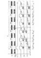
次に図25を参照して、本実施形態のタッチ検出機能付き表示装置1の駆動方法について説明する。図25は、第1の実施形態に係るタッチ検出機能付き表示装置の一動作例を示すタイミング波形図である。 Next, with reference to FIG. 25, a driving method of the display unit with a
タッチ検出機能付き表示装置1の動作方法の一例として、タッチ検出機能付き表示装置1は、タッチ検出動作(タッチ検出期間)と表示動作(表示動作期間)とを時分割に行う。タッチ検出動作と表示動作とはどのように分けて行ってもよいが、以下、表示パネル20の1フレーム期間(1F)、すなわち、1画面分の映像情報が表示されるのに要する時間の中において、タッチ検出動作と表示動作とをそれぞれ複数回に分割して行う方法について説明する。 As an example of the operation method of the
図25に示すように、制御信号(TS−VD)がONになると1フレーム期間(1F)が開始される。制御信号(TS−HD)は、1フレーム期間(1F)にONとOFFとが繰り返され、制御信号(TS−HD)がONの期間内にタッチ検出動作が実行され、OFFの期間内に表示動作が実行される。制御信号(TS−VD)及び制御信号(TS−HD)は、制御部11(図1参照)のクロック生成部のクロック信号に基づいて出力される。1フレーム期間(1F)は、複数の表示動作期間Pdx(x=1、2、…n)及びタッチ検出動作を行う複数のタッチ検出期間Ptx(x=1、2、…n)からなっている。これらの各期間は、時間軸上において、タッチ検出期間Pt1、表示動作期間Pd1、タッチ検出期間Pt2、表示動作期間Pd2、・・・のように交互に配置されている。As shown in FIG. 25, when the control signal (TS-VD) is turned on, one frame period (1F) is started. The control signal (TS-HD) is repeatedly turned on and off in one frame period (1F), the touch detection operation is executed within the period when the control signal (TS-HD) is on, and displayed within the period of off The action is performed. The control signal (TS-VD) and the control signal (TS-HD) are output based on the clock signal of the clock generation unit of the control unit 11 (see FIG. 1). One frame period (1F) includes a plurality of display operation periods Pdx (x = 1, 2,... N) and a plurality of touch detection periods Ptx (x = 1, 2,. ing. Each of these periods is alternately arranged on the time axis like a touch detection period Pt1 , a display operation period Pd1 , a touch detection period Pt2 , a display operation period Pd2 ,.
制御部11は、ゲートドライバ12とソースドライバ13とを介して、各表示動作期間Pdxに選択される複数行の画素Pix(図15参照)に画素信号Vpixを供給する。図25は、RGBの3色を選択する選択信号(SELR/G/B)及び色毎の映像信号(SIGn)を示している。選択信号(SELR/G/B)に従って、対応する各副画素SPixが選択され、色毎の映像信号(SIGn)が選択された副画素SPixに供給されることにより、画像の表示動作が実行される。それぞれの表示動作期間Pdxで、1画面分の映像信号Vdispをn分割した画像が表示され、表示動作期間Pd1、Pd2、…Pdnで1画面分の映像情報が表示される。The
タッチ検出期間Ptx(x=1、2、…n)の1回目のタッチ検出期間Pt1において、制御部11は、駆動ドライバ48に制御信号を出力する。駆動ドライバ48は、第2駆動電極COML2Aにタッチ検出用の第2駆動信号Vdを供給する。タッチ検出部40は、タッチ検出電極TDLから供給される第1タッチ検出信号Vdet1に基づいて、額縁領域101bに対するタッチ入力の有無および入力位置の座標の演算を行う。Touch detection periodPt x (x = 1,2, ... n) at first touch detection period Pt1, the
次に、タッチ検出期間Pt2、Pt3…において、制御部11は、駆動電極ドライバ14に制御信号を出力する。駆動電極ドライバ14は、第1駆動電極COML1にタッチ検出用の第1駆動信号Vcomを供給する。タッチ検出部40は、タッチ検出電極TDLから供給される第1タッチ検出信号Vdet1に基づいて、表示領域101aに対するタッチ入力の有無および入力位置の座標の演算を行う。Next, in the touch detection periods Pt2 , Pt3, ..., The
その後、タッチ検出期間Ptn−2では、第2駆動電極COML2Bに駆動ドライバ48から第2駆動信号Vdが供給され、タッチ検出電極TDLから第1タッチ検出信号Vdet1が出力される。タッチ検出期間Ptn−1に、第2駆動電極COML2Cに第2駆動信号Vdが供給され、第1駆動電極COML1から第1タッチ検出信号Vdet1が出力される。1フレーム期間(1F)の最後のタッチ検出期間Ptnにおいて、第2駆動電極COML2Dにタッチ検出用の第2駆動信号Vdが供給され、第1駆動電極COML1から第1タッチ検出信号Vdet1が出力される。タッチ検出部40は、タッチ検出電極TDL、第1駆動電極COML1から供給される第1タッチ検出信号Vdet1に基づいて、額縁領域101bに対するタッチ入力の有無および入力位置の座標の演算を行う。After that, in the touch detection period Ptn-2 , the second drive signal Vd is supplied from the
以上のように、1フレーム期間(1F)のタッチ検出期間Ptx(x=1、2、…n)において、制御部11は、駆動電極ドライバ14及び駆動ドライバ48に制御信号を出力して、第2駆動電極COML2A、COML2B、COML2C、COML2D及び第1駆動電極COML1の各検出ブロックに順次駆動信号が供給されるようにタッチ検出駆動走査を行う。それぞれのタッチ検出期間Ptxにおいて、タッチ検出電極TDLまたは第1駆動電極COML1からから第1タッチ検出信号Vdet1が出力される。このようなタッチ検出動作により、図17に示すTFT基板21の額縁領域101b及び図18に示すガラス基板31の額縁領域101bの面積の増大を抑制しつつ、タッチ検出可能な領域を表示領域101aの外側の額縁領域101bまで拡張して、額縁領域101bに対するタッチ入力を検出することができる。また、本実施形態のタッチ検出機能付き表示装置1は、第2駆動電極COML2A、第1駆動電極COML1の各検出ブロック、及び第2駆動電極COML2Bの順に駆動させることで、表示領域101aと額縁領域101bとの境界近傍のタッチ検出感度を向上させて、タッチ検出面の全体のタッチ検出感度の均一性を向上させることができる。As described above, in the touch detection period Ptx (x = 1, 2,... N) in one frame period (1F), the
本実施形態において、第1駆動電極COML1は表示パネル20の共通電極を兼用するので、制御部11は、表示動作期間Pdxにおいては、駆動電極ドライバ14を介して選択される第1駆動電極COML1に、表示駆動用の共通電位である第1駆動信号Vcomを供給する。In the present embodiment, since the first driving electrode COML1 is also serves as a common electrode of the
第2駆動電極COML2A、COML2B、COML2C、COML2Dの幅を大きくすることにより、接触又は近接する指などによる電界の変動の影響を受けやくなるため、タッチ検出感度が向上する。また、第2駆動電極COML2A、COML2B、COML2C、COML2Dの延在方向の長さは、第1駆動電極COML1よりも長くしてもよい。なお、本実施形態において、第2駆動電極COML2A、COML2B、COML2C、COML2Dの幅とは、表示領域101aの各辺と直交する方向の長さである。同様に第2駆動電極COML2A、COML2Bは、第1駆動電極COML1よりも大きい幅を有していることが好ましい。 By increasing the width of the second drive electrodes COML2A, COML2B, COML2C, and COML2D, the touch detection sensitivity is improved because the influence of the change in the electric field due to a finger touching or approaching is increased. In addition, the length in the extending direction of the second drive electrodes COML2A, COML2B, COML2C, and COML2D may be longer than that of the first drive electrode COML1. In the present embodiment, the width of the second drive electrodes COML2A, COML2B, COML2C, and COML2D is the length in the direction orthogonal to each side of the
なお、図25では、第2駆動信号Vdの振幅及び周波数は、第1駆動信号Vcomと同じ振幅及び周波数で示しているが、これに限られず、第1駆動信号Vcomと異なる振幅又は異なる周波数であってもよい。 Although the amplitude and frequency of the second drive signal Vd are shown in FIG. 25 with the same amplitude and frequency as the first drive signal Vcom, the present invention is not limited thereto. The amplitude and frequency are different from the first drive signal Vcom or different in frequency. It may be.
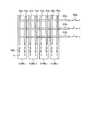
図26は、第1の実施形態の第1変形例に係るタッチ検出機能付き表示装置の一動作例を示すタイミング波形図である。図26は、第1駆動電極COML1及び第2駆動電極COML2A、COML2B、COML2C、COML2Dの駆動の順番は図25と同じであるが、第2駆動信号Vdの振幅が異なっている。第2駆動信号Vdの電位V7は第1駆動信号Vcomの電位V6よりも高くなっている。第2駆動電極COML2A、COML2B、COML2C、COML2Dは、映像表示に影響が少ないカバー基材51の額縁領域101bに設けられているため、TFT基板21に設けられた第1駆動電極COML1と比較すると制約なく所望の信号を供給することができる。そのため、第2駆動信号Vdの電位V7は第1駆動信号Vcomの電位V6よりも高くすることができ、額縁領域101bにおけるタッチ検出感度をさらに向上させることが可能である。額縁領域101bの検出に関しては、例えば電話のエッジ(ボリュームやオン、オフのスイッチ等)の検出を考えると、表示領域101aのタッチ検出電極TDLで検出する場合にはかなりの距離がある。額縁領域101bの検出感度を上げるためには、第2駆動電極COML2A、COML2B、COML2C、COML2Dの電界強度を上げると感度を大幅に上げることができる。FIG. 26 is a timing waveform chart showing an operation example of the display unit with a touch detection function according to the first modified example of the first embodiment. In FIG. 26, the driving order of the first drive electrode COML1 and the second drive electrodes COML2A, COML2B, COML2C, and COML2D is the same as that in FIG. 25, but the amplitude of the second drive signal Vd is different. The potentialV 7 of the second drive signal Vd is higher than the potentialV 6 of the first drive signal Vcom. Since the second drive electrodes COML2A, COML2B, COML2C, and COML2D are provided in the
また、第2駆動電極COML2A、COML2B、COML2C、COML2Dは、第1駆動電極COML1(図18では省略して示す)よりもカバー基材51側、つまり、接触又は近接する指等に近い位置に配置される。このため、駆動電極ドライバ14と異なる、タッチ検出用IC18に実装された駆動ドライバ48(図1参照)により駆動し、第1駆動信号Vcomと異なる振幅の第2駆動信号Vdで駆動することが好ましい。これにより、タッチ検出感度の均一性を向上させることが可能である。 In addition, the second drive electrodes COML2A, COML2B, COML2C, and COML2D are disposed at a position closer to the
図27は、第1の実施形態の第2変形例に係るタッチ検出機能付き表示装置の一動作例を示すタイミング波形図である。図27は、1フレーム期間(1F)において、表示領域101aのタッチ検出を行った後、額縁領域101bのタッチ検出を行う。すなわち、第1駆動電極COML1に対する第1駆動信号Vcomの供給が順次行われた後、タッチ検出期間Ptn−3からタッチ検出期間Ptnで、それぞれ第2駆動信号Vdが第2駆動電極COML2A、COML2B、COML2C、COML2Dに供給される。タッチ検出期間Ptn−3とタッチ検出期間Ptn−2ではタッチ検出電極TDLから第1タッチ検出信号Vdet1が出力される。タッチ検出期間Ptn−1とタッチ検出期間Ptnでは第1駆動電極COML1から第1タッチ検出信号Vdet1が出力される。このように額縁領域101bのタッチ検出期間を順次配置することにより、額縁領域101bのタッチ検出感度を向上させることができる。FIG. 27 is a timing waveform chart showing an operation example of the display unit with a touch detection function according to the second modified example of the first embodiment. In FIG. 27, after performing touch detection on the
図28は、第1の実施形態の第3変形例に係るタッチ検出機能付き表示装置の画素信号線及び走査信号線を模式的に示す平面図である。図23、図24で示すように、第1駆動電極COML1を検出電極として、第2駆動電極COML2C、COML2Dと第1駆動電極COML1との間の容量変化によりタッチ検出を行う。この場合、第1駆動電極COML1と第2駆動電極COML2C、COML2Dとの静電容量が大きくなり、第1駆動電極COML1から第1タッチ検出信号Vdet1が応答性良く出力されない場合がある。 FIG. 28 is a plan view schematically showing pixel signal lines and scanning signal lines of a display device with a touch detection function according to a third modified example of the first embodiment. As shown in FIGS. 23 and 24, touch detection is performed based on a change in capacitance between the second drive electrodes COML2C and COML2D and the first drive electrode COML1 using the first drive electrode COML1 as a detection electrode. In this case, the electrostatic capacitance between the first drive electrode COML1 and the second drive electrodes COML2C and COML2D may be large, and the first touch detection signal Vdet1 may not be output with good responsiveness from the first drive electrode COML1.
図28に示すように走査信号線GCLとゲートドライバ12とをそれぞれ接続する複数のスイッチSWgが設けられている。また、画素信号線SGLと第1駆動電極COML1とをそれぞれ接続する複数のスイッチSWsが設けられている。図25に示すタッチ検出期間Ptn−1、Ptnにおいて、スイッチSWg及びスイッチSWsをオフ状態にして、走査信号線GCL及び画素信号線SGLをフローティング状態とする。これにより、第1駆動電極COML1と走査信号線GCL及び第1駆動電極COML1と画素信号線SGLとの容量結合を抑制して検出感度の低下を低減できる。ここで、「フローティング状態」とは、固定された電位が与えられていない状態を示す。As shown in FIG. 28, a plurality of switches SWg for connecting the scanning signal line GCL and the
図29は、第1の実施形態の第4変形例に係るタッチ検出機能付き表示装置の画素信号線及び走査信号線を模式的に示す平面図である。第1駆動電極COML1を検出電極として用いる際に、スイッチSWgをオフ状態にして、走査信号線GCLをフローティング状態とする。そして、スイッチSWsをオン状態にして、画素信号線SGLと第1駆動電極COML1とを電気的に接続する。画素信号線SGLは、第1駆動電極COML1よりも導電性の高い金属材料が用いられているため、第1駆動電極COML1に画素信号線SGLを接続することで第1駆動電極COML1の見かけ上の抵抗値を低減することができる。これにより、検出感度の低下を抑制できる。 FIG. 29 is a plan view schematically showing pixel signal lines and scanning signal lines of a display device with a touch detection function according to a fourth modified example of the first embodiment. When the first drive electrode COML1 is used as a detection electrode, the switch SWg is turned off to set the scanning signal line GCL in a floating state. Then, the switch SWs is turned on to electrically connect the pixel signal line SGL and the first drive electrode COML1. Since the pixel signal line SGL is made of a metal material having higher conductivity than the first
(第2の実施形態)
図30は、第2の実施形態に係るタッチ検出機能付き表示装置を模式的に示す平面図である。第1の実施形態に係るタッチ検出機能付き表示装置は、図17に示すように、第1駆動電極COML1が表示領域101aの長辺に沿って延在しているがこれに限定されない。図30に示すように第2の実施形態のタッチ検出機能付き表示装置1Aは、TFT基板(図17参照)の表示領域101aに、複数の矩形状の第1駆動電極COML1Aが配置されている。複数の第1駆動電極COML1Aは、それぞれ互いに間隔を有してマトリクス状に配置される個別電極である。複数の第1駆動電極COML1Aのそれぞれから配線が引き出されており、配線を介して複数の第1駆動電極COML1Aと駆動電極ドライバ14とが接続されている。Second Embodiment
FIG. 30 is a plan view schematically showing the display device with a touch detection function according to the second embodiment. In the display device with a touch detection function according to the first embodiment, as shown in FIG. 17, the first drive electrode COML1 extends along the long side of the
なお、配線の配置は特に限定されず、第1駆動電極COML1Aと絶縁層を介して異なる層に設けてもよく、第1駆動電極COML1A同士の間に配置して第1駆動電極COML1Aと同一の層に設けてもよい。 The arrangement of the interconnections is not particularly limited, and may be provided in different layers via the first drive electrode COML1A and the insulating layer, and may be disposed between the first drive electrodes COML1A and identical to the first drive electrode COML1A. It may be provided in a layer.
表示領域101aのタッチ検出動作において、複数の第1駆動電極COML1Aに駆動電極ドライバ14から第1駆動信号Vcomが供給され、上述した自己静電容量方式のタッチ検出の基本原理に従って、第1駆動電極COML1Aから第2タッチ検出信号Vdet2が出力される。行列状に配置された第1駆動電極COML1Aのそれぞれについて、独立してタッチ検出を行うことにより、指などが接触又は近接したタッチパネル座標を検出することができる。 In the touch detection operation of the
図30に示すように、第2駆動電極COML2E、COML2Fがカバー部材5の額縁領域101bに設けられている。第2駆動電極COML2Eは、表示領域101aの長辺(左辺)に沿って延在する部分と、表示領域101aの短辺(上辺)に沿って延在する部分とが接続されている。第2駆動電極COML2Eは額縁領域101bの上辺から左辺にかけて連続して設けられる。第2駆動電極COML2Fは、表示領域101aの長辺(右辺)に沿って延在する部分と、表示領域101aの短辺(下辺)に沿って延在する部分とが接続されている。第2駆動電極COML2Fは額縁領域101bの左辺から下辺にかけて連続して設けられる。 As shown in FIG. 30, the second drive electrodes COML 2 E and COML 2 F are provided in the
カバー部材5の額縁領域101bに、フレキシブル基板T3が接続されている。第2駆動電極COML2E、COML2Fは、短い配線を介してフレキシブル基板T3と接続される。画素基板2のTFT基板21には、フレキシブル基板T1が接続されている。フレキシブル基板T1にタッチ検出用IC18Aが搭載されている。フレキシブル基板T3は、図示しないコネクタ部を介してフレキシブル基板T1と接続可能となっている。これにより、第2駆動電極COML2E、COML2Fは、タッチ検出用IC18Aに実装される駆動ドライバ48から第2駆動信号Vdが供給される。上述した相互静電容量方式のタッチ検出の基本原理に従って、第2駆動電極COML2E、COML2Fと第1駆動電極COML1Aとの容量変化により、第1駆動電極COML1Aから第1タッチ検出信号Vdet1が出力される。これにより、タッチ検出機能付き表示装置1Cは、額縁領域101bに接触又は近接する指などを検出することができる。 The flexible substrate T <b> 3 is connected to the
図31は、第2の実施形態に係るタッチ検出機能付き表示装置の一動作例を示すタイミング波形図である。図33に示すように、制御部11は、表示動作期間Pdにおいて、1フレーム分の画像について表示動作を実行する。表示動作において、第1駆動電極COML1Aは、表示パネル20の複数の画素電極22に共通の電位を与える共通電極として機能する。 FIG. 31 is a timing waveform chart showing an operation example of the display unit with a touch detection function according to the second embodiment. As shown in FIG. 33, the
表示動作期間Pdの後、制御部11は、タッチ検出期間Pt1、Pt3において相互静電容量方式によるタッチ検出動作を行い、タッチ検出期間Pt2において自己静電容量方式によるタッチ検出動作を行う。タッチ検出期間Pt1において、駆動ドライバ48は第2駆動電極COML2Eに第2駆動信号Vdを供給し、第1駆動電極COML1Aは第1タッチ検出信号Vdet1を出力する。タッチ検出期間Pt2において、駆動電極ドライバ14は、複数の第1駆動電極COML1Aに同時に第1駆動信号Vcomを供給し、複数の第1駆動電極COML1Aは第2タッチ検出信号Vdet2を出力する。タッチ検出期間Pt3において、駆動ドライバ48は第2駆動電極COML2Fに第2駆動信号Vdを供給し、第1駆動電極COML1Aは第1タッチ検出信号Vdet1を出力する。After the display operation period Pd, the
このようにして、1フレーム期間(1F)に表示領域101a及び額縁領域101bのタッチ検出動作が実行される。表示領域101aは自己静電容量方式によるタッチ検出が行われ、額縁領域101bは相互静電容量方式によるタッチ検出が行われる。このため、額縁領域101bでの検出精度を向上させることができる。本実施形態においても、第2駆動電極COML2E、COML2Fがカバー部材5に設けられているため、額縁領域101bの幅の増大を抑制しつつ、額縁領域101bにおけるタッチ検出を行うことができる。 In this manner, the touch detection operation of the
図32は、第2の実施形態に係る自己静電容量方式のタッチ検出の等価回路の一例を示す説明図である。図33は、第2の実施形態に係る自己静電容量方式のタッチ検出の駆動信号及びタッチ検出信号の波形の一例を表す図である。図32は、図11に示した等価回路に対して、電圧検出器DETがスイッチSW1、SW2を介さずに接続されている点が異なる。図32に示す電圧検出器DETは、反転入力部(−)に第1駆動電極COML1が接続され、非反転入力部(+)に第1駆動信号Vcomが入力される。図32の電圧検出器DETは、スイッチSW1、SW2は不要であり、直接、第1駆動信号Vcomが第1駆動電極COML1Aに供給される。 FIG. 32 is an explanatory diagram showing an example of an equivalent circuit of self-capacitance touch detection according to the second embodiment. FIG. 33 is a diagram illustrating an example of waveforms of a drive signal and a touch detection signal of a self-capacitance touch detection according to the second embodiment. FIG. 32 differs from the equivalent circuit shown in FIG. 11 in that the voltage detector DET is connected without passing through the switches SW1 and SW2. In the voltage detector DET illustrated in FIG. 32, the first drive electrode COML1 is connected to the inverting input unit (−), and the first driving signal Vcom is input to the non-inverting input unit (+). The voltage detector DET in FIG. 32 does not require the switches SW1 and SW2, and the first drive signal Vcom is directly supplied to the first drive electrode COML1A.
第1駆動電極COML1Aに指などの導体が近接又は接触して、第1駆動電極COML1Aの容量が増加すると、第1駆動信号Vcomとの差分の電圧に相当する電流が第1駆動電極COML1から出力側に流れる。電圧検出器DETは、この電流を電圧に変換し積分した値が出力される。スイッチSW3は、タッチ検出を行う際にオン(開)状態となり、タッチ検出を行わないときはオフ(閉)状態となり、電圧検出器DETのリセット動作を行う。また、電圧検出器DETは、相互静電容量方式のタッチ検出と、自己静電容量方式のタッチ検出とに兼用する場合、相互静電容量方式のタッチ検出の際に非反転入力部(+)に基準電圧Vrefが入力され、自己静電容量方式のタッチ検出の際に非反転入力部(+)に第1駆動信号Vcomが入力されるように切り替えられる。 When a conductor such as a finger approaches or contacts the first drive electrode COML1A and the capacitance of the first drive electrode COML1A increases, a current corresponding to a voltage difference with the first drive signal Vcom is output from the first drive electrode COML1 Flow to the side. The voltage detector DET converts this current into a voltage and outputs an integrated value. The switch SW3 is in the on (open) state when performing the touch detection, and is in the off (closed) state when the touch detection is not performed, and performs the reset operation of the voltage detector DET. In addition, when the voltage detector DET is used both for mutual capacitance touch detection and for self-capacitance touch detection, the non-inverting input unit (+) is used for mutual capacitance touch detection. The reference voltage Vref is input to the non-inverting input unit (+) so that the first drive signal Vcom is input at the time of self-capacitive touch detection.
図33に示すように、指が接触又は近接した場合の電圧の変動(点線の波形V8)は、指が接触又は近接していない場合の電圧の変動(実線の波形V9)と比べて振幅が大きくなる。これにより、波形V8と波形V9との電圧差分の絶対値|ΔV|は、指などの外部から接触又は近接する導体の影響に応じて変化することになる。このようにして、第1駆動電極COML1の自己静電容量に基づいてタッチ検出を行ってもよい。As shown in FIG. 33, the voltage fluctuation (waveform V8 in dotted line) when the finger is in contact or proximity is compared to the fluctuation in voltage (solid waveform V9 ) in the case where the finger is not in contact or proximity The amplitude increases. Thus, the absolute value of the voltage difference between the waveform V8 and the waveform V9 | ΔV | will vary depending on the influence of the conductor in contact with or close from the outside such as a finger. In this manner, touch detection may be performed based on the self-capacitance of the first drive electrode COML1.
なお、本実施形態は1フレーム分の表示動作を行う表示動作期間Pdの後にタッチ検出期間Pt1、Pt2、Pt3を配置しているが、表示動作期間とタッチ検出期間とを交互に複数回配置してもよい。この場合、タッチ検出期間を4回以上に分割して配置してもよい。本実施形態は、複数の第1駆動電極COML1Aによりタッチ検出動作を行うため、図12に示す対向基板3のタッチ検出電極TDLを設けなくてもよい。また、タッチ検出電極TDLを設けて、表示領域101aのタッチ検出動作において、相互静電容量方式のタッチ検出と自己静電容量方式のタッチ検出とを切り替えて実行してもよい。2本の第2駆動電極COML2E、COML2Fを設けているが、図13と同様に4本の第2駆動電極を設けてもよい。Although the touch detection periods Pt1 , Pt2 , and Pt3 are arranged after the display operation period Pd in which the display operation for one frame is performed in this embodiment, a plurality of display operation periods and touch detection periods are alternately arranged. It may be arranged once. In this case, the touch detection period may be divided into four or more times. In the present embodiment, since the touch detection operation is performed by the plurality of first drive electrodes COML1A, the touch detection electrodes TDL of the
次に、自己静電容量方式のタッチ検出動作における、寄生容量を低減する方法について説明する。図34は、第2の実施形態に係るタッチ検出機能付き表示装置の画素信号線及び走査信号線を模式的に示す平面図である。図35は、第2の実施形態に係るタッチ検出機能付き表示装置の一動作例を示すタイミング波形図である。 Next, a method of reducing parasitic capacitance in the self-capacitance touch detection operation will be described. FIG. 34 is a plan view schematically showing pixel signal lines and scanning signal lines of the display device with a touch detection function according to the second embodiment. FIG. 35 is a timing waveform chart showing an operation example of the display unit with a touch detection function according to the second embodiment.
第1駆動電極COML1Aは、走査信号線GCL及び画素信号線SGLに近接して配置されている。このため、第1駆動電極COML1Aと走査信号線GCLとの間の寄生容量及び第1駆動電極COML1Aと画素信号線SGLとの間の寄生容量が大きくなる。この寄生容量により、第1駆動電極COML1Aを応答性の良い波形で駆動することができない場合がある。また、寄生容量のバラツキによってタッチ検出信号の誤差が生じ、検出感度が低下する可能性がある。 The first drive electrode COML1A is disposed close to the scanning signal line GCL and the pixel signal line SGL. Therefore, the parasitic capacitance between the first drive electrode COML1A and the scanning signal line GCL and the parasitic capacitance between the first drive electrode COML1A and the pixel signal line SGL become large. There are cases where the first drive electrode COML1A can not be driven with a waveform with good responsiveness due to this parasitic capacitance. In addition, variations in parasitic capacitance may cause an error in the touch detection signal, which may lower the detection sensitivity.
図34に示すように走査信号線GCLとゲートドライバ12(図17参照)とをそれぞれ接続する複数のスイッチSWgが設けられている。また、画素信号線SGLとソースドライバ13とをそれぞれ接続する複数のスイッチSWsが設けられている。図35に示すタッチ検出期間Ptにおいて、走査信号線GCLと接続されたスイッチSWgをオフ状態にして、走査信号線GCLをフローティング状態とする。また、タッチ検出期間Ptにおいて、画素信号線SGLと接続されたスイッチSWsをオン状態にする。図35に示すように、画素信号線SGLは、第1駆動信号Vcomと同期した同一の波形の信号Vsglが入力される。これによって、第1駆動電極COML1Aと画素信号線SGLとの間の寄生容量を低減して、第1駆動電極COML1Aを所望の波形で駆動することができる。 As shown in FIG. 34, a plurality of switches SWg are provided for connecting the scanning signal line GCL and the gate driver 12 (see FIG. 17). In addition, a plurality of switches SWs which respectively connect the pixel signal line SGL and the
なお、第1駆動信号Vcomと同期した信号Vsglが入力される画素信号線SGLは、第1駆動電極COML1Aと電気的に接続して駆動したほうが好ましい。第1駆動電極COML1Aは、ITO等の透光性を有する導電性材料が用いられるため、金属材料で形成される画素信号線SGLよりも抵抗が高い。画素信号線SGLと第1駆動電極COML1Aとを電気的に接続して駆動することで、画素信号線SGLと第1駆動電極COML1Aとの合計の抵抗値が低減されるため、消費電力等のメリットがある。信号Vsglは、第1駆動信号Vcomが入力された第1駆動電極COML1Aに対応していない画素信号線SGLに対して入力してもよい。なお、信号Vsglは、第1駆動信号Vcom又は第2駆動信号Vdと同期した同一の波形であることが好ましいが、第1駆動信号Vcom又は第2駆動信号Vdと異なる振幅を有して高レベルの電位と低レベルの電位とがシフトする波形であってもよい。 The pixel signal line SGL to which the signal Vsgl synchronized with the first drive signal Vcom is input is preferably electrically connected to the first drive electrode COML1A and driven. The first drive electrode COML1A uses a light-transmitting conductive material such as ITO, and thus has a higher resistance than the pixel signal line SGL formed of a metal material. By electrically connecting and driving the pixel signal line SGL and the first drive electrode COML1A, the total resistance value of the pixel signal line SGL and the first drive electrode COML1A is reduced, so that merits such as power consumption can be obtained. There is. The signal Vsgl may be input to the pixel signal line SGL which does not correspond to the first drive electrode COML1A to which the first drive signal Vcom is input. The signal Vsgl preferably has the same waveform synchronized with the first drive signal Vcom or the second drive signal Vd, but has a different amplitude from that of the first drive signal Vcom or the second drive signal Vd and has a high level. It may be a waveform in which the potential of V and the potential of low level shift.
次に、図36及び図37を参照して、自己静電容量方式のタッチ検出動作における、寄生容量を低減する他の方法について説明する。図36は、第2の実施形態の変形例に係るタッチ検出機能付き表示装置の画素信号線及び走査信号線を模式的に示す平面図である。図37は、第2の実施形態の変形例に係るタッチ検出機能付き表示装置の一動作例を示すタイミング波形図である。 Next, with reference to FIGS. 36 and 37, another method of reducing parasitic capacitance in the self-capacitance touch detection operation will be described. FIG. 36 is a plan view schematically showing pixel signal lines and scanning signal lines of a display device with a touch detection function according to a modification of the second embodiment. FIG. 37 is a timing waveform chart showing an operation example of the display unit with a touch detection function according to a modification of the second embodiment.
タッチ検出期間Ptにおいて、走査信号線GCLと接続されたスイッチSWgをオン状態にして、画素信号線SGLと接続されたスイッチSWsをオン状態にする。すなわち、走査信号線GCL及び画素信号線SGLをフローティング状態にしない。そして、図37に示すように、走査信号線GCL及び画素信号線SGLに、第1駆動信号Vcomと同期した同一の波形の信号Vgcl、Vsglが入力される。これによって、第1駆動電極COML1Aと走査信号線GCLとの間の寄生容量が低減され、かつ、第1駆動電極COML1Aと画素信号線SGLとの間の寄生容量が低減される。したがって、第1駆動電極COML1Aを所望の波形で駆動することができる。なお、走査信号線GCLに供給される信号Vgclは、図15に示すTFT素子Trがオフ状態を維持できるような電圧の波形とする。これは、副画素SPixごとに設置されているTFT素子がオン状態となってリークが発生して、表示画質が悪化することを防止するためである。 In the touch detection period Pt, the switch SWg connected to the scanning signal line GCL is turned on, and the switch SWs connected to the pixel signal line SGL is turned on. That is, the scanning signal line GCL and the pixel signal line SGL are not brought into the floating state. Then, as shown in FIG. 37, the signals Vgcl and Vsgl of the same waveform synchronized with the first drive signal Vcom are input to the scanning signal line GCL and the pixel signal line SGL. Thereby, the parasitic capacitance between the first drive electrode COML1A and the scanning signal line GCL is reduced, and the parasitic capacitance between the first drive electrode COML1A and the pixel signal line SGL is reduced. Therefore, the first drive electrode COML1A can be driven with a desired waveform. Note that the signal Vgcl supplied to the scanning signal line GCL has a waveform of a voltage that allows the TFT element Tr shown in FIG. 15 to maintain the off state. This is to prevent the display image quality from being deteriorated due to the TFT element provided for each sub-pixel SPix being turned on to cause a leak.
以上、本発明の好適な実施の形態を説明したが、本発明はこのような実施の形態に限定されるものではない。実施の形態で開示された内容はあくまで一例にすぎず、本発明の趣旨を逸脱しない範囲で種々の変更が可能である。本発明の趣旨を逸脱しない範囲で行われた適宜の変更についても、当然に本発明の技術的範囲に属する。 As mentioned above, although the preferred embodiment of the present invention was described, the present invention is not limited to such an embodiment. The content disclosed in the embodiment is merely an example, and various modifications can be made without departing from the scope of the present invention. Appropriate modifications made without departing from the spirit of the present invention also of course fall within the technical scope of the present invention.
例えば、第1駆動電極が表示パネルの共通電極を兼用する場合を説明したが、これに限られない。表示パネルに共通電極を設け、この表示パネルの上にタッチパネルを装着したタッチ検出機能付き表示装置であってもよい。また、カバー基材に設けられた第2駆動電極の形状や、配置、個数等は適宜変更してもよい。例えば、第2駆動電極は表示領域の4辺を囲むように設けられているが、4辺のうちいずれかの辺に第2駆動電極が設けられていない場合であってもよい。 For example, although the case where the first drive electrode doubles as the common electrode of the display panel has been described, the present invention is not limited thereto. The display device may be a display device with a touch detection function in which a common electrode is provided on the display panel and a touch panel is mounted on the display panel. In addition, the shape, arrangement, number, etc. of the second drive electrodes provided on the cover substrate may be changed as appropriate. For example, although the second drive electrodes are provided to surround four sides of the display area, the second drive electrodes may not be provided on any of the four sides.
1、1A タッチ検出機能付き表示装置
2 画素基板
3 対向基板
5 カバー部材
6 液晶層
10 タッチ検出機能付き表示部
11 制御部
12 ゲートドライバ
13 ソースドライバ
14 駆動電極ドライバ
20 表示パネル
21 TFT基板
22 画素電極
30 タッチパネル
31 ガラス基板
32 カラーフィルタ
40 タッチ検出部
42 タッチ検出信号増幅部
43 A/D変換部
44 信号処理部
45 座標抽出部
46 検出タイミング制御部
48 駆動ドライバ
51 カバー基材
52 着色層
101a 表示領域
101b 額縁領域
COML1、COML1A 第1駆動電極
COML2A、COML2B、COML2C、COML2D、COML2E、COML2F 第2駆動電極
GCL 走査信号線
Pd 表示動作期間
Pt タッチ検出期間
Pix 画素
SPix 副画素
SGL 画素信号線
TDL タッチ検出電極
Vcom 第1駆動信号
Vd 第2駆動信号
Vdet1 第1タッチ検出信号
Vdet2 第2タッチ検出信号
Vdisp 映像信号
Vpix 画素信号
Vscan 走査信号DESCRIPTION OF
Claims (14)
Translated fromJapanese前記第1基板と対向する第2基板と、
前記第2基板と対向するカバー基材と、
前記第1基板と平行な面上の表示領域に重畳して配置される複数の第1電極と、
前記カバー基材上の、前記表示領域の外側の額縁領域と重畳する場所に配置される少なくとも1つの第2電極と、
前記表示領域において、いずれかの前記第2電極と平行な方向に延在する複数の第3電極と、
第1駆動信号を前記第3電極に出力する第1駆動部と、
第2駆動信号を前記第2電極に出力する第2駆動部と、を有し、
前記第1電極と前記第2電極との静電容量に基づいて前記額縁領域への物体の近接または接触が感知され、
前記第2電極は、前記額縁領域のいずれかの辺に沿って延在し、
前記第2駆動信号の電位が前記第1駆動信号の電位より高い、タッチ検出装置。A first substrate,
A second substrate facing the first substrate;
A cover substrate facing the second substrate;
A plurality of first electrodes disposed to overlap a display area on a surface parallel to the first substrate;
At least one second electrode disposed on the cover substrate at a position overlapping the frame area outside the display area;
A plurality of third electrodes extending in a direction parallel to any one of the second electrodes in the display area;
A first drive unit that outputs a first drive signal to the third electrode;
And a second drive unit that outputs a second drive signal to the second electrode ,
Proximity or contact of an object to the frame area is sensed based on the capacitance of the first electrode and the second electrode;
The second electrode mayextend along either side of the frameregion,
The touch detection device, wherein the potential of the second drive signal is higher than the potential of the first drive signal .
前記第1電極は、少なくともいずれかの前記第2電極が延在する方向に対して交差する方向に延在し、かつ前記第2電極が延在する方向に対して平行な方向に配列し、前記表示領域の端部において前記第2電極との間に容量を形成する、請求項1または請求項2に記載のタッチ検出装置。The plurality of first electrodes are detection electrodes, and the at least one second electrode is a drive electrode,
The first electrode extends in a direction intersecting with a direction in which at least one of the second electrodes extends, and is arranged in a direction parallel to a direction in which the second electrode extends, The touch detection device according to claim 1, wherein a capacitance is formed between the end of the display area and the second electrode.
前記第1基板と平行な面上の前記表示領域において、行列配置された複数の画素電極と、
前記表示領域内において画像表示機能を発揮する表示機能層と、を有するタッチ検出機能付き表示装置。And the touch detection device according to any one of claims 10 to claim 1,
A plurality of pixel electrodes arranged in a matrix in the display area on a plane parallel to the first substrate;
A display device with a touch detection function, comprising: a display functional layer that exhibits an image display function in the display area.
前記タッチ検出動作の期間中に、前記画素信号線および前記走査信号線の電位がフローティングである、請求項12に記載のタッチ検出機能付き表示装置。The first substrate is provided with a plurality of pixel signal lines and a plurality of scanning signal lines which are disposed to intersect with each other in plan view.
During the touch detection operation, the potential of the pixel signal lines and the scanning signal line is in a floating display device with a touch detection function according to claim 12.
前記第1基板と平行な面上の前記表示領域において、行列配置された複数の画素電極と、
前記表示領域内において画像表示機能を発揮する表示機能層と、を有し
前記第1基板は、互いに平面視で交差して配設された複数の画素信号線及び複数の走査信号線が設けられており、
物体の近接または接触を検出するタッチ検出動作の期間中に、前記走査信号線の電位がフローティングであって、前記画素信号線の電位は、前記第1駆動信号または前記第2駆動信号と同期してシフトするタッチ検出機能付き表示装置。A touch detection device according to claim1 ;
A plurality of pixel electrodes arranged in a matrix in the display area on a plane parallel to the first substrate;
The first substrate is provided with a plurality of pixel signal lines and a plurality of scanning signal lines disposed so as to intersect with each other in plan view. Yes,
During the touch detection operation for detecting proximity or contact of an object, the potential of the scanning signal line is floating, and the potential of the pixel signal line is synchronized with the first drive signal or the second drive signal. Display device with touch detection function to shift.
Priority Applications (7)
| Application Number | Priority Date | Filing Date | Title |
|---|---|---|---|
| JP2015232252AJP6549976B2 (en) | 2015-11-27 | 2015-11-27 | Touch detection device and display device with touch detection function |
| US15/346,093US10126863B2 (en) | 2015-11-27 | 2016-11-08 | Touch detection device, display device with touch detection function, and covering member |
| CN201611042297.3ACN107037911B (en) | 2015-11-27 | 2016-11-23 | Touch detection device, display device with touch detection function, and cover member |
| US16/163,819US10551962B2 (en) | 2015-11-27 | 2018-10-18 | Touch detection device, display device with touch detection function, and covering member |
| US16/682,220US11086429B2 (en) | 2015-11-27 | 2019-11-13 | Touch detection device, display device with touch detection function, and covering member |
| US17/376,917US11687178B2 (en) | 2015-11-27 | 2021-07-15 | Touch detection device, display device with touch detection function, and covering member |
| US18/196,117US12056303B2 (en) | 2015-11-27 | 2023-05-11 | Touch detection device, display device with touch detection function, and covering member |
Applications Claiming Priority (1)
| Application Number | Priority Date | Filing Date | Title |
|---|---|---|---|
| JP2015232252AJP6549976B2 (en) | 2015-11-27 | 2015-11-27 | Touch detection device and display device with touch detection function |
Publications (2)
| Publication Number | Publication Date |
|---|---|
| JP2017097794A JP2017097794A (en) | 2017-06-01 |
| JP6549976B2true JP6549976B2 (en) | 2019-07-24 |
Family
ID=58776919
Family Applications (1)
| Application Number | Title | Priority Date | Filing Date |
|---|---|---|---|
| JP2015232252AActiveJP6549976B2 (en) | 2015-11-27 | 2015-11-27 | Touch detection device and display device with touch detection function |
Country Status (3)
| Country | Link |
|---|---|
| US (5) | US10126863B2 (en) |
| JP (1) | JP6549976B2 (en) |
| CN (1) | CN107037911B (en) |
Families Citing this family (22)
| Publication number | Priority date | Publication date | Assignee | Title |
|---|---|---|---|---|
| JP6549976B2 (en)* | 2015-11-27 | 2019-07-24 | 株式会社ジャパンディスプレイ | Touch detection device and display device with touch detection function |
| US10754465B2 (en)* | 2017-02-15 | 2020-08-25 | Sharp Kabushiki Kaisha | Display device |
| TWI622912B (en)* | 2017-03-08 | 2018-05-01 | 宏碁股份有限公司 | Electronic device with touch function and operation method thereof |
| US10572087B2 (en)* | 2017-07-27 | 2020-02-25 | Cirque Corporation | Self-capacitence sensor and sensor array sensitivity calibration method using secondary mutual capacitence measurements |
| CN109388263B (en)* | 2017-08-04 | 2022-01-18 | 鸿富锦精密工业(深圳)有限公司 | Touch control display device |
| GB2568217A (en) | 2017-08-08 | 2019-05-15 | Cambridge Touch Tech Ltd | Touch panel pressure detection |
| JP7028886B2 (en)* | 2017-11-10 | 2022-03-02 | アルプスアルパイン株式会社 | Input device |
| KR102419066B1 (en)* | 2017-11-20 | 2022-07-08 | 엘지디스플레이 주식회사 | Touch display panel and touch display device |
| KR102562900B1 (en)* | 2018-02-02 | 2023-08-04 | 삼성디스플레이 주식회사 | Flexible display apparatus and touch sensitive display apparatus |
| WO2019165577A1 (en)* | 2018-02-27 | 2019-09-06 | 深圳市汇顶科技股份有限公司 | Sensor and touch display screen |
| JP6878678B2 (en)* | 2018-03-05 | 2021-06-02 | 株式会社ジャパンディスプレイ | Touch sensor that corrects hover detection value |
| JP2019160174A (en)* | 2018-03-16 | 2019-09-19 | シャープ株式会社 | Liquid crystal display panel |
| US10976876B2 (en)* | 2018-06-18 | 2021-04-13 | Synaptics Incorporated | Conductive guides for proximity sensing devices |
| CN108768373A (en)* | 2018-07-03 | 2018-11-06 | 珠海进田电子科技有限公司 | A kind of novel line control machine of gesture control |
| CN109814758B (en)* | 2019-01-30 | 2021-05-18 | 合肥鑫晟光电科技有限公司 | Touch substrate, touch driving method and electronic device |
| GB2581495A (en) | 2019-02-19 | 2020-08-26 | Cambridge Touch Tech Ltd | Force sensing touch panel |
| GB2582171B (en) | 2019-03-13 | 2022-10-12 | Cambridge Touch Tech Ltd | Force sensing touch panel |
| US11397487B2 (en)* | 2020-03-17 | 2022-07-26 | Synaptics Incorporated | Re-configurable receiver channels for a sensing device |
| TWI749596B (en)* | 2020-06-17 | 2021-12-11 | 禾瑞亞科技股份有限公司 | Touch sensitive processing method and apparatus and touch system |
| TWI749968B (en)* | 2020-06-17 | 2021-12-11 | 禾瑞亞科技股份有限公司 | Touch sensitive processing apparatus and method thereof, touch system and touch panel |
| JP7565180B2 (en)* | 2020-09-18 | 2024-10-10 | 株式会社ジャパンディスプレイ | Display device and sterilizer |
| CN112732114A (en)* | 2020-12-29 | 2021-04-30 | 天马微电子股份有限公司 | Touch panel, driving method of touch panel and display device |
Family Cites Families (18)
| Publication number | Priority date | Publication date | Assignee | Title |
|---|---|---|---|---|
| US7656393B2 (en)* | 2005-03-04 | 2010-02-02 | Apple Inc. | Electronic device having display and surrounding touch sensitive bezel for user interface and control |
| JP4816668B2 (en) | 2008-03-28 | 2011-11-16 | ソニー株式会社 | Display device with touch sensor |
| US9335868B2 (en) | 2008-07-31 | 2016-05-10 | Apple Inc. | Capacitive sensor behind black mask |
| JP5510451B2 (en)* | 2009-04-28 | 2014-06-04 | 日本電気株式会社 | Touch panel, touch panel manufacturing method, and electronic device |
| JP2011198009A (en)* | 2010-03-19 | 2011-10-06 | Sony Corp | Electro-optical device with input function |
| CN102576276B (en)* | 2010-08-23 | 2017-05-10 | 谱瑞科技股份有限公司 | Capacitive Scan Proximity Detection |
| JP2012133453A (en) | 2010-12-20 | 2012-07-12 | Sony Corp | Information processing device, information processing method and program |
| US8804056B2 (en)* | 2010-12-22 | 2014-08-12 | Apple Inc. | Integrated touch screens |
| KR101474061B1 (en)* | 2012-05-04 | 2014-12-17 | 엘지디스플레이 주식회사 | Sensor for detecting proximity/motion and touch and display device having the same |
| JP5778122B2 (en) | 2012-12-14 | 2015-09-16 | 株式会社ジャパンディスプレイ | Display device with touch detection function and electronic device including the same |
| JP2014174760A (en)* | 2013-03-08 | 2014-09-22 | Japan Display Inc | Display device attached with touch detection function, and electronic device |
| US9626048B2 (en)* | 2014-01-13 | 2017-04-18 | Himax Technologies Limited | Touch screen and related touch sensing control circuit |
| JP6375223B2 (en)* | 2014-01-31 | 2018-08-15 | 株式会社ジャパンディスプレイ | Display device with sensor and driving method thereof |
| JP2017107253A (en)* | 2014-04-14 | 2017-06-15 | シャープ株式会社 | Display device and electronic device |
| US10139869B2 (en)* | 2014-07-23 | 2018-11-27 | Analog Devices, Inc. | Capacitive sensors for grip sensing and finger tracking |
| WO2016056516A1 (en)* | 2014-10-10 | 2016-04-14 | シャープ株式会社 | Display device |
| CN104597646B (en)* | 2014-12-22 | 2018-09-07 | 上海天马微电子有限公司 | Display panel and display device |
| JP6549976B2 (en)* | 2015-11-27 | 2019-07-24 | 株式会社ジャパンディスプレイ | Touch detection device and display device with touch detection function |
- 2015
- 2015-11-27JPJP2015232252Apatent/JP6549976B2/enactiveActive
- 2016
- 2016-11-08USUS15/346,093patent/US10126863B2/enactiveActive
- 2016-11-23CNCN201611042297.3Apatent/CN107037911B/enactiveActive
- 2018
- 2018-10-18USUS16/163,819patent/US10551962B2/enactiveActive
- 2019
- 2019-11-13USUS16/682,220patent/US11086429B2/enactiveActive
- 2021
- 2021-07-15USUS17/376,917patent/US11687178B2/enactiveActive
- 2023
- 2023-05-11USUS18/196,117patent/US12056303B2/enactiveActive
Also Published As
| Publication number | Publication date |
|---|---|
| US12056303B2 (en) | 2024-08-06 |
| JP2017097794A (en) | 2017-06-01 |
| US20200081574A1 (en) | 2020-03-12 |
| US11687178B2 (en) | 2023-06-27 |
| US20210342028A1 (en) | 2021-11-04 |
| US10551962B2 (en) | 2020-02-04 |
| CN107037911B (en) | 2020-06-02 |
| US11086429B2 (en) | 2021-08-10 |
| US20170153749A1 (en) | 2017-06-01 |
| US20230289003A1 (en) | 2023-09-14 |
| CN107037911A (en) | 2017-08-11 |
| US20190050107A1 (en) | 2019-02-14 |
| US10126863B2 (en) | 2018-11-13 |
Similar Documents
| Publication | Publication Date | Title |
|---|---|---|
| JP6549976B2 (en) | Touch detection device and display device with touch detection function | |
| US10817100B2 (en) | Detection device, display device, and electronic apparatus | |
| JP6375223B2 (en) | Display device with sensor and driving method thereof | |
| CN105278782B (en) | The display device and its driving method of belt sensor | |
| JP5909201B2 (en) | Touch detection device, display device with touch detection function and electronic device including the same | |
| JP6677545B2 (en) | Display device | |
| CN107179848B (en) | Detection device, display device and electronic equipment | |
| JP2017228162A (en) | Array substrate, display device, and sensor electrode inspection method | |
| JP6030453B2 (en) | Touch detection device, display device with touch detection function and electronic device including the same | |
| JP7189996B2 (en) | detector | |
| JP2018169680A (en) | Display device | |
| JP2018190347A (en) | Display device | |
| JP7221618B2 (en) | Display device | |
| KR20150118861A (en) | Touch detecting apparatus |
Legal Events
| Date | Code | Title | Description |
|---|---|---|---|
| A621 | Written request for application examination | Free format text:JAPANESE INTERMEDIATE CODE: A621 Effective date:20180829 | |
| A977 | Report on retrieval | Free format text:JAPANESE INTERMEDIATE CODE: A971007 Effective date:20190313 | |
| A131 | Notification of reasons for refusal | Free format text:JAPANESE INTERMEDIATE CODE: A131 Effective date:20190402 | |
| A521 | Request for written amendment filed | Free format text:JAPANESE INTERMEDIATE CODE: A523 Effective date:20190522 | |
| TRDD | Decision of grant or rejection written | ||
| A01 | Written decision to grant a patent or to grant a registration (utility model) | Free format text:JAPANESE INTERMEDIATE CODE: A01 Effective date:20190611 | |
| A61 | First payment of annual fees (during grant procedure) | Free format text:JAPANESE INTERMEDIATE CODE: A61 Effective date:20190628 | |
| R150 | Certificate of patent or registration of utility model | Ref document number:6549976 Country of ref document:JP Free format text:JAPANESE INTERMEDIATE CODE: R150 | |
| R250 | Receipt of annual fees | Free format text:JAPANESE INTERMEDIATE CODE: R250 | |
| R250 | Receipt of annual fees | Free format text:JAPANESE INTERMEDIATE CODE: R250 | |
| R250 | Receipt of annual fees | Free format text:JAPANESE INTERMEDIATE CODE: R250 | |
| R250 | Receipt of annual fees | Free format text:JAPANESE INTERMEDIATE CODE: R250 | |
| S111 | Request for change of ownership or part of ownership | Free format text:JAPANESE INTERMEDIATE CODE: R313113 | |
| R350 | Written notification of registration of transfer | Free format text:JAPANESE INTERMEDIATE CODE: R350 |