JP6549355B2 - Fluid handling device - Google Patents
Fluid handling deviceDownload PDFInfo
- Publication number
- JP6549355B2 JP6549355B2JP2014123551AJP2014123551AJP6549355B2JP 6549355 B2JP6549355 B2JP 6549355B2JP 2014123551 AJP2014123551 AJP 2014123551AJP 2014123551 AJP2014123551 AJP 2014123551AJP 6549355 B2JP6549355 B2JP 6549355B2
- Authority
- JP
- Japan
- Prior art keywords
- film
- region
- substrate
- transfer layer
- hole
- Prior art date
- Legal status (The legal status is an assumption and is not a legal conclusion. Google has not performed a legal analysis and makes no representation as to the accuracy of the status listed.)
- Expired - Fee Related
Links
- 239000012530fluidSubstances0.000titleclaimsdescription18
- 239000010408filmSubstances0.000claimsdescription89
- 238000012546transferMethods0.000claimsdescription75
- 239000000758substrateSubstances0.000claimsdescription72
- 239000007788liquidSubstances0.000claimsdescription29
- 230000005540biological transmissionEffects0.000claimsdescription18
- 230000009471actionEffects0.000claimsdescription3
- 230000005611electricityEffects0.000claimsdescription3
- 239000002184metalSubstances0.000claimsdescription3
- 239000010409thin filmSubstances0.000claimsdescription3
- 238000000034methodMethods0.000description12
- 239000000463materialSubstances0.000description8
- 238000010586diagramMethods0.000description7
- 238000012545processingMethods0.000description6
- 238000004458analytical methodMethods0.000description5
- 238000004519manufacturing processMethods0.000description5
- 239000011347resinSubstances0.000description5
- 229920005989resinPolymers0.000description5
- 239000000126substanceSubstances0.000description5
- 239000003153chemical reaction reagentSubstances0.000description4
- 238000005259measurementMethods0.000description4
- 238000012986modificationMethods0.000description4
- 230000004048modificationEffects0.000description4
- -1polyethylene terephthalatePolymers0.000description4
- 238000005452bendingMethods0.000description3
- 238000010438heat treatmentMethods0.000description3
- 229920000089Cyclic olefin copolymerPolymers0.000description2
- 230000000694effectsEffects0.000description2
- 239000011521glassSubstances0.000description2
- 238000004452microanalysisMethods0.000description2
- 229920000515polycarbonatePolymers0.000description2
- 239000004417polycarbonateSubstances0.000description2
- 229920000139polyethylene terephthalatePolymers0.000description2
- 239000005020polyethylene terephthalateSubstances0.000description2
- 230000008569processEffects0.000description2
- 229920000178Acrylic resinPolymers0.000description1
- 239000004925Acrylic resinSubstances0.000description1
- OKTJSMMVPCPJKN-UHFFFAOYSA-NCarbonChemical compound[C]OKTJSMMVPCPJKN-UHFFFAOYSA-N0.000description1
- 239000004698PolyethyleneSubstances0.000description1
- 239000004721Polyphenylene oxideSubstances0.000description1
- 239000004743PolypropyleneSubstances0.000description1
- BZHJMEDXRYGGRV-UHFFFAOYSA-NVinyl chlorideChemical compoundClC=CBZHJMEDXRYGGRV-UHFFFAOYSA-N0.000description1
- 230000004308accommodationEffects0.000description1
- 239000000853adhesiveSubstances0.000description1
- 230000001070adhesive effectEffects0.000description1
- 230000008901benefitEffects0.000description1
- 229910052799carbonInorganic materials0.000description1
- 238000004891communicationMethods0.000description1
- 230000007613environmental effectEffects0.000description1
- 238000001459lithographyMethods0.000description1
- 239000000203mixtureSubstances0.000description1
- 238000000465mouldingMethods0.000description1
- 102000039446nucleic acidsHuman genes0.000description1
- 108020004707nucleic acidsProteins0.000description1
- 150000007523nucleic acidsChemical class0.000description1
- 229920003229poly(methyl methacrylate)Polymers0.000description1
- 229920000570polyetherPolymers0.000description1
- 229920000573polyethylenePolymers0.000description1
- 239000004926polymethyl methacrylateSubstances0.000description1
- 229920000098polyolefinPolymers0.000description1
- 229920001155polypropylenePolymers0.000description1
- 238000007639printingMethods0.000description1
- 102000004169proteins and genesHuman genes0.000description1
- 108090000623proteins and genesProteins0.000description1
- 230000009467reductionEffects0.000description1
- 238000007650screen-printingMethods0.000description1
- 239000002002slurrySubstances0.000description1
- 239000000725suspensionSubstances0.000description1
Images


Classifications
- B—PERFORMING OPERATIONS; TRANSPORTING
- B01—PHYSICAL OR CHEMICAL PROCESSES OR APPARATUS IN GENERAL
- B01L—CHEMICAL OR PHYSICAL LABORATORY APPARATUS FOR GENERAL USE
- B01L3/00—Containers or dishes for laboratory use, e.g. laboratory glassware; Droppers
- B01L3/50—Containers for the purpose of retaining a material to be analysed, e.g. test tubes
- B01L3/502—Containers for the purpose of retaining a material to be analysed, e.g. test tubes with fluid transport, e.g. in multi-compartment structures
- B01L3/5027—Containers for the purpose of retaining a material to be analysed, e.g. test tubes with fluid transport, e.g. in multi-compartment structures by integrated microfluidic structures, i.e. dimensions of channels and chambers are such that surface tension forces are important, e.g. lab-on-a-chip
- B01L3/502715—Containers for the purpose of retaining a material to be analysed, e.g. test tubes with fluid transport, e.g. in multi-compartment structures by integrated microfluidic structures, i.e. dimensions of channels and chambers are such that surface tension forces are important, e.g. lab-on-a-chip characterised by interfacing components, e.g. fluidic, electrical, optical or mechanical interfaces
- B—PERFORMING OPERATIONS; TRANSPORTING
- B01—PHYSICAL OR CHEMICAL PROCESSES OR APPARATUS IN GENERAL
- B01L—CHEMICAL OR PHYSICAL LABORATORY APPARATUS FOR GENERAL USE
- B01L2200/00—Solutions for specific problems relating to chemical or physical laboratory apparatus
- B01L2200/06—Fluid handling related problems
- B01L2200/0689—Sealing
- B—PERFORMING OPERATIONS; TRANSPORTING
- B01—PHYSICAL OR CHEMICAL PROCESSES OR APPARATUS IN GENERAL
- B01L—CHEMICAL OR PHYSICAL LABORATORY APPARATUS FOR GENERAL USE
- B01L2200/00—Solutions for specific problems relating to chemical or physical laboratory apparatus
- B01L2200/12—Specific details about manufacturing devices
- B—PERFORMING OPERATIONS; TRANSPORTING
- B01—PHYSICAL OR CHEMICAL PROCESSES OR APPARATUS IN GENERAL
- B01L—CHEMICAL OR PHYSICAL LABORATORY APPARATUS FOR GENERAL USE
- B01L2300/00—Additional constructional details
- B01L2300/06—Auxiliary integrated devices, integrated components
- B01L2300/0627—Sensor or part of a sensor is integrated
- B01L2300/0645—Electrodes
- B—PERFORMING OPERATIONS; TRANSPORTING
- B01—PHYSICAL OR CHEMICAL PROCESSES OR APPARATUS IN GENERAL
- B01L—CHEMICAL OR PHYSICAL LABORATORY APPARATUS FOR GENERAL USE
- B01L2300/00—Additional constructional details
- B01L2300/08—Geometry, shape and general structure
- B01L2300/0809—Geometry, shape and general structure rectangular shaped
- B01L2300/0816—Cards, e.g. flat sample carriers usually with flow in two horizontal directions
- B—PERFORMING OPERATIONS; TRANSPORTING
- B01—PHYSICAL OR CHEMICAL PROCESSES OR APPARATUS IN GENERAL
- B01L—CHEMICAL OR PHYSICAL LABORATORY APPARATUS FOR GENERAL USE
- B01L2300/00—Additional constructional details
- B01L2300/08—Geometry, shape and general structure
- B01L2300/0887—Laminated structure
- B—PERFORMING OPERATIONS; TRANSPORTING
- B01—PHYSICAL OR CHEMICAL PROCESSES OR APPARATUS IN GENERAL
- B01L—CHEMICAL OR PHYSICAL LABORATORY APPARATUS FOR GENERAL USE
- B01L2300/00—Additional constructional details
- B01L2300/12—Specific details about materials
- B01L2300/123—Flexible; Elastomeric
- B—PERFORMING OPERATIONS; TRANSPORTING
- B01—PHYSICAL OR CHEMICAL PROCESSES OR APPARATUS IN GENERAL
- B01L—CHEMICAL OR PHYSICAL LABORATORY APPARATUS FOR GENERAL USE
- B01L2300/00—Additional constructional details
- B01L2300/16—Surface properties and coatings
- B—PERFORMING OPERATIONS; TRANSPORTING
- B01—PHYSICAL OR CHEMICAL PROCESSES OR APPARATUS IN GENERAL
- B01L—CHEMICAL OR PHYSICAL LABORATORY APPARATUS FOR GENERAL USE
- B01L2300/00—Additional constructional details
- B01L2300/18—Means for temperature control
- B—PERFORMING OPERATIONS; TRANSPORTING
- B01—PHYSICAL OR CHEMICAL PROCESSES OR APPARATUS IN GENERAL
- B01L—CHEMICAL OR PHYSICAL LABORATORY APPARATUS FOR GENERAL USE
- B01L2300/00—Additional constructional details
- B01L2300/18—Means for temperature control
- B01L2300/1805—Conductive heating, heat from thermostatted solids is conducted to receptacles, e.g. heating plates, blocks
- B01L2300/1827—Conductive heating, heat from thermostatted solids is conducted to receptacles, e.g. heating plates, blocks using resistive heater
- B—PERFORMING OPERATIONS; TRANSPORTING
- B01—PHYSICAL OR CHEMICAL PROCESSES OR APPARATUS IN GENERAL
- B01L—CHEMICAL OR PHYSICAL LABORATORY APPARATUS FOR GENERAL USE
- B01L2400/00—Moving or stopping fluids
- B01L2400/04—Moving fluids with specific forces or mechanical means
- B01L2400/0403—Moving fluids with specific forces or mechanical means specific forces
- B01L2400/0406—Moving fluids with specific forces or mechanical means specific forces capillary forces
- B—PERFORMING OPERATIONS; TRANSPORTING
- B01—PHYSICAL OR CHEMICAL PROCESSES OR APPARATUS IN GENERAL
- B01L—CHEMICAL OR PHYSICAL LABORATORY APPARATUS FOR GENERAL USE
- B01L3/00—Containers or dishes for laboratory use, e.g. laboratory glassware; Droppers
- B01L3/50—Containers for the purpose of retaining a material to be analysed, e.g. test tubes
- B01L3/502—Containers for the purpose of retaining a material to be analysed, e.g. test tubes with fluid transport, e.g. in multi-compartment structures
- B01L3/5027—Containers for the purpose of retaining a material to be analysed, e.g. test tubes with fluid transport, e.g. in multi-compartment structures by integrated microfluidic structures, i.e. dimensions of channels and chambers are such that surface tension forces are important, e.g. lab-on-a-chip
- B01L3/502707—Containers for the purpose of retaining a material to be analysed, e.g. test tubes with fluid transport, e.g. in multi-compartment structures by integrated microfluidic structures, i.e. dimensions of channels and chambers are such that surface tension forces are important, e.g. lab-on-a-chip characterised by the manufacture of the container or its components
Landscapes
- Chemical & Material Sciences (AREA)
- Health & Medical Sciences (AREA)
- Dispersion Chemistry (AREA)
- Analytical Chemistry (AREA)
- General Health & Medical Sciences (AREA)
- Hematology (AREA)
- Clinical Laboratory Science (AREA)
- Chemical Kinetics & Catalysis (AREA)
- Automatic Analysis And Handling Materials Therefor (AREA)
- Physical Or Chemical Processes And Apparatus (AREA)
Description
Translated fromJapanese本発明は、液体試料の分析や処理などに用いられる流体取扱装置に関する。 The present invention relates to a fluid handling apparatus used for analysis and processing of a liquid sample.
近年、生化学や分析化学などの科学分野または医学分野において、タンパク質や核酸(例えば、DNA)などの微量な物質の分析を高精度かつ高速に行うために、マイクロ分析システムが使用されている。マイクロ分析システムは、少量の試薬や試料で分析ができるという利点を有しており、臨床検査や食物検査、環境検査などの様々な用途での使用が期待されている。 In recent years, microanalytical systems have been used in the scientific or medical fields such as biochemistry and analytical chemistry, in order to analyze trace amounts of substances such as proteins and nucleic acids (for example, DNA) with high accuracy and speed. The micro analysis system has the advantage of being able to analyze with a small amount of reagents and samples, and is expected to be used in various applications such as clinical examinations, food examinations and environmental examinations.
マイクロ分析システムの一例として、微細な流路を有するマイクロ流路チップを用いて液体試料の分析を行うシステムがある(例えば、特許文献1参照)。 As an example of a micro analysis system, there is a system that analyzes a liquid sample using a microchannel chip having a fine flow path (see, for example, Patent Document 1).
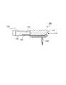
図1Aは、特許文献1に記載のマイクロ流路チップ10の平面図であり、図1Bは、図1AにおけるB−B線の断面図である。図1Aに示されるように、マイクロ流路チップ10は、溝および4つの貫通孔を含む基板18と、一方の面上に4つの電気伝達層(以下「伝達層」ともいう)28が配置されている、ガラスや樹脂などからなるプレート20とを有する。4つの貫通孔のうち2つの貫通孔は、溝の両端に連通している。溝の開口部がプレート20により閉塞されることで、マイクロチャネル(流路)14が形成される。また、4つの貫通孔の溝の開口部側の開口部がプレート20により閉塞されることで、4つのリザーバ26が形成される。プレート20は、基板18より面積が大きい。電気伝達層28は、一端がリザーバ26内に露出し、他端が基板18の外縁部よりも外側で外部に露出するようにプレート20上にそれぞれ配置されている。 FIG. 1A is a plan view of the
マイクロ流路チップ10の電気伝達層28の外部に露出した他端は、不図示のコネクタを介して測定機器などと接続される。マイクロ流路チップ10は、液体試料について種々の分析や処理などに使用されうる。 The other end exposed to the outside of the
特許文献1のマイクロ流路チップ10では、コネクタに接続される電気伝達層28の他端は、基板18の外縁部より外側において、十分な強度を有するプレート20の上に配置されている。このため、コネクタを電気伝達層28に押し当てるとき、十分な接触圧で接続することができる。一方で、小型化および製造コストの低減の観点から、プレート20の代わりにフィルムを使用したい場合もある。この場合、コネクタを電気伝達層28に接触させるときにフィルムが変形してしまうため、コネクタと電気伝達層28との間に十分な接触圧を得ることができないという問題がある。 In the
本発明は、かかる点に鑑みてなされたものであり、貫通孔または凹部を形成された基板に、一方の面上に伝達層を形成されたフィルムを接合することで製造されうる流体取扱装置であって、測定機器などのコネクタをフィルム上の伝達層に押し当てても十分な接触圧で接続することができる、流体取扱装置を提供することを目的とする。 The present invention has been made in view of such a point, and is a fluid handling apparatus that can be manufactured by bonding a film having a transfer layer formed on one side to a substrate having a through hole or a recess formed. An object of the present invention is to provide a fluid handling device which can be connected with sufficient contact pressure even when a connector such as a measuring device is pressed against a transfer layer on a film.
本発明者らは、伝達層を形成されたフィルムを折り曲げることで、測定機器などのコネクタをフィルム上の伝達層に押し当てても十分な接触圧で接続できることを見出し、さらに検討を加えて本発明を完成させた。 The present inventors have found that by bending the film on which the transfer layer is formed, even if a connector such as a measuring device is pressed against the transfer layer on the film, connection can be made with a sufficient contact pressure. Completed the invention.
すなわち、本発明は、以下の流体取扱装置に関する。 That is, the present invention relates to the following fluid handling device.
[1]貫通孔または凹部を含む基板と、第1領域、前記第1領域に隣接して配置された第2領域および前記第2領域に隣接して配置された第3領域を含むフィルムと、前記フィルムの一方の面上に、前記第1領域、前記第2領域および前記第3領域に亘って配置された、電気または熱を伝達する伝達層と、を有し、前記フィルムの前記第1領域は、前記貫通孔の一方の開口部または前記凹部の開口部を閉塞することで液体を収容可能な収容部を形成するように、かつ前記伝達層の一部が前記収容部内に露出するように前記基板の一方の面に接合され、前記フィルムの前記第2領域は、前記伝達層が外側に位置するように折り曲げられ、前記フィルムの前記第3領域は、前記伝達層が外部に露出するように前記フィルムの前記第1領域に接合されている、流体取扱装置。
[2]前記基板は、前記フィルムの前記第2領域と対向する位置に切り欠き部を有する、[1]に記載の流体取扱装置。
[3]前記収容部は、毛細管現象により液体が移動可能な流路を有する、[1]または[2]に記載の流体取扱装置。
[4]前記伝達層は、金属薄膜または導電性インク層である、[1]〜[3]のいずれか一つに記載の流体取扱装置。[1] A substrate including a through hole or a recess, a film including a first region, a second region disposed adjacent to the first region, and a third region disposed adjacent to the second region. A transfer layer for transferring electricity or heat disposed over the first area, the second area and the third area on one surface of the film; The area is closed so as to form a container capable of containing a liquid by closing one opening of the through hole or the opening of the recess, and a part of the transmission layer is exposed in the container. And the second region of the film is bent so that the transfer layer is located outside, and the third region of the film exposes the transfer layer to the outside. Bonded to the first region of the film And is, fluid handling equipment.
[2] The fluid handling device according to [1], wherein the substrate has a notch at a position facing the second region of the film.
[3] The fluid handling device according to [1] or [2], wherein the storage portion has a flow path through which liquid can be moved by capillary action.
[4] The fluid handling device according to any one of [1] to [3], wherein the transfer layer is a metal thin film or a conductive ink layer.
本発明によれば、貫通孔または凹部を形成された基板に、一方の面上に伝達層を形成されたフィルムを接合することで製造されうる流体取扱装置でありながら、測定機器などのコネクタをフィルム上の伝達層に押し当てても十分な接触圧で接続することができる。したがって、本発明に係る流体取扱装置は、例えば差し込み式のコネクタを有する測定機器などに適切に設置することができ、これにより微量な物質について正確に測定などを行うことができる。 According to the present invention, it is a fluid handling apparatus that can be manufactured by bonding a film having a transfer layer formed on one surface to a substrate having a through hole or a recess, but a connector such as a measuring device is used. Even if pressed against the transfer layer on the film, connection can be made with sufficient contact pressure. Therefore, the fluid handling device according to the present invention can be properly installed, for example, in a measuring device having a plug-in connector, whereby accurate measurement or the like of a trace amount of substance can be performed.
以下、本発明に係る実施の形態について、図面を参照して詳細に説明する。以下の説明では、本発明に係る流体取扱装置の代表例として、マイクロチップおよびマイクロ流路チップについて説明する。 Hereinafter, embodiments according to the present invention will be described in detail with reference to the drawings. In the following description, a microchip and a microchannel chip will be described as a representative example of the fluid handling device according to the present invention.
[実施の形態1]
実施の形態1では、試薬や液体試料などの液体の加熱処理などを行うことができるマイクロチップ100について説明する。First Embodiment
In the first embodiment, a
(マイクロチップの構成)
図2および図3は、本発明の実施の形態1に係るマイクロチップ100の構成を示す図である。図2Aは、マイクロチップ100の平面図であり、図2Bは、図2Aに示されるB−B線の断面図であり、図2Cは、図2Aに示されるC−C線の断面図である。図3Aは、基板110の平面図であり、図3Bは、伝達層130が形成されたフィルム120の平面図である。(Configuration of microchip)
2 and 3 are diagrams showing the configuration of the
図2A〜Cに示されるように、マイクロチップ100は、収容部113を有する板状のデバイスである。マイクロチップ100は、基板110、フィルム120および伝達層130を有する。フィルム120は、第1領域121、第2領域122および第3領域123を含む。 As shown in FIGS. 2A to 2C, the
基板110は、透明な略矩形の部材であり、貫通孔111および切り欠き部112を有する。貫通孔111は、基板110の両面に開口している。貫通孔111は、フィルム120により一方の開口部を閉塞されることで、液体を収容可能な収容部113となる。貫通孔111の形状および大きさは、特に限定されず、用途に応じて適宜設定されうる。たとえば、貫通孔111の形状は、直径0.1〜10mmの略円柱状である。 The
切り欠き部112は、フィルム120の第2領域122と対向する位置に設けられている。本実施の形態では、切り欠き部112は、基板110の裏側の端部に設けられている。図2Bに示されるように、切り欠き部112には、フィルム120の第2領域122が収められる。切り欠き部112の形状および大きさは、フィルム120の第2領域122を収めることができれば特に限定されない。たとえば、切り欠き部112の形状は、角柱状である。本実施の形態では、切り欠き部112の形状は、略三角柱状である。また、たとえば、伝達層130の長さ方向における切り欠き部112の幅は0.5〜5mm程度であり、切り欠き部112の基板110の厚さ方向の長さは0.5〜5mm程度である。 The
基板110の大きさおよび厚さは、特に限定されず、用途に応じて適宜設定されうる。たとえば、基板110の大きさは、10mm×20mmであり、基板110の厚さは、1〜10mmである。基板110を構成する材料は、特に限定されず、公知の樹脂およびガラスから用途に応じて適宜選択することができる。基板110の材料の例には、ポリエチレンテレフタレート、ポリカーボネート、ポリメタクリル酸メチル、塩化ビニール、ポリプロピレン、ポリエーテル、ポリエチレンなどが含まれる。 The size and thickness of the
フィルム120は、透明な略矩形の樹脂フィルムである。図3Bに示されるように、フィルム120は、第1領域121、第1領域121に隣接して配置された第2領域122および第2領域122に隣接して配置された第3領域123を含む。前述のとおり、フィルム120は、基板110の貫通孔111の一方の開口部を閉塞することで収容部113を形成する。フィルム120の第1領域121は、貫通孔111の一方の開口部を閉塞するように、かつ伝達層130の一部が収容部113内に露出するように基板110の一方の面(裏側の面)に接合されている。フィルム120の第1領域121を基板110に接合させる方法は、特に限定されないが、収容部113に、液体試料を導入したときに液体試料が外部に漏出するのを防ぐ観点から、フィルム120は、基板110との間に隙間がないように接合される。たとえば、フィルム120は、熱圧着や接着剤による接着などにより基板110に接合される。 The
フィルム120の第2領域122は、伝達層130が外側に位置するように折り曲げられている。フィルム120の第2領域122(折り曲げ部)は、切り欠き部112内に収められる。これにより、マイクロチップ100をヒータなどに接続するときに、フィルム120の折り曲げ部が基板110の厚さ方向に突出することが防止される。 The
フィルム120の第3領域123は、伝達層130が外部に露出するようにフィルム120の第1領域121に接合されている。フィルム120の第3領域123をフィルム120の第1領域121に接合させる方法は、特に限定されない。たとえば、フィルム120の第3領域123は、フィルム120の第1領域121を基板110に接合させる場合と同様の方法により接合される。 The
フィルム120の厚さは、収容部113に要求される強度を確保できれば特に限定されない。たとえば、フィルム120の厚さは、100μm程度である。 The thickness of the
フィルム120を構成する材料は、柔軟性のある材料であれば特に限定されないが、通常は樹脂である。フィルム120を構成する樹脂の例には、ポリエチレンテレフタレート、ポリカーボネート、ポリオレフィン、アクリル樹脂、シクロオレフィンポリマー(COP)などが含まれる。基板110とフィルム120との密着性を向上させる観点から、フィルム120を構成する材料は、基板110を構成する材料と同一であることが好ましい。 Although the material which comprises the
伝達層130は、図3Bに示されるように、フィルム120の一方の面上に、第1領域121、第2領域122および第3領域123に亘って配置された、電気または熱を伝達できる層である。たとえば、伝達層130は、金属薄膜や導電性インク層(例えばカーボンインク層)などである。図2Bに示されるように、フィルム120の第1領域121上に配置された伝達層130は、その一部が収容部113内に露出するように基板110の一方の面側(裏側)に配置されている。フィルム120の第2領域122上に配置された伝達層130は、折り曲げられたフィルム120の外側に位置するように配置されている。フィルム120の第3領域123上に配置された伝達層130は、外部に露出するように配置されている。伝達層130は、電極、電熱ヒータ、pHや温度、流量、などのセンサ、または電気化学的ディテクタとして使用されうる。本実施の形態では、伝達層130は、電熱ヒータとして使用されうる。 The
伝達層130の形状および厚さは、液体試料の測定や処理などに十分な熱または電気を伝達することができれば特に限定されず、用途に応じて適宜設定されうる。たとえば、伝達層130の幅は、0.1〜1mm程度であり、伝達層130の厚さは、10μm程度である。 The shape and thickness of the
(マイクロチップの製造方法)
次に、図4を参照して、実施の形態1に係るマイクロチップ100の製造方法について説明する。マイクロチップ100は、以下に述べる工程により製造されうる。(Method of manufacturing microchip)
Next, with reference to FIG. 4, a method of manufacturing the
図4は、実施の形態1に係るマイクロチップ100の製造方法を説明するための断面図である。まず、図4Aに示されるように、基板110と、伝達層130が形成されたフィルム120とを準備する。基板110には、貫通孔111および切り欠き部112が形成されている。基板110に貫通孔111および切り欠き部112を形成する方法は、特に限定されない。たとえば、金型成形法やリソグラフィ法などにより貫通孔111および切り欠き部112を形成すればよい。伝達層130を形成する方法も特に限定されない。伝達層130は、例えば導電性ペーストのスクリーン印刷などにより形成すればよい。 FIG. 4 is a cross-sectional view for explaining the method of manufacturing the
次いで、図4Bに示されるように、伝達層130が形成されたフィルム120の第1領域121を基板110の裏側の面に、伝達層130の一部が貫通孔111内に露出するように配置する。次いで、図4Cに示されるように、フィルム120の第1領域121を基板110に熱圧着により接合させる。これにより、収容部113が形成される。次いで、図4Dに示されるように、フィルム120の第2領域122を伝達層130が外側に位置するように折り曲げ、フィルム120の第3領域123を熱圧着により第1領域121に接合させる。このとき、フィルム120の第2領域122(折り曲げ部)は、切り欠き部112内に収められ、基板110の厚さ方向に突出しない。伝達層130の一端は、基板110の裏側において収容部113内に露出し、伝達層130の他端は、基板110の裏側において外部に露出する。以上の工程により、本実施の形態に係るマイクロチップ100を製造することができる。 Next, as shown in FIG. 4B, the
このようにして製造されたマイクロチップ100では、伝達層130の他端を裏打ちするフィルム120の第3領域123は、フィルム120の第1領域121および伝達層130を挟んで基板110上に配置される。このため、後述するとおり、伝達層130の他端と加熱用ヒータとを十分な接触圧で接続することができる。 In the
従来、伝達層の一端を収容部内に露出させつつ、伝達層の他端を外部に露出させる方法として、フィルムの両面に伝達層を形成し、これらをスルーホール配線で接続する方法が知られている。これに対し本発明では、フィルム120の一方の面にのみ伝達層130を形成しつつも、伝達層130の一端を収容部113内に露出させ、かつ伝達層130の他端を外部に露出させることを実現している。したがって、マイクロチップ100は、両面印刷を用いることなく、安価に製造されうる。 Conventionally, as a method of exposing the other end of the transmission layer to the outside while exposing one end of the transmission layer in the housing portion, a method is known in which the transmission layer is formed on both sides of the film and these are connected by through hole wiring. There is. On the other hand, in the present invention, while the
(マイクロチップの使用方法)
次に、図5を参照して、実施の形態1に係るマイクロチップ100の使用方法について説明する。(How to use the microchip)
Next, a method of using the
図5は、実施の形態1に係るマイクロチップ100の使用態様を説明するための図である。図5に示されるように、マイクロチップ100の収容部113に試薬や液体試料などの液体115が提供される。伝達層130には、ヒータ135が押し当てられる。伝達層130は、フィルム120および伝達層130を挟んで基板110上に配置されているため、ヒータ135を十分な接触圧で接続することができる。また、このように基板110の外縁部より内側において伝達層130およびヒータ135を接続することができるため、マイクロチップ100を小型化することができる(図1Bと図5とを比較参照)。さらに、この状態で熱源を加熱すると、伝達層130を介して収容部113内の液体115を加熱することができる。 FIG. 5 is a diagram for describing a use mode of the
(効果)
以上のように、実施の形態1に係るマイクロチップ100では、フィルム120を折り曲げることで伝達層130の一端を収容部113内に露出させつつ、伝達層130の他端を外部に露出させている。伝達層130およびヒータ135は、基板110上において安定した状態で接触することができる。このため、伝達層130およびヒータ135は、十分な接触圧で接続されうる。実施の形態1に係るマイクロチップ100は、ヒータ以外にも、例えば差し込み式のコネクタを有する測定機器などに適切に設置することができ、これにより微量な物質について正確に測定や処理などを行うことができる。(effect)
As described above, in the
なお、本実施の形態では、伝達層130を加熱処理用のヒータとして用いたが、伝達層の用途は、加熱処理用のヒータに限定されるものではない。 Although the
また、基板の形状も、図3Aおよび図4Aに示される形状に限定されるものではない。図6は、実施の形態1の変形例に係るマイクロチップ100’の断面図である。本実施の形態では、切り欠き部112を有する基板110を用いたマイクロチップ100について説明したが、図6に示されるように、切り欠き部112を有しない基板110’を用いてもよい。フィルム120の第2領域122は、伝達層130が外側に位置するように折り曲げられる。このとき、フィルム120の第2領域122が基板110’の厚さ方向に突出することを防止する観点から、フィルム120の第2領域122は、基板110’の外縁部より外側に配置されることが好ましい。 Also, the shape of the substrate is not limited to the shapes shown in FIGS. 3A and 4A. FIG. 6 is a cross-sectional view of a microchip 100 'according to a modification of the first embodiment. In the present embodiment, the
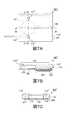
また、本実施の形態では、基板110の貫通孔111の開口部をフィルム120で閉塞することで形成された収容部113を有するマイクロチップ100について説明した。しかしながら、基板110は、貫通孔111の代わりに収容部113となる凹部を有していてもよい。図7Aは、実施の形態1の変形例に係るマイクロチップ100”の平面図であり、図7Bは、図7Aに示されるB−B線の断面図であり、図7Cは、図7Aに示されるC−C線の断面図である。 Further, in the present embodiment, the
図7A〜Cに示されるように、基板110”は、貫通孔111の代わりに凹部111”を有している。フィルム120の第1領域121は、凹部111”の開口部を閉塞することで液体を収容可能な収容部113”を形成する。また、基板110”は、2つの第2貫通孔と2つの溝とをさらに有する。フィルム120の第1領域121は、2つの第2貫通孔の開口部を閉塞することで液体を収容部113”に導入するための注入口117”および排出口118”を形成する。また、フィルム120の第1領域121は、2つの溝の開口部を閉塞することで液体が流れる流路119”を形成する。2つの流路119”の一端は、収容部113”にそれぞれ連通し、2つの流路119”の他端は、注入口117”または排出口118”にそれぞれ連通する。これにより、液体を外部から収容部113”に導入することができる。 As shown in FIGS. 7A to 7C, the
[実施の形態2]
実施の形態2では、毛細管現象により液体が移動可能な流路217を有し、試薬や液体試料などに電圧を印加することができるマイクロ流路チップ200について説明する。Second Embodiment
In the second embodiment, a
実施の形態2に係るマイクロ流路チップ200は、基板210および伝達層230が実施の形態1に係るマイクロチップ100と異なる。そこで、実施の形態1に係るマイクロチップ100と同一の構成要素については、同一の符号を付してその説明を省略し、マイクロチップ100の基板110および伝達層130と異なる構成要素を中心に説明する。 The
(マイクロ流路チップの構成)
図8は、実施の形態2に係るマイクロ流路チップ200の構成を示す図である。図8Aは、マイクロ流路チップ200の平面図であり、図8Bは、図8Aに示されるB−B線の断面図であり、図8Cは、図8Aに示されるC−C線の断面図である。(Configuration of microchannel chip)
FIG. 8 is a diagram showing the configuration of the
図8A〜Cに示されるように、マイクロ流路チップ200は、基板210、フィルム120および2つの伝達層230を有する。 As shown in FIGS. 8A to 8C, the
基板210は、透明な略矩形の部材である。基板210は、溝214、第3貫通孔215、第4貫通孔216および切り欠き部112を有する。溝214は、基板210の一方の面(裏面)に開口している。溝214は、フィルム120によりその開口部が閉塞されることで、液体が流れる流路217となる。溝214の流れ方向に直交する断面形状は、特に限定されないが、例えば一辺の長さ(幅および深さ)が数十μm程度の略矩形である。 The
第3貫通孔215および第4貫通孔216は、基板210の両面にそれぞれ開口している。第3貫通孔215は、溝214の一方の端部に連通している。また、第4貫通孔216は、溝214の他方の端部に連通している。第3貫通孔215および第4貫通孔216の形状は、特に限定されないが、例えば略円柱状である。第3貫通孔215および第4貫通孔216の大きさは同じであってもよいし、異なっていてもよい。第3貫通孔215および第4貫通孔216の直径は、特に限定されないが、例えば0.1〜3mm程度である。切り欠き部112の形状および大きさについては、実施の形態1と同様であるためその説明を省略する。 The third through
基板210の大きさ、厚さおよび基板210を構成する材料についても、実施の形態1に係る基板110と同様であるため、その説明を省略する。 The size and thickness of the
本実施の形態では、フィルム120は、基板210の溝214、第3貫通孔215および第4貫通孔216の開口部を閉塞することで流路217、第1凹部218および第2凹部219を含む収容部213を形成する。具体的には、溝214の開口部がフィルム120により閉塞されることで、毛細管現象により液体が移動可能な流路217が形成される。また、基板210の第3貫通孔215および第4貫通孔216の溝214の開口部側の開口部が閉塞されることで、第1凹部218および第2凹部219が形成される。第1凹部218および第2凹部219は、流路217を介して互いに連通している。 In the present embodiment, the
2つの伝達層230は、図8A〜Cに示されるように、フィルム120の一方の面上に、第1領域121、第2領域122および第3領域123に亘って配置された、電気または熱を伝達することができる層である。フィルム120の第1領域121上に配置された伝達層230は、その一部が流路217内に露出するように基板210の一方の面側(裏側)にそれぞれ配置されている。フィルム120の第2領域122上に配置された伝達層230は、折り曲げられたフィルム120の外側に位置するように配置されている。フィルム120の第3領域123上に配置された伝達層230は、外部に露出するように配置されている。伝達層230の材料、厚さおよび用途などについては、実施の形態1と同様であるため、その説明を省略する。 The two
本実施の形態に係るマイクロ流路チップ200では、伝達層230は、不図示の電極コネクタを介して外部電源に接続される。流路217内に液体試料が存在する状態で2つの伝達層230間に電圧を印加することで、流路217内の液体試料に電圧を印加することができる。また、本実施の形態においても、伝達層230は、フィルム120および伝達層230を挟んで基板210上に配置されているため、電極コネクタを十分な接触圧で接続することができる。また、このように基板210の外縁部より内側において伝達層230および電極コネクタを接続することができるため、マイクロ流路チップ200を小型化することができる。 In the
(効果)
以上のように、実施の形態2に係るマイクロ流路チップ200では、フィルム120を折り曲げることで伝達層230の一端を流路217内に露出させつつ、伝達層230の他端を外部に露出させている。伝達層230および電極コネクタは、基板210上において安定した状態で接触することができる。このため、伝達層230および電極コネクタは、十分な接触圧で接続されうる。実施の形態2に係るマイクロ流路チップ200は、例えば差し込み式の電極コネクタを有する測定機器などに適切に設置することができ、これにより微量な物質について正確に測定や処理などを行うことができる。(effect)
As described above, in the
なお、実施の形態2に係るマイクロ流路チップ200では、伝達層230を電圧印加用の電極として用いたが、伝達層の用途は、電圧印加用の電極に限定されるものではない。 In the
また、実施の形態1および実施の形態2では、マイクロチップ100およびマイクロ流路チップ200を液体試料の処理や分析などに使用する場合について説明したが、本発明に係る流体取扱装置は、液体以外の流体(例えば、混合物、スラリー、懸濁液など)の処理や分析などに使用してもよい。 In the first and second embodiments, the
本発明の流体取扱装置は、例えば、科学分野や医学分野などにおいて微量な物質の分析などに使用されるマイクロチップまたはマイクロ流路チップとして有用である。 The fluid handling device of the present invention is useful, for example, as a microchip or a microchannel chip used for analysis of a small amount of substance in the scientific field, medical field, and the like.
10 マイクロ流路チップ
14 マイクロチャネル(流路)
18 基板
20 プレート
26 リザーバ
28 電気伝達層
100、100’、100”、200 マイクロ(流路)チップ
110、110’、110”、210 基板
111 貫通孔
111” 凹部
112 切り欠き部
113、113”、213 収容部
115 液体
117” 注入口
118” 排出口
119” 流路
120 フィルム
121 第1領域
122 第2領域
123 第3領域
130、230 伝達層
135 ヒータ
214 溝
215 第3貫通孔
216 第4貫通孔
217 流路
218 第1凹部
219 第2凹部10
18
Claims (4)
Translated fromJapanese第1領域、前記第1領域に隣接して配置された第2領域および前記第2領域に隣接して配置された第3領域を含むフィルムと、
前記フィルムの一方の面上に、前記第1領域、前記第2領域および前記第3領域に亘って配置された、電気または熱を伝達する伝達層と、
を有し、
前記フィルムの前記第1領域は、前記貫通孔の一方の開口部または前記凹部の開口部を閉塞することで液体を収容可能な収容部を形成するように、かつ前記伝達層の一部が前記収容部内に露出するように前記基板の一方の面に接合され、
前記フィルムの前記第2領域は、前記伝達層が外側に位置するように折り曲げられ、
前記フィルムの前記第3領域は、前記伝達層が外部に露出するように前記フィルムの前記第1領域に接合されており、
前記貫通孔の前記一方の開口部の縁または前記凹部の前記開口部の縁において、前記フィルムおよび前記伝達層の少なくとも一部は、前記貫通孔の内側または前記凹部の内側に向けて折り曲げられている、
流体取扱装置。A substrate comprising through holes or recesses,
A film including a first region, a second region disposed adjacent to the first region, and a third region disposed adjacent to the second region;
A transfer layer for transferring electricity or heat, disposed over the first area, the second area and the third area on one side of the film;
Have
The first region of the film forms a container capable of containing a liquid by closing one opening of the through hole or the opening of the recess, and a part of the transmission layer is Bonded to one side of the substrate so as to be exposed in the housing portion,
The second region of the film is folded so that the transfer layer is located on the outside,
The third region of the film, the transfer layeris joined to the first region of the film so as to be exposed to the outside,
At the edge of the one opening of the through hole or the edge of the opening of the recess, at least a part of the film and the transfer layer is bent toward the inside of the through hole or the inside of the recess Yes,
Fluid handling equipment.
Priority Applications (3)
| Application Number | Priority Date | Filing Date | Title |
|---|---|---|---|
| JP2014123551AJP6549355B2 (en) | 2014-06-16 | 2014-06-16 | Fluid handling device |
| US14/731,491US9387477B2 (en) | 2014-06-16 | 2015-06-05 | Fluid handling device |
| EP15171264.3AEP2957343B1 (en) | 2014-06-16 | 2015-06-09 | Fluid handling device |
Applications Claiming Priority (1)
| Application Number | Priority Date | Filing Date | Title |
|---|---|---|---|
| JP2014123551AJP6549355B2 (en) | 2014-06-16 | 2014-06-16 | Fluid handling device |
Publications (2)
| Publication Number | Publication Date |
|---|---|
| JP2016003922A JP2016003922A (en) | 2016-01-12 |
| JP6549355B2true JP6549355B2 (en) | 2019-07-24 |
Family
ID=53719606
Family Applications (1)
| Application Number | Title | Priority Date | Filing Date |
|---|---|---|---|
| JP2014123551AExpired - Fee RelatedJP6549355B2 (en) | 2014-06-16 | 2014-06-16 | Fluid handling device |
Country Status (3)
| Country | Link |
|---|---|
| US (1) | US9387477B2 (en) |
| EP (1) | EP2957343B1 (en) |
| JP (1) | JP6549355B2 (en) |
Families Citing this family (4)
| Publication number | Priority date | Publication date | Assignee | Title |
|---|---|---|---|---|
| US11674919B2 (en)* | 2019-07-17 | 2023-06-13 | Taiwan Semiconductor Manufacturing Company Ltd. | Detector, detection device and method of using the same |
| JP7339603B2 (en)* | 2019-08-30 | 2023-09-06 | ウシオ電機株式会社 | microchip |
| FR3114253B1 (en) | 2020-09-21 | 2022-08-26 | Commissariat Energie Atomique | Fluidic system comprising a fluidic component and an instrumented device fitted to said component |
| JP2024077053A (en)* | 2022-11-28 | 2024-06-07 | デクセリアルズ株式会社 | Sheet-like structure and method of using same |
Family Cites Families (16)
| Publication number | Priority date | Publication date | Assignee | Title |
|---|---|---|---|---|
| US6939451B2 (en)* | 2000-09-19 | 2005-09-06 | Aclara Biosciences, Inc. | Microfluidic chip having integrated electrodes |
| DK2461156T3 (en) | 2001-06-29 | 2020-08-03 | Meso Scale Technologies Llc | Device for luminescence test measurements |
| US7005179B2 (en)* | 2002-07-26 | 2006-02-28 | The Regents Of The University Of California | Conductive inks for metalization in integrated polymer microsystems |
| US7226564B2 (en)* | 2002-07-26 | 2007-06-05 | Enplas Corporation | Plate assembly |
| DE10234819A1 (en)* | 2002-07-31 | 2004-02-19 | Roche Diagnostics Gmbh | Test apparatus for blood, comprising compound body with test strip levels and transport channels to give complex tests in compact structure |
| US7338637B2 (en)* | 2003-01-31 | 2008-03-04 | Hewlett-Packard Development Company, L.P. | Microfluidic device with thin-film electronic devices |
| US7347617B2 (en)* | 2003-08-19 | 2008-03-25 | Siemens Healthcare Diagnostics Inc. | Mixing in microfluidic devices |
| JP4475986B2 (en)* | 2004-03-09 | 2010-06-09 | 株式会社エンプラス | Intermediate connector for electrical component socket and electrical component socket |
| US20060060769A1 (en)* | 2004-09-21 | 2006-03-23 | Predicant Biosciences, Inc. | Electrospray apparatus with an integrated electrode |
| JP5385607B2 (en)* | 2005-07-20 | 2014-01-08 | バイエル・ヘルスケア・エルエルシー | Gated current measuring instrument |
| KR101577176B1 (en)* | 2005-09-30 | 2015-12-14 | 바이엘 헬스케어 엘엘씨 | Gated voltammetry analyte determination |
| EP2350634B1 (en)* | 2008-11-04 | 2015-01-21 | Etat Français Représenté Par Le Délégué Général Pour L'Armement | Microfluidic device for the separation or fractioning or preconcentration of analytes contained in an electrolyte |
| US8206664B2 (en)* | 2010-07-06 | 2012-06-26 | Xerox Corporation | Methods of producing multi-layered microfluidic devices |
| JP5797926B2 (en)* | 2011-04-21 | 2015-10-21 | 株式会社エンプラス | Fluid handling apparatus, manufacturing method thereof, and fluid handling system |
| JP6047352B2 (en)* | 2012-09-20 | 2016-12-21 | 株式会社エンプラス | Fluid handling equipment |
| JP2014097485A (en)* | 2012-10-18 | 2014-05-29 | Enplas Corp | Liquid handling apparatus |
- 2014
- 2014-06-16JPJP2014123551Apatent/JP6549355B2/ennot_activeExpired - Fee Related
- 2015
- 2015-06-05USUS14/731,491patent/US9387477B2/ennot_activeExpired - Fee Related
- 2015-06-09EPEP15171264.3Apatent/EP2957343B1/ennot_activeNot-in-force
Also Published As
| Publication number | Publication date |
|---|---|
| EP2957343A1 (en) | 2015-12-23 |
| US20150360223A1 (en) | 2015-12-17 |
| EP2957343B1 (en) | 2018-10-10 |
| JP2016003922A (en) | 2016-01-12 |
| US9387477B2 (en) | 2016-07-12 |
Similar Documents
| Publication | Publication Date | Title |
|---|---|---|
| EP2827988B1 (en) | Compact fluid analysis device and method to fabricate | |
| US6251343B1 (en) | Microfluidic devices and systems incorporating cover layers | |
| US9579649B2 (en) | Fluid delivery manifolds and microfluidic systems | |
| JP5797926B2 (en) | Fluid handling apparatus, manufacturing method thereof, and fluid handling system | |
| JP2016179198A5 (en) | ||
| JP6549355B2 (en) | Fluid handling device | |
| US9927421B2 (en) | Sample chamber | |
| JP2008284626A (en) | Microchannel device | |
| EP3223945B1 (en) | Compact glass-based fluid analysis device and method to fabricate | |
| JP6047352B2 (en) | Fluid handling equipment | |
| JP6310327B2 (en) | Fluid handling equipment | |
| CN104668002B (en) | Compact fluid analysis device and method of manufacturing the same | |
| JP5723198B2 (en) | Fluid handling device and fluid handling system | |
| US11484876B2 (en) | Systems and methods for an e-gating feature in an electrochemical test strip | |
| US9901924B2 (en) | Fluid handling device, fluid handling method, and fluid handling system | |
| JP5723197B2 (en) | Fluid handling device and fluid handling system | |
| US20220018744A1 (en) | Bridging liquid between microfluidic elements without closed channels | |
| US20130210070A1 (en) | Microfluidic device and method for controlling interaction between liquids |
Legal Events
| Date | Code | Title | Description |
|---|---|---|---|
| A621 | Written request for application examination | Free format text:JAPANESE INTERMEDIATE CODE: A621 Effective date:20170508 | |
| A977 | Report on retrieval | Free format text:JAPANESE INTERMEDIATE CODE: A971007 Effective date:20180125 | |
| A131 | Notification of reasons for refusal | Free format text:JAPANESE INTERMEDIATE CODE: A131 Effective date:20180227 | |
| A131 | Notification of reasons for refusal | Free format text:JAPANESE INTERMEDIATE CODE: A131 Effective date:20181009 | |
| A521 | Request for written amendment filed | Free format text:JAPANESE INTERMEDIATE CODE: A523 Effective date:20181204 | |
| TRDD | Decision of grant or rejection written | ||
| RD02 | Notification of acceptance of power of attorney | Free format text:JAPANESE INTERMEDIATE CODE: A7422 Effective date:20190617 | |
| A01 | Written decision to grant a patent or to grant a registration (utility model) | Free format text:JAPANESE INTERMEDIATE CODE: A01 Effective date:20190618 | |
| A61 | First payment of annual fees (during grant procedure) | Free format text:JAPANESE INTERMEDIATE CODE: A61 Effective date:20190627 | |
| R150 | Certificate of patent or registration of utility model | Ref document number:6549355 Country of ref document:JP Free format text:JAPANESE INTERMEDIATE CODE: R150 | |
| LAPS | Cancellation because of no payment of annual fees |