JP6545083B2 - Touch screen, touch panel, display device and electronic device - Google Patents
Touch screen, touch panel, display device and electronic deviceDownload PDFInfo
- Publication number
- JP6545083B2 JP6545083B2JP2015219262AJP2015219262AJP6545083B2JP 6545083 B2JP6545083 B2JP 6545083B2JP 2015219262 AJP2015219262 AJP 2015219262AJP 2015219262 AJP2015219262 AJP 2015219262AJP 6545083 B2JP6545083 B2JP 6545083B2
- Authority
- JP
- Japan
- Prior art keywords
- touch screen
- capacitance
- terminal
- lead
- wiring
- Prior art date
- Legal status (The legal status is an assumption and is not a legal conclusion. Google has not performed a legal analysis and makes no representation as to the accuracy of the status listed.)
- Active
Links
Images


Classifications
- G—PHYSICS
- G06—COMPUTING OR CALCULATING; COUNTING
- G06F—ELECTRIC DIGITAL DATA PROCESSING
- G06F3/00—Input arrangements for transferring data to be processed into a form capable of being handled by the computer; Output arrangements for transferring data from processing unit to output unit, e.g. interface arrangements
- G06F3/01—Input arrangements or combined input and output arrangements for interaction between user and computer
- G06F3/03—Arrangements for converting the position or the displacement of a member into a coded form
- G06F3/041—Digitisers, e.g. for touch screens or touch pads, characterised by the transducing means
- G06F3/0412—Digitisers structurally integrated in a display
- G—PHYSICS
- G02—OPTICS
- G02F—OPTICAL DEVICES OR ARRANGEMENTS FOR THE CONTROL OF LIGHT BY MODIFICATION OF THE OPTICAL PROPERTIES OF THE MEDIA OF THE ELEMENTS INVOLVED THEREIN; NON-LINEAR OPTICS; FREQUENCY-CHANGING OF LIGHT; OPTICAL LOGIC ELEMENTS; OPTICAL ANALOGUE/DIGITAL CONVERTERS
- G02F1/00—Devices or arrangements for the control of the intensity, colour, phase, polarisation or direction of light arriving from an independent light source, e.g. switching, gating or modulating; Non-linear optics
- G02F1/01—Devices or arrangements for the control of the intensity, colour, phase, polarisation or direction of light arriving from an independent light source, e.g. switching, gating or modulating; Non-linear optics for the control of the intensity, phase, polarisation or colour
- G02F1/13—Devices or arrangements for the control of the intensity, colour, phase, polarisation or direction of light arriving from an independent light source, e.g. switching, gating or modulating; Non-linear optics for the control of the intensity, phase, polarisation or colour based on liquid crystals, e.g. single liquid crystal display cells
- G02F1/133—Constructional arrangements; Operation of liquid crystal cells; Circuit arrangements
- G02F1/1333—Constructional arrangements; Manufacturing methods
- G02F1/13338—Input devices, e.g. touch panels
- G—PHYSICS
- G06—COMPUTING OR CALCULATING; COUNTING
- G06F—ELECTRIC DIGITAL DATA PROCESSING
- G06F3/00—Input arrangements for transferring data to be processed into a form capable of being handled by the computer; Output arrangements for transferring data from processing unit to output unit, e.g. interface arrangements
- G06F3/01—Input arrangements or combined input and output arrangements for interaction between user and computer
- G06F3/03—Arrangements for converting the position or the displacement of a member into a coded form
- G06F3/041—Digitisers, e.g. for touch screens or touch pads, characterised by the transducing means
- G06F3/0416—Control or interface arrangements specially adapted for digitisers
- G06F3/0418—Control or interface arrangements specially adapted for digitisers for error correction or compensation, e.g. based on parallax, calibration or alignment
- G—PHYSICS
- G06—COMPUTING OR CALCULATING; COUNTING
- G06F—ELECTRIC DIGITAL DATA PROCESSING
- G06F3/00—Input arrangements for transferring data to be processed into a form capable of being handled by the computer; Output arrangements for transferring data from processing unit to output unit, e.g. interface arrangements
- G06F3/01—Input arrangements or combined input and output arrangements for interaction between user and computer
- G06F3/03—Arrangements for converting the position or the displacement of a member into a coded form
- G06F3/041—Digitisers, e.g. for touch screens or touch pads, characterised by the transducing means
- G06F3/044—Digitisers, e.g. for touch screens or touch pads, characterised by the transducing means by capacitive means
- G06F3/0445—Digitisers, e.g. for touch screens or touch pads, characterised by the transducing means by capacitive means using two or more layers of sensing electrodes, e.g. using two layers of electrodes separated by a dielectric layer
- G—PHYSICS
- G06—COMPUTING OR CALCULATING; COUNTING
- G06F—ELECTRIC DIGITAL DATA PROCESSING
- G06F3/00—Input arrangements for transferring data to be processed into a form capable of being handled by the computer; Output arrangements for transferring data from processing unit to output unit, e.g. interface arrangements
- G06F3/01—Input arrangements or combined input and output arrangements for interaction between user and computer
- G06F3/03—Arrangements for converting the position or the displacement of a member into a coded form
- G06F3/041—Digitisers, e.g. for touch screens or touch pads, characterised by the transducing means
- G06F3/044—Digitisers, e.g. for touch screens or touch pads, characterised by the transducing means by capacitive means
- G06F3/0446—Digitisers, e.g. for touch screens or touch pads, characterised by the transducing means by capacitive means using a grid-like structure of electrodes in at least two directions, e.g. using row and column electrodes
- G—PHYSICS
- G06—COMPUTING OR CALCULATING; COUNTING
- G06F—ELECTRIC DIGITAL DATA PROCESSING
- G06F2203/00—Indexing scheme relating to G06F3/00 - G06F3/048
- G06F2203/041—Indexing scheme relating to G06F3/041 - G06F3/045
- G06F2203/04107—Shielding in digitiser, i.e. guard or shielding arrangements, mostly for capacitive touchscreens, e.g. driven shields, driven grounds
- G—PHYSICS
- G06—COMPUTING OR CALCULATING; COUNTING
- G06F—ELECTRIC DIGITAL DATA PROCESSING
- G06F2203/00—Indexing scheme relating to G06F3/00 - G06F3/048
- G06F2203/041—Indexing scheme relating to G06F3/041 - G06F3/045
- G06F2203/04111—Cross over in capacitive digitiser, i.e. details of structures for connecting electrodes of the sensing pattern where the connections cross each other, e.g. bridge structures comprising an insulating layer, or vias through substrate
- G—PHYSICS
- G06—COMPUTING OR CALCULATING; COUNTING
- G06F—ELECTRIC DIGITAL DATA PROCESSING
- G06F3/00—Input arrangements for transferring data to be processed into a form capable of being handled by the computer; Output arrangements for transferring data from processing unit to output unit, e.g. interface arrangements
- G06F3/01—Input arrangements or combined input and output arrangements for interaction between user and computer
- G06F3/03—Arrangements for converting the position or the displacement of a member into a coded form
- G06F3/041—Digitisers, e.g. for touch screens or touch pads, characterised by the transducing means
- G06F3/0416—Control or interface arrangements specially adapted for digitisers
- G06F3/04164—Connections between sensors and controllers, e.g. routing lines between electrodes and connection pads
Landscapes
- Engineering & Computer Science (AREA)
- General Engineering & Computer Science (AREA)
- Theoretical Computer Science (AREA)
- Physics & Mathematics (AREA)
- General Physics & Mathematics (AREA)
- Human Computer Interaction (AREA)
- Nonlinear Science (AREA)
- Mathematical Physics (AREA)
- Chemical & Material Sciences (AREA)
- Crystallography & Structural Chemistry (AREA)
- Optics & Photonics (AREA)
- Position Input By Displaying (AREA)
Description
Translated fromJapanese本発明は、タッチスクリーン、当該タッチスクリーンを備えるタッチパネル、当該タッチパネルを備える表示装置および電子機器に関する。 The present invention relates to a touch screen, a touch panel including the touch screen, a display device including the touch panel, and an electronic apparatus.
タッチパネルは、指などの指示体によるタッチを検出して、タッチパネルにおけるタッチされた位置の位置座標を特定する装置であり、優れたユーザーインターフェース手段の1つとして注目されている。現在、抵抗膜方式、静電容量方式などの種々の方式のタッチパネルが製品化されている。一般的に、タッチパネルは、タッチセンサ(タッチを検出するセンサ)が内蔵されたタッチスクリーンと、当該タッチスクリーンから入力された信号に基づいてタッチされた位置の位置座標を特定する検出装置とを備えている。 The touch panel is a device that detects a touch by an indicator such as a finger to specify position coordinates of a touched position on the touch panel, and is noted as one of excellent user interface means. Currently, touch panels of various types such as a resistance film type and a capacitance type are put on the market. Generally, the touch panel includes a touch screen (a sensor for detecting a touch) and a detection device for specifying position coordinates of a touched position based on a signal input from the touch screen. ing.
静電容量方式のタッチパネルの1つとして、投影型静電容量(Projected Capacitive)方式のタッチパネルがある(例えば、特許文献1参照)。特許文献1のような投影型静電容量方式のタッチパネルは、タッチセンサが内蔵されたタッチスクリーンの前面側を厚さ数mm程度のガラス板などの保護板で覆った場合であってもタッチを検出することが可能である。投影型静電容量方式のタッチパネルは、保護板をタッチスクリーンの前面側に配置することができるため堅牢性に優れる。また、使用者が手袋を装着した状態でタッチした場合であっても、タッチを検出することが可能である。さらに、可動部を有さず、当該可動部の可動に起因する不具合等が生じないため長寿命である。 As one of the capacitive touch panels, there is a Projected Capacitive touch panel (see, for example, Patent Document 1). The touch panel of the projection type electrostatic capacity method like
投影型静電容量方式のタッチパネルは、例えば、静電容量を検出するための検出用配線として、薄い誘電膜上に形成された第1シリーズの導体エレメントと、第1シリーズの導体エレメント上に絶縁膜を隔てて形成された第2シリーズの導体エレメントとを備えている。各導体エレメントは、互いに電気的に接触することなく複数の交点を形成している。 The projected capacitive touch panel is, for example, a first series of conductive elements formed on a thin dielectric film and a first series of conductive elements isolated as a detection wiring for detecting a capacitance. And a second series of conductor elements formed across the membrane. Each conductor element forms a plurality of intersections without electrical contact with each other.
特許文献2のような構成において、指などの指示体と、検出用配線である第1シリーズの導体エレメントと第2シリーズの導体エレメントとの間において形成される静電容量を検出回路で検出することによって、指示体がタッチした位置の位置座標が特定される。このような位置座標の検出方法は、一般的に自己容量検出方式と呼ばれる。 In the configuration as described in Patent Document 2, a detection circuit detects an electrostatic capacitance formed between an indicator such as a finger and a first series of conductor elements as detection wirings and a second series of conductor elements. Thus, position coordinates of the position touched by the indicator are identified. Such a position coordinate detection method is generally called a self-capacitance detection method.
また、例えば、行方向に延在するように設けられ、第1電極を構成する複数の行配線と、列方向に延在するように設けられ、第2電極を構成する複数の列配線との間における電界変化、すなわち相互容量の変化を検出することによって、タッチされた位置の位置座標を特定する検出方式がある(例えば、特許文献3参照)。当該検出方式は、一般的に相互容量検出方式と呼ばれる。 Also, for example, a plurality of row wirings which are provided to extend in the row direction and which are provided to extend in the column direction and which constitute a second electrode are provided. There is a detection method of specifying position coordinates of a touched position by detecting an electric field change between the two, that is, a change of mutual capacitance (see, for example, Patent Document 3). The detection method is generally called a mutual capacitance detection method.
上述した自己容量方式および相互容量方式の何れの場合も、行配線と列配線とによって格子状に区画された平面領域(検出セル)に対して指などの指示体でタッチされると、タッチされた検出セル(センサブロック)における検出値と、当該センサブロック近傍の検出セルにおける検出値とのバランスに基づいて、タッチされた位置の位置座標を特定する方法が一般的に採用されている。 In any of the above-described self-capacitance system and mutual-capacitance system, a flat area (detection cell) partitioned in a grid shape by row wiring and column wiring is touched when touched with an indicator such as a finger. Generally, a method of specifying the position coordinates of the touched position based on the balance between the detection value in the detection cell (sensor block) and the detection value in the detection cell near the sensor block is adopted.
一般的に、センサキャパシタは、行方向配線および列方向配線によって形成されるが、理想的には、物理量が作用しない状態での一対のセンサキャパシタの静電容量は、何れのセンサキャパシタにおいても等しくなるように製造されることが望ましい。しかしながら、タッチパネルを液晶表示ディスプレイ(LCD)などの表示モジュールと組み合わせて使用する場合において、タッチスクリーンの外側の引き出し配線と、LCDなどの表示モジュールとの間に寄生容量が余分に形成されるため、タッチスクリーンに物理量が作用していない状況でも、センサキャパシタの静電容量にオフセットが生じる。 In general, the sensor capacitors are formed by the row direction wiring and the column direction wiring, but ideally, the capacitance of the pair of sensor capacitors in the state in which the physical quantity does not act is equal in any of the sensor capacitors. It is desirable to be manufactured to be However, when the touch panel is used in combination with a display module such as a liquid crystal display (LCD), an extra parasitic capacitance is formed between the lead wire outside the touch screen and the display module such as an LCD. Even when no physical quantity is acting on the touch screen, an offset occurs in the capacitance of the sensor capacitor.
すなわち、タッチパネルをフロントフレームを有するLCDに装着すると、検出エリアの外周を取り囲む複数の引き出し配線のうち、最も外側の引き出し配線(最外側引き出し配線)とフロントフレームとの間の容量結合が、その他の引き出し配線とフロントフレームとの容量結合よりも大きくなるためセンサキャパシタの静電容量にオフセットが生じる。この結果、各引き出し配線に共通に接続されているコントローラ(各検出用配線のタッチ容量の検出等を行う回路)のダイナミックレンジが全体的に少なくなることより、他の引き出し配線より容量が大きな最外側引き出し配線に繋がる検出用配線の検出感度が低下し、または検出不可能となる可能性があった。 That is, when the touch panel is attached to the LCD having the front frame, the capacitive coupling between the outermost lead wiring (outermost lead wiring) of the plurality of lead wirings surrounding the outer periphery of the detection area and the front frame The capacitance of the sensor capacitor is offset because it is larger than the capacitive coupling between the lead wire and the front frame. As a result, the dynamic range of the controller (the circuit for detecting the touch capacitance of each detection wiring, etc.) connected in common to each lead wiring is reduced as a whole. There is a possibility that the detection sensitivity of the detection wiring connected to the outside lead-out wiring is lowered or undetectable.
また、上記のような静電容量のオフセットと、物理量の作用に伴って生じる静電容量の差は、投影型静電容量方式のタッチスクリーンの出力電圧において区別することは困難であり、物理量の検出誤差を生じる原因となってしまう。 In addition, it is difficult to distinguish between the offset of the electrostatic capacitance as described above and the difference between the electrostatic capacitance caused by the action of the physical quantity in the output voltage of the projected capacitive touch screen, and the physical quantity It causes a detection error.
本発明は上記のような問題を解決するためになされたものであり、検出セルの静電容量のオフセットを低減し、検出感度の偏りを抑えることが可能な技術を提供することを目的とする。 The present invention has been made to solve the above problems, and it is an object of the present invention to provide a technology capable of reducing the offset of the capacitance of the detection cell and suppressing the deviation of the detection sensitivity. .
本発明に係るタッチスクリーンは、列方向に延在する列方向配線と、前記列方向とは直交する行方向に延在する行方向配線とを備え、前記列方向配線と前記行方向配線とが立体的に交差する領域を検出セルとするタッチスクリーンであって、前記列方向配線および前記行方向配線に接続された複数の引き出し配線のそれぞれの実装端子が配置された実装領域に設けられた、前記複数の引き出し配線に静電容量を付加するための付加容量と、前記付加容量の一方の電極の電位を固定する少なくとも1つの電位固定端子と、を備えている。 The touch screen according to the present invention includes a column direction wiring extending in a column direction and a row direction wiring extending in a row direction orthogonal to the column direction, and the column direction wiring and the row direction wiring include A touch screen having a three-dimensionally intersecting area as a detection cell, provided in a mounting area in which mounting terminals of the plurality of lead wirings connected to the column wiring and the row wiring are arranged. An additional capacitance for adding a capacitance to the plurality of lead-out lines, and at least one potential fixing terminal for fixing the potential of one electrode of the additional capacitance.
本発明によれば、検出セルの静電容量のオフセットを低減し、検出感度の偏りを抑えることができる。 According to the present invention, it is possible to reduce the offset of the capacitance of the detection cell and to suppress the deviation of the detection sensitivity.
<タッチスクリーンの層構造>
まず、図1および図2を用いて、本発明に係るタッチスクリーンの層構造について説明する。なお、以下においては、投影型静電容量方式のタッチスクリーンを例に採って説明する。<Layer structure of touch screen>
First, the layer structure of the touch screen according to the present invention will be described with reference to FIGS. 1 and 2. In the following, a projected capacitive touch screen will be described as an example.
図1は、本発明に係るタッチスクリーン1の層構造を示す斜視図であり、タッチスクリーン1の一部を切り出した状態として示している。図1に示すタッチスクリーン1の最下面層として、透明なガラス材料または透明な樹脂で構成された透明基板10が設けられている。透明基板10上には、下部電極20が設けられており、下部電極20を被覆するように層間絶縁膜11が設けられている。層間絶縁膜11は、シリコン窒化膜またはシリコン酸化膜などの透明な(透光性を有する)絶縁膜で構成されている。 FIG. 1 is a perspective view showing a layer structure of a
層間絶縁膜11上には、下部電極20に直交する方向に延在する上部電極30が設けられており、上部電極30を被覆するように保護膜12が設けられている。保護膜12は、層間絶縁膜11と同様に、シリコン窒化膜またはシリコン酸化膜などの透明な絶縁膜で構成されている。 An
保護膜12上には、タッチスクリーン1を装着する液晶ディスプレイ(LCD)用の偏光板13が設けられている(貼り付けられている)。また、偏光板13上には、タッチスクリーン1を保護するために、透明なガラス材料または透明な樹脂で構成される透明基板14が、設けられている(貼り付けられている)。 A polarizing plate 13 for a liquid crystal display (LCD) on which the
下部電極20は、ITO(Indium Tin Oxide)などの透明配線材料、あるいはアルミニウムや銅などの金属配線材料で構成される複数本の行方向配線21を有している。また、上部電極30は、行方向配線21と同様、ITOなどの透明配線材料、あるいはアルミニウムや銅などの金属配線材料で構成される複数本の列方向配線31を有している。 The
なお、列方向配線31および行方向配線21を、アルミニウム系合金層とその窒化層の多層構造とすることで、配線抵抗を小さくでき、かつ検出可能エリアにおける光の反射率を低減させることができる。ここで、検出可能エリアとは、タッチスクリーン1における、指などの指示体でタッチされたことを検出することが可能なエリアのことを指す。 The
また、図1においては、列方向配線31を行方向配線21の上層に配置した構成を示したが、これらの位置関係を逆にして、行方向配線21を列方向配線31の上層に配置しても良い。 Further, FIG. 1 shows a configuration in which the
また、列方向配線31および行方向配線21の材料をアルミニウム系合金層とその窒化層の多層構造として説明したが、これに限定されるものではない。例えば列方向配線31の材料をアルミニウム系合金層とその窒化層の多層構造とし、行方向配線21をITOなどの透明配線材料としても良い。 Further, although the materials of the column
また、列方向配線31および行方向配線21を同一の層に配置し、列方向配線31と行方向配線21とが平面視で重なる(立体的に交差する)部分にのみ層間絶縁膜11を設けて電気的に分離するようにしても良い。 Further, the
使用者は、タッチスクリーン1の表面となる透明基板14に対して、指などの指示体でタッチして操作を行う。透明基板14に指示体が触れる(タッチする)と、列方向配線31と行方向配線21との間に容量結合(タッチ容量)が発生する。相互容量方式の場合、このタッチ容量が発生することで、上層電極と下層電極の間に生じる相互容量の変化を検出して、検出可能エリア内のどの位置においてタッチされたかを特定することとなる。 The user performs an operation by touching the transparent substrate 14 which is the surface of the
図2は、タッチスクリーン1の構成の一例を示す平面図である。タッチスクリーン1における検出可能エリアは、行方向(紙面横方向)に延在する複数の行方向配線21と、行方向配線21の手前側で列方向(紙面縦方向)に延在する複数の列方向配線31とで構成されるマトリックス領域である。 FIG. 2 is a plan view showing an example of the configuration of the
各行方向配線21は、引き出し配線ER1〜ER6を介して、外部の配線と電気的に接続するための端子8に接続されている。各列方向配線31は、引き出し配線EC1〜EC8を介して、端子8に接続されている。なお、図2において行方向配線21と列方向配線31が平面視で重なる(立体的に公差する)領域の1つ1つが検出セルに相当する。 Each row
引き出し配線ER1〜ER6および引き出し配線EC1〜EC8は、検出可能エリアの外周側に詰めて配置されている。そして、引き出し配線ER1〜ER6では、最も長さが短い引き出し配線ER6が最も内側になるように配置され、最も長さが長い引き出し配線ER1(最外側引き出し配線)が最も外側になるように配置され、他の引き出し配線ER2〜ER5は、引き出し配線ER6とER1との間に配置されている。また、引き出し配線EC1〜EC8は、端子8に最も近い列方向配線31に接続される引き出し配線EC4を基準として、端子8に最も遠い列方向配線31に接続される引き出し配線EC1まで、行方向に延在する引き出し配線EC1〜EC4が検出可能エリアの外周側に詰めて配置され、端子8に最も近い列方向配線31に接続される引き出し配線EC5を基準として、端子8に最も遠い列方向配線31に接続される引き出し配線EC8まで、行方向に延在する引き出し配線EC4〜EC8が検出可能エリアの外周側に詰めて配置されている。 The lead wirings ER1 to ER6 and the lead wirings EC1 to EC8 are arranged on the outer peripheral side of the detectable area. Then, in the lead wires ER1 to ER6, the shortest lead wire ER6 is disposed at the innermost side, and the longest lead wire ER1 (outermost lead wire) is disposed at the outermost side. The other lead wires ER2 to ER5 are arranged between the lead wires ER6 and ER1. Further, the lead wirings EC1 to EC8 are arranged in the row direction up to the lead wiring EC1 connected to the column
このように、引き出し配線ER1〜ER6および引き出し配線EC1〜EC8を検出可能エリアの外周側に詰めて配置することによって、タッチスクリーン1を装着する表示装置と、最外縁の引き出し配線ER1および引き出し配線EC1を除く引き出し配線E(引き出し配線ER2〜ER6、引き出し配線EC2〜EC8)との間に生じるフリンジ容量を抑制することができる。 Thus, by arranging the lead wirings ER1 to ER6 and the lead wirings EC1 to EC8 on the outer peripheral side of the detectable area, the display device to which the
また、列方向配線31の引き出し配線EC8と、行方向配線21の引き出し配線ER6が並走する部分においては、引き出し配線間に、グランド等の基準電位が与えられたシールド配線40が設けられている。 Further, in a portion where the lead-out wiring EC8 of the column-
このようにシールド配線40を設けることによって、引き出し配線EC8と引き出し配線ER6の間のクロス容量を大幅に低減できるため、この部分に指などの指示体のタッチがあった場合でも誤検出を防止することができる。 By providing the
さらに、最外側の引き出し配線ER1およびEC1と検出可能エリアの外側には、グランド電位が入力される最外シールド配線41が配置されている。 Furthermore, the
このように最外シールド配線41を設けることによって、外部からの電磁ノイズの侵入を吸収することができ、電磁ノイズによる検出性能の低下を防止することができる。 By providing the
なお、図1および図2においては簡略化のため図示していないが、行方向配線21および列方向配線31は、複数の導線によって構成されている。 Although not shown in FIGS. 1 and 2 for the sake of simplicity, the
このような構成を有するタッチスクリーン1をフロントフレームを有するLCDに装着した状態を図2におけるA−A線での矢視方向断面図として図3に示す。なお、図3においてはタッチスクリーン1の構成としては、便宜的に透明基板10と層間絶縁膜11のみを示している。 A state in which the
図3に示すように、LCDの液晶パネルLPの前面側はフロントフレームFFで覆われている。フロントフレームFFは、開口部OPが液晶パネルLPの表示領域に対応するように液晶パネルLPを収容しているが、開口部OPの周囲は導電性を有しかつ接地されるフロントフレームFFで覆われている。フロントフレームFFとタッチスクリーン1とは接着層AHによって互いに接着されており、タッチスクリーン1の引き出し配線ER1〜ER4とフロントフレームFFとの間には、それぞれ容量結合が形成され、寄生容量PCとなる。 As shown in FIG. 3, the front side of the liquid crystal panel LP of the LCD is covered with a front frame FF. The front frame FF accommodates the liquid crystal panel LP such that the opening OP corresponds to the display area of the liquid crystal panel LP, but the periphery of the opening OP is covered with the conductive and grounded front frame FF. It is The front frame FF and the
特に、図3に示すように最外側引き出し配線となる引き出し配線ER1とフロントフレームFFとの間の寄生容量PCが、その他の引き出し配線とフロントフレームFFとの間の寄生容量PCよりも大きくなる。 In particular, as shown in FIG. 3, the parasitic capacitance PC between the lead wire ER1 serving as the outermost lead wire and the front frame FF is larger than the parasitic capacitance PC between the other lead wires and the front frame FF.
これを回避するために、表示領域の周囲の額縁領域に静電容量調整を行う領域を設けた構成が考案されている。図4は、額縁領域に静電容量調整を行う領域を設けた構成を示す平面図である。 In order to avoid this, a configuration is proposed in which an area for performing capacitance adjustment is provided in a frame area around the display area. FIG. 4 is a plan view showing a configuration in which a region for performing capacitance adjustment is provided in a frame region.
図4においてはフロントフレームFF上にタッチスクリーン1を装着した状態を部分的に示しており、引き出し配線ER1〜ER3と、引き出し配線ER1〜ER3のそれぞれに接続される行方向配線21および複数の列方向配線31を示している。行方向配線21は、複数の配線211によって構成され、列方向配線31は、複数の配線311によって構成されている。なお、行方向配線21および列方向配線31は、このような形状に限定されるものではなく、例えば、メッシュ状の配線によって構成される場合もある。 FIG. 4 partially shows a state where the
また図5は、図4におけるC−C線での矢視方向断面の構成を示す図であり、フロントフレームFFとタッチスクリーン1とは接着層AHによって互いに接着されており、保護膜12上にも接着層AHが設けられており、図示されない偏光板13が接着される構成となっている。 FIG. 5 is a view showing the configuration of a cross section taken along line C-C in FIG. 4 in the arrow direction, and the front frame FF and the
最外側引き出し配線となる引き出し配線ER1とフロントフレームFFとの間の寄生容量に、他の引き出し配線とフロントフレームFFとの間の寄生容量を一致させるように容量調整するため、図4に示すように、引き出し配線ER2およびER3には、それぞれの一部に平行するように付加容量配線42が設けられている。付加容量配線42は、引き出し配線ER2およびER3のそれぞれを挟むように設けられた平行線部分と、それらの平行線部分を共通に接続する共通線部分とを有し、共通線部分には共通電位が与えられ構成となっている。このような付加容量配線42を引き出し配線ER2〜ER6のそれぞれに設けることで、引き出し配線ER2〜ER6のそれぞれとフロントフレームFFとの間の寄生容量を増やして、引き出し配線ER1とフロントフレームFFとの間の寄生容量の偏差を軽減する。これにより、センサキャパシタの静電容量のオフセットを解消するものである。 As shown in FIG. 4, in order to adjust the parasitic capacitance between the lead-out wiring ER1 serving as the outermost lead-out wiring and the front frame FF to match the parasitic capacitance between the other lead-out wiring and the front frame FF, In each of the lead-out lines ER2 and ER3, a
しかし、静電容量調整のために付加容量配線42を設けることで、額縁領域に容量調整領域ARが必要となり、また、各引き出し配線の長さも長くなるので配線抵抗が大きくなる。 However, by providing the
<実施の形態1>
図2、図6および図7を用いて、実施の形態1のタッチスクリーン1の構成について説明する。なお、図2においては、紙面横方向を行方向とし、紙面縦方向を列方向とする。また、図2では、行方向配線21および列方向配線31の構造を模式的に示しており、配線の太さや配線の配置間隔は実際とは異なる。
The configuration of the
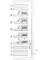
図6は、図2において、領域Bとして破線で囲んで示される引き出し配線とタッチパネルを動作させる集積回路(IC)が搭載された回路基板とを接続する実装領域を拡大した平面図であり、各引き出し配線の一部と実装端子とを示している。なお、実装端子とは、FPC(Flexible Printed Circuit)などを実装するための端子である。 FIG. 6 is an enlarged plan view of a mounting area for connecting a lead wiring shown by a dashed line as region B in FIG. 2 and a circuit board on which an integrated circuit (IC) for operating the touch panel is mounted. A part of lead-out wiring and a mounting terminal are shown. The mounting terminal is a terminal for mounting a flexible printed circuit (FPC) or the like.
図6においては、引き出し配線ER1〜ER6および最外シールド配線41と、引き出し配線EC6〜EC8とを示しており、引き出し配線ER1〜ER6および最外シールド配線41のそれぞれの端部は実装端子G100に接続され、引き出し配線EC6〜ER8のそれぞれの端部は実装端子G200に接続されている。そして、引き出し配線ER6〜ER2のそれぞれに接続される実装端子G100に間隔を開けて平行するように電位固定端子G1〜G5が配設されている。また、図7には、図6におけるD−D線での矢視方向断面の構成を示している。 In FIG. 6, the lead wires ER1 to ER6 and the
図6および図7に示されるように、電位固定端子G1〜G5と各実装端子G100との間には、引き出し配線ER2〜ER6のそれぞれに静電容量を付加するための付加容量50が設けられている。付加容量50では、実装端子に接続された櫛歯型の実装端子側電極502(第1の電極)と、電位固定端子に接続された櫛歯型の電位固定電極501(第2の電極)とが、互いの櫛歯が相手の櫛歯の間に入り込むように組み合わされており、互いの櫛歯部分の間に静電容量が形成されることとなる。なお、最外側引き出し配線となる引き出し配線ER1および最外シールド配線41については、付加容量50および電位固定端子を設けていない。 As shown in FIGS. 6 and 7,
ここで、電位固定電極501および実装端子側電極502の櫛歯部分の長さと電極間隔を調整することで静電容量を調整することができ、静電容量の微妙な調整が可能となる。 Here, the electrostatic capacitance can be adjusted by adjusting the length of the comb teeth portion of the
なお、付加容量50は上述した櫛歯型の電極形状に限定されるものではなく、直線状の電極、鈎型の電極など静電容量を形成できる形状であれば良い。 The
また、付加容量50に設定する容量値は、最外側引き出し配線となる引き出し配線ER1の静電容量と、それ以外の引き出し配線の静電容量との差に相当する値に設定され、例えば、引き出し配線ER1の静電容量と、その隣の引き出し配線ER2の静電容量との差に相当する値、または、引き出し配線ER1の静電容量と、引き出し配線ER2〜ER6における静電容量の平均値との差に相当する値などに設定することが考えられる。 The capacitance value set for the
電位固定端子G1〜G5は電位固定電極501の電位を固定するための端子であり、図7に示されるように、層間絶縁膜11を貫通する開口部OP2を介して図示されない配線に接続され、一定の電位、例えば接地電位に固定される。なお、各実装端子G100上には層間絶縁膜11を貫通する開口部OP1が設けられており、当該開口部OP1を介して図示されないICに接続される。 Potential fixing terminals G1 to G5 are terminals for fixing the potential of the
なお、図7に示されるように、電位固定電極501および実装端子側電極502は、実装端子G100および電位固定端子G1〜G5と同じ層に設けられるので、引き出し配線ER1〜ER6、実装端子G100および電位固定端子G1〜G5の形成工程と同じ工程で形成することができ、付加容量50を設けることによる製造工程の増加を抑制することができる。 As shown in FIG. 7, the
以上説明したように、最外側引き出し配線となる引き出し配線ER1以外の引き出し配線ER2〜ER6のそれぞれに対して、静電容量を付加するための付加容量50を設けることで、引き出し配線ER1とそれ以外の引き出し配線との間で発生していた静電容量の偏差を軽減することが可能となり、検出感度の低下を抑制できる。 As described above, by providing the
また、実装領域で静電容量の調整をするので、静電容量の調整領域を額縁領域に設ける場合に比べて、額縁領域を大きくする必要がないので、狭小な額縁への対応も可能となる。 In addition, since the capacitance is adjusted in the mounting area, it is not necessary to enlarge the frame area as compared to the case where the capacitance adjustment area is provided in the frame area, so it is possible to cope with a narrow frame. .
また、引き出し配線ER2〜ER6に付加する付加容量50における静電容量は全て同じとすることで、静電容量を個々に異なった値とする場合に比べて設計も含めた製造工程を簡略化できる。 Further, by making all the capacitances of the
なお、付加容量50の大きさは、例えば、電位固定端子と実装端子との間の長さで0.3mm程度、電位固定端子(および実装端子)の延在方向の長さで1.0mm程度となるように設定し、電位固定電極501および実装端子側電極502の配列間隔は3μm程度、それぞれの電極幅は3μm程度とすることが考えられる。 The size of the
<変形例1>
次に、図8を用いて、実施の形態1のタッチスクリーン1の変形例1の構成について説明する。なお、図8においては、図6を用いて説明した構成と同一の構成については同一の符号を付し、重複する説明は省略する。<
Next, the configuration of the
図8に示すように、本変形例1では、電位固定端子G1〜G5と各実装端子G100との間には、それぞれ静電容量が異なる付加容量51〜55が設けられている。すなわち、引き出し配線ER6の実装端子G100と電位固定端子G1との間には付加容量51が設けられ、引き出し配線ER5の実装端子G100と電位固定端子G2との間には付加容量52が設けられ、引き出し配線ER4の実装端子G100と電位固定端子G3との間には付加容量53が設けられ、引き出し配線ER3の実装端子G100と電位固定端子G4との間には付加容量54が設けられ、引き出し配線ER2の実装端子G100と電位固定端子G5との間には付加容量55が設けられている。 As shown in FIG. 8, in the first modification,
そして、付加容量51〜55における静電容量は、最外側引き出し配線となる引き出し配線ER1より遠ざかるに従い大きくなるように櫛歯型の電極の大きさが変更されている。すなわち、付加容量55の静電容量が最も小さく、付加容量51の静電容量が最も大きくなるように構成されている。これは、引き出し配線ER1より遠ざかるにつれて各引き出し配線の静電容量が小さくなっているためであり、その差を補うように付加容量51〜55における静電容量を設定する。これにより引き出し配線間の静電容量の偏差がより小さくなることで、検出感度の向上が可能となる。 The capacitances of the
<変形例2>
次に、図9を用いて、実施の形態1のタッチスクリーン1の変形例2の構成について説明する。なお、図9においては、図6を用いて説明した構成と同一の構成については同一の符号を付し、重複する説明は省略する。<Modification 2>
Next, the configuration of the modification 2 of the
図9に示すように、本変形例2では、各実装端子G100のそれぞれに電位固定端子を併設するのではなく、何れかの実装端子G100に平行して電位固定端子を設け、全ての電位固定電極は、当該電位固定端子に共通して接続される構成としている。 As shown in FIG. 9, in the second modification, potential fixing terminals are not provided for each mounting terminal G100, but potential fixing terminals are provided in parallel with any one of the mounting terminals G100 to fix all the potentials. The electrodes are commonly connected to the potential fixing terminal.
すなわち、図9の例では、引き出し配線ER6の実装端子G100と引き出し配線ER5の実装端子G100との間に電位固定端子G1を設け、引き出し配線ER6の実装端子G100と電位固定端子G1との間の付加容量50では、実装端子に実装端子側電極502が接続され、電位固定端子に電位固定電極501が接続された構成を採るが、それ以外の付加容量50では、実装端子に実装端子側電極502が接続され、電位固定電極501は導体パターンL100に共通に接続され、導体パターンL100は電位固定端子G1に接続された構成となっている。なお、構成上の違いから、引き出し配線ER6の実装端子G100と電位固定端子G1との間の付加容量50を第1の付加容量と呼称し、それ以外の付加容量50を第2の付加容量と呼称する場合もある。 That is, in the example of FIG. 9, the potential fixing terminal G1 is provided between the mounting terminal G100 of the lead wire ER6 and the mounting terminal G100 of the lead wire ER5, and the portion between the mounting terminal G100 of the lead wire ER6 and the potential fixing terminal G1 is provided. In the
導体パターンL100は、電位固定電極501および実装端子側電極502と同じ層に設けられ、電位固定電極501および実装端子側電極502の形成工程と同じ工程で形成することができる。 The conductor pattern L100 is provided in the same layer as the potential fixed
以上説明したように、各実装端子G100のそれぞれに電位固定端子を併設するのではなく、何れかの実装端子G100に併設し、全ての電位固定電極は、当該電位固定端子に共通して接続される構成とすることで電位固定電極を集約でき、実装端子数が削減されることで、タッチスクリーン1と回路基板(図示されず)とを接続するFPCの幅縮小によるコスト削減が可能となる。 As described above, the potential fixing terminals are not provided separately for each mounting terminal G100, but are provided for any mounting terminal G100, and all potential fixing electrodes are commonly connected to the potential fixing terminals. With this configuration, the potential fixed electrodes can be integrated, and the number of mounting terminals can be reduced, whereby cost reduction can be achieved by reducing the width of the FPC connecting the
なお、電位固定電極を集約することでFPCの端子間隔(端子ピッチ)を1間隔当たり0.2〜0.5mm程度縮小することができ、FPC全体では十数mmの幅縮小が期待できる。 Note that by consolidating the potential fixed electrodes, the terminal spacing (terminal pitch) of the FPC can be reduced by about 0.2 to 0.5 mm per spacing, and a reduction in width of a dozen or so mm can be expected in the entire FPC.
<変形例3>
次に、図10を用いて、実施の形態1のタッチスクリーン1の変形例3の構成について説明する。なお、図10においては、図8および図9を用いて説明した構成と同一の構成については同一の符号を付し、重複する説明は省略する。<Modification 3>
Next, the configuration of the third modification of the
図10に示すように、本変形例3では、図8を用いて説明した変形例1と同様に、付加容量51〜55における静電容量は、最外側引き出し配線となる引き出し配線ER1より遠ざかるに従い大きくなるように櫛歯型の電極の大きさが変更されている。そして、図9を用いて説明した変形例2と同様に、各実装端子G100のそれぞれに電位固定端子を併設するのではなく、引き出し配線ER6の実装端子G100と引き出し配線ER5の実装端子G100との間に電位固定端子G1を設け、引き出し配線ER6の実装端子G100と電位固定端子G1との間の付加容量51では、実装端子に実装端子側電極502が接続され、電位固定端子に電位固定電極501が接続された構成を採るが、付加容量52〜55では、実装端子に実装端子側電極502が接続され、電位固定電極501は導体パターンL100に共通に接続され、導体パターンL100は電位固定端子G1に接続された構成となっている。 As shown in FIG. 10, in the third modification, as in the first modification described with reference to FIG. 8, the capacitances of the
ここで、引き出し配線ER1より遠ざかるにつれて各引き出し配線の静電容量が小さくなっており、その差を補うように付加容量51〜55における静電容量が設定されており、これによって、引き出し配線間の静電容量の偏差がより小さくなることで、検出感度の向上が可能となる。また、電位固定電極を集約することで、実装端子数が削減され、タッチスクリーン1と回路基板(図示されず)とを接続するFPCの幅縮小によるコスト削減が可能となる。 Here, as the distance from the lead wire ER1 increases, the capacitances of the lead wires decrease, and the capacitances of the
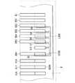
<実施の形態2>
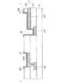
図2、図11および図12を用いて、実施の形態2のタッチスクリーン1の構成について説明する。図11は、図2において、領域Bとして破線で囲んで示される引き出し配線と、タッチパネルを動作させるICが搭載された回路基板とを接続する実装領域を拡大した平面図であり、各引き出し配線の一部と実装端子とを示している。図12には、図11におけるE−E線での矢視方向断面の構成を示している。Second Embodiment
The configuration of the
図11においては、引き出し配線ER1〜ER6および最外シールド配線41と、引き出し配線EC6〜EC8とを示しており、引き出し配線ER1〜ER6および最外シールド配線41のそれぞれの端部は実装端子G100に接続され、引き出し配線EC6〜ER8のそれぞれの端部は実装端子G200に接続されている。そして、引き出し配線ER6〜ER2のそれぞれに接続される実装端子G100には、その下方において実装端子G100の延在方向に沿うように、引き出し配線ER2〜ER6のそれぞれに静電容量を付加するための電位固定電極201が設けられている。なお、電位固定電極201が設けられた領域が付加容量56となるが、最外側引き出し配線となる引き出し配線ER1および最外シールド配線41については、付加容量56を設けていない。 In FIG. 11, the lead wires ER1 to ER6 and the
そして、引き出し配線ER6の実装端子G100と引き出し配線ER5の実装端子G100との間には電位固定電極201と同層に形成された電位固定端子G10が設けられており、引き出し配線ER2〜ER6のそれぞれの下方の電位固定電極201は、導体パターンL200に共通に接続され、導体パターンL200は電位固定電極201に接続された構成となっている。なお、層間絶縁膜11は透明な絶縁膜で構成されているので、電位固定電極201および導体パターンL200は視認することができる。 A potential fixed terminal G10 formed in the same layer as the potential fixed
図12に示されるように、本実施の形態2では、層間絶縁膜11は、透明基板10上に下層膜111および上層膜112をこの順に積層した積層膜で構成されており、上層膜112中に実装端子G100を含む引き出し配線ER1〜ER6および最外シールド配線41が形成され、電位固定電極201、導体パターンL200および電位固定端子G10は下層膜111中に形成されている。 As shown in FIG. 12, in the second embodiment, the
図12に示されるように、実装端子G100と電位固定電極201とが上下において重なる部分に静電容量が形成されることとなる。この場合、実装端子G100と電位固定電極201とが重なり合う部分の面積を調整することで、静電容量を調整することができる。 As shown in FIG. 12, a capacitance is formed in the portion where the mounting terminal G100 and the potential fixed
なお、電位固定端子G10上には上層膜112および下層膜111を貫通する開口部OP4が設けられており、電位固定端子G10は開口部OP4を介して図示されない配線に接続され、一定の電位、例えば接地電位に固定される。また、各実装端子G100上には上層膜112を貫通する開口部OP3が設けられており、当該開口部OP3を介して図示されないICに接続される。 Note that an opening OP4 penetrating the
以上説明したように、最外側引き出し配線となる引き出し配線ER1以外の引き出し配線ER2〜ER6のそれぞれに対して、静電容量を付加するための付加容量56を設けることで、引き出し配線ER1とそれ以外の引き出し配線との間で発生していた静電容量の偏差を軽減することが可能となり、検出感度の低下を抑制できる。 As described above, by providing the
また、実装領域で静電容量の調整をするので、静電容量の調整領域を額縁領域に設ける場合に比べて、額縁領域を大きくする必要がないので、狭小な額縁への対応も可能となる。 In addition, since the capacitance is adjusted in the mounting area, it is not necessary to enlarge the frame area as compared to the case where the capacitance adjustment area is provided in the frame area, so it is possible to cope with a narrow frame. .
また、引き出し配線ER2〜ER6に付加する付加容量56における静電容量は全て同じとすることで、静電容量を個々に異なった値とする場合に比べて設計も含めた製造工程を簡略化できる。 Further, by making all the capacitances of the
また、実装端子G100と電位固定電極201とを上下において重ねることで付加容量56を形成するので静電容量を形成するための領域を小さくでき、また、電位固定電極を集約することで、実装端子数が削減され、タッチスクリーン1と回路基板(図示されず)とを接続するFPCの幅縮小によるコスト削減が可能となる。なお、本実施の形態2の構成を採る場合、FPCの端子間隔(端子ピッチ)を0.1mm程度まで狭くすることが可能となる。 Further, the
<変形例1>
次に、図13を用いて、実施の形態2のタッチスクリーン1の変形例1の構成について説明する。なお、図13においては、図11を用いて説明した構成と同一の構成については同一の符号を付し、重複する説明は省略する。<
Next, the configuration of the
図13に示すように、本変形例1では、各実装端子G100には、それぞれ静電容量が異なる付加容量56〜60が設けられている。すなわち、引き出し配線ER6の実装端子G100には付加容量56が設けられ、引き出し配線ER5の実装端子G100には付加容量57が設けられ、引き出し配線ER4の実装端子G100には付加容量58が設けられ、引き出し配線ER3の実装端子G100には付加容量59が設けられ、引き出し配線ER2の実装端子G100には付加容量60が設けられている。 As shown in FIG. 13, in the first modification, each mounting terminal G100 is provided with
そして、付加容量56〜60における静電容量は、最外側引き出し配線となる引き出し配線ER1より遠ざかるに従い大きくなるように電位固定電極201の長さが変更されている。すなわち、付加容量56の静電容量が最も大きく、付加容量60の静電容量が最も小さくなるように電位固定電極201の長さが調整されている。 The length of the potential fixed
ここで、引き出し配線ER1より遠ざかるにつれて各引き出し配線の静電容量が小さくなっており、その差を補うように付加容量56〜60における静電容量が設定されており、これによって引き出し配線間の静電容量の偏差がより小さくなることで、検出感度の向上が可能となる。 Here, as the distance from the lead wire ER1 increases, the capacitances of the lead wires decrease, and the capacitances of the
<変形例2>
次に、図14および図15を用いて、実施の形態2のタッチスクリーン1の変形例2の構成について説明する。図15には、図14におけるF−F線での矢視方向断面の構成を示している。なお、図14および図15においては、図12および図13を用いて説明した構成と同一の構成については同一の符号を付し、重複する説明は省略する。<Modification 2>
Next, the configuration of the modification 2 of the
図14に示すように、本変形例2では、図13を用いて説明した変形例1と同様に、各実装端子G100には、それぞれ静電容量が異なる付加容量56〜60が設けられており、付加容量56〜60における静電容量は、最外側引き出し配線となる引き出し配線ER1より遠ざかるに従い大きくなるように電位固定電極201の長さが調整されている。 As shown in FIG. 14, in the second modification, as in the first modification described with reference to FIG. 13,
そして、引き出し配線ER6の実装端子G100と引き出し配線ER5の実装端子G100との間には電位固定電極201と同層に形成された電位固定端子G10が設けられており、引き出し配線ER2〜ER6のそれぞれの下方の電位固定電極201は、導体パターンL200に共通に接続され、導体パターンL200は電位固定電極201に接続された構成となっているが、図15に示されるように、電位固定端子G10の一部に重なるように、上層膜112中に上部電位固定端子G20が配設されている。 A potential fixed terminal G10 formed in the same layer as the potential fixed
電位固定端子G10上には上層膜112および下層膜111を貫通するコンタクトホールCH1が設けられており、また、電位固定端子G1上には上層膜112を貫通する開口部OP6が設けられている。そして、コンタクトホールCH1内および開口部OP6内は上層膜112に形成された導電膜81によって覆われ、電位固定端子G10と上部電位固定端子G20とは導電膜81で電気的に接続される。この導電膜81は、電位固定端子G10の電位を固定する配線となる。 A contact hole CH1 penetrating the
また、各実装端子G100上には上層膜112を貫通する開口部OP5が設けられており、当該開口部OP3内は導電膜82で覆われ、導電膜82を介して図示されないICに接続される。ここで、導電膜81および82は、ITO(Indium Tin Oxide)などの透明配線材料、またはアルミニウム、銅などの金属配線材料で構成されている。なお、引き出し配線ER1〜ER6、EC1〜EC8、電位固定端子G1〜G5、G10、上部電位固定端子G20および実装端子G100はアルミニウム系の金属配線材料、または、クロム、銅、銀等の合金、またはこれらの合金上にアルミニウム等を積層した多層金属配線材料で構成されている。 Further, an opening OP5 penetrating the
このような構成を採ることで、電位固定端子G10はコンタクトホールCH1および開口部OP6を介して電位固定されることになるので、電位固定端子G10を上層膜112上の配線に直接接続する構成に比べて段差の違いによる実装不良が改善され歩留り向上によるコスト差削減が期待できる。 By adopting such a configuration, potential fixing terminal G10 is fixed in potential via contact hole CH1 and opening OP6, so that potential fixing terminal G10 is directly connected to the wiring on
また、各付加容量の静電容量は、引き出し配線間の静電容量の偏差をより小さくするように設定されており、引き出し配線間の静電容量の偏差がより小さくなることで、検出感度の向上が可能となる。また、電位固定電極を集約することで、実装端子数が削減され、タッチスクリーン1と回路基板(図示されず)とを接続するFPCの幅縮小によるコスト削減が可能となる。 Further, the capacitance of each additional capacitance is set so as to make the deviation of the capacitance between the lead-out lines smaller, and the deviation of the capacitance between the lead-out lines becomes smaller. It is possible to improve. Further, by consolidating the potential fixed electrodes, the number of mounting terminals can be reduced, and cost reduction can be achieved by reducing the width of the FPC connecting the
<比較例との効果の相違>
以上説明した実施の形態1および2においては、行方向配線21に接続される引き出し配線ER1〜ER6において、引き出し配線ER1とそれ以外の引き出し配線との間で発生していた静電容量の偏差を軽減する構成について説明したが、列方向配線31に接続される引き出し配線CR1〜CR8においても、引き出し配線CR1とそれ以外の引き出し配線との間で静電容量の偏差が発生する可能性はあるので、引き出し配線CR2〜CR8にも、静電容量の偏差を軽減する構成、すなわち、付加容量により静電容量の調整を行う構成を設けても良い。以下、行方向配線および列方向配線の引き出し配線において付加容量により静電容量の調整を行う構成を設けた場合の効果の一例について説明する。<Differences in effect from comparative example>
In the first and second embodiments described above, in the lead wirings ER1 to ER6 connected to the
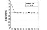
効果を確認するため、10本の行方向配線R1〜R10と14本の列方向配線C1〜14とを備えたタッチスクリーンを、導電性を有しかつ接地されるフロントフレームを備えた液晶ディスプレイに装着したサンプルを作製し、タッチスクリーンの各配線の相互容量を測定した。 In order to confirm the effect, a touch screen provided with ten row directional wirings R1 to R10 and fourteen column directional wirings C1 to 14 is used as a liquid crystal display provided with a conductive and grounded front frame. The mounted sample was prepared and the mutual capacitance of each wire of the touch screen was measured.
なお、付加容量による静電容量の調整を行わない従来的なタッチスクリーンのサンプルも同様に作製し、比較例とした。 In addition, the sample of the conventional touch screen which does not perform adjustment of the electrostatic capacitance by additional capacitance was similarly produced, and it was set as the comparative example.
図16は、比較例と実施の形態1によるタッチスクリーンにおける、行方向配線R1〜R10の自己容量相対値を示している。なお自己容量相対値は、比較例によるタッチスクリーンの行方向配線R5の自己容量を1とした場合の相対値を表している。 FIG. 16 shows relative values of self-capacitance of row-direction wirings R1 to R10 in the touch screen according to the comparative example and the first embodiment. The self-capacitance relative value represents a relative value when the self-capacitance of the row-direction wiring R5 in the comparative example is 1.
図16に示すように、比較例では、行方向配線R2〜R10の自己容量相対値が何れも1程度とほぼ揃っているが、最外側の行方向配線R1の自己容量相対値が1.5程度となっておりオフセットしている。一方、実施の形態1によるタッチスクリーンでは、最外となる行方向配線R1を含め、全ての行方向配線の自己容量相対値が1程度でほぼ揃っていることが判る。 As shown in FIG. 16, in the comparative example, the relative values of self-capacitance of row direction wirings R2 to R10 are substantially equal to about 1, but the relative value of self-capacitance of outermost row direction wiring R1 is 1.5. It has become an extent and offset. On the other hand, in the touch screen according to the first embodiment, it is understood that the self-capacitance relative values of all the row directional wirings are substantially equal at about 1, including the outermost row directional wiring R1.
図17は、比較例と実施の形態1と同様の静電容量の偏差を軽減する構成を列方向配線の引き出し配線に設けたタッチスクリーンにおける、列方向配線C1〜C14の自己容量相対値を示す。なお自己容量相対値は、比較例によるタッチスクリーンの列方向配線C7の自己容量を1とした場合の相対値を表している。 FIG. 17 shows relative values of self-capacitance of column-direction wires C1 to C14 in a touch screen provided with a configuration similar to that of the comparative example and the first embodiment in which the deviation of electrostatic capacitance is reduced in the lead-out wires of the column-direction wires. . The self-capacitance relative value represents a relative value when the self-capacitance of the column-direction wiring C7 of the comparative example is 1.
図17に示すように、比較例では、列方向配線C2〜C14の自己容量相対値が何れも1程度とほぼ揃っているが、最外側の列方向配線C1の自己容量相対値が1.3程度となっておりオフセットしている。一方、静電容量の偏差を軽減する構成を設けたタッチスクリーンでは、最外側の列方向配線C1を含め、全ての列方向配線の自己容量相対値が何れも1程度とほぼ揃っていることが判る。 As shown in FIG. 17, in the comparative example, the relative self-capacitance values of the column-direction wires C2 to C14 are substantially equal to about 1, but the relative self-capacitance value of the outermost column-direction wire C1 is 1.3. It has become an extent and offset. On the other hand, in the touch screen provided with a configuration for reducing the capacitance deviation, the self-capacitance relative values of all the column-direction wirings including the outermost column-direction wiring C1 are almost equal to about one. I understand.
また、以上の説明においては最外側引き出し配線となる引き出し配線ER1およびCR1と、それ以外の引き出し配線との間で静電容量の偏差について説明したが、表示装置の大型化に伴い最外側引き出し配線だけでなく、さらに内側の引き出し配線と、それ以外の引き出し配線との間で静電容量の偏差が生じる場合も想定され、その場合は、最外側引き出し配線と、さらに内側の幾本かの引き出し配線についても付加容量を与えない構成とする。 Further, in the above description, the deviation of the electrostatic capacitance is described between the lead wirings ER1 and CR1 serving as the outermost lead wirings and the other lead wirings, but the outermost lead wirings are accompanied by the enlargement of the display device. Not only is it also assumed that capacitance deviation occurs between the inner lead wire and the other lead wires, in which case the outermost lead wire and some inner leads are drawn. No additional capacitance is given to the wiring.
<実施の形態3>
図18は、本発明に係る実施の形態3のタッチパネル70の構成を模式的に示す平面図である。タッチパネル70は、図1に示した実施の形態1のタッチスクリーン1と、フレキシブルプリント基板71(FPC)と、コントローラ基板72とを備えている。Embodiment 3
FIG. 18 is a plan view schematically showing the configuration of the
このフレキシブルプリント基板71を介して、タッチスクリーン1の行方向配線21および列方向配線31の端部と、コントローラ基板72とが電気的に接続されることによって、タッチスクリーン1は、タッチパネル70の主要構成要素として機能する。 By electrically connecting the ends of the row
コントローラ基板72には、タッチ位置検出処理回路73が搭載されている。タッチ位置検出処理回路73は、信号電圧の印加によって指示体との間に形成される静電容量で構成されるタッチ容量の検出と、検出結果に基づいて、指示体のタッチ位置のタッチスクリーン1上におけるタッチ位置の算出処理を行う。また、コントローラ基板72は、タッチ位置検出処理回路73で算出されたタッチ位置を、外部の処理装置に出力するための外部接続端子74を備えている。 The touch position
以上のように、本実施の形態3によれば、タッチパネル70が実施の形態1のタッチスクリーン1を備えることによって、タッチスクリーン1の最外の引き出し配線と、LCDなどの表示モジュールの間に生じるカップリングが低減され、カップリングに起因するセンサキャパシタの静電容量のオフセットが抑制されて、静電容量検出感度の偏りが低減されたタッチパネル70を得ることができる。 As described above, according to the third embodiment, when the
なお、上記では、実施の形態1のタッチスクリーンを用いる場合について説明したが、これに限るものではなく、実施の形態2のタッチスクリーンを用いる場合であっても同様の効果が得られる。 Although the case where the touch screen of the first embodiment is used is described above, the present invention is not limited to this, and the same effect can be obtained even when the touch screen of the second embodiment is used.
<実施の形態4>
本発明の第4の実の形態である表示装置は、前述の図18に示すタッチパネル70と、情報を表示可能なLCDなどの表示モジュールとを備えることを特徴としている。タッチパネル70は、表示モジュールの表示画面よりも使用者側に配置される。換言すれば、表示モジュールは、タッチパネル70のタッチスクリーンに対して指示する側とは反対側に配置される。このような構成とすることによって、使用者が指示したタッチ位置を検出する機能を有するタッチパネル付きの表示装置を得る。Fourth Preferred Embodiment
A display device according to a fourth embodiment of the present invention is characterized by including the
このように、本実施の形態の表示装置によれば、静電容量検出感度の偏りが低減されたタッチパネル70を備えており、静電容量検出感度の偏りが低減されたタッチパネル付きの表示装置を得ることができる。 As described above, according to the display device of the present embodiment, the display device with the touch panel is provided with the
<実施の形態5>
本発明に係る実施の形態5の電子機器は、実施の形態3のタッチパネル70(図18)と、LCDなどの表示モジュールと、電子装置である図示されない信号処理装置(電子処理部)とを備えることを特徴としている。The Fifth Preferred Embodiment
The electronic device of the fifth embodiment according to the present invention includes the touch panel 70 (FIG. 18) of the third embodiment, a display module such as an LCD, and a signal processing device (electronic processing unit) not shown which is an electronic device. It is characterized by
信号処理装置は、タッチパネル70の外部接続端子74から出力された信号を入力し、デジタル信号として出力する。すなわち、信号処理装置は、タッチパネル70のタッチ位置検出処理回路73で検出されたタッチ位置の情報に対して予め定められた処理を電子的に行う。このように、信号処理装置をタッチパネル70に接続する構成とすることによって、タッチパネル70のタッチ位置検出処理回路73で検出されたタッチ位置の情報をコンピュータなどの外部信号処理装置に出力する、デジタイザなどのタッチ位置検出機能付き電子機器を得ることができる。 The signal processing apparatus receives a signal output from the
なお、信号処理装置は、タッチパネル70のコントローラ基板72に内蔵(搭載)されても良い。この場合、信号処理装置が、USB(Universal Serial Bus)のようなバス規格を満たすような出力機能を備えることによって、汎用性の高いタッチ位置検出機能付き電子機器を実現することができる。 The signal processing device may be built in (mounted) on the
以上のように、本実施の形態の電子機器によれば、静電容量検出感度の偏りが低減されたタッチパネル70を備えており、静電容量検出感度の偏りが低減された、投影型静電容量方式のタッチ位置検出機能付き電子機器を得ることができる。 As described above, the electronic device according to the present embodiment includes the
なお、本発明は、その発明の範囲内において、各実施の形態を自由に組み合わせたり、各実施の形態を適宜、変形、省略することが可能である。 In the present invention, within the scope of the invention, each embodiment can be freely combined, or each embodiment can be appropriately modified or omitted.
1 タッチスクリーン、21 行方向配線、31 列方向配線、50〜56 付加容量、501 電位固定電極、502 実装端子側電極、G1〜G5,G10 電位固定端子、G20 上部電位固定端子、L100,L200 導体パターン。 1 Touch screen, 21 row direction wiring, 31 column direction wiring, 50 to 56 additional capacitance, 501 potential fixed electrode, 502 mounting terminal side electrode, G1 to G5, G10 potential fixed terminal, G20 upper potential fixed terminal, L100, L200 conductor pattern.
Claims (11)
Translated fromJapanese前記列方向配線および前記行方向配線に接続された複数の引き出し配線のそれぞれの実装端子が配置された実装領域に設けられた、前記複数の引き出し配線に静電容量を付加するための付加容量と、前記付加容量の一方の電極の電位を固定する少なくとも1つの電位固定端子と、を備えるタッチスクリーン。A column direction wiring extending in a column direction and a row direction wiring extending in a row direction orthogonal to the column direction are provided, and a region where the column direction wiring and the row direction wiring intersect in a three-dimensional manner is detected The touch screen is a cell, and
An additional capacitance for adding electrostatic capacitance to the plurality of lead wirings provided in a mounting area where the mounting terminals of the plurality of lead wirings connected to the column direction wiring and the row direction wiring are arranged A touch screen including at least one potential fixing terminal for fixing the potential of one electrode of the additional capacitance.
前記複数の引き出し配線のうち、最も外側に配置される最外側引き出し配線以外の引き出し配線に付加され、その値は、前記最外側引き出し配線と前記最外側引き出し配線以外の引き出し配線との間の静電容量の差に相当する値に設定される、請求項1記載のタッチスクリーン。The additional capacity is
Among the plurality of lead wires, the lead wire is added to the lead wire other than the outermost lead wire disposed on the outermost side, and the value is added to the distance between the outermost lead wire and the lead wire other than the outermost lead wire. The touch screen according to claim 1, wherein the touch screen is set to a value corresponding to a difference in capacitance.
前記最外側引き出し配線以外の引き出し配線の全てについて同じに設定される、請求項2記載のタッチスクリーン。The capacitance of the additional capacitance is
The touch screen according to claim 2, wherein the touch screen is set to be the same for all of the lead wirings other than the outermost lead wiring.
前記最外側引き出し配線から遠ざかるに従い大きくなるように設定される、請求項2記載のタッチスクリーン。The capacitance of the additional capacitance is
The touch screen as set forth in claim 2, wherein the touch screen is set to become larger as it goes away from the outermost lead wire.
前記複数の引き出し配線のそれぞれの実装端子の間に前記実装端子と同層に複数設けられた電位固定端子であって、
前記付加容量は、
前記実装端子に接続された第1の電極と、
前記電位固定端子に接続された第2の電極と、を有する、請求項2から請求項4の何れか1項に記載のタッチスクリーン。The at least one potential fixed terminal is
A plurality of potential fixing terminals provided in the same layer as the mounting terminal between the mounting terminals of the plurality of lead wirings,
The additional capacity is
A first electrode connected to the mounting terminal;
The touch screen according to any one of claims 2 to 4, further comprising: a second electrode connected to the potential fixing terminal.
前記複数の引き出し配線の何れか1つの実装端子間に前記実装端子と同層に設けられた電位固定端子であって、
前記付加容量は、
前記実装端子に接続された第1の電極と、前記電位固定端子に接続された第2の電極と、を有した第1の付加容量と、
前記実装端子に接続された第1の電極と、前記電位固定端子に接続された導体パターンに接続された第2の電極と、を有した第2の付加容量と、を含む、請求項2から請求項4の何れか1項に記載のタッチスクリーン。The at least one potential fixed terminal is
A potential fixed terminal provided in the same layer as the mounting terminal between any one mounting terminal of the plurality of lead wirings,
The additional capacity is
A first additional capacitance having a first electrode connected to the mounting terminal and a second electrode connected to the potential fixing terminal;
The second additional capacitance includes a first electrode connected to the mounting terminal and a second electrode connected to a conductor pattern connected to the potential fixing terminal. A touch screen as claimed in any one of the preceding claims.
前記複数の引き出し配線の何れか1つの実装端子間に前記実装端子より下層に設けられた電位固定端子であって、
前記付加容量は、
前記実装端子を第1の電極とし、
前記実装端子の下方に設けられ、前記電位固定端子と同層の電位固定電極を第2の電極とし、
前記第2の電極は、前記電位固定端子と同層で前記電位固定端子に接続された導体パターンに接続され、
前記第1の電極と前記第2の電極とが上下において重なる部分に静電容量が形成される、請求項2から請求項4の何れか1項に記載のタッチスクリーン。The at least one potential fixed terminal is
It is a potential fixed terminal provided below the mounting terminal between any one mounting terminal of the plurality of lead wirings,
The additional capacity is
The mounting terminal is a first electrode,
The potential fixing electrode provided on the lower side of the mounting terminal and in the same layer as the potential fixing terminal is used as a second electrode,
The second electrode is connected to a conductor pattern connected to the potential fixing terminal in the same layer as the potential fixing terminal,
The touch screen according to any one of claims 2 to 4, wherein a capacitance is formed in a portion where the first electrode and the second electrode overlap in the upper and lower direction.
前記電位固定端子の上方に設けられ、前記実装端子と同層の上部電位固定端子をさらに備え、
前記電位固定端子は、前記上部電位固定端子に電気的に接続される、請求項7記載のタッチスクリーン。The touch screen is
It further comprises an upper potential fixing terminal provided on the upper side of the potential fixing terminal and in the same layer as the mounting terminal,
The touch screen according to claim 7, wherein the potential fixing terminal is electrically connected to the upper potential fixing terminal.
前記タッチスクリーンに対して指示する指示体と、前記行方向配線および前記列方向配線との間の静電容量に基づいて、前記指示体によって指示された前記タッチスクリーン上の位置を検出するタッチ位置検出回路と、を備える、タッチパネル。A touch screen according to any one of claims 1 to 8;
A touch position for detecting a position on the touch screen instructed by the indicator based on an electrostatic capacitance between the indicator instructing the touch screen, the row directional wiring and the column directional wiring And a detection circuit.
前記タッチパネルの前記タッチスクリーンに対して指示する側とは反対側に配置され、情報を表示可能な表示モジュールと、を備える、表示装置。A touch panel according to claim 9;
A display module disposed on the side opposite to the side for instructing the touch screen of the touch panel and capable of displaying information.
前記タッチパネルの前記タッチ位置検出回路で検出された前記位置の情報に対して予め定められた処理を電子的に行う電子処理部と、を備える、電子機器。A touch panel according to claim 9;
An electronic processing unit which electronically performs a predetermined process on information of the position detected by the touch position detection circuit of the touch panel.
Priority Applications (2)
| Application Number | Priority Date | Filing Date | Title |
|---|---|---|---|
| JP2015219262AJP6545083B2 (en) | 2015-11-09 | 2015-11-09 | Touch screen, touch panel, display device and electronic device |
| US15/343,770US10303298B2 (en) | 2015-11-09 | 2016-11-04 | Touch screen, touch panel, display device, and electronic device |
Applications Claiming Priority (1)
| Application Number | Priority Date | Filing Date | Title |
|---|---|---|---|
| JP2015219262AJP6545083B2 (en) | 2015-11-09 | 2015-11-09 | Touch screen, touch panel, display device and electronic device |
Publications (2)
| Publication Number | Publication Date |
|---|---|
| JP2017091135A JP2017091135A (en) | 2017-05-25 |
| JP6545083B2true JP6545083B2 (en) | 2019-07-17 |
Family
ID=58667656
Family Applications (1)
| Application Number | Title | Priority Date | Filing Date |
|---|---|---|---|
| JP2015219262AActiveJP6545083B2 (en) | 2015-11-09 | 2015-11-09 | Touch screen, touch panel, display device and electronic device |
Country Status (2)
| Country | Link |
|---|---|
| US (1) | US10303298B2 (en) |
| JP (1) | JP6545083B2 (en) |
Cited By (1)
| Publication number | Priority date | Publication date | Assignee | Title |
|---|---|---|---|---|
| US11822744B2 (en) | 2021-03-30 | 2023-11-21 | Samsung Display Co., Ltd. | Display device |
Families Citing this family (13)
| Publication number | Priority date | Publication date | Assignee | Title |
|---|---|---|---|---|
| KR102424289B1 (en)* | 2017-06-01 | 2022-07-25 | 엘지디스플레이 주식회사 | Touch display device and panel |
| CN109144333A (en)* | 2017-06-15 | 2019-01-04 | 上海峰宁信息科技股份有限公司 | A kind of method that the realization of metal mesh opening touch control film electronic blackboard is bonded entirely |
| JP6906397B2 (en)* | 2017-08-10 | 2021-07-21 | 株式会社ジャパンディスプレイ | Display device |
| CN111133407B (en) | 2017-10-03 | 2023-08-15 | 株式会社和冠 | Sensor panel for detecting pen signals sent by a pen |
| JP7051386B2 (en)* | 2017-11-17 | 2022-04-11 | 株式会社デンソーテン | Circuit board |
| CN111316213B (en)* | 2017-12-13 | 2023-11-17 | 富士胶片株式会社 | Conductive components, touch panels and display devices |
| KR102427303B1 (en) | 2018-09-10 | 2022-08-01 | 삼성디스플레이 주식회사 | Display device |
| KR102600934B1 (en)* | 2018-11-23 | 2023-11-10 | 엘지디스플레이 주식회사 | Touch display panel and touch display device |
| JP7202906B2 (en)* | 2019-01-25 | 2023-01-12 | 株式会社ワコム | Sensor panel for detecting pen signals sent by the pen |
| JP7463636B2 (en)* | 2020-08-17 | 2024-04-09 | シャープ株式会社 | Touch Panel and Display Device |
| CN112035013B (en)* | 2020-08-31 | 2024-04-09 | 京东方科技集团股份有限公司 | Touch panel and manufacturing method thereof, and display device |
| CN114155804B (en)* | 2021-12-16 | 2023-09-19 | 合肥维信诺科技有限公司 | Display panel and display device |
| CN117850626B (en)* | 2024-03-04 | 2024-05-28 | 深圳市坤巨实业有限公司 | Capacitive touch display for solving interference of three-ground suspension system |
Family Cites Families (8)
| Publication number | Priority date | Publication date | Assignee | Title |
|---|---|---|---|---|
| GB9406702D0 (en) | 1994-04-05 | 1994-05-25 | Binstead Ronald P | Multiple input proximity detector and touchpad system |
| US6288707B1 (en)* | 1996-07-29 | 2001-09-11 | Harald Philipp | Capacitive position sensor |
| US6452514B1 (en) | 1999-01-26 | 2002-09-17 | Harald Philipp | Capacitive sensor and array |
| KR20070054825A (en)* | 2005-11-24 | 2007-05-30 | 엘지이노텍 주식회사 | Lighting device using LED |
| JP5106471B2 (en)* | 2009-04-24 | 2012-12-26 | 三菱電機株式会社 | Touch panel and display device including the same |
| JP5647864B2 (en)* | 2010-11-05 | 2015-01-07 | 富士フイルム株式会社 | Touch panel |
| US8910104B2 (en)* | 2012-01-23 | 2014-12-09 | Cirque Corporation | Graduated routing for routing electrodes coupled to touch sensor electrodes to thereby balance capacitance on the touch sensor electrodes |
| JP6456230B2 (en)* | 2015-04-21 | 2019-01-23 | 三菱電機株式会社 | Touch screen, touch panel, display device and electronic device |
- 2015
- 2015-11-09JPJP2015219262Apatent/JP6545083B2/enactiveActive
- 2016
- 2016-11-04USUS15/343,770patent/US10303298B2/enactiveActive
Cited By (1)
| Publication number | Priority date | Publication date | Assignee | Title |
|---|---|---|---|---|
| US11822744B2 (en) | 2021-03-30 | 2023-11-21 | Samsung Display Co., Ltd. | Display device |
Also Published As
| Publication number | Publication date |
|---|---|
| US10303298B2 (en) | 2019-05-28 |
| JP2017091135A (en) | 2017-05-25 |
| US20170131842A1 (en) | 2017-05-11 |
Similar Documents
| Publication | Publication Date | Title |
|---|---|---|
| JP6545083B2 (en) | Touch screen, touch panel, display device and electronic device | |
| JP6456230B2 (en) | Touch screen, touch panel, display device and electronic device | |
| JP6541418B2 (en) | Touch screen, touch panel, display device and electronic device | |
| JP6430062B2 (en) | Touch screen, touch panel, display device and electronic device | |
| JP6562706B2 (en) | Surface device, touch screen and liquid crystal display device | |
| US10359890B2 (en) | Touch screen, touch panel, and display apparatus | |
| US9760229B2 (en) | Touch screen, touch panel, display, and electronic equipment | |
| JP6562720B2 (en) | Touch screen, touch panel, display device and electronic device | |
| US9760230B2 (en) | Touch screen, touch panel, display device, and electronic device | |
| KR102281616B1 (en) | Touch screen panel and method of manufacturing the same | |
| JP5870945B2 (en) | Touch screen, touch panel, display device and electronic device | |
| JP6333042B2 (en) | Touch screen, touch panel, display device and electronic device | |
| JP2015210554A (en) | Touch screen, touch panel, display device, and electronic apparatus | |
| JP2023037375A (en) | Sensor module and display device including sensor module | |
| JP2020149563A (en) | Touch screens, touch panels, display devices and electronic devices | |
| JP2020024592A (en) | Touch screen, touch panel, display device, and electronic device | |
| JP6576080B2 (en) | Capacitive touch panel | |
| CN119024986A (en) | Sensor module, sensor device and display device having the same |
Legal Events
| Date | Code | Title | Description |
|---|---|---|---|
| A621 | Written request for application examination | Free format text:JAPANESE INTERMEDIATE CODE: A621 Effective date:20181010 | |
| A977 | Report on retrieval | Free format text:JAPANESE INTERMEDIATE CODE: A971007 Effective date:20190426 | |
| TRDD | Decision of grant or rejection written | ||
| A01 | Written decision to grant a patent or to grant a registration (utility model) | Free format text:JAPANESE INTERMEDIATE CODE: A01 Effective date:20190521 | |
| A61 | First payment of annual fees (during grant procedure) | Free format text:JAPANESE INTERMEDIATE CODE: A61 Effective date:20190618 | |
| R150 | Certificate of patent or registration of utility model | Ref document number:6545083 Country of ref document:JP Free format text:JAPANESE INTERMEDIATE CODE: R150 | |
| R250 | Receipt of annual fees | Free format text:JAPANESE INTERMEDIATE CODE: R250 | |
| R250 | Receipt of annual fees | Free format text:JAPANESE INTERMEDIATE CODE: R250 | |
| R250 | Receipt of annual fees | Free format text:JAPANESE INTERMEDIATE CODE: R250 | |
| R250 | Receipt of annual fees | Free format text:JAPANESE INTERMEDIATE CODE: R250 |