JP6538598B2 - Transistor and semiconductor memory device - Google Patents
Transistor and semiconductor memory deviceDownload PDFInfo
- Publication number
- JP6538598B2 JP6538598B2JP2016052349AJP2016052349AJP6538598B2JP 6538598 B2JP6538598 B2JP 6538598B2JP 2016052349 AJP2016052349 AJP 2016052349AJP 2016052349 AJP2016052349 AJP 2016052349AJP 6538598 B2JP6538598 B2JP 6538598B2
- Authority
- JP
- Japan
- Prior art keywords
- oxide
- oxide semiconductor
- semiconductor layer
- layer
- transistor
- Prior art date
- Legal status (The legal status is an assumption and is not a legal conclusion. Google has not performed a legal analysis and makes no representation as to the accuracy of the status listed.)
- Active
Links
Images


Classifications
- H—ELECTRICITY
- H10—SEMICONDUCTOR DEVICES; ELECTRIC SOLID-STATE DEVICES NOT OTHERWISE PROVIDED FOR
- H10D—INORGANIC ELECTRIC SEMICONDUCTOR DEVICES
- H10D30/00—Field-effect transistors [FET]
- H10D30/60—Insulated-gate field-effect transistors [IGFET]
- H10D30/67—Thin-film transistors [TFT]
- H10D30/6704—Thin-film transistors [TFT] having supplementary regions or layers in the thin films or in the insulated bulk substrates for controlling properties of the device
- G—PHYSICS
- G11—INFORMATION STORAGE
- G11C—STATIC STORES
- G11C11/00—Digital stores characterised by the use of particular electric or magnetic storage elements; Storage elements therefor
- G11C11/21—Digital stores characterised by the use of particular electric or magnetic storage elements; Storage elements therefor using electric elements
- G11C11/34—Digital stores characterised by the use of particular electric or magnetic storage elements; Storage elements therefor using electric elements using semiconductor devices
- G11C11/40—Digital stores characterised by the use of particular electric or magnetic storage elements; Storage elements therefor using electric elements using semiconductor devices using transistors
- G11C11/401—Digital stores characterised by the use of particular electric or magnetic storage elements; Storage elements therefor using electric elements using semiconductor devices using transistors forming cells needing refreshing or charge regeneration, i.e. dynamic cells
- G11C11/4063—Auxiliary circuits, e.g. for addressing, decoding, driving, writing, sensing or timing
- G11C11/407—Auxiliary circuits, e.g. for addressing, decoding, driving, writing, sensing or timing for memory cells of the field-effect type
- G11C11/409—Read-write [R-W] circuits
- G11C11/4097—Bit-line organisation, e.g. bit-line layout, folded bit lines
- G—PHYSICS
- G11—INFORMATION STORAGE
- G11C—STATIC STORES
- G11C8/00—Arrangements for selecting an address in a digital store
- G11C8/14—Word line organisation; Word line lay-out
- H—ELECTRICITY
- H10—SEMICONDUCTOR DEVICES; ELECTRIC SOLID-STATE DEVICES NOT OTHERWISE PROVIDED FOR
- H10B—ELECTRONIC MEMORY DEVICES
- H10B12/00—Dynamic random access memory [DRAM] devices
- H10B12/30—DRAM devices comprising one-transistor - one-capacitor [1T-1C] memory cells
- H10B12/31—DRAM devices comprising one-transistor - one-capacitor [1T-1C] memory cells having a storage electrode stacked over the transistor
- H10B12/315—DRAM devices comprising one-transistor - one-capacitor [1T-1C] memory cells having a storage electrode stacked over the transistor with the capacitor higher than a bit line
- H—ELECTRICITY
- H10—SEMICONDUCTOR DEVICES; ELECTRIC SOLID-STATE DEVICES NOT OTHERWISE PROVIDED FOR
- H10D—INORGANIC ELECTRIC SEMICONDUCTOR DEVICES
- H10D30/00—Field-effect transistors [FET]
- H10D30/60—Insulated-gate field-effect transistors [IGFET]
- H10D30/67—Thin-film transistors [TFT]
- H10D30/6704—Thin-film transistors [TFT] having supplementary regions or layers in the thin films or in the insulated bulk substrates for controlling properties of the device
- H10D30/6713—Thin-film transistors [TFT] having supplementary regions or layers in the thin films or in the insulated bulk substrates for controlling properties of the device characterised by the properties of the source or drain regions, e.g. compositions or sectional shapes
- H—ELECTRICITY
- H10—SEMICONDUCTOR DEVICES; ELECTRIC SOLID-STATE DEVICES NOT OTHERWISE PROVIDED FOR
- H10D—INORGANIC ELECTRIC SEMICONDUCTOR DEVICES
- H10D30/00—Field-effect transistors [FET]
- H10D30/60—Insulated-gate field-effect transistors [IGFET]
- H10D30/67—Thin-film transistors [TFT]
- H10D30/6728—Vertical TFTs
- H—ELECTRICITY
- H10—SEMICONDUCTOR DEVICES; ELECTRIC SOLID-STATE DEVICES NOT OTHERWISE PROVIDED FOR
- H10D—INORGANIC ELECTRIC SEMICONDUCTOR DEVICES
- H10D30/00—Field-effect transistors [FET]
- H10D30/60—Insulated-gate field-effect transistors [IGFET]
- H10D30/67—Thin-film transistors [TFT]
- H10D30/6729—Thin-film transistors [TFT] characterised by the electrodes
- H10D30/673—Thin-film transistors [TFT] characterised by the electrodes characterised by the shapes, relative sizes or dispositions of the gate electrodes
- H10D30/6735—Thin-film transistors [TFT] characterised by the electrodes characterised by the shapes, relative sizes or dispositions of the gate electrodes having gates fully surrounding the channels, e.g. gate-all-around
- H—ELECTRICITY
- H10—SEMICONDUCTOR DEVICES; ELECTRIC SOLID-STATE DEVICES NOT OTHERWISE PROVIDED FOR
- H10D—INORGANIC ELECTRIC SEMICONDUCTOR DEVICES
- H10D30/00—Field-effect transistors [FET]
- H10D30/60—Insulated-gate field-effect transistors [IGFET]
- H10D30/67—Thin-film transistors [TFT]
- H10D30/674—Thin-film transistors [TFT] characterised by the active materials
- H10D30/6755—Oxide semiconductors, e.g. zinc oxide, copper aluminium oxide or cadmium stannate
- H—ELECTRICITY
- H10—SEMICONDUCTOR DEVICES; ELECTRIC SOLID-STATE DEVICES NOT OTHERWISE PROVIDED FOR
- H10D—INORGANIC ELECTRIC SEMICONDUCTOR DEVICES
- H10D30/00—Field-effect transistors [FET]
- H10D30/60—Insulated-gate field-effect transistors [IGFET]
- H10D30/67—Thin-film transistors [TFT]
- H10D30/6757—Thin-film transistors [TFT] characterised by the structure of the channel, e.g. transverse or longitudinal shape or doping profile
- H—ELECTRICITY
- H10—SEMICONDUCTOR DEVICES; ELECTRIC SOLID-STATE DEVICES NOT OTHERWISE PROVIDED FOR
- H10D—INORGANIC ELECTRIC SEMICONDUCTOR DEVICES
- H10D62/00—Semiconductor bodies, or regions thereof, of devices having potential barriers
- H10D62/80—Semiconductor bodies, or regions thereof, of devices having potential barriers characterised by the materials
- H—ELECTRICITY
- H10—SEMICONDUCTOR DEVICES; ELECTRIC SOLID-STATE DEVICES NOT OTHERWISE PROVIDED FOR
- H10D—INORGANIC ELECTRIC SEMICONDUCTOR DEVICES
- H10D64/00—Electrodes of devices having potential barriers
- H10D64/60—Electrodes characterised by their materials
- H10D64/62—Electrodes ohmically coupled to a semiconductor
- H—ELECTRICITY
- H10—SEMICONDUCTOR DEVICES; ELECTRIC SOLID-STATE DEVICES NOT OTHERWISE PROVIDED FOR
- H10D—INORGANIC ELECTRIC SEMICONDUCTOR DEVICES
- H10D86/00—Integrated devices formed in or on insulating or conducting substrates, e.g. formed in silicon-on-insulator [SOI] substrates or on stainless steel or glass substrates
- H10D86/40—Integrated devices formed in or on insulating or conducting substrates, e.g. formed in silicon-on-insulator [SOI] substrates or on stainless steel or glass substrates characterised by multiple TFTs
- H10D86/421—Integrated devices formed in or on insulating or conducting substrates, e.g. formed in silicon-on-insulator [SOI] substrates or on stainless steel or glass substrates characterised by multiple TFTs having a particular composition, shape or crystalline structure of the active layer
- H10D86/423—Integrated devices formed in or on insulating or conducting substrates, e.g. formed in silicon-on-insulator [SOI] substrates or on stainless steel or glass substrates characterised by multiple TFTs having a particular composition, shape or crystalline structure of the active layer comprising semiconductor materials not belonging to the Group IV, e.g. InGaZnO
- H—ELECTRICITY
- H10—SEMICONDUCTOR DEVICES; ELECTRIC SOLID-STATE DEVICES NOT OTHERWISE PROVIDED FOR
- H10D—INORGANIC ELECTRIC SEMICONDUCTOR DEVICES
- H10D86/00—Integrated devices formed in or on insulating or conducting substrates, e.g. formed in silicon-on-insulator [SOI] substrates or on stainless steel or glass substrates
- H10D86/40—Integrated devices formed in or on insulating or conducting substrates, e.g. formed in silicon-on-insulator [SOI] substrates or on stainless steel or glass substrates characterised by multiple TFTs
- H10D86/441—Interconnections, e.g. scanning lines
- H—ELECTRICITY
- H10—SEMICONDUCTOR DEVICES; ELECTRIC SOLID-STATE DEVICES NOT OTHERWISE PROVIDED FOR
- H10D—INORGANIC ELECTRIC SEMICONDUCTOR DEVICES
- H10D86/00—Integrated devices formed in or on insulating or conducting substrates, e.g. formed in silicon-on-insulator [SOI] substrates or on stainless steel or glass substrates
- H10D86/40—Integrated devices formed in or on insulating or conducting substrates, e.g. formed in silicon-on-insulator [SOI] substrates or on stainless steel or glass substrates characterised by multiple TFTs
- H10D86/481—Integrated devices formed in or on insulating or conducting substrates, e.g. formed in silicon-on-insulator [SOI] substrates or on stainless steel or glass substrates characterised by multiple TFTs integrated with passive devices, e.g. auxiliary capacitors
- H—ELECTRICITY
- H10—SEMICONDUCTOR DEVICES; ELECTRIC SOLID-STATE DEVICES NOT OTHERWISE PROVIDED FOR
- H10D—INORGANIC ELECTRIC SEMICONDUCTOR DEVICES
- H10D86/00—Integrated devices formed in or on insulating or conducting substrates, e.g. formed in silicon-on-insulator [SOI] substrates or on stainless steel or glass substrates
- H10D86/40—Integrated devices formed in or on insulating or conducting substrates, e.g. formed in silicon-on-insulator [SOI] substrates or on stainless steel or glass substrates characterised by multiple TFTs
- H10D86/60—Integrated devices formed in or on insulating or conducting substrates, e.g. formed in silicon-on-insulator [SOI] substrates or on stainless steel or glass substrates characterised by multiple TFTs wherein the TFTs are in active matrices
Landscapes
- Engineering & Computer Science (AREA)
- Microelectronics & Electronic Packaging (AREA)
- Computer Hardware Design (AREA)
- Semiconductor Memories (AREA)
- Thin Film Transistor (AREA)
- Electrodes Of Semiconductors (AREA)
- Metal-Oxide And Bipolar Metal-Oxide Semiconductor Integrated Circuits (AREA)
Description
Translated fromJapanese実施形態は、トランジスタ及び半導体記憶装置に関する。 Embodiments relate to a transistor and a semiconductor memory device.
FET(Field Effect Transistor)などのトランジスタは、オフリーク特性に優れていること、即ち、オフ時のリーク電流が無い又は小さいことが望ましい。酸化物半導体層をチャネルとするトランジスタは、オフリーク特性に優れたトランジスタとして近年注目を集めている。しかし、酸化物半導体層をチャネルとする場合、酸化物半導体層と金属電極との間に高抵抗の金属酸化物層が形成され、コンタクト抵抗が増大することがある。 It is desirable that a transistor such as a field effect transistor (FET) has excellent off-leakage characteristics, that is, no or small leakage current at off. In recent years, transistors using an oxide semiconductor layer as a channel have attracted attention as transistors having excellent off-leakage characteristics. However, in the case where an oxide semiconductor layer is used as a channel, a high-resistance metal oxide layer may be formed between the oxide semiconductor layer and the metal electrode, which may increase the contact resistance.
実施形態は、酸化物半導体層をチャネルとするトランジスタのコンタクト抵抗を低減する技術を提案する。 The embodiment proposes a technique for reducing the contact resistance of a transistor whose channel is an oxide semiconductor layer.
実施形態によれば、トランジスタは、第1の電極と、第2の電極と、前記第1及び第2の電極間の酸化物半導体層を含む電流経路と、前記電流経路のオン/オフを制御する制御端子と、前記制御端子及び前記酸化物半導体層間の絶縁層と、前記第1の電極及び前記酸化物半導体層間に配置され、前記酸化物半導体層と異なる第1の酸化物層と、前記第2の電極及び前記酸化物半導体層間に配置され、前記酸化物半導体層と異なる第2の酸化物層と、を備える。 According to an embodiment, the transistor controls a current path including a first electrode, a second electrode, an oxide semiconductor layer between the first and second electrodes, and on / off of the current path. A control terminal, an insulating layer between the control terminal and the oxide semiconductor layer, a first oxide layer disposed between the first electrode and the oxide semiconductor layer and different from the oxide semiconductor layer, and And a second oxide layer disposed between the second electrode and the oxide semiconductor layer and different from the oxide semiconductor layer.
以下、図面を参照しながら実施例を説明する。
(実施例)
本実施例は、いわゆる縦型トランジスタを対象とする。縦型トランジスタとは、チャネルが半導体基板の表面よりも上にあり、かつ、チャネルを流れる電流が半導体基板の表面に交差する方向に流れるトランジスタのことをいうものとする。また、本実施例は、酸化物半導体層をチャネルとするトランジスタを対象とする。このようなトランジスタは、オフリーク特性に優れているからである。Hereinafter, embodiments will be described with reference to the drawings.
(Example)
The present embodiment is directed to a so-called vertical transistor. A vertical transistor refers to a transistor in which a channel is above the surface of a semiconductor substrate and a current flowing in the channel flows in a direction crossing the surface of the semiconductor substrate. Further, this embodiment is directed to a transistor whose channel is an oxide semiconductor layer. Such a transistor is excellent in the off leak characteristic.
(トランジスタ)
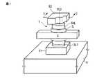
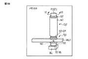
図1は、トランジスタの実施例を示している。図2は、図1のII−II線に沿う断面図である。(Transistor)
FIG. 1 shows an embodiment of a transistor. FIG. 2 is a cross-sectional view taken along the line II-II of FIG.
トランジスタTは、半導体基板11の表面よりも上に配置される。トランジスタTは、第1の電極E1と、第1の電極E1よりも上の第2の電極E2と、第1及び第2の電極E1,E2間のゲート電極Gと、第1及び第2の電極E1,E2間に接続され、ゲート電極Gを貫通する酸化物半導体層SoLと、ゲート電極G及び酸化物半導体層SoL間のゲート絶縁層ILと、を備える。 The transistor T is disposed above the surface of the
第1及び第2の電極E1,E2及びゲート電極Gは、例えば、銅(Cu)及びタングステン(W)のうちの1つを含む。酸化物半導体層SoLは、例えば、酸化インジウム、酸化ガリウム、及び、酸化亜鉛を含む、いわゆるIGZO(InGaZnO)を含む。 The first and second electrodes E1 and E2 and the gate electrode G include, for example, one of copper (Cu) and tungsten (W). The oxide semiconductor layer SoL includes, for example, so-called IGZO (InGaZnO) including indium oxide, gallium oxide, and zinc oxide.
酸化物半導体層SoLは、トランジスタTのチャネルとして機能する。従って、優れたオフリーク特性を持つトランジスタTを実現可能である。チャネルを流れる電流は、半導体基板11の表面に交差する方向となるため、トランジスタTは、縦型トランジスタである。また、ゲート電極Gが酸化物半導体層SoLの側面を取り囲んでおり、その部分がチャネルとして機能するため、大きな駆動力(チャネル幅)を実現可能である。 The oxide semiconductor layer SoL functions as a channel of the transistor T. Therefore, the transistor T having excellent off-leakage characteristics can be realized. Since the current flowing through the channel crosses the surface of the
酸化物半導体層SoLは、酸素を含む。従って、酸化物半導体層SoL内の酸素は、酸化物半導体層SoLと第1の電極E1との界面、及び、酸化物半導体層SoLと第2の電極E2との界面、にそれぞれ金属酸化物層を形成する場合がある。この金属酸化物層は、第1及び第2の電極E1,E2内に含まれる金属の酸化物であり、高抵抗である。 The oxide semiconductor layer SoL contains oxygen. Therefore, oxygen in the oxide semiconductor layer SoL is a metal oxide layer at the interface between the oxide semiconductor layer SoL and the first electrode E1, and at the interface between the oxide semiconductor layer SoL and the second electrode E2, respectively. May form a This metal oxide layer is an oxide of the metal contained in the first and second electrodes E1 and E2, and has high resistance.
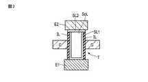
補助層SL1,SL2は、この金属酸化物層の形成を防ぐため、少なくとも、酸化物半導体層SoLと第1の電極E1との間、及び、酸化物半導体層SoLと第2の電極E2との間、に設けられる。即ち、補助層SL1,SL2は、酸化物半導体層SoL内の酸素と第1の電極E1内の金属との反応、及び、酸化物半導体層SoL内の酸素と第2の電極E2内の金属との反応を防止するバリア層として機能する。 In order to prevent the formation of the metal oxide layer, the auxiliary layers SL1 and SL2 at least between the oxide semiconductor layer SoL and the first electrode E1, and between the oxide semiconductor layer SoL and the second electrode E2. Provided between. That is, the auxiliary layers SL1 and SL2 are a reaction of oxygen in the oxide semiconductor layer SoL with a metal in the first electrode E1, and oxygen in the oxide semiconductor layer SoL and a metal in the second electrode E2. Function as a barrier layer to prevent the reaction of
補助層SL1,SL2は、バリア層としての機能を有していれば、どのような材料を用いても構わない。但し、トランジスタTのチャネルが酸化物半導体層SoLであることから、一般的に使用されるバリアメタルを使用するのは望ましくない。なぜなら、酸化物半導体層SoL内の酸素とバリアメタル内の金属が反応して、高抵抗な金属酸化物層を形成してしまうからである。 The auxiliary layers SL1 and SL2 may be made of any material as long as they have a function as a barrier layer. However, since the channel of the transistor T is the oxide semiconductor layer SoL, it is not desirable to use a commonly used barrier metal. This is because the oxygen in the oxide semiconductor layer SoL and the metal in the barrier metal react with each other to form a high-resistance metal oxide layer.
そこで、本実施例では、補助層SL1,SL2も、酸化物層であるのが望ましい。但し、補助層SL1,SL2は、補助層SL1,SL2内の酸素が第1及び第2の電極E1,E2内の金属と反応することを防止するため、酸素の解離エネルギー(dissociation energy)が大きい材料を選択する。ここで、酸素の解離エネルギーとは、補助層SL1,SL2としての酸化物層から酸素を抜き取るために必要なエネルギーのことである。 Therefore, in the present embodiment, it is desirable that the auxiliary layers SL1 and SL2 also be oxide layers. However, since the auxiliary layers SL1 and SL2 prevent the oxygen in the auxiliary layers SL1 and SL2 from reacting with the metal in the first and second electrodes E1 and E2, the dissociation energy (oxygen) of oxygen is large. Select the material. Here, the dissociative energy of oxygen is the energy required to extract oxygen from the oxide layer as the auxiliary layers SL1 and SL2.
例えば、補助層SL1,SL2における酸素の解離エネルギーは、少なくとも、酸化物半導体層SoLにおける酸素の解離エネルギーよりも大きいことが必要である。これにより、補助層SL1と第1の電極E1との間、及び、補助層SL2と第2の電極E2との間、にそれぞれ高抵抗の金属酸化物層が形成されることを防止できるからである。 For example, the dissociation energy of oxygen in the auxiliary layers SL1 and SL2 needs to be at least larger than the dissociation energy of oxygen in the oxide semiconductor layer SoL. This can prevent formation of a metal oxide layer of high resistance between the auxiliary layer SL1 and the first electrode E1 and between the auxiliary layer SL2 and the second electrode E2, respectively. is there.
酸化物層における酸素の解離エネルギーは、酸化物層における酸化物の標準生成エネルギー(standard energy of formation)で言い換えることも可能である。即ち、補助層SL1,SL2における酸素の解離エネルギーが酸化物半導体層SoLにおける酸素の解離エネルギーよりも大きいとは、補助層SL1,SL2における酸化物の標準生成エネルギーが酸化物半導体層SoLにおける酸化物の標準生成エネルギーよりも小さい、ということと等価である。 The dissociation energy of oxygen in the oxide layer can be rephrased in terms of the standard energy of formation of the oxide in the oxide layer. That is, that the dissociation energy of oxygen in the auxiliary layers SL1 and SL2 is larger than the dissociation energy of oxygen in the oxide semiconductor layer SoL means that the standard formation energy of the oxide in the auxiliary layers SL1 and SL2 is an oxide in the oxide semiconductor layer SoL It is equivalent to being smaller than the standard energy of formation of
例えば、補助層SL1,SL2における酸化物の標準生成エネルギーが酸化物半導体層SoLにおける酸化物の標準生成エネルギーよりも小さい場合、補助層SL1,SL2は、酸化物半導体層SoLに比べて、酸化物になり易いため、補助層SL1,SL2内の酸素が第1及び第2の電極E1,E2を酸化するという事態を防ぐことができる。 For example, when the standard formation energy of the oxide in the auxiliary layers SL1 and SL2 is smaller than the standard formation energy of the oxide in the oxide semiconductor layer SoL, the auxiliary layers SL1 and SL2 are oxides compared to the oxide semiconductor layer SoL. Since it is easy to become, it can prevent that the oxygen in auxiliary layer SL1, SL2 oxidizes the 1st and 2nd electrodes E1 and E2.
酸化物半導体層SoLがIGZO(In-Ga-Zn oxide)である場合、補助層SL1,SL2は、以下の材料を選択可能である。 When the oxide semiconductor layer SoL is IGZO (In-Ga-Zn oxide), the following materials can be selected for the auxiliary layers SL1 and SL2.
補助層SL1,SL2も酸化物半導体層とするときは、補助層SL1,SL2は、例えば、Indium-Gallium-Zinc oxide (ex. InGaSiO)、Gallium oxide (ex. Ga2O3)など、のIGZOよりも酸素の解離エネルギーが大きい材料から選択できる。また、補助層SL1,SL2を金属酸化物層とするときは、補助層SL1,SL2は、例えば、Aluminum oxide (ex. Al2O3)、Hafnium oxide (ex. HfO2)など、のIGZOよりも酸素の解離エネルギーが大きく、かつ、第1及び第2の電極E1,E2の酸化物よりも低い抵抗を有する材料から選択できる。When the auxiliary layers SL1 and SL2 are also oxide semiconductor layers, the auxiliary layers SL1 and SL2 may be formed of, for example, IGZO such as Indium-Gallium-Zinc oxide (ex. InGaSiO), Gallium oxide (ex. Ga2 O3 ), etc. It is possible to select from materials having a larger dissociation energy of oxygen. When the auxiliary layers SL1 and SL2 are metal oxide layers, for example, the auxiliary layers SL1 and SL2 are made of IGZO such as Aluminum oxide (ex. Al2 O3 ), Hafnium oxide (ex. HfO2 ), etc. Also, the dissociation energy of oxygen can be selected from materials having high resistance and lower resistance than the oxides of the first and second electrodes E1 and E2.
このように、補助層SL1は、酸化物半導体層SoLと第1の電極E1との間に設けられ、かつ、補助層SL2は、酸化物半導体層SoLと第2の電極E2との間に設けられる。従って、トランジスタTのコンタクト抵抗を低減し、大きな電流駆動力を持つトランジスタTを実現できる。 Thus, the auxiliary layer SL1 is provided between the oxide semiconductor layer SoL and the first electrode E1, and the auxiliary layer SL2 is provided between the oxide semiconductor layer SoL and the second electrode E2. Be Therefore, the contact resistance of the transistor T can be reduced, and the transistor T having a large current driving capability can be realized.
補助層SL1は、例えば、さらに、ゲート絶縁層ILと酸化物半導体層SoLとの間に設けられていてもよい。この場合、補助層SL1は、大きなバンドギャップを有する酸化物層であるのが望ましい。 The auxiliary layer SL1 may be further provided, for example, between the gate insulating layer IL and the oxide semiconductor layer SoL. In this case, the auxiliary layer SL1 is preferably an oxide layer having a large band gap.
例えば、補助層SL1としての酸化物層のバンドギャップエネルギーは、少なくとも、酸化物半導体層SoLのバンドギャップエネルギーよりも大きいことが必要である。これにより、トランジスタTは、いわゆるダブルへテロチャネルを有するHEMT(High Electron Mobility Transistor)と同様の原理により、高いチャネル移動度を有することができるからである。 For example, the band gap energy of the oxide layer as the auxiliary layer SL1 needs to be at least larger than the band gap energy of the oxide semiconductor layer SoL. Thereby, the transistor T can have high channel mobility by the same principle as a so-called HEMT (High Electron Mobility Transistor) having a double hetero channel.
即ち、バンドギャップエネルギーを上述の関係にすれば、トランジスタTにおいて、キャリアが発生する酸化物半導体層SoLをゲート絶縁層ILから離すことにより界面散乱が低減され、結果として、高いチャネル移動度を実現できる。 That is, when the band gap energy is in the above relationship, interface scattering is reduced in the transistor T by separating the oxide semiconductor layer SoL from which carriers are generated from the gate insulating layer IL, and as a result, high channel mobility is realized. it can.
補助層SL1の材料例としてのInGaSiO、Ga2O3、Al2O3、及び、HfO2は、いずれも、酸化物半導体層SoLの材料例としてのIGZOのバンドギャップエネルギーよりも大きなバンドギャップエネルギーを有する。従って、酸化物半導体層SoLがIGZOの場合、補助層SL1として、InGaSiO、Ga2O3、Al2O3、HfO2など、を用いれば、トランジスタTは、高いチャネル移動度により、大きな電流駆動力を有することができる。Each of InGaSiO, Ga2 O3 , Al2 O3 , and HfO2 as a material example of the
尚、ゲート絶縁層ILと酸化物半導体層SoLとの間に存在する補助層SL1は、省略可能である。また、酸化物半導体層SoLは、補助層SL1,SL2により完全に取り囲まれるが、補助層SL1,SL2により取り囲まれない部分を有していてもよい。 The auxiliary layer SL1 present between the gate insulating layer IL and the oxide semiconductor layer SoL can be omitted. In addition, the oxide semiconductor layer SoL may be partially surrounded by the auxiliary layers SL1 and SL2, but may not be surrounded by the auxiliary layers SL1 and SL2.
以上のように、補助層SL1,SL2は、トランジスタTにおいて、低いコンタクト抵抗及び高いチャネル移動度を実現する要素である。 As described above, the auxiliary layers SL1 and SL2 are elements that realize low contact resistance and high channel mobility in the transistor T.
(DRAM)
上述のトランジスタを用いたDRAMの実施例を説明する。(DRAM)
An embodiment of a DRAM using the above-described transistor will be described.
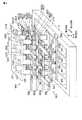
図3は、DRAMの実施例を示している。図4は、図3のデバイス構造の等価回路を示している。 FIG. 3 shows an embodiment of a DRAM. FIG. 4 shows an equivalent circuit of the device structure of FIG.
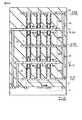
本実施例は、半導体基板11上に、2つのメモリセルアレイMA↓,MA↑を積み重ねたときの構造の例である。但し、半導体基板11上に積み重ねるメモリセルアレイの数は、2n個(n=0,1,2,3,…)であればよい。即ち、2つのメモリセルアレイMA↓,MA↑のうちの1つを省略してもよい。また、2つのメモリセルアレイMA↓,MA↑を1つのペアとして、複数のペアを半導体基板11上に積み重ねてもよい。The present embodiment is an example of a structure in which two memory cell arrays MA ↓ and MA ↑ are stacked on a
半導体基板11は、例えば、単結晶シリコン基板である。半導体基板11上には、メモリセルアレイの周辺回路が配置される。周辺回路とは、リード/ライト時において、メモリセルアレイを駆動するためのCMOS回路のことである。周辺回路は、アドレスデコード回路、リード回路(センスアンプを含む)、ライト回路など、を含む。例えば、センスアンプSA0,SA1,SA2,SA3は、半導体基板11上に配置される。 The
周辺回路としてのセンスアンプSA0,SA1,SA2,SA3は、半導体基板11をチャネル(電流経路)とするトランジスタ(PチャネルFET及びNチャネルFET)を含む。このトランジスタは、例えば、チャネルが半導体基板11の表面に平行な横型トランジスタである。但し、センスアンプSA0,SA1,SA2,SA3内のトランジスタの構造は、特に限定されない。 Sense amplifiers SA0, SA1, SA2 and SA3 as peripheral circuits include transistors (P-channel FET and N-channel FET) having
2つのメモリセルアレイMA↓,MA↑は、半導体基板11の表面よりも上、即ち、センスアンプSA0,SA1,SA2,SA3などの周辺回路よりも上に配置される。 The two memory cell arrays MA ↓ and MA ↑ are disposed above the surface of the
メモリセルアレイMA↓は、複数のワード線WL0↓,WL1↓、複数のビット線BL0,BL1,BL2,BL3,bBL0,bBL1,bBL2,bBL3、及び、複数のメモリセルMC00↓,MC01↓,MC02↓,MC03↓,MC10↓,MC11↓,MC12↓,MC13↓を含む。但し、ワード線の数、ビット線の数、及び、メモリセルの数は、一例であり、これに限定されるという主旨ではない。 The memory cell array MA ↓ includes a plurality of word lines WL0 ↓, WL1 ↓, a plurality of bit lines BL0, BL1, BL2, BL3, bBL0, bBL1, bBL2, bBL3 and a plurality of memory cells MC00 ↓, MC01 ↓, MC02 ↓ , MC0303, MC10 ↓, MC11 ↓, MC12 ↓, MC13 ↓. However, the number of word lines, the number of bit lines, and the number of memory cells are only an example, and the present invention is not intended to be limited thereto.
複数のビット線BL0,BL1,BL2,BL3,bBL0,bBL1,bBL2,bBL3は、半導体基板11の表面に平行な第1の方向に延びる。複数のワード線WL0↓,WL1↓は、半導体基板11の表面に平行で、かつ、第1の方向に交差する第2の方向に延びる。複数のビット線BL0,BL1,BL2,BL3,bBL0,bBL1,bBL2,bBL3、及び、複数のワード線WL0↓,WL1↓は、例えば、銅(Cu)、タングステン(W)など、のメタル材料を備える。 The plurality of bit lines BL 0,
本実施例は、1ビット(相補データ)が2つのメモリセルMC0j↓,MC1j↓により記憶される2セル/1ビット型の例を示す。従って、2本のビット線BLj,bBLjが1つのペアとなって、1つのセンスアンプSAjに接続される。センスアンプSAjは、2つのメモリセルMC0j↓,MC1j↓からの相補データに基づいて、リードデータをセンスする。但し、jは、0、1、2、及び、3のうちの1つである。 This embodiment shows an example of a 2-cell / 1-bit type in which one bit (complementary data) is stored by two memory cells MC0j ↓ and MC1j ↓. Therefore, two bit lines BLj and bBLj form one pair and are connected to one sense amplifier SAj. The sense amplifier SAj senses read data based on complementary data from the two memory cells MC0j ↓ and MC1j ↓. However, j is one of 0, 1, 2, and 3.
本実施例は、2セル/1ビット型の例に限定されるものではない。例えば、本実施例は、1ビットが1つのメモリセルMC0j↓により記憶される1セル/1ビット型に適用することも可能である。この場合、例えば、ワード線WL1↓、複数のビット線bBL0,bBL1,bBL2,bBL3、及び、複数のメモリセルMC10↓,MC11↓,MC12↓,MC13↓は、省略可能である。また、センスアンプSAjは、メモリセルMC0j↓に基づくリード電位とリファレンス電位とを比較することにより、リードデータをセンスする。 The present embodiment is not limited to the example of the 2-cell / 1-bit type. For example, the present embodiment is also applicable to a 1 cell / 1 bit type in which 1 bit is stored by one memory cell MC0j0. In this case, for example, the word line WL1 ↓, the plurality of bit lines bBL0, bBL1, bBL2, bBL3 and the plurality of memory cells MC10 ↓, MC11 ↓, MC12 ↓, MC13 ↓ can be omitted. The sense amplifier SAj senses read data by comparing the read potential based on the memory cell MC0jMC with the reference potential.
メモリセルMC0j↓(jは、0、1、2、及び、3のうちの1つ)は、複数のビット線BL0,BL1,BL2,BL3と、プレート電極12↓と、の間に接続される。プレート電極12↓は、固定電位(例えば、接地電位)に設定される。本実施例は、複数のビット線BL0,BL1,BL2,BL3が、プレート電極12↓よりも上に配置される例を示す。但し、これに代えて、プレート電極12↓が、複数のビット線BL0,BL1,BL2,BL3よりも上に配置されていてもよい。 Memory cell MC 0 j ((j is one of 0, 1, 2, and 3) is connected between a plurality of bit lines BL 0,
複数のビット線BL0,BL1,BL2,BL3がプレート電極12↓よりも上に配置される場合、後述するように、2つのメモリセルアレイMA↓,MA↑で、複数のビット線BL0,BL1,BL2,BL3を共有可能である。これに対し、プレート電極12↓が複数のビット線BL0,BL1,BL2,BL3よりも上に配置される場合、2つのプレート電極12↓,12↑を1つにまとめることができる。 When a plurality of bit lines BL0, BL1, BL2, BL3 are arranged above plate electrode 1212, a plurality of bit lines BL0, BL1, BL2 are formed in two memory cell arrays MA ↓, MA ↑ as described later. , BL3 can be shared. On the other hand, when the
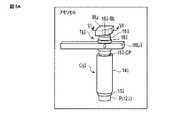
メモリセルMCij↓(iは、0又は1、jは、0、1、2、及び、3のうちの1つ)は、キャパシタCij↓及び選択トランジスタTij↓を備える。 The memory cell MCij ↓ (i is 0 or 1, j is one of 0, 1, 2, and 3) includes a capacitor Cij ↓ and a selection transistor Tij ↓.
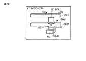
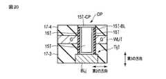
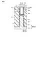
例えば、図5A及び図6Aに示すように、キャパシタCij↓は、プレート電極12↓としてのピラー部Pと、ピラー部Pを覆う絶縁部13↓と、絶縁部13↓を覆うセル電極部14↓と、を備える。選択トランジスタTij↓は、チャネル(電流経路)としての酸化物半導体層(半導体ピラー)15↓と、補助層(supplemental layer)15↓−CP,15↓−BLと、ゲート絶縁層16↓と、ワード線WLi↓と、を備える。 For example, as shown in FIGS. 5A and 6A, the capacitor Cij ↓ has the pillar portion P as the
キャパシタCij↓は、いわゆるフィン型キャパシタである。キャパシタCij↓は、円柱形状を有するが、これに限定されることはない。プレート電極12↓及びセル電極部14↓は、例えば、銅、タングステンなど、のメタル材料を備える。絶縁部13↓は、例えば、銅酸化物、タングステン酸化物、シリコン酸化物、アルミニウム酸化物、ハフニウム酸化物、ジルコニウム酸化物、タンタル酸化物や、これらの積層構造など、を含む。 The capacitor Cij ↓ is a so-called fin-type capacitor. The capacitor Cij ↓ has a cylindrical shape, but is not limited thereto. The
選択トランジスタTij↓は、例えば、半導体基板11よりも上に配置されるチャネルとしての酸化物半導体層15↓を備え、かつ、チャネルが半導体基板11の表面に交差する縦型トランジスタである。また、酸化物半導体層15↓は、ワード線WLi↓を貫通する。即ち、ワード線WLi↓は、酸化物半導体層15↓の側面(周囲)を取り囲む。 The selection transistor Tij ↓ is, for example, a vertical transistor including an
この場合、選択トランジスタTij↓のチャネル幅が酸化物半導体層15↓の周方向となるため、選択トランジスタTij↓の駆動力を大きくできる。また、ワード線WLiのピッチを2Fとし、ビット線BLjのピッチを2Fとしたとき、メモリセルMCij↓の平面サイズは、4F2を実現できる。In this case, since the channel width of the selection transistor Tij と な る is in the circumferential direction of the
また、図3に示すように、本例では、2つのメモリセルMCij↓,MCij↑が4F2のエリア内に配置される。この場合、2セル/4F2を実現できる。これは、半導体基板11上に積み重ねるメモリセルアレイMA↓,MA↑の数を増やせば、さらに、1セル当たりの平面サイズを小さくできることを意味する。即ち、半導体基板11上にn個のメモリセルを積み重ねる場合、nセル/4F2を実現できる。Further, as shown in FIG. 3, in this example, two memory cells MCij ↓, MCij ↑ is disposed within the 4F2 area. In this case, it is possible to realize a two-cell / 4F2. This means that the planar size per cell can be further reduced by increasing the number of memory cell arrays MA 増 and MA 平面 stacked on the
但し、Fは、フューチャーサイズ(配線の最小加工幅)であり、平面サイズは、半導体基板11の表面に平行な面内でのサイズのことを意味する。また、nセルは、n個のメモリセルを意味し、nは、1以上の自然数(1,2,3,…)である。 However, F is the feature size (minimum processing width of wiring), and the plane size means the size in a plane parallel to the surface of the
酸化物半導体層15↓は、例えば、IGZO(InGaZnO)を含む。酸化物半導体層15↓をチャネルとするトランジスタは、例えば、200℃程度の低温プロセスで形成することが可能であるため、ウェハプロセスにおいて半導体基板11の表面領域内の周辺回路に熱ストレスを与えないという意味で、DRAMの三次元化に非常に有効である。また、酸化物半導体層15↓をチャネルとするトランジスタは、一般的なシリコンチャネルトランジスタに比べて、オフ時のリーク電流を大幅に削減できる。このため、非常に長いデータ保持時間(リテンションタイム)を持つDRAMを実現できる。 The
例えば、シリコンをチャネルとする選択トランジスタTij↓の場合、リテンションタイムは、64msec程度である。このため、短い周期でデータのリフレッシュ(再書き込み)を行わなければならない。これに対し、IGZOをチャネルとする選択トランジスタTij↓の場合、リテンションタイムは、10days程度である。このため、データのリフレッシュがシステムのパフォーマンスに影響を与えることがない。 For example, in the case of the selection transistor Tij ↓ having silicon as a channel, the retention time is about 64 msec. Therefore, data must be refreshed (rewritten) in a short cycle. On the other hand, in the case of the selection transistor Tij ↓ having IGZO as a channel, the retention time is about 10 days. Therefore, data refresh does not affect system performance.
補助層15↓−CP,15↓−BLは、少なくとも、酸化物半導体層15↓とセル電極部14↓との間、及び、酸化物半導体層15↓とビット線BLjとの間、に設けられる。即ち、補助層15↓−CP,15↓−BLは、酸化物半導体層15↓内の酸素とセル電極部14↓内の金属との反応、及び、酸化物半導体層15↓内の酸素とビット線BLj内の金属との反応を防止するバリア層として機能する。 The
補助層15↓−CP,15↓−BLは、図1及び図2のトランジスタTの補助層SL1,SL2と同様に、酸化物層であるのが望ましい。但し、補助層15↓−CP,15↓−BLは、補助層15↓−CP,15↓−BL内の酸素がセル電極部14↓内の金属又はビット線BLj内の金属と反応することを防止するため、酸素の解離エネルギーが大きい材料を選択する。 Similar to the auxiliary layers SL1 and SL2 of the transistor T in FIGS. 1 and 2, the
例えば、補助層15↓−CP,15↓−BLにおける酸素の解離エネルギーは、少なくとも、酸化物半導体層15↓における酸素の解離エネルギーよりも大きいことが必要である。これにより、補助層15↓−CPとセル電極部14↓との間、及び、補助層15↓−BLとビット線BLjとの間、にそれぞれ高抵抗の金属酸化物層(例えば、銅、タングステンなどの酸化物)が形成されることを防止できるからである。 For example, the dissociation energy of oxygen in the
酸化物半導体層15↓及び補助層15↓−CP,15↓−BLの材料例は、図1及び図2のトランジスタTの酸化物半導体層SoL及び補助層SL1,SL2の材料例と同じであるため、ここでの説明を省略する。 The material examples of the
このように、補助層15↓−CPは、酸化物半導体層15↓とセル電極部14↓との間に設けられ、かつ、補助層15↓−BLは、酸化物半導体層15↓とビット線BLjとの間に設けられる。従って、選択トランジスタTij↓のコンタクト抵抗を低減し、大きな電流駆動力を持つ選択トランジスタTij↓を実現できる。 As described above, the
本実施例では、後述するように、製造プロセス上、補助層15↓−CPは、酸化物半導体層15↓とゲート絶縁層16↓との間にも設けられる。これについては、製造プロセスの説明において詳しく述べる。この場合、図1及び図2のトランジスタTの実施例で説明した理由と同様の理由により、補助層15↓−CPとしての酸化物層のバンドギャップエネルギーは、少なくとも、酸化物半導体層15↓のバンドギャップエネルギーよりも大きいのが望ましい。 In the present embodiment, as described later, the
尚、選択トランジスタTij↓のチャネルとしての半導体層15↓は、円柱形状を有するが、これに限定されることはない。 The
本実施例では、メモリセルアレイMA↓において、1本のビット線BLj(jは、0、1、2、及び、3のうちの1つ)に、1つのメモリセルMCij↓(i=0)が接続され、1本のビット線bBLj(jは、0、1、2、及び、3のうちの1つ)に、1つのメモリセルMCij↓(i=1)が接続される。これは、図面が複雑化するのを防ぐためであり、ビット線BLj及びビット線bBLjには、それぞれ、複数のメモリセルが接続されていてもよい。 In this embodiment, in the memory cell array MA (, one memory cell MCij ↓ (i = 0) is connected to one bit line BLj (j is one of 0, 1, 2, and 3). One memory cell MCij ↓ (i = 1) is connected to one bit line bBLj (j is one of 0, 1, 2, and 3). This is to prevent the drawing from being complicated, and a plurality of memory cells may be connected to the bit line BLj and the bit line bBLj, respectively.
メモリセルアレイMA↓の第1の方向の端部には、イコライズトランジスタ(FET)EQij↓(iは、0又は1、jは、0、1、2、及び、3のうちの1つ)が配置される。イコライズトランジスタEQij↓(i=0)は、例えば、リードの準備段階として、ビット線BLjの電位を所定電位(例えば、Vdd/2、Vddは電源電位)Vpreにプリチャージする。同様に、イコライズトランジスタEQij↓(i=1)は、例えば、リード時の準備段階として、ビット線bBLjの電位を所定電位Vpreにプリチャージする。 At the end of the first direction of the memory cell array MA ↓, equalizing transistors (FETs) EQij ↓ (where i is 0 or 1, j is one of 0, 1, 2 and 3) are arranged Be done. The equalizing transistor EQij ↓ (i = 0) precharges the potential of the bit line BLj to a predetermined potential (for example, Vdd / 2, Vdd is a power supply potential) Vpre, for example, as a read preparation step. Similarly, the equalizing transistor EQij ↓ (i = 1) precharges the potential of the bit line bBLj to the predetermined potential Vpre, for example, as a preparation step at the time of reading.
イコライズトランジスタEQij↓は、例えば、リードの準備段階として、2本のビット線BLj,bBLjを所定電位にイコライズすることから、イコライズトランジスタと呼ばれる。ここで、イコライズトランジスタEQij↓は、メモリセルMCij↓と同様に、半導体基板11の表面よりも上に配置される。 The equalizing transistor EQij ↓ is called an equalizing transistor because it equalizes the two bit lines BLj and bBLj to a predetermined potential, for example, as a read preparation step. Here, the equalizing transistor EQij ↓ is disposed above the surface of the
例えば、イコライズトランジスタEQij↓は、メモリセルMCij↓と同じ層(半導体基板11の表面からの距離が同じ領域)内に配置される。これにより、イコライズトランジスタEQij↓とビット線BLj,bBLjとの距離を短くし、ビット線BLj,bBLjの充放電(イコライズ)を高速に行うことができる。 For example, the equalizing transistor EQij ↓ is disposed in the same layer as the memory cell MCij ↓ (in the same area as the distance from the surface of the semiconductor substrate 11). Thus, the distance between the equalizing transistor EQij ↓ and the bit lines BLj and bBLj can be shortened, and charging / discharging (equalizing) of the bit lines BLj and bBLj can be performed at high speed.
イコライズトランジスタEQij↓(i=0)は、所定電位Vpreを有するイコライズ電位線EQL↓と、複数のビット線BL0,BL1,BL2,BL3と、の間に接続される。同様に、イコライズトランジスタEQij↓(i=1)は、所定電位Vpreを有するイコライズ電位線EQL↓と、複数のビット線bBL0,bBL1,bBL2,bBL3と、の間に接続される。イコライズ電位線EQL↓は、第2の方向に延びる。 The equalizing transistor EQij ↓ (i = 0) is connected between an equalizing potential line EQL ↓ having a predetermined potential Vpre and a plurality of bit lines BL0, BL1, BL2, and BL3. Similarly, the equalizing transistor EQij ↓ (i = 1) is connected between the equalizing potential line EQL ↓ having the predetermined potential Vpre and the plurality of bit lines bBL0, bBL1, bBL2, bBL3. Equalize potential line EQL ↓ extends in the second direction.
イコライズトランジスタEQij↓は、例えば、図7A及び図8Aに示すように、チャネル(電流経路)としての酸化物半導体層(半導体ピラー)15’↓と、ゲート絶縁層16’↓と、ゲートイコライズ線GEQ↓と、補助層15’↓−EQL,15’↓−BLと、を備える。ゲートイコライズ線GEQ↓は、第2の方向に延びる。 For example, as shown in FIG. 7A and FIG. 8A, the equalizing transistor EQij.perp., An oxide semiconductor layer (semiconductor pillar) 15'.perp. As a channel (current path), a
イコライズトランジスタEQij↓は、例えば、選択トランジスタTij↓と同様に、チャネルが半導体基板11の表面に交差する縦型トランジスタである。従って、イコライズトランジスタEQij↓のチャネル幅が酸化物半導体層15’↓の周方向となるため、イコライズトランジスタEQij↓の駆動力を大きくできる。 The equalizing transistor EQij ↓ is, for example, a vertical transistor in which the channel intersects the surface of the
また、イコライズトランジスタEQij↓は、例えば、選択トランジスタTij↓と同様に、酸化物半導体層15’↓をチャネルとする。従って、イコライズトランジスタEQij↓は、優れたオフリーク特性を有する。さらに、イコライズトランジスタEQij↓は、例えば、選択トランジスタTij↓と同様に、補助層15’↓−EQL,15’↓−BLを備える。従って、イコライズトランジスタEQij↓は、低いコンタクト抵抗と高いチャネル移動度を有する。 Further, the equalizing transistor EQij ↓ uses, for example, the oxide semiconductor layer 15 'チ ャ ネ ル as a channel, similarly to the selection transistor Tij ↓. Therefore, the equalizing transistor EQij ↓ has excellent off-leak characteristics. Furthermore, the equalizing transistor EQij ↓ includes, for example, the auxiliary layers 15'EQ-EQL and 15 '↓ -BL, similarly to the selection transistor Tij ↓. Accordingly, the equalizing transistor EQij ↓ has low contact resistance and high channel mobility.
イコライズトランジスタEQij↓の構造は、選択トランジスタTij↓の構造と同じであるため、ここでの詳細な説明を省略する。但し、酸化物半導体層15’↓、ゲート絶縁層16’↓、ゲートイコライズ線GEQ↓、及び、補助層15’↓−EQL,15’↓−BLは、それぞれ、酸化物半導体層15↓、ゲート絶縁層16↓、ワード線WLi↓、及び、補助層15↓−CP,15↓−BLに対応する。 Since the structure of the equalizing transistor EQij 同 じ is the same as the structure of the selecting transistor Tij ↓, the detailed description thereof is omitted here. However, the
メモリセルアレイMA↑は、メモリセルアレイMA↓上に配置される。即ち、2つのメモリセルアレイMA↓,MA↑は、第1及び第2の方向に交差する第3の方向に積み重ねられる。メモリセルアレイMA↑は、メモリセルアレイMA↓と同様の構造を有する。 Memory cell array MA ↑ is disposed on memory cell array MA ↓. That is, the two memory cell arrays MA ↓ and MA ↑ are stacked in a third direction crossing the first and second directions. Memory cell array MA ↑ has the same structure as memory cell array MA ↓.
但し、メモリセルアレイMA↑は、メモリセルアレイMA↓に対して、上下が反転した構造(複数のビット線BL0,BL1,BL2,BL3,bBL0,bBL1,bBL2,bBL3に対して対称な構造)を有する。また、本実施例では、複数のビット線BL0,BL1,BL2,BL3,bBL0,bBL1,bBL2,bBL3が、2つのメモリセルアレイMA↓,MA↑で共有化される。 However, the memory cell array MA ↑ has a structure (symmetrical to the plurality of bit lines BL0, BL1, BL2, BL3, bBL0, bBL1, bBL2, bBL3) upside down with respect to the memory cell array MA ↓. . Further, in the present embodiment, the plurality of bit lines BL0, BL1, BL2, BL3, bBL0, bBL1, bBL2, bBL3 are shared by two memory cell arrays MA ↓, MA ↑.
メモリセルアレイMA↑は、複数のワード線WL0↑,WL1↑、複数のビット線BL0,BL1,BL2,BL3,bBL0,bBL1,bBL2,bBL3、及び、複数のメモリセルMC00↑,MC01↑,MC02↑,MC03↑,MC10↑,MC11↑,MC12↑,MC13↑を含む。但し、ワード線の数、ビット線の数、及び、メモリセルの数は、一例であり、これに限定されるという主旨ではない。 The memory cell array MA ↑ includes a plurality of word lines WL0 ↑, WL1 ↑, a plurality of bit lines BL0, BL1, BL2, BL3, bBL0, bBL1, bBL2, bBL3 and a plurality of memory cells MC00 ↑, MC01 ↑, MC02 ↑ , MC03 ↑, MC10 ↑, MC11 ↑, MC12 ↑, MC13 ↑. However, the number of word lines, the number of bit lines, and the number of memory cells are only an example, and the present invention is not intended to be limited thereto.
複数のワード線WL0↑,WL1↑は、第2の方向に延びる。メモリセルアレイMA↑は、メモリセルアレイMA↓と同様に、2セル/1ビット型の例を示すが、1セル/1ビット型に変えることもできる。この場合、例えば、ワード線WL1↑、複数のビット線bBL0,bBL1,bBL2,bBL3、及び、複数のメモリセルMC10↑,MC11↑,MC12↑,MC13↑は、省略可能である。 The plurality of word lines WL0 ↑ and WL1 ↑ extend in the second direction. Similar to the memory cell array MA ↓, the memory cell array MA ↑ shows an example of a 2 cell / 1 bit type, but can be changed to a 1 cell / 1 bit type. In this case, for example, the word line WL1 ↑, the plurality of bit lines bBL0, bBL1, bBL2, bBL3 and the plurality of memory cells MC10 ↑, MC11 ↑, MC12 ↑, MC13 ↑ can be omitted.
メモリセルMC0j↑(jは、0、1、2、及び、3のうちの1つ)は、複数のビット線BL0,BL1,BL2,BL3と、プレート電極12↑と、の間に接続される。プレート電極12↑は、固定電位(例えば、接地電位)に設定される。プレート電極12↑は、複数のビット線BL0,BL1,BL2,BL3よりも上に配置されるが、複数のビット線BL0,BL1,BL2,BL3がプレート電極12↑よりも上に配置されていてもよい。 Memory cell MC0j ↑ (j is one of 0, 1, 2, and 3) is connected between a plurality of bit lines BL0, BL1, BL2, BL3 and
メモリセルMCij↑(iは、0又は1、jは、0、1、2、及び、3のうちの1つ)は、キャパシタCij↑及び選択トランジスタTij↑を備える。例えば、図5B及び図6Bに示すように、キャパシタCij↑は、プレート電極12↑としてのピラー部Pと、ピラー部Pを覆う絶縁部13↑と、絶縁部13↑を覆うセル電極部14↑と、を備える。選択トランジスタTij↑は、チャネルとしての酸化物半導体層(半導体ピラー)15↑と、補助層15↑−BL,15↑−CPと、ゲート絶縁層16↑と、ワード線WLi↑と、を備える。 The memory cell MCij ↑ (i is 0 or 1, j is 0, 1, 2, and one of 3) includes a capacitor Cij ↑ and a selection transistor Tij ↑. For example, as shown in FIGS. 5B and 6B, the capacitor Cij ↑ has the pillar portion P as the
キャパシタCij↑は、いわゆるフィン型キャパシタである。キャパシタCij↑は、円柱形状を有するが、これに限定されることはない。プレート電極12↑及びセル電極部14↑は、例えば、銅、タングステンなど、のメタル材料を備える。絶縁部13↑は、例えば、銅酸化物、タングステン酸化物、シリコン酸化物、アルミニウム酸化物、ハフニウム酸化物、ジルコニウム酸化物、タンタル酸化物や、これらの積層構造など、を含む。 The capacitor Cij ↑ is a so-called fin-type capacitor. The capacitor Cij ↑ has a cylindrical shape, but is not limited thereto. The
選択トランジスタTij↑は、例えば、半導体基板11よりも上に配置されるチャネルとしての酸化物半導体層15↑を備え、かつ、チャネルが半導体基板11の表面に交差する縦型トランジスタである。また、選択トランジスタTij↑は、補助層15↓−CP,15↓−BLにより、低いコンタクト抵抗及び高いチャネル移動度を有する。 The selection transistor Tij ↑ is, for example, a vertical transistor including an
選択トランジスタTij↑のチャネルとしての酸化物半導体層15↑は、円柱形状を有するが、これに限定されることはない。ゲート絶縁層16↑は、例えば、酸化シリコンなどの絶縁体を備える。ワード線WLi↑は、例えば、銅、タングステンなど、のメタル材料を備える。 The
また、メモリセルアレイMA↑において、複数のメモリセルが1本のビット線BLj(jは、0、1、2、及び、3のうちの1つ)に接続されていてもよいし、複数のメモリセルが1本のビット線bBLj(jは、0、1、2、及び、3のうちの1つ)に接続されていてもよい。 In memory cell array MA セ ル, a plurality of memory cells may be connected to one bit line BLj (j is one of 0, 1, 2, and 3), or a plurality of memories The cell may be connected to one bit line bBLj (j is one of 0, 1, 2, and 3).
メモリセルアレイMA↑の第1の方向の端部には、イコライズトランジスタ(FET)EQij↑(iは、0又は1、jは、0、1、2、及び、3のうちの1つ)が配置される。メモリセルアレイMA↑内のイコライズトランジスタEQij↑の構造及び機能は、メモリセルアレイMA↓内のイコライズトランジスタEQij↓の構造及び機能と同じである。 At the end of the first direction of the memory cell array MA ↑, equalizing transistors (FETs) EQij ↑ (i is 0 or 1, j is one of 0, 1, 2 and 3) are arranged Be done. The structure and function of the equalizing transistors EQij ↑ in the memory cell array MA ↑ are the same as the structure and functions of the equalizing transistors EQij ↓ in the memory cell array MA イ コ ラ イ.
イコライズトランジスタEQij↑は、例えば、図7B及び図8Bに示すように、チャネルとしての酸化物半導体層(半導体ピラー)15’↑と、補助層15’↑−BL,15’↑−EQLと、ゲート絶縁層16’↑と、ゲートイコライズ線GEQ↑と、を備える。ゲートイコライズ線GEQ↑は、第2の方向に延びる。 For example, as shown in FIGS. 7B and 8B, the equalizing transistor EQij ↑ has a gate as a channel, an oxide semiconductor layer (semiconductor pillar) 15 ′ ↑, an
イコライズトランジスタEQij↑は、例えば、選択トランジスタTij↑と同様に、チャネルが半導体基板11の表面に交差する縦型トランジスタである。従って、イコライズトランジスタEQij↑のチャネル幅が酸化物半導体層15’↑の周方向となるため、イコライズトランジスタEQij↑の駆動力を大きくできる。 The equalizing transistor EQij ↑ is, for example, a vertical transistor in which a channel intersects the surface of the
また、イコライズトランジスタEQij↑は、例えば、選択トランジスタTij↑と同様に、酸化物半導体層15’↑をチャネルとする。従って、イコライズトランジスタEQij↑は、優れたオフリーク特性を有する。さらに、イコライズトランジスタEQij↑は、例えば、選択トランジスタTij↑と同様に、補助層15’↑−BL,15’↑−EQLを備える。従って、イコライズトランジスタEQij↑は、低いコンタクト抵抗と高いチャネル移動度を有する。 Further, the equalizing transistor EQij ↑, for example, uses the oxide semiconductor layer 15 'チ ャ ネ ル as a channel, similarly to the selection transistor Tij ↑. Therefore, the equalizing transistor EQij ↑ has excellent off-leak characteristics. Furthermore, the equalizing transistor EQij ↑, for example, includes an auxiliary layer 15 '↑ -BL, 15' ↑ -EQL, similarly to the selection transistor Tij ↑. Thus, the equalizing transistor EQij ↑ has low contact resistance and high channel mobility.
イコライズトランジスタEQij↑の構造は、選択トランジスタTij↑の構造と同じであるため、ここでの詳細な説明を省略する。但し、酸化物半導体層15’↑、ゲート絶縁層16’↑、ゲートイコライズ線GEQ↑、及び、補助層15’↑−BL,15’↑−EQLは、それぞれ、酸化物半導体層15↑、ゲート絶縁層16↑、ワード線WLi↑、及び、補助層15↑−BL,15↑−CPに対応する。 The structure of the equalizing transistor EQij ↑ is the same as the structure of the selecting transistor Tij ↑, and thus the detailed description thereof is omitted here. However, the
本実施例では、複数のビット線BL0,BL1,BL2,BL3,bBL0,bBL1,bBL2,bBL3の上下に、それぞれ、イコライズトランジスタEQij↓,EQij↑が接続されるが、そのうちの一方を省略してもよい。 In this embodiment, equalizing transistors EQijij and EQij ↑ are respectively connected to the upper and lower sides of the plurality of bit lines BL0, BL1, BL2, BL3, bBL0, bBL1, bBL2, bBL3, but one of them is omitted. It is also good.
例えば、イコライズトランジスタEQij↓を省略し、メモリセルアレイMA↑側のみにイコライズトランジスタEQij↑を設けてもよいし、イコライズトランジスタEQij↑を省略し、メモリセルアレイMA↓側のみにイコライズトランジスタEQij↓を設けてもよい。これは、2つのメモリセルアレイMA↓,MA↑で、複数のビット線BL0,BL1,BL2,BL3,bBL0,bBL1,bBL2,bBL3を共有しているから可能なことである。 For example, equalization transistors EQijij may be omitted, equalization transistors EQij イ コ ラ イ may be provided only on the memory cell array MA ↑ side, equalization transistors EQij イ コ ラ イ may be omitted, and equalization transistors EQij ↓ may be provided only on the memory cell array MA 設 け side. It is also good. This is possible because the plurality of bit lines BL0, BL1, BL2, BL3, bBL0, bBL1, bBL2, bBL3 are shared by the two memory cell arrays MA ↓, MA ↑.
但し、本実施例のように、複数のビット線BL0,BL1,BL2,BL3,bBL0,bBL1,bBL2,bBL3の上下に、それぞれ、イコライズトランジスタEQij↓,EQij↑を接続すれば、イコライズトランジスタEQij↓,EQij↑の駆動力が大きくなることで、複数のビット線BL0,BL1,BL2,BL3,bBL0,bBL1,bBL2,bBL3の充放電(イコライズ)をさらに高速化できる。 However, if equalizing transistors EQij ↓ and EQij ↑ are respectively connected to the upper and lower sides of a plurality of bit lines BL0, BL1, BL2, BL3, bBL0, bBL1, bBL2 and bBL3 as in this embodiment, the equalizing transistors EQij ↓ By increasing the driving power of the plurality of bit lines, the charge / discharge (equalize) of the plurality of bit lines BL0, BL1, BL2, BL3, bBL0, bBL1, bBL2, bBL3 can be further speeded up.
(製造方法)
上述のDRAMの製造方法の例を説明する。(Production method)
An example of the above-described DRAM manufacturing method will be described.
ここでは、本実施例の主要部である選択トランジスタの製造方法の例を説明する。 Here, an example of a method of manufacturing the selection transistor, which is a main part of the present embodiment, will be described.
図5A及び図6Aの選択トランジスタTij↓の製造方法は、図9、図10、図13、図15、図17、図19、及び、図21に示す。また、図5B及び図6Bの選択トランジスタTij↑の製造方法は、図11、図12、図14、図16、図18、図20、及び、図22に示す。さらに、図7A、図8A、図7B、及び、図8BのイコライズトランジスタEQij↓,EQij↑の製造方法は、図9乃至図22の製造方法をそのまま適用可能である。 A method of manufacturing the selection transistor Tij in FIGS. 5A and 6A is shown in FIGS. 9, 10, 13, 15, 17, 19, 21 and 23. The method of manufacturing the select transistor TijT in FIGS. 5B and 6B is shown in FIGS. 11, 12, 14, 16, 18, 20, and 22. Further, the manufacturing methods of FIG. 9 to FIG. 22 can be applied as they are as the manufacturing methods of the equalizing transistors EQij ↓ and EQij ↑ in FIGS. 7A, 8A, 7B and 8B.
まず、図9乃至図12に示すように、キャパシタCij↓又はビット線BLjを形成する。キャパシタCij↓は、プレート電極12↓(ピラー部Pを含む)、絶縁部13↓、及び、セル電極部14↓を含む。これらは、CVD(Chemical Vapor deposition)などの堆積法、PEP(Photo Engraving Process)などの加工法、及び、RIE(Reactive Ion Etching)/CMP(Chemical Mechanical Polishing)などのエッチング/研磨法を組み合わせることにより容易に形成可能である。 First, as shown in FIGS. 9 to 12, capacitors Cij ↓ or bit lines BLj are formed. The capacitor Cij ↓ includes the
同様に、キャパシタCij↓上、又は、ビット線BLj上に、第2の方向に延びるワード線WLi↓又はワード線WLi↑を形成する。ここで、本製造方法における第1、第2、及び、第3の方向は、図3及び図4における第1、第2、及び、第3の方向に対応する。 Similarly, word line WLii or word line WLiWL extending in the second direction is formed on capacitor Cij ↓ or bit line BLj. Here, the first, second and third directions in the present manufacturing method correspond to the first, second and third directions in FIGS. 3 and 4.
また、図9及び図10に示すように、キャパシタCij↓を覆う層間絶縁層17−1を形成し、ワード線WLi↓を覆う層間絶縁層17−2を形成する。また、図11及び図12に示すように、ビット線BLjを覆う層間絶縁層17−3を形成し、ワード線WLi↑を覆う層間絶縁層17−4を形成する。 Further, as shown in FIGS. 9 and 10, an interlayer insulating layer 17-1 covering the capacitor Cijij is formed, and an interlayer insulating layer 17-2 covering the word line WLi 形成 is formed. Further, as shown in FIGS. 11 and 12, the interlayer insulating layer 17-3 covering the bit line BLj is formed, and the interlayer insulating layer 17-4 covering the word line WLi ↑ is formed.
この後、例えば、PEP及びRIEにより、層間絶縁層17−1,17−2,17−3,17−4内に、開口(ビア又はスルーホール)OPを形成する。図9及び図11に示すように、開口OPは、ワード線WLi↓又はワード線WLi↑を貫通するようにアライメントされる。開口OPの底部は、セル電極部14↓又はビット線BLjに達する。 Thereafter, for example, the openings (vias or through holes) OP are formed in the interlayer insulating layers 17-1, 17-2, 17-3, and 17-4 by PEP and RIE. As shown in FIGS. 9 and 11, the opening OP is aligned so as to penetrate the word line WLi ↓ or the word line WLi ↑. The bottom of the opening OP reaches the cell electrode portion 14 ↓ or the bit line BLj.
次に、図13及び図14に示すように、例えば、CVDにより、層間絶縁層17−2,17−4上、及び、開口OPの内面上に、それぞれ、ゲート絶縁層16↓,16↑を形成する。続けて、例えば、RIEにより、ゲート絶縁層16↓,16↑をエッチングし、開口OP内に露出するワード線(ゲート電極G)WLi↓の側面上、又は、開口OP内に露出するワード線(ゲート電極G)WLi↑の側面上に、ゲート絶縁層16↓,16↑を残存させる。 Next, as shown in FIGS. 13 and 14, for example, the
次に、図15及び図16に示すように、例えば、CVDにより、層間絶縁層17−2,17−4上、及び、開口OPの内面上に、それぞれ、補助層15↓−CP,15↑−BLを形成する。続けて、例えば、CVDにより、層間絶縁層17−2,17−4上に、開口OPを完全に満たす酸化物半導体層15↓,15↑を形成する。 Next, as shown in FIGS. 15 and 16, for example, auxiliary layers 15CVD-CP, 15 ↑ are formed on the interlayer insulating layers 17-2 and 17-4 and the inner surface of the opening OP, respectively, by CVD. Form -BL. Subsequently, oxide semiconductor layers 15 ↓ and 15 ↑ completely filling the opening OP are formed on the interlayer insulating layers 17-2 and 17-4 by, for example, CVD.
ここで、補助層15↓−CP,15↑−BLは、上述したように、セル電極部14↓又はビット線BLjの表面上に金属酸化物を形成し難い材料を備えるため、酸化物半導体層15↓,15↑と、セル電極部14↓又はビット線BLjとのコンタクト抵抗を低減することができる。 Here, as described above, the
また、選択トランジスタTij↓,Tij↑のチャネルとしての酸化物半導体層15↓,15↑とゲート絶縁層16↓,16↑との間には、チャネルを移動するキャリアの界面散乱を低減する補助層15↓−CP,15↑−BLが存在するため、上述したように、選択トランジスタTij↓,Tij↑において、キャリアのチャネル移動度を向上させることができる。 In addition, an auxiliary layer that reduces interface scattering of carriers moving in the channel between the oxide semiconductor layers 15 ↓ and 15 ↑ as channels of the selection transistors Tij ↓ and Tij ↑ and the
次に、図17及び図18に示すように、例えば、第1のCMPにより、酸化物半導体層15↓,15↑、及び、補助層15↓−CP,15↑−BLを研磨し、これらを開口OP内に残存させる。第1のCMPは、層間絶縁層17−2,17−4の表面が露出するまで行われる。また、第1のCMPでは、酸化物半導体層15↓,15↑のエッチングレート、及び、補助層15↓−CP,15↑−BLのエッチングレートが層間絶縁層17−2,17−4のエッチングレートよりも大きくなるように、研磨剤(スラリー)の成分が選択される。 Next, as shown in FIGS. 17 and 18, for example, the oxide semiconductor layers 15 ↑ and 15 補助 and the
また、第1のCMPは、層間絶縁層17−2,17−4の上面(第3の方向にある表面)が露出した後もエッチング(研磨)を継続する、いわゆるオーバーエッチングにより実行される。その結果、酸化物半導体層15↓,15↑の上面、及び、補助層15↓−CP,15↑−BLの上面は、層間絶縁層17−2,17−4の上面よりも下(半導体基板11に近い位置)となる。 The first CMP is performed by so-called over-etching in which etching (polishing) is continued even after the upper surfaces (surfaces in the third direction) of the interlayer insulating layers 17-2 and 17-4 are exposed. As a result, the upper surfaces of the oxide semiconductor layers 15 ↓ and 15 ↑ and the upper surfaces of the
次に、図19及び図20に示すように、例えば、CVDにより、層間絶縁層17−2,17−4上、及び、酸化物半導体層15↓,15↑上に、それぞれ、補助層15↓−BL,15↑−CPを形成する。続けて、第2のCMPにより、補助層15↓−BL,15↑−CPを研磨し、これらを開口OP内に残存させる。第2のCMPは、層間絶縁層17−2,17−4の表面が露出するまで行われる。また、第2のCMPでは、補助層15↓−BL,15↑−CPのエッチングレートが層間絶縁層17−2,17−4のエッチングレートよりも大きくなるように、研磨剤(スラリー)の成分が選択される。 Next, as shown in FIGS. 19 and 20, the
第2のCMPは、第1のCMPとは異なり、層間絶縁層17−2,17−4の上面が露出した時点でエッチング(研磨)を停止する。その結果、補助層15↓−BL,15↑−CPの上面は、層間絶縁層17−2,17−4の上面とほぼ同じ位置となる。 The second CMP, unlike the first CMP, stops the etching (polishing) when the upper surfaces of the interlayer insulating layers 17-2 and 17-4 are exposed. As a result, the upper surfaces of the
以上の工程により、酸化物半導体層15↓は、補助層15↓−CP,15↓−BLにより取り囲まれる。また、酸化物半導体層15↑は、補助層15↑−BL,15↑−CPにより取り囲まれる。 By the above steps, the
次に、図21に示すように、補助層15↓−BL上にビット線BLjを形成することにより、例えば、図3のメモリセルアレイMA↓内のメモリセルMCijが形成される。ここで、補助層15↓−BLは、上述したように、ビット線BLjの表面(下面)上に金属酸化物を形成し難い材料を備えるため、酸化物半導体層15↓とビット線BLjとのコンタクト抵抗を低減することができる。 Next, as shown in FIG. 21, by forming the bit line BLj on the
同様に、図22に示すように、補助層15↑−CP上にキャパシタCij↑を形成することにより、例えば、図3のメモリセルアレイMA↑内のメモリセルMCijが形成される。キャパシタCij↑は、プレート電極12↑(ピラー部Pを含む)、絶縁部13↑、及び、セル電極部14↑を含む。これらは、CVDなどの堆積法、PEPなどの加工法、及び、RIE/CMPなどのエッチング/研磨法を組み合わせることにより容易に形成可能である。 Similarly, as shown in FIG. 22, by forming the capacitor Cij ↑ on the
ここで、補助層15↑−CPは、上述したように、セル電極部14↑の表面(下面)上に金属酸化物を形成し難い材料を備えるため、酸化物半導体層15↑とセル電極部14↑とのコンタクト抵抗を低減することができる。 Here, as described above, since the
(応用例)
図3及び図4のDRAMの応用例を説明する。(Application example)
An application example of the DRAM of FIGS. 3 and 4 will be described.
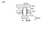
図23は、DRAMの平面図を示している。図24A及び図24Bは、図23のXX−IV−XXIV線に沿う断面図である。 FIG. 23 shows a plan view of the DRAM. 24A and 24B are cross-sectional views taken along the line XX-IV-XXIV of FIG.
図24Aの例では、半導体基板11上に、複数のユニットU0、U1,…が積み重ねられる。複数のユニットU0、U1,…の各々は、図3及び図4に示す2つのメモリセルアレイMA↓,MA↑を備える。即ち、図24AのエリアXに示すように、2つのメモリセルアレイMA↓,MA↑において、ビット線BL_1st, BL_2ndが共有される。 In the example of FIG. 24A, a plurality of units U0, U1,... Are stacked on a
ビット線BL_1st, BL_2ndは、コンタクトプラグ18及びトランジスタTを経由して、周辺回路(センスアンプを含む)21に接続される。周辺回路21は、例えば、ユニットU0,U1,…の直下に配置される。 The bit lines BL_1st and BL_2nd are connected to a peripheral circuit (including a sense amplifier) 21 via the
例えば、リード/ライト時において、1つのユニットUk(k=0,1,…)内の複数のワード線WL0↓,WL0↑,WL1↓,WL1↑,WL2↓,WL2↑,…のうちの1本が選択される。選択された1本のワード線は、アクティブ状態(High level potential)に設定され、それ以外の複数のワード線は、ノンアクティブ状態(Low level potential)に設定される。 For example, one of a plurality of word lines WL0 ↓, WL0 ↑, WL1 ↓, WL1 ↑, WL2 ↓, WL2 ↑,... In one unit Uk (k = 0, 1,...) At the time of read / write. A book is selected. One selected word line is set to an active state (High level potential), and a plurality of other word lines are set to a non-active state (Low level potential).
また、図24AのエリアYに示すように、2つのユニットU0,U1において、プレート電極12_2nd(12↓/12↑)が共有される。プレート電極12_2ndは、固定電位(例えば、接地電位)に設定されるため、このような共有化が可能となる。また、複数のプレート電極12_1st, 12_2nd, 12_3rdをコンタクトプラグ19により互いに接続すれば、これらの抵抗を低減し、固定電位の変動を抑制することができる。 Further, as shown in area Y of FIG. 24A, the plate electrode 12_2nd (12 ↓ / 12 ↑) is shared by the two units U0 and U1. Since the plate electrode 12_2nd is set to a fixed potential (for example, the ground potential), such sharing can be achieved. In addition, when the plurality of plate electrodes 12_1st, 12_2nd, 12_3rd are connected to each other by the
図24Aの構造では、プレート電極12_1st、ビット線BL_1st、プレート電極12_2nd、ビット線BL_2nd、及び、プレート電極12_3rdが、半導体基板11側から、それらの順番で配置される。これに対し、この順番を変えることもできる。 In the structure of FIG. 24A, the plate electrode 12_1st, the bit line BL_1st, the plate electrode 12_2nd, the bit line BL_2nd, and the plate electrode 12_3rd are arranged in this order from the
例えば、図24Bに示すように、ビット線BL_1st、プレート電極12_1st、ビット線BL_2nd、プレート電極12_2nd、及び、ビット線BL_3rdが、半導体基板11側から、それらの順番で配置されていてもよい。また、図24Bにおいて、図24Aと同じ要素には同じ符号を付すことによりその詳細な説明を省略する。 For example, as shown in FIG. 24B, the bit line BL_1st, the plate electrode 12_1st, the bit line BL_2nd, the plate electrode 12_2nd, and the bit line BL_3rd may be arranged in that order from the
この応用例に係わるDRAMでは、半導体基板11上にn個のメモリセルアレイMA↓,MA↑を積み重ねることが可能である。この場合、1つのメモリセル当たりの平面サイズは、4F2/nを実現できる。但し、nは、1以上の自然数である。In the DRAM according to this application example, n memory cell arrays MA ↓ and MA ↑ can be stacked on the
(むすび)
以上、本実施例によれば、酸化物半導体層をチャネルとするトランジスタのコンタクト抵抗を低減できる。(End)
As described above, according to this embodiment, the contact resistance of a transistor whose channel is the oxide semiconductor layer can be reduced.
本発明のいくつかの実施形態を説明したが、これらの実施形態は、例として提示したものであり、発明の範囲を限定することは意図していない。これら新規な実施形態は、その他の様々な形態で実施されることが可能であり、発明の要旨を逸脱しない範囲で、種々の省略、置き換え、変更を行うことができる。これら実施形態やその変形は、発明の範囲や要旨に含まれるとともに、特許請求の範囲に記載された発明とその均等の範囲に含まれる。 While certain embodiments of the present invention have been described, these embodiments have been presented by way of example only, and are not intended to limit the scope of the invention. These novel embodiments can be implemented in various other forms, and various omissions, substitutions, and modifications can be made without departing from the scope of the invention. These embodiments and modifications thereof are included in the scope and the gist of the invention, and are included in the invention described in the claims and the equivalent scope thereof.
11: 半導体基板、 12↓,12↑: プレート電極、 13↓,13↑: 絶縁部、 14↓,14↑: セル電極部、 15↓,15↑,15’↓,15’↑,SoL: 酸化物半導体層(チャネル)、 15↓−CP,15↑−BL,15↓−BL,15↑−CP,SL1,SL2: 補助層、 16↓,16↑,16’↓,16’↑,IL: ゲート絶縁層、 17−1,17−2,17−3,17−4,17−5: 層間絶縁層。 11: semiconductor substrate, 12 ,, 12 ↑: plate electrode, 13 ↓, 13 ↑: insulating portion, 14 14, 14 ↑: cell electrode portion, 15 ↓, 15 ↑, 15 '↓, 15' ↑, SoL: oxidation Semiconductor layer (channel), 15 ↓ -CP, 15 ↑ -BL, 15 ↓ -BL, 15 ↑ -CP, SL1, SL2: auxiliary layer, 16 ↓, 16 ↑, 16 '↓, 16' ↑, IL: Gate insulating layer, 17-1, 17-2, 17-3, 17-4, 17-5: interlayer insulating layer.
Claims (8)
Translated fromJapanese前記第1及び第2の酸化物層における酸化物の標準生成エネルギーは、前記酸化物半導体層における酸化物の標準生成エネルギーよりも小さいトランジスタ。A current path including a first electrode, a second electrode, an oxide semiconductor layer between the first and second electrodes, a control terminal for controlling on / off of the current path, the control terminal, An insulating layer between the oxide semiconductor layers, a first oxide layer disposed between the first electrode and the oxide semiconductor layer, which is different from the oxide semiconductor layer, the second electrode, and the oxide semiconductor A second oxide layer disposed between the layers and different from the oxide semiconductor layer;
The transistor whose standard formation energy of the oxide in the said, 1st and 2nd oxide layer is smaller than the standard formation energy of the oxide in the said oxide semiconductor layer .
前記酸化物半導体層は、インジウム-ガリウム-亜鉛-酸化物を含み、
前記第1及び第2の酸化物層は、インジウム-ガリウム-シリコン-酸化物、ガリウム酸化物、アルミニウム酸化物、及び、ハフニウム酸化物のうちの1つを含む、トランジスタ。A current path including a first electrode, a second electrode, an oxide semiconductor layer between the first and second electrodes, a control terminal for controlling on / off of the current path, the control terminal, An insulating layer between the oxide semiconductor layers, a first oxide layer disposed between the first electrode and the oxide semiconductor layer, which is different from the oxide semiconductor layer, the second electrode, and the oxide semiconductor A second oxide layer disposed between the layers and different from the oxide semiconductor layer;
The oxide semiconductor layer contains indium-gallium-zinc-oxide,
It said first and second oxide layer is an indium - gallium - silicon - oxide, gallium oxide, aluminum oxide, and comprises one of hafnium oxide,the transistor.
前記第1及び第2の酸化物層は、インジウム-ガリウム-シリコン-酸化物、ガリウム酸化物、アルミニウム酸化物、及び、ハフニウム酸化物のうちの1つを含む、請求項1乃至3のいずれか1項に記載のトランジスタ。The oxide semiconductor layer contains indium-gallium-zinc-oxide,
Said first and second oxide layer is an indium - gallium - silicon - oxide, gallium oxide, aluminum oxide, and comprises one of hafnium oxide, any one of claims 1 to3 The transistor according to item 1.
Priority Applications (2)
| Application Number | Priority Date | Filing Date | Title |
|---|---|---|---|
| JP2016052349AJP6538598B2 (en) | 2016-03-16 | 2016-03-16 | Transistor and semiconductor memory device |
| US15/268,146US9698272B1 (en) | 2016-03-16 | 2016-09-16 | Transistor and semiconductor memory device |
Applications Claiming Priority (1)
| Application Number | Priority Date | Filing Date | Title |
|---|---|---|---|
| JP2016052349AJP6538598B2 (en) | 2016-03-16 | 2016-03-16 | Transistor and semiconductor memory device |
Publications (2)
| Publication Number | Publication Date |
|---|---|
| JP2017168623A JP2017168623A (en) | 2017-09-21 |
| JP6538598B2true JP6538598B2 (en) | 2019-07-03 |
Family
ID=59191891
Family Applications (1)
| Application Number | Title | Priority Date | Filing Date |
|---|---|---|---|
| JP2016052349AActiveJP6538598B2 (en) | 2016-03-16 | 2016-03-16 | Transistor and semiconductor memory device |
Country Status (2)
| Country | Link |
|---|---|
| US (1) | US9698272B1 (en) |
| JP (1) | JP6538598B2 (en) |
Cited By (1)
| Publication number | Priority date | Publication date | Assignee | Title |
|---|---|---|---|---|
| US11349033B2 (en) | 2020-03-24 | 2022-05-31 | Kioxia Corporation | Semiconductor device and semiconductor memory device |
Families Citing this family (72)
| Publication number | Priority date | Publication date | Assignee | Title |
|---|---|---|---|---|
| JP6625942B2 (en) | 2016-07-29 | 2019-12-25 | 株式会社東芝 | Semiconductor storage device |
| EP3840046B1 (en) | 2016-08-31 | 2025-03-19 | Micron Technology, Inc. | Memory cells and memory arrays |
| CN109155311A (en) | 2016-08-31 | 2019-01-04 | 美光科技公司 | memory cell and memory array |
| US10355002B2 (en) | 2016-08-31 | 2019-07-16 | Micron Technology, Inc. | Memory cells, methods of forming an array of two transistor-one capacitor memory cells, and methods used in fabricating integrated circuitry |
| JP6645940B2 (en) | 2016-09-20 | 2020-02-14 | キオクシア株式会社 | Nonvolatile semiconductor memory device |
| US11211384B2 (en) | 2017-01-12 | 2021-12-28 | Micron Technology, Inc. | Memory cells, arrays of two transistor-one capacitor memory cells, methods of forming an array of two transistor-one capacitor memory cells, and methods used in fabricating integrated circuitry |
| US10553601B2 (en) | 2017-03-16 | 2020-02-04 | Toshiba Memory Corporation | Semiconductor memory including semiconductor oxide |
| US10312239B2 (en) | 2017-03-16 | 2019-06-04 | Toshiba Memory Corporation | Semiconductor memory including semiconductor oxie |
| JP6746522B2 (en) | 2017-03-17 | 2020-08-26 | キオクシア株式会社 | Semiconductor memory device |
| US10825815B2 (en)* | 2017-05-08 | 2020-11-03 | Micron Technology, Inc. | Memory arrays |
| WO2018208717A1 (en)* | 2017-05-08 | 2018-11-15 | Micron Technology, Inc. | Memory arrays |
| CN110770899B (en)* | 2017-07-27 | 2023-11-10 | 美光科技公司 | Memory cell including transistor with GaP channel material |
| US11043499B2 (en) | 2017-07-27 | 2021-06-22 | Micron Technology, Inc. | Memory arrays comprising memory cells |
| CN111213237B (en)* | 2017-08-29 | 2023-11-14 | 美光科技公司 | Volatile memory device including stacked memory cells |
| CN110753962A (en)* | 2017-08-29 | 2020-02-04 | 美光科技公司 | memory circuit |
| EP3676878A4 (en)* | 2017-08-31 | 2020-11-04 | Micron Technology, Inc. | SEMICONDUCTOR COMPONENTS, HYBRID TRANSISTORS AND RELATED PROCESSES |
| CN111052395A (en)* | 2017-08-31 | 2020-04-21 | 美光科技公司 | Semiconductor device, transistor and related method for contacting metal oxide semiconductor device |
| KR102378401B1 (en) | 2017-09-06 | 2022-03-24 | 마이크론 테크놀로지, 인크 | A memory array comprising vertically alternating layers of insulating material and memory cells and a method of forming a memory array |
| KR102600110B1 (en)* | 2017-09-29 | 2023-11-10 | 삼성전자주식회사 | Semiconductor memory device |
| US10535659B2 (en) | 2017-09-29 | 2020-01-14 | Samsung Electronics Co., Ltd. | Semiconductor memory devices |
| US10607687B2 (en)* | 2017-12-28 | 2020-03-31 | Micron Technology, Inc. | Apparatuses and methods for sense line architectures for semiconductor memories |
| JP7109928B2 (en)* | 2018-01-31 | 2022-08-01 | キオクシア株式会社 | TRANSISTOR, SEMICONDUCTOR MEMORY DEVICE, AND TRANSISTOR MANUFACTURING METHOD |
| JP7051511B2 (en) | 2018-03-21 | 2022-04-11 | キオクシア株式会社 | Semiconductor devices and their manufacturing methods |
| US10403631B1 (en)* | 2018-08-13 | 2019-09-03 | Wuxi Petabyte Technologies Co., Ltd. | Three-dimensional ferroelectric memory devices |
| US10600468B2 (en) | 2018-08-13 | 2020-03-24 | Wuxi Petabyte Technologies Co, Ltd. | Methods for operating ferroelectric memory cells each having multiple capacitors |
| CN110875315B (en)* | 2018-08-31 | 2025-02-07 | 长鑫存储技术有限公司 | Memory and semiconductor devices |
| EP3864704A4 (en)* | 2018-10-09 | 2022-10-12 | Micron Technology, Inc. | VERTICAL TRANSISTOR DEVICES AND ELECTRONIC SYSTEMS AND RELATED METHODS |
| JP7177260B2 (en)* | 2018-10-09 | 2022-11-22 | マイクロン テクノロジー,インク. | Device and associated method including vertical transistor with hydrogen barrier material |
| WO2020076766A1 (en)* | 2018-10-09 | 2020-04-16 | Micron Technology, Inc. | Methods of forming a device, and related devices and electronic systems |
| CN118943168A (en)* | 2018-10-09 | 2024-11-12 | 美光科技公司 | Transistor including heterogeneous channel and related device, electronic system and method |
| WO2020101715A1 (en)* | 2018-11-15 | 2020-05-22 | Micron Technology, Inc. | Memory arrays comprising memory cells |
| US10950618B2 (en) | 2018-11-29 | 2021-03-16 | Micron Technology, Inc. | Memory arrays |
| JP7313853B2 (en)* | 2019-03-22 | 2023-07-25 | キオクシア株式会社 | semiconductor memory |
| JP2021034529A (en) | 2019-08-22 | 2021-03-01 | キオクシア株式会社 | Non-volatile semiconductor storage device |
| JP7341810B2 (en)* | 2019-09-13 | 2023-09-11 | キオクシア株式会社 | semiconductor storage device |
| US11217589B2 (en) | 2019-10-04 | 2022-01-04 | Nanya Technology Corporation | Semiconductor device and method of manufacturing the same |
| US11342335B2 (en) | 2019-11-05 | 2022-05-24 | Nanya Technology Corporation | Semiconductor structure having a gate structure portion in a word line |
| WO2021106090A1 (en)* | 2019-11-26 | 2021-06-03 | キオクシア株式会社 | Memory device, and method for manufacturing memory device |
| JP2021108331A (en) | 2019-12-27 | 2021-07-29 | キオクシア株式会社 | Semiconductor storage device |
| JP2021108307A (en) | 2019-12-27 | 2021-07-29 | キオクシア株式会社 | Semiconductor storage device |
| JP2021114563A (en)* | 2020-01-20 | 2021-08-05 | キオクシア株式会社 | Semiconductor storage device |
| JP7387475B2 (en) | 2020-02-07 | 2023-11-28 | キオクシア株式会社 | Semiconductor devices and semiconductor storage devices |
| KR102768882B1 (en) | 2020-07-10 | 2025-02-19 | 삼성전자주식회사 | Semiconductor memory device |
| US11488981B2 (en) | 2020-07-21 | 2022-11-01 | Micron Technology, Inc. | Array of vertical transistors and method used in forming an array of vertical transistors |
| KR102737044B1 (en) | 2020-07-22 | 2024-12-02 | 삼성전자주식회사 | Memory device |
| KR102744662B1 (en)* | 2020-08-10 | 2024-12-20 | 에스케이하이닉스 주식회사 | Stacked Memory Device |
| US11417662B2 (en) | 2020-08-25 | 2022-08-16 | Nanya Technology Corporation | Memory device and method of forming the same |
| JP2022049604A (en) | 2020-09-16 | 2022-03-29 | キオクシア株式会社 | Semiconductor devices and semiconductor storage devices |
| JP2022049605A (en) | 2020-09-16 | 2022-03-29 | キオクシア株式会社 | Semiconductor device and semiconductor storage device |
| US11563007B2 (en) | 2020-10-26 | 2023-01-24 | Nanya Technology Corporation | Semiconductor structure with vertical gate transistor |
| US20220181460A1 (en)* | 2020-12-07 | 2022-06-09 | Intel Corporation | Transistor source/drain contacts |
| US12148734B2 (en)* | 2020-12-10 | 2024-11-19 | Intel Corporation | Transistors, memory cells, and arrangements thereof |
| KR102838565B1 (en) | 2020-12-22 | 2025-07-24 | 삼성전자주식회사 | Semiconductor memory device and method for fabricating the same |
| JP7612472B2 (en) | 2021-03-22 | 2025-01-14 | キオクシア株式会社 | Semiconductor device and semiconductor memory device |
| JP2022146577A (en)* | 2021-03-22 | 2022-10-05 | キオクシア株式会社 | Semiconductor device and semiconductor memory device |
| JP2022148059A (en)* | 2021-03-24 | 2022-10-06 | キオクシア株式会社 | Memory device and manufacturing method for memory device |
| KR102728202B1 (en) | 2021-07-16 | 2024-11-07 | 창신 메모리 테크놀로지즈 아이엔씨 | Semiconductor structure and its manufacturing method |
| US11839071B2 (en)* | 2021-07-22 | 2023-12-05 | Taiwan Semiconductor Manufacturing Company Limited | Vertical access transistors and methods for forming the same |
| US11895832B2 (en)* | 2021-08-06 | 2024-02-06 | Taiwan Semiconductor Manufacturing Company, Ltd. | Memory integrated circuit |
| JP2023044118A (en)* | 2021-09-17 | 2023-03-30 | キオクシア株式会社 | semiconductor storage device |
| JP2023045036A (en)* | 2021-09-21 | 2023-04-03 | キオクシア株式会社 | Transistor, semiconductor storage device and manufacturing method of transistor |
| KR20230073691A (en)* | 2021-11-19 | 2023-05-26 | 에스케이하이닉스 주식회사 | Semiconductor device and method for fabricating the same |
| JP2023090214A (en)* | 2021-12-17 | 2023-06-29 | キオクシア株式会社 | Semiconductor device, semiconductor memory device, and method for manufacturing semiconductor device |
| CN116207133B (en)* | 2022-01-21 | 2024-03-15 | 北京超弦存储器研究院 | Thin film transistor and preparation method thereof |
| US12414288B2 (en)* | 2022-02-18 | 2025-09-09 | Taiwan Semiconductor Manufacturing Company, Ltd. | Semiconductor device with a vertical channel wrapped around gate, and method for manufacturing the same |
| CN116799056A (en)* | 2022-03-08 | 2023-09-22 | 长鑫存储技术有限公司 | Semiconductor structure and manufacturing method thereof, memory and manufacturing method thereof |
| US20230352581A1 (en)* | 2022-04-27 | 2023-11-02 | Tokyo Electron Limited | Three-dimensional device and method of forming the same |
| US20230397401A1 (en)* | 2022-06-01 | 2023-12-07 | Micron Technology, Inc. | Memory cell capacitor structures for three-dimensional memory arrays |
| JP2024001641A (en)* | 2022-06-22 | 2024-01-10 | キオクシア株式会社 | Semiconductor device and manufacturing method thereof |
| CN117337026A (en)* | 2022-06-23 | 2024-01-02 | 长鑫存储技术有限公司 | Semiconductor structures and manufacturing methods |
| KR102703725B1 (en)* | 2022-07-11 | 2024-09-05 | 삼성전자주식회사 | Semiconductor device including trench and method of manufacturing the semiconductor device |
| US12432905B2 (en)* | 2022-08-22 | 2025-09-30 | Nanya Technology Corporation | Semiconductor device structure having channel layer with reduced aperture and method for manufacturing the same |
Family Cites Families (12)
| Publication number | Priority date | Publication date | Assignee | Title |
|---|---|---|---|---|
| US20030052365A1 (en)* | 2001-09-18 | 2003-03-20 | Samir Chaudhry | Structure and fabrication method for capacitors integratible with vertical replacement gate transistors |
| JP2006261421A (en)* | 2005-03-17 | 2006-09-28 | Toshiba Corp | Semiconductor device |
| KR100688542B1 (en)* | 2005-03-28 | 2007-03-02 | 삼성전자주식회사 | Vertical nanotube semiconductor device and manufacturing method thereof |
| JP5564331B2 (en)* | 2009-05-29 | 2014-07-30 | 株式会社半導体エネルギー研究所 | Method for manufacturing semiconductor device |
| WO2012121265A1 (en)* | 2011-03-10 | 2012-09-13 | Semiconductor Energy Laboratory Co., Ltd. | Memory device and method for manufacturing the same |
| US8809854B2 (en) | 2011-04-22 | 2014-08-19 | Semiconductor Energy Laboratory Co., Ltd. | Semiconductor device |
| WO2014024808A1 (en) | 2012-08-10 | 2014-02-13 | Semiconductor Energy Laboratory Co., Ltd. | Semiconductor device and manufacturing method thereof |
| US9105468B2 (en) | 2013-09-06 | 2015-08-11 | Sandisk 3D Llc | Vertical bit line wide band gap TFT decoder |
| JP2015109426A (en)* | 2013-10-21 | 2015-06-11 | 株式会社半導体エネルギー研究所 | Semiconductor device and manufacturing method thereof |
| JP6444135B2 (en)* | 2013-11-01 | 2018-12-26 | 株式会社半導体エネルギー研究所 | Semiconductor device and manufacturing method thereof |
| JP6478562B2 (en)* | 2013-11-07 | 2019-03-06 | 株式会社半導体エネルギー研究所 | Semiconductor device |
| KR20160004936A (en)* | 2014-07-04 | 2016-01-13 | 가부시키가이샤 한도오따이 에네루기 켄큐쇼 | Semiconductor device and electronic device |
- 2016
- 2016-03-16JPJP2016052349Apatent/JP6538598B2/enactiveActive
- 2016-09-16USUS15/268,146patent/US9698272B1/enactiveActive
Cited By (1)
| Publication number | Priority date | Publication date | Assignee | Title |
|---|---|---|---|---|
| US11349033B2 (en) | 2020-03-24 | 2022-05-31 | Kioxia Corporation | Semiconductor device and semiconductor memory device |
Also Published As
| Publication number | Publication date |
|---|---|
| JP2017168623A (en) | 2017-09-21 |
| US9698272B1 (en) | 2017-07-04 |
Similar Documents
| Publication | Publication Date | Title |
|---|---|---|
| JP6538598B2 (en) | Transistor and semiconductor memory device | |
| US11404420B2 (en) | Method of operating semiconductor memory device with floating body transistor using silicon controlled rectifier principle | |
| US20210265370A1 (en) | Methods and apparatuses with vertical strings of memory cells and support circuitry | |
| CN110010175B (en) | Memory device and method of forming a memory device | |
| US9806082B2 (en) | Semiconductor memory device including a sense amplifier on a semiconductor substrate, a memory cell including a capacitor and a transistor including conductive lines electrically connected to the sense amplifier | |
| US9385160B2 (en) | Semiconductor storage device | |
| US9997538B2 (en) | Semiconductor device including channel structure | |
| US20190304979A1 (en) | Semiconductor memory device, method of driving the same and method of fabricating the same | |
| WO2017104505A1 (en) | Memory cell, nonvolatile semiconductor storage device, and method for manufacturing nonvolatile semiconductor storage device | |
| WO2009005075A2 (en) | A method of driving a semiconductor memory device and a semiconductor memory device | |
| JP2006054435A (en) | Integrated memory device and manufacturing method thereof | |
| JP2007214532A (en) | SEMICONDUCTOR ELEMENT, SEMICONDUCTOR MEMORY DEVICE USING SAME, DATA WRITE METHOD, DATA READ METHOD, AND MANUFACTURING METHOD THEREOF | |
| WO2015060144A1 (en) | Memory cell structure, memory manufacturing method, and memory device | |
| US10325651B2 (en) | 3D semiconductor device with stacked memory | |
| US11189638B2 (en) | Semiconductor memory device including three-dimensionally stacked memory cells | |
| US10374101B2 (en) | Memory arrays | |
| US9825096B2 (en) | Resistance change memory, method of manufacturing resistance change memory, and FET | |
| TWI810965B (en) | Semiconductor memory device | |
| US20140027870A1 (en) | Magnetic memory and manufacturing method thereof | |
| JP6069569B1 (en) | Memory cell and nonvolatile semiconductor memory device | |
| JP5982055B1 (en) | MEMORY CELL, NONVOLATILE SEMICONDUCTOR MEMORY DEVICE, AND NONVOLATILE SEMICONDUCTOR MEMORY DEVICE MANUFACTURING METHOD | |
| US20140021428A1 (en) | Semiconductor device and manufacturing method therefor | |
| TWI869130B (en) | Memory structure, manufacturing method thereof, and operating method thereof | |
| TW202332007A (en) | Memory device and manufacturing method thereof | |
| CN104979013A (en) | One-time programming memory and related memory cell structure thereof |
Legal Events
| Date | Code | Title | Description |
|---|---|---|---|
| A621 | Written request for application examination | Free format text:JAPANESE INTERMEDIATE CODE: A621 Effective date:20180222 | |
| A977 | Report on retrieval | Free format text:JAPANESE INTERMEDIATE CODE: A971007 Effective date:20181116 | |
| A131 | Notification of reasons for refusal | Free format text:JAPANESE INTERMEDIATE CODE: A131 Effective date:20181126 | |
| A521 | Request for written amendment filed | Free format text:JAPANESE INTERMEDIATE CODE: A523 Effective date:20190125 | |
| TRDD | Decision of grant or rejection written | ||
| A01 | Written decision to grant a patent or to grant a registration (utility model) | Free format text:JAPANESE INTERMEDIATE CODE: A01 Effective date:20190507 | |
| A61 | First payment of annual fees (during grant procedure) | Free format text:JAPANESE INTERMEDIATE CODE: A61 Effective date:20190606 | |
| R150 | Certificate of patent or registration of utility model | Ref document number:6538598 Country of ref document:JP Free format text:JAPANESE INTERMEDIATE CODE: R150 |