JP6538300B2 - Method for depositing a film on a sensitive substrate - Google Patents
Method for depositing a film on a sensitive substrateDownload PDFInfo
- Publication number
- JP6538300B2 JP6538300B2JP2013231188AJP2013231188AJP6538300B2JP 6538300 B2JP6538300 B2JP 6538300B2JP 2013231188 AJP2013231188 AJP 2013231188AJP 2013231188 AJP2013231188 AJP 2013231188AJP 6538300 B2JP6538300 B2JP 6538300B2
- Authority
- JP
- Japan
- Prior art keywords
- reactant
- substrate
- oxidation
- plasma
- silicon
- Prior art date
- Legal status (The legal status is an assumption and is not a legal conclusion. Google has not performed a legal analysis and makes no representation as to the accuracy of the status listed.)
- Active
Links
Images


Classifications
- H—ELECTRICITY
- H01—ELECTRIC ELEMENTS
- H01L—SEMICONDUCTOR DEVICES NOT COVERED BY CLASS H10
- H01L22/00—Testing or measuring during manufacture or treatment; Reliability measurements, i.e. testing of parts without further processing to modify the parts as such; Structural arrangements therefor
- H01L22/20—Sequence of activities consisting of a plurality of measurements, corrections, marking or sorting steps
- H01L22/26—Acting in response to an ongoing measurement without interruption of processing, e.g. endpoint detection, in-situ thickness measurement
- H—ELECTRICITY
- H01—ELECTRIC ELEMENTS
- H01L—SEMICONDUCTOR DEVICES NOT COVERED BY CLASS H10
- H01L21/00—Processes or apparatus adapted for the manufacture or treatment of semiconductor or solid state devices or of parts thereof
- H01L21/02—Manufacture or treatment of semiconductor devices or of parts thereof
- H01L21/02104—Forming layers
- H01L21/02365—Forming inorganic semiconducting materials on a substrate
- H01L21/02612—Formation types
- H01L21/02617—Deposition types
- H01L21/0262—Reduction or decomposition of gaseous compounds, e.g. CVD
- C—CHEMISTRY; METALLURGY
- C23—COATING METALLIC MATERIAL; COATING MATERIAL WITH METALLIC MATERIAL; CHEMICAL SURFACE TREATMENT; DIFFUSION TREATMENT OF METALLIC MATERIAL; COATING BY VACUUM EVAPORATION, BY SPUTTERING, BY ION IMPLANTATION OR BY CHEMICAL VAPOUR DEPOSITION, IN GENERAL; INHIBITING CORROSION OF METALLIC MATERIAL OR INCRUSTATION IN GENERAL
- C23C—COATING METALLIC MATERIAL; COATING MATERIAL WITH METALLIC MATERIAL; SURFACE TREATMENT OF METALLIC MATERIAL BY DIFFUSION INTO THE SURFACE, BY CHEMICAL CONVERSION OR SUBSTITUTION; COATING BY VACUUM EVAPORATION, BY SPUTTERING, BY ION IMPLANTATION OR BY CHEMICAL VAPOUR DEPOSITION, IN GENERAL
- C23C16/00—Chemical coating by decomposition of gaseous compounds, without leaving reaction products of surface material in the coating, i.e. chemical vapour deposition [CVD] processes
- C23C16/22—Chemical coating by decomposition of gaseous compounds, without leaving reaction products of surface material in the coating, i.e. chemical vapour deposition [CVD] processes characterised by the deposition of inorganic material, other than metallic material
- C23C16/30—Deposition of compounds, mixtures or solid solutions, e.g. borides, carbides, nitrides
- C23C16/34—Nitrides
- C23C16/345—Silicon nitride
- C—CHEMISTRY; METALLURGY
- C23—COATING METALLIC MATERIAL; COATING MATERIAL WITH METALLIC MATERIAL; CHEMICAL SURFACE TREATMENT; DIFFUSION TREATMENT OF METALLIC MATERIAL; COATING BY VACUUM EVAPORATION, BY SPUTTERING, BY ION IMPLANTATION OR BY CHEMICAL VAPOUR DEPOSITION, IN GENERAL; INHIBITING CORROSION OF METALLIC MATERIAL OR INCRUSTATION IN GENERAL
- C23C—COATING METALLIC MATERIAL; COATING MATERIAL WITH METALLIC MATERIAL; SURFACE TREATMENT OF METALLIC MATERIAL BY DIFFUSION INTO THE SURFACE, BY CHEMICAL CONVERSION OR SUBSTITUTION; COATING BY VACUUM EVAPORATION, BY SPUTTERING, BY ION IMPLANTATION OR BY CHEMICAL VAPOUR DEPOSITION, IN GENERAL
- C23C16/00—Chemical coating by decomposition of gaseous compounds, without leaving reaction products of surface material in the coating, i.e. chemical vapour deposition [CVD] processes
- C23C16/22—Chemical coating by decomposition of gaseous compounds, without leaving reaction products of surface material in the coating, i.e. chemical vapour deposition [CVD] processes characterised by the deposition of inorganic material, other than metallic material
- C23C16/30—Deposition of compounds, mixtures or solid solutions, e.g. borides, carbides, nitrides
- C23C16/40—Oxides
- C23C16/401—Oxides containing silicon
- C—CHEMISTRY; METALLURGY
- C23—COATING METALLIC MATERIAL; COATING MATERIAL WITH METALLIC MATERIAL; CHEMICAL SURFACE TREATMENT; DIFFUSION TREATMENT OF METALLIC MATERIAL; COATING BY VACUUM EVAPORATION, BY SPUTTERING, BY ION IMPLANTATION OR BY CHEMICAL VAPOUR DEPOSITION, IN GENERAL; INHIBITING CORROSION OF METALLIC MATERIAL OR INCRUSTATION IN GENERAL
- C23C—COATING METALLIC MATERIAL; COATING MATERIAL WITH METALLIC MATERIAL; SURFACE TREATMENT OF METALLIC MATERIAL BY DIFFUSION INTO THE SURFACE, BY CHEMICAL CONVERSION OR SUBSTITUTION; COATING BY VACUUM EVAPORATION, BY SPUTTERING, BY ION IMPLANTATION OR BY CHEMICAL VAPOUR DEPOSITION, IN GENERAL
- C23C16/00—Chemical coating by decomposition of gaseous compounds, without leaving reaction products of surface material in the coating, i.e. chemical vapour deposition [CVD] processes
- C23C16/44—Chemical coating by decomposition of gaseous compounds, without leaving reaction products of surface material in the coating, i.e. chemical vapour deposition [CVD] processes characterised by the method of coating
- C23C16/455—Chemical coating by decomposition of gaseous compounds, without leaving reaction products of surface material in the coating, i.e. chemical vapour deposition [CVD] processes characterised by the method of coating characterised by the method used for introducing gases into reaction chamber or for modifying gas flows in reaction chamber
- C23C16/45523—Pulsed gas flow or change of composition over time
- C23C16/45525—Atomic layer deposition [ALD]
- C23C16/45527—Atomic layer deposition [ALD] characterized by the ALD cycle, e.g. different flows or temperatures during half-reactions, unusual pulsing sequence, use of precursor mixtures or auxiliary reactants or activations
- C23C16/45536—Use of plasma, radiation or electromagnetic fields
- C23C16/4554—Plasma being used non-continuously in between ALD reactions
- C—CHEMISTRY; METALLURGY
- C23—COATING METALLIC MATERIAL; COATING MATERIAL WITH METALLIC MATERIAL; CHEMICAL SURFACE TREATMENT; DIFFUSION TREATMENT OF METALLIC MATERIAL; COATING BY VACUUM EVAPORATION, BY SPUTTERING, BY ION IMPLANTATION OR BY CHEMICAL VAPOUR DEPOSITION, IN GENERAL; INHIBITING CORROSION OF METALLIC MATERIAL OR INCRUSTATION IN GENERAL
- C23C—COATING METALLIC MATERIAL; COATING MATERIAL WITH METALLIC MATERIAL; SURFACE TREATMENT OF METALLIC MATERIAL BY DIFFUSION INTO THE SURFACE, BY CHEMICAL CONVERSION OR SUBSTITUTION; COATING BY VACUUM EVAPORATION, BY SPUTTERING, BY ION IMPLANTATION OR BY CHEMICAL VAPOUR DEPOSITION, IN GENERAL
- C23C16/00—Chemical coating by decomposition of gaseous compounds, without leaving reaction products of surface material in the coating, i.e. chemical vapour deposition [CVD] processes
- C23C16/44—Chemical coating by decomposition of gaseous compounds, without leaving reaction products of surface material in the coating, i.e. chemical vapour deposition [CVD] processes characterised by the method of coating
- C23C16/455—Chemical coating by decomposition of gaseous compounds, without leaving reaction products of surface material in the coating, i.e. chemical vapour deposition [CVD] processes characterised by the method of coating characterised by the method used for introducing gases into reaction chamber or for modifying gas flows in reaction chamber
- C23C16/45523—Pulsed gas flow or change of composition over time
- C23C16/45525—Atomic layer deposition [ALD]
- C23C16/45527—Atomic layer deposition [ALD] characterized by the ALD cycle, e.g. different flows or temperatures during half-reactions, unusual pulsing sequence, use of precursor mixtures or auxiliary reactants or activations
- C23C16/45536—Use of plasma, radiation or electromagnetic fields
- C23C16/45542—Plasma being used non-continuously during the ALD reactions
- H—ELECTRICITY
- H01—ELECTRIC ELEMENTS
- H01L—SEMICONDUCTOR DEVICES NOT COVERED BY CLASS H10
- H01L21/00—Processes or apparatus adapted for the manufacture or treatment of semiconductor or solid state devices or of parts thereof
- H01L21/02—Manufacture or treatment of semiconductor devices or of parts thereof
- H01L21/02104—Forming layers
- H01L21/02107—Forming insulating materials on a substrate
- H01L21/02109—Forming insulating materials on a substrate characterised by the type of layer, e.g. type of material, porous/non-porous, pre-cursors, mixtures or laminates
- H01L21/02112—Forming insulating materials on a substrate characterised by the type of layer, e.g. type of material, porous/non-porous, pre-cursors, mixtures or laminates characterised by the material of the layer
- H01L21/02123—Forming insulating materials on a substrate characterised by the type of layer, e.g. type of material, porous/non-porous, pre-cursors, mixtures or laminates characterised by the material of the layer the material containing silicon
- H01L21/02164—Forming insulating materials on a substrate characterised by the type of layer, e.g. type of material, porous/non-porous, pre-cursors, mixtures or laminates characterised by the material of the layer the material containing silicon the material being a silicon oxide, e.g. SiO2
- H—ELECTRICITY
- H01—ELECTRIC ELEMENTS
- H01L—SEMICONDUCTOR DEVICES NOT COVERED BY CLASS H10
- H01L21/00—Processes or apparatus adapted for the manufacture or treatment of semiconductor or solid state devices or of parts thereof
- H01L21/02—Manufacture or treatment of semiconductor devices or of parts thereof
- H01L21/02104—Forming layers
- H01L21/02107—Forming insulating materials on a substrate
- H01L21/02109—Forming insulating materials on a substrate characterised by the type of layer, e.g. type of material, porous/non-porous, pre-cursors, mixtures or laminates
- H01L21/02112—Forming insulating materials on a substrate characterised by the type of layer, e.g. type of material, porous/non-porous, pre-cursors, mixtures or laminates characterised by the material of the layer
- H01L21/02123—Forming insulating materials on a substrate characterised by the type of layer, e.g. type of material, porous/non-porous, pre-cursors, mixtures or laminates characterised by the material of the layer the material containing silicon
- H01L21/0217—Forming insulating materials on a substrate characterised by the type of layer, e.g. type of material, porous/non-porous, pre-cursors, mixtures or laminates characterised by the material of the layer the material containing silicon the material being a silicon nitride not containing oxygen, e.g. SixNy or SixByNz
- H—ELECTRICITY
- H01—ELECTRIC ELEMENTS
- H01L—SEMICONDUCTOR DEVICES NOT COVERED BY CLASS H10
- H01L21/00—Processes or apparatus adapted for the manufacture or treatment of semiconductor or solid state devices or of parts thereof
- H01L21/02—Manufacture or treatment of semiconductor devices or of parts thereof
- H01L21/02104—Forming layers
- H01L21/02107—Forming insulating materials on a substrate
- H01L21/02109—Forming insulating materials on a substrate characterised by the type of layer, e.g. type of material, porous/non-porous, pre-cursors, mixtures or laminates
- H01L21/02205—Forming insulating materials on a substrate characterised by the type of layer, e.g. type of material, porous/non-porous, pre-cursors, mixtures or laminates the layer being characterised by the precursor material for deposition
- H01L21/02208—Forming insulating materials on a substrate characterised by the type of layer, e.g. type of material, porous/non-porous, pre-cursors, mixtures or laminates the layer being characterised by the precursor material for deposition the precursor containing a compound comprising Si
- H01L21/02219—Forming insulating materials on a substrate characterised by the type of layer, e.g. type of material, porous/non-porous, pre-cursors, mixtures or laminates the layer being characterised by the precursor material for deposition the precursor containing a compound comprising Si the compound comprising silicon and nitrogen
- H—ELECTRICITY
- H01—ELECTRIC ELEMENTS
- H01L—SEMICONDUCTOR DEVICES NOT COVERED BY CLASS H10
- H01L21/00—Processes or apparatus adapted for the manufacture or treatment of semiconductor or solid state devices or of parts thereof
- H01L21/02—Manufacture or treatment of semiconductor devices or of parts thereof
- H01L21/02104—Forming layers
- H01L21/02107—Forming insulating materials on a substrate
- H01L21/02225—Forming insulating materials on a substrate characterised by the process for the formation of the insulating layer
- H01L21/0226—Forming insulating materials on a substrate characterised by the process for the formation of the insulating layer formation by a deposition process
- H01L21/02263—Forming insulating materials on a substrate characterised by the process for the formation of the insulating layer formation by a deposition process deposition from the gas or vapour phase
- H01L21/02271—Forming insulating materials on a substrate characterised by the process for the formation of the insulating layer formation by a deposition process deposition from the gas or vapour phase deposition by decomposition or reaction of gaseous or vapour phase compounds, i.e. chemical vapour deposition
- H01L21/02274—Forming insulating materials on a substrate characterised by the process for the formation of the insulating layer formation by a deposition process deposition from the gas or vapour phase deposition by decomposition or reaction of gaseous or vapour phase compounds, i.e. chemical vapour deposition in the presence of a plasma [PECVD]
- H—ELECTRICITY
- H01—ELECTRIC ELEMENTS
- H01L—SEMICONDUCTOR DEVICES NOT COVERED BY CLASS H10
- H01L21/00—Processes or apparatus adapted for the manufacture or treatment of semiconductor or solid state devices or of parts thereof
- H01L21/02—Manufacture or treatment of semiconductor devices or of parts thereof
- H01L21/02104—Forming layers
- H01L21/02107—Forming insulating materials on a substrate
- H01L21/02225—Forming insulating materials on a substrate characterised by the process for the formation of the insulating layer
- H01L21/0226—Forming insulating materials on a substrate characterised by the process for the formation of the insulating layer formation by a deposition process
- H01L21/02263—Forming insulating materials on a substrate characterised by the process for the formation of the insulating layer formation by a deposition process deposition from the gas or vapour phase
- H01L21/02271—Forming insulating materials on a substrate characterised by the process for the formation of the insulating layer formation by a deposition process deposition from the gas or vapour phase deposition by decomposition or reaction of gaseous or vapour phase compounds, i.e. chemical vapour deposition
- H01L21/0228—Forming insulating materials on a substrate characterised by the process for the formation of the insulating layer formation by a deposition process deposition from the gas or vapour phase deposition by decomposition or reaction of gaseous or vapour phase compounds, i.e. chemical vapour deposition deposition by cyclic CVD, e.g. ALD, ALE, pulsed CVD
- H—ELECTRICITY
- H01—ELECTRIC ELEMENTS
- H01L—SEMICONDUCTOR DEVICES NOT COVERED BY CLASS H10
- H01L22/00—Testing or measuring during manufacture or treatment; Reliability measurements, i.e. testing of parts without further processing to modify the parts as such; Structural arrangements therefor
- H01L22/10—Measuring as part of the manufacturing process
- H01L22/12—Measuring as part of the manufacturing process for structural parameters, e.g. thickness, line width, refractive index, temperature, warp, bond strength, defects, optical inspection, electrical measurement of structural dimensions, metallurgic measurement of diffusions
- H—ELECTRICITY
- H01—ELECTRIC ELEMENTS
- H01L—SEMICONDUCTOR DEVICES NOT COVERED BY CLASS H10
- H01L22/00—Testing or measuring during manufacture or treatment; Reliability measurements, i.e. testing of parts without further processing to modify the parts as such; Structural arrangements therefor
- H01L22/20—Sequence of activities consisting of a plurality of measurements, corrections, marking or sorting steps
Landscapes
- Engineering & Computer Science (AREA)
- Chemical & Material Sciences (AREA)
- Manufacturing & Machinery (AREA)
- Physics & Mathematics (AREA)
- Computer Hardware Design (AREA)
- Microelectronics & Electronic Packaging (AREA)
- Power Engineering (AREA)
- Chemical Kinetics & Catalysis (AREA)
- Condensed Matter Physics & Semiconductors (AREA)
- General Physics & Mathematics (AREA)
- Metallurgy (AREA)
- General Chemical & Material Sciences (AREA)
- Materials Engineering (AREA)
- Mechanical Engineering (AREA)
- Organic Chemistry (AREA)
- Plasma & Fusion (AREA)
- Electromagnetism (AREA)
- Inorganic Chemistry (AREA)
- Formation Of Insulating Films (AREA)
- Chemical Vapour Deposition (AREA)
Description
Translated fromJapanese[関連案件の相互参照]
本出願は、2012年11月8日に出願された名称「感受性基材上にフィルムを蒸着するための方法」の米国仮特許出願第61/724217号の利益を主張するものであり、上記出願は参照によりその全体を全ての目的のために本明細書に援用される。[Cross-reference of related items]
This application claims the benefit of US Provisional Patent Application No. 61 / 724,217, filed Nov. 8, 2012, entitled “Method for Depositing a Film on a Sensitive Substrate,” which application is incorporated by reference above. Is incorporated herein by reference in its entirety for all purposes.
半導体デバイスの製造中にしばしば利用されるプロセスの1つは、基材上への酸化物及び窒化物等の様々なフィルムの蒸着である。場合によっては、基材は特に蒸着中の酸化又は窒化に感受性であり、これによって基材が損傷を被ることがある。この感受性は特にギャップ充填及びダブルパターニング等の応用例において発生しやすいが、これら以外の場合にも同様に問題となり得る。感受性基材の例としては、シリコン(Si)、コバルト(Co)、ゲルマニウム−アンチモン−テルル合金(GST)、シリコン−ゲルマニウム(SiGe)、窒化シリコン(SiN)、炭化シリコン(SiC)及び酸化シリコン(SiO2)が挙げられる。従って、感受性基材の損傷を防ぐ半導体フィルム蒸着方法の需要が存在する。いくつかの実施形態では、この方法は酸化感受性基材の酸化及び/又は窒化感受性基材の窒化を防ぐ。One of the processes often used during the fabrication of semiconductor devices is the deposition of various films such as oxides and nitrides on a substrate. In some cases, the substrate is particularly susceptible to oxidation or nitridation during deposition, which can cause damage to the substrate. This sensitivity is particularly likely to occur in applications such as gap filling and double patterning, but can be equally problematic in others. Examples of sensitive substrates include silicon (Si), cobalt (Co), germanium-antimony-tellurium alloy (GST), silicon-germanium (SiGe), silicon nitride (SiN), silicon carbide (SiC) and silicon oxide SiO2 ). Thus, there is a need for a semiconductor film deposition method that prevents damage to sensitive substrates. In some embodiments, this method prevents oxidation of the oxidation sensitive substrate and / or nitridation of the nitridation sensitive substrate.
ここで開示する様々な態様は、酸化感受性基材の表面の露出表面上にフィルムを蒸着する方法に属する。これらの方法は典型的には、反応物吸収及び反応の複数のサイクルによってフィルムを成長させる、表面媒介反応を含む。このようなある態様では、本方法は以下の操作を特徴とする:(a)酸化感受性基材を気相のシリコン含有反応物に曝露する;(b)酸化感受性基材を、反応チャンバのステーションにおいて気相の酸化反応物に曝露する;及び(c)シリコン含有反応物の流れが止まったら、約12.5〜125W/ステーションの高周波数の高周波を用いて、反応チャンバ内でプラズマを周期的に着火する。本方法のいくつかの実装形態では、酸化反応物は基材に連続的に流れ、シリコン含有反応物は基材に断続的に流れる。他の実装形態では、酸化反応物は反応チャンバ内へとパルスとして流れる。 The various embodiments disclosed herein belong to a method of depositing a film on the exposed surface of the surface of an oxidation sensitive substrate. These methods typically include surface mediated reactions, which grow the film by multiple cycles of reactant absorption and reaction. In one such aspect, the method is characterized by the following operations: (a) exposing the oxidation sensitive substrate to a silicon-containing reactant in the gas phase; (b) the oxidation sensitive substrate at the station of the reaction chamber And (c) when the flow of the silicon-containing reactant ceases, the plasma is periodically cycled in the reaction chamber using a high frequency radio frequency of about 12.5-125 W / station. Ignite to. In some implementations of the method, the oxidation reactant flows continuously to the substrate and the silicon-containing reactant flows intermittently to the substrate. In other implementations, the oxidation reactant flows as a pulse into the reaction chamber.
いくつかの実装形態では、形成される酸化シリコンフィルムの厚さは約10〜50Åである。いくつかの実施形態では、基材を約25〜450℃に維持し、いくつかの場合では基材を約25〜100℃、約50〜150℃又は約50〜200℃に維持する。酸化反応物は、酸素(O2)と、亜酸化窒素(N2O)、一酸化炭素(CO)、二酸化炭素(CO2)、一酸化窒素(NO)、二酸化窒素(NO2)、一酸化硫黄(SO)、二酸化硫黄(SO2)、酸素含有炭化水素(CxHyOz)及び/又は水(H2O)等の弱酸化剤との混合物であってよい。他の実装形態では、酸化反応物はその全体が弱酸化剤であってよい。代替として、酸化反応物はオゾン(O3)を含んでよい。いくつかの実施形態では、酸化反応物は約0〜50%のO2及び約50〜100%の弱酸化剤である。いくつかの実装形態では、高周波を更に50〜125W/ステーションに制限してよい。In some implementations, the thickness of the silicon oxide film formed is about 10 to 50 Å. In some embodiments, the substrate is maintained at about 25-450 ° C., and in some cases the substrate is maintained at about 25-100 ° C., about 50-150 ° C., or about 50-200 ° C. The oxidation reactants are oxygen (O2 ), nitrous oxide (N2 O), carbon monoxide (CO), carbon dioxide (CO2 ), nitrogen monoxide (NO), nitrogen dioxide (NO2 ), It may be a mixture with a weak oxidizing agent such as sulfur oxide (SO), sulfur dioxide (SO2 ), oxygen containing hydrocarbons (Cx Hy Oz ) and / or water (H2 O). In other implementations, the oxidation reactant may be a weak oxidizing agent in its entirety. Alternatively, the oxidation reactant may comprise ozone (O3 ). In some embodiments, the oxidation reaction product is about 0-50% O2 and about 50-100% of the weak oxidizing agent. In some implementations, the high frequency may be further limited to 50-125 W / station.
いくつかの実施形態では、上述の本発明は更に、以下の一連の操作による第2の酸化シリコン材料の蒸着を特徴とする:(d)酸化感受性基材を気相の第2のシリコン含有反応物に曝露する;(e)酸化感受性基材を気相の第2の酸化反応物に曝露する;及び(f)第2のシリコン含有反応物の気相流が止まったら、約250〜1500W/ステーションの高周波数の高周波を用いて、反応チャンバ内でプラズマを周期的に着火する。いくつかの実装形態では、操作(d)〜(f)は約50〜400℃で実施され、いくつかの場合にはこれらの操作は150〜250℃又は300〜400℃に制限される。いくつかの実施形態では操作(a)〜(f)は同一の温度で実施されるが、他の実施形態では操作(a)〜(c)と操作(d)〜(f)は異なる温度で実施される。 In some embodiments, the invention as described above is further characterized by the deposition of a second silicon oxide material according to the following sequence of operations: (d) an oxidation sensitive substrate in a gas phase second silicon-containing reaction (E) exposing the oxidation sensitive substrate to the gas phase second oxidation reactant; and (f) stopping the gas phase flow of the second silicon-containing reactant, approximately 250 to 1500 W / The high frequency radio frequency of the station is used to periodically ignite the plasma in the reaction chamber. In some implementations, operations (d)-(f) are performed at about 50-400 <0> C, and in some cases these operations are limited to 150-250 <0> C or 300-400 <0> C. In some embodiments, operations (a)-(f) are performed at the same temperature, while in other embodiments operations (a)-(c) and operations (d)-(f) are at different temperatures. To be implemented.
いくつかの実装形態では、第1の酸化シリコン材料及び第2の酸化シリコン材料はそれぞれ二重層の層を形成する。第1の酸化シリコン材料を保護層と呼び、第2の酸化シリコン材料を電気的に有利な層と呼んでよい。ある実施形態では、保護層の厚さは二重層全体の厚さの約1〜約20%である。 In some implementations, the first silicon oxide material and the second silicon oxide material each form a bilayer layer. The first silicon oxide material may be referred to as a protective layer and the second silicon oxide material may be referred to as an electrically advantageous layer. In one embodiment, the thickness of the protective layer is about 1 to about 20% of the thickness of the entire bilayer.
ある実施形態では、操作(a)〜(c)及び操作(d)〜(f)は、同一の割合及び/又は組成のシリコン含有反応物の気相流を利用する。他の実施形態では、シリコン含有反応物の気相流の割合及び/又は組成は、操作の2つの組の間で異なる。具体的には、ある実装形態において、操作(d)〜(f)の間のシリコン含有反応物の気相流は、操作(a)〜(c)の間の流れに比べて高い割合のO2を含有する。いくつかの実施形態では酸化反応物の気相流は連続的であるが、他の実施形態ではこの流れは反応チャンバ内へとパルスとして流れる。In some embodiments, operations (a)-(c) and operations (d)-(f) utilize gas phase flows of silicon-containing reactants of the same proportions and / or compositions. In another embodiment, the proportion and / or composition of the vapor phase flow of the silicon-containing reactant is different between the two sets of operations. Specifically, in some implementations, the vapor phase flow of silicon-containing reactant during operations (d)-(f) has a high percentage of O compared to the flow during operations (a)-(c)2 contains. In some embodiments, the gas phase flow of the oxidation reactant is continuous, but in other embodiments this flow is pulsed into the reaction chamber.
具体的に開示する操作の多くがシリコン系酸化感受性基材に関係するが、本方法は多数の異なるタイプの酸化感受性基材表面上に使用してもよい。4〜11群金属、シリコン、非晶質シリコン、炭素フィルム(例えばプラズマ強化化学蒸着又はスピンオン技術によって蒸着したフィルムを含む)及びIII〜V群の材料は、感受性基材としやすい。例えばいくつかの実装形態では、基材表面は、コバルト(Co)、ゲルマニウム−アンチモン−テルル、シリコン−ゲルマニウム、窒化シリコン、炭化シリコン、タングステン(W)、チタン(Ti)、タンタル(Ta)、クロム(Cr)、ニッケル(Ni)、パラジウム(Pd)、ルテニウム(Ru)又は酸化シリコンであってよい。本明細書に記載する本方法を、上述のものに限定されない広範な酸化感受性基材に使用できることは、当業者には理解されるであろう。 Although many of the specifically disclosed operations involve silicon-based oxidation sensitive substrates, the method may be used on many different types of oxidation sensitive substrate surfaces. Group 4-11 metals, silicon, amorphous silicon, carbon films (including, for example, films deposited by plasma enhanced chemical vapor deposition or spin-on techniques) and materials of groups III-V tend to be sensitive substrates. For example, in some implementations, the substrate surface is cobalt (Co), germanium-antimony-tellurium, silicon-germanium, silicon nitride, silicon carbide, tungsten (W), titanium (Ti), tantalum (Ta), chromium It may be (Cr), nickel (Ni), palladium (Pd), ruthenium (Ru) or silicon oxide. Those skilled in the art will appreciate that the methods described herein can be used for a wide range of oxidation sensitive substrates, not limited to those described above.
いくつかの実装形態では、酸化感受性基材の約2Å以下が酸化される。 In some implementations, about 2 Å or less of the oxidation sensitive substrate is oxidized.
別の態様では、酸化感受性基材の露出表面上に酸化シリコン材料を形成する方法は、以下の一連の操作を特徴とするものであってよい:(a)酸化感受性基材を気相のシリコン含有反応物に曝露する;(b)酸化感受性基材を、約25〜200℃に維持された反応チャンバのステーションにおいて気相の酸化反応物に曝露する;及び(c)シリコン含有反応物の気相流が止まったら、反応チャンバ内でプラズマを着火する。 In another aspect, the method of forming the silicon oxide material on the exposed surface of the oxidation sensitive substrate may be characterized by the following sequence of operations: (a) Silicon in gas phase oxidation sensitive substrate Exposing to the containing reactant; (b) exposing the oxidation sensitive substrate to the gas phase oxidizing reactant at the station of the reaction chamber maintained at about 25-200 ° C .; and (c) the gas of the silicon containing reactant. When the phase flow ceases, the plasma is ignited in the reaction chamber.
ある実施形態では、形成される酸化シリコン材料の厚さは約10〜約50Åである。様々な実装形態によると、プラズマは約12.5〜約125W/ステーションの高周波数の高周波を用いて着火され、いくつかの実装形態では、この範囲は約50〜約125W/ステーションに制限される。 In one embodiment, the thickness of the silicon oxide material formed is about 10 to about 50 Å. According to various implementations, the plasma is ignited using a high frequency radio frequency of about 12.5 to about 125 W / station, and in some implementations this range is limited to about 50 to about 125 W / station .
酸化反応物は、O2と、N2O、CO、CO2、NO、NO2、SO、SO2、CxHyOz及び/又はH2O等の弱酸化剤との混合物であってよい。他の実装形態では、酸化反応物はその全体が弱酸化剤であってよい。代替として、酸化反応物はO3を含んでよい。いくつかの実施形態では、酸化反応物は約0〜50%のO2及び約50〜100%の弱酸化剤である。The oxidation reactant is a mixture of O2 and a weak oxidizing agent such as N2 O, CO, CO2 , NO, NO2 , SO, SO2 , Cx Hy Oz and / or H2 O. You may In other implementations, the oxidation reactant may be a weak oxidizing agent in its entirety. Alternatively, the oxidation reactant may comprise O3 . In some embodiments, the oxidation reaction product is about 0-50% O2 and about 50-100% of the weak oxidizing agent.
いくつかの実施形態では、上述の本方法は更に、以下の一連の操作による第2の酸化シリコン材料の蒸着を特徴とする:(d)操作(a)〜(c)より少なくとも約50℃高い温度に維持された反応チャンバのステーションにおいて、酸化感受性基材を気相の第2のシリコン含有反応物に曝露する;(e)酸化感受性基材を第2の酸化反応物の第2の気相流に曝露する;及び(f)第2のシリコン含有反応物の気相流が止まったら、高周波数の高周波を用いて、反応チャンバ内でプラズマを着火する。 In some embodiments, the above-described method is further characterized by the deposition of a second silicon oxide material according to the following sequence of operations: (d) at least about 50 ° C. higher than operations (a)-(c) At the station of the reaction chamber maintained at the temperature, the oxidation sensitive substrate is exposed to the second silicon-containing reactant in the gas phase; (e) the oxidation sensitive substrate is in the second gas phase of the second oxidation reactant And (f) when the gas phase flow of the second silicon-containing reactant ceases, high frequency radio frequency is used to ignite the plasma in the reaction chamber.
いくつかの実装形態では、ステップ(d)〜(f)は約300〜約400℃で実施される。いくつかの実施形態では、第1の酸化シリコン材料及び第2の酸化シリコン材料はそれぞれ二重層の層を形成する。第1の酸化シリコン材料を保護層と呼び、第2の酸化シリコン材料を電気的に有利な層と呼んでよい。ある実施形態では、保護層の厚さは二重層全体の厚さの約1〜約20%である。 In some implementations, steps (d)-(f) are performed at about 300 to about 400 <0> C. In some embodiments, the first silicon oxide material and the second silicon oxide material each form a bilayer layer. The first silicon oxide material may be referred to as a protective layer and the second silicon oxide material may be referred to as an electrically advantageous layer. In one embodiment, the thickness of the protective layer is about 1 to about 20% of the thickness of the entire bilayer.
具体的に開示する操作の多くがシリコン系酸化感受性基材に関係するが、本方法は多数の異なるタイプの酸化感受性基材表面上に使用してもよい。例えばいくつかの実装形態では、基材表面はコバルト、ゲルマニウム−アンチモン−テルル、シリコン−ゲルマニウム、窒化シリコン、炭化シリコン又は酸化シリコンであってよい。本明細書に記載する本方法を、上述のものに限定されない広範な酸化感受性基材に使用できることは、当業者には理解されるであろう。 Although many of the specifically disclosed operations involve silicon-based oxidation sensitive substrates, the method may be used on many different types of oxidation sensitive substrate surfaces. For example, in some implementations, the substrate surface may be cobalt, germanium-antimony-tellurium, silicon-germanium, silicon nitride, silicon carbide or silicon oxide. Those skilled in the art will appreciate that the methods described herein can be used for a wide range of oxidation sensitive substrates, not limited to those described above.
ある実装形態では、酸化感受性基材の約2Å以下が酸化される。いくつかの実施形態では、操作(f)は約250〜1500W/ステーションのRF電力で実施される。 In some implementations, about 2 Å or less of the oxidation sensitive substrate is oxidized. In some embodiments, operation (f) is performed at an RF power of about 250-1500 W / station.
別の態様では、反応感受性基材上にシリコン含有二重層を形成する方法は、以下の操作を特徴とするものであってよい:(a)プラズマ強化原子層蒸着プロセスにより、シリコン含有フィルムの第1の層を形成する;及び(b)操作(a)で使用するものよりも高い高周波電力を用いて実施されるプラズマ強化原子層蒸着プロセスにより、シリコン含有フィルムの第2の層を第1の層の上に形成する。異なる態様では、反応感受性基材上にシリコン含有二重層を形成する方法は、以下の操作を特徴とするものであってよい:(a)プラズマ強化原子層蒸着プロセスにより、シリコン含有フィルムの第1の層を形成する;及び(b)操作(a)で使用するものよりも高い温度を用いて実施されるプラズマ強化原子層蒸着プロセスにより、シリコン含有フィルムの第2の層を第1の層の上に形成する。上述のように、第1の層を保護層と呼び、第2の層を電気的に有利な層と呼んでよい。 In another aspect, a method of forming a silicon-containing bilayer on a reaction sensitive substrate may be characterized by the following operations: (a) the number of silicon-containing films as per the plasma enhanced atomic layer deposition process (B) forming a first layer of the silicon-containing film by a plasma enhanced atomic layer deposition process performed using a high frequency power higher than that used in step (a); Form on the layer. In a different aspect, the method of forming a silicon-containing bilayer on a reaction sensitive substrate may be characterized by the following operations: (a) First of silicon-containing films by plasma enhanced atomic layer deposition process (B) forming a second layer of the silicon-containing film of the first layer by a plasma enhanced atomic layer deposition process performed using a temperature higher than that used in step (a) Form on. As mentioned above, the first layer may be referred to as a protective layer and the second layer may be referred to as an electrically advantageous layer.
これらの方法のある実施形態では、保護層の厚さは二重層全体の厚さの約1〜約20%である。ある実装形態では、保護層の厚さは約10〜約50Åである。 In certain embodiments of these methods, the thickness of the protective layer is about 1 to about 20% of the thickness of the entire bilayer. In one implementation, the thickness of the protective layer is about 10 to about 50 Å.
酸化反応物は、O2と、N2O、CO、CO2、NO、NO2、SO、SO2、CxHyOz及び/又はH2O等の弱酸化剤との混合物であってよい。他の実装形態では、酸化反応物はその全体が弱酸化剤であってよい。代替として、酸化反応物はO3を含んでよい。いくつかの実施形態では、酸化反応物は約0〜50%のO2及び約50〜100%の弱酸化剤である。The oxidation reactant is a mixture of O2 and a weak oxidizing agent such as N2 O, CO, CO2 , NO, NO2 , SO, SO2 , Cx Hy Oz and / or H2 O. You may In other implementations, the oxidation reactant may be a weak oxidizing agent in its entirety. Alternatively, the oxidation reactant may comprise O3 . In some embodiments, the oxidation reaction product is about 0-50% O2 and about 50-100% of the weak oxidizing agent.
具体的に開示する操作の多くがシリコン系酸化感受性基材に関係するが、本方法は多数の異なるタイプの酸化感受性基材表面上に使用してもよい。例えばいくつかの実装形態では、基材表面はコバルト、ゲルマニウム−アンチモン−テルル、シリコン−ゲルマニウム、窒化シリコン、炭化シリコン又は酸化シリコンであってよい。本明細書に記載する本方法を、上述のものに限定されない広範な酸化感受性基材に使用できることは、当業者には理解されるであろう。いくつかの実施形態では、シリコン含有フィルムは酸化シリコン、窒化シリコン、炭化シリコン、酸窒化シリコン又は炭化シリコンフィルムである。 Although many of the specifically disclosed operations involve silicon-based oxidation sensitive substrates, the method may be used on many different types of oxidation sensitive substrate surfaces. For example, in some implementations, the substrate surface may be cobalt, germanium-antimony-tellurium, silicon-germanium, silicon nitride, silicon carbide or silicon oxide. Those skilled in the art will appreciate that the methods described herein can be used for a wide range of oxidation sensitive substrates, not limited to those described above. In some embodiments, the silicon-containing film is a silicon oxide, silicon nitride, silicon carbide, silicon oxynitride or silicon carbide film.
以上の特徴及び他の特徴を、関連する図面を参照して以下に説明する。 These and other features are described below with reference to the associated drawings.
本出願では、用語「半導体ウエハ」「ウエハ」「基材」「ウエハ基材」及び「部分的に製造された集積回路」は相互に交換可能なものとして使用される。用語「部分的に製造された集積回路」は、シリコンウエハ上での集積回路製造の多数の段階のうちのいずれかにおけるシリコンウエハを表すことができることは、当業者には明らかであろう。半導体デバイス産業において使用されるウエハ又は基材は典型的には200mm又は300mm又は450mmの直径を有する。以下の詳細な説明は、本発明をウエハ上に実装することを想定している。しかしながら、本発明はこのように限定されない。被加工物は様々な形状、サイズ及び材料のものであってよい。半導体ウエハに加えて、本発明の利点を利用できる他の被加工物には、プリント回路基板等の様々な物品が含まれる。 In the present application, the terms "semiconductor wafer" "wafer" "substrate" "wafer substrate" and "partially manufactured integrated circuit" are used interchangeably. It will be apparent to those skilled in the art that the term "partially manufactured integrated circuit" can refer to a silicon wafer at any of the many stages of integrated circuit fabrication on a silicon wafer. Wafers or substrates used in the semiconductor device industry typically have a diameter of 200 mm or 300 mm or 450 mm. The following detailed description assumes mounting the invention on a wafer. However, the invention is not so limited. The workpiece may be of various shapes, sizes and materials. In addition to semiconductor wafers, other workpieces that can take advantage of the benefits of the present invention include various articles such as printed circuit boards.
以下の説明では、提示する実施形態の完全な理解を提供するために、多数の具体的な詳細を挙げる。開示する実施形態は、これらの具体的な詳細の一部又は全てを用いずに実施してよい。他の例では、開示する実施形態を不必要に不明瞭にすることのないよう、公知のプロセス操作については詳細に説明しなかった。開示する実施形態は特定の実施形態と関連付けて説明するが、これは開示する実施形態を限定することを意図するものではないことを理解されたい。 In the following description, numerous specific details are set forth in order to provide a thorough understanding of the presented embodiments. The disclosed embodiments may be practiced without some or all of these specific details. In other instances, well known process operations have not been described in detail so as not to unnecessarily obscure the disclosed embodiments. Although the disclosed embodiments are described in connection with particular embodiments, it should be understood that this is not intended to limit the disclosed embodiments.
ここで開示する様々な態様は、基材表面上にフィルムを蒸着する方法に属する。これらの方法は、反応物吸収及び反応の複数のサイクルによってフィルムを成長させる、プラズマ賦活表面媒介反応を含む。いくつかの実装形態では、本方法は均一フィルム蒸着(CFD)反応であり、1つ又は複数の反応物を基材表面に吸収し、その後反応させて、プラズマとの相互作用によって表面上にフィルムを形成する、CFD反応を用いる。 The various aspects disclosed herein belong to a method of depositing a film on a substrate surface. These methods include plasma activated surface mediated reactions in which the film is grown by multiple cycles of reactant absorption and reaction. In some implementations, the method is a uniform film deposition (CFD) reaction, wherein one or more reactants are absorbed onto the substrate surface and then reacted to interact with the plasma to form a film on the surface. Use a CFD reaction to form
酸化物層を蒸着する従来の方法は、感受性基材の酸化による損傷を引き起こし得る。この損傷は、ギャップ充填及びダブルパターニングを含むがこれらに限定されない特定の応用例において問題となる。 Conventional methods of depositing oxide layers can cause oxidative damage to sensitive substrates. This damage is a problem in certain applications including but not limited to gap filling and double patterning.
酸化物層を蒸着する基材の酸化を防ぐCFDプロセス及び他の蒸着プロセスを提供する。また、下側の基材の窒化又はその他の反応を防ぐCFDプロセス及び他の蒸着プロセスも提供する。一般的に、これらのプロセスを用いて、感受性基材との望ましくない反応及び感受性基材の一部の別の材料への転化を低減又は排除できる。これらのプロセスは、シリコン(Si)、コバルト(Co)、ゲルマニウム−アンチモン−テルル合金(GST)、シリコン−ゲルマニウム(SiGe)、窒化シリコン(SiN)、炭化シリコン(SiC)及び酸化シリコン(SiO2)等の感受性基材、並びにSiO2、SiN、SiCN、SiC、貴金属並びにランタニド酸化物、4群金属酸化物及び5群金属酸化物を含む高K材料等のタイプのフィルムに対して特に有益であり得る。Provided is a CFD process and other deposition processes that prevent oxidation of the substrate depositing the oxide layer. Also provided are CFD processes and other deposition processes that prevent nitridation or other reactions of the underlying substrate. Generally, these processes can be used to reduce or eliminate unwanted reactions with sensitive substrates and conversion of some of the sensitive substrates to other materials. These processes include silicon (Si), cobalt (Co), germanium-antimony-tellurium alloy (GST), silicon-germanium (SiGe), silicon nitride (SiN), silicon carbide (SiC) and silicon oxide (SiO2 ). sensitive substrates like, as well SiO2, SiN, SiCN, SiC, precious metal and lanthanide oxides, is particularly useful for the type of film, such as a high-K material containing 4 group metal oxides and
特定の実施形態では、基材の損傷を薄い保護層の蒸着によって防ぎ、この保護層は、比較的低温及び/又は比較的低圧及び/又は比較的低いRF電力/束レベルで蒸着できる。場合によっては、保護層を二重層に組み込み、底層を保護層、表層を電気的に有利な層とする。保護層は電気的に有利な層と比べて、低温及び/又は低いRF電力及び/又は短いRF時間及び/又は低圧及び/又は異なる反応物を用いて蒸着してよい。これらの蒸着条件により、操作可能なデバイスの製造中における、下側の基材への損傷の防止を補助することができる。 In certain embodiments, substrate damage is prevented by the deposition of a thin protective layer, which can be deposited at relatively low temperature and / or relatively low pressure and / or relatively low RF power / bundle levels. In some cases, a protective layer is incorporated into the double layer, the bottom layer being a protective layer, and the surface layer an electrically advantageous layer. The protective layer may be deposited using low temperature and / or low RF power and / or short RF time and / or low pressure and / or different reactants as compared to the electrically advantageous layer. These deposition conditions can help prevent damage to the underlying substrate during fabrication of the steerable device.
更に、ここに提供する様々な実施形態は、試験用車両として汎用のシリコン基材を使用して基材の酸化を評価し、これによって、デバイス基材の酸化を試験する際の複雑さを回避するための方法に関する。 Furthermore, the various embodiments provided herein evaluate the oxidation of the substrate using a universal silicon substrate as a test vehicle, thereby avoiding the complexity in testing the oxidation of the device substrate On how to do that.
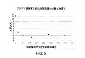
また、ここに提供する様々な実施形態は、二重層によるアプローチにおいて底部保護層の最小厚さを決定するための方法に関し、この厚さは、フィルム全体の電気的特性に対する影響を最小にしながら、基材の酸化に対して十分な保護を提供するような厚さである。 Also, the various embodiments provided herein relate to a method for determining the minimum thickness of the bottom protective layer in a bilayer approach, which thickness minimizes the impact on the overall electrical properties of the film. It is thick enough to provide sufficient protection against oxidation of the substrate.
2011年4月20日に出願された、名称「プラズマ賦活均一フィルム蒸着」の米国特許出願第13/084399号(参照によりその全体を本明細書に援用する)は、基材が反応物A及びBに曝露されるプラズマ賦活CFDプロセスの様々な実施形態のためのタイムチャートを含むCFD反応について記載している。ここで説明される本方法は、こうしたCFDプロセスを含んでいる。以下の説明では主に、ビス(tert−ブチルアミノ)シラン(BTBAS)等のシリコン含有反応物と、酸素、亜酸化窒素又はこれらの混合物等の、酸化反応物としても知られる酸化剤反応物とに由来する酸化シリコンフィルムの蒸着に言及するが、本明細書に記載する本方法は窒化シリコンを含むがこれに限定されない他のタイプのフィルムのプラズマ賦活蒸着にも使用してよい。窒化シリコン及び他のタイプのフィルムの蒸着のための反応物及びプロセスフローは、上記米国特許出願第13/084399号、及び2011年4月11日に出願された、名称「窒化シリコンフィルム及び方法」の米国特許出願第13/084305号(参照によりその全体を本明細書に援用する)に記載されている。 U.S. patent application Ser. No. 13 / 084,399, filed Apr. 20, 2011, entitled "Plasma Activated Uniform Film Deposition" (herein incorporated by reference in its entirety), the substrate comprises Reactant A and B. A CFD response is described that includes time charts for various embodiments of plasma activated CFD processes exposed to B. The method described herein includes such a CFD process. In the following description, mainly, silicon-containing reactants such as bis (tert-butylamino) silane (BTBAS) and oxidant reactants also known as oxidation reactants such as oxygen, nitrous oxide, or a mixture thereof Although the deposition of silicon oxide films derived from the above is mentioned, the method described herein may also be used for plasma activated deposition of other types of films, including but not limited to silicon nitride. Reactants and process flows for the deposition of silicon nitride and other types of films are described in the above-referenced US patent application Ser. No. 13 / 084,399 and filed Apr. 11, 2011, entitled "Silicon Nitride Films and Methods". No. 13 / 084,305, which is hereby incorporated by reference in its entirety.
半導体デバイスの製造は典型的には、統合製造プロセスにおいて非平面基材上に1つ又は複数の薄いフィルムを蒸着することを伴う。この統合プロセスのいくつかの態様では、基材の表面形状に適合する薄いフィルムを蒸着することが有益となり得る。例えば、持ち上げたゲートスタックの上面に窒化シリコンフィルムを蒸着して、低ドープソース及びドレイン領域を後続のイオン注入プロセスから保護するためのスペーサ層として機能させてよい。 Semiconductor device fabrication typically involves depositing one or more thin films on a non-planar substrate in an integrated manufacturing process. In some aspects of this integrated process, it may be beneficial to deposit a thin film that conforms to the surface topography of the substrate. For example, a silicon nitride film may be deposited on top of the lifted gate stack to act as a spacer layer to protect the lightly doped source and drain regions from subsequent ion implantation processes.
スペーサ層蒸着プロセスでは、化学蒸着(CVD)プロセスを用いて非平面基材上に窒化シリコンフィルムを形成してよく、続いてこれに異方性エッチングを施してスペーサ構造を形成する。しかしながら、ゲートスタック間の距離が減少すると、CVDガス相反応の物質輸送限界により、「ブレッドローフィング」蒸着効果が引き起こされ得る。このような効果は典型的には、ゲートスタックの上面の厚い蒸着及びゲートスタックの底部角の薄い蒸着において発生する。更に、デバイスの密度が異なる領域を有するダイが存在し得るため、ウエハ表面にわたる物質輸送効果により、ダイ内及びウエハ内でのフィルムの厚さの変動が引き起こされ得る。これらの厚さの変動により、いくつかの領域でのオーバーエッチング及び他の領域でのアンダーエッチングが発生し得る。これにより、デバイスの性能及び/又はダイの収率が低下し得る。 In the spacer layer deposition process, a chemical vapor deposition (CVD) process may be used to form a silicon nitride film on the non-planar substrate, which is subsequently anisotropically etched to form a spacer structure. However, as the distance between the gate stacks decreases, the mass transport limitations of the CVD gas phase reaction can cause "bread-loafing" deposition effects. Such effects typically occur in thick deposition on top of the gate stack and thin deposition on the bottom corner of the gate stack. Furthermore, because there may be dies with areas of different device density, mass transport effects across the wafer surface may cause film thickness variations within the dies and within the wafer. These thickness variations can cause over-etching in some areas and under-etching in other areas. This can reduce device performance and / or die yield.
これらの問題に対処するためのいくつかの方法は、原子層蒸着(ALD)を伴う。熱で賦活したガス相反応を用いてフィルムを蒸着するCVDプロセスとは対照的に、ALDプロセスは表面媒介蒸着反応を用いて、層毎にフィルムを蒸着する。ある例示的なALDプロセスでは、多数の表面活性部位を含む基材表面を、第1のフィルム前駆物質(P1)のガス相分布に曝露する。P1のいくつかの分子は、基材表面上に、P1の化学吸収種及び物理吸収分子を含む凝集相を形成し得る。続いて反応器を排気してガス相及び物理吸収P1を除去し、化学吸収種のみを残す。次に第2のフィルム前駆物質(P2)を反応器に導入し、P2のいくつかの分子を基材表面に吸収させる。反応器を再び排気して、今度は結合していないP2を除去することができる。その後、基材に供給される熱エネルギが、P1及びP2の吸収された分子間の表面反応を賦活し、フィルム層を形成する。最後に、反応器を排気して副産物並びに場合によっては未反応のP1及びP2を除去し、ALDサイクルを終了する。フィルムの厚みを形成するために、追加のALDサイクルを含んでもよい。 Several methods to address these issues involve atomic layer deposition (ALD). In contrast to CVD processes that deposit films using thermally activated gas phase reactions, ALD processes use surface-mediated deposition reactions to deposit film layer by layer. In one exemplary ALD process, a substrate surface comprising a number of surface active sites is exposed to the gas phase distribution of a first film precursor (P1). Several molecules of P1 can form an aggregated phase comprising a chemisorbed species of P1 and physically absorbable molecules on the substrate surface. The reactor is subsequently vented to remove gas phase and physical absorption P1, leaving only chemisorbed species. A second film precursor (P2) is then introduced into the reactor to allow some molecules of P2 to be absorbed onto the substrate surface. The reactor can be evacuated again to remove unbound P2 this time. The thermal energy supplied to the substrate then activates the surface reaction between the absorbed molecules of P1 and P2 to form a film layer. Finally, the reactor is vented to remove byproducts and possibly unreacted P1 and P2 and complete the ALD cycle. Additional ALD cycles may be included to form the thickness of the film.
前駆物質ドープステップの曝露時間及び前駆物質の付着係数に応じて、各ALDサイクルによって例えば1/3〜1/2Åの厚さのフィルム層を蒸着できる。 Depending on the exposure time of the precursor doping step and the deposition coefficient of the precursor, each ALD cycle can deposit a film layer of, for example, a thickness of 1/3 to 1/2 Å.
平面基材上に均一フィルムを蒸着することもできる。例えば、交互になったタイプのフィルムからなる平面のスタックから、リソグラフィのパターニングにおける応用のための反射防止層を形成できる。このような反射防止層の厚さは約100〜1000Åであり得、これは迅速なCVDプロセスに比べて、遅いALDプロセスの魅力を損なう。しかしながら、このような反射防止層はウエハ内での厚さの変動に関して、多くのCVDプロセスが提供できる許容誤差よりも低い許容誤差を有することもできる。例えば、厚さ600Åの反射防止層は、厚さに関して3Å未満の範囲の許容誤差を有し得る。 Uniform films can also be deposited on planar substrates. For example, a planar stack of alternating type films can form an antireflective layer for applications in lithographic patterning. The thickness of such an antireflective layer may be about 100-1000 Å, which impairs the appeal of slow ALD processes compared to rapid CVD processes. However, such antireflective layers can also have tolerances that are less than the tolerances that many CVD processes can provide with respect to thickness variations within the wafer. For example, a 600 Å thick antireflective layer may have a tolerance in the range of less than 3 Å with respect to thickness.
非平面及び平面基材上でのプラズマ賦活ALD及び均一フィルム蒸着(CFD)のためのプロセス及び設備を提供する様々な実施形態をここで提供する。これらの実施形態は典型的には、比較的低温及び/又は比較的低圧及び/又は比較的低いRF電力/束レベル(即ち低損傷条件)で実施される。場合によっては、二重層によるアプローチを用いて、底部保護層を低損傷条件で形成し、上部電気的に有利な層を異なる条件で形成する。 Various embodiments are provided herein that provide processes and equipment for plasma activated ALD and uniform film deposition (CFD) on non-planar and planar substrates. These embodiments are typically implemented at relatively low temperature and / or relatively low pressure and / or relatively low RF power / bundle levels (i.e., low damage conditions). In some cases, using a double layer approach, the bottom protective layer is formed at low damage conditions and the top electrically advantageous layer is formed at different conditions.
上に示したように、本明細書に記載する実施形態はCFDプロセス及びALDプロセスを含むことができる。一般にCFDプロセスプロセスは、フィルムを形成する反応の前の1つ又は複数の反応物の完全なパージを必要としない。例えば、プラズマ(又はその他の賦活エネルギ)を投入する際に1つ又は複数の反応物が気相で存在してよい。従って、ALDプロセスで説明するプロセスステップのうち1つ又は複数は、例示的なCFDプロセスでは短縮又は削除してよい。更に、いくつかの実施形態では、蒸着反応のプラズマ賦活により、蒸着温度を熱賦活反応よりも低くすることができ、一体プロセスの熱収支を潜在的に低減する。実施形態はCFDを含むが、本明細書に記載する本方法はCFDに限定されない。他の適切な方法として、ALDが挙げられる。 As indicated above, the embodiments described herein can include CFD processes and ALD processes. In general, the CFD process does not require a complete purge of one or more reactants prior to the film forming reaction. For example, one or more reactants may be present in the gas phase upon introduction of plasma (or other activation energy). Thus, one or more of the process steps described in the ALD process may be shortened or eliminated in the exemplary CFD process. Furthermore, in some embodiments, plasma activation of the deposition reaction may allow the deposition temperature to be lower than the thermal activation reaction, potentially reducing the thermal budget of the integral process. Embodiments include CFD, but the methods described herein are not limited to CFD. Another suitable method is ALD.
文脈上、CFDに関して簡単に説明する。CFD「サイクル」という概念は、様々な実施形態に関するここでの議論に関係する。一般にサイクルは、表面蒸着反応を1回実施するために必要な最小の組の操作を意味する。1サイクルの結果、基材表面上に少なくとも部分的なフィルム層が生成される。典型的にはCFDサイクルは、基材表面に各反応物を送達して吸収させ、その後これら吸収された反応物を反応させてフィルムの部分層を形成するために必要なステップのみを含む。当然のことであるが、サイクルは、反応物若しくは副産物のうちの1つ若しくは複数を排出するステップ及び/又は蒸着されたままの状態の部分フィルムを処理するステップ等、特定の補助的なステップを含んでよい。サイクルは一般に、操作の一意の順序を1例のみ含む。例として、サイクルは以下の操作を含んでよい:(i)反応物Aの送達/吸収;(ii)反応物Bの送達/吸収;(iii)反応物Bを反応チャンバの外へと排出する;及び(iv)プラズマを適用してAとBとの表面反応を駆動し、表面上に部分的なフィルム層を形成する。 In context, we will briefly describe CFD. The notion of a CFD "cycle" relates to the discussion herein of various embodiments. In general, cycle refers to the minimum set of operations required to perform a surface deposition reaction once. One cycle results in the production of at least a partial film layer on the substrate surface. Typically, the CFD cycle involves only the steps necessary to deliver and absorb each reactant to the substrate surface and then react the absorbed reactants to form a partial layer of film. It will be appreciated that the cycle includes certain additional steps, such as discharging one or more of the reactants or byproducts and / or treating the partial film as deposited. May be included. A cycle generally contains only one unique sequence of operations. As an example, the cycle may include the following operations: (i) Delivery / Absorption of Reactant A; (ii) Delivery / Absorption of Reactant B; (iii) Discharge Reactant B out of the reaction chamber And (iv) applying a plasma to drive the surface reaction of A and B to form a partial film layer on the surface.
ここでの説明には、「主」及び「副」反応物という用語を使用する。主反応物は室温で固体である要素を含み、この要素はCFDで形成されるフィルムを形成する。このような要素の例は、金属(例えばアルミニウム、チタン等)、半導体(例えばシリコン及びゲルマニウム)及び非金属又は半金属(例えばホウ素)である。副反応物は主反応物でないいずれの反応物である。副反応物を指して用語「共反応物」を使用することがある。副反応物の例としては、酸素、オゾン、水素、炭素、一酸化物、亜酸化窒素、アンモニア、アルキルアミン等が挙げられる。 The terms "primary" and "secondary" reactants are used in the description herein. The main reactant comprises an element that is solid at room temperature, which forms a film formed by CFD. Examples of such elements are metals (e.g. aluminum, titanium etc.), semiconductors (e.g. silicon and germanium) and nonmetals or semimetals (e.g. boron). By-products are any reactants that are not the main reactant. The term "co-reactant" may be used to refer to side reactions. Examples of by-products include oxygen, ozone, hydrogen, carbon, monoxide, nitrous oxide, ammonia, alkylamine and the like.
本明細書に記載する実施形態では、様々な異なるプロセスの順序を使用してよい。1つの可能なプロセスは、以下の操作順序を含む:(1)副反応物を連続的に流す;(2)1用量のシリコン含有反応物又は他の主反応物を提供する;(3)1をパージする;(4)基材をRFプラズマに曝露する;(5)2をパージする。別の代替プロセスは、以下の操作順序を含む:(1)不活性ガスを連続的に流す;(2)1用量のシリコン含有反応物又は他の主反応物を提供する;(3)1をパージする;(4)1用量の酸化剤又はその他の副反応物を提供しながら、基材をRFプラズマに曝露する;(5)2をパージする。他の例示的なプロセスフローを図1A〜1Eに示す。 A variety of different process sequences may be used in the embodiments described herein. One possible process involves the following operating sequence: (1) flushing side reactions continuously; (2) providing one dose of silicon containing reactant or other main reactant; (3) 1 (4) expose the substrate to an RF plasma; (5) purge the 2; Another alternative process involves the following sequence of operations: (1) flowing an inert gas continuously; (2) providing a dose of silicon containing reactant or other main reactant; (3) 1 Purge; (4) expose substrate to RF plasma while providing one dose of oxidant or other by-products; (5) purge 2. Another exemplary process flow is shown in FIGS. 1A-1E.
ここに示す化合物、流量及び注入時間は例である。酸化シリコンの蒸着のために、適切ないずれのシリコン含有反応物及び酸化剤を用いてもよい。同様に、窒化シリコンの蒸着のために、適切ないずれのシリコン含有反応物及び窒素含有反応物を用いてもよい。更に、酸化金属又は窒化金属の蒸着のために、適切ないずれの金属含有反応物及び共反応物を用いてもよい。本技術は、幅広い化学的性質のフィルムを実装するにあたって有益である。上に挙げた範囲の外の流量及び時間も、特定の実施形態には適切であり得る。例示的な流量は300mmのウエハに関するものであり、他のサイズのウエハに関しては適宜調整してよい。他のプロセスフローも使用でき、そのうちの幾つかを図1A及び1Bに示すタイムチャートを参照して以下に説明する。 The compounds, flow rates and infusion times shown here are examples. Any suitable silicon-containing reactant and oxidizing agent may be used to deposit silicon oxide. Similarly, any suitable silicon-containing and nitrogen-containing reactants may be used to deposit silicon nitride. Furthermore, any metal-containing reactant and co-reactant suitable for metal oxide or metal nitride deposition may be used. The technology is useful in implementing films of a wide range of chemistries. Flow rates and times outside of the ranges listed above may also be appropriate for particular embodiments. Exemplary flow rates are for 300 mm wafers and may be adjusted as appropriate for other sized wafers. Other process flows can also be used, some of which are described below with reference to the time charts shown in FIGS. 1A and 1B.
場合によっては、反応物のうちの1つを連続的に(例えば他の反応物の送達中及び/又はプラズマ曝露中でさえ)送達してよい。連続的に流れる反応物を、例えばアルゴン等のキャリアガスと併せて反応チャンバに送達してよい。場合によっては、連続的に流れる反応物の反応チャンバへの送達は、方向切替弁/流入弁のトグリングを用いて制御できる。気体流の変更は、方向を変えるか又は並行流としてよい。ある例では、連続的に流れる反応物は、特定の期間のみ反応チャンバに送達されるよう、反応チャンバから周期的に方向を切り替えてよい。連続的に流れるガスは、適切なバルブを用いて流出口/集積場へと方向を切り替えてよい。例えば、酸化反応物は連続的に流れてよいが、反応チャンバには周期的にのみ送達される。酸化反応物が反応チャンバに送達されない場合、酸化反応物は流出口、再利用システム等へと方向を切り替えてよい。 In some cases, one of the reactants may be delivered continuously (eg, during delivery of the other reactant and / or even during plasma exposure). The continuously flowing reactant may be delivered to the reaction chamber in conjunction with a carrier gas such as, for example, argon. In some cases, delivery of continuously flowing reactants to the reaction chamber can be controlled using toggling of the diverter valve / inlet valve. The change of gas flow may be diverted or in parallel. In one example, continuously flowing reactants may be periodically diverted from the reaction chamber to be delivered to the reaction chamber only for a specific period of time. Continuously flowing gas may be diverted to the outlet / accumulation site using appropriate valves. For example, the oxidation reactant may flow continuously but is only delivered periodically to the reaction chamber. If the oxidation reactant is not delivered to the reaction chamber, the oxidation reactant may switch direction to the outlet, recycle system, etc.
連続した流れの実施形態の1つの利点は、確立された流れによって、流れのオン及びオフの転換に関連する瞬間的な初期化及び安定化によって発生する遅延及び流れの変動が回避されることである。 One advantage of the continuous flow embodiment is that the established flow avoids the delay and flow variations caused by the instantaneous initialization and stabilization associated with the flow on and off transitions. is there.
具体的な実施例として、主反応物(「固体成分」前駆物質、又はこの例では単に「反応物B」と呼ぶ場合もある)を用いて、酸化物フィルムを均一フィルム蒸着プロセスによって蒸着してよい。ビス(tert−ブチルアミノ)シラン(BTBAS)は、このような主反応物の1つである。この実施例では、酸化物蒸着プロセスは、酸素又は亜酸化窒素等の酸化剤の送達を伴い、酸化剤はそれぞれの曝露段階において、主反応物の送達中に最初から及び連続的に流れる。酸化剤はまた、それぞれのプラズマ曝露段階中も流れ続ける。例えば図1Aに示す順序を参照のこと。 As a specific example, an oxide film is deposited by a uniform film deposition process using a main reactant ("solid component" precursor, or sometimes referred to simply as "reactant B" in this example) Good. Bis (tert-butylamino) silane (BTBAS) is one such main reactant. In this example, the oxide deposition process involves the delivery of an oxidizing agent such as oxygen or nitrous oxide, and the oxidizing agent flows from the beginning and continuously during delivery of the main reactant at each exposure stage. The oxidant also continues to flow during each plasma exposure stage. See, for example, the order shown in FIG. 1A.
いくつかの具体的な実施例では、連続的に流れる反応物は副反応物である。連続的に流れる反応物は、一定の流量又は変動するが制御された流量で供給してよい。後者の場合、例として、副反応物の流量は主反応物が送達される際の曝露段階中は低下し得る。例えば、酸化物蒸着において、酸化剤(例えば酸素又は亜酸化窒素)は全蒸着シーケンス中連続的に流れてよいが、その流量は主反応物(例えばBTBAS)が送達される際に低下し得る。これにより、BTBASの分圧はその注入中に増大し、これによって基材表面を飽和させるために必要な曝露時間が短くなる。プラズマを着火する直前に、酸化剤の流れを増大させて、プラズマ曝露段階中にBTBASが存在する可能性を低減させてよい。いくつかの実施形態では、連続的に流れる反応物は、2回以上の蒸着サイクルの過程全体にわたって、変動する流量で流れる。例えば反応物は、第1のCFDサイクル中は第1の流量で流れ、第2のCFDサイクル中は第2の流量で流れてよい。様々な実施形態では、反応サイクルの第1のセットを特定の蒸着条件下で実施し、その後反応サイクルの第2のセットを異なる条件下で実施して、第1のフィルム上に第2のフィルムを蒸着する。これら2つのフィルムは異なる特性を有してよく;例えば第2のフィルムは、所望の応用例に関してより電気的に有利な特性を有する。 In some specific embodiments, the continuously flowing reactant is a side reactant. The continuously flowing reactant may be supplied at a constant flow rate or at a fluctuating but controlled flow rate. In the latter case, as an example, the flow rate of the side reactant can be reduced during the exposure phase when the main reactant is delivered. For example, in oxide deposition, the oxidant (eg, oxygen or nitrous oxide) may flow continuously throughout the deposition sequence, but its flow rate may decrease as the main reactant (eg, BTBAS) is delivered. This causes the BTBAS partial pressure to increase during its injection, which reduces the exposure time required to saturate the substrate surface. Just prior to igniting the plasma, the oxidant flow may be increased to reduce the possibility of BTBAS being present during the plasma exposure phase. In some embodiments, the continuously flowing reactant flows at varying flow rates throughout the course of two or more deposition cycles. For example, the reactants may flow at a first flow rate during a first CFD cycle and at a second flow rate during a second CFD cycle. In various embodiments, a first set of reaction cycles is performed under specific deposition conditions, and then a second set of reaction cycles is performed under different conditions to produce a second film on the first film. Deposit. These two films may have different properties; for example, the second film has more electrically advantageous properties for the desired application.
複数の副反応物を用いる場合、反応チャンバへの送達の前にこれらを混合するか、又は別個の流れとして送達できる。いくつかの実施形態では、副反応物を、パージ操作のためのバーナーに送達される不活性ガス流と共に連続的に送達する。いくつかの実施形態では、不活性ガス流は、パージ操作のために不活性ガス流量を増大させて又は増大させることなく、連続的であってよい。プラズマが消えた後に更なるパージが発生し得る。 If multiple side reactions are used, they can be mixed prior to delivery to the reaction chamber or delivered as separate streams. In some embodiments, the side reactants are delivered continuously with the inert gas stream delivered to the burner for the purge operation. In some embodiments, the inert gas flow may be continuous without increasing or increasing the inert gas flow rate for the purge operation. A further purge can occur after the plasma has extinguished.
CFD「排出」又は「パージ」ステップ又は段階という概念について、ここで様々な実施形態において議論する。一般に排出段階は、反応チャンバから気相反応物の1つを除去又はパージし、典型的にはこれは当該反応物の送達が完了した直後に起こる。言い換えると、排出段階中には反応物はもはや反応チャンバに送達されない。しかしながら、排出段階中、反応物は基材表面に吸収されたままである。典型的には、この排出は、反応物が基材表面に所望のレベルまで吸収された後に、チャンバ内のいずれの残留気相反応物も除去する役割を果たす。排出段階はまた、吸収が弱い種(例えば、特定の前駆物質リガンド又は反応副産物)を基材表面から除去してもよい。ALDにおいて、排出段階は、2つの反応物のガス相相互作用、又は1つの反応物と、熱、プラズマ、若しくは表面反応のための他の駆動力との相互作用を防ぐために必要なものと考えられてきた。一般に、及びそうでなければここに明示するように、排出/パージ段階は(i)反応チャンバを排気する、及び/又は(ii)排出される種を含まないガスを、反応チャンバを通して流すことで達成できる。(ii)の場合、このようなガスは例えば不活性ガス、又は連続的に流れる副反応物等の副反応物であってよい。 The concept of a CFD "discharge" or "purge" step or stage is discussed herein in various embodiments. In general, the evacuation phase removes or purges one of the gas phase reactants from the reaction chamber, which typically occurs immediately after delivery of the reactants is complete. In other words, reactants are no longer delivered to the reaction chamber during the evacuation phase. However, during the discharge phase, the reactants remain absorbed on the substrate surface. Typically, this discharge serves to remove any residual gas phase reactants in the chamber after the reactants are absorbed to the desired level on the substrate surface. The ejection step may also remove weakly absorbing species (e.g., certain precursor ligands or reaction byproducts) from the substrate surface. In ALD, the evacuation step is considered as necessary to prevent the gas phase interaction of two reactants, or the interaction of one reactant with heat, plasma, or other driving forces for surface reactions. It has been In general, and as otherwise specified herein, the evacuation / purge phase is (i) evacuating the reaction chamber, and / or (ii) flowing a species free gas through the reaction chamber. Can be achieved. In the case of (ii), such a gas may be, for example, an inert gas or a side reactant such as a continuously flowing side reactant.
様々な実施形態は、異なる時点に排出段階を実装してよい。例えば特定の場合には、排出ステップは以下のいずれの時点に発生してもよい:(1)主反応物の送達後;(2)主反応物を送達するパルスの間;(3)副反応物の送達後;(4)プラズマ曝露の前;(5)プラズマ曝露の後;及び(6)(1)〜(5)のいずれの組合せ。これらの時間フレームのうちのいくつかは重複し得る。主反応物の送達後に実施される第1の排出、及びプラズマ励起後に実施される第2の排出は、均一なフィルムを蒸着するにあたって特に有益であることが分かった。 Various embodiments may implement the draining stage at different times. For example, in certain cases, the draining step may occur at any of the following times: (1) after delivery of the main reactant; (2) during the pulse of delivering the main reactant; (3) side reactions (4) before plasma exposure; (5) after plasma exposure; and (6) any combination of (1) to (5). Some of these time frames may overlap. A first discharge performed after delivery of the main reactant and a second discharge performed after plasma excitation have been found to be particularly useful in depositing uniform films.
他の多数の蒸着プロセス、特にこれらが必要とする熱賦活とは違って、CFDプロセスは比較的低温で実施できる。一般にCFD温度は約20〜400℃となる。この温度を選択して、フォトレジストコア上への蒸着等の温度感受性プロセスでの蒸着を可能とすることができる。特定の実施形態では、約20〜100℃の温度を用いてダブルパターニングの応用を行う(例えばフォトレジストコアを使用)。別の実施形態では、約200〜350℃の温度を用いてメモリ製造処理を行う。いくつかの実装形態では、反応サイクルの第1のセットを第1の温度で実施し、反応サイクルの第2のセットを第1の温度より高い第2の温度で実施する。 Unlike many other deposition processes, especially the thermal activation that they require, the CFD process can be performed at relatively low temperatures. Generally, the CFD temperature will be about 20-400 ° C. This temperature can be selected to enable deposition in a temperature sensitive process such as deposition on a photoresist core. In particular embodiments, temperatures of about 20-100 ° C. are used to apply double patterning (eg, using a photoresist core). In another embodiment, the memory fabrication process is performed using a temperature of about 200-350.degree. In some implementations, a first set of reaction cycles is performed at a first temperature, and a second set of reaction cycles is performed at a second temperature higher than the first temperature.
上で提案したように、CFDは先進技術のノードにおいてフィルムを蒸着するのによく適している。よって例えば、CFD処理を32nmノード、22nmノード、16nmノード、11nmノード、及びこれらのいずれでもないノードにおけるプロセスに適用できる。これらのノードについては、長年に渡るマイクロエレクトロニクス技術の要件に関する産業上の同意である、国際半導体技術ロードマップ(ITRS)に記載されている。これは一般にハーフピッチのメモリセルを基準とする。具体的な実施例では、CFD処理は「2X」デバイス(20〜29nmの範囲のデバイス特徴部分を有する)及びそれ以上のものに適用される。 As suggested above, CFD is well suited to depositing films at advanced technology nodes. Thus, for example, CFD processing can be applied to processes at the 32 nm node, 22 nm node, 16 nm node, 11 nm node, and nodes other than these. These nodes are described in the International Semiconductor Technology Roadmap (ITRS), an industry agreement on the requirements of microelectronics for many years. This is generally based on half pitch memory cells. In a specific embodiment, CFD processing is applied to "2X" devices (with device features in the range of 20-29 nm) and more.
ここで提示するCFDフィルムの大半の例は、シリコン系マイクロエレクトロニクスデバイスに関するものであるが、このフィルムを他の領域において応用することもできる。GaAs及び他のIII−V半導体等の非シリコン半導体、並びにHgCdTe等のII−VI材料を用いるマイクロエレクトロニクス又はオプトエレクトロニクスは、ここに開示するCFDプロセスを用いることにより利益を得ることができる。光電池デバイス等の太陽エネルギの分野、電気着色の分野及びその他の分野における均一絶縁フィルムの応用も可能である。 Most examples of CFD films presented here relate to silicon-based microelectronic devices, but the films can also be applied in other areas. Microelectronics or optoelectronics using non-silicon semiconductors such as GaAs and other III-V semiconductors and II-VI materials such as HgCdTe can benefit from using the CFD process disclosed herein. The application of uniform insulating films in the field of solar energy such as photovoltaic devices, in the field of electro-coloring and other fields is also possible.
CFDフィルムの他の例示的応用は、ラインの後端の相互接続分離のための応用における均一低kフィルム(例えばいくつかの比限定的な例では約3.0以下のk)、エッチング停止及びスペーサ層への応用のための均一窒化シリコンフィルム、均一反射防止層、並びに銅付着及び防護層を含むがこれらに限定されない。BEOL処理のための低k絶縁体の多くの異なる組成を、CFDを用いて製造できる。例としては酸化シリコン、酸素ドープカーバイド、炭素ドープ酸化物、酸窒化物等が挙げられる。 Other exemplary applications of CFD films include uniform low-k films (eg, k of about 3.0 or less in some non-limiting examples), etch stop and in applications for interconnect separation at the back end of lines These include, but are not limited to, uniform silicon nitride films for applications to spacer layers, uniform antireflective layers, and copper adhesion and protective layers. Many different compositions of low k insulators for BEOL processing can be manufactured using CFD. Examples include silicon oxide, oxygen-doped carbide, carbon-doped oxide, oxynitride and the like.
図1Aは、プラズマ賦活CFDプロセスの例示的実施形態のためのタイムチャート100を概略的に示す。2回の完全なCFDサイクルを示す。図示したように、各CFDサイクルサイクルは、反応物Aへの曝露段階120、その直後に続く反応物Bへの曝露段階140、反応物Bの排出段階160、及び最後にプラズマ賦活段階180を含む。プラズマ賦活段階180A及び180Bのプロセス中にもたらされるプラズマエネルギは、表面吸収反応物種AとBとの間の反応を賦活する。図示した実施形態では、一方の反応物(反応物A)が送達された後には排出段階は実施されない。実際、この反応物はフィルム蒸着プロセス中は連続的に流れる。よって、反応物Aがガス相であるときにプラズマが着火される。図示した実施形態では、反応物ガスA及びBは反応しないままガス相で共存してよい。従って、ALDプロセスにおいて記載したプロセスステップのうちの1つ又は複数を、この例示的なCFDプロセスでは短縮又は削除してよい。例えばA曝露段階120A及び120Bの後の排出ステップは削除してよい。 FIG. 1A schematically illustrates a
図1Aはまた、様々なCFDプロセスパラメータに関する、例示的なCFDプロセス段階の時間経過も示す。図1Aは2つの例示的な蒸着サイクル110A及び110Bを示すが、所望の厚さのフィルムを蒸着するために、CFDプロセスにはいずれの適切な回数の蒸着サイクルを含んでもよいことを理解されたい。例示的CFDプロセスパラメータは、不活性種及び反応物種の流量、プラズマ電力及びプラズマ周波数、基材温度、並びにプロセスステーション圧力を含むがこれらに限定されない。 FIG. 1A also shows the time course of exemplary CFD process steps for various CFD process parameters. Although FIG. 1A shows two exemplary deposition cycles 110A and 110B, it should be understood that the CFD process may include any suitable number of deposition cycles to deposit a film of the desired thickness. . Exemplary CFD process parameters include, but are not limited to, flow rates of inert species and reactant species, plasma power and plasma frequency, substrate temperature, and process station pressure.
CFDサイクルは典型的には、各反応物に対する曝露段階を含む。この「曝露段階」の間、反応物はプロセスチャンバに送達され、基材表面上への反応物の吸収が起こる。典型的には、曝露段階の開始時において、基材表面は認識可能な反応物の吸収量を全く有さない。図1Aでは、反応物A曝露段階120A及びBにおいて、反応物Aは制御された流量でプロセスステーションに供給され、基材の曝露表面を飽和させる。反応物Aはいずれの適切な蒸着反応物であってもよく;例えば主反応物又は副反応物であってよい。CFDが二酸化シリコンフィルムを生成する実施例では、反応物Aは酸素であってよい。 The CFD cycle typically includes an exposure step for each reactant. During this "exposure phase", the reactants are delivered to the process chamber and absorption of the reactants onto the substrate surface takes place. Typically, at the beginning of the exposure phase, the substrate surface has no discernible reactant absorption. In FIG. 1A, in reactant A exposure stages 120A and B, reactant A is supplied to the process station at a controlled flow rate to saturate the exposed surface of the substrate. Reactant A may be any suitable vapor deposition reactant; for example, a main reactant or a side reactant. In embodiments where CFD produces a silicon dioxide film, reactant A may be oxygen.
図1Aに示す実施形態では、反応物Aは蒸着サイクル110A及び110B全体を通して連続的に流れる。ガス相の反応を防ぐためにフィルム前駆物質の曝露が分離されている典型的なALDプロセスとは異なり、反応物A及びBは、CFDプロセスのいくつかの実施形態のガス相において混合できる。上で示したように、いくつかの実施形態では反応物A及びBを、プラズマエネルギの印加又は表面反応の賦活の前に、反応器内にある条件下で互いに明らかな反応を起こさないままガス相で共存できるよう、選択する。場合によっては、反応物は(1)これらの間の反応が熱力学的に有利(即ちギブズ自由エネルギ<0)であるよう、及び(2)反応が、所望の蒸着温度においてプラズマ励起がなければ無視できる反応しか起こらないような十分に高い賦活エネルギを有するよう、選択される。 In the embodiment shown in FIG. 1A, reactant A flows continuously throughout the deposition cycle 110A and 110B. Unlike a typical ALD process where exposure of film precursors is separated to prevent reaction of the gas phase, reactants A and B can be mixed in the gas phase of some embodiments of the CFD process. As indicated above, in some embodiments, Reactants A and B are gases that do not undergo appreciable reaction with each other under conditions in the reactor prior to application of plasma energy or activation of the surface reaction. Choose to be able to co-exist in phase. In some cases, the reactants are (1) such that the reaction between them is thermodynamically favorable (ie, Gibbs free energy <0), and (2) the reaction is not plasma excited at the desired deposition temperature. It is chosen to have a sufficiently high activation energy such that only negligible reaction occurs.
プロセスステーションに反応物Aを連続的に供給することにより、初めに反応物Aの供給を開始し、続いて安定化させて基材を曝露し、その後供給を止め、最後に反応器から除去するALDプロセスに比べて、反応物Aの流量の供給開始及び安定化時間を削減又は削除できる。図1Aに示す実施形態は、一定の流量を有するものとして反応物A曝露段階120A及びBを示しているが、本開示の範囲内において、可変流を含むいずれの適切な反応物Aの流れも使用してよいことを理解されたい。更に、図1Aは全CFDサイクル(蒸着サイクル110A)中に一定の流量を有する反応物Aを示すが、これは必ずしもそうでなくてよい。例えば、反応物Aの流量はB曝露段階140A及び140Gの間に減少してよい。これにより、Bの分圧が増大し、従って反応物Bを基材表面に吸収する駆動力も増大し得る。他の場合には、反応物A及びBはそれぞれ1用量ずつ送達してよい(即ちいずれの反応物も連続的に流れない)。 Start the feed of reactant A first by continuously feeding reactant A to the process station, then stabilize to expose the substrate, then stop the feed and finally remove it from the reactor As compared to the ALD process, the initiation and stabilization time of the reactant A flow rate can be reduced or eliminated. The embodiment shown in FIG. 1A shows reactant A exposure stages 120A and B as having a constant flow rate, but any suitable reactant A stream, including variable flow, is within the scope of the present disclosure. Please understand that it is good to use. Furthermore, although FIG. 1A shows reactant A having a constant flow rate during the entire CFD cycle (deposition cycle 110A), this may not necessarily be the case. For example, the flow rate of reactant A may decrease between B exposure stages 140A and 140G. This may increase the partial pressure of B and thus also the driving force for absorbing reactant B on the substrate surface. In other cases, Reactants A and B may be delivered one dose each (i.e. none of the reactants flow continuously).
いくつかの実施形態では、反応物A曝露段階120Aは、反応物Aに関する基材表面飽和時間を超える長さを有する。例えば、図1Aの実施形態は反応物A曝露段階120Aに、飽和後曝露時間130を含む。任意に、反応物A曝露段階120Aは不活性ガスの制御された流量を含む。例示的な不活性ガスは、窒素、アルゴン及びヘリウムを含むがこれらに限定されない。不活性ガスは、プロセスステーションの圧力並びに/又は温度制御、液状前駆物質の蒸発、前駆物質並びに/又はプロセスガスをプロセスステーション及び/若しくはプロセスステーション配管から除去するための排出ガスのより迅速な送達を補助するために提供してよい。 In some embodiments, reactant
図1Aに示す実施形態の反応物B曝露段階140Aにおいて、反応物Bは制御された流量でプロセスステーションに供給され、曝露された基材表面を飽和させる。ある例示的な二酸化シリコンフィルムでは、反応物BはBTBASであってよい。図1Aの実施形態は、一定の流量を有するものとして反応物B曝露段階140Aを示しているが、本開示の範囲内において、可変流を含むいずれの適切な反応物Bの流れも使用してよいことを理解されたい。更に、反応物B曝露段階140Aはいずれの適切な長さも有してよいことを理解されたい。いくつかの実施形態では、反応物B曝露段階140Aは、反応物Bに関する基材表面飽和時間を超える長さを有してよい。例えば、図1Aに示す実施形態は、反応物B曝露段階140Aに、飽和後曝露時間150を含む。任意に、反応物B曝露段階140Aは適切な不活性ガスの制御された流れを含んでよく、この不活性ガスは上述のように、プロセスステーションの圧力並びに/又は温度制御、液状前駆物質の蒸発、前駆物質のより迅速な送達を補助でき、プロセスステーションガスの逆拡散を防げる。 In reactant
図1Aに示すCFDプロセスの実施形態ではプラズマで賦活されるが、本開示の範囲内において、他の非熱エネルギ源を用いてよい。非熱エネルギ源の非限定的な例は、紫外線ランプ、下流又は遠隔プラズマ源、容量結合プラズマ、誘導結合プラズマ及びマイクロ波表面波プラズマを含むがこれらに限定されない。 Although the embodiment of the CFD process shown in FIG. 1A is plasma activated, other non-thermal energy sources may be used within the scope of the present disclosure. Non-limiting examples of non-thermal energy sources include, but are not limited to, ultraviolet lamps, downstream or remote plasma sources, capacitively coupled plasmas, inductively coupled plasmas and microwave surface wave plasmas.
いくつかのシナリオでは、表面吸収B種は基材表面上に不連続な島として存在してよく、これによって反応物Bの表面飽和を達成するのが困難になる。様々な表面条件により、基材表面上での反応物Bの核生成及び飽和が遅延され得る。例えば、反応物A及び/又はBの吸収によって放出されるリガンドはいくつかの表面活性部位をブロックして、反応物Bの更なる吸収を防ぐことができる。従っていくつかの実施形態では、反応物Bの連続的な吸収層は、反応物Bの流れ及び/又はプロセスステーションへの別個のパルス状の反応物Bを、反応物B曝露段階140A中に変調することにより提供できる。これにより、一定の流れのシナリオと比較して、反応物Bの消費を抑えながら表面吸収及び脱離プロセスのための余剰の時間を提供できる。 In some scenarios, surface absorbed B species may be present as discrete islands on the substrate surface, which makes it difficult to achieve surface saturation of reactant B. Various surface conditions can delay nucleation and saturation of reactant B on the substrate surface. For example, ligands released by absorption of reactants A and / or B can block some surface active sites to prevent further absorption of reactant B. Thus, in some embodiments, the continuous absorbing layer of Reactant B modulates the reactant B stream and / or the separate pulsed Reactant B to the process station during Reactant
更に又は代わりに、いくつかの実施形態では、反応物Bの連続的な曝露の間に、1回又は複数回の排出段階を含んでよい。例えば図1Bの実施形態は、蒸着サイクル210のための例示的なCFDプロセスのタイムチャート200を概略的に示す。反応物B曝露段階240Aにおいて、反応物Bに基材表面を曝露する。続いて排出段階260Aにおいて、反応物Bの供給を止め、反応物Bのガス相種をプロセスステーションから除去する。あるシナリオでは、ガス相の反応物Bを反応物A及び/又は不活性ガスの連続的な流れで置換してよい。別のシナリオでは、プロセスステーションを排気することによってガス相の反応物Bを除去してよい。ガス相の反応物Bの除去により、吸収/脱離プロセスの平衡をシフトしてリガンドを脱離させ、吸収されたBの表面再構成を促進して吸収されたBの不連続な島を統合できる。反応物B曝露段階240Bにおいて、反応物Bに基材表面を再び曝露する。図1Bに示す実施形態は1回の反応物B排出及び曝露サイクルを含むが、本開示の範囲内において、いずれの適切な回数においても交互の排出及び曝露サイクルの繰り返しを使用できることを理解されたい。 Additionally or alternatively, in some embodiments, during continuous exposure of Reactant B, one or more evacuation steps may be included. For example, the embodiment of FIG. 1B schematically illustrates a
ここで図1Aの実施形態に戻ると、180Aにおいてプラズマによって賦活する前に、いくつかの実施形態では、排出段階160Aにおいてガス相の反応物Bをプロセスステーションから除去してよい。CFDサイクルは上述の曝露段階に加えて、1回又は複数回の排出段階を含んでよい。プロセスステーションを排出させることにより、反応物Bがプラズマ賦活の影響を受けやすいガス相反応を回避できる。更に、プロセスステーションを排出させることにより、残留してフィルムを汚染し得る表面吸収リガンドを除去できる。例示的な排出ガスは、アルゴン、ヘリウム及び窒素を含むがこれらに限定されない。図1Aに示す実施形態では、排出段階160Aのための排出ガスは不活性ガス流により供給される。いくつかの実施形態では、排出段階160Aはプロセスステーションを廃棄するための1回又は複数の排気サブ段階を含んでよい。代替として、いくつかの実施形態では、排出段階160Aを省略してもよいことを理解されたい。 Returning now to the embodiment of FIG. 1A, in some embodiments, reactant B in the gas phase may be removed from the process station in
排出段階160Aはいずれの適切な長さを有してよい。いくつかの実施形態では、1つ又は複数の排出ガスの流量を増加することにより、排出段階160Aの長さを短縮できる。例えば、排出段階160Aの長さを変更するために、排出ガスの流量を、反応物の様々な熱力学的特性並びに/又はプロセスステーション及び/若しくはプロセスステーションの配管の幾何学的特性に応じて調整してよい。ある非限定的な例では、排出段階の長さは排出ガス流量の調整によって最適化してよい。これにより蒸着サイクルの時間を短縮でき、基材のスループットを改善できる。
CFDサイクルは典型的には、上述の曝露段階及び任意の排出段階に加えて「賦活段階」を含む。賦活段階は、基材表面に吸収された1つ又は複数の反応物の反応を駆動する役割を果たす。図1Aに示す実施例のプラズマ賦活段階180Aにおいて、プラズマエネルギを供給して、表面吸収反応物AとBとの間の表面反応を賦活する。例えば、プラズマは反応物Aのガス相分子を直接的又は間接的に賦活して、反応物Aのラジカルを形成できる。続いて、これらのラジカルは表面吸収反応物Bと相互反応でき、これによってフィルム形成表面反応が起こる。プラズマ賦活段階180Aによって蒸着サイクル110Aは終了し、図1Aの実施形態ではその後に蒸着サイクル110Bが続き、これは反応物A曝露段階120Bから始まる。 The CFD cycle typically includes an "activation stage" in addition to the above-described exposure stage and any discharge stage. The activation step serves to drive the reaction of one or more reactants absorbed to the substrate surface. In the
いくつかの実施形態では、プラズマ賦活段階180Aで着火されたプラズマは、基材表面の上に直接形成してよい。これにより、より大きなプラズマ密度及び反応物AとBとの間の増進された表面反応速度を提供できる。例えば、CFDプロセスのためのプラズマは、2つの容量結合プレートを用いて高周波(RF)場を低圧ガスに適用することによって生成できる。代替実施形態では、遠隔生成プラズマを主反応チャンバの外で生成してよい。 In some embodiments, the plasma ignited in the
いずれの適切なガスを用いてプラズマを形成してよい。第1の実施例では、アルゴン又はヘリウムなどの不活性ガスを用いてプラズマを形成してよい。第2の実施例では、酸素又はアンモニア等の反応ガスを用いてプラズマを形成してよい。第3の実施例では、窒素などの排出ガスを用いてプラズマを形成してよい。当然のことであるが、ガスのこれらのカテゴリの組合せを使用してもよい。RF場によるプレート間のガスのイオン化によってプラズマが着火され、プラズマ放出領域において自由電子が生成される。これらの電子はRF場によって加速され、気相の反応物分子と衝突し得る。これらの電子と反応物分子との衝突により、蒸着プロセスに関係するラジカル種を形成できる。RF場をいずれの適切な電極を介して連結してよいことを理解されたい。電極の非限定的な例は、プロセスガス分散シャワーヘッド及び基材架台を含む。CFDプロセスのためのプラズマを、ガスへのRF場の容量結合以外の1つ又は複数の適切な方法で形成してよいことを理解されたい。 Any suitable gas may be used to form the plasma. In a first embodiment, the plasma may be formed using an inert gas such as argon or helium. In a second embodiment, the plasma may be formed using a reactive gas such as oxygen or ammonia. In a third embodiment, an exhaust gas such as nitrogen may be used to form the plasma. Of course, combinations of these categories of gases may be used. The ionization of the gas between the plates by the RF field ignites the plasma and free electrons are generated in the plasma emission region. These electrons are accelerated by the RF field and can collide with reactant molecules in the gas phase. Collisions of these electrons with reactant molecules can form radical species involved in the deposition process. It should be understood that the RF field may be coupled via any suitable electrode. Non-limiting examples of electrodes include process gas dispersive showerheads and substrate pedestals. It should be understood that the plasma for the CFD process may be formed in one or more suitable manners other than capacitive coupling of the RF field to the gas.
プラズマ賦活段階180Aは、いずれの適切な長さを有してよい。いくつかの実施形態では、プラズマ賦活段階180Aは、プラズマ賦活ラジカルが曝露された基材表面及び吸着質全てと相互作用して、基材表面上に連続的なフィルムを形成するための時間を超える長さを有してよい。例えば、図1に示す実施形態は、プラズマ賦活段階180Aにおいて、プラズマへの飽和後曝露時間190を含む。 The
あるシナリオでは、CFDプロセスにより、均一な二酸化シリコンフィルムを非平面基材上に蒸着してよい。例えば、CFD二酸化シリコンフィルムを、トレンチ分離(STI)構造の溝の充填等、構造のギャップ充填のために使用してよい。以下に説明する様々な実施形態はギャップ充填への応用例に関するものであるが、これは非限定的な例示的応用例であること、及び他の適切なフィルム材料を利用した他の適切な応用例も本開示の範囲内であり得ることを理解されたい。CFD二酸化シリコンフィルムの他の応用例は、層間絶縁(ILD)への応用、金属間絶縁(IMD)への応用、プリメタル絶縁(PMD)への応用、Si貫通電極(TSV)用の絶縁ライナへの応用、抵抗性RAM(ReRAM)への応用、及び/又はDRAMにおける積層型コンデンサの製造への応用を含むがこれらに限定されない。 In one scenario, a uniform silicon dioxide film may be deposited on a nonplanar substrate by a CFD process. For example, CFD silicon dioxide films may be used for gap filling of structures, such as filling trenches in trench isolation (STI) structures. Although the various embodiments described below relate to gap filling applications, this is a non-limiting exemplary application, and other suitable applications utilizing other suitable film materials. It should be understood that examples may also be within the scope of the present disclosure. Other applications of CFD silicon dioxide films are application to interlayer insulation (ILD), application to intermetal insulation (IMD), application to premetal insulation (PMD), insulation liner for through silicon via (TSV) Applications to resistive RAM (ReRAM), and / or applications to the manufacture of multilayer capacitors in DRAMs, but is not limited thereto.
ドープされた酸化シリコンを、ホウ素、リン又は更にヒ素ドーパントのための拡散源として使用してよい。例えばホウ素ドープシリケートガラス(BSG)、リンドープシリケートガラス(PSG)、又は更にホウ素リンドープシリケートガラス(BPSG)を使用できる。ドープされたCFD層は、例えばマルチゲートFinFET等の3次元トランジスタ構造及び3次元メモリデバイスにおける均一なドーピングを提供するために使用できる。従来のイオン注入装置は、特に高アスペクト比構造において、側壁をドープすることが容易でない。 Doped silicon oxide may be used as a diffusion source for boron, phosphorus or even arsenic dopants. For example, boron-doped silicate glass (BSG), phosphorus-doped silicate glass (PSG), or even boron phosphorus-doped silicate glass (BPSG) can be used. The doped CFD layer can be used to provide uniform doping in three dimensional transistor structures and three dimensional memory devices, such as, for example, multi-gate FinFETs. Conventional ion implanters are not easy to dope the sidewalls, especially in high aspect ratio structures.
拡散源としてのCFDでドープされた酸化物は、様々な利点を有する。まず、これらは低温で高い等角性を提供する。これと比較すると、低圧CVDで製造されるドープされたTEOS(テトラエチルオルトシリケート)が知られているが、これは高温で蒸着する必要があり、低大気圧CVD及びPECVDでドープされた酸化物フィルムはより低温でも使用可能であるが、十分な等角性を有さない。ドーピングの等角性は重要であるが、フィルムは典型的には犠牲的に使用され、その後除去する必要があるため、フィルム自体の等角性も重要である。非均一なフィルムは典型的には除去がより困難であり、即ちオーバーエッチングされる領域が発生し得る。 The CFD-doped oxide as a diffusion source has various advantages. First, they provide high conformality at low temperatures. Compared to this, doped TEOS (tetraethyl orthosilicate) produced by low pressure CVD is known, but it needs to be deposited at high temperature, and low atmospheric pressure CVD and PECVD doped oxide films Is usable at lower temperatures but does not have sufficient conformality. Although the conformality of the doping is important, the conformality of the film itself is also important since the film is typically used sacrificially and needs to be removed afterwards. Non-uniform films are typically more difficult to remove, i.e. areas that are over-etched may occur.
更に、CFDは極めて良好に制御されたドーピング濃度を提供する。上述のように、CFDプロセスはドープしていない酸化物のいくつかの層及び単一のドーピング層からなることができる。ドーピングのレベルは、ドープされた層を蒸着する頻度及びドーピングサイクルの条件によって厳しく制御できる。特定の実施形態では、ドーピングサイクルは例えば、有意な立体障害を有するドーパント源を用いて制御される。従来のシリコン系マイクロエレクトロニクスに加えて、CFDドーピングの他の応用例は、GaAs等のIII−V半導体及びHgCdTe等のII−VI半導体をベースとするマイクロエレクトロニクス及びオプトエレクトロニクス、光電池、フラットパネルディスプレイ及び電気着色技術を含む。 Furthermore, CFD provides very well controlled doping concentrations. As mentioned above, the CFD process can consist of several layers of undoped oxide and a single doping layer. The level of doping can be tightly controlled by the frequency with which the doped layer is deposited and the conditions of the doping cycle. In certain embodiments, the doping cycle is controlled, for example, using a dopant source that has significant steric hindrance. In addition to conventional silicon-based microelectronics, other applications of CFD doping are microelectronics and optoelectronics based on III-V semiconductors such as GaAs and II-VI semiconductors such as HgCdTe, photovoltaic cells, flat panel displays and Includes electro-coloring technology.
いくつかの実施形態では、プラズマ発生器を制御して、プラズマ賦活段階中にプラズマエネルギの断続的なパルスを提供できる。例えば、プラズマを10Hz〜500Hzの周波数を含むがこれに限定されない1つ又は複数の周波数でパルス化してよい。これにより、連続プラズマと比べてイオン衝撃の有向性を減少させることによって、段差被覆性を増進できる。更に、これによりイオン衝撃による基材の損傷を低減できる。例えばフォトレジスト基材は、連続プラズマ中のイオン衝撃によって侵食され得る。プラズマエネルギをパルス化することにより、フォトレジストの浸食を低減できる。 In some embodiments, the plasma generator can be controlled to provide intermittent pulses of plasma energy during the plasma activation phase. For example, the plasma may be pulsed at one or more frequencies, including but not limited to frequencies of 10 Hz to 500 Hz. This can enhance step coverage by reducing the directionality of ion bombardment as compared to continuous plasma. Furthermore, this can reduce damage to the substrate due to ion bombardment. For example, photoresist substrates can be attacked by ion bombardment in a continuous plasma. By pulsing the plasma energy, erosion of the photoresist can be reduced.
プラズマ環境に反応物Bと反応物Aが共存する場合、PECVDタイプ及びCFDタイプ反応が同時発生し得る。いくつかの実施形態では、プラズマ環境における反応物の共存の結果、反応物Bの供給を停止した後にプロセスステーションに反応物Bが消えずに残り、基材への反応物Bの曝露が持続し得る。例えば図1Cは、プロセスステーションへの反応物Bの供給の停止とプラズマ賦活との間の正の排出時間を有する排出段階を含むCFDプロセスの実施形態のための、タイムチャート2900を示す。別の例として、図1Dは、反応物Bの供給の停止とプラズマ賦活との間の排出段階を含まない(例えば排出時間=0を有する)CFDプロセスの実施形態のための、タイムチャート3000を示す。 When the reactant B and the reactant A coexist in the plasma environment, PECVD type and CFD type reactions may occur simultaneously. In some embodiments, the coexistence of reactants in the plasma environment results in reactant B remaining on the process station without disappearing after stopping the supply of reactant B, and exposure of reactant B to the substrate is sustained. obtain. For example, FIG. 1C shows a
いくつかの実施形態では、プラズマ環境における反応物の共存の結果、プロセスステーションへの反応物の供給及びプラズマ賦活が同時発生し得る。例えば図1Eは、反応物Bの供給とプラズマ賦活との間に重複を有する(「負の」排出時間で表される)CFDプロセスの実施形態のための、タイムチャート3100を示す。 In some embodiments, the coexistence of reactants in the plasma environment may result in the simultaneous provision of reactants to the process station and plasma activation. For example, FIG. 1E shows a
上述の様々なCFD蒸着プロセスは、単一のタイプのフィルムの蒸着、処理及び/又はエッチングを対象としているが、本開示の範囲内のいくつかのCFDプロセスは、複数のタイプのフィルムの原位置での蒸着を含んでよいことを理解されたい。例えば、フィルムタイプが交互になった層を同所に蒸着してよい。第1のシナリオでは、窒化シリコン/酸化シリコンスペーサの積層体を同所に蒸着することにより、ゲートデバイスのための二重スペーサを製造できる。これにより、サイクル時間を短縮してプロセスステーションのスループットを向上でき、また潜在的なフィルム層の不適合性によって形成される層間の欠陥を回避できる。第2のシナリオでは、リソグラフィのパターニングにおける応用のための反射防止層を、SiON又は非晶質シリコン及びSiOCの調整可能な光学特性を有する積層体として蒸着できる。別のシナリオでは、保護フィルム層をまず感受性基材上に(例えば本明細書に記載する低損傷条件で)蒸着し、次に電気的に有利なフィルム層を保護フィルム層の上に蒸着する。この二重層によるアプローチを用いて、感受性基材上での酸化、窒化又は他の反応を防ぐことができる。 While the various CFD deposition processes described above are directed to deposition, processing and / or etching of a single type of film, some CFD processes within the scope of the present disclosure provide for in situ positioning of multiple types of films. It should be understood that deposition may be included. For example, layers of alternating film type may be deposited in situ. In the first scenario, a dual spacer for gate devices can be fabricated by co-depositing a silicon nitride / silicon oxide spacer stack. This can reduce cycle time and improve process station throughput, and can also avoid interlayer defects formed by potential film layer incompatibilities. In a second scenario, an antireflective layer for applications in lithographic patterning can be deposited as a laminate with tunable optical properties of SiON or amorphous silicon and SiOC. In another scenario, a protective film layer is first deposited on a sensitive substrate (eg, at low damage conditions described herein), and then an electrically advantageous film layer is deposited on the protective film layer. This dual layer approach can be used to prevent oxidation, nitridation or other reactions on sensitive substrates.
開示した実施形態を実施するにあたり、多くの異なる反応物を用いてよい。蒸着したフィルムがシリコンを含む場合、シリコン化合物は例えばシラン、ハロシラン又はアミノシランとすることができる。シランは水素及び/又は炭素基を含むが、ハロゲンを含まない。シランの例としては、シラン(SiH4)、ジシラン(Si2H6)、及びメチルシラン、エチルシラン、イソプロピルシラン、t-ブチルシラン、ジメチルシラン、ジエチルシラン、ジ-t-ブチルシラン、アリルシラン、sec-ブチルシラン、テキシルシラン、イソアミルシラン、t-ブチルジシラン、ジ-t-ブチルジシラン等のオルガノシランが挙げられる。ハロシランは少なくとも1つのハロゲン基を含有し、水素及び/又は炭素基を含んでも含まなくてもよい。ハロシランの例としては、ヨードシラン、ブロモシラン、クロロシラン及びフルオロシランが挙げられる。本明細書に記載する特定の実施形態では、ハロシラン、特にフルオロシランは、シリコン材料をエッチングすることができる反応性ハロゲン化物種を形成できるが、プラズマを投入する際、シリコン含有反応物は存在しない。具体的なクロロシランとしては、テトラクロロシラン(SiCl4)、トリクロロシラン(HSiCl3)、ジクロロシラン(H2SiCl2)、モノクロロシラン(ClSiH3)、クロロアリルシラン、クロロメチルシラン、ジクロロメチルシラン、クロロジメチルシラン、クロロエチルシラン、t-ブチルクロロシラン、ジ-t-ブチルクロロシラン、クロロイソプロピルシラン、クロロ−sec−ブチルシラン、t-ブチルジメチルクロロシラン、テキシルジメチルクロロシラン等が挙げられる。アミノシランはシリコン原子に結合した少なくとも1つの窒素原子を含むが、水素、酸素、ハロゲン及び炭素を含んでもよい。アミノシランの例としては、モノ-、ジ-、トリ-及びテトラ-アミノシラン(それぞれH3Si(NH2)4 、H2Si(NH2)2、HSi(NH2)3及びSi(NH2)4)、並びにモノ-、ジ-、トリ-及びテトラ-アミノシラン、例えばt-ブチルアミノシラン、 メチルアミノシラン、tert-ブチルシランアミン、ビス(三級ブチルアミノ)シラン(SiH2(NHC(CH3)3)2(BTBAS)、tert-ブチルシリルカルバメート、SiH(CH3)-(N(CH3)2)2、SiHCl-(N(CH3)2)2、(Si(CH3)2NH)3、ビスジエチルアミノシラン(BDEAS)、ジイソプロピルアミノシラン(DIPAS)、トリジメチルアミノチタン(TDMAT)等が挙げられる。アミノシランの更なる例は、トリシリルアミン(N(SiH3)3)である。Many different reactants may be used in the practice of the disclosed embodiments. If the deposited film comprises silicon, the silicon compound can be, for example, a silane, a halosilane or an aminosilane. Silanes contain hydrogen and / or carbon groups but do not contain halogens. Examples of silanes include silane (SiH4 ), disilane (Si2 H6 ), and methylsilane, ethylsilane, isopropylsilane, t-butylsilane, dimethylsilane, diethylsilane, di-t-butylsilane, allylsilane, sec-butylsilane, Organosilanes such as texylsilane, isoamylsilane, t-butyldisilane, di-t-butyldisilane and the like can be mentioned. The halosilane contains at least one halogen group and may or may not contain hydrogen and / or carbon groups. Examples of halosilanes include iodosilanes, bromosilanes, chlorosilanes and fluorosilanes. In certain embodiments described herein, halosilanes, particularly fluorosilanes, can form reactive halide species that can etch silicon materials, but when plasma is introduced, no silicon-containing reactant is present . Specific chlorosilanes include tetrachlorosilane (SiCl4 ), trichlorosilane (HSiCl3 ), dichlorosilane (H2 SiCl2 ), monochlorosilane (ClSiH3 ), chloroallylsilane, chloromethylsilane, chloromethylsilane, dichloromethylsilane, chlorodimethyl Silane, chloroethylsilane, t-butylchlorosilane, di-t-butylchlorosilane, chloroisopropylsilane, chloro-sec-butylsilane, t-butyldimethylchlorosilane, and texyldimethylchlorosilane, etc. may be mentioned. The aminosilane contains at least one nitrogen atom bonded to a silicon atom, but may contain hydrogen, oxygen, halogen and carbon. Examples of aminosilanes, mono-, - di -, tri - and tetra - aminosilane (respectivelyH 3 Si (NH 2) 4 , H 2 Si (NH 2) 2, HSi (NH 2) 3 and Si (NH2)4 ), and mono-, di-, tri- and tetra-aminosilanes such as t-butylaminosilane, methylaminosilane, tert-butylsilaneamine, bis (tertiary butylamino) silane (SiH2 (NHC (CH3 )3 ) )2 (BTBAS), tert-Butylsilylcarbamate, SiH (CH3 )-(N (CH3 )2 )2 , SiHCl- (N (CH3 )2 )2 , (Si (CH3 )2 NH)3 And bisdiethylaminosilane (BDEAS), diisopropylaminosilane (DIPAS), tridimethylaminotitanium (TDMAT), etc. Further examples of aminosilane are tris It is a lylamine (N (SiH3 )3 ).
他の場合では、蒸着したフィルムは金属を含む。形成され得る金属含有フィルムの例としては、アルミニウム、チタン、ハフニウム、タンタル、タングステン、マンガン、マグネシウム、ストロンチウム等の酸化物及び窒化物、並びに元素金属膜が挙げられる。例示的な前駆物質としては、金属アルキルアミン、金属アルコキシド、金属アルキルアミド、金属ハロゲン化物、金属β-ジケトネート、金属カルボニル、有機金属化合物等を挙げることができる。適切な金属含有前駆物質は、フィルムに組み込むのに望ましい金属を含むことになる。例えば、タンタル含有層は、ペンタキス(ジメチルアミノ)タンタルをアンモニア又は別の還元剤と反応させることにより蒸着できる。使用できる金属含有前駆物質の更なる例としては、トリメチルアルミニウム、テトラエトキシチタン、テトラキス−ジメチル−アミドチタン、ハフニウムテトラキス(エチルメチルアミド)、ビス(シクロペンタジエニル)マンガン、及びビス(n-プロピルシクロペンタジエニル)マグネシウムが挙げられる。 In other cases, the deposited film comprises a metal. Examples of metal-containing films that can be formed include aluminum, titanium, hafnium, tantalum, tungsten, oxides and nitrides such as manganese, magnesium, strontium, and elemental metal films. Exemplary precursors include metal alkylamines, metal alkoxides, metal alkylamides, metal halides, metal β-diketonates, metal carbonyls, organometallic compounds and the like. Suitable metal-containing precursors will include the metals desired for incorporation into the film. For example, the tantalum containing layer can be deposited by reacting pentakis (dimethylamino) tantalum with ammonia or another reducing agent. Further examples of metal-containing precursors that can be used are trimethylaluminum, tetraethoxytitanium, tetrakis-dimethyl-amidotitanium, hafnium tetrakis (ethylmethylamide), bis (cyclopentadienyl) manganese, and bis (n-propyl). And cyclopentadienyl) magnesium.
いくつかの実施形態では、蒸着したフィルムは窒素を含み、窒素含有反応物を用いなければならない。窒素含有反応物は少なくとも1つの窒素を含み、例えばアンモニア;ヒドラジン;メチルアミン、ジメチルアミン、エチルアミン、イソプロピルアミン、t-ブチルアミン、ジ-t-ブチルアミン、シクロプロピルアミン、sec-ブチルアミン、シクロブチルアミン、イソアミルアミン、2-メチルブタン-2-アミン、トリメチルアミン、ジイソプロピルアミン、ジエチルイソプロピルアミン、ジ-t-ブチルヒドラジン、並びにアニリン、ピリジン、及びベンジルアミン等の芳香族含有アミン等のアミン類(例えば、炭素担持アミン類)である。アミン類は一級、二級、三級又は四級アミン(例えばテトラアルキルアンモニウム化合物)であってよい。窒素含有反応物は、窒素以外のヘテロ原子を含むことができ、例えばヒドロキシルアミン、t-ブチルオキシカルボニルアミン及びN-t-ブチルヒドロキシルアミンは、窒素含有反応物である。 In some embodiments, the deposited film contains nitrogen and a nitrogen containing reactant must be used. The nitrogen-containing reactant contains at least one nitrogen, such as ammonia; hydrazine; methylamine, dimethylamine, ethylamine, isopropylamine, t-butylamine, di-t-butylamine, cyclopropylamine, sec-butylamine, cyclobutylamine, isoamyl Amines such as amines, 2-methylbutan-2-amine, trimethylamine, diisopropylamine, diethylisopropylamine, di-t-butylhydrazine, and aromatic-containing amines such as aniline, pyridine, and benzylamine (eg, carbon-supported amines Class). The amines may be primary, secondary, tertiary or quaternary amines (e.g. tetraalkylammonium compounds). The nitrogen-containing reactant can contain heteroatoms other than nitrogen, eg hydroxylamine, t-butyloxycarbonylamine and Nt-butylhydroxylamine are nitrogen-containing reactants.
特定の実装形態では、酸素含有酸化反応物を使用する。酸素含有酸化反応物の例としては、酸素、オゾン、亜酸化窒素、一酸化窒素、二酸化窒素、一酸化炭素、二酸化炭素、一酸化硫黄、二酸化硫黄、酸素含有炭化水素(CxHyOz)、水(H2O)、これらの混合物等が挙げられる。In certain implementations, oxygen-containing oxidation reactants are used. Examples of oxygen-containing oxidation reactants include oxygen, ozone, nitrous oxide, nitrogen monoxide, nitrogen dioxide, carbon monoxide, carbon dioxide, sulfur monoxide, sulfur dioxide, oxygen-containing hydrocarbons (Cx Hy Oz ), Water (H2 O), mixtures thereof, and the like.
いくつかの実施形態では、プラズマが消えた後、後プラズマパージを行う場合は前、間、又は後に、(例えば目標値を0とした)約1Torr未満までの任意のポンプダウンを行ってよい。 In some embodiments, after the plasma is extinguished, an optional pump down to less than about 1 Torr (e.g., with a target value of zero) may be performed before, during, or after the post plasma purge.
上述のように、酸化物を蒸着する従来の方法は、下側にある基材の損傷を招き得る。図2は、CFD方法によってT=400℃、RF電力=625W/ステーションでN2/O2酸化剤を使用して酸化シリコン層を蒸着する際に発生するような、下側にある基材の酸化に関連する損傷の存在を示す。フィルム厚さ(CFDOx厚さ)とCFDサイクルの回数との線形な対応を用いて、y切片は、基材表面上の自然酸化物の厚さに関する情報を提供する。y切片が0である場合、これは、蒸着中に下側にある基材の酸化が発生しなかったことを示す。しかしながら図2に示すように、本方法は約0.6nm即ち6Åの自然酸化厚さをもたらす。As mentioned above, conventional methods of depositing oxides can lead to damage to the underlying substrate. FIG. 2 shows that the underlying substrate is such as occurs when depositing a silicon oxide layer using a N2 / O2 oxidizer at T = 400 ° C., RF power = 625 W / station by the CFD method Indicates the presence of damage associated with oxidation. Using a linear correspondence between film thickness (CFDOx thickness) and the number of CFD cycles, the y-segment provides information on the thickness of the native oxide on the substrate surface. If the y-intercept is 0, this indicates that no oxidation of the underlying substrate occurred during deposition. However, as shown in FIG. 2, the method results in a native oxide thickness of about 0.6 nm or 6 Å.
感受性基材上の酸化量に影響する複数の重要な因子が存在する。このような因子としては、蒸着プロセス中の基材の温度、プラズマの着火に用いる電力、酸化反応物の選択、チャンバ圧力、及び蒸着プロセス中にプラズマ電力が印加される時間の長さが挙げられる。一般に、基材の温度が低いと、基材の酸化は弱くなる。様々な場合において、基材を約25℃〜450℃に維持することにより保護層を形成できる。いくつかの実施形態では、基材を約25℃〜200℃、例えば約50℃〜150℃に維持することにより保護層を形成できる。しかしながら、特定の実施形態では、プラズマ電力などの他の条件を調整する場合、450℃又はそれ以上の温度を用いてよい。 There are several important factors that affect the amount of oxidation on sensitive substrates. Such factors include the temperature of the substrate during the deposition process, the power used to ignite the plasma, the choice of oxidation reactants, the chamber pressure, and the length of time the plasma power is applied during the deposition process . In general, the lower the temperature of the substrate, the weaker the oxidation of the substrate. In various cases, the protective layer can be formed by maintaining the substrate at about 25 ° C to 450 ° C. In some embodiments, the protective layer can be formed by maintaining the substrate at about 25 ° C to 200 ° C, such as about 50 ° C to 150 ° C. However, in certain embodiments, temperatures of 450 ° C. or higher may be used when adjusting other conditions such as plasma power.
基材の酸化レベルに影響を与える別の重要な因子は、CFDプロセス中のプラズマの着火に用いる電力である。電力が低いと、基材の酸化も減少する。図3Aは、酸化剤としてN2Oを使用した、2.5TorrでのCFD蒸着における、基材の酸化の厚さに対するRF電力の影響を示す。ここで比較するRF値は500W(菱型で示す)、350W(正方形で示す)、250W(三角形で示す)、及び3×RF時間での250W(×で示す)である。図3Aでは図2と同様、y切片は基材酸化量を示す。よって、RF電力が高いほど大きなy切片を有し、これに対応して高い基材酸化レベルを有することがわかる。以下の表1と同様、図3A及び3B(以下で議論する)では、報告されたRFレベルは使用された全RF電力を表す。この全電力は4つのRFステーションに分割される。酸化のためのRF電力の開始時の値は、約60〜90W/ステーションであってよい。62.5W/ステーションのRF電力値は、基材の酸化がほぼないことを示した。従って特定の実施形態では、酸化感受性基材上でプラズマ強化蒸着を約60〜90W/ステーション以下で、即ち酸化のためのRF電力の開始時の値以下で実施してよい。Another important factor that affects the oxidation level of the substrate is the power used to ignite the plasma during the CFD process. Lower power also reduces substrate oxidation. FIG. 3A shows the effect of RF power on the oxidation thickness of the substrate in CFD deposition at 2.5 Torr, using N2 O as the oxidant. The RF values compared here are 500 W (indicated by a rhombus), 350 W (indicated by a square), 250 W (indicated by a triangle), and 250 W (indicated by a x) at 3 × RF time. In FIG. 3A, as in FIG. 2, the y-intercept indicates the amount of substrate oxidation. Thus, it can be seen that higher RF powers have larger y-intercepts and correspondingly higher substrate oxidation levels. Similar to Table 1 below, in FIGS. 3A and 3B (discussed below), the reported RF levels represent the total RF power used. This total power is divided into four RF stations. The starting value of the RF power for oxidation may be about 60-90 W / station. An RF power value of 62.5 W / station indicated that there was almost no oxidation of the substrate. Thus, in certain embodiments, plasma enhanced deposition may be performed on oxidation sensitive substrates at about 60-90 W / station or less, ie, at or below the onset of RF power for oxidation.
図3Aに示す条件及びデータに対応する以下の表1は、RF束(即ちRF電力及び/又はRF時間)を変化させることによってフィルムの応力を調節できることを示す。約4kW等の高いRF電力では、応力は−200〜−250MPaの圧縮力である。ここに示すRFが小さくなると、応力はより小さな圧縮力となり、ニュートラルな状態に近づく。表1はまた、同一のRF電力値においてRF時間が短くなると、応力値がよりニュートラルに近づくことも示す。例えば、RF電力が250Wの場合、RF時間を3倍に増大させるとフィルム応力も約3倍に上昇する。RF時間が増大しても、フィルムの降伏電圧は上昇する(即ち、BVDがより負になる)。これは、低い損傷条件で形成されたフィルムは低い降伏電圧を有することを示唆する。しかしながら、これはすべての場合に当てはまるわけではなく、それは、500Wで形成されたフィルムは250Wで形成されたフィルムよりも低い(より負の)BVDを示すという事実によって証明される。 Table 1 below, corresponding to the conditions and data shown in FIG. 3A, shows that the stress of the film can be adjusted by changing the RF flux (i.e., RF power and / or RF time). For high RF powers, such as about 4 kW, the stress is a compressive force of -200 to -250 MPa. As the RF shown here decreases, the stress becomes less compressive and approaches a neutral state. Table 1 also shows that as the RF time decreases at the same RF power value, the stress value gets closer to neutral. For example, for an RF power of 250 W, a 3-fold increase in RF time will also increase the film stress by about 3-fold. As the RF time increases, the breakdown voltage of the film increases (ie, BVD becomes more negative). This implies that films formed at low damage conditions have low breakdown voltage. However, this is not the case in all cases, as evidenced by the fact that films formed at 500 W exhibit lower (more negative) BVD than films formed at 250 W.
表1:異なるRF電力及RF時間による、保護層ALDフィルムの特性
ここに挙げる全てのRFレベルは300mmウエハに関するものであり、異なるサイズのウエハに関しては適宜調整してよい。RF電力レベルは面積と線形比率で対応する(他のサイズのウエハに関するRF電力レベルへの変換は、単位面積あたりのプラズマ密度及び分布を一定に維持して行うことができる)。例えば、125W/ステーションの報告された値を、直径450mmのウエハに関する約280W/ステーションでの値に調整してよい。 All RF levels listed here relate to 300 mm wafers and may be adjusted as appropriate for different sized wafers. RF power levels correspond to area and linear proportions (conversion to RF power levels for wafers of other sizes can be done keeping the plasma density and distribution per unit area constant). For example, the reported value of 125 W / station may be adjusted to a value at about 280 W / station for a 450 mm diameter wafer.
ある実施形態では、保護層を生成するために使用するRF電力は、約12.5〜125W/ステーションである。別の実施形態では、保護層を生成するために使用するRF電力は、50〜125W/ステーション又は約100W/ステーション未満である。 In one embodiment, the RF power used to generate the protective layer is about 12.5-125 W / station. In another embodiment, the RF power used to generate the protective layer is 50-125 W / station or less than about 100 W / station.
RF電力を印加する時間量(RF時間)もまた、基材の酸化量に影響を与えることができる。一般に、RF時間が長くなると基材はより酸化される。プラズマ強化ALD又はCFDサイクル中のRF時間の長さは約50ミリ秒〜1秒の範囲、例えば約0.25秒であってよい。 The amount of time to apply RF power (RF time) can also affect the amount of oxidation of the substrate. Generally, the longer the RF time, the more the substrate is oxidized. The length of RF time in the plasma enhanced ALD or CFD cycle may be in the range of about 50 milliseconds to 1 second, for example about 0.25 seconds.
本明細書に記載するRFレベルは高周波(HF)RFに関するものであるが、特定の実施形態では、HFRFに加えて低周波(LF)RFも印加してよい。例示的な高周波RF周波数は、約1.8MHz〜2.45GHzの周波数を含んでよいがこれに限定されない。例示的な低周波RF周波数は、約50kHz〜500kHzの周波数を含んでよいがこれに限定されない。 Although the RF levels described herein relate to high frequency (HF) RF, in certain embodiments, low frequency (LF) RF may also be applied in addition to HFRF. Exemplary high frequency RF frequencies may include, but are not limited to, frequencies of about 1.8 MHz to 2.45 GHz. Exemplary low frequency RF frequencies may include, but are not limited to, frequencies of about 50 kHz to 500 kHz.
酸化反応物の選択もまた、基材の酸化量に影響を与えることができる。酸化反応物はO2と弱酸化剤との混合物であることがある。弱酸化剤の例としては、二酸化炭素(CO2)及び一酸化炭素(CO)等の炭素酸化物、亜酸化窒素(N2O)、一酸化窒素(NO)及び二酸化窒素(NO2)等の窒素酸化物、並びに一酸化硫黄(SO)及び二酸化硫黄(SO2)等の硫黄酸化物が挙げられる。他の弱酸化剤の例としては、酸素含有炭化水素(CxHyOz)及び水(H2O)が挙げられる。一般に、O2の相対量が少なく、弱酸化剤の相対量が多くなると、基材の酸化は弱くなる。場合によっては、酸化反応物からO2を完全に排除してよい。いくつかの実施形態では、酸化反応物は弱酸化剤に加えて又は弱酸化剤の代わりにオゾンを含んでよい。オゾンは一般に強酸化剤であるが、CFD中に起こるもの等の表面反応はイオン駆動することはできず、従ってオゾンを、酸化反応物又は酸化反応物の成分の潜在的候補とする。オゾンを使用する場合、基材の表面損傷を、一重項状態で可能となるラジカル反応に限定することができる。反対に、プラズマ(容量結合プラズマ又は誘導結合プラズマ)でO2をクラックすると、Oの存在により、イオンに関連する損傷を基材に与え得る。The choice of oxidation reactant can also affect the amount of oxidation of the substrate. The oxidation reactant may be a mixture of O2 and a weak oxidizing agent. Examples of weak oxidizing agents include carbon oxides such as carbon dioxide (CO2 ) and carbon monoxide (CO), nitrous oxide (N2 O), nitrogen monoxide (NO) and nitrogen dioxide (NO2 ), etc. And sulfur oxides such as sulfur monoxide (SO) and sulfur dioxide (SO2 ). Examples of other weak oxidizing agent, oxygen-containing hydrocarbon (Cx Hy Oz) and water (H2 O) and the like. In general, the lower the relative amount of O2 and the higher the relative amount of weak oxidizing agent, the weaker the oxidation of the substrate. In some cases, O2 may be completely eliminated from the oxidation reaction. In some embodiments, the oxidation reactant may include ozone in addition to or in place of the weak oxidizing agent. Although ozone is generally a strong oxidant, surface reactions such as those that occur in CFD can not be ion driven, thus making ozone a potential candidate for an oxidation reactant or component of an oxidation reactant. When using ozone, surface damage to the substrate can be limited to the radical reactions that are possible in the singlet state. Conversely, cracking O2 in a plasma (capacitively coupled plasma or inductively coupled plasma) can cause ion related damage to the substrate due to the presence of O.
図3Bは、2つの異なる酸化反応物を用いる効果を実証する。2つの異なるレベルのRF電力においてデータを示す。酸化反応物がN2Oのみである場合、酸化反応物がN2OとO2との混合物である場合に比べて基材の酸化量は減少する。FIG. 3B demonstrates the effect of using two different oxidation reactants. Data are shown at two different levels of RF power. If the oxidation reaction product is only N2 O, oxidation of the substrate is reduced as compared with the case reactant oxide is a mixture of N2 O and O2.
感受性基材上に保護層を形成するためのある実施形態では、酸化反応物は約0〜約50%のO2及び約50〜約100%の弱酸化剤の混合物である。酸化反応物を0〜50%のO2とし、残りを1つ又は複数の弱酸化剤としてよい。酸化反応物の流量は合計約1〜25SLMとしてよい。例えば、酸化反応物は、10SLMのO2及び約10SLMのN2O等の弱酸化剤の合計約20SLMで流れてよい。酸化反応物は、RF照射と同時に導入してよく、又は連続的に流れてよい。In one embodiment for forming a protective layer on a sensitive substrate, the oxidation reactant is a mixture of about 0 to about 50% O2 and about 50 to about 100% weak oxidizing agent. The oxidation reaction was brought to 0-50% O2, it may rest as one or more weak oxidizer. The flow rate of the oxidation reactant may total about 1 to 25 SLM. For example, the oxidation reactant may flow at a total of about 20 SLM of 10 SLM O2 and about 10 SLM N2 O etc weak oxidizing agents. The oxidation reactant may be introduced simultaneously with the RF irradiation or may flow continuously.
いくつかの実施形態では、シリコン含有化合物を使用する。この反応物は、約0.25mL/分〜約4mL/分の量で導入してよく、いくつかの実施形態では約0.5mL/分の量で導入される。 In some embodiments, silicon containing compounds are used. The reaction may be introduced in an amount of about 0.25 mL / min to about 4 mL / min, and in some embodiments, in an amount of about 0.5 mL / min.
本明細書の記述の大半は酸化シリコンフィルムの形成に焦点を当てているが、本明細書に記載する発明は、他のタイプのフィルムを反応感受性基材上に形成するためにも使用できる。例えば、上述の温度及びRF電力レベルを用いて、シリコン前駆物質及び窒素含有共反応物を用いるプラズマアシスト反応においてSiNを形成できる。このようにして、窒化感受性基材の望ましくない窒化を防ぐことができる。その上、本方法は金属酸化物及び金属窒化物フィルムを含む非シリコン含有フィルムの蒸着にも使用できる。 Although much of the description herein focuses on the formation of silicon oxide films, the invention described herein can also be used to form other types of films on reaction sensitive substrates. For example, the temperature and RF power levels described above can be used to form SiN in plasma assisted reactions using silicon precursors and nitrogen containing co-reactants. In this way, undesired nitridation of the nitridation sensitive substrate can be prevented. Moreover, the method can also be used to deposit non-silicon containing films, including metal oxide and metal nitride films.
基材の酸化に影響を与える別の重要な因子は、CFDプロセスを行う際の圧力である。圧力を低くすると酸化を弱くすることができ、従って、保護層を生成する間、CFDプロセスを低圧で実施するのが好ましい。ある実施形態では、圧力は約2〜10Torr、例えば約6Torrであってよい。 Another important factor that influences the oxidation of the substrate is the pressure at which the CFD process is performed. Lowering the pressure can weaken the oxidation, so it is preferable to carry out the CFD process at low pressure while producing the protective layer. In one embodiment, the pressure may be about 2 to 10 Torr, for example about 6 Torr.
保護層の厚さは、完成品の性能にとって重要な特性である。保護層の製造に用いる処理条件により、フィルムの電気的品質が劣ったものとなることがある。よって保護層は、後続の処理及び使用中に、下側にある基材の酸化を十分に防げるよう十分に厚く、その一方で、フィルム全体の所望の電気的特性を達成できるよう十分に薄くなければならない。ある実施形態では、保護層の厚さは約10〜約50Åであってよい。50Åは、より攻撃性のプロセス条件における後続の酸化を防ぐためには十分であり得るが、いくつかの実施形態では、保護層はより厚くてもよく、例えば約100Å未満、又は場合によっては100Åより厚くてもよい。いくつかの実施形態では、保護層はその全体がSiO2(又は他の材料)層であってよい。The thickness of the protective layer is an important characteristic for the performance of the finished product. Depending on the processing conditions used to produce the protective layer, the electrical quality of the film may be inferior. Thus, the protective layer must be thick enough to sufficiently prevent oxidation of the underlying substrate during subsequent processing and use, while thin enough to achieve the desired electrical properties of the entire film. You must. In certain embodiments, the thickness of the protective layer may be about 10 to about 50 Å. While 50 Å may be sufficient to prevent subsequent oxidation at more aggressive process conditions, in some embodiments the protective layer may be thicker, for example less than about 100 Å, or in some cases more than 100 Å. It may be thick. In some embodiments, the protective layer may be an entire SiO2 (or other material) layer.
本発明のある態様では、保護層は二重層に組込まれる。保護層は底層を形成し、電気的に有利な層を保護層の上に蒸着する。保護層は不十分な酸化変換により、低降伏電圧(BDV)及び高漏洩電流等の電気的に不利な品質を有する場合があり、電気的に有利な層をその上に蒸着して、完成品が所望の電気的品質を有することを保証することが望ましい。電気的に有利な層は、底部保護層の製造に比べて高い基材温度、高いRF電力、高い圧力、長いRF時間で、及び/又は底部保護層の製造に使用するものとは異なる酸化反応物(即ち他の副反応物)を使用して蒸着してよい。 In one aspect of the invention, the protective layer is incorporated into the bilayer. The protective layer forms a bottom layer and an electrically advantageous layer is deposited on the protective layer. The protective layer may have an electrically disadvantageous quality such as low breakdown voltage (BDV) and high leakage current due to insufficient oxidation conversion, and the electrically advantageous layer is deposited on it, resulting in a finished product It is desirable to ensure that C. has the desired electrical quality. The electrically advantageous layer has a higher substrate temperature, higher RF power, higher pressure, longer RF time compared to the production of the bottom protective layer and / or an oxidation reaction different from that used for the production of the bottom protective layer It is possible to deposit using a substance (ie other side reaction product).
電気的に有利な層を形成する際、基材温度は一般に約50℃〜約400℃に維持される。いくつかの実施形態では、基材は約150℃〜約250℃に維持され、他の実施形態では基材は約300℃〜400℃に維持される。いくつかの実施形態では各層の形成は同一の基材温度で行われる(即ち、二重層が同一温度で生成される)が、他の実施形態では、電気的に有利な層の形成中に基材温度はより高くなる。 In forming the electrically beneficial layer, the substrate temperature is generally maintained at about 50 ° C to about 400 ° C. In some embodiments, the substrate is maintained at about 150 ° C. to about 250 ° C., and in other embodiments the substrate is maintained at about 300 ° C. to 400 ° C. In some embodiments, the formation of each layer is performed at the same substrate temperature (i.e., the bilayer is formed at the same temperature), while in other embodiments the formation of the electrically advantageous layer is performed The wood temperature is higher.
電気的に有利な層を生成するために使用するRF電力は、約62.5W/ステーション〜約375W/ステーション、例えば250W/ステーションであってよい。RF時間は約50ミリ秒〜約1秒であってよく、ある実施形態では約0.25秒である。 The RF power used to generate the electrically advantageous layer may be about 62.5 W / station to about 375 W / station, for example 250 W / station. The RF time may be about 50 milliseconds to about 1 second, and in one embodiment about 0.25 seconds.
保護層を生成するために使用する酸化反応物と同様、電気的に有利な層を生成するために使用する酸化反応物は通常、O2と弱酸化剤との混合物であり、0〜約50%のO2及び50〜100%の弱酸化剤を含む。いくつかの実施形態では、電気的に有利な層の蒸着中のO2:弱酸化剤の比は、保護層の蒸着のために使用する比よりも高い。他の実施形態では、同一のO2:弱酸化剤の比を各層の蒸着に使用する。酸化反応物の総流量は約1〜25SLMであってよく、ある実施形態では約20SLMであり、10SLMのO2及び10SLMのN2O等の弱酸化剤を含む。The oxidation reactant used to produce the electrically favorable layer, as well as the oxidation reactant used to produce the protective layer, is usually a mixture of O2 and a weak oxidizing agent, from 0 to about 50 % Of O2 and 50 to 100% of a weak oxidizing agent. In some embodiments, the ratio of O2 : weak oxidant during deposition of the electrically advantageous layer is higher than the ratio used for deposition of the protective layer. In other embodiments, the same O2 : weak oxidant ratio is used to deposit each layer. The total flow rate of the oxidation reactant may be about 1 to 25 SLM, and in one embodiment about 20 SLM, including weak oxidizing agents such as 10 SLM O2 and 10 SLM N2 O.
いくつかの実施形態では、シリコン含有反応物を用いて電気的に有利な層を蒸着する。この反応物は、約0.25mL/分〜約4mL/分の量で導入してよく、いくつかの実施形態では、約0.5mL/分の量で導入される。 In some embodiments, silicon-containing reactants are used to deposit electrically advantageous layers. The reaction may be introduced in an amount of about 0.25 mL / min to about 4 mL / min, and in some embodiments, in an amount of about 0.5 mL / min.
電気的に有利な層を生成するために使用する圧力は、約2〜約10Torr、例えば約6Torrであってよい。いくつかの実施形態では、保護層及び電気的に有利な層はそれぞれ同一の圧力で蒸着されるが、他の実施形態では、所望の電気的品質を達成するために、電気的に有利な層を比較的高い圧力で蒸着する。 The pressure used to produce the electrically advantageous layer may be about 2 to about 10 Torr, for example about 6 Torr. In some embodiments, the protective layer and the electrically advantageous layer are each deposited at the same pressure, but in other embodiments, the electrically advantageous layer is used to achieve the desired electrical quality. At a relatively high pressure.
電気的に有利な層の厚さは、用途に応じて決定される。例えば、論理技術におけるキャップとしての用途では、層は約1nm〜約25nmであってよく、論理技術における界面層としての用途では、層は約5Å〜40Åであってよい。異なる文脈では他の厚さが適切であり得る。 The thickness of the electrically advantageous layer is determined depending on the application. For example, in applications as a cap in logic technology, layers may be from about 1 nm to about 25 nm, and in applications as interface layers in logic technology, layers may be from about 5 Å to 40 Å. Other thicknesses may be appropriate in different contexts.
完成品の機能性にとって重要である別の特徴は、保護層及び電気的に有利な層の相対厚さである。いくつかの実施形態では、保護層や二重層の全厚さの約1%〜約20%である。いくつかの応用例では、例えば全厚さの1%未満又は20%超等、この範囲外の比率が必要となる場合がある。 Another feature that is important to the functionality of the finished product is the relative thickness of the protective layer and the electrically advantageous layer. In some embodiments, from about 1% to about 20% of the total thickness of the protective layer or bilayer. For some applications, ratios outside this range may be required, such as, for example, less than 1% or more than 20% of the total thickness.
図4は、保護層の様々な相対厚さに関する降伏電圧(BDV)を示す。このデータセットのための全てのフィルム厚さは1000±50Åであった。データポイントは、図4のx軸上で右に行くほど、比較的厚い保護フィルム及び比較的薄い電気的に有利なフィルムを有する二重層を表す。電気的に有利な層を形成するためのプロセスは、T=150℃、HF電力=625W/ステーション、3.5Tで、O2/N2O酸化剤反応物を用いて行った。保護層を形成するためのプロセスは、T=150℃、HF電力=65W/ステーション、2.5Tで、N2O酸化剤反応物を用いて行った。二重層のBDVは、二重層内での保護層の相対厚さに強い依存性を示し、即ち二重層フィルム積層の特性は調整可能であることを示している。データは、保護層が二重層の全厚さの約20%又はそれ未満である場合、BDVが比較的良好なままであることを示唆している。FIG. 4 shows the breakdown voltage (BDV) for various relative thicknesses of the protective layer. All film thicknesses for this data set were 1000 ± 50 Å. The data points represent bilayers with relatively thick protective films and relatively thin electrically advantageous films, going to the right on the x-axis of FIG. The process for forming the electrically favorable layer was performed with O2 / N2 O oxidant reactant at T = 150 ° C., HF power = 625 W / station, 3.5 T. The process to form the protective layer was performed with N2 O oxidant reactant at T = 150 ° C., HF power = 65 W / station, 2.5 T. The double layer BDV shows a strong dependence on the relative thickness of the protective layer in the double layer, i.e. the properties of the double layer film stack are tunable. The data suggest that BDV remains relatively good when the protective layer is about 20% or less of the total thickness of the bilayer.
本発明の別の態様は、標準的なシリコン基材を試験ロケットとして使用して基材の酸化を評価し、これによってデバイス基材の酸化を試験するにあたっての複雑性を回避する方法である。本方法は、CFDプロセスを多数のサイクル実施し、層の厚さ対サイクル数をプロットすることを伴う。変数間の線形対応を用いる(従って各CFDサイクルはほぼ同一の厚さのフィルムを蒸着すると仮定する)ことにより、y切片を外挿して基材表面の自然酸化厚さを提供することができる。より大きなy切片は基材のより強い酸化を意味し、y切片がゼロであることは、基材の酸化が存在しないことを意味する。本方法の実施例を上記図2に関して説明する。本方法を実施する際、多数のフィルム層を蒸着してから第1の厚さ測定を行う必要がある。これは、基材の損傷に関してより正確な情報を得るための補助となり得る。いくつかの実装形態では、少なくとも約5、又は少なくとも約10の層を蒸着してから第1の厚さ測定を行う。蒸着の核形成段階中に基材がコーティングされると、基材の損傷は最小となることが期待される。 Another aspect of the invention is a method of using a standard silicon substrate as a test rocket to assess the oxidation of the substrate, thereby avoiding the complexity in testing the oxidation of the device substrate. The method involves performing a number of cycles of the CFD process, plotting layer thickness versus cycle number. By using a linear correspondence between variables (and thus assuming that each CFD cycle will deposit a film of approximately the same thickness), the y-intercept can be extrapolated to provide the native oxide thickness of the substrate surface. A larger y-intercept means stronger oxidation of the substrate, and a zero y-intercept means that there is no oxidation of the substrate. An embodiment of the method is described with respect to FIG. 2 above. In practicing the method, it is necessary to deposit a number of film layers prior to performing the first thickness measurement. This can help to obtain more accurate information on substrate damage. In some implementations, at least about 5 or at least about 10 layers are deposited prior to making the first thickness measurement. When the substrate is coated during the nucleation stage of deposition, damage to the substrate is expected to be minimal.
本発明の別の態様は、上述の二重層によるアプローチにおいて、保護層の最小厚さを決定するための方法に関する。本方法により、酸化感受性基材を保護するために十分でありながら、二重層の所望の電気的特性に悪影響を与える厚さではない、保護層の厚さを選択できる。 Another aspect of the invention relates to a method for determining the minimum thickness of the protective layer in the double layer approach described above. The method allows the selection of a protective layer thickness that is sufficient to protect the oxidation sensitive substrate, but not a thickness that adversely affects the desired electrical properties of the bilayer.
様々な厚さの一連の保護フィルムを、シリコンウエハを含むがこれに限定されない別個の基材上に蒸着できる。例えば約0Å〜約300Åの範囲の様々な厚さの層を、別個の基材上に蒸着する。各基材上の層のプラズマ処理前厚さを測定する。次に、フィルム層をそれぞれ100サイクルの非蒸着プラズマに曝露する。例えば、RF電力=2500W(625W/ステーション)、基材温度=150℃及びP=3.5Tで、基材をO2/N2O混合プラズマの非蒸着サイクルに曝露できる。次に、各層のプラズマ処理後の厚さを測定する。Δ厚さを、プラズマ処理前厚さとプラズマ処理後厚さとの間の差として算出する。Δ厚さをフィルム層のプラズマ処理前厚さに対してプロットする。Δ厚さが飽和する厚さ(即ち、Δ厚さが横ばい状態になるか又は実質的に安定する点)を見つけることにより、基材を酸化から保護するために使用する最小厚さを決定できる。「実質的に安定」とは、フィルムの1つの追加の層によるΔ厚さの変化が約0.5Å未満である場合のことを意味してよい。この点において、表面酸化による厚さの増大は保護フィルムによって防止され、Δ厚さはプラズマイオン衝撃によるフィルムの高密度化のみによるものである。A series of protective films of various thicknesses can be deposited on separate substrates, including but not limited to silicon wafers. For example, layers of various thicknesses ranging from about 0 Å to about 300 Å are deposited on separate substrates. The pre-plasma thickness of the layer on each substrate is measured. The film layers are then exposed to 100 cycles of non-deposition plasma each. For example, the substrate can be exposed to the non-deposition cycle of the O2 / N2 O mixed plasma with RF power = 2500 W (625 W / station), substrate temperature = 150 ° C. and P = 3.5T. Next, the thickness of each layer after plasma treatment is measured. The Δ thickness is calculated as the difference between the pre-plasma thickness and the post-plasma thickness. The Δ thickness is plotted against the pre-plasma treated thickness of the film layer. By finding the thickness at which the Δ thickness saturates (ie, the point at which the Δ thickness plateaus or substantially stabilizes), the minimum thickness used to protect the substrate from oxidation can be determined. . "Substantially stable" may mean that the change in Δ thickness with one additional layer of film is less than about 0.5 Å. In this respect, the increase in thickness due to surface oxidation is prevented by the protective film, and the Δ thickness is solely due to the densification of the film by plasma ion bombardment.
上述の分析は、Δ厚さが2つの主要な寄与因子、即ち(1)O種が保護層を貫通することによって引き起こされる基材の酸化による厚さの増大、及び(2)プラズマイオン衝撃によるフィルムの高密度化による厚さの減少を有すると仮定している。各ウエハは同一のRFサイクルで加工されるため、フィルムの高密度化は異なるウエハ間で均一であると仮定される。 The above analysis shows that the Δ thickness is two major contributing factors: (1) thickness increase due to oxidation of the substrate caused by penetration of the O species, and (2) plasma ion bombardment It is assumed to have a reduction in thickness due to film densification. Since each wafer is processed in the same RF cycle, film densification is assumed to be uniform among different wafers.
図5は、本方法を使用して得られる実験データセットを示す。図5に示すように、データは、50〜100Åの保護層によって基材の酸化が効果的に防止されたことを示唆している。データは更に、上述の条件において100サイクルで生じたフィルムの高密度化により、約5Åのフィルムの高密度化が発生したことも示唆している。他の蒸着条件を用いる場合(例えば異なるフィルムタイプ、下側にある基材、RF束、温度、圧力等)、最小厚さは異なり得る。開示した方法を用いて、特定の二重層形成プロセスを、必要な電気的特性を達成するために適合することができる。 FIG. 5 shows the experimental data set obtained using this method. As shown in FIG. 5, the data suggest that a 50-100 Å protective layer effectively prevented the oxidation of the substrate. The data also suggest that film densification, which occurred at 100 cycles under the conditions described above, resulted in film densification of about 5 Å. If other deposition conditions are used (eg, different film types, underlying substrate, RF flux, temperature, pressure, etc.), the minimum thickness may be different. Using the disclosed method, specific bilayer formation processes can be adapted to achieve the required electrical properties.
本方法の説明において使用している数値は単なる例として上げたものであり、本発明の範囲を限定することを意図したものではない。幅広い範囲の温度、RF電力、圧力及びプラズマ構成を使用できることは、当業者には理解されるであろう。 The numerical values used in the description of the method are raised as examples only and are not intended to limit the scope of the present invention. Those skilled in the art will appreciate that a wide range of temperature, RF power, pressure and plasma configurations can be used.
装置
上述の実施形態のうち1つ又は複数において、いずれの適切なプロセスステーションを用いてよいことを理解されたい。例えば、図6はCFDプロセスステーション1300のある実施形態を概略的に示す。説明を簡潔にするために、CFDプロセスステーション1300を、低圧環境を維持するためのプロセスチャンバ本体1302を有するスタンドアローンタイプのプロセスステーションとして示す。しかしながら、一般的なプロセスツール環境には、多数のCFDプロセスステーションが含まれ得ることを理解されたい。例えば、図7はマルチステーション処理ツール2400の実施形態を示す。更に、いくつかの実施形態では、既に詳細に説明したものを含むCFDプロセスステーション1400の1つ又は複数のハードウェアパラメータは、1つ又は複数のコンピュータコントローラによってプログラムを用いて調整できることを理解されたい。Apparatus It should be understood that any suitable process station may be used in one or more of the embodiments described above. For example, FIG. 6 schematically illustrates an embodiment of a
CFDプロセスステーション1300は、プロセスガスを分配シャワーヘッド1306に送達するための反応物送達システム1301と流体連通している。反応物送達システム1301は、シャワーヘッド1306への送達のためにプロセスガスを混合及び/又は調質するための混合容器1304を含む。1つ又は複数の混合容器流入バルブ1320は、混合容器1304へのプロセスガスの導入を制御できる。 The
BTBASのようないくつかの反応物を、プロセスステーションでの気化及び後続のプロセスステーションへの送達の前に、液体の形態で貯蔵してよい。例えば、図6の実施形態は混合容器1304に供給される液状の反応物を気化するための気化ポイント1303を含む。いくつかの実施形態では、気化ポイント1303は加熱気化装置であってよい。このような気化装置から生成された反応物の飽和蒸気を下流の送達配管において濃縮してよい。不相溶性ガスを濃縮された反応物に曝露することにより、小粒子が生成され得る。これら小粒子は、配管を詰まらせる、バルブの動作を妨げる、及び基材を汚染する等することがある。このような問題に対処するためのいくつかのアプローチは、送達配管を掃出及び/又は排気することによって残留反応物を除去することを伴う。しかしながら、送達配管を掃出すると、プロセスステーションのサイクル時間が増大し得て、プロセスステーションのスループットを低下させる。よっていくつかの実施形態では、気化ポイント1303の下流の送達配管をヒートトレースしてよい。いくつかの実施例では、混合容器1304もヒートトレースしてよい。ある非限定的な実施例では、気化ポイント1303の下流の配管は、混合容器1304において約100℃から約150℃へ上昇する温度プロファイルを有する。 Some reactants, such as BTBAS, may be stored in liquid form prior to vaporization at the process station and delivery to a subsequent process station. For example, the embodiment of FIG. 6 includes a
いくつかの実施形態では、液体反応物を液体注入装置において気化してよい。例えば液体注入装置は、混合容器の上流のキャリアガス流への液体反応物のパルスを注入してよい。あるシナリオでは、液体注入装置は、液体を高圧から低圧へと瞬間的に転移させることによって反応物を気化してよい。別のシナリオでは、液体注入装置は、液体を霧状にして、加熱送達配管において後に気化される微細な小滴とすることができる。この微細な小滴は、より大きな小滴よりも速く気化でき、液体注入と完全気化との間の遅延を低減する。より速い気化により、気化ポイント1303からの下流の配管の長さを削減できる。あるシナリオでは、液体注入装置を混合容器1304に直接設置してよい。別のシナリオでは、液体注入装置をシャワーヘッド1306に直接設置してよい。 In some embodiments, the liquid reactant may be vaporized in a liquid injection device. For example, the liquid injector may inject a pulse of liquid reactant into the carrier gas flow upstream of the mixing vessel. In one scenario, the liquid injection device may vaporize the reactant by momentarily transferring the liquid from high pressure to low pressure. In another scenario, the liquid injection device can atomize the liquid into fine droplets that are later vaporized in the heated delivery tubing. This fine droplet can be vaporized faster than the larger droplet, reducing the delay between liquid injection and complete vaporization. Faster vaporization can reduce the length of piping downstream from
いくつかの実施形態では、気化及びプロセスステーション1300への送達のために液体の質量流量を制御するために、気化ポイント1303の上流に液体流コントローラを設けてよい。例えば液体流コントローラ(LFC)は、LFCの下流に位置する熱式質量流量計(MFM)を含んでよい。続いて、MFMとの電気通信において比例積分偏差(PID)コントローラによって提供されるフィードバック制御信号に応じて、LFCのプランジャバルブを調整する。しかしながら、フィードバック制御を用いて液体流を安定化するには1秒以上の時間がかかり得る。これにより、液体反応物の添加のための時間が長くなり得る。よっていくつかの実施形態では、フィードバック制御モードとダイレクト制御モードとの間でLFCを動的に切り替えることができる。いくつかの実施形態では、LFC及びPIDコントローラの感知チューブを無効化することにより、LFCをフィードバック制御モードからダイレクト制御モードへ動的に切り替えることができる。 In some embodiments, a liquid flow controller may be provided upstream of the
シャワーヘッド1306はプロセスガスを基材1312へと分配する。図6に示す実施形態では、基材1312はシャワーヘッド1306の下側に位置し、架台1308上に静置された状態で示されている。シャワーヘッド1306はいずれの適切な形状を有してよく、プロセスガスを基材1312へと分配するためのポートを、いずれの適切な数及び配置で有してよいことを理解されたい。
いくつかの実施形態では、シャワーヘッド1306の下側に微小容積1307が位置している。プロセスステーションの全容積ではなく、この微小容積においてCFDプロセスを実施することにより、反応物曝露及び掃出時間を短縮すること、CFDプロセス条件(例えば圧力、温度等)を変更するための時間を短縮すること、プロセスステーションのロボット工学的部分のプロセスガスへの曝露を制限すること等を達成できる。例示的な微小容積のサイズとしては、0.1リットル〜2リットルの容積が挙げられるがこれに限定されない。 In some embodiments, the
いくつかの実施形態では、基材1312を微小容積1307に曝露する及び/又は微小容積1307の容積を変化させるために、架台1308を上下させてよい。例えば、基材輸送段階において、基材1312を架台1308に載せることができるようにするために、架台1308を下げてよい。CFDプロセス段階中、基材1312を微小容積1307内に位置決めするために、架台1308を上げてよい。いくつかの実施形態では、CFDプロセス中にフローインピーダンスが高い領域を生成するために、微小容積1307は基材1312及び架台1308の一部を完全に取り囲む。 In some embodiments, the
任意に、CFDプロセスの一部において、微小容積1307内のプロセス圧力、反応物濃度等を調節するために、架台1308を上下させてよい。CFDプロセス中にプロセスチャンバ本体1302がベース圧力のままであるようなあるシナリオでは、架台1308を下げることによって微小容積1307を排気することができる。微小容積とプロセスチャンバ容積の比の例としては、1:500〜1:10の容積比が挙げられるがこれに限定されない。いくつかの実施形態では、架台の高さは、適切なコンピュータコントローラによってプログラムを用いて調整してよいことを理解されたい。 Optionally, the
別のシナリオでは、架台1308の高さを調整することにより、CFDプロセスが含むプラズマ賦活及び/又は処理サイクルの間にプラズマ密度を変化させることができる。CFDプロセス段階の終わりには、別の基材の輸送段階中に架台1308を下げて、架台1308から基材1312を除去することができる。 In another scenario, adjusting the height of
いくつかの実施形態では、架台1308を冷却して、蒸着プロセス中の基材への損傷の防止を補助することができる。装置/ハードウェアの他の部分を冷却して、基材への損傷の防止を補助することもできる。例えば、冷却されるシャワーヘッド及び/又は冷却されるチャンバを用いてよい。冷却してよいチャンバ表面の例としては、上面プレート、チャンバ本体、リブ、装填板、心棒、輸送アーム等が挙げられる。この冷却は、これを行わなければ発生し得る温度上昇を中和することができる。冷却の1つの目的は、基材を低温に維持することである。これら冷却される構成部品の温度は約25〜300℃、又は約35〜100℃であってよい。冷却は、例えば冷却装置からの液体が循環する冷却ループを設けることによって実現してよい。他の冷却方法を用いてもよく、これらは当業者に広く知られている。 In some embodiments, the
上述の例示的な微小容積の変化は高さ調整可能な架台についての言及であるが、いくつかの実施形態では、架台1308に対するシャワーヘッド1306の位置を調整することによって微小容積1307の容積を変化させてよいことを理解されたい。更に、本開示の範囲内のいずれの適切な機構によって、架台1308及び/又はシャワーヘッド1306の垂直位置を変化させてよいことを理解されたい。いくつかの実施形態では、架台1308は、基材1312の配向を回転させるための回転軸を含んでよい。いくつかの実施形態では、1つ又は複数の適切なコンピュータコントローラによって、プログラムを用いてこれらの例示的な調整のうちの1つ又は複数を実施してよいことを理解されたい。 Although the example microvolume change described above is a reference to a height adjustable cradle, in some embodiments, changing the volume of
図6に示す実施形態に戻ると、シャワーヘッド1308及び架台1308は、RF電源1314及びプラズマに給電するためのマッチングネットワーク1316に電気的に接続されている。いくつかの実施形態では、プロセスステーション圧力、ガス濃度、RF源の電力、RF源の周波数及びプラズマ電力パルスタイミングのうちの1つ又は複数を制御することにより、プラズマエネルギを制御してよい。例えば、RF電源1314及びマッチングネットワーク1316をいずれの適切な電力で作動させて、所望の組成のラジカル種を有するプラズマを形成してよい。適切な電力の例は上述されている。同様に、RF電源1314は、いずれの適切な周波数のRF電力を供給してよい。いくつかの実施形態では、高周波及び低周波RF電力源を互いに独立して制御するようにRF電源1314を構成してよい。低周波RF周波数の例は、50kHz〜500kHzの周波数を含んでよいがこれに限定されない。高周波RF周波数の例は、1.8MHz〜2.45GHzの周波数を含んでよいがこれに限定されない。いずれの適切なパラメータを個別的又は連続的に調整して、表面反応のためのプラズマエネルギを供給してよいことを理解されたい。ある非限定的な実施例では、プラズマ電力を断続的なパルスとすることで、連続的に給電されるプラズマと比べて、基材表面とのイオン衝撃を低減してよい。 Returning to the embodiment shown in FIG. 6, the
いくつかの実施形態では、1つ又は複数のプラズマ監視装置によってプラズマを原位置で監視してよい。あるシナリオでは、プラズマ電力を1つ又は複数の電圧、電流センサ(例えばVIプローブ)で監視してよい。別のシナリオでは、プラズマ密度及び/又はプロセスガス濃度を、1つ又は複数の光学発光分析センサ(OES)で測定してよい。いくつかの実施形態では、1つ又は複数のプラズマパラメータを、このような原位置プラズマ監視装置からの測定に基づいてプログラムを用いて調整してよい。例えば、プログラムによるプラズマ電力の制御を提供するために、OESセンサをフィードバックループで用いてよい。いくつかの実施形態では、プラズマ及び他のプロセス特性を監視するために他の監視装置を用いてよい。このような監視装置は、赤外線(IR)監視装置、音響監視装置、及び圧力変換装置を含んでよいがこれに限定されない。 In some embodiments, the plasma may be monitored in situ by one or more plasma monitoring devices. In one scenario, plasma power may be monitored with one or more voltage, current sensors (eg, VI probes). In another scenario, plasma density and / or process gas concentration may be measured with one or more optical emission spectroscopy sensors (OES). In some embodiments, one or more plasma parameters may be adjusted programmatically based on measurements from such in-situ plasma monitoring devices. For example, an OES sensor may be used in a feedback loop to provide programmatic control of plasma power. In some embodiments, other monitoring devices may be used to monitor plasma and other process characteristics. Such monitoring devices may include, but are not limited to, infrared (IR) monitoring devices, acoustic monitoring devices, and pressure conversion devices.
いくつかの実施形態では、入出力制御(IOC)順列命令によってプラズマを制御してよい。ある実施形態では、プラズマ賦活段階のためのプラズマ条件を設定するための命令を、CFDプロセス段階の対応するプラズマ賦活レシピ段階に含んでよい。場合によっては、プロセスレシピ段階を、CFDプロセス段階のためのすべての命令をプロセス段階と同時に実行するように順列配置してよい。ある実施形態では、1つ又は複数のプラズマパラメータを設定するための命令を、プラズマプロセス段階に先行するレシピ段階に含んでよい。例えば、第1のレシピ段階は、不活性及び/又は反応物ガスの流量を設定するための命令、プラズマ生成装置を電力設定ポイントに設定するための命令、及び第1のレシピ段階のための時間遅延命令を含んでよい。後続の第2のレシピ段階は、プラズマ生成器を稼働させるための命令及び第2のレシピ段階のための時間遅延命令を含んでよい。第3のレシピ段階は、プラズマ生成器を停止させるための命令及び第3のレシピ段階のための時間遅延命令を含んでよい。これらのレシピ段階は、本開示の範囲内においていずれの適切な方法で更に細分化及び/又は反復してよいことを理解されたい。 In some embodiments, the plasma may be controlled by input / output control (IOC) permutation instructions. In one embodiment, instructions for setting plasma conditions for the plasma activation stage may be included in the corresponding plasma activation recipe stage of the CFD process stage. In some cases, the process recipe stage may be arranged to execute all the instructions for the CFD process stage simultaneously with the process stage. In one embodiment, instructions for setting one or more plasma parameters may be included in a recipe stage prior to the plasma process stage. For example, the first recipe phase may include an instruction to set the flow rate of the inert and / or reactant gas, an instruction to set the plasma generator to the power set point, and a time for the first recipe phase. May include delayed instructions. The subsequent second recipe stage may include instructions for operating the plasma generator and time delay instructions for the second recipe stage. The third recipe stage may include an instruction to shut down the plasma generator and a time delay instruction for the third recipe stage. It should be understood that these recipe stages may be further subdivided and / or repeated in any suitable manner within the scope of the present disclosure.
従来の蒸着プロセスでは、プラズマ照射は数秒以上程度の期間続く。本明細書に記載する特定の実施形態では、これよりかなり短いプラズマ照射をCFDサイクル中に印加できる。このプラズマ照射は詳細には50ミリ秒〜1秒程度であり得る。このような短いRFプラズマ照射はプラズマの迅速な安定化を必要とする。これを実現するために、プラズマ生成器を、特定の電圧に対してインピーダンスマッチングを事前設定しながら、周波数がフロートすることができるように構成してよい。従来、高周波数プラズマを約13.56MHzのRF周波数において生成する。本明細書に記載する様々な実施形態では、周波数はこの標準値とは異なる値へフロートすることができる。特定の電圧に対するインピーダンスマッチングの一方で、周波数がフロートできるようにすることにより、プラズマを極めて速く安定化させることができ、この結果は、CFDサイクルと関連して極めて短いプラズマ照射を用いる場合に重要となり得る。 In conventional deposition processes, plasma irradiation lasts for a few seconds or more. In certain embodiments described herein, much shorter plasma radiation can be applied during the CFD cycle. The plasma irradiation may be, for example, about 50 milliseconds to about 1 second. Such short RF plasma exposures require rapid stabilization of the plasma. To accomplish this, the plasma generator may be configured to allow the frequency to float while pre-setting impedance matching for a particular voltage. Conventionally, high frequency plasma is generated at an RF frequency of about 13.56 MHz. In the various embodiments described herein, the frequency can float to a value different from this standard value. The ability to float the frequency allows one to stabilize the plasma very fast, while impedance matching to a particular voltage, which is important when using very short plasma exposures in conjunction with the CFD cycle It can be
いくつかの実施形態では、ヒータ1310によって架台1308を温度制御してよい。更に、いくつかの実施形態では、バタフライバルブ1318によって、CFDプロセスステーション1300のための圧力制御を提供してよい。図6の実施形態に示すように、バタフライバルブ1318は、下流の真空ポンプ(図示せず)が提供する真空を絞る。しかしながらいくつかの実施形態では、プロセスステーション1300の圧力制御を、CFDプロセスステーション1300に導入される1つ又は複数のガスの流量を変化させることによって調整してよい。 In some embodiments, the
上述のように、1つ又は複数のプロセスステーションは、マルチステーション処理ツールに含んでよい。図7は、インバウンド装填ロック2402及びアウトバウンド装填ロック2404を有するマルチステーション処理ツール2400の実施形態の概略図を示し、これらロックの一方又は両方は遠隔プラズマ源を備えてよい。ロボット2406は、大気圧において、ポッド2408を通して装填されたカセットから大気ポート2410を介してインバウンド装填ロック2402へとウエハを移動させるよう構成される。ロボット2406によって、インバウンド装填ロック2402内の架台2412上にウエハを配置し、大気ポート2410を閉鎖し、装填ロックをポンプダウンする。インバウンド装填ロック2402が遠隔プラズマ源を備える場合、ウエハを処理チャンバ2414に導入する前に、装填ロックにおいて遠隔プラズマ処理に曝露してよい。更に、例えば湿気及び吸収ガスを除去するために、インバウンド装填ロック2402においてウエハを加熱してもよい。次に、処理チャンバ2414へのチャンバ輸送ポート2416を開放し、別のロボット(図示せず)がウエハを、処理のための反応器内に示した第1のステーションの架台上の反応器内に配置する。図4に示す実施形態が装填ロックを含む場合、いくつかの実施形態では、ウエハをプロセスステーションに直接入れることができることを理解されたい。 As mentioned above, one or more process stations may be included in the multi-station process tool. FIG. 7 shows a schematic diagram of an embodiment of a
図示した処理チャンバ2414は、図7に示す実施形態では1〜4の番号を付した4つのプロセスステーションを備える。各ステーションは加熱架台(ステーション1に関して2418で示す)及びガスライン流入口を有する。いくつかの実施形態では、各プロセスステーションは異なる又は複数の目的を有してよいことを理解されたい。例えばいくつかの実施形態では、プロセスステーションはCFDプロセスモードとPECVDプロセスモードとの間で切り替え可能であってよい。更に又は代替として、いくつかの実施形態では、処理チャンバ2414はCFDプロセスステーション及びPECVDプロセスステーションの1つ以上の適合する対を含んでよい。図示した処理チャンバ2414は4つのステーションを備えるが、本開示による処理チャンバはいずれの適切な数のステーションを有してよいことを理解されたい。例えば、いくつかの実施形態では、処理チャンバは5つ以上のステーションを有してよく、他の実施形態では、処理チャンバは3つ以下のステーションを有してよい。 The illustrated
図7はまた、処理チャンバ2414内でウエハを輸送するためのウエハ取扱いシステム2490の実施形態を示す。いくつかの実施形態では、ウエハ取扱いシステム2490は、様々なプロセスステーションの間で、及び/又はプロセスステーションと装填ロックとの間で、ウエハを輸送できる。いずれの適切なウエハ取扱いシステムを使用してよいことを理解されたい。非限定的な例としては、ウエハ回転ラック及びウエハ取扱いロボットが挙げられる。図7はまた、プロセス条件及びプロセスツール2400のハードウェア状態を制御するために使用されるシステムコントローラ2450の実施形態を示す。システムコントローラ2450は、1つ又は複数のメモリデバイス2456、1つ又は複数のマスストレージデバイス2454、及び1つ又は複数のプロセッサ2452を含んでよい。プロセッサ2452は、CPU又はコンピュータ、アナログ及び/又はデジタル入出力接続、ステップモータコントローラボード等を含んでよい。 FIG. 7 also shows an embodiment of a
いくつかの実施形態では、システムコントローラ2450は、プロセスツール2400の全ての活動を制御する。システムコントローラ2450は、マスストレージデバイス2454に記憶され、メモリデバイス2456にロードされ、プロセッサ2452上で実行される、システム制御ソフトウエア2458を実行する。システム制御ソフトウエア2458は、タイミング、ガスの混合、チャンバ及び/又はステーションの圧力、チャンバ及び/又はステーションの温度、ウエハの温度、目標電力レベル、RF電力レベル、RF曝露時間、基材の架台、チャック及び/又はサセプタの位置、並びにプロセスツール2400が実施する特定のプロセスの他のパラメータを制御するための命令を含んでよい。システム制御ソフトウエア2458はいずれの適切な様式で構成してよい。例えば、様々なプロセスツールプロセスを実行するために必要なプロセスツールコンポーネントの動作を制御するために、様々なプロセスツールコンポーネントサブルーチン又は制御オブジェクトを書いてよい。システム制御ソフトウエア2458は、いずれの適切なコンピュータ可読言語でコード化してよい。 In some embodiments,
いくつかの実施形態では、システム制御ソフトウエア2458は、上述の様々なパラメータを制御するための入出力制御(IOC)順列命令を含んでよい。例えば、CFDプロセスの各段階は、システムコントローラ2450が実行するための1つ又は複数の命令を含んでよい。CFD段階のためのプロセス条件を設定するための命令を、対応するCFDレシピ段階に含んでよい。いくつかの実施形態では、CFDレシピ段階は、CFDプロセス段階のためのすべての命令が、このプロセス段階によって同時に実行されるよう、順次配列してよい。 In some embodiments,
いくつかの実施形態では、システムコントローラ2450と関連するマスストレージデバイス2454及び/又はメモリデバイス2456に記憶された他のコンピュータソフトウエア及び/又はプログラムを用いてよい。この目的のためのプログラム又はプログラムの一部の例は、基材位置決めプログラム、プロセスガス制御プログラム、圧力制御プログラム、ヒータ制御プログラム、及びプラズマ制御プログラムを含む。 In some embodiments, other computer software and / or programs stored in
基材位置決めプログラムは、基材を架台2418上に装填するため、及び基材とプロセスツール2400の他の部品との間の間隙を制御するためのプロセスツールコンポーネントのための、プログラムコードを含んでよい。 The substrate positioning program includes program code for loading the substrate onto the
プロセスガス制御プログラムは、ガスの組成及び流量を制御するための、並びに任意に、プロセスステーション内の圧力を安定化させるために、蒸着前に1つ又は複数のプロセスステーションへとガスを流すための、コードを含んでよい。いくつかの実施形態では、コントローラは、反応物の条件の第1のセットにおいて保護層を蒸着するための命令、及び反応物の条件の第2のセットにおいて電気的に有利な層を蒸着するための命令を含む。反応物の条件の第2のセットは、高い強酸化剤:弱酸化剤の比を含んでよい。 A process gas control program is for controlling the composition and flow rate of the gas, and optionally, for flowing the gas to one or more process stations prior to deposition to stabilize the pressure in the process station. , May contain code. In some embodiments, the controller instructs to deposit a protective layer in the first set of reactant conditions, and to deposit an electrically favorable layer in the second set of reactant conditions. Including the The second set of reactant conditions may include a high strong oxidant: weak oxidant ratio.
圧力制御プログラムは、例えばプロセスステーションの排気装置の絞りバルブ、プロセスステーションへのガス流等を統御することにより、プロセスステーション内の圧力を制御するためのコードを含んでよい。いくつかの実施形態では、コントローラは、第1の圧力において保護層を蒸着するための命令、及び第2の圧力において保護層全体にわたって電気的に有利な層を蒸着するための命令を含み、ここで第2の圧力は第1の圧力より高い。 The pressure control program may comprise code for controlling the pressure in the process station, for example by controlling the throttling valve of the exhaust system of the process station, the gas flow to the process station, etc. In some embodiments, the controller includes instructions for depositing a protective layer at a first pressure, and instructions for depositing an electrically favorable layer across the protective layer at a second pressure, And the second pressure is higher than the first pressure.
ヒータ制御プログラムは、基材を過熱するために用いる加熱ユニットへの電流を制御するためのコードを含んでよい。代替として、ヒータ制御プログラムは、基材への(ヘリウム等の)熱伝達ガスの送達を制御してよい。特定の実装形態では、コントローラは、第1の温度で保護層を蒸着するための、及び第2の温度で保護層全体にわたって電気的に有利な層を蒸着するための命令を含み、ここで第2の温度は第1の温度より高い。 The heater control program may include code for controlling the current to the heating unit used to heat the substrate. Alternatively, the heater control program may control the delivery of heat transfer gas (such as helium) to the substrate. In a particular implementation, the controller includes instructions for depositing the protective layer at a first temperature and for depositing an electrically favorable layer across the protective layer at a second temperature, wherein The temperature of 2 is higher than the first temperature.
プラズマ制御プログラムは、本明細書に記載の実施形態による1つ又は複数のプロセスステーションにおけるRF電力レベル及び曝露時間を設定するためのコードを含んでよい。いくつかの実施形態では、コントローラは、第1のRF電力レベル及びRF期間で保護層を蒸着するための、並びに第2のRF電力レベル及びRF期間で保護層全体にわたって電気的に有利な層を蒸着するための命令を含む。第2のRF電力レベル及び/又は第2のRF期間は、第1のRF電力レベル/期間より高い/長いものであり得る。 The plasma control program may include code for setting RF power levels and exposure times at one or more process stations according to the embodiments described herein. In some embodiments, the controller is for depositing a protective layer at a first RF power level and RF period, and at a second RF power level and RF period an electrically advantageous layer across the protective layer. Includes instructions for depositing. The second RF power level and / or the second RF period may be higher / longer than the first RF power level / period.
いくつかの実施形態では、システムコントローラ2450と関連するユーザインタフェースが存在し得る。このユーザインタフェースは、表示スクリーン、装置及び/又はプロセス条件のグラフィカルソフトウエアディスプレイ、並びに、位置指示デバイス、キーボード、タッチスクリーン、マイク等のユーザ入力デバイスを含んでよい。 In some embodiments, a user interface associated with
いくつかの実施形態では、システムコントローラ2450が調整するパラメータは、プロセス条件に関するものであってよい。非限定的な例は、プロセスガスの組成及び流量、温度、圧力、プラズマ条件(RFバイアス電力レベル及び曝露時間等)等である。これらのパラメータはレシピの形態でユーザに提供でき、このレシピはユーザインタフェースを利用して入力できる。 In some embodiments, the parameters that
プロセスを監視するための信号は、システムコントローラ2450のアナログ及び/又はデジタル入力接続によって、様々なプロセスツールセンサから提供できる。プロセスを制御するための信号は、プロセスツール2400のアナログ及びデジタル出力接続において出力できる。監視され得るプロセスツールセンサの非限定的な例は、質量流量コントローラ、圧力センサ(圧力計等)、熱電対等を含む。適切にプログラムされたフィードバック及び制御アルゴリズムを、これらのセンサからのデータと共に用いて、プロセス条件を維持できる。 Signals for monitoring the process can be provided from various process tool sensors by analog and / or digital input connections of the
システムコントローラ2450は、上述の蒸着プロセスを実装するためのプログラム命令を備えてよい。プログラム命令は、DC電力レベル、RFバイアス電力レベル、圧力、温度等の様々なプロセスパラメータを制御してよい。命令は、本明細書に記載の様々な実施形態による原位置でのフィルム積層の蒸着を行うために、パラメータを制御してよい。
システムコントローラは典型的には、1つ又は複数のメモリデバイス、及び装置が本発明による方法を実施するような命令を実行するよう構成された1つ又は複数のプロセッサを含む。本発明によるプロセス動作を制御するための命令を含む機械可読かつ非一時的な媒体を、システムコントローラに連結してよい。 The system controller typically includes one or more memory devices and one or more processors configured to execute instructions such that the apparatus performs the method according to the present invention. A machine readable non-transitory medium containing instructions for controlling process operations according to the present invention may be coupled to the system controller.
Claims (17)
Translated fromJapanese(a)前記反応チャンバにおいて、前記酸化感受性及び/又は窒化感受性基材をシリコン含有反応物の気相流に周期的に曝露すること、
(b)前記反応チャンバにおいて、前記酸化感受性及び/又は窒化感受性基材を、酸化反応物又は窒素含有反応物の気相流に曝露すること、
(c)前記シリコン含有反応物の前記気相流が停止したら、12.5〜125W/ステーションの高周波数の高周波電力を用いて前記反応チャンバ内でプラズマを周期的に着火することによって、前記二重層の第1の層を形成すること、
(d)前記反応チャンバにおいて、前記酸化感受性又は窒化感受性基材を、第2のシリコン含有反応物の第2の気相流に周期的に曝露すること、
(e)前記酸化感受性又は窒化感受性基材を、第2の酸化反応物の第2の気相流又は第2の窒素含有反応物の第2の気相流に曝露すること、
(f)前記第2のシリコン含有反応物の前記気相流が停止したら、250〜1500W/ステーションの高周波数の高周波電力を用いて前記反応チャンバ内でプラズマを周期的に着火することによって、前記第1の層の上に第2の層を形成すること、を備え、
前記プラズマは、2つの電極の間で形成され、前記酸化感受性又は窒化感受性基材は、前記2つの電極の間に位置する、方法。A method of forming a silicon oxide bilayer or silicon nitride bilayer on an exposed surface of an oxidation sensitive and / or nitridation sensitive substrate in a single station reaction chamber or a multi-station reaction chamber, comprising:
(A) periodically exposing the oxidation sensitive and / or nitridation sensitive substrate to a vapor phase stream of silicon-containing reactants in the reaction chamber;
(B) exposing the oxidation-sensitive and / or nitridation-sensitive substrate to a gas phase stream of an oxidation reactant or a nitrogen-containing reactant in the reaction chamber;
(C) when the gas phase flow of the silicon-containing reactant is stopped, periodically igniting plasma in the reaction chamber using high frequency RF power of 12.5 to 125 W / station; Forming the first layer of the overlay,
(D) periodically exposing the oxidation sensitive or nitridation sensitive substrate to a second vapor phase stream of a second silicon-containing reactant in the reaction chamber;
(E) exposing the oxidation sensitive or nitridation sensitive substrate to a second gas phase stream of a second oxidation reactant or a second gas phase stream of a second nitrogen-containing reactant;
(F) when the gas phase flow of the second silicon-containing reactant is stopped, the plasma is periodically ignited in the reaction chamber using high frequency RF power of 250 to 1500 W / station; Forming a second layer on the first layer,
The method wherein the plasma is formed between two electrodes and the oxidation sensitive or nitridation sensitive substrate is located between the two electrodes.
前記酸化シリコン材料又は前記窒化シリコン材料の厚さは、10〜50Åである、方法。The method according to claim 1, wherein
The method wherein the thickness of the silicon oxide material or the silicon nitride material is 10 to 50 Å.
50℃〜200℃で実施される、方法。The method according to claim 1, wherein
The method carried out at 50 ° C to 200 ° C.
前記酸化反応物は、50〜100%の、CO、CO2、NO、NO2、N2O、スルホキシド、酸素含有炭化水素(CxHyOz)及び/又は水(H2O)からなる群から選択される弱酸化剤、並びに0〜50%のO2を含む、方法。The method according to claim 1, wherein
The oxidation reactant is from 50 to 100% of CO, CO2 , NO, NO2 , N2 O, sulfoxide, oxygen-containing hydrocarbon (Cx Hy Oz ) and / or water (H2 O) A weak oxidizing agent selected from the group consisting of: 0 to 50% O2 .
前記(d)〜(f)の操作は、300℃〜400℃で実施される、方法。The method according to claim 1, wherein
The method wherein the operations (d) to (f) are carried out at 300 ° C to 400 ° C.
前記第1の層の厚さは、前記二重層の全厚さの1〜20%である、方法。The method according to claim 1, wherein
The method wherein the thickness of the first layer is 1-20% of the total thickness of the bilayer.
前記(a)〜(c)の操作から前記(d)〜(f)の操作への遷移は、前記第2の酸化反応物又は第2の窒素含有反応物の前記第2の気相流が、前記酸化反応物又は窒素含有反応物の前記気相流とは異なるように、前記酸化反応物又は窒素含有反応物の前記気相流を変化させることを含む、方法。The method according to claim 1, wherein
The transition from the operation of (a) to (c) to the operation of (d) to (f) is the second gas phase flow of the second oxidation reactant or the second nitrogen-containing reactant. Changing the gas phase flow of the oxidation reactant or nitrogen containing reactant differently from the gas phase flow of the oxidation reactant or nitrogen containing reactant.
前記第2の酸化反応物の前記第2の気相流は、前記酸化反応物の前記気相流よりも高い比率のO2を含む、方法。The method according to claim 7, wherein
The method wherein the second vapor phase stream of the second oxidation reactant comprises a higher proportion ofO2 than the vapor phase stream of the oxidation reactant.
前記酸化反応物若しくは窒素含有反応物の前記気相流、及び/又は前記第2の酸化反応物の前記第2の気相流若しくは前記第2の窒素含有反応物の前記第2の気相流は、パルスとして前記反応チャンバへと流れる、方法。The method according to claim 1, wherein
The gas phase stream of the oxidation reactant or nitrogen containing reactant and / or the second gas phase stream of the second oxidation reactant or the second gas phase stream of the second nitrogen containing reactant Flow to the reaction chamber as a pulse.
前記酸化感受性又は窒化感受性基材の前記曝露表面は、シリコン(Si)、コバルト(Co)、ゲルマニウム−アンチモン−テルル(GST)、シリコン−ゲルマニウム(SiGe)、窒化シリコン(SiN)、及び炭化シリコン(SiC)からなる群から選択される、方法。The method according to claim 1, wherein
The exposed surface of the oxidation or nitridation sensitive substrate may be silicon (Si), cobalt (Co), germanium-antimony-tellurium (GST), silicon-germanium (SiGe), silicon nitride (SiN), and silicon carbide A method selected from the group consisting of SiC).
前記酸化感受性又は前記窒化感受性基材は、2Å以下だけ酸化される、方法。The method according to claim 1, wherein
The method wherein the oxidation sensitive or the nitridation sensitive substrate is oxidized by 2 Å or less.
(a)反応チャンバにおいて、前記基材の温度を25°C〜200°Cに維持して、前記基材をシリコン含有反応物の気相流に周期的に曝露すること、前記基材は酸化感受性又は窒化感受性であること、
(b)前記基材を、酸化反応物又は窒素含有反応物の気相流に曝露すること、
(c)前記シリコン含有反応物の前記気相流が停止したら、前記反応チャンバ内でプラズマを周期的に着火することによって、前記二重層の第1の層を形成し、
(d)前記反応チャンバにおいて、前記基材を、第2のシリコン含有反応物の第2の気相流に周期的に曝露し、前記基材の温度は、前記(a)〜(c)の操作における前記基材の温度より少なくとも50℃高い温度であり、
(e)前記基材を、第2の酸化反応物又は第2の窒素含有反応物の第2の気相流に曝露すること、
(f)前記第2のシリコン含有反応物の前記気相流が停止したら、高周波数の高周波電力を用いて前記反応チャンバ内で前記プラズマを周期的に着火することによって、前記第1の層の上に第2の層を形成することを備え、
前記プラズマは2つの電極の間で形成され、前記基材は前記2つの電極の間に位置する、
方法。A method of forming a silicon oxide bilayer or silicon nitride bilayer on an exposed surface of a substrate, comprising:
(A) periodically exposing the substrate to a vapor phase stream of silicon-containing reactants, maintaining the temperature of the substrate at 25 ° C. to 200 ° C. in a reaction chamber, the substrate being oxidized Be sensitive or nitriding sensitive,
(B) exposing the substrate to a gas phase stream of an oxidation reactant or a nitrogen containing reactant;
(C) forming a first layer of the bilayer by periodically igniting a plasma in the reaction chamber when the gas phase flow of the silicon-containing reactant is stopped;
(D) in the reaction chamber, the substrate is periodically exposed to a second vapor phase stream of a second silicon-containing reactant, and the temperature of the substrate is determined according to (a) to (c) At least 50 ° C. above the temperature of the substrate in operation,
(E) exposing the substrate to a second vapor phase stream of a second oxidation reactant or a second nitrogen-containing reactant;
(F) When the gas phase flow of the second silicon-containing reactant is stopped, the plasma is periodically ignited in the reaction chamber using high frequency high frequency power to form the first layer Comprising forming a second layer on top,
The plasma is formed between two electrodes, and the substrate is located between the two electrodes,
Method.
前記プラズマは、12.5〜125W/基材の高周波数の高周波電力を用いて着火される、方法。The method according to claim 12, wherein
The method wherein the plasma is ignited using high frequency RF power of 12.5-125 W / substrate.
前記操作(f)における前記プラズマは、250〜1500W/基材の高周波数の高周波電力を用いて着火される、方法。The method according to claim 12, wherein
The method wherein the plasma in step (f) is ignited using high frequency RF power of 250-1500 W / substrate.
前記第1の層の厚さは、前記二重層の全厚さの1〜20%である、方法。The method according to claim 12, wherein
The method wherein the thickness of the first layer is 1-20% of the total thickness of the bilayer.
前記基材は、2Å以下だけ酸化される、方法。The method according to claim 12, wherein
The method wherein the substrate is oxidized by 2 Å or less.
前記第1の層の厚さは、
(i)異なる厚さのシリコン含有保護フィルムが蒸着された、複数の別個の基材を用意すること、
(ii)前記別個の基材上の前記保護フィルムそれぞれの、プラズマ処理前厚さを測定すること、
(iii)(ii)の後、前記別個の基材を複数回のプラズマ曝露サイクルに曝露することであって、前記プラズマ曝露中、実質的にいずれの材料も蒸着されない、曝露すること、
(iv)(iii)の後、前記別個の基材上の前記保護フィルムのプラズマ処理後厚さを測定すること、
(v)各前記別個の基材の厚さの違いを算出することであって、前記厚さの違いは、前記プラズマ処理前厚さから前記プラズマ処理後厚さを引いたものに対応する、算出すること、
(vi)前記厚さの違いが実質的に安定する前記保護フィルムの厚さを評価することにより、前記(a)〜(c)の操作において蒸着された前記酸化シリコン材料又は窒化シリコン材料の前記厚さを決定すること
によって、その蒸着前に決定される、方法。The method according to claim 1, wherein
The thickness of the first layer is
(I) Providing a plurality of separate substrates on which silicon-containing protective films of different thicknesses are deposited,
(Ii) measuring the thickness before plasma treatment of each of the protective films on the separate substrates;
(Iii) After (ii), exposing the separate substrate to a plurality of plasma exposure cycles, wherein substantially no material is deposited during the plasma exposure;
(Iv) after (iii) measuring the plasma treated thickness of the protective film on the separate substrate;
(V) calculating the difference in thickness of each of the separate substrates, wherein the difference in thickness corresponds to the thickness before plasma treatment minus the thickness after plasma treatment, To calculate
(Vi) the silicon oxide material or the silicon nitride material deposited in the operations (a) to (c) by evaluating the thickness of the protective film at which the thickness difference is substantially stabilized The method, which is determined before its deposition by determining the thickness.
Applications Claiming Priority (2)
| Application Number | Priority Date | Filing Date | Title |
|---|---|---|---|
| US201261724217P | 2012-11-08 | 2012-11-08 | |
| US61/724,217 | 2012-11-08 |
Publications (3)
| Publication Number | Publication Date |
|---|---|
| JP2014146786A JP2014146786A (en) | 2014-08-14 |
| JP2014146786A5 JP2014146786A5 (en) | 2017-01-26 |
| JP6538300B2true JP6538300B2 (en) | 2019-07-03 |
Family
ID=50728302
Family Applications (1)
| Application Number | Title | Priority Date | Filing Date |
|---|---|---|---|
| JP2013231188AActiveJP6538300B2 (en) | 2012-11-08 | 2013-11-07 | Method for depositing a film on a sensitive substrate |
Country Status (5)
| Country | Link |
|---|---|
| US (4) | US9287113B2 (en) |
| JP (1) | JP6538300B2 (en) |
| KR (1) | KR102183336B1 (en) |
| SG (1) | SG2013083654A (en) |
| TW (2) | TWI612173B (en) |
Families Citing this family (361)
| Publication number | Priority date | Publication date | Assignee | Title |
|---|---|---|---|---|
| US9997357B2 (en) | 2010-04-15 | 2018-06-12 | Lam Research Corporation | Capped ALD films for doping fin-shaped channel regions of 3-D IC transistors |
| US9390909B2 (en) | 2013-11-07 | 2016-07-12 | Novellus Systems, Inc. | Soft landing nanolaminates for advanced patterning |
| US9257274B2 (en) | 2010-04-15 | 2016-02-09 | Lam Research Corporation | Gapfill of variable aspect ratio features with a composite PEALD and PECVD method |
| US9892917B2 (en) | 2010-04-15 | 2018-02-13 | Lam Research Corporation | Plasma assisted atomic layer deposition of multi-layer films for patterning applications |
| US9373500B2 (en) | 2014-02-21 | 2016-06-21 | Lam Research Corporation | Plasma assisted atomic layer deposition titanium oxide for conformal encapsulation and gapfill applications |
| US8637411B2 (en) | 2010-04-15 | 2014-01-28 | Novellus Systems, Inc. | Plasma activated conformal dielectric film deposition |
| US9076646B2 (en) | 2010-04-15 | 2015-07-07 | Lam Research Corporation | Plasma enhanced atomic layer deposition with pulsed plasma exposure |
| US20110256734A1 (en) | 2010-04-15 | 2011-10-20 | Hausmann Dennis M | Silicon nitride films and methods |
| US8956983B2 (en) | 2010-04-15 | 2015-02-17 | Novellus Systems, Inc. | Conformal doping via plasma activated atomic layer deposition and conformal film deposition |
| US9611544B2 (en) | 2010-04-15 | 2017-04-04 | Novellus Systems, Inc. | Plasma activated conformal dielectric film deposition |
| US9685320B2 (en) | 2010-09-23 | 2017-06-20 | Lam Research Corporation | Methods for depositing silicon oxide |
| US20130023129A1 (en) | 2011-07-20 | 2013-01-24 | Asm America, Inc. | Pressure transmitter for a semiconductor processing environment |
| US8592328B2 (en) | 2012-01-20 | 2013-11-26 | Novellus Systems, Inc. | Method for depositing a chlorine-free conformal sin film |
| US10714315B2 (en) | 2012-10-12 | 2020-07-14 | Asm Ip Holdings B.V. | Semiconductor reaction chamber showerhead |
| KR102207992B1 (en) | 2012-10-23 | 2021-01-26 | 램 리써치 코포레이션 | Sub-saturated atomic layer deposition and conformal film deposition |
| SG2013083241A (en) | 2012-11-08 | 2014-06-27 | Novellus Systems Inc | Conformal film deposition for gapfill |
| JP6538300B2 (en) | 2012-11-08 | 2019-07-03 | ノベラス・システムズ・インコーポレーテッドNovellus Systems Incorporated | Method for depositing a film on a sensitive substrate |
| US20160376700A1 (en) | 2013-02-01 | 2016-12-29 | Asm Ip Holding B.V. | System for treatment of deposition reactor |
| US9564309B2 (en) | 2013-03-14 | 2017-02-07 | Asm Ip Holding B.V. | Si precursors for deposition of SiN at low temperatures |
| JP6154215B2 (en)* | 2013-06-28 | 2017-06-28 | 株式会社日立国際電気 | Semiconductor device manufacturing method, substrate processing apparatus, and program |
| US9214334B2 (en) | 2014-02-18 | 2015-12-15 | Lam Research Corporation | High growth rate process for conformal aluminum nitride |
| US11015245B2 (en) | 2014-03-19 | 2021-05-25 | Asm Ip Holding B.V. | Gas-phase reactor and system having exhaust plenum and components thereof |
| CN105336661B (en)* | 2014-05-29 | 2019-01-22 | 中芯国际集成电路制造(北京)有限公司 | The forming method of semiconductor structure |
| US9478438B2 (en) | 2014-08-20 | 2016-10-25 | Lam Research Corporation | Method and apparatus to deposit pure titanium thin film at low temperature using titanium tetraiodide precursor |
| US9478411B2 (en) | 2014-08-20 | 2016-10-25 | Lam Research Corporation | Method to tune TiOx stoichiometry using atomic layer deposited Ti film to minimize contact resistance for TiOx/Ti based MIS contact scheme for CMOS |
| US9576792B2 (en) | 2014-09-17 | 2017-02-21 | Asm Ip Holding B.V. | Deposition of SiN |
| US10941490B2 (en) | 2014-10-07 | 2021-03-09 | Asm Ip Holding B.V. | Multiple temperature range susceptor, assembly, reactor and system including the susceptor, and methods of using the same |
| US9564312B2 (en) | 2014-11-24 | 2017-02-07 | Lam Research Corporation | Selective inhibition in atomic layer deposition of silicon-containing films |
| US9520295B2 (en)* | 2015-02-03 | 2016-12-13 | Lam Research Corporation | Metal doping of amorphous carbon and silicon films used as hardmasks in substrate processing systems |
| US9570289B2 (en) | 2015-03-06 | 2017-02-14 | Lam Research Corporation | Method and apparatus to minimize seam effect during TEOS oxide film deposition |
| US10276355B2 (en) | 2015-03-12 | 2019-04-30 | Asm Ip Holding B.V. | Multi-zone reactor, system including the reactor, and method of using the same |
| US10566187B2 (en) | 2015-03-20 | 2020-02-18 | Lam Research Corporation | Ultrathin atomic layer deposition film accuracy thickness control |
| US9502238B2 (en) | 2015-04-03 | 2016-11-22 | Lam Research Corporation | Deposition of conformal films by atomic layer deposition and atomic layer etch |
| JP6456764B2 (en)* | 2015-04-28 | 2019-01-23 | 株式会社Kokusai Electric | Semiconductor device manufacturing method, substrate processing apparatus, and program |
| JP6479560B2 (en)* | 2015-05-01 | 2019-03-06 | 東京エレクトロン株式会社 | Deposition equipment |
| US9799511B2 (en)* | 2015-05-02 | 2017-10-24 | Applied Materials, Inc. | Methods for depositing low k and low wet etch rate dielectric thin films |
| JP6529357B2 (en)* | 2015-06-23 | 2019-06-12 | 東京エレクトロン株式会社 | Etching method |
| US10458018B2 (en) | 2015-06-26 | 2019-10-29 | Asm Ip Holding B.V. | Structures including metal carbide material, devices including the structures, and methods of forming same |
| US10526701B2 (en) | 2015-07-09 | 2020-01-07 | Lam Research Corporation | Multi-cycle ALD process for film uniformity and thickness profile modulation |
| US10381655B2 (en)* | 2015-07-13 | 2019-08-13 | Sonata Scientific LLC | Surface modified SOFC cathode particles and methods of making same |
| US9385318B1 (en)* | 2015-07-28 | 2016-07-05 | Lam Research Corporation | Method to integrate a halide-containing ALD film on sensitive materials |
| US20170040158A1 (en)* | 2015-08-06 | 2017-02-09 | Applied Materials, Inc. | Low temperature ald on semiconductor and metallic surfaces |
| US10410857B2 (en) | 2015-08-24 | 2019-09-10 | Asm Ip Holding B.V. | Formation of SiN thin films |
| US10211308B2 (en) | 2015-10-21 | 2019-02-19 | Asm Ip Holding B.V. | NbMC layers |
| US9786492B2 (en)* | 2015-11-12 | 2017-10-10 | Asm Ip Holding B.V. | Formation of SiOCN thin films |
| US9786491B2 (en) | 2015-11-12 | 2017-10-10 | Asm Ip Holding B.V. | Formation of SiOCN thin films |
| US11139308B2 (en) | 2015-12-29 | 2021-10-05 | Asm Ip Holding B.V. | Atomic layer deposition of III-V compounds to form V-NAND devices |
| KR101942819B1 (en)* | 2016-02-05 | 2019-01-30 | 연세대학교 산학협력단 | Method for forming thin film |
| US10529554B2 (en) | 2016-02-19 | 2020-01-07 | Asm Ip Holding B.V. | Method for forming silicon nitride film selectively on sidewalls or flat surfaces of trenches |
| US10343920B2 (en) | 2016-03-18 | 2019-07-09 | Asm Ip Holding B.V. | Aligned carbon nanotubes |
| US20170314129A1 (en) | 2016-04-29 | 2017-11-02 | Lam Research Corporation | Variable cycle and time rf activation method for film thickness matching in a multi-station deposition system |
| US10367080B2 (en) | 2016-05-02 | 2019-07-30 | Asm Ip Holding B.V. | Method of forming a germanium oxynitride film |
| KR102378021B1 (en) | 2016-05-06 | 2022-03-23 | 에이에스엠 아이피 홀딩 비.브이. | Formation of SiOC thin films |
| US11453943B2 (en) | 2016-05-25 | 2022-09-27 | Asm Ip Holding B.V. | Method for forming carbon-containing silicon/metal oxide or nitride film by ALD using silicon precursor and hydrocarbon precursor |
| US9824893B1 (en) | 2016-06-28 | 2017-11-21 | Lam Research Corporation | Tin oxide thin film spacers in semiconductor device manufacturing |
| US12051589B2 (en) | 2016-06-28 | 2024-07-30 | Lam Research Corporation | Tin oxide thin film spacers in semiconductor device manufacturing |
| US9773643B1 (en) | 2016-06-30 | 2017-09-26 | Lam Research Corporation | Apparatus and method for deposition and etch in gap fill |
| US10062563B2 (en) | 2016-07-01 | 2018-08-28 | Lam Research Corporation | Selective atomic layer deposition with post-dose treatment |
| US9859151B1 (en) | 2016-07-08 | 2018-01-02 | Asm Ip Holding B.V. | Selective film deposition method to form air gaps |
| US10612137B2 (en) | 2016-07-08 | 2020-04-07 | Asm Ip Holdings B.V. | Organic reactants for atomic layer deposition |
| US9929006B2 (en) | 2016-07-20 | 2018-03-27 | Micron Technology, Inc. | Silicon chalcogenate precursors, methods of forming the silicon chalcogenate precursors, and related methods of forming silicon nitride and semiconductor structures |
| US9887082B1 (en) | 2016-07-28 | 2018-02-06 | Asm Ip Holding B.V. | Method and apparatus for filling a gap |
| US9812320B1 (en) | 2016-07-28 | 2017-11-07 | Asm Ip Holding B.V. | Method and apparatus for filling a gap |
| KR102532607B1 (en) | 2016-07-28 | 2023-05-15 | 에이에스엠 아이피 홀딩 비.브이. | Substrate processing apparatus and method of operating the same |
| US9865456B1 (en) | 2016-08-12 | 2018-01-09 | Micron Technology, Inc. | Methods of forming silicon nitride by atomic layer deposition and methods of forming semiconductor structures |
| CN109643671B (en)* | 2016-08-26 | 2023-06-06 | 应用材料公司 | Self-repairing semiconductor wafer processing |
| US10037884B2 (en) | 2016-08-31 | 2018-07-31 | Lam Research Corporation | Selective atomic layer deposition for gapfill using sacrificial underlayer |
| US20180076026A1 (en)* | 2016-09-14 | 2018-03-15 | Applied Materials, Inc. | Steam oxidation initiation for high aspect ratio conformal radical oxidation |
| US10049911B2 (en)* | 2016-09-16 | 2018-08-14 | Lam Research Corporation | Temporally pulsed and kinetically modulated CVD dielectrics for gapfill applications |
| US9824884B1 (en)* | 2016-10-06 | 2017-11-21 | Lam Research Corporation | Method for depositing metals free ald silicon nitride films using halide-based precursors |
| US11532757B2 (en) | 2016-10-27 | 2022-12-20 | Asm Ip Holding B.V. | Deposition of charge trapping layers |
| US10714350B2 (en) | 2016-11-01 | 2020-07-14 | ASM IP Holdings, B.V. | Methods for forming a transition metal niobium nitride film on a substrate by atomic layer deposition and related semiconductor device structures |
| KR102546317B1 (en) | 2016-11-15 | 2023-06-21 | 에이에스엠 아이피 홀딩 비.브이. | Gas supply unit and substrate processing apparatus including the same |
| KR102762543B1 (en) | 2016-12-14 | 2025-02-05 | 에이에스엠 아이피 홀딩 비.브이. | Substrate processing apparatus |
| US11581186B2 (en) | 2016-12-15 | 2023-02-14 | Asm Ip Holding B.V. | Sequential infiltration synthesis apparatus |
| US11447861B2 (en) | 2016-12-15 | 2022-09-20 | Asm Ip Holding B.V. | Sequential infiltration synthesis apparatus and a method of forming a patterned structure |
| KR102700194B1 (en) | 2016-12-19 | 2024-08-28 | 에이에스엠 아이피 홀딩 비.브이. | Substrate processing apparatus |
| US10269558B2 (en) | 2016-12-22 | 2019-04-23 | Asm Ip Holding B.V. | Method of forming a structure on a substrate |
| US11390950B2 (en) | 2017-01-10 | 2022-07-19 | Asm Ip Holding B.V. | Reactor system and method to reduce residue buildup during a film deposition process |
| US10049882B1 (en)* | 2017-01-25 | 2018-08-14 | Samsung Electronics Co., Ltd. | Method for fabricating semiconductor device including forming a dielectric layer on a structure having a height difference using ALD |
| KR102722138B1 (en)* | 2017-02-13 | 2024-10-24 | 램 리써치 코포레이션 | Method to create air gaps |
| US10468261B2 (en) | 2017-02-15 | 2019-11-05 | Asm Ip Holding B.V. | Methods for forming a metallic film on a substrate by cyclical deposition and related semiconductor device structures |
| US10546748B2 (en) | 2017-02-17 | 2020-01-28 | Lam Research Corporation | Tin oxide films in semiconductor device manufacturing |
| US10242866B2 (en)* | 2017-03-08 | 2019-03-26 | Lam Research Corporation | Selective deposition of silicon nitride on silicon oxide using catalytic control |
| US10529563B2 (en) | 2017-03-29 | 2020-01-07 | Asm Ip Holdings B.V. | Method for forming doped metal oxide films on a substrate by cyclical deposition and related semiconductor device structures |
| US10847529B2 (en) | 2017-04-13 | 2020-11-24 | Asm Ip Holding B.V. | Substrate processing method and device manufactured by the same |
| JP6754493B2 (en)* | 2017-04-19 | 2020-09-09 | 株式会社Kokusai Electric | Semiconductor device manufacturing methods, substrate processing devices and programs |
| CN114875388A (en) | 2017-05-05 | 2022-08-09 | Asm Ip 控股有限公司 | Plasma enhanced deposition method for controlled formation of oxygen-containing films |
| US10770286B2 (en) | 2017-05-08 | 2020-09-08 | Asm Ip Holdings B.V. | Methods for selectively forming a silicon nitride film on a substrate and related semiconductor device structures |
| US20180363133A1 (en)* | 2017-06-16 | 2018-12-20 | Applied Materials, Inc. | Method and Apparatus for Void Free SiN Gapfill |
| US12040200B2 (en) | 2017-06-20 | 2024-07-16 | Asm Ip Holding B.V. | Semiconductor processing apparatus and methods for calibrating a semiconductor processing apparatus |
| US11306395B2 (en) | 2017-06-28 | 2022-04-19 | Asm Ip Holding B.V. | Methods for depositing a transition metal nitride film on a substrate by atomic layer deposition and related deposition apparatus |
| KR20190009245A (en) | 2017-07-18 | 2019-01-28 | 에이에스엠 아이피 홀딩 비.브이. | Methods for forming a semiconductor device structure and related semiconductor device structures |
| US10541333B2 (en) | 2017-07-19 | 2020-01-21 | Asm Ip Holding B.V. | Method for depositing a group IV semiconductor and related semiconductor device structures |
| US11374112B2 (en) | 2017-07-19 | 2022-06-28 | Asm Ip Holding B.V. | Method for depositing a group IV semiconductor and related semiconductor device structures |
| US11018002B2 (en) | 2017-07-19 | 2021-05-25 | Asm Ip Holding B.V. | Method for selectively depositing a Group IV semiconductor and related semiconductor device structures |
| US10590535B2 (en) | 2017-07-26 | 2020-03-17 | Asm Ip Holdings B.V. | Chemical treatment, deposition and/or infiltration apparatus and method for using the same |
| TWI815813B (en) | 2017-08-04 | 2023-09-21 | 荷蘭商Asm智慧財產控股公司 | Showerhead assembly for distributing a gas within a reaction chamber |
| US10770336B2 (en) | 2017-08-08 | 2020-09-08 | Asm Ip Holding B.V. | Substrate lift mechanism and reactor including same |
| US10692741B2 (en) | 2017-08-08 | 2020-06-23 | Asm Ip Holdings B.V. | Radiation shield |
| US11139191B2 (en) | 2017-08-09 | 2021-10-05 | Asm Ip Holding B.V. | Storage apparatus for storing cassettes for substrates and processing apparatus equipped therewith |
| US11769682B2 (en) | 2017-08-09 | 2023-09-26 | Asm Ip Holding B.V. | Storage apparatus for storing cassettes for substrates and processing apparatus equipped therewith |
| US11830730B2 (en) | 2017-08-29 | 2023-11-28 | Asm Ip Holding B.V. | Layer forming method and apparatus |
| KR102491945B1 (en) | 2017-08-30 | 2023-01-26 | 에이에스엠 아이피 홀딩 비.브이. | Substrate processing apparatus |
| US11295980B2 (en) | 2017-08-30 | 2022-04-05 | Asm Ip Holding B.V. | Methods for depositing a molybdenum metal film over a dielectric surface of a substrate by a cyclical deposition process and related semiconductor device structures |
| US11056344B2 (en) | 2017-08-30 | 2021-07-06 | Asm Ip Holding B.V. | Layer forming method |
| US10269559B2 (en) | 2017-09-13 | 2019-04-23 | Lam Research Corporation | Dielectric gapfill of high aspect ratio features utilizing a sacrificial etch cap layer |
| US10658205B2 (en) | 2017-09-28 | 2020-05-19 | Asm Ip Holdings B.V. | Chemical dispensing apparatus and methods for dispensing a chemical to a reaction chamber |
| US10403504B2 (en) | 2017-10-05 | 2019-09-03 | Asm Ip Holding B.V. | Method for selectively depositing a metallic film on a substrate |
| US10923344B2 (en) | 2017-10-30 | 2021-02-16 | Asm Ip Holding B.V. | Methods for forming a semiconductor structure and related semiconductor structures |
| US10460930B2 (en)* | 2017-11-22 | 2019-10-29 | Lam Research Corporation | Selective growth of SiO2 on dielectric surfaces in the presence of copper |
| US11022879B2 (en) | 2017-11-24 | 2021-06-01 | Asm Ip Holding B.V. | Method of forming an enhanced unexposed photoresist layer |
| CN111344522B (en) | 2017-11-27 | 2022-04-12 | 阿斯莫Ip控股公司 | Including clean mini-environment device |
| WO2019103613A1 (en) | 2017-11-27 | 2019-05-31 | Asm Ip Holding B.V. | A storage device for storing wafer cassettes for use with a batch furnace |
| US10822699B2 (en) | 2017-12-29 | 2020-11-03 | Varian Semiconductor Equipment Associates, Inc. | Techniques for controlling precursors in chemical deposition processes |
| US10872771B2 (en) | 2018-01-16 | 2020-12-22 | Asm Ip Holding B. V. | Method for depositing a material film on a substrate within a reaction chamber by a cyclical deposition process and related device structures |
| KR102695659B1 (en) | 2018-01-19 | 2024-08-14 | 에이에스엠 아이피 홀딩 비.브이. | Method for depositing a gap filling layer by plasma assisted deposition |
| TWI799494B (en) | 2018-01-19 | 2023-04-21 | 荷蘭商Asm 智慧財產控股公司 | Deposition method |
| KR102630349B1 (en) | 2018-01-30 | 2024-01-29 | 램 리써치 코포레이션 | Tin oxide mandrels in patterning |
| US11081345B2 (en) | 2018-02-06 | 2021-08-03 | Asm Ip Holding B.V. | Method of post-deposition treatment for silicon oxide film |
| WO2019158960A1 (en) | 2018-02-14 | 2019-08-22 | Asm Ip Holding B.V. | A method for depositing a ruthenium-containing film on a substrate by a cyclical deposition process |
| US10896820B2 (en) | 2018-02-14 | 2021-01-19 | Asm Ip Holding B.V. | Method for depositing a ruthenium-containing film on a substrate by a cyclical deposition process |
| US10731249B2 (en) | 2018-02-15 | 2020-08-04 | Asm Ip Holding B.V. | Method of forming a transition metal containing film on a substrate by a cyclical deposition process, a method for supplying a transition metal halide compound to a reaction chamber, and related vapor deposition apparatus |
| KR102636427B1 (en) | 2018-02-20 | 2024-02-13 | 에이에스엠 아이피 홀딩 비.브이. | Substrate processing method and apparatus |
| US10975470B2 (en) | 2018-02-23 | 2021-04-13 | Asm Ip Holding B.V. | Apparatus for detecting or monitoring for a chemical precursor in a high temperature environment |
| US11473195B2 (en) | 2018-03-01 | 2022-10-18 | Asm Ip Holding B.V. | Semiconductor processing apparatus and a method for processing a substrate |
| US11629406B2 (en) | 2018-03-09 | 2023-04-18 | Asm Ip Holding B.V. | Semiconductor processing apparatus comprising one or more pyrometers for measuring a temperature of a substrate during transfer of the substrate |
| US11114283B2 (en) | 2018-03-16 | 2021-09-07 | Asm Ip Holding B.V. | Reactor, system including the reactor, and methods of manufacturing and using same |
| CN111886689A (en) | 2018-03-19 | 2020-11-03 | 朗姆研究公司 | Non-chamfer through hole integration scheme |
| KR102646467B1 (en) | 2018-03-27 | 2024-03-11 | 에이에스엠 아이피 홀딩 비.브이. | Method of forming an electrode on a substrate and a semiconductor device structure including an electrode |
| US11230766B2 (en) | 2018-03-29 | 2022-01-25 | Asm Ip Holding B.V. | Substrate processing apparatus and method |
| US11088002B2 (en) | 2018-03-29 | 2021-08-10 | Asm Ip Holding B.V. | Substrate rack and a substrate processing system and method |
| KR102600229B1 (en) | 2018-04-09 | 2023-11-10 | 에이에스엠 아이피 홀딩 비.브이. | Substrate supporting device, substrate processing apparatus including the same and substrate processing method |
| US12025484B2 (en) | 2018-05-08 | 2024-07-02 | Asm Ip Holding B.V. | Thin film forming method |
| TWI811348B (en) | 2018-05-08 | 2023-08-11 | 荷蘭商Asm 智慧財產控股公司 | Methods for depositing an oxide film on a substrate by a cyclical deposition process and related device structures |
| US12272527B2 (en) | 2018-05-09 | 2025-04-08 | Asm Ip Holding B.V. | Apparatus for use with hydrogen radicals and method of using same |
| KR102596988B1 (en) | 2018-05-28 | 2023-10-31 | 에이에스엠 아이피 홀딩 비.브이. | Method of processing a substrate and a device manufactured by the same |
| US11718913B2 (en) | 2018-06-04 | 2023-08-08 | Asm Ip Holding B.V. | Gas distribution system and reactor system including same |
| TWI840362B (en) | 2018-06-04 | 2024-05-01 | 荷蘭商Asm Ip私人控股有限公司 | Wafer handling chamber with moisture reduction |
| US11286562B2 (en) | 2018-06-08 | 2022-03-29 | Asm Ip Holding B.V. | Gas-phase chemical reactor and method of using same |
| KR102568797B1 (en) | 2018-06-21 | 2023-08-21 | 에이에스엠 아이피 홀딩 비.브이. | Substrate processing system |
| US10797133B2 (en) | 2018-06-21 | 2020-10-06 | Asm Ip Holding B.V. | Method for depositing a phosphorus doped silicon arsenide film and related semiconductor device structures |
| TWI873894B (en) | 2018-06-27 | 2025-02-21 | 荷蘭商Asm Ip私人控股有限公司 | Cyclic deposition methods for forming metal-containing material and films and structures including the metal-containing material |
| KR102854019B1 (en) | 2018-06-27 | 2025-09-02 | 에이에스엠 아이피 홀딩 비.브이. | Periodic deposition method for forming a metal-containing material and films and structures comprising the metal-containing material |
| KR102686758B1 (en)* | 2018-06-29 | 2024-07-18 | 에이에스엠 아이피 홀딩 비.브이. | Method for depositing a thin film and manufacturing a semiconductor device |
| US10612136B2 (en) | 2018-06-29 | 2020-04-07 | ASM IP Holding, B.V. | Temperature-controlled flange and reactor system including same |
| US10755922B2 (en) | 2018-07-03 | 2020-08-25 | Asm Ip Holding B.V. | Method for depositing silicon-free carbon-containing film as gap-fill layer by pulse plasma-assisted deposition |
| US10388513B1 (en) | 2018-07-03 | 2019-08-20 | Asm Ip Holding B.V. | Method for depositing silicon-free carbon-containing film as gap-fill layer by pulse plasma-assisted deposition |
| US11521849B2 (en)* | 2018-07-20 | 2022-12-06 | Applied Materials, Inc. | In-situ deposition process |
| US11053591B2 (en) | 2018-08-06 | 2021-07-06 | Asm Ip Holding B.V. | Multi-port gas injection system and reactor system including same |
| US11430674B2 (en) | 2018-08-22 | 2022-08-30 | Asm Ip Holding B.V. | Sensor array, apparatus for dispensing a vapor phase reactant to a reaction chamber and related methods |
| KR102707956B1 (en) | 2018-09-11 | 2024-09-19 | 에이에스엠 아이피 홀딩 비.브이. | Method for deposition of a thin film |
| US11024523B2 (en) | 2018-09-11 | 2021-06-01 | Asm Ip Holding B.V. | Substrate processing apparatus and method |
| US11049751B2 (en) | 2018-09-14 | 2021-06-29 | Asm Ip Holding B.V. | Cassette supply system to store and handle cassettes and processing apparatus equipped therewith |
| CN110970344B (en) | 2018-10-01 | 2024-10-25 | Asmip控股有限公司 | Substrate holding apparatus, system comprising the same and method of using the same |
| US11232963B2 (en) | 2018-10-03 | 2022-01-25 | Asm Ip Holding B.V. | Substrate processing apparatus and method |
| KR102592699B1 (en) | 2018-10-08 | 2023-10-23 | 에이에스엠 아이피 홀딩 비.브이. | Substrate support unit and apparatuses for depositing thin film and processing the substrate including the same |
| KR102605121B1 (en) | 2018-10-19 | 2023-11-23 | 에이에스엠 아이피 홀딩 비.브이. | Substrate processing apparatus and substrate processing method |
| KR102546322B1 (en) | 2018-10-19 | 2023-06-21 | 에이에스엠 아이피 홀딩 비.브이. | Substrate processing apparatus and substrate processing method |
| JP2020066764A (en)* | 2018-10-23 | 2020-04-30 | 東京エレクトロン株式会社 | Film formation device and film formation method |
| USD948463S1 (en) | 2018-10-24 | 2022-04-12 | Asm Ip Holding B.V. | Susceptor for semiconductor substrate supporting apparatus |
| US12378665B2 (en) | 2018-10-26 | 2025-08-05 | Asm Ip Holding B.V. | High temperature coatings for a preclean and etch apparatus and related methods |
| US11087997B2 (en) | 2018-10-31 | 2021-08-10 | Asm Ip Holding B.V. | Substrate processing apparatus for processing substrates |
| WO2020093013A1 (en)* | 2018-11-01 | 2020-05-07 | Lam Research Corporation | Method for generating high quality plasma for enhanced atomic layer deposition |
| KR102748291B1 (en) | 2018-11-02 | 2024-12-31 | 에이에스엠 아이피 홀딩 비.브이. | Substrate support unit and substrate processing apparatus including the same |
| US11572620B2 (en) | 2018-11-06 | 2023-02-07 | Asm Ip Holding B.V. | Methods for selectively depositing an amorphous silicon film on a substrate |
| US11031242B2 (en) | 2018-11-07 | 2021-06-08 | Asm Ip Holding B.V. | Methods for depositing a boron doped silicon germanium film |
| US12040180B2 (en)* | 2018-11-08 | 2024-07-16 | Lam Research Corporation | Nitride films with improved etch selectivity for 3D NAND integration |
| US10818758B2 (en) | 2018-11-16 | 2020-10-27 | Asm Ip Holding B.V. | Methods for forming a metal silicate film on a substrate in a reaction chamber and related semiconductor device structures |
| US10847366B2 (en) | 2018-11-16 | 2020-11-24 | Asm Ip Holding B.V. | Methods for depositing a transition metal chalcogenide film on a substrate by a cyclical deposition process |
| US12040199B2 (en) | 2018-11-28 | 2024-07-16 | Asm Ip Holding B.V. | Substrate processing apparatus for processing substrates |
| US11217444B2 (en) | 2018-11-30 | 2022-01-04 | Asm Ip Holding B.V. | Method for forming an ultraviolet radiation responsive metal oxide-containing film |
| KR102636428B1 (en) | 2018-12-04 | 2024-02-13 | 에이에스엠 아이피 홀딩 비.브이. | A method for cleaning a substrate processing apparatus |
| US11158513B2 (en) | 2018-12-13 | 2021-10-26 | Asm Ip Holding B.V. | Methods for forming a rhenium-containing film on a substrate by a cyclical deposition process and related semiconductor device structures |
| TWI874340B (en) | 2018-12-14 | 2025-03-01 | 荷蘭商Asm Ip私人控股有限公司 | Method of forming device structure, structure formed by the method and system for performing the method |
| TWI866480B (en) | 2019-01-17 | 2024-12-11 | 荷蘭商Asm Ip 私人控股有限公司 | Methods of forming a transition metal containing film on a substrate by a cyclical deposition process |
| KR102727227B1 (en) | 2019-01-22 | 2024-11-07 | 에이에스엠 아이피 홀딩 비.브이. | Semiconductor processing device |
| US10704143B1 (en)* | 2019-01-25 | 2020-07-07 | Asm Ip Holding B.V. | Oxide film forming method |
| CN111524788B (en) | 2019-02-01 | 2023-11-24 | Asm Ip私人控股有限公司 | Method for forming topologically selective films of silicon oxide |
| TWI838458B (en) | 2019-02-20 | 2024-04-11 | 荷蘭商Asm Ip私人控股有限公司 | Apparatus and methods for plug fill deposition in 3-d nand applications |
| TWI873122B (en) | 2019-02-20 | 2025-02-21 | 荷蘭商Asm Ip私人控股有限公司 | Method of filling a recess formed within a surface of a substrate, semiconductor structure formed according to the method, and semiconductor processing apparatus |
| KR102626263B1 (en) | 2019-02-20 | 2024-01-16 | 에이에스엠 아이피 홀딩 비.브이. | Cyclical deposition method including treatment step and apparatus for same |
| TWI845607B (en) | 2019-02-20 | 2024-06-21 | 荷蘭商Asm Ip私人控股有限公司 | Cyclical deposition method and apparatus for filling a recess formed within a substrate surface |
| TWI842826B (en) | 2019-02-22 | 2024-05-21 | 荷蘭商Asm Ip私人控股有限公司 | Substrate processing apparatus and method for processing substrate |
| KR102782593B1 (en) | 2019-03-08 | 2025-03-14 | 에이에스엠 아이피 홀딩 비.브이. | Structure Including SiOC Layer and Method of Forming Same |
| KR102858005B1 (en) | 2019-03-08 | 2025-09-09 | 에이에스엠 아이피 홀딩 비.브이. | Method for Selective Deposition of Silicon Nitride Layer and Structure Including Selectively-Deposited Silicon Nitride Layer |
| US11742198B2 (en) | 2019-03-08 | 2023-08-29 | Asm Ip Holding B.V. | Structure including SiOCN layer and method of forming same |
| JP2020167398A (en) | 2019-03-28 | 2020-10-08 | エーエスエム・アイピー・ホールディング・ベー・フェー | Door openers and substrate processing equipment provided with door openers |
| EP3715502B1 (en) | 2019-03-29 | 2024-01-24 | Picosun Oy | Coating of 3-dimensional substrates |
| KR102809999B1 (en) | 2019-04-01 | 2025-05-19 | 에이에스엠 아이피 홀딩 비.브이. | Method of manufacturing semiconductor device |
| KR20200123380A (en) | 2019-04-19 | 2020-10-29 | 에이에스엠 아이피 홀딩 비.브이. | Layer forming method and apparatus |
| KR20200125453A (en) | 2019-04-24 | 2020-11-04 | 에이에스엠 아이피 홀딩 비.브이. | Gas-phase reactor system and method of using same |
| KR102726216B1 (en) | 2019-05-01 | 2024-11-04 | 램 리써치 코포레이션 | Modulated atomic layer deposition |
| KR20200130121A (en) | 2019-05-07 | 2020-11-18 | 에이에스엠 아이피 홀딩 비.브이. | Chemical source vessel with dip tube |
| US11289326B2 (en) | 2019-05-07 | 2022-03-29 | Asm Ip Holding B.V. | Method for reforming amorphous carbon polymer film |
| KR20200130652A (en) | 2019-05-10 | 2020-11-19 | 에이에스엠 아이피 홀딩 비.브이. | Method of depositing material onto a surface and structure formed according to the method |
| JP7612342B2 (en) | 2019-05-16 | 2025-01-14 | エーエスエム・アイピー・ホールディング・ベー・フェー | Wafer boat handling apparatus, vertical batch furnace and method |
| JP7598201B2 (en) | 2019-05-16 | 2024-12-11 | エーエスエム・アイピー・ホールディング・ベー・フェー | Wafer boat handling apparatus, vertical batch furnace and method |
| USD975665S1 (en) | 2019-05-17 | 2023-01-17 | Asm Ip Holding B.V. | Susceptor shaft |
| USD947913S1 (en) | 2019-05-17 | 2022-04-05 | Asm Ip Holding B.V. | Susceptor shaft |
| USD935572S1 (en) | 2019-05-24 | 2021-11-09 | Asm Ip Holding B.V. | Gas channel plate |
| USD922229S1 (en) | 2019-06-05 | 2021-06-15 | Asm Ip Holding B.V. | Device for controlling a temperature of a gas supply unit |
| KR20200141002A (en) | 2019-06-06 | 2020-12-17 | 에이에스엠 아이피 홀딩 비.브이. | Method of using a gas-phase reactor system including analyzing exhausted gas |
| JP2022534793A (en)* | 2019-06-07 | 2022-08-03 | ラム リサーチ コーポレーション | In situ control of film properties during atomic layer deposition |
| KR20200141931A (en) | 2019-06-10 | 2020-12-21 | 에이에스엠 아이피 홀딩 비.브이. | Method for cleaning quartz epitaxial chambers |
| KR20200143254A (en) | 2019-06-11 | 2020-12-23 | 에이에스엠 아이피 홀딩 비.브이. | Method of forming an electronic structure using an reforming gas, system for performing the method, and structure formed using the method |
| USD944946S1 (en) | 2019-06-14 | 2022-03-01 | Asm Ip Holding B.V. | Shower plate |
| USD931978S1 (en) | 2019-06-27 | 2021-09-28 | Asm Ip Holding B.V. | Showerhead vacuum transport |
| US11551938B2 (en) | 2019-06-27 | 2023-01-10 | Lam Research Corporation | Alternating etch and passivation process |
| KR20210005515A (en) | 2019-07-03 | 2021-01-14 | 에이에스엠 아이피 홀딩 비.브이. | Temperature control assembly for substrate processing apparatus and method of using same |
| JP7499079B2 (en) | 2019-07-09 | 2024-06-13 | エーエスエム・アイピー・ホールディング・ベー・フェー | Plasma device using coaxial waveguide and substrate processing method |
| CN112216646A (en) | 2019-07-10 | 2021-01-12 | Asm Ip私人控股有限公司 | Substrate supporting assembly and substrate processing device comprising same |
| KR20210010307A (en) | 2019-07-16 | 2021-01-27 | 에이에스엠 아이피 홀딩 비.브이. | Substrate processing apparatus |
| KR20210010816A (en) | 2019-07-17 | 2021-01-28 | 에이에스엠 아이피 홀딩 비.브이. | Radical assist ignition plasma system and method |
| KR102860110B1 (en) | 2019-07-17 | 2025-09-16 | 에이에스엠 아이피 홀딩 비.브이. | Methods of forming silicon germanium structures |
| US11643724B2 (en) | 2019-07-18 | 2023-05-09 | Asm Ip Holding B.V. | Method of forming structures using a neutral beam |
| KR20210010817A (en) | 2019-07-19 | 2021-01-28 | 에이에스엠 아이피 홀딩 비.브이. | Method of Forming Topology-Controlled Amorphous Carbon Polymer Film |
| TWI839544B (en) | 2019-07-19 | 2024-04-21 | 荷蘭商Asm Ip私人控股有限公司 | Method of forming topology-controlled amorphous carbon polymer film |
| TWI851767B (en) | 2019-07-29 | 2024-08-11 | 荷蘭商Asm Ip私人控股有限公司 | Methods for selective deposition utilizing n-type dopants and/or alternative dopants to achieve high dopant incorporation |
| CN112309899A (en) | 2019-07-30 | 2021-02-02 | Asm Ip私人控股有限公司 | Substrate processing apparatus |
| US12169361B2 (en) | 2019-07-30 | 2024-12-17 | Asm Ip Holding B.V. | Substrate processing apparatus and method |
| CN112309900A (en) | 2019-07-30 | 2021-02-02 | Asm Ip私人控股有限公司 | Substrate processing apparatus |
| US11587815B2 (en) | 2019-07-31 | 2023-02-21 | Asm Ip Holding B.V. | Vertical batch furnace assembly |
| US11227782B2 (en) | 2019-07-31 | 2022-01-18 | Asm Ip Holding B.V. | Vertical batch furnace assembly |
| US11587814B2 (en) | 2019-07-31 | 2023-02-21 | Asm Ip Holding B.V. | Vertical batch furnace assembly |
| CN112323048B (en) | 2019-08-05 | 2024-02-09 | Asm Ip私人控股有限公司 | Liquid level sensor for chemical source container |
| CN112342526A (en) | 2019-08-09 | 2021-02-09 | Asm Ip私人控股有限公司 | Heater assembly including cooling device and method of using same |
| USD965044S1 (en) | 2019-08-19 | 2022-09-27 | Asm Ip Holding B.V. | Susceptor shaft |
| USD965524S1 (en) | 2019-08-19 | 2022-10-04 | Asm Ip Holding B.V. | Susceptor support |
| JP2021031769A (en) | 2019-08-21 | 2021-03-01 | エーエスエム アイピー ホールディング ビー.ブイ. | Production apparatus of mixed gas of film deposition raw material and film deposition apparatus |
| USD949319S1 (en) | 2019-08-22 | 2022-04-19 | Asm Ip Holding B.V. | Exhaust duct |
| KR20210024423A (en) | 2019-08-22 | 2021-03-05 | 에이에스엠 아이피 홀딩 비.브이. | Method for forming a structure with a hole |
| USD930782S1 (en) | 2019-08-22 | 2021-09-14 | Asm Ip Holding B.V. | Gas distributor |
| USD979506S1 (en) | 2019-08-22 | 2023-02-28 | Asm Ip Holding B.V. | Insulator |
| USD940837S1 (en) | 2019-08-22 | 2022-01-11 | Asm Ip Holding B.V. | Electrode |
| KR20210024420A (en) | 2019-08-23 | 2021-03-05 | 에이에스엠 아이피 홀딩 비.브이. | Method for depositing silicon oxide film having improved quality by peald using bis(diethylamino)silane |
| US11286558B2 (en) | 2019-08-23 | 2022-03-29 | Asm Ip Holding B.V. | Methods for depositing a molybdenum nitride film on a surface of a substrate by a cyclical deposition process and related semiconductor device structures including a molybdenum nitride film |
| KR102806450B1 (en) | 2019-09-04 | 2025-05-12 | 에이에스엠 아이피 홀딩 비.브이. | Methods for selective deposition using a sacrificial capping layer |
| KR102733104B1 (en) | 2019-09-05 | 2024-11-22 | 에이에스엠 아이피 홀딩 비.브이. | Substrate processing apparatus |
| US11562901B2 (en) | 2019-09-25 | 2023-01-24 | Asm Ip Holding B.V. | Substrate processing method |
| CN112593212B (en) | 2019-10-02 | 2023-12-22 | Asm Ip私人控股有限公司 | Method for forming topologically selective silicon oxide film by cyclic plasma enhanced deposition process |
| TW202128273A (en) | 2019-10-08 | 2021-08-01 | 荷蘭商Asm Ip私人控股有限公司 | Gas injection system, reactor system, and method of depositing material on surface of substratewithin reaction chamber |
| TWI846953B (en) | 2019-10-08 | 2024-07-01 | 荷蘭商Asm Ip私人控股有限公司 | Substrate processing device |
| KR20210042810A (en) | 2019-10-08 | 2021-04-20 | 에이에스엠 아이피 홀딩 비.브이. | Reactor system including a gas distribution assembly for use with activated species and method of using same |
| TWI846966B (en) | 2019-10-10 | 2024-07-01 | 荷蘭商Asm Ip私人控股有限公司 | Method of forming a photoresist underlayer and structure including same |
| US12009241B2 (en) | 2019-10-14 | 2024-06-11 | Asm Ip Holding B.V. | Vertical batch furnace assembly with detector to detect cassette |
| TWI834919B (en) | 2019-10-16 | 2024-03-11 | 荷蘭商Asm Ip私人控股有限公司 | Method of topology-selective film formation of silicon oxide |
| US11637014B2 (en) | 2019-10-17 | 2023-04-25 | Asm Ip Holding B.V. | Methods for selective deposition of doped semiconductor material |
| KR102845724B1 (en) | 2019-10-21 | 2025-08-13 | 에이에스엠 아이피 홀딩 비.브이. | Apparatus and methods for selectively etching films |
| KR20210050453A (en) | 2019-10-25 | 2021-05-07 | 에이에스엠 아이피 홀딩 비.브이. | Methods for filling a gap feature on a substrate surface and related semiconductor structures |
| US11646205B2 (en) | 2019-10-29 | 2023-05-09 | Asm Ip Holding B.V. | Methods of selectively forming n-type doped material on a surface, systems for selectively forming n-type doped material, and structures formed using same |
| KR20210054983A (en) | 2019-11-05 | 2021-05-14 | 에이에스엠 아이피 홀딩 비.브이. | Structures with doped semiconductor layers and methods and systems for forming same |
| CN114651088A (en)* | 2019-11-08 | 2022-06-21 | 朗姆研究公司 | Plasma enhanced atomic layer deposition with radio frequency power ramping |
| US11501968B2 (en) | 2019-11-15 | 2022-11-15 | Asm Ip Holding B.V. | Method for providing a semiconductor device with silicon filled gaps |
| KR102861314B1 (en) | 2019-11-20 | 2025-09-17 | 에이에스엠 아이피 홀딩 비.브이. | Method of depositing carbon-containing material on a surface of a substrate, structure formed using the method, and system for forming the structure |
| US11450529B2 (en) | 2019-11-26 | 2022-09-20 | Asm Ip Holding B.V. | Methods for selectively forming a target film on a substrate comprising a first dielectric surface and a second metallic surface |
| CN112951697B (en) | 2019-11-26 | 2025-07-29 | Asmip私人控股有限公司 | Substrate processing apparatus |
| CN120432376A (en) | 2019-11-29 | 2025-08-05 | Asm Ip私人控股有限公司 | Substrate processing apparatus |
| CN112885692B (en) | 2019-11-29 | 2025-08-15 | Asmip私人控股有限公司 | Substrate processing apparatus |
| JP7527928B2 (en) | 2019-12-02 | 2024-08-05 | エーエスエム・アイピー・ホールディング・ベー・フェー | Substrate processing apparatus and substrate processing method |
| JP2023504257A (en) | 2019-12-02 | 2023-02-02 | ラム リサーチ コーポレーション | Cap layer by PECVD in-SITU |
| KR20210070898A (en) | 2019-12-04 | 2021-06-15 | 에이에스엠 아이피 홀딩 비.브이. | Substrate processing apparatus |
| CN114868237A (en)* | 2019-12-17 | 2022-08-05 | 朗姆研究公司 | Cleaning spindle arm for preventing deposition and wafer slip |
| KR20210078405A (en) | 2019-12-17 | 2021-06-28 | 에이에스엠 아이피 홀딩 비.브이. | Method of forming vanadium nitride layer and structure including the vanadium nitride layer |
| KR20210080214A (en) | 2019-12-19 | 2021-06-30 | 에이에스엠 아이피 홀딩 비.브이. | Methods for filling a gap feature on a substrate and related semiconductor structures |
| JP7730637B2 (en) | 2020-01-06 | 2025-08-28 | エーエスエム・アイピー・ホールディング・ベー・フェー | Gas delivery assembly, components thereof, and reactor system including same |
| JP7636892B2 (en) | 2020-01-06 | 2025-02-27 | エーエスエム・アイピー・ホールディング・ベー・フェー | Channeled Lift Pins |
| US11993847B2 (en) | 2020-01-08 | 2024-05-28 | Asm Ip Holding B.V. | Injector |
| KR20210093163A (en) | 2020-01-16 | 2021-07-27 | 에이에스엠 아이피 홀딩 비.브이. | Method of forming high aspect ratio features |
| US12341005B2 (en) | 2020-01-17 | 2025-06-24 | Asm Ip Holding B.V. | Formation of SiCN thin films |
| US12142479B2 (en) | 2020-01-17 | 2024-11-12 | Asm Ip Holding B.V. | Formation of SiOCN thin films |
| KR102675856B1 (en) | 2020-01-20 | 2024-06-17 | 에이에스엠 아이피 홀딩 비.브이. | Method of forming thin film and method of modifying surface of thin film |
| TWI889744B (en) | 2020-01-29 | 2025-07-11 | 荷蘭商Asm Ip私人控股有限公司 | Contaminant trap system, and baffle plate stack |
| TW202513845A (en) | 2020-02-03 | 2025-04-01 | 荷蘭商Asm Ip私人控股有限公司 | Semiconductor structures and methods for forming the same |
| KR20210100010A (en) | 2020-02-04 | 2021-08-13 | 에이에스엠 아이피 홀딩 비.브이. | Method and apparatus for transmittance measurements of large articles |
| US11776846B2 (en) | 2020-02-07 | 2023-10-03 | Asm Ip Holding B.V. | Methods for depositing gap filling fluids and related systems and devices |
| KR20210103956A (en) | 2020-02-13 | 2021-08-24 | 에이에스엠 아이피 홀딩 비.브이. | Substrate processing apparatus including light receiving device and calibration method of light receiving device |
| TW202146691A (en) | 2020-02-13 | 2021-12-16 | 荷蘭商Asm Ip私人控股有限公司 | Gas distribution assembly, shower plate assembly, and method of adjusting conductance of gas to reaction chamber |
| TWI855223B (en) | 2020-02-17 | 2024-09-11 | 荷蘭商Asm Ip私人控股有限公司 | Method for growing phosphorous-doped silicon layer |
| CN113410160A (en) | 2020-02-28 | 2021-09-17 | Asm Ip私人控股有限公司 | System specially used for cleaning parts |
| KR20210113043A (en) | 2020-03-04 | 2021-09-15 | 에이에스엠 아이피 홀딩 비.브이. | Alignment fixture for a reactor system |
| US11876356B2 (en) | 2020-03-11 | 2024-01-16 | Asm Ip Holding B.V. | Lockout tagout assembly and system and method of using same |
| KR20210116240A (en) | 2020-03-11 | 2021-09-27 | 에이에스엠 아이피 홀딩 비.브이. | Substrate handling device with adjustable joints |
| KR102775390B1 (en) | 2020-03-12 | 2025-02-28 | 에이에스엠 아이피 홀딩 비.브이. | Method for Fabricating Layer Structure Having Target Topological Profile |
| US12173404B2 (en) | 2020-03-17 | 2024-12-24 | Asm Ip Holding B.V. | Method of depositing epitaxial material, structure formed using the method, and system for performing the method |
| KR102755229B1 (en) | 2020-04-02 | 2025-01-14 | 에이에스엠 아이피 홀딩 비.브이. | Thin film forming method |
| TWI887376B (en) | 2020-04-03 | 2025-06-21 | 荷蘭商Asm Ip私人控股有限公司 | Method for manufacturing semiconductor device |
| TWI888525B (en) | 2020-04-08 | 2025-07-01 | 荷蘭商Asm Ip私人控股有限公司 | Apparatus and methods for selectively etching silcon oxide films |
| KR20220166339A (en)* | 2020-04-10 | 2022-12-16 | 램 리써치 코포레이션 | Loss protection during atomic layer deposition |
| KR20210128343A (en) | 2020-04-15 | 2021-10-26 | 에이에스엠 아이피 홀딩 비.브이. | Method of forming chromium nitride layer and structure including the chromium nitride layer |
| US11821078B2 (en) | 2020-04-15 | 2023-11-21 | Asm Ip Holding B.V. | Method for forming precoat film and method for forming silicon-containing film |
| US11996289B2 (en) | 2020-04-16 | 2024-05-28 | Asm Ip Holding B.V. | Methods of forming structures including silicon germanium and silicon layers, devices formed using the methods, and systems for performing the methods |
| KR20210130646A (en) | 2020-04-21 | 2021-11-01 | 에이에스엠 아이피 홀딩 비.브이. | Method for processing a substrate |
| KR20210132612A (en) | 2020-04-24 | 2021-11-04 | 에이에스엠 아이피 홀딩 비.브이. | Methods and apparatus for stabilizing vanadium compounds |
| KR20210132600A (en) | 2020-04-24 | 2021-11-04 | 에이에스엠 아이피 홀딩 비.브이. | Methods and systems for depositing a layer comprising vanadium, nitrogen, and a further element |
| CN113555279A (en) | 2020-04-24 | 2021-10-26 | Asm Ip私人控股有限公司 | Methods of forming vanadium nitride-containing layers and structures comprising the same |
| KR102866804B1 (en) | 2020-04-24 | 2025-09-30 | 에이에스엠 아이피 홀딩 비.브이. | Vertical batch furnace assembly comprising a cooling gas supply |
| TW202208671A (en) | 2020-04-24 | 2022-03-01 | 荷蘭商Asm Ip私人控股有限公司 | Methods of forming structures including vanadium boride and vanadium phosphide layers |
| KR102783898B1 (en) | 2020-04-29 | 2025-03-18 | 에이에스엠 아이피 홀딩 비.브이. | Solid source precursor vessel |
| KR20210134869A (en) | 2020-05-01 | 2021-11-11 | 에이에스엠 아이피 홀딩 비.브이. | Fast FOUP swapping with a FOUP handler |
| JP7726664B2 (en) | 2020-05-04 | 2025-08-20 | エーエスエム・アイピー・ホールディング・ベー・フェー | Substrate processing system for processing a substrate |
| KR102788543B1 (en) | 2020-05-13 | 2025-03-27 | 에이에스엠 아이피 홀딩 비.브이. | Laser alignment fixture for a reactor system |
| TW202146699A (en) | 2020-05-15 | 2021-12-16 | 荷蘭商Asm Ip私人控股有限公司 | Method of forming a silicon germanium layer, semiconductor structure, semiconductor device, method of forming a deposition layer, and deposition system |
| KR20210143653A (en) | 2020-05-19 | 2021-11-29 | 에이에스엠 아이피 홀딩 비.브이. | Substrate processing apparatus |
| KR102795476B1 (en) | 2020-05-21 | 2025-04-11 | 에이에스엠 아이피 홀딩 비.브이. | Structures including multiple carbon layers and methods of forming and using same |
| KR20210145079A (en) | 2020-05-21 | 2021-12-01 | 에이에스엠 아이피 홀딩 비.브이. | Flange and apparatus for processing substrates |
| TWI873343B (en) | 2020-05-22 | 2025-02-21 | 荷蘭商Asm Ip私人控股有限公司 | Reaction system for forming thin film on substrate |
| KR20210146802A (en) | 2020-05-26 | 2021-12-06 | 에이에스엠 아이피 홀딩 비.브이. | Method for depositing boron and gallium containing silicon germanium layers |
| TWI876048B (en) | 2020-05-29 | 2025-03-11 | 荷蘭商Asm Ip私人控股有限公司 | Substrate processing device |
| TW202212620A (en) | 2020-06-02 | 2022-04-01 | 荷蘭商Asm Ip私人控股有限公司 | Apparatus for processing substrate, method of forming film, and method of controlling apparatus for processing substrate |
| TW202208659A (en) | 2020-06-16 | 2022-03-01 | 荷蘭商Asm Ip私人控股有限公司 | Method for depositing boron containing silicon germanium layers |
| EP3926071A1 (en) | 2020-06-19 | 2021-12-22 | Samsung Electronics Co., Ltd. | Method and apparatus for filling gap using atomic layer deposition |
| TW202218133A (en) | 2020-06-24 | 2022-05-01 | 荷蘭商Asm Ip私人控股有限公司 | Method for forming a layer provided with silicon |
| TWI873359B (en) | 2020-06-30 | 2025-02-21 | 荷蘭商Asm Ip私人控股有限公司 | Substrate processing method |
| US12431354B2 (en) | 2020-07-01 | 2025-09-30 | Asm Ip Holding B.V. | Silicon nitride and silicon oxide deposition methods using fluorine inhibitor |
| TW202202649A (en) | 2020-07-08 | 2022-01-16 | 荷蘭商Asm Ip私人控股有限公司 | Substrate processing method |
| KR20220010438A (en) | 2020-07-17 | 2022-01-25 | 에이에스엠 아이피 홀딩 비.브이. | Structures and methods for use in photolithography |
| TWI878570B (en) | 2020-07-20 | 2025-04-01 | 荷蘭商Asm Ip私人控股有限公司 | Method and system for depositing molybdenum layers |
| KR20220011092A (en) | 2020-07-20 | 2022-01-27 | 에이에스엠 아이피 홀딩 비.브이. | Method and system for forming structures including transition metal layers |
| US11276570B2 (en)* | 2020-07-22 | 2022-03-15 | Applied Materials, Inc. | Multi-layer deposition and treatment of silicon nitride films |
| US12322591B2 (en) | 2020-07-27 | 2025-06-03 | Asm Ip Holding B.V. | Thin film deposition process |
| KR20220021863A (en) | 2020-08-14 | 2022-02-22 | 에이에스엠 아이피 홀딩 비.브이. | Method for processing a substrate |
| US12040177B2 (en) | 2020-08-18 | 2024-07-16 | Asm Ip Holding B.V. | Methods for forming a laminate film by cyclical plasma-enhanced deposition processes |
| TW202228863A (en) | 2020-08-25 | 2022-08-01 | 荷蘭商Asm Ip私人控股有限公司 | Method for cleaning a substrate, method for selectively depositing, and reaction system |
| US11725280B2 (en) | 2020-08-26 | 2023-08-15 | Asm Ip Holding B.V. | Method for forming metal silicon oxide and metal silicon oxynitride layers |
| TW202229601A (en) | 2020-08-27 | 2022-08-01 | 荷蘭商Asm Ip私人控股有限公司 | Method of forming patterned structures, method of manipulating mechanical property, device structure, and substrate processing system |
| TW202217045A (en) | 2020-09-10 | 2022-05-01 | 荷蘭商Asm Ip私人控股有限公司 | Methods for depositing gap filing fluids and related systems and devices |
| USD990534S1 (en) | 2020-09-11 | 2023-06-27 | Asm Ip Holding B.V. | Weighted lift pin |
| KR20220036866A (en) | 2020-09-16 | 2022-03-23 | 에이에스엠 아이피 홀딩 비.브이. | Silicon oxide deposition method |
| USD1012873S1 (en) | 2020-09-24 | 2024-01-30 | Asm Ip Holding B.V. | Electrode for semiconductor processing apparatus |
| TWI889903B (en) | 2020-09-25 | 2025-07-11 | 荷蘭商Asm Ip私人控股有限公司 | Semiconductor processing method |
| US12009224B2 (en) | 2020-09-29 | 2024-06-11 | Asm Ip Holding B.V. | Apparatus and method for etching metal nitrides |
| KR20220045900A (en) | 2020-10-06 | 2022-04-13 | 에이에스엠 아이피 홀딩 비.브이. | Deposition method and an apparatus for depositing a silicon-containing material |
| CN114293174A (en) | 2020-10-07 | 2022-04-08 | Asm Ip私人控股有限公司 | Gas supply unit and substrate processing apparatus including the same |
| TW202229613A (en) | 2020-10-14 | 2022-08-01 | 荷蘭商Asm Ip私人控股有限公司 | Method of depositing material on stepped structure |
| TW202232565A (en) | 2020-10-15 | 2022-08-16 | 荷蘭商Asm Ip私人控股有限公司 | Method of manufacturing semiconductor device, and substrate treatment apparatus using ether-cat |
| TW202217037A (en) | 2020-10-22 | 2022-05-01 | 荷蘭商Asm Ip私人控股有限公司 | Method of depositing vanadium metal, structure, device and a deposition assembly |
| TW202223136A (en) | 2020-10-28 | 2022-06-16 | 荷蘭商Asm Ip私人控股有限公司 | Method for forming layer on substrate, and semiconductor processing system |
| TW202229620A (en) | 2020-11-12 | 2022-08-01 | 特文特大學 | Deposition system, method for controlling reaction condition, method for depositing |
| TW202229795A (en) | 2020-11-23 | 2022-08-01 | 荷蘭商Asm Ip私人控股有限公司 | A substrate processing apparatus with an injector |
| TW202235649A (en) | 2020-11-24 | 2022-09-16 | 荷蘭商Asm Ip私人控股有限公司 | Methods for filling a gap and related systems and devices |
| TW202235675A (en) | 2020-11-30 | 2022-09-16 | 荷蘭商Asm Ip私人控股有限公司 | Injector, and substrate processing apparatus |
| KR20220081905A (en) | 2020-12-09 | 2022-06-16 | 에이에스엠 아이피 홀딩 비.브이. | Silicon precursors for silicon silicon nitride deposition |
| US12255053B2 (en) | 2020-12-10 | 2025-03-18 | Asm Ip Holding B.V. | Methods and systems for depositing a layer |
| TW202233884A (en) | 2020-12-14 | 2022-09-01 | 荷蘭商Asm Ip私人控股有限公司 | Method of forming structures for threshold voltage control |
| US11946137B2 (en) | 2020-12-16 | 2024-04-02 | Asm Ip Holding B.V. | Runout and wobble measurement fixtures |
| TW202232639A (en) | 2020-12-18 | 2022-08-16 | 荷蘭商Asm Ip私人控股有限公司 | Wafer processing apparatus with a rotatable table |
| TW202226899A (en) | 2020-12-22 | 2022-07-01 | 荷蘭商Asm Ip私人控股有限公司 | Plasma treatment device having matching box |
| TW202231903A (en) | 2020-12-22 | 2022-08-16 | 荷蘭商Asm Ip私人控股有限公司 | Transition metal deposition method, transition metal layer, and deposition assembly for depositing transition metal on substrate |
| TW202242184A (en) | 2020-12-22 | 2022-11-01 | 荷蘭商Asm Ip私人控股有限公司 | Precursor capsule, precursor vessel, vapor deposition assembly, and method of loading solid precursor into precursor vessel |
| USD1023959S1 (en) | 2021-05-11 | 2024-04-23 | Asm Ip Holding B.V. | Electrode for substrate processing apparatus |
| USD980813S1 (en) | 2021-05-11 | 2023-03-14 | Asm Ip Holding B.V. | Gas flow control plate for substrate processing apparatus |
| USD980814S1 (en) | 2021-05-11 | 2023-03-14 | Asm Ip Holding B.V. | Gas distributor for substrate processing apparatus |
| USD981973S1 (en) | 2021-05-11 | 2023-03-28 | Asm Ip Holding B.V. | Reactor wall for substrate processing apparatus |
| USD990441S1 (en) | 2021-09-07 | 2023-06-27 | Asm Ip Holding B.V. | Gas flow control plate |
| US12378667B2 (en) | 2021-10-27 | 2025-08-05 | Asm Ip Holding B.V. | Methods and systems for forming doped silicon nitride films |
| USD1060598S1 (en) | 2021-12-03 | 2025-02-04 | Asm Ip Holding B.V. | Split showerhead cover |
| US12295163B2 (en) | 2021-12-16 | 2025-05-06 | Asm Ip Holding B.V. | Formation of gate stacks comprising a threshold voltage tuning layer |
| CN114551640B (en)* | 2022-01-27 | 2025-03-07 | 晶科能源(上饶)有限公司 | Solar cell manufacturing method and solar cell |
| WO2024192184A1 (en)* | 2023-03-14 | 2024-09-19 | TellaPure, LLC | Methods and apparatus for generating atmospheric pressure, low temperature plasma with changing parameters |
| US20250299946A1 (en)* | 2024-03-19 | 2025-09-25 | Applied Materials, Inc. | Method for forming conformal silicon oxide thin film |
Family Cites Families (440)
| Publication number | Priority date | Publication date | Assignee | Title |
|---|---|---|---|---|
| JPS4843472A (en) | 1971-10-04 | 1973-06-23 | ||
| US4500563A (en) | 1982-12-15 | 1985-02-19 | Pacific Western Systems, Inc. | Independently variably controlled pulsed R.F. plasma chemical vapor processing |
| CA1327338C (en) | 1987-02-02 | 1994-03-01 | Chorng-Ping Chang | Process for producing devices containing silicon nitride films |
| JPH0293071A (en) | 1988-09-29 | 1990-04-03 | Toshiba Corp | Method of forming thin film |
| JPH0311635A (en)* | 1989-06-08 | 1991-01-18 | Sekiyu Sangyo Katsuseika Center | Method for manufacturing compound semiconductor device |
| US5094984A (en) | 1990-10-12 | 1992-03-10 | Hewlett-Packard Company | Suppression of water vapor absorption in glass encapsulation |
| JPH04364320A (en) | 1991-06-07 | 1992-12-16 | Mitsubishi Electric Corp | Step-out detection circuit |
| US5230929A (en) | 1992-07-20 | 1993-07-27 | Dow Corning Corporation | Plasma-activated chemical vapor deposition of fluoridated cyclic siloxanes |
| TW201848B (en) | 1991-11-08 | 1993-03-11 | Advanced Micro Devices Inc | |
| DE4136987A1 (en) | 1991-11-11 | 1993-05-13 | Leybold Ag | METHOD FOR SURFACE PASSIVATION OF SENSORS |
| JPH05226279A (en) | 1992-02-10 | 1993-09-03 | Toshiba Corp | Method for manufacturing semiconductor device |
| US5223443A (en) | 1992-02-19 | 1993-06-29 | Integrated Device Technology, Inc. | Method for determining wafer cleanliness |
| JPH06177120A (en) | 1992-10-27 | 1994-06-24 | Sony Corp | Deposition of interlayer dielectric film |
| US5932286A (en) | 1993-03-16 | 1999-08-03 | Applied Materials, Inc. | Deposition of silicon nitride thin films |
| JPH0781271A (en)* | 1993-09-20 | 1995-03-28 | Hitachi Ltd | Automatic page turning control method |
| US5496608A (en) | 1993-09-22 | 1996-03-05 | Brother Kogyo Kabushiki Kaisha | Optical recording medium |
| JPH07176084A (en)* | 1993-12-20 | 1995-07-14 | Kuraray Co Ltd | Polycarbonate resin for information recording medium and method for manufacturing information recording medium |
| JPH09102494A (en)* | 1995-10-09 | 1997-04-15 | Toshiba Corp | Protective film for semiconductor device and method for forming the same |
| US6191026B1 (en) | 1996-01-09 | 2001-02-20 | Applied Materials, Inc. | Method for submicron gap filling on a semiconductor substrate |
| US5593914A (en) | 1996-03-19 | 1997-01-14 | Radiant Technologies, Inc. | Method for constructing ferroelectric capacitor-like structures on silicon dioxide surfaces |
| US6342277B1 (en) | 1996-08-16 | 2002-01-29 | Licensee For Microelectronics: Asm America, Inc. | Sequential chemical vapor deposition |
| US6156149A (en) | 1997-05-07 | 2000-12-05 | Applied Materials, Inc. | In situ deposition of a dielectric oxide layer and anti-reflective coating |
| US5670432A (en) | 1996-08-01 | 1997-09-23 | Taiwan Semiconductor Manufacturing Company, Ltd. | Thermal treatment to form a void free aluminum metal layer for a semiconductor device |
| US5916365A (en) | 1996-08-16 | 1999-06-29 | Sherman; Arthur | Sequential chemical vapor deposition |
| JPH1098032A (en) | 1996-09-20 | 1998-04-14 | Hitachi Ltd | Thin film forming method and thin film forming apparatus |
| US5994209A (en) | 1996-11-13 | 1999-11-30 | Applied Materials, Inc. | Methods and apparatus for forming ultra-shallow doped regions using doped silicon oxide films |
| US6809421B1 (en) | 1996-12-02 | 2004-10-26 | Kabushiki Kaisha Toshiba | Multichip semiconductor device, chip therefor and method of formation thereof |
| US6069058A (en) | 1997-05-14 | 2000-05-30 | United Semiconductor Corp. | Shallow trench isolation for semiconductor devices |
| US7393561B2 (en) | 1997-08-11 | 2008-07-01 | Applied Materials, Inc. | Method and apparatus for layer by layer deposition of thin films |
| US5874368A (en) | 1997-10-02 | 1999-02-23 | Air Products And Chemicals, Inc. | Silicon nitride from bis(tertiarybutylamino)silane |
| US6861356B2 (en) | 1997-11-05 | 2005-03-01 | Tokyo Electron Limited | Method of forming a barrier film and method of forming wiring structure and electrodes of semiconductor device having a barrier film |
| US5856003A (en) | 1997-11-17 | 1999-01-05 | Taiwan Semiconductor Manufacturing Company, Ltd. | Method for forming pseudo buried layer for sub-micron bipolar or BiCMOS device |
| US6346741B1 (en) | 1997-11-20 | 2002-02-12 | Advanced Technology Materials, Inc. | Compositions and structures for chemical mechanical polishing of FeRAM capacitors and method of fabricating FeRAM capacitors using same |
| US6100202A (en) | 1997-12-08 | 2000-08-08 | Taiwan Semiconductor Manufacturing Company | Pre deposition stabilization method for forming a void free isotropically etched anisotropically patterned doped silicate glass layer |
| US6509601B1 (en) | 1998-07-31 | 2003-01-21 | Samsung Electronics Co., Ltd. | Semiconductor memory device having capacitor protection layer and method for manufacturing the same |
| KR100275738B1 (en) | 1998-08-07 | 2000-12-15 | 윤종용 | Method for producing thin film using atomatic layer deposition |
| US6218293B1 (en) | 1998-11-13 | 2001-04-17 | Micron Technology, Inc. | Batch processing for semiconductor wafers to form aluminum nitride and titanium aluminum nitride |
| DE10080457T1 (en) | 1999-02-12 | 2001-04-26 | Gelest Inc | CVD deposition of tungsten nitride |
| US6200893B1 (en) | 1999-03-11 | 2001-03-13 | Genus, Inc | Radical-assisted sequential CVD |
| KR100420753B1 (en) | 1999-03-17 | 2004-03-02 | 세미컨덕터300 게엠베하 운트 코 카게 | Method for filling gaps on a semiconductor wafer |
| KR100273473B1 (en) | 1999-04-06 | 2000-11-15 | 이경수 | Method for forming a thin film |
| US6313042B1 (en) | 1999-09-03 | 2001-11-06 | Applied Materials, Inc. | Cleaning contact with successive fluorine and hydrogen plasmas |
| US6576053B1 (en) | 1999-10-06 | 2003-06-10 | Samsung Electronics Co., Ltd. | Method of forming thin film using atomic layer deposition method |
| KR100356473B1 (en) | 1999-12-29 | 2002-10-18 | 주식회사 하이닉스반도체 | Method of forming a aluminum oxide thin film in a semiconductor device |
| JP3437832B2 (en) | 2000-03-22 | 2003-08-18 | 東京エレクトロン株式会社 | Film forming method and film forming apparatus |
| JP2001274404A (en) | 2000-03-24 | 2001-10-05 | Toshiba Corp | Thin film transistor and method of manufacturing the same |
| US6759325B2 (en) | 2000-05-15 | 2004-07-06 | Asm Microchemistry Oy | Sealing porous structures |
| US20030008070A1 (en) | 2001-06-12 | 2003-01-09 | Applied Materials,Inc | Low-resistivity tungsten from high-pressure chemical vapor deposition using metal-organic precursor |
| JP2002009072A (en) | 2000-06-23 | 2002-01-11 | Tokyo Electron Ltd | Method and apparatus for forming silicon nitride film |
| KR100721503B1 (en) | 2000-06-08 | 2007-05-23 | 에이에스엠지니텍코리아 주식회사 | Thin film formation method |
| EP1292970B1 (en) | 2000-06-08 | 2011-09-28 | Genitech Inc. | Thin film forming method |
| US20050230047A1 (en) | 2000-08-11 | 2005-10-20 | Applied Materials, Inc. | Plasma immersion ion implantation apparatus |
| US6482726B1 (en) | 2000-10-17 | 2002-11-19 | Advanced Micro Devices, Inc. | Control trimming of hard mask for sub-100 nanometer transistor gate |
| JP2002134497A (en) | 2000-10-23 | 2002-05-10 | Sony Corp | Manufacturing method for semiconductor device |
| US6689220B1 (en) | 2000-11-22 | 2004-02-10 | Simplus Systems Corporation | Plasma enhanced pulsed layer deposition |
| JP3437830B2 (en) | 2000-11-28 | 2003-08-18 | 東京エレクトロン株式会社 | Film formation method |
| US6416822B1 (en) | 2000-12-06 | 2002-07-09 | Angstrom Systems, Inc. | Continuous method for depositing a film by modulated ion-induced atomic layer deposition (MII-ALD) |
| US6878402B2 (en) | 2000-12-06 | 2005-04-12 | Novellus Systems, Inc. | Method and apparatus for improved temperature control in atomic layer deposition |
| KR100385947B1 (en) | 2000-12-06 | 2003-06-02 | 삼성전자주식회사 | Method of forming thin film by atomic layer deposition |
| US6428859B1 (en) | 2000-12-06 | 2002-08-06 | Angstron Systems, Inc. | Sequential method for depositing a film by modulated ion-induced atomic layer deposition (MII-ALD) |
| US20020076507A1 (en) | 2000-12-15 | 2002-06-20 | Chiang Tony P. | Process sequence for atomic layer deposition |
| US6951804B2 (en) | 2001-02-02 | 2005-10-04 | Applied Materials, Inc. | Formation of a tantalum-nitride layer |
| KR100408733B1 (en) | 2001-02-02 | 2003-12-11 | 주성엔지니어링(주) | Thin Film Deposition Method |
| AU2002306436A1 (en) | 2001-02-12 | 2002-10-15 | Asm America, Inc. | Improved process for deposition of semiconductor films |
| US6632478B2 (en) | 2001-02-22 | 2003-10-14 | Applied Materials, Inc. | Process for forming a low dielectric constant carbon-containing film |
| JP4406178B2 (en)* | 2001-03-28 | 2010-01-27 | 株式会社渡辺商行 | Deposition equipment |
| US7005392B2 (en) | 2001-03-30 | 2006-02-28 | Advanced Technology Materials, Inc. | Source reagent compositions for CVD formation of gate dielectric thin films using amide precursors and method of using same |
| US6610169B2 (en) | 2001-04-21 | 2003-08-26 | Simplus Systems Corporation | Semiconductor processing system and method |
| US6528430B2 (en) | 2001-05-01 | 2003-03-04 | Samsung Electronics Co., Ltd. | Method of forming silicon containing thin films by atomic layer deposition utilizing Si2C16 and NH3 |
| US6828218B2 (en) | 2001-05-31 | 2004-12-07 | Samsung Electronics Co., Ltd. | Method of forming a thin film using atomic layer deposition |
| US6391803B1 (en) | 2001-06-20 | 2002-05-21 | Samsung Electronics Co., Ltd. | Method of forming silicon containing thin films by atomic layer deposition utilizing trisdimethylaminosilane |
| US7098131B2 (en) | 2001-07-19 | 2006-08-29 | Samsung Electronics Co., Ltd. | Methods for forming atomic layers and thin films including tantalum nitride and devices including the same |
| JP2003045864A (en) | 2001-08-02 | 2003-02-14 | Hitachi Kokusai Electric Inc | Substrate processing equipment |
| JP4666912B2 (en) | 2001-08-06 | 2011-04-06 | エー・エス・エムジニテックコリア株式会社 | Plasma reinforced atomic layer deposition apparatus and thin film forming method using the same |
| US6756318B2 (en) | 2001-09-10 | 2004-06-29 | Tegal Corporation | Nanolayer thick film processing system and method |
| US6551893B1 (en) | 2001-11-27 | 2003-04-22 | Micron Technology, Inc. | Atomic layer deposition of capacitor dielectric |
| US7081271B2 (en) | 2001-12-07 | 2006-07-25 | Applied Materials, Inc. | Cyclical deposition of refractory metal silicon nitride |
| DE10208450B4 (en) | 2002-02-27 | 2004-09-16 | Infineon Technologies Ag | Process for the deposition of thin layers by means of ALD / CVD processes in connection with fast thermal processes |
| US6962876B2 (en) | 2002-03-05 | 2005-11-08 | Samsung Electronics Co., Ltd. | Method for forming a low-k dielectric layer for a semiconductor device |
| US7250083B2 (en) | 2002-03-08 | 2007-07-31 | Sundew Technologies, Llc | ALD method and apparatus |
| KR20030081144A (en) | 2002-04-11 | 2003-10-17 | 가부시키가이샤 히다치 고쿠사이 덴키 | Vertical semiconductor manufacturing apparatus |
| US6987240B2 (en) | 2002-04-18 | 2006-01-17 | Applied Materials, Inc. | Thermal flux processing by scanning |
| KR100468729B1 (en) | 2002-04-25 | 2005-01-29 | 삼성전자주식회사 | Method for Atomic Layer Deposition of silicon oxide film using HCD source |
| US7374617B2 (en) | 2002-04-25 | 2008-05-20 | Micron Technology, Inc. | Atomic layer deposition methods and chemical vapor deposition methods |
| US6777308B2 (en) | 2002-05-17 | 2004-08-17 | Micron Technology, Inc. | Method of improving HDP fill process |
| US20040129212A1 (en) | 2002-05-20 | 2004-07-08 | Gadgil Pradad N. | Apparatus and method for delivery of reactive chemical precursors to the surface to be treated |
| US7041335B2 (en) | 2002-06-04 | 2006-05-09 | Applied Materials, Inc. | Titanium tantalum nitride silicide layer |
| KR100472777B1 (en) | 2002-06-26 | 2005-03-10 | 동부전자 주식회사 | Thin Film Deposition Method |
| JP5005170B2 (en) | 2002-07-19 | 2012-08-22 | エーエスエム アメリカ インコーポレイテッド | Method for forming ultra-high quality silicon-containing compound layer |
| US7294582B2 (en) | 2002-07-19 | 2007-11-13 | Asm International, N.V. | Low temperature silicon compound deposition |
| KR100542736B1 (en) | 2002-08-17 | 2006-01-11 | 삼성전자주식회사 | Method of forming oxide layer using atomic layer deposition method and method of forming capacitor of semiconductor device using the same |
| US6784049B2 (en) | 2002-08-28 | 2004-08-31 | Micron Technology, Inc. | Method for forming refractory metal oxide layers with tetramethyldisiloxane |
| US6794284B2 (en) | 2002-08-28 | 2004-09-21 | Micron Technology, Inc. | Systems and methods for forming refractory metal nitride layers using disilazanes |
| US6730164B2 (en) | 2002-08-28 | 2004-05-04 | Micron Technology, Inc. | Systems and methods for forming strontium- and/or barium-containing layers |
| US6967159B2 (en) | 2002-08-28 | 2005-11-22 | Micron Technology, Inc. | Systems and methods for forming refractory metal nitride layers using organic amines |
| US6774040B2 (en) | 2002-09-12 | 2004-08-10 | Applied Materials, Inc. | Apparatus and method for surface finishing a silicon film |
| JP4358492B2 (en) | 2002-09-25 | 2009-11-04 | レール・リキード−ソシエテ・アノニム・プール・レテュード・エ・レクスプロワタシオン・デ・プロセデ・ジョルジュ・クロード | Method for producing silicon nitride film or silicon oxynitride film by thermal chemical vapor deposition |
| AU2003279751A1 (en) | 2002-10-03 | 2004-04-23 | Pan Jit Americas, Inc. | Method of fabricating semiconductor by nitrogen doping of silicon film |
| KR100496265B1 (en) | 2002-11-29 | 2005-06-17 | 한국전자통신연구원 | Method of forming a thin film in a semiconductor device |
| US7097886B2 (en) | 2002-12-13 | 2006-08-29 | Applied Materials, Inc. | Deposition process for high aspect ratio trenches |
| CN100567564C (en) | 2002-12-20 | 2009-12-09 | 应用材料有限公司 | Method and apparatus for forming high quality low temperature silicon nitride layer |
| US6890656B2 (en) | 2002-12-20 | 2005-05-10 | General Electric Company | High rate deposition of titanium dioxide |
| US7172792B2 (en) | 2002-12-20 | 2007-02-06 | Applied Materials, Inc. | Method for forming a high quality low temperature silicon nitride film |
| KR100546852B1 (en) | 2002-12-28 | 2006-01-25 | 동부아남반도체 주식회사 | Manufacturing Method of Semiconductor Device |
| US7122222B2 (en) | 2003-01-23 | 2006-10-17 | Air Products And Chemicals, Inc. | Precursors for depositing silicon containing films and processes thereof |
| US7713592B2 (en) | 2003-02-04 | 2010-05-11 | Tegal Corporation | Nanolayer deposition process |
| US6930059B2 (en) | 2003-02-27 | 2005-08-16 | Sharp Laboratories Of America, Inc. | Method for depositing a nanolaminate film by atomic layer deposition |
| US6930058B2 (en) | 2003-04-21 | 2005-08-16 | Micron Technology, Inc. | Method of depositing a silicon dioxide comprising layer doped with at least one of P, B and Ge |
| CN1777697B (en) | 2003-04-23 | 2011-06-22 | 集勒思公司 | Transient Enhanced Atomic Layer Deposition |
| US7115528B2 (en) | 2003-04-29 | 2006-10-03 | Micron Technology, Inc. | Systems and method for forming silicon oxide layers |
| US6949442B2 (en) | 2003-05-05 | 2005-09-27 | Infineon Technologies Ag | Methods of forming MIM capacitors |
| US6765303B1 (en) | 2003-05-06 | 2004-07-20 | Advanced Micro Devices, Inc. | FinFET-based SRAM cell |
| JP4329403B2 (en) | 2003-05-19 | 2009-09-09 | 東京エレクトロン株式会社 | Plasma processing equipment |
| US6930060B2 (en) | 2003-06-18 | 2005-08-16 | International Business Machines Corporation | Method for forming a uniform distribution of nitrogen in silicon oxynitride gate dielectric |
| US7125815B2 (en) | 2003-07-07 | 2006-10-24 | Micron Technology, Inc. | Methods of forming a phosphorous doped silicon dioxide comprising layer |
| US7264849B2 (en) | 2003-07-11 | 2007-09-04 | Optisolar, Inc. | Roll-vortex plasma chemical vapor deposition method |
| US7399388B2 (en) | 2003-07-25 | 2008-07-15 | Applied Materials, Inc. | Sequential gas flow oxide deposition technique |
| US6943097B2 (en) | 2003-08-19 | 2005-09-13 | International Business Machines Corporation | Atomic layer deposition of metallic contacts, gates and diffusion barriers |
| KR100568859B1 (en) | 2003-08-21 | 2006-04-10 | 삼성전자주식회사 | Method for manufacturing transistor of DRAM semiconductor device |
| KR100500472B1 (en) | 2003-10-13 | 2005-07-12 | 삼성전자주식회사 | Recess gate transistor structure and method therefore |
| US7261919B2 (en) | 2003-11-18 | 2007-08-28 | Flx Micro, Inc. | Silicon carbide and other films and method of deposition |
| US20050109276A1 (en) | 2003-11-25 | 2005-05-26 | Applied Materials, Inc. | Thermal chemical vapor deposition of silicon nitride using BTBAS bis(tertiary-butylamino silane) in a single wafer chamber |
| US7291271B2 (en) | 2003-12-09 | 2007-11-06 | Separation Design Group, Llc | Meso-frequency traveling wave electro-kinetic continuous adsorption system |
| JP2005210076A (en) | 2003-12-25 | 2005-08-04 | Semiconductor Leading Edge Technologies Inc | Method for forming silicon nitride film and method for manufacturing semiconductor device using this method |
| KR100545697B1 (en) | 2003-12-29 | 2006-01-24 | 주식회사 하이닉스반도체 | Trench device isolation method for semiconductor devices |
| KR100560654B1 (en) | 2004-01-08 | 2006-03-16 | 삼성전자주식회사 | Nitrogen compound for forming silicon nitride film and method of forming silicon nitride film using same |
| US20050181535A1 (en) | 2004-02-17 | 2005-08-18 | Yun Sun J. | Method of fabricating passivation layer for organic devices |
| US7088003B2 (en) | 2004-02-19 | 2006-08-08 | International Business Machines Corporation | Structures and methods for integration of ultralow-k dielectrics with improved reliability |
| JP4279176B2 (en) | 2004-03-02 | 2009-06-17 | 株式会社アルバック | Method for forming silicon nitride film |
| KR100538096B1 (en) | 2004-03-16 | 2005-12-21 | 삼성전자주식회사 | Method for forming a capacitor using atomic layer deposition method |
| JP2005310927A (en) | 2004-04-20 | 2005-11-04 | Toshiba Corp | Deposition method of high quality silicon nitride film by ultraviolet irradiation |
| US7259050B2 (en) | 2004-04-29 | 2007-08-21 | Taiwan Semiconductor Manufacturing Company, Ltd. | Semiconductor device and method of making the same |
| US7001844B2 (en) | 2004-04-30 | 2006-02-21 | International Business Machines Corporation | Material for contact etch layer to enhance device performance |
| US7651729B2 (en) | 2004-05-14 | 2010-01-26 | Samsung Electronics Co., Ltd. | Method of fabricating metal silicate layer using atomic layer deposition technique |
| US8119210B2 (en) | 2004-05-21 | 2012-02-21 | Applied Materials, Inc. | Formation of a silicon oxynitride layer on a high-k dielectric material |
| KR100591157B1 (en) | 2004-06-07 | 2006-06-19 | 동부일렉트로닉스 주식회사 | Manufacturing method of semiconductor device |
| US7449345B2 (en) | 2004-06-15 | 2008-11-11 | Headway Technologies, Inc. | Capping structure for enhancing dR/R of the MTJ device |
| JP4396547B2 (en) | 2004-06-28 | 2010-01-13 | 東京エレクトロン株式会社 | Film forming method, film forming apparatus, and storage medium |
| US20050287747A1 (en) | 2004-06-29 | 2005-12-29 | International Business Machines Corporation | Doped nitride film, doped oxide film and other doped films |
| US7488690B2 (en) | 2004-07-06 | 2009-02-10 | Applied Materials, Inc. | Silicon nitride film with stress control |
| JP4595702B2 (en) | 2004-07-15 | 2010-12-08 | 東京エレクトロン株式会社 | Film forming method, film forming apparatus, and storage medium |
| US7241686B2 (en) | 2004-07-20 | 2007-07-10 | Applied Materials, Inc. | Atomic layer deposition of tantalum-containing materials using the tantalum precursor TAIMATA |
| JP4179311B2 (en) | 2004-07-28 | 2008-11-12 | 東京エレクトロン株式会社 | Film forming method, film forming apparatus, and storage medium |
| JP4470023B2 (en) | 2004-08-20 | 2010-06-02 | レール・リキード−ソシエテ・アノニム・プール・レテュード・エ・レクスプロワタシオン・デ・プロセデ・ジョルジュ・クロード | Method for manufacturing silicon nitride film |
| US7629270B2 (en) | 2004-08-27 | 2009-12-08 | Asm America, Inc. | Remote plasma activated nitridation |
| CN101053063B (en) | 2004-09-01 | 2012-10-03 | 艾克塞利斯技术公司 | Apparatus and plasma ashing method for increasing photoresist removal rate |
| US20060084283A1 (en) | 2004-10-20 | 2006-04-20 | Paranjpe Ajit P | Low temperature sin deposition methods |
| US7790633B1 (en) | 2004-10-26 | 2010-09-07 | Novellus Systems, Inc. | Sequential deposition/anneal film densification method |
| US7148155B1 (en) | 2004-10-26 | 2006-12-12 | Novellus Systems, Inc. | Sequential deposition/anneal film densification method |
| US20060105106A1 (en) | 2004-11-16 | 2006-05-18 | Applied Materials, Inc. | Tensile and compressive stressed materials for semiconductors |
| KR100648252B1 (en) | 2004-11-22 | 2006-11-24 | 삼성전자주식회사 | Tungsten film formation method and semiconductor device formation method using the same |
| JP4701691B2 (en) | 2004-11-29 | 2011-06-15 | 東京エレクトロン株式会社 | Etching method |
| US8193096B2 (en) | 2004-12-13 | 2012-06-05 | Novellus Systems, Inc. | High dose implantation strip (HDIS) in H2 base chemistry |
| US7482247B1 (en) | 2004-12-30 | 2009-01-27 | Novellus Systems, Inc. | Conformal nanolaminate dielectric deposition and etch bag gap fill process |
| US7205187B2 (en) | 2005-01-18 | 2007-04-17 | Tokyo Electron Limited | Micro-feature fill process and apparatus using hexachlorodisilane or other chlorine-containing silicon precursor |
| US20060162661A1 (en) | 2005-01-22 | 2006-07-27 | Applied Materials, Inc. | Mixing energized and non-energized gases for silicon nitride deposition |
| US7838072B2 (en) | 2005-01-26 | 2010-11-23 | Tokyo Electron Limited | Method and apparatus for monolayer deposition (MLD) |
| US20060183055A1 (en) | 2005-02-15 | 2006-08-17 | O'neill Mark L | Method for defining a feature on a substrate |
| KR100622609B1 (en) | 2005-02-16 | 2006-09-19 | 주식회사 하이닉스반도체 | Thin Film Formation Method |
| US7629267B2 (en) | 2005-03-07 | 2009-12-08 | Asm International N.V. | High stress nitride film and method for formation thereof |
| CN100554506C (en) | 2005-03-09 | 2009-10-28 | 东京毅力科创株式会社 | Film that semiconductor processes is used and device |
| US7109129B1 (en) | 2005-03-09 | 2006-09-19 | Novellus Systems, Inc. | Optimal operation of conformal silica deposition reactors |
| JP4258518B2 (en) | 2005-03-09 | 2009-04-30 | 東京エレクトロン株式会社 | Film forming method, film forming apparatus, and storage medium |
| KR100640638B1 (en) | 2005-03-10 | 2006-10-31 | 삼성전자주식회사 | A method of forming a high dielectric film by atomic layer deposition and a method of manufacturing a semiconductor device having a high dielectric film |
| JP4506677B2 (en) | 2005-03-11 | 2010-07-21 | 東京エレクトロン株式会社 | Film forming method, film forming apparatus, and storage medium |
| US7608549B2 (en) | 2005-03-15 | 2009-10-27 | Asm America, Inc. | Method of forming non-conformal layers |
| JP2006261434A (en) | 2005-03-17 | 2006-09-28 | L'air Liquide Sa Pour L'etude & L'exploitation Des Procede S Georges Claude | Method for forming silicon oxide film |
| US7341959B2 (en) | 2005-03-21 | 2008-03-11 | Tokyo Electron Limited | Plasma enhanced atomic layer deposition system and method |
| US7314835B2 (en) | 2005-03-21 | 2008-01-01 | Tokyo Electron Limited | Plasma enhanced atomic layer deposition system and method |
| US7435454B2 (en) | 2005-03-21 | 2008-10-14 | Tokyo Electron Limited | Plasma enhanced atomic layer deposition system and method |
| JP4228150B2 (en) | 2005-03-23 | 2009-02-25 | 東京エレクトロン株式会社 | Film forming apparatus, film forming method, and storage medium |
| US7422636B2 (en) | 2005-03-25 | 2008-09-09 | Tokyo Electron Limited | Plasma enhanced atomic layer deposition system having reduced contamination |
| JP4607637B2 (en) | 2005-03-28 | 2011-01-05 | 東京エレクトロン株式会社 | Silicon nitride film forming method, silicon nitride film forming apparatus and program |
| US7365027B2 (en) | 2005-03-29 | 2008-04-29 | Micron Technology, Inc. | ALD of amorphous lanthanide doped TiOx films |
| US7687409B2 (en) | 2005-03-29 | 2010-03-30 | Micron Technology, Inc. | Atomic layer deposited titanium silicon oxide films |
| US7361538B2 (en) | 2005-04-14 | 2008-04-22 | Infineon Technologies Ag | Transistors and methods of manufacture thereof |
| US7875556B2 (en) | 2005-05-16 | 2011-01-25 | Air Products And Chemicals, Inc. | Precursors for CVD silicon carbo-nitride and silicon nitride films |
| US7176084B2 (en) | 2005-06-09 | 2007-02-13 | Taiwan Semiconductor Manufacturing Co., Ltd. | Self-aligned conductive spacer process for sidewall control gate of high-speed random access memory |
| US7473655B2 (en) | 2005-06-17 | 2009-01-06 | Applied Materials, Inc. | Method for silicon based dielectric chemical vapor deposition |
| US20060286774A1 (en) | 2005-06-21 | 2006-12-21 | Applied Materials. Inc. | Method for forming silicon-containing materials during a photoexcitation deposition process |
| US7651955B2 (en) | 2005-06-21 | 2010-01-26 | Applied Materials, Inc. | Method for forming silicon-containing materials during a photoexcitation deposition process |
| JP4752349B2 (en) | 2005-06-23 | 2011-08-17 | 大日本印刷株式会社 | Pattern forming body and manufacturing method thereof |
| JP2007019145A (en) | 2005-07-06 | 2007-01-25 | Tokyo Electron Ltd | Silicon oxynitride film forming method, silicon oxynitride film forming apparatus and program |
| JP2007043147A (en) | 2005-07-29 | 2007-02-15 | Samsung Electronics Co Ltd | Method for forming silicon-rich nanocrystal structure using atomic layer deposition process and method for manufacturing nonvolatile semiconductor device using the same |
| JP4305427B2 (en) | 2005-08-02 | 2009-07-29 | 東京エレクトロン株式会社 | Film forming method, film forming apparatus, and storage medium |
| US7132353B1 (en) | 2005-08-02 | 2006-11-07 | Applied Materials, Inc. | Boron diffusion barrier by nitrogen incorporation in spacer dielectrics |
| KR100652427B1 (en) | 2005-08-22 | 2006-12-01 | 삼성전자주식회사 | Method for forming conductive polysilicon thin film by ALD and manufacturing method of semiconductor device using same |
| KR100734748B1 (en) | 2005-09-08 | 2007-07-03 | 주식회사 아이피에스 | In-situ nitride thin film deposition method |
| US20070065576A1 (en) | 2005-09-09 | 2007-03-22 | Vikram Singh | Technique for atomic layer deposition |
| US20070087581A1 (en) | 2005-09-09 | 2007-04-19 | Varian Semiconductor Equipment Associates, Inc. | Technique for atomic layer deposition |
| US7524743B2 (en) | 2005-10-13 | 2009-04-28 | Varian Semiconductor Equipment Associates, Inc. | Conformal doping apparatus and method |
| CN101288162B (en) | 2005-10-14 | 2010-06-09 | 日本电气株式会社 | Semiconductor device manufacturing method and manufacturing device thereof |
| TWI332532B (en) | 2005-11-04 | 2010-11-01 | Applied Materials Inc | Apparatus and process for plasma-enhanced atomic layer deposition |
| US7897217B2 (en) | 2005-11-18 | 2011-03-01 | Tokyo Electron Limited | Method and system for performing plasma enhanced atomic layer deposition |
| KR100891779B1 (en) | 2005-11-28 | 2009-04-07 | 허니웰 인터내셔날 인코포레이티드 | Organometallic precursors and related intermediates for deposition processes, their production and methods of use |
| US7615438B2 (en) | 2005-12-08 | 2009-11-10 | Micron Technology, Inc. | Lanthanide yttrium aluminum oxide dielectric films |
| US7592251B2 (en) | 2005-12-08 | 2009-09-22 | Micron Technology, Inc. | Hafnium tantalum titanium oxide films |
| US7829159B2 (en) | 2005-12-16 | 2010-11-09 | Asm Japan K.K. | Method of forming organosilicon oxide film and multilayer resist structure |
| JP2007180362A (en) | 2005-12-28 | 2007-07-12 | Toshiba Corp | Semiconductor device |
| JP4434149B2 (en) | 2006-01-16 | 2010-03-17 | 東京エレクトロン株式会社 | Film forming method, film forming apparatus, and storage medium |
| US20070218701A1 (en) | 2006-03-15 | 2007-09-20 | Asm Japan K.K. | Semiconductor-processing apparatus with rotating susceptor |
| US20070215036A1 (en) | 2006-03-15 | 2007-09-20 | Hyung-Sang Park | Method and apparatus of time and space co-divided atomic layer deposition |
| US7959985B2 (en) | 2006-03-20 | 2011-06-14 | Tokyo Electron Limited | Method of integrating PEALD Ta-containing films into Cu metallization |
| US7601651B2 (en) | 2006-03-31 | 2009-10-13 | Applied Materials, Inc. | Method to improve the step coverage and pattern loading for dielectric films |
| US7645484B2 (en) | 2006-03-31 | 2010-01-12 | Tokyo Electron Limited | Method of forming a metal carbide or metal carbonitride film having improved adhesion |
| CN101416293B (en) | 2006-03-31 | 2011-04-20 | 应用材料股份有限公司 | Method to improve the step coverage and pattern loading for dielectric films |
| JP4929811B2 (en) | 2006-04-05 | 2012-05-09 | 東京エレクトロン株式会社 | Plasma processing equipment |
| JP2007287890A (en) | 2006-04-14 | 2007-11-01 | Kochi Univ Of Technology | Insulating film forming method, semiconductor device manufacturing method, plasma CVD apparatus |
| JP2007287889A (en) | 2006-04-14 | 2007-11-01 | Kochi Univ Of Technology | Insulating film forming method, semiconductor device manufacturing method |
| US7524750B2 (en) | 2006-04-17 | 2009-04-28 | Applied Materials, Inc. | Integrated process modulation (IPM) a novel solution for gapfill with HDP-CVD |
| US7727413B2 (en) | 2006-04-24 | 2010-06-01 | Applied Materials, Inc. | Dual plasma source process using a variable frequency capacitively coupled source to control plasma ion density |
| FR2900276B1 (en) | 2006-04-25 | 2008-09-12 | St Microelectronics Sa | PEALD DEPOSITION OF A SILICON MATERIAL |
| KR100756809B1 (en) | 2006-04-28 | 2007-09-07 | 주식회사 하이닉스반도체 | Semiconductor device and manufacturing method thereof |
| US7798096B2 (en) | 2006-05-05 | 2010-09-21 | Applied Materials, Inc. | Plasma, UV and ion/neutral assisted ALD or CVD in a batch tool |
| US7498273B2 (en) | 2006-05-30 | 2009-03-03 | Applied Materials, Inc. | Formation of high quality dielectric films of silicon dioxide for STI: usage of different siloxane-based precursors for harp II—remote plasma enhanced deposition processes |
| US20070281106A1 (en) | 2006-05-30 | 2007-12-06 | Applied Materials, Inc. | Process chamber for dielectric gapfill |
| US20090324971A1 (en) | 2006-06-16 | 2009-12-31 | Fujifilm Manufacturing Europe B.V. | Method and apparatus for atomic layer deposition using an atmospheric pressure glow discharge plasma |
| US7625820B1 (en) | 2006-06-21 | 2009-12-01 | Novellus Systems, Inc. | Method of selective coverage of high aspect ratio structures with a conformal film |
| US8232176B2 (en) | 2006-06-22 | 2012-07-31 | Applied Materials, Inc. | Dielectric deposition and etch back processes for bottom up gapfill |
| US20080014759A1 (en) | 2006-07-12 | 2008-01-17 | Applied Materials, Inc. | Method for fabricating a gate dielectric layer utilized in a gate structure |
| KR100791334B1 (en) | 2006-07-26 | 2008-01-07 | 삼성전자주식회사 | Metal oxide film formation method using atomic layer deposition |
| US7435684B1 (en) | 2006-07-26 | 2008-10-14 | Novellus Systems, Inc. | Resolving of fluorine loading effect in the vacuum chamber |
| US7601648B2 (en) | 2006-07-31 | 2009-10-13 | Applied Materials, Inc. | Method for fabricating an integrated gate dielectric layer for field effect transistors |
| US7592231B2 (en) | 2006-08-01 | 2009-09-22 | United Microelectronics Corp. | MOS transistor and fabrication thereof |
| US7749879B2 (en) | 2006-08-03 | 2010-07-06 | Micron Technology, Inc. | ALD of silicon films on germanium |
| JP4929932B2 (en) | 2006-09-01 | 2012-05-09 | 東京エレクトロン株式会社 | Film forming method, film forming apparatus, and storage medium |
| WO2008035678A1 (en) | 2006-09-19 | 2008-03-27 | Tokyo Electron Limited | Plasma cleaning process and plasma cvd method |
| TWI462179B (en) | 2006-09-28 | 2014-11-21 | Tokyo Electron Ltd | Film formation method and apparatus for forming silicon oxide film |
| JP5258229B2 (en) | 2006-09-28 | 2013-08-07 | 東京エレクトロン株式会社 | Film forming method and film forming apparatus |
| US7939455B2 (en) | 2006-09-29 | 2011-05-10 | Tokyo Electron Limited | Method for forming strained silicon nitride films and a device containing such films |
| WO2008042981A2 (en) | 2006-10-05 | 2008-04-10 | Asm America, Inc. | Ald of metal silicate films |
| US20080087890A1 (en) | 2006-10-16 | 2008-04-17 | Micron Technology, Inc. | Methods to form dielectric structures in semiconductor devices and resulting devices |
| US20080139003A1 (en) | 2006-10-26 | 2008-06-12 | Shahid Pirzada | Barrier coating deposition for thin film devices using plasma enhanced chemical vapor deposition process |
| KR100816759B1 (en) | 2006-11-09 | 2008-03-25 | 삼성전자주식회사 | Nonvolatile Memory with Variable Resistance Storage and Operation Method |
| US20080142483A1 (en) | 2006-12-07 | 2008-06-19 | Applied Materials, Inc. | Multi-step dep-etch-dep high density plasma chemical vapor deposition processes for dielectric gapfills |
| CN101657564A (en) | 2007-02-12 | 2010-02-24 | 莲花应用技术有限责任公司 | Prepare matrix material with ald |
| US20080213479A1 (en) | 2007-02-16 | 2008-09-04 | Tokyo Electron Limited | SiCN film formation method and apparatus |
| US20080207007A1 (en) | 2007-02-27 | 2008-08-28 | Air Products And Chemicals, Inc. | Plasma Enhanced Cyclic Chemical Vapor Deposition of Silicon-Containing Films |
| KR100805018B1 (en) | 2007-03-23 | 2008-02-20 | 주식회사 하이닉스반도체 | Manufacturing Method of Semiconductor Device |
| US7651961B2 (en) | 2007-03-30 | 2010-01-26 | Tokyo Electron Limited | Method for forming strained silicon nitride films and a device containing such films |
| US7776733B2 (en) | 2007-05-02 | 2010-08-17 | Tokyo Electron Limited | Method for depositing titanium nitride films for semiconductor manufacturing |
| KR101457656B1 (en) | 2007-05-17 | 2014-11-04 | 가부시키가이샤 한도오따이 에네루기 켄큐쇼 | Method of manufacturing semiconductor device, method of manufacturing display device, semiconductor device, display device and electronic device |
| JP2008294260A (en) | 2007-05-25 | 2008-12-04 | Sony Corp | Semiconductor device and manufacturing method therefor, and laminate insulating film and forming method therefor |
| JP5151260B2 (en) | 2007-06-11 | 2013-02-27 | 東京エレクトロン株式会社 | Film forming method and film forming apparatus |
| KR100956210B1 (en) | 2007-06-19 | 2010-05-04 | 에어 프로덕츠 앤드 케미칼스, 인코오포레이티드 | Plasma Enhanced Cyclic Deposition of Metal Silicon Nitride Thin Films |
| US8017182B2 (en) | 2007-06-21 | 2011-09-13 | Asm International N.V. | Method for depositing thin films by mixed pulsed CVD and ALD |
| US7638170B2 (en) | 2007-06-21 | 2009-12-29 | Asm International N.V. | Low resistivity metal carbonitride thin film deposition by atomic layer deposition |
| EP2011898B1 (en) | 2007-07-03 | 2021-04-07 | Beneq Oy | Method in depositing metal oxide materials |
| US7572052B2 (en) | 2007-07-10 | 2009-08-11 | Applied Materials, Inc. | Method for monitoring and calibrating temperature in semiconductor processing chambers |
| US20090041952A1 (en) | 2007-08-10 | 2009-02-12 | Asm Genitech Korea Ltd. | Method of depositing silicon oxide films |
| JP5098882B2 (en) | 2007-08-31 | 2012-12-12 | 東京エレクトロン株式会社 | Plasma processing equipment |
| US7633125B2 (en) | 2007-08-31 | 2009-12-15 | Intel Corporation | Integration of silicon boron nitride in high voltage and small pitch semiconductors |
| US20090065896A1 (en) | 2007-09-07 | 2009-03-12 | Seoul National University Industry Foundation | CAPACITOR HAVING Ru ELECTRODE AND TiO2 DIELECTRIC LAYER FOR SEMICONDUCTOR DEVICE AND METHOD OF FABRICATING THE SAME |
| CN101889331A (en) | 2007-09-18 | 2010-11-17 | 乔治洛德方法研究和开发液化空气有限公司 | Method for forming silicon-containing film |
| US8119424B2 (en) | 2007-09-28 | 2012-02-21 | Everspin Technologies, Inc. | Electronic device including a magneto-resistive memory device and a process for forming the electronic device |
| US7867923B2 (en) | 2007-10-22 | 2011-01-11 | Applied Materials, Inc. | High quality silicon oxide films by remote plasma CVD from disilane precursors |
| US7651959B2 (en) | 2007-12-03 | 2010-01-26 | Asm Japan K.K. | Method for forming silazane-based dielectric film |
| KR20090057665A (en) | 2007-12-03 | 2009-06-08 | 주식회사 아이피에스 | Method of forming thin film containing metal |
| US20090155606A1 (en) | 2007-12-13 | 2009-06-18 | Asm Genitech Korea Ltd. | Methods of depositing a silicon nitride film |
| KR101221598B1 (en) | 2007-12-18 | 2013-01-14 | 삼성전자주식회사 | Method for forming a dielectric layer pattern and method for manufacturing non-volatile memory device using for the same |
| US7964515B2 (en) | 2007-12-21 | 2011-06-21 | Tokyo Electron Limited | Method of forming high-dielectric constant films for semiconductor devices |
| KR20090067576A (en) | 2007-12-21 | 2009-06-25 | 삼성전자주식회사 | Trench embedding method and formation method of device isolation structure using same |
| JP4935684B2 (en) | 2008-01-12 | 2012-05-23 | 東京エレクトロン株式会社 | Film forming method and film forming apparatus |
| JP4935687B2 (en) | 2008-01-19 | 2012-05-23 | 東京エレクトロン株式会社 | Film forming method and film forming apparatus |
| JP5297048B2 (en) | 2008-01-28 | 2013-09-25 | 三菱重工業株式会社 | Plasma processing method and plasma processing apparatus |
| TWI420722B (en) | 2008-01-30 | 2013-12-21 | Osram Opto Semiconductors Gmbh | Device with package unit |
| JP4959733B2 (en) | 2008-02-01 | 2012-06-27 | 東京エレクトロン株式会社 | Thin film forming method, thin film forming apparatus, and program |
| US20090203197A1 (en) | 2008-02-08 | 2009-08-13 | Hiroji Hanawa | Novel method for conformal plasma immersed ion implantation assisted by atomic layer deposition |
| US8153348B2 (en) | 2008-02-20 | 2012-04-10 | Applied Materials, Inc. | Process sequence for formation of patterned hard mask film (RFP) without need for photoresist or dry etch |
| JP5405031B2 (en) | 2008-03-06 | 2014-02-05 | AzエレクトロニックマテリアルズIp株式会社 | Solution for immersion used in the production of siliceous film and method for producing siliceous film using the same |
| JP2009260151A (en) | 2008-04-18 | 2009-11-05 | Tokyo Electron Ltd | Method of forming metal doped layer, film forming apparatus, and storage medium |
| US8383525B2 (en) | 2008-04-25 | 2013-02-26 | Asm America, Inc. | Plasma-enhanced deposition process for forming a metal oxide thin film and related structures |
| KR101436564B1 (en) | 2008-05-07 | 2014-09-02 | 한국에이에스엠지니텍 주식회사 | Forming method of amorphous silicone thin film |
| US8133797B2 (en) | 2008-05-16 | 2012-03-13 | Novellus Systems, Inc. | Protective layer to enable damage free gap fill |
| US7622369B1 (en) | 2008-05-30 | 2009-11-24 | Asm Japan K.K. | Device isolation technology on semiconductor substrate |
| US8298628B2 (en) | 2008-06-02 | 2012-10-30 | Air Products And Chemicals, Inc. | Low temperature deposition of silicon-containing films |
| JP5190307B2 (en) | 2008-06-29 | 2013-04-24 | 東京エレクトロン株式会社 | Film forming method, film forming apparatus, and storage medium |
| US8373254B2 (en) | 2008-07-29 | 2013-02-12 | Taiwan Semiconductor Manufacturing Company, Ltd. | Structure for reducing integrated circuit corner peeling |
| ES2335638B1 (en) | 2008-08-01 | 2011-02-09 | Cosentino, S.A. | ARTICLE IN THE FORM OF A TABLE OR Slab MANUFACTURED OF PETREO AGLOMERATE COATED WITH TRANSPARENT THIN SHEETS OF TIO2 OR ZNO THROUGH DRY DEPOSITION TECHNIQUES WITH HIGH RESISTANCE AGAINST SOLAR DEGRADATION. |
| US8129555B2 (en) | 2008-08-12 | 2012-03-06 | Air Products And Chemicals, Inc. | Precursors for depositing silicon-containing films and methods for making and using same |
| US8357617B2 (en) | 2008-08-22 | 2013-01-22 | Taiwan Semiconductor Manufacturing Company, Ltd. | Method of patterning a metal gate of semiconductor device |
| US20100051578A1 (en) | 2008-09-04 | 2010-03-04 | Shuo-Che Chang | Method for fabricating an integrated circuit |
| JP2010103484A (en) | 2008-09-29 | 2010-05-06 | Adeka Corp | Semiconductor device, apparatus and method for manufacturing the same |
| US8303780B2 (en) | 2008-09-30 | 2012-11-06 | Tdk Corporation | Method of forming mask for dry etching and manufacturing method of magnetic head using the same method |
| JP5233562B2 (en) | 2008-10-04 | 2013-07-10 | 東京エレクトロン株式会社 | Film forming method and film forming apparatus |
| US8591661B2 (en) | 2009-12-11 | 2013-11-26 | Novellus Systems, Inc. | Low damage photoresist strip method for low-K dielectrics |
| US7910491B2 (en) | 2008-10-16 | 2011-03-22 | Applied Materials, Inc. | Gapfill improvement with low etch rate dielectric liners |
| US7745346B2 (en) | 2008-10-17 | 2010-06-29 | Novellus Systems, Inc. | Method for improving process control and film conformality of PECVD film |
| US8252653B2 (en) | 2008-10-21 | 2012-08-28 | Applied Materials, Inc. | Method of forming a non-volatile memory having a silicon nitride charge trap layer |
| US20100102417A1 (en) | 2008-10-27 | 2010-04-29 | Applied Materials, Inc. | Vapor deposition method for ternary compounds |
| US8580993B2 (en) | 2008-11-12 | 2013-11-12 | Air Products And Chemicals, Inc. | Amino vinylsilane precursors for stressed SiN films |
| US10378106B2 (en) | 2008-11-14 | 2019-08-13 | Asm Ip Holding B.V. | Method of forming insulation film by modified PEALD |
| US8647722B2 (en) | 2008-11-14 | 2014-02-11 | Asm Japan K.K. | Method of forming insulation film using plasma treatment cycles |
| CN101736326B (en) | 2008-11-26 | 2011-08-10 | 中微半导体设备(上海)有限公司 | Capacitively coupled plasma processing reactor |
| US20100136313A1 (en) | 2008-12-01 | 2010-06-03 | Asm Japan K.K. | Process for forming high resistivity thin metallic film |
| GB0823565D0 (en) | 2008-12-24 | 2009-01-28 | Oxford Instr Plasma Technology | Signal generating system |
| JP5293168B2 (en) | 2008-12-25 | 2013-09-18 | 富士通株式会社 | Resist composition and method for manufacturing semiconductor device using the same |
| JP2010183069A (en)* | 2009-01-07 | 2010-08-19 | Hitachi Kokusai Electric Inc | Manufacturing method of semiconductor device and substrate processing apparatus |
| US7972980B2 (en) | 2009-01-21 | 2011-07-05 | Asm Japan K.K. | Method of forming conformal dielectric film having Si-N bonds by PECVD |
| US8142862B2 (en) | 2009-01-21 | 2012-03-27 | Asm Japan K.K. | Method of forming conformal dielectric film having Si-N bonds by PECVD |
| US7919416B2 (en) | 2009-01-21 | 2011-04-05 | Asm Japan K.K. | Method of forming conformal dielectric film having Si-N bonds by PECVD |
| JP2010177652A (en) | 2009-02-02 | 2010-08-12 | Toshiba Corp | Method for manufacturing semiconductor device |
| JP5298938B2 (en) | 2009-02-24 | 2013-09-25 | 住友電気工業株式会社 | Manufacturing method of semiconductor device |
| JP4792097B2 (en) | 2009-03-25 | 2011-10-12 | 株式会社東芝 | Nonvolatile memory device and manufacturing method thereof |
| US8197915B2 (en) | 2009-04-01 | 2012-06-12 | Asm Japan K.K. | Method of depositing silicon oxide film by plasma enhanced atomic layer deposition at low temperature |
| JP2010251654A (en) | 2009-04-20 | 2010-11-04 | Elpida Memory Inc | Deposition method and manufacturing method of semiconductor device |
| JP5408483B2 (en) | 2009-07-03 | 2014-02-05 | ルネサスエレクトロニクス株式会社 | Manufacturing method of semiconductor device |
| JP2011023718A (en) | 2009-07-15 | 2011-02-03 | Asm Japan Kk | METHOD FOR FORMING STRESS-TUNED DIELECTRIC FILM HAVING Si-N BOND BY PEALD |
| JP2011023576A (en) | 2009-07-16 | 2011-02-03 | Hitachi Kokusai Electric Inc | Method of manufacturing semiconductor device, and device for treating substrate |
| JP2011023655A (en)* | 2009-07-17 | 2011-02-03 | Shimadzu Corp | Silicon nitride thin film depositing method, and silicon nitride thin film depositing device |
| US8169024B2 (en) | 2009-08-18 | 2012-05-01 | International Business Machines Corporation | Method of forming extremely thin semiconductor on insulator (ETSOI) device without ion implantation |
| US7989365B2 (en) | 2009-08-18 | 2011-08-02 | Applied Materials, Inc. | Remote plasma source seasoning |
| KR101680899B1 (en) | 2009-09-02 | 2016-11-29 | 소니 주식회사 | Solid-state image pickup device and fabrication process thereof |
| KR101732187B1 (en) | 2009-09-03 | 2017-05-02 | 에이에스엠 저펜 가부시기가이샤 | METHOD OF FORMING CONFORMAL DIELECTRIC FILM HAVING Si-N BONDS BY PECVD |
| US8072800B2 (en) | 2009-09-15 | 2011-12-06 | Grandis Inc. | Magnetic element having perpendicular anisotropy with enhanced efficiency |
| US8278224B1 (en) | 2009-09-24 | 2012-10-02 | Novellus Systems, Inc. | Flowable oxide deposition using rapid delivery of process gases |
| US8076241B2 (en) | 2009-09-30 | 2011-12-13 | Tokyo Electron Limited | Methods for multi-step copper plating on a continuous ruthenium film in recessed features |
| US8173554B2 (en) | 2009-10-14 | 2012-05-08 | Asm Japan K.K. | Method of depositing dielectric film having Si-N bonds by modified peald method |
| WO2011058947A1 (en) | 2009-11-11 | 2011-05-19 | 日本電気株式会社 | Variable resistance element, semiconductor device, and method for forming variable resistance element |
| US8691675B2 (en) | 2009-11-25 | 2014-04-08 | International Business Machines Corporation | Vapor phase deposition processes for doping silicon |
| WO2011072143A2 (en) | 2009-12-09 | 2011-06-16 | Novellus Systems, Inc. | Novel gap fill integration |
| US20110143548A1 (en) | 2009-12-11 | 2011-06-16 | David Cheung | Ultra low silicon loss high dose implant strip |
| KR20120103719A (en) | 2009-12-22 | 2012-09-19 | 어플라이드 머티어리얼스, 인코포레이티드 | Pecvd multi-step processing with continuous plasma |
| US8662053B2 (en) | 2009-12-22 | 2014-03-04 | Cummins Inc. | Pre-combustion device for an internal combustion engine |
| US8501629B2 (en) | 2009-12-23 | 2013-08-06 | Applied Materials, Inc. | Smooth SiConi etch for silicon-containing films |
| US20110159202A1 (en) | 2009-12-29 | 2011-06-30 | Asm Japan K.K. | Method for Sealing Pores at Surface of Dielectric Layer by UV Light-Assisted CVD |
| US8703625B2 (en) | 2010-02-04 | 2014-04-22 | Air Products And Chemicals, Inc. | Methods to prepare silicon-containing films |
| JP5514129B2 (en)* | 2010-02-15 | 2014-06-04 | 東京エレクトロン株式会社 | Film forming method, film forming apparatus, and method of using film forming apparatus |
| JP5742185B2 (en) | 2010-03-19 | 2015-07-01 | 東京エレクトロン株式会社 | Film forming apparatus, film forming method, rotation speed optimization method, and storage medium |
| US20130078376A1 (en) | 2010-04-01 | 2013-03-28 | L'air Liquide, Societe Anonyme Pour L'etude Et L'exploitation Des Procedes Georges Claude | Metal nitride containing film deposition using combination of amino-metal and halogenated metal precursors |
| US8956983B2 (en) | 2010-04-15 | 2015-02-17 | Novellus Systems, Inc. | Conformal doping via plasma activated atomic layer deposition and conformal film deposition |
| US9892917B2 (en) | 2010-04-15 | 2018-02-13 | Lam Research Corporation | Plasma assisted atomic layer deposition of multi-layer films for patterning applications |
| US9373500B2 (en) | 2014-02-21 | 2016-06-21 | Lam Research Corporation | Plasma assisted atomic layer deposition titanium oxide for conformal encapsulation and gapfill applications |
| US8993460B2 (en) | 2013-01-10 | 2015-03-31 | Novellus Systems, Inc. | Apparatuses and methods for depositing SiC/SiCN films via cross-metathesis reactions with organometallic co-reactants |
| US8637411B2 (en) | 2010-04-15 | 2014-01-28 | Novellus Systems, Inc. | Plasma activated conformal dielectric film deposition |
| US20110256734A1 (en) | 2010-04-15 | 2011-10-20 | Hausmann Dennis M | Silicon nitride films and methods |
| US9076646B2 (en) | 2010-04-15 | 2015-07-07 | Lam Research Corporation | Plasma enhanced atomic layer deposition with pulsed plasma exposure |
| US9257274B2 (en) | 2010-04-15 | 2016-02-09 | Lam Research Corporation | Gapfill of variable aspect ratio features with a composite PEALD and PECVD method |
| US9997357B2 (en) | 2010-04-15 | 2018-06-12 | Lam Research Corporation | Capped ALD films for doping fin-shaped channel regions of 3-D IC transistors |
| US9390909B2 (en) | 2013-11-07 | 2016-07-12 | Novellus Systems, Inc. | Soft landing nanolaminates for advanced patterning |
| US9611544B2 (en) | 2010-04-15 | 2017-04-04 | Novellus Systems, Inc. | Plasma activated conformal dielectric film deposition |
| EP3664165B1 (en) | 2010-05-21 | 2022-06-29 | ASM International N.V. | Method of manufacturing a solar cell |
| US8343881B2 (en) | 2010-06-04 | 2013-01-01 | Applied Materials, Inc. | Silicon dioxide layer deposited with BDEAS |
| KR101710658B1 (en) | 2010-06-18 | 2017-02-27 | 삼성전자 주식회사 | Three dimensional stacked structure semiconductor device having through silicon via and method for signaling thereof |
| KR20160068986A (en) | 2010-07-22 | 2016-06-15 | 비코 에이엘디 인코포레이티드 | Treating surface of substrate using inert gas plasma in atomic layer deposition |
| US8669185B2 (en) | 2010-07-30 | 2014-03-11 | Asm Japan K.K. | Method of tailoring conformality of Si-containing film |
| KR101147728B1 (en) | 2010-08-02 | 2012-05-25 | 주식회사 유진테크 | Method of cyclic deposition thin film |
| US8394466B2 (en) | 2010-09-03 | 2013-03-12 | Asm Japan K.K. | Method of forming conformal film having si-N bonds on high-aspect ratio pattern |
| US20120064682A1 (en) | 2010-09-14 | 2012-03-15 | Jang Kyung-Tae | Methods of Manufacturing Three-Dimensional Semiconductor Memory Devices |
| US8101531B1 (en) | 2010-09-23 | 2012-01-24 | Novellus Systems, Inc. | Plasma-activated deposition of conformal films |
| US8524612B2 (en) | 2010-09-23 | 2013-09-03 | Novellus Systems, Inc. | Plasma-activated deposition of conformal films |
| US9685320B2 (en) | 2010-09-23 | 2017-06-20 | Lam Research Corporation | Methods for depositing silicon oxide |
| US20120213940A1 (en) | 2010-10-04 | 2012-08-23 | Applied Materials, Inc. | Atomic layer deposition of silicon nitride using dual-source precursor and interleaved plasma |
| TW201224190A (en) | 2010-10-06 | 2012-06-16 | Applied Materials Inc | Atomic layer deposition of photoresist materials and hard mask precursors |
| KR101815527B1 (en) | 2010-10-07 | 2018-01-05 | 삼성전자주식회사 | Semiconductor device and method for manufacturing the same |
| WO2012057889A1 (en) | 2010-10-29 | 2012-05-03 | Applied Materials, Inc. | Atomic layer deposition film with tunable refractive index and absorption coefficient and methods of making |
| KR102496406B1 (en) | 2010-11-10 | 2023-02-06 | 나노시스, 인크. | Quantum dot films, lighting devices, and lighting methods |
| US9719169B2 (en) | 2010-12-20 | 2017-08-01 | Novellus Systems, Inc. | System and apparatus for flowable deposition in semiconductor fabrication |
| US20120164834A1 (en) | 2010-12-22 | 2012-06-28 | Kevin Jennings | Variable-Density Plasma Processing of Semiconductor Substrates |
| US8901016B2 (en) | 2010-12-28 | 2014-12-02 | Asm Japan K.K. | Method of forming metal oxide hardmask |
| JP2012160671A (en) | 2011-02-02 | 2012-08-23 | Toshiba Corp | Magnetic random access memory and method of manufacturing the same |
| JP5661523B2 (en) | 2011-03-18 | 2015-01-28 | 東京エレクトロン株式会社 | Film forming method and film forming apparatus |
| US20120258261A1 (en) | 2011-04-11 | 2012-10-11 | Novellus Systems, Inc. | Increasing etch selectivity of carbon films with lower absorption co-efficient and stress |
| US8647993B2 (en) | 2011-04-11 | 2014-02-11 | Novellus Systems, Inc. | Methods for UV-assisted conformal film deposition |
| US20140120270A1 (en) | 2011-04-25 | 2014-05-01 | James M. Tour | Direct growth of graphene films on non-catalyst surfaces |
| US9006802B2 (en)* | 2011-08-18 | 2015-04-14 | Taiwan Semiconductor Manufacturing Company, Ltd. | Semiconductor device manufacturing methods and methods of forming insulating material layers |
| JP2013058521A (en) | 2011-09-07 | 2013-03-28 | Toshiba Corp | Storage device and method for manufacturing the same |
| JP5551129B2 (en) | 2011-09-07 | 2014-07-16 | 株式会社東芝 | Storage device |
| WO2013039881A2 (en) | 2011-09-13 | 2013-03-21 | Applied Materials, Inc. | Carbosilane precursors for low temperature film deposition |
| TW201319299A (en) | 2011-09-13 | 2013-05-16 | Applied Materials Inc | Activated silicon precursors for low temperature plasma enhanced deposition |
| KR101975071B1 (en) | 2011-09-23 | 2019-05-03 | 노벨러스 시스템즈, 인코포레이티드 | Plasma activated conformal dielectric film deposition |
| US8809169B2 (en) | 2011-09-30 | 2014-08-19 | Tokyo Electron Limited | Multi-layer pattern for alternate ALD processes |
| JP6043546B2 (en) | 2011-10-21 | 2016-12-14 | 株式会社日立国際電気 | Semiconductor device manufacturing method, substrate processing method, substrate processing apparatus, and program |
| WO2013065806A1 (en) | 2011-11-02 | 2013-05-10 | 宇部興産株式会社 | Tris (dialkylamide) aluminum compound, and method for producing aluminum-containing thin film using same |
| US9318431B2 (en) | 2011-11-04 | 2016-04-19 | Taiwan Semiconductor Manufacturing Company, Ltd. | Integrated circuit having a MOM capacitor and method of making same |
| KR20130056608A (en) | 2011-11-22 | 2013-05-30 | 에스케이하이닉스 주식회사 | Phase-change random access memory device and method of manufacturing the same |
| KR20200043526A (en) | 2011-12-20 | 2020-04-27 | 인텔 코포레이션 | Conformal low temperature hermetic dielectric diffusion barriers |
| US8592328B2 (en) | 2012-01-20 | 2013-11-26 | Novellus Systems, Inc. | Method for depositing a chlorine-free conformal sin film |
| JP5843318B2 (en) | 2012-02-14 | 2016-01-13 | 株式会社Adeka | Raw material for forming aluminum nitride thin film for ALD method and method for producing the thin film |
| US8728955B2 (en) | 2012-02-14 | 2014-05-20 | Novellus Systems, Inc. | Method of plasma activated deposition of a conformal film on a substrate surface |
| US8846484B2 (en) | 2012-02-15 | 2014-09-30 | Intermolecular, Inc. | ReRAM stacks preparation by using single ALD or PVD chamber |
| US9390893B2 (en) | 2012-02-22 | 2016-07-12 | Lam Research Corporation | Sub-pulsing during a state |
| JP5547763B2 (en) | 2012-03-16 | 2014-07-16 | 三井造船株式会社 | Plasma generating method, thin film forming method using the method, and plasma generating apparatus |
| JP6125247B2 (en) | 2012-03-21 | 2017-05-10 | 株式会社日立国際電気 | Semiconductor device manufacturing method, substrate processing method, substrate processing apparatus, and program |
| US8952765B2 (en) | 2012-03-23 | 2015-02-10 | Mks Instruments, Inc. | System and methods of bimodal automatic power and frequency tuning of RF generators |
| SG195494A1 (en) | 2012-05-18 | 2013-12-30 | Novellus Systems Inc | Carbon deposition-etch-ash gap fill process |
| US8956704B2 (en) | 2012-05-21 | 2015-02-17 | Novellus Systems, Inc. | Methods for modulating step coverage during conformal film deposition |
| US8716149B2 (en)* | 2012-05-29 | 2014-05-06 | GlobalFoundries, Inc. | Methods for fabricating integrated circuits having improved spacers |
| US8962078B2 (en) | 2012-06-22 | 2015-02-24 | Tokyo Electron Limited | Method for depositing dielectric films |
| US20140030444A1 (en) | 2012-07-30 | 2014-01-30 | Novellus Systems, Inc. | High pressure, high power plasma activated conformal film deposition |
| US20140049162A1 (en) | 2012-08-15 | 2014-02-20 | George Thomas | Defect reduction in plasma processing |
| US8795774B2 (en) | 2012-09-23 | 2014-08-05 | Rohm And Haas Electronic Materials Llc | Hardmask |
| KR102207992B1 (en) | 2012-10-23 | 2021-01-26 | 램 리써치 코포레이션 | Sub-saturated atomic layer deposition and conformal film deposition |
| JP6538300B2 (en) | 2012-11-08 | 2019-07-03 | ノベラス・システムズ・インコーポレーテッドNovellus Systems Incorporated | Method for depositing a film on a sensitive substrate |
| SG2013083241A (en) | 2012-11-08 | 2014-06-27 | Novellus Systems Inc | Conformal film deposition for gapfill |
| US9362133B2 (en) | 2012-12-14 | 2016-06-07 | Lam Research Corporation | Method for forming a mask by etching conformal film on patterned ashable hardmask |
| US9304396B2 (en) | 2013-02-25 | 2016-04-05 | Lam Research Corporation | PECVD films for EUV lithography |
| US8846550B1 (en) | 2013-03-14 | 2014-09-30 | Asm Ip Holding B.V. | Silane or borane treatment of metal thin films |
| US9824881B2 (en) | 2013-03-14 | 2017-11-21 | Asm Ip Holding B.V. | Si precursors for deposition of SiN at low temperatures |
| US20140271097A1 (en) | 2013-03-15 | 2014-09-18 | Applied Materials, Inc. | Processing systems and methods for halide scavenging |
| US9012336B2 (en) | 2013-04-08 | 2015-04-21 | Applied Materials, Inc. | Method for conformal treatment of dielectric films using inductively coupled plasma |
| CN104347421A (en) | 2013-08-07 | 2015-02-11 | 中芯国际集成电路制造(北京)有限公司 | Method for forming finned field-effect transistor (FET) |
| KR102081195B1 (en) | 2013-08-28 | 2020-02-25 | 삼성전자주식회사 | Semiconductor Memory Device And Method Of Fabricating The Same |
| US9564361B2 (en) | 2013-09-13 | 2017-02-07 | Qualcomm Incorporated | Reverse self aligned double patterning process for back end of line fabrication of a semiconductor device |
| US9368348B2 (en) | 2013-10-01 | 2016-06-14 | Taiwan Semiconductor Manufacturing Company, Ltd. | Self-aligned patterning process |
| CA2927191C (en) | 2013-10-17 | 2022-02-15 | Nanosys, Inc. | Light emitting diode (led) devices |
| US10106887B2 (en) | 2013-11-13 | 2018-10-23 | L'Air Liquide, Société Anonyme pour l'Etude et l'Exploitation des Procédés Georges Claude | Group 5 transition metal-containing compounds for vapor deposition of group 5 transition metal-containing films |
| US10179947B2 (en) | 2013-11-26 | 2019-01-15 | Asm Ip Holding B.V. | Method for forming conformal nitrided, oxidized, or carbonized dielectric film by atomic layer deposition |
| TWI480415B (en) | 2013-11-27 | 2015-04-11 | Ind Tech Res Inst | Multimode thin film deposition apparatus and thin film deposition method |
| US20150159271A1 (en) | 2013-12-09 | 2015-06-11 | Veeco Ald Inc. | Deposition of non-isostructural layers for flexible substrate |
| US9214334B2 (en) | 2014-02-18 | 2015-12-15 | Lam Research Corporation | High growth rate process for conformal aluminum nitride |
| CN103928396A (en) | 2014-04-08 | 2014-07-16 | 上海华力微电子有限公司 | Method for expanding opening of groove |
| US9305837B2 (en) | 2014-04-10 | 2016-04-05 | Taiwan Semiconductor Manufacturing Company Limited | Semiconductor arrangement and formation thereof |
| US9543375B2 (en) | 2014-06-27 | 2017-01-10 | Taiwan Semiconductor Manufacturing Co., Ltd. | MIM/RRAM structure with improved capacitance and reduced leakage current |
| TWI735912B (en) | 2014-08-22 | 2021-08-11 | 美商蘭姆研究公司 | Plasma system, plasma tool, radio frequency generator, controller, and methods for sub-pulsing during a state |
| US9564312B2 (en) | 2014-11-24 | 2017-02-07 | Lam Research Corporation | Selective inhibition in atomic layer deposition of silicon-containing films |
| US9589790B2 (en) | 2014-11-24 | 2017-03-07 | Lam Research Corporation | Method of depositing ammonia free and chlorine free conformal silicon nitride film |
| CN105719954B (en) | 2014-12-04 | 2018-09-07 | 中芯国际集成电路制造(上海)有限公司 | The forming method of semiconductor structure |
| US9620377B2 (en) | 2014-12-04 | 2017-04-11 | Lab Research Corporation | Technique to deposit metal-containing sidewall passivation for high aspect ratio cylinder etch |
| US9496169B2 (en) | 2015-02-12 | 2016-11-15 | Taiwan Semiconductor Manufacturing Company, Ltd. | Method of forming an interconnect structure having an air gap and structure thereof |
| US9595424B2 (en) | 2015-03-02 | 2017-03-14 | Lam Research Corporation | Impedance matching circuit for operation with a kilohertz RF generator and a megahertz RF generator to control plasma processes |
| US10043690B2 (en) | 2015-03-31 | 2018-08-07 | Lam Research Corporation | Fault detection using showerhead voltage variation |
| US9502238B2 (en) | 2015-04-03 | 2016-11-22 | Lam Research Corporation | Deposition of conformal films by atomic layer deposition and atomic layer etch |
| US9406693B1 (en) | 2015-04-20 | 2016-08-02 | Sandisk Technologies Llc | Selective removal of charge-trapping layer for select gate transistors and dummy memory cells in 3D stacked memory |
| US9502428B1 (en) | 2015-04-29 | 2016-11-22 | Sandisk Technologies Llc | Sidewall assisted process for wide and narrow line formation |
| US9859088B2 (en) | 2015-04-30 | 2018-01-02 | Lam Research Corporation | Inter-electrode gap variation methods for compensating deposition non-uniformity |
| US9299830B1 (en) | 2015-05-07 | 2016-03-29 | Texas Instruments Incorporated | Multiple shielding trench gate fet |
| US20160329206A1 (en) | 2015-05-08 | 2016-11-10 | Lam Research Corporation | Methods of modulating residual stress in thin films |
| US10378107B2 (en) | 2015-05-22 | 2019-08-13 | Lam Research Corporation | Low volume showerhead with faceplate holes for improved flow uniformity |
| US9653571B2 (en) | 2015-06-15 | 2017-05-16 | International Business Machines Corporation | Freestanding spacer having sub-lithographic lateral dimension and method of forming same |
| US10526701B2 (en) | 2015-07-09 | 2020-01-07 | Lam Research Corporation | Multi-cycle ALD process for film uniformity and thickness profile modulation |
| CN106373880B (en) | 2015-07-22 | 2021-05-25 | 联华电子股份有限公司 | Semiconductor element and method of forming the same |
| US9523148B1 (en) | 2015-08-25 | 2016-12-20 | Asm Ip Holdings B.V. | Process for deposition of titanium oxynitride for use in integrated circuit fabrication |
| US9768272B2 (en) | 2015-09-30 | 2017-09-19 | International Business Machines Corporation | Replacement gate FinFET process using a sit process to define source/drain regions, gate spacers and a gate cavity |
| KR102250656B1 (en) | 2015-10-08 | 2021-05-11 | 삼성전자주식회사 | Method of forming patterns for semiconductor device |
| US9627221B1 (en) | 2015-12-28 | 2017-04-18 | Asm Ip Holding B.V. | Continuous process incorporating atomic layer etching |
| US9773643B1 (en) | 2016-06-30 | 2017-09-26 | Lam Research Corporation | Apparatus and method for deposition and etch in gap fill |
| US10062563B2 (en) | 2016-07-01 | 2018-08-28 | Lam Research Corporation | Selective atomic layer deposition with post-dose treatment |
| US10037884B2 (en) | 2016-08-31 | 2018-07-31 | Lam Research Corporation | Selective atomic layer deposition for gapfill using sacrificial underlayer |
| US10269559B2 (en) | 2017-09-13 | 2019-04-23 | Lam Research Corporation | Dielectric gapfill of high aspect ratio features utilizing a sacrificial etch cap layer |
- 2013
- 2013-11-07JPJP2013231188Apatent/JP6538300B2/enactiveActive
- 2013-11-07SGSG2013083654Apatent/SG2013083654A/enunknown
- 2013-11-07USUS14/074,617patent/US9287113B2/enactiveActive
- 2013-11-08TWTW102140721Apatent/TWI612173B/enactive
- 2013-11-08KRKR1020130135907Apatent/KR102183336B1/enactiveActive
- 2013-11-08TWTW106140906Apatent/TWI675122B/enactive
- 2016
- 2016-02-04USUS15/015,952patent/US9786570B2/enactiveActive
- 2017
- 2017-07-14USUS15/650,662patent/US10008428B2/enactiveActive
- 2018
- 2018-04-27USUS15/965,628patent/US10741458B2/enactiveActive
Also Published As
| Publication number | Publication date |
|---|---|
| US9786570B2 (en) | 2017-10-10 |
| KR20140059751A (en) | 2014-05-16 |
| TWI612173B (en) | 2018-01-21 |
| US20170316988A1 (en) | 2017-11-02 |
| US20140141542A1 (en) | 2014-05-22 |
| TW201437414A (en) | 2014-10-01 |
| KR102183336B1 (en) | 2020-11-27 |
| US10741458B2 (en) | 2020-08-11 |
| US10008428B2 (en) | 2018-06-26 |
| TWI675122B (en) | 2019-10-21 |
| JP2014146786A (en) | 2014-08-14 |
| US20160155676A1 (en) | 2016-06-02 |
| US20180247875A1 (en) | 2018-08-30 |
| SG2013083654A (en) | 2014-06-27 |
| US9287113B2 (en) | 2016-03-15 |
| TW201809345A (en) | 2018-03-16 |
Similar Documents
| Publication | Publication Date | Title |
|---|---|---|
| JP6538300B2 (en) | Method for depositing a film on a sensitive substrate | |
| KR102328850B1 (en) | Sub-saturated atomic layer deposition and conformal film deposition | |
| US10679848B2 (en) | Selective atomic layer deposition with post-dose treatment | |
| KR102757602B1 (en) | Selective inhibition in atomic layer deposition of silicon-containing films | |
| KR102602830B1 (en) | Deposition of conformal films by ald and atomic layer etch | |
| KR20230039625A (en) | Chamber undercoat preparation method for low temperature ald films | |
| JP6562629B2 (en) | Plasma atomic layer deposition with pulsed plasma exposure | |
| KR102538780B1 (en) | Methods and apparatuses for uniform reduction of in-feature wet etch rate of a silicon nitride film formed by ald | |
| US11239420B2 (en) | Conformal damage-free encapsulation of chalcogenide materials | |
| US20140030444A1 (en) | High pressure, high power plasma activated conformal film deposition | |
| KR20140079431A (en) | Plasma activated conformal dielectric film deposition | |
| KR20220006663A (en) | In-situ control of film properties during atomic layer deposition |
Legal Events
| Date | Code | Title | Description |
|---|---|---|---|
| A521 | Request for written amendment filed | Free format text:JAPANESE INTERMEDIATE CODE: A523 Effective date:20161104 | |
| A621 | Written request for application examination | Free format text:JAPANESE INTERMEDIATE CODE: A621 Effective date:20161104 | |
| A521 | Request for written amendment filed | Free format text:JAPANESE INTERMEDIATE CODE: A523 Effective date:20161209 | |
| A977 | Report on retrieval | Free format text:JAPANESE INTERMEDIATE CODE: A971007 Effective date:20171026 | |
| A131 | Notification of reasons for refusal | Free format text:JAPANESE INTERMEDIATE CODE: A131 Effective date:20171205 | |
| A601 | Written request for extension of time | Free format text:JAPANESE INTERMEDIATE CODE: A601 Effective date:20180226 | |
| A521 | Request for written amendment filed | Free format text:JAPANESE INTERMEDIATE CODE: A523 Effective date:20180604 | |
| A02 | Decision of refusal | Free format text:JAPANESE INTERMEDIATE CODE: A02 Effective date:20181204 | |
| A521 | Request for written amendment filed | Free format text:JAPANESE INTERMEDIATE CODE: A523 Effective date:20190401 | |
| A521 | Request for written amendment filed | Free format text:JAPANESE INTERMEDIATE CODE: A821 Effective date:20190401 | |
| A911 | Transfer to examiner for re-examination before appeal (zenchi) | Free format text:JAPANESE INTERMEDIATE CODE: A911 Effective date:20190418 | |
| TRDD | Decision of grant or rejection written | ||
| A01 | Written decision to grant a patent or to grant a registration (utility model) | Free format text:JAPANESE INTERMEDIATE CODE: A01 Effective date:20190514 | |
| A61 | First payment of annual fees (during grant procedure) | Free format text:JAPANESE INTERMEDIATE CODE: A61 Effective date:20190606 | |
| R150 | Certificate of patent or registration of utility model | Ref document number:6538300 Country of ref document:JP Free format text:JAPANESE INTERMEDIATE CODE: R150 | |
| R250 | Receipt of annual fees | Free format text:JAPANESE INTERMEDIATE CODE: R250 | |
| R250 | Receipt of annual fees | Free format text:JAPANESE INTERMEDIATE CODE: R250 | |
| R250 | Receipt of annual fees | Free format text:JAPANESE INTERMEDIATE CODE: R250 | |
| R250 | Receipt of annual fees | Free format text:JAPANESE INTERMEDIATE CODE: R250 |