JP6532105B2 - Touch panel, signal processing apparatus and ground coupling method - Google Patents
Touch panel, signal processing apparatus and ground coupling methodDownload PDFInfo
- Publication number
- JP6532105B2 JP6532105B2JP2015246746AJP2015246746AJP6532105B2JP 6532105 B2JP6532105 B2JP 6532105B2JP 2015246746 AJP2015246746 AJP 2015246746AJP 2015246746 AJP2015246746 AJP 2015246746AJP 6532105 B2JP6532105 B2JP 6532105B2
- Authority
- JP
- Japan
- Prior art keywords
- touch
- touch panel
- circuit
- signal
- conductor
- Prior art date
- Legal status (The legal status is an assumption and is not a legal conclusion. Google has not performed a legal analysis and makes no representation as to the accuracy of the status listed.)
- Active
Links
Images


Classifications
- G—PHYSICS
- G06—COMPUTING OR CALCULATING; COUNTING
- G06F—ELECTRIC DIGITAL DATA PROCESSING
- G06F3/00—Input arrangements for transferring data to be processed into a form capable of being handled by the computer; Output arrangements for transferring data from processing unit to output unit, e.g. interface arrangements
- G06F3/01—Input arrangements or combined input and output arrangements for interaction between user and computer
- G06F3/03—Arrangements for converting the position or the displacement of a member into a coded form
- G06F3/041—Digitisers, e.g. for touch screens or touch pads, characterised by the transducing means
- G06F3/0416—Control or interface arrangements specially adapted for digitisers
- G06F3/04162—Control or interface arrangements specially adapted for digitisers for exchanging data with external devices, e.g. smart pens, via the digitiser sensing hardware
- G—PHYSICS
- G06—COMPUTING OR CALCULATING; COUNTING
- G06F—ELECTRIC DIGITAL DATA PROCESSING
- G06F3/00—Input arrangements for transferring data to be processed into a form capable of being handled by the computer; Output arrangements for transferring data from processing unit to output unit, e.g. interface arrangements
- G06F3/01—Input arrangements or combined input and output arrangements for interaction between user and computer
- G06F3/03—Arrangements for converting the position or the displacement of a member into a coded form
- G06F3/041—Digitisers, e.g. for touch screens or touch pads, characterised by the transducing means
- G06F3/0416—Control or interface arrangements specially adapted for digitisers
- G—PHYSICS
- G06—COMPUTING OR CALCULATING; COUNTING
- G06F—ELECTRIC DIGITAL DATA PROCESSING
- G06F3/00—Input arrangements for transferring data to be processed into a form capable of being handled by the computer; Output arrangements for transferring data from processing unit to output unit, e.g. interface arrangements
- G06F3/01—Input arrangements or combined input and output arrangements for interaction between user and computer
- G06F3/03—Arrangements for converting the position or the displacement of a member into a coded form
- G06F3/033—Pointing devices displaced or positioned by the user, e.g. mice, trackballs, pens or joysticks; Accessories therefor
- G06F3/0354—Pointing devices displaced or positioned by the user, e.g. mice, trackballs, pens or joysticks; Accessories therefor with detection of 2D relative movements between the device, or an operating part thereof, and a plane or surface, e.g. 2D mice, trackballs, pens or pucks
- G06F3/03545—Pens or stylus
- G—PHYSICS
- G06—COMPUTING OR CALCULATING; COUNTING
- G06F—ELECTRIC DIGITAL DATA PROCESSING
- G06F3/00—Input arrangements for transferring data to be processed into a form capable of being handled by the computer; Output arrangements for transferring data from processing unit to output unit, e.g. interface arrangements
- G06F3/01—Input arrangements or combined input and output arrangements for interaction between user and computer
- G06F3/03—Arrangements for converting the position or the displacement of a member into a coded form
- G06F3/033—Pointing devices displaced or positioned by the user, e.g. mice, trackballs, pens or joysticks; Accessories therefor
- G06F3/038—Control and interface arrangements therefor, e.g. drivers or device-embedded control circuitry
- G—PHYSICS
- G06—COMPUTING OR CALCULATING; COUNTING
- G06F—ELECTRIC DIGITAL DATA PROCESSING
- G06F3/00—Input arrangements for transferring data to be processed into a form capable of being handled by the computer; Output arrangements for transferring data from processing unit to output unit, e.g. interface arrangements
- G06F3/01—Input arrangements or combined input and output arrangements for interaction between user and computer
- G06F3/03—Arrangements for converting the position or the displacement of a member into a coded form
- G06F3/041—Digitisers, e.g. for touch screens or touch pads, characterised by the transducing means
- G06F3/0416—Control or interface arrangements specially adapted for digitisers
- G06F3/0418—Control or interface arrangements specially adapted for digitisers for error correction or compensation, e.g. based on parallax, calibration or alignment
- G—PHYSICS
- G06—COMPUTING OR CALCULATING; COUNTING
- G06F—ELECTRIC DIGITAL DATA PROCESSING
- G06F3/00—Input arrangements for transferring data to be processed into a form capable of being handled by the computer; Output arrangements for transferring data from processing unit to output unit, e.g. interface arrangements
- G06F3/01—Input arrangements or combined input and output arrangements for interaction between user and computer
- G06F3/03—Arrangements for converting the position or the displacement of a member into a coded form
- G06F3/041—Digitisers, e.g. for touch screens or touch pads, characterised by the transducing means
- G06F3/044—Digitisers, e.g. for touch screens or touch pads, characterised by the transducing means by capacitive means
- G06F3/0442—Digitisers, e.g. for touch screens or touch pads, characterised by the transducing means by capacitive means using active external devices, e.g. active pens, for transmitting changes in electrical potential to be received by the digitiser
- G—PHYSICS
- G06—COMPUTING OR CALCULATING; COUNTING
- G06F—ELECTRIC DIGITAL DATA PROCESSING
- G06F3/00—Input arrangements for transferring data to be processed into a form capable of being handled by the computer; Output arrangements for transferring data from processing unit to output unit, e.g. interface arrangements
- G06F3/01—Input arrangements or combined input and output arrangements for interaction between user and computer
- G06F3/048—Interaction techniques based on graphical user interfaces [GUI]
- G06F3/0487—Interaction techniques based on graphical user interfaces [GUI] using specific features provided by the input device, e.g. functions controlled by the rotation of a mouse with dual sensing arrangements, or of the nature of the input device, e.g. tap gestures based on pressure sensed by a digitiser
- G06F3/0488—Interaction techniques based on graphical user interfaces [GUI] using specific features provided by the input device, e.g. functions controlled by the rotation of a mouse with dual sensing arrangements, or of the nature of the input device, e.g. tap gestures based on pressure sensed by a digitiser using a touch-screen or digitiser, e.g. input of commands through traced gestures
- G—PHYSICS
- G06—COMPUTING OR CALCULATING; COUNTING
- G06F—ELECTRIC DIGITAL DATA PROCESSING
- G06F2203/00—Indexing scheme relating to G06F3/00 - G06F3/048
- G06F2203/041—Indexing scheme relating to G06F3/041 - G06F3/045
- G06F2203/04106—Multi-sensing digitiser, i.e. digitiser using at least two different sensing technologies simultaneously or alternatively, e.g. for detecting pen and finger, for saving power or for improving position detection
- G—PHYSICS
- G06—COMPUTING OR CALCULATING; COUNTING
- G06F—ELECTRIC DIGITAL DATA PROCESSING
- G06F2203/00—Indexing scheme relating to G06F3/00 - G06F3/048
- G06F2203/041—Indexing scheme relating to G06F3/041 - G06F3/045
- G06F2203/04107—Shielding in digitiser, i.e. guard or shielding arrangements, mostly for capacitive touchscreens, e.g. driven shields, driven grounds
- G—PHYSICS
- G06—COMPUTING OR CALCULATING; COUNTING
- G06F—ELECTRIC DIGITAL DATA PROCESSING
- G06F2203/00—Indexing scheme relating to G06F3/00 - G06F3/048
- G06F2203/041—Indexing scheme relating to G06F3/041 - G06F3/045
- G06F2203/04111—Cross over in capacitive digitiser, i.e. details of structures for connecting electrodes of the sensing pattern where the connections cross each other, e.g. bridge structures comprising an insulating layer, or vias through substrate
- G—PHYSICS
- G06—COMPUTING OR CALCULATING; COUNTING
- G06F—ELECTRIC DIGITAL DATA PROCESSING
- G06F2203/00—Indexing scheme relating to G06F3/00 - G06F3/048
- G06F2203/048—Indexing scheme relating to G06F3/048
- G06F2203/04808—Several contacts: gestures triggering a specific function, e.g. scrolling, zooming, right-click, when the user establishes several contacts with the surface simultaneously; e.g. using several fingers or a combination of fingers and pen
Landscapes
- Engineering & Computer Science (AREA)
- General Engineering & Computer Science (AREA)
- Theoretical Computer Science (AREA)
- Human Computer Interaction (AREA)
- Physics & Mathematics (AREA)
- General Physics & Mathematics (AREA)
- Position Input By Displaying (AREA)
Description
Translated fromJapaneseこの発明は、アクティブスタイラスに対して静電結合方式によって信号を送信するタッチパネルに関する。また、この発明は、アクティブスタイラスに対して静電結合方式によって信号を送信するタッチパネルに適用して好適な信号処理装置に関する。更に、この発明は、タッチパネルの回路グランドと外部グランドとのカップリング方法に関する。 The present invention relates to a touch panel that transmits a signal to an active stylus by capacitive coupling. The present invention also relates to a signal processing apparatus suitable for application to a touch panel that transmits a signal to an active stylus by a capacitive coupling method. Furthermore, the present invention relates to a method of coupling a circuit ground of a touch panel to an external ground.
なお、この明細書において、アクティブスタイラスとは、タッチパネルとの間で静電結合によりインタラクティブに信号の送受を行う電子ペンを意味するものである。 In this specification, the active stylus means an electronic pen that exchanges signals interactively with the touch panel by electrostatic coupling.
位置検出装置と電子ペンとからなる位置入力装置は、位置検出装置の位置検出センサと電子ペンとの間での結合方式の違いにより、電磁誘導方式や静電結合方式など、種々の方式のものがある。そして、同じ方式の位置入力装置であっても、位置検出センサと電子ペンとの間でやり取りする位置検出用信号の違いや、筆圧検出手段の有無、サイドスイッチの有無などにより種々の構成がある。 The position input device consisting of a position detection device and an electronic pen is of various types such as an electromagnetic induction method and an electrostatic coupling method due to the difference in the coupling method between the position detection sensor of the position detection device and the electronic pen. There is. And even if it is a position input device of the same system, various constitutions are by the difference of the signal for position detection exchanged between the position detection sensor and the electronic pen, the presence or absence of the pen pressure detection means, the presence or absence of the side switch, etc. is there.
しかし、種々の構成に合わせて電子ペンを用意することはコスト的に使用者に負担を負わせることになると共に、構成毎の電子ペンについて、位置検出装置と対応させた管理をしなければならず、面倒であった。 However, preparing an electronic pen in accordance with various configurations will put a burden on the user in terms of cost, and the electronic pen for each configuration must be managed in correspondence with the position detection device. It was bothersome.
このような問題を解決するために、特許文献1(特許第5762659号公報)には、位置検出装置側から電子ペンに信号を送信して、電子ペンを位置検出装置に適合するように構成するようにすることが提案されている。 In order to solve such a problem, according to Patent Document 1 (Japanese Patent No. 5762659), a signal is transmitted from the position detection device side to the electronic pen to configure the electronic pen to conform to the position detection device. It has been proposed to do so.
電子ペンと位置検出装置との間の接続を有線接続とすると接続線の存在が邪魔になるので、通常は、無線接続とされることが多い。この場合に、静電結合方式の電子ペンであるアクティブスタイラスの場合には、位置検出センサからの信号は静電結合によりアクティブスタイラスに伝送される。 When the connection between the electronic pen and the position detection device is a wired connection, the presence of the connection line interferes with the connection, so usually a wireless connection is often made. In this case, in the case of an active stylus that is a capacitive coupling electronic pen, the signal from the position detection sensor is transmitted to the active stylus by capacitive coupling.
ところが、この静電結合による位置検出センサからアクティブスタイラスへの送信信号の伝送においては、以下に説明するような2つの理由により、信号強度の低下が生じてしまう問題が生じることが判明した。 However, it has been found that, in the transmission of the transmission signal from the position detection sensor to the active stylus by this electrostatic coupling, there arises a problem that the signal strength is lowered due to the following two reasons.
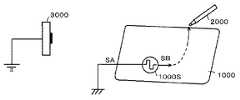
信号強度の低下が生じてしまう問題が生じる理由の一つは、アクティブスタイラスに静電結合により信号を送信する電子機器の信号処理回路のグランドが安定していないことに起因するものであり、これについて、図18〜図21を参照しながら説明する。 One of the reasons for the decrease in signal strength may be caused by the unstable ground of the signal processing circuit of the electronic device that transmits the signal to the active stylus by electrostatic coupling. Will be described with reference to FIGS.
図18及び図20に示すように、位置検出センサを備える電子機器1000の信号処理回路の信号送信回路1000Sから、アクティブスタイラス2000に対して信号が静電結合により送信される。この場合に、電子機器1000の電源として商用交流電源が用いられる場合と、内蔵バッテリーが用いられる場合とがあるが、内蔵バッテリーが用いられる場合には、電子機器の信号処理回路のグランドが安定しないという問題がある。 As shown in FIGS. 18 and 20, the
すなわち、電子機器1000の電源として商用交流電源が用いられる場合には、電子機器1000は、図18に示すように、ACアダプター3000に接続される。ACアダプター3000のグランドは、電位が安定している地球電位である外部グランドに接続されている。したがって、この場合には、電子機器1000の信号処理回路のグランド(以下、回路グランドという。)は、電子機器1000がACアダプター3000に接続されているので、外部グランドに結合される。 That is, when a commercial alternating current power supply is used as a power supply of the
このため、電子機器1000の信号送信回路1000Sの回路グランド(電子機器内のグランド電極に対応。以下同じ)側の点SAの電位は、外部グランドに結合されているので、図19(A)に示すように、安定している。このため、信号送信回路1000Sの出力端側の点SBの信号レベルは、図19(B)に示すように低下することはなく、位置検出センサからの送信信号の信号強度は低下することなくアクティブスタイラス2000に伝送される。 For this reason, the potential at the point SA on the circuit ground (corresponding to the ground electrode in the electronic device; the same applies hereinafter) of the
一方、図20に示すように、電子機器1000がACアダプター3000に接続されるのではなく、電子機器1000の電源として内蔵バッテリーが用いられる場合には、電子機器1000の信号処理回路の回路グランドは、外部グランドとは非結合となるので、浮いている状態となる。このため、外部グランドと電子機器1000の信号処理回路の回路グランドとの結合の大きさによっては、信号送信回路1000Sの回路グランド側の点SAの電位は、図21(A)に示すように、信号に応じて大きく振れてしまう。その結果、信号送信回路1000Sの出力端側の点SBの信号レベルは、図21(B)に示すように、ACアダプター3000に接続されている場合(図19(B)の場合)に比較して低下されてしまう。つまり、電子機器1000の位置検出センサからアクティブスタイラス2000に送信される信号の強度(振幅)が低下してしまう。 On the other hand, as shown in FIG. 20, when the
信号レベルの低下が生じてしまう理由の他の一つは、電子機器1000からの信号がアクティブスタイラス2000の使用者の人体を通じて回り込むことに起因するものであり、これについて、図22及び図23を参照しながら説明する。 Another reason for the reduction of the signal level is that the signal from the
アクティブスタイラス2000は、図22に示すように、電子機器1000の位置検出センサからの信号を、この例では、導体からなるアンテナ(図22の例では芯体)2001で受信し、その受信信号を例えばオペアンプ(演算増幅器)2002を通じ、また、周波数制限用のフィルタ2003を通じてコントローラ2004に供給する。コントローラ2004は、受信信号に応じて、図22では図示を省略した送信回路を制御するようにする。 As shown in FIG. 22, the
オペアンプ2002、フィルタ2003及びコントローラ2004には、内蔵バッテリー2005から電源電圧が供給される。そして、オペアンプ2002、フィルタ2003、コントローラ2004及び内蔵バッテリー2005は、アクティブスタイラス2000の回路グランドに接続されている。このアクティブスタイラス2000の回路グランドは導電性を有する筐体にも接続されており、受信信号を増幅するオペアンプ2002の基準電位となる。 A power supply voltage is supplied to the operational amplifier 2002, the filter 2003 and the controller 2004 from the built-in battery 2005. The operational amplifier 2002, the filter 2003, the controller 2004 and the built-in battery 2005 are connected to the circuit ground of the
この場合、電子機器1000とアンテナ2001との間は結合容量Ctを介して静電結合される。また、アクティブスタイラス2000が使用者により把持されて電子機器1000の位置検出センサ上で使用される状態では、アクティブスタイラス2000の回路グランドと電子機器1000の位置検出センサとの間で、容量Ch及び抵抗Rhで等価される人体を介して静電結合される状態になる。 In this case, the
そして、電子機器1000とアンテナ2001との間の結合容量Ctと、電子機器1000とアクティブスタイラス2000の回路グランドとの間の結合容量Chとの差が小さい場合には、電子機器1000からの信号が人体を通じてアクティブスタイラス2000に回り込むようになる。オペアンプ2002は、アクティブスタイラス2000の回路グランドとアンテナ2001との間の差動信号を検出しており、この電子機器1000から回り込む信号のため、アクティブスタイラス2000の受信信号の信号強度が小さくなってしまう。場合によっては、電子機器1000からの信号の波形の位相が、アクティブスタイラス2000内部で反転してしまう場合もある。 When the difference between the coupling capacitance Ct between the
図23に、結合容量Ctとアンテナ2001との結合点PA(図23(A)参照)と、アクティブスタイラス2000の回路グランドと結合容量Chとの結合点PB(図23(B))と、オペアンプ2002の出力端PC(図23(C)参照)との、それぞれにおける信号強度の例を示す。この図23に示すように、オペアンプ2002の出力端PC(図23(C)参照)の信号強度は、結合容量Ctと結合容量Chとの大小関係に応じて小さくなったり、反転してしまったりする。 23, a coupling point PA of the coupling capacitance Ct and the antenna 2001 (see FIG. 23A), a coupling point PB of the circuit ground of the
すなわち、結合容量Ctが結合容量Chよりも大きい(Ct>Ch)ときには、図23(A),(B),(C)において、左側に示すようになり、オペアンプ2002の出力端PCの信号強度は、小さくなる。また、結合容量Ctが結合容量Chと等しい(Ct=Ch)ときには、図23(A),(B),(C)において、中央に示すようになり、オペアンプ2002の出力端PCの信号強度はゼロになる。さらに、結合容量Ctが結合容量Chよりも小さい(Ct<Ch)ときには、図23(A),(B),(C)において、右側に示すようになり、オペアンプ2002の出力端PCの信号強度は小さくなると共に、信号が反転した状態となってしまう。 That is, when the coupling capacitance Ct is larger than the coupling capacitance Ch (Ct> Ch), as shown on the left side in FIGS. 23A, 23B, and 23C, the signal strength of the output end PC of the operational amplifier 2002 is obtained. Becomes smaller. In addition, when the coupling capacitance Ct is equal to the coupling capacitance Ch (Ct = Ch), as shown in the center in FIGS. 23A, 23 B, and 23 C, the signal strength of the output end PC of the operational amplifier 2002 is It becomes zero. Further, when the coupling capacitance Ct is smaller than the coupling capacitance Ch (Ct <Ch), as shown in the right side in FIGS. 23A, 23 B, and 23 C, the signal strength of the output end PC of the operational amplifier 2002 is obtained. Becomes smaller and the signal becomes inverted.
なお、図22に示した例では、アクティブスタイラス2000では筐体が導体で構成され、当該筐体が回路グランドとなるようにされているように示したが、筐体が導体で構成される必要はない。すなわち、アクティブスタイラス2000内のプリント基板にグランド導体が形成されている場合においても、使用者の人体とプリント基板のグランド導体とが容量結合されることで、上述と同様の問題が生じる。 In the example shown in FIG. 22, the case is made of a conductor in the
この発明は、以上の問題点を解決することを目的とする。 An object of the present invention is to solve the above problems.
上記の課題を解決するために、この発明は、
位置検出領域に対応して配置された複数の導体を有し、使用者が把持するアクティブスタイラスが指示する位置と、前記アクティブスタイラスを把持する前記使用者の手によるタッチが検出可能なタッチパネルであって、
前記タッチパネルとの間での静電結合を介して前記タッチパネルから送信される信号が受信可能に構成された前記アクティブスタイラスに対し、前記静電結合を介して信号を送信する信号送信回路と、
前記アクティブスタイラスとの間での静電結合を介して前記アクティブスタイラスが指示する位置を検出するアクティブスタイラス指示位置検出回路と、
前記使用者の手がタッチされたことを検出するタッチ検出回路と、
前記タッチ検出回路によるタッチ検出結果に対応して、前記タッチパネルに配置された導体であって前記タッチ検出回路でタッチが検出された前記使用者の手と静電結合している導体を前記タッチパネルのグランドへカップリングさせるカップリング制御を行うカップリング制御回路と
を備えていることを特徴とするタッチパネルを提供する。In order to solve the above problems, the present invention is
A touch panel having a plurality of conductors arranged corresponding to a position detection area, and capable of detecting a position indicated by an active stylus gripped by a user and a touch by the user's hand gripping the active stylus. ,
A signal transmission circuit for transmitting a signal via the electrostatic coupling to the active stylus configured to be capable of receiving a signal transmitted from the touch panel via the electrostatic coupling between the touch panel and the touch panel;
An active stylus pointing position detection circuit that detects a position indicated by the active stylus through capacitive coupling with the active stylus;
A touch detection circuit that detects that the user's hand has been touched;
The conductor disposed on the touch panel corresponding to the touch detection result by the touch detection circuit, the conductor electrostatically coupled to the user's hand whose touch is detected by the touch detection circuit And a coupling control circuit for performing coupling control to be coupled to the ground.
上述の構成の発明によるタッチパネルにおいては、使用者がアクティブスタイラスを把持してタッチパネルの上に持ち来すと、使用者の手がタッチパネルにタッチされたことが検出され、そのタッチが検出された使用者の手と静電結合している導体が、タッチパネルのグランド(回路グランド)にカップリングされる。すると、タッチパネルのグランド(回路グランド)にカップリングされた導体は、使用者の人体を通じて外部グランドにカップリングされる。 In the touch panel according to the invention of the above-mentioned configuration, when the user holds the active stylus and brings it on the touch panel, it is detected that the user's hand is touched on the touch panel and the touch is detected. A conductor that is capacitively coupled to the person's hand is coupled to the touch panel ground (circuit ground). Then, the conductor coupled to the touch panel ground (circuit ground) is coupled to the external ground through the user's human body.
このため、タッチパネルのグランド(回路グランド)が外部グランドに接続されていないときにも、タッチパネルのグランド(回路グランド)がタッチパネルにタッチしている人体(手)を通じて外部グランドに接続される状態となり、アクティブスタイラスに送信される信号の強度は低下しない。 Therefore, even when the touch panel ground (circuit ground) is not connected to the external ground, the touch panel ground (circuit ground) is connected to the external ground through the human body (hand) touching the touch panel. The strength of the signal sent to the active stylus is not reduced.
また、タッチパネルのグランド(回路グランド)が外部グランドに接続されることで、外部グランドに接続されている人体の手と強く結合されることになる。したがって、アクティブスタイラスを把持している人体の手を通じてアクティブスタイラスに回り込むタッチパネルからの信号を外部グランドに流すことで、抑制することができる。このため、アクティブスタイラスで受信された信号の強度が低下したり、反転したものされてしまうのを軽減あるいは防止することができる。 Further, by connecting the ground (circuit ground) of the touch panel to the external ground, the touch panel is strongly coupled to the human hand connected to the external ground. Therefore, it is possible to suppress the signal from the touch panel, which flows around the active stylus through the hand of the human body holding the active stylus, to the external ground. For this reason, it is possible to reduce or prevent that the strength of the signal received by the active stylus is reduced or inverted.
この発明によれば、タッチパネルのグランド(回路グランド)が外部グランドに接続されていないときにも、タッチパネルのグランド(回路グランド)がタッチパネルにタッチしている人体(手)を通じて外部グランドに接続される状態となり、アクティブスタイラスに送信される信号の強度の低下を軽減あるいは防止することができる。 According to the present invention, even when the touch panel ground (circuit ground) is not connected to the external ground, the touch panel ground (circuit ground) is connected to the external ground through the human body (hand) touching the touch panel In this state, it is possible to reduce or prevent the reduction in the strength of the signal transmitted to the active stylus.
また、タッチパネルのグランド(回路グランド)が外部グランドに接続されることで、外部グランドに接続されている人体の手と強く結合されることになるので、人体の手を通じてアクティブスタイラスに回り込むタッチパネルからの信号を外部グランドに流すことで抑制することができ、アクティブスタイラスで受信された信号の強度が低下したり、反転したものされてしまうのを軽減あるいは防止することができる。 In addition, since the touch panel ground (circuit ground) is connected to the external ground, it is strongly coupled to the human hand connected to the external ground, and therefore, the touch panel from the touch panel can move around the active stylus through the human hand. A signal can be suppressed by passing the signal to an external ground, and reduction or reduction in the strength of the signal received by the active stylus or reduction thereof can be reduced or prevented.
以下、この発明によるタッチパネルの実施形態を、図を参照しながら説明する。なお、以下に説明するタッチパネルの実施形態は、この発明による信号処理装置及び回路グランドと外部グラントとのカップリング方法の実施形態を含むものである。この場合の外部グランドとしては、通常は地球電位とされるが、安定な固定電位であれば地球電位に限られるものではない。 Hereinafter, an embodiment of a touch panel according to the present invention will be described with reference to the drawings. The embodiment of the touch panel described below includes the embodiments of the signal processing device and the method of coupling the circuit ground and the external grant according to the present invention. The external ground in this case is usually the earth potential, but is not limited to the earth potential as long as it is a stable fixed potential.
図1は、この発明の信号処理装置及び回路グランドと外部グラントとのカップリング方法の一実施形態が適用されて構成された、この実施形態のタッチパネル1を備えた電子機器2の一例を示すものである。図1に示す例の電子機器2は、例えばLCD(Liquid Crystal Display)などの表示装置の表示画面2Dを備える、例えばパッド型パソコンやスマートフォンと呼ばれる携帯電話端末などの携帯機器であり、表示画面2Dの前面部にはタッチパネル1を構成するセンサ(位置検出センサ)10が配設されている。そして、この電子機器2は、この例では電源としてバッテリー(図示は省略)を用いるものとされている。 FIG. 1 shows an example of an
電子機器2の表示画面2Dの前面部に配設されたセンサ10上で指示体により位置指示操作が行われると、タッチパネル1は、指示体により指示された位置を検出し、電子機器2が備えるマイクロコンピュータによって操作位置に応じた表示処理を施すことができる。この例においては、タッチパネル1は、指示体として、使用者の手や指3と、送信信号を送出するアクティブ静電ペンであるアクティブスタイラス4との両方を検出することできるように構成されている。 When a position indicating operation is performed by the pointer on the
[タッチパネル1の構成例]
次に、この実施形態のタッチパネル1の構成例について説明する。図2は、この実施形態のタッチパネル1の概略構成例を説明するための図である。この例のタッチパネル1は、いわゆるクロスポイント構成のセンサ10を備えており、手や指3などの指示体による静電タッチ(以下、単にタッチという)を検出することができると共に、アクティブスタイラス4により指示された位置(以下、ペン指示位置という)を検出することができるように構成されている。[Configuration Example of Touch Panel 1]
Next, a configuration example of the
センサ10は、この例では、下層側から順に、第1の導体群11、絶縁層(図示は省略)、第2の導体群12を積層して形成されたものである。第1の導体群11は、第1の方向、例えば、横方向(X軸方向)に延在した第1の導体11Y1、11Y2、…、11Ym(mは1以上の整数)を互いに所定間隔離して並列に配置されている
また、第2の導体群12は、この例では、第1の導体11Y1、11Y2、…、11Ymの延在方向に対して交差するY軸方向に延在した第2の導体12X1、12X2、…、12Xn(nは1以上の整数)を互いに所定間隔離して並列に配置されている。In this example, the
なお、以下の説明において、第1の導体11Y1、11Y2、…、11Ymについて、それぞれの導体を区別する必要がないときには、その導体を、第1の導体11Yと称する。同様に、第2の導体12X1、12X2、…、12Xnについて、それぞれの導体を区別する必要がないときには、その導体を、第2の導体12Xと称することとする。In the following description, when it is not necessary to distinguish between the
このように、タッチパネル1では、第1の導体群11と第2の導体群12を交差させて形成したセンサパターンにより規定される位置検出領域において、手や指3やアクティブスタイラス4などの指示体が指示する位置を検出する構成を備えている。 As described above, in the
この実施形態のタッチパネル1のセンサ10の位置検出領域は、電子機器2が備える表示装置の表示画面2Dの画面サイズに対応し、画面サイズと同等の大きさの指示入力面10Sを備えており、光透過性を有する、第1の導体群11と第2の導体群12とによって形成されている。 The position detection area of the
この実施形態のタッチパネル1のセンサ10において、手や指3のタッチを検出する場合は、第1の方向に配置された第1の導体群11に送信信号を供給すると共に、第2の方向に配置された第2の導体群12から信号を受信するように構成されている。また、アクティブスタイラス4による指示位置を検出する場合には、第1の導体群11及び第2の導体群12のそれぞれからの信号を受信する構成となる。なお、クロスポイント型静電容量方式の位置検出装置の原理等については、この出願の発明者の発明に係る出願の公開公報である特開2011−3035号公報、特開2011−3036号公報、特開2012−123599号公報等に詳しく説明されている。 In the
この実施形態のタッチパネル1は、図2に示すように、タッチパネル(位置検出センサ)を構成するセンサ10と、このセンサ10に接続される信号処理回路20とで構成されている。信号処理回路20は、センサ10との入出力インターフェースとされるYマルチプレクサ21Y及びXマルチプレクサ21Xと、コマンド生成回路22と、タッチ検出用信号生成回路23と、タッチ検出回路24と、ペン指示検出回路25と、Yグランドセレクタ26Y及びXグランドセレクタ26Xと、制御回路27とからなる。 As shown in FIG. 2, the
Yマルチプレクサ21Yは、第1の導体群11と、コマンド生成回路22、タッチ検出用信号生成回路23及びペン指示検出回路25との間に設けられており、制御回路27の制御により、第1の導体群11を構成する複数の第1の導体11Yのそれぞれと、コマンド生成回路22、タッチ検出用信号生成回路23及びペン指示検出回路25との接続が切り替えられる。 The
Xマルチプレクサ12Xは、第2の導体群12と、タッチ検出回路24及びペン指示検出回路25との間に設けられており、制御回路27の制御により、第2の導体群12を構成する複数の第2の導体12Xのそれぞれと、タッチ検出回路24及びペン指示検出回路25との接続が切り替えられる。 The
コマンド生成回路22は、第1の導体群11を通じてアクティブスタイラス4に送信するコマンド信号を生成し、Yマルチプレクサ21Yに供給する。コマンド信号としては、アクティブスタイラス4に対して、当該アクティブスタイラス4が使用する周波数を設定する設定コマンドや、アクティブスタイラス4における位置検出用信号や筆圧検出信号の送出タイミングを指示するコマンドなどを含む。そして、コマンド生成回路22は、制御回路27からの制御信号を受けて、その制御信号に応じたコマンド信号を生成し、送出する。この例では、コマンド生成回路22からのコマンド信号は、Yマルチプレクサ21Yを通じて第1の導体群11の複数の第1の導体11Yに供給される。 The
タッチ検出用信号生成回路23は、制御回路27からの制御信号に基づいてタッチ検出用信号を生成し、Yマルチプレクサ21Yに供給する。タッチ検出用信号としては、この例では、例えばアダマール行列などの直交行列からなる拡散符号が用いられ、Yマルチプレクサ21Yを通じて第1の導体群11の複数の第1の導体11Yに供給される。 The touch detection signal generation circuit 23 generates a touch detection signal based on the control signal from the
タッチ検出回路24は、センサ10における手や指3の位置を検出する機能を有する。すなわち、複数個の第1の導体11Yと複数個の第2の導体12Xとを交差させて形成したセンサパターンのそれぞれの交点(クロスポイント)における第1の導体11Yと第2の導体12Xとの間の静電容量が、手や指3によりタッチ指示された位置では変化するので、その静電容量の変化を検出することにより、センサ10上のタッチの位置を検出するようにする。 The
この実施形態では、タッチ検出用信号生成回路23からの送信信号(この例では拡散符号)を第1の導体群11Yに供給し、第1の導体11Yと第2の導体12Xとの間の静電容量(相互容量)を介して第2の導体12Xから受信信号を得る。タッチ検出回路24は、手や指3がタッチされたクロスポイント位置では、人体を通じて外部グランドに接続されるために静電容量(相互容量)が変化することに基づいて、その位置の第2の導体12Xからの受信信号のレベル(拡散符号の相関レべル)が変化することを検知することで、タッチ位置を検出する。タッチ検出回路24には、受信信号から拡散符号の相関レべルを検出するために、タッチ検出用信号生成回路23から第1の導体群11Yに供給される送信信号(拡散符号)に対応した信号(相関演算用拡散符号)が供給されている。そして、タッチ検出回路24は、検出したタッチ位置の検出結果を制御回路27に供給する。 In this embodiment, a transmission signal (a diffusion code in this example) from the touch detection signal generation circuit 23 is supplied to the
ペン指示検出回路25は、センサ10上におけるアクティブスタイラス4による指示位置を検出するものである。アクティブスタイラス4は、後述するように、内部に発信回路4S(図1参照)を備え、この発信回路4Sからの信号をペン先の電極から送出する。なお、発信回路4Sは、発振器で構成してもよいし、発振器で発生した発振信号に変調などの処理を施した信号を発生する回路であってもよい。ペン指示検出回路25は、このアクティブスタイラス4からの信号を、センサ10の第2の導体群12からのみならず、第1の導体群11からも受信する。なお、この例のアクティブスタイラス4は、ペン先の電極をアンテナとしてタッチパネル1からの送信信号を受信する。 The pen pointing
ペン指示検出回路25は、第1の導体群11及び第2の導体群12を構成するそれぞれの第1の導体11Y及び第2の導体12Xについて、アクティブスタイラス4からの信号の受信信号のレベルをチェックして、当該受信信号が高レベルとなっている第1の導体11Y及び第2の導体12Xを検出して、アクティブスタイラス4が指示する位置を検出するようにする。そして、ペン指示検出回路25は、アクティブスタイラス4が指示する位置についての検出結果を制御回路27に供給する。 The pen pointing
Yグランドセレクタ26Yは、この例では、第1の導体群11と、Yマルチプレクサ21Yとの間に設けられ、第1の導体群11の第1の導体11Yのそれぞれと、タッチパネル1の回路グランドとのカップリングを、制御回路27の制御により制御する。 In this example, the
ここで、導体と回路グランドとのカップリングとは、導体のそれぞれと回路グランドとが直接的に接続される場合に限らず、導体と回路グランドとが抵抗や容量を介して接続されている場合を含むものである。 Here, the coupling between the conductor and the circuit ground is not limited to the case where each of the conductors and the circuit ground are directly connected, but the case where the conductor and the circuit ground are connected via a resistor or a capacitor. Is included.
図3は、このYグランドセレクタ26Yの構成例を示すものである。すなわち、第1の導体群11を構成する第1の導体11Y1、…、11Ym−1、11Ymのそれぞれは、Yマルチプレクサ21Yに接続されると共に、スイッチ回路26Y1、…、26Ym−1、26Ymのそれぞれを通じて、タッチパネル1の回路グランドSGに、この例では直接に接続される。そして、スイッチ回路26Y1、…、26Ym−1、26Ymのそれぞれのオン、オフが制御回路27からの制御信号により切り替え制御される。FIG. 3 shows a configuration example of the
図4は、Xグランドセレクタ26Xの構成例を示すものである。Xグランドセレクタ26Xは、この例では、第2の導体群12と、Xマルチプレクサ21Xとの間に設けられ、第2の導体群12の第2の導体12Xのそれぞれと、タッチパネル1の回路グランドSGとのカップリングを、制御回路27の制御により制御する。すなわち、第2の導体群12を構成する第2の導体12X1、12X2、…、12Xnのそれぞれは、Xマルチプレクサ21Xに接続されると共に、スイッチ回路26X1、26X2、…、26Xnのそれぞれを通じて、タッチパネル1の回路グランドSGに、この例では直接に接続される。そして、スイッチ回路26X1、26X2、…、26Xnのそれぞれのオン、オフが制御回路27からの制御信号により切り替え制御される。FIG. 4 shows a configuration example of the
制御回路27は、タッチパネル1の全体の動作を制御するためのもので、この例では、MPU(microprocessor unit)で構成されており、導体と回路グランドとのカップリングを制御するカップリング制御回路の機能を備えている。 The
この実施形態のタッチパネル1は、アクティブスタイラス4に対するアップリンク(送信)とダウンリンク(受信)とを時分割で行うと共に、手や指3のタッチ検出とアクティブスタイラス4による指示位置の検出とを時分割で行うように制御するように構成されている。制御回路27は、この時分割処理を管理する。 The
すなわち、この実施形態のタッチパネル1では、図5に示すように、アップリンクの期間とダウンリンクの期間とを時分割で交互に実行するようにする。そして、アップリンクの期間は、コマンド生成回路22からのコマンド信号をアクティブスタイラス4に対して送信するコマンド送信期間である。また、ダウンリンクの期間は、位置検出期間として、その前半は、手や指3によるタッチパネル1へのタッチを検出するタッチ検出期間であり、その後半は、アクティブスタイラス4による指示位置を検出するペン指示検出期間である。 That is, in the
制御回路27は、アップリンク期間のコマンド送信期間では、Yマルチプレクサ21Yを、コマンド生成回路22からのコマンド信号をYグランドセレクタ26Yを通じて第1の導体群11の複数の導体11Yのそれぞれに供給する状態になるように制御する。このとき、制御回路27は、タッチ検出回路24及びペン指示検出回路25が非動作状態となるように制御する。 The
また、制御回路27は、ダウンリンク期間の位置検出期間の前半のタッチ検出期間では、Yマルチプレクサ21Yをタッチ検出用信号生成回路23からのタッチ検出用信号(この例では拡散符号)を、Yグランドセレクタ26Yを通じて第1の導体群11の第1の導体11Yのそれぞれに供給する状態になるように制御する。そして、このタッチ検出期間では、制御回路27は、Xマルチプレクサ21Xを、第2の導体群12の複数の第2の導体12Xのそれぞれに得られる受信信号をタッチ検出回路24に供給する状態となるように制御する。このとき、制御回路27は、コマンド生成回路22及びペン指示検出回路25が非動作状態になるように制御する。 Further, in the touch detection period in the first half of the position detection period of the downlink period, the
このタッチ検出期間においては、タッチ検出用信号生成回路23からのタッチ検出用信号(この例では拡散符号)が、第1の導体群11の複数の第1の導体11Yから第2の導体群12の複数の第2の導体12Xに、それら間の静電結合を通じて伝送される。 During the touch detection period, the touch detection signal (a diffusion code in this example) from the touch detection signal generation circuit 23 is transmitted from the plurality of
タッチ検出回路24では、Xマルチプレクサ21Xから出力される第2の導体群12の複数の第2の導体12Xのそれぞれに得られる前記タッチ検出用信号(この例では拡散符号)の受信信号と、タッチ検出用信号生成回路23からの位置検出用信号(この例では相関演算用拡散符号)との相関を演算することにより、手や指3がタッチされていて、送信信号であるタッチ検出用信号が低下しているクロスポイントを検出することで、手や指3のタッチ位置を検出する。 In the
なお、このタッチ検出期間では、タッチ検出用信号によるタッチ検出を1回のみ行うようにしてもよいし、複数回繰り返して行うようにしてもよい。 In the touch detection period, touch detection using a touch detection signal may be performed only once, or may be repeatedly performed a plurality of times.
また、制御回路27は、ダウンリンク期間の位置検出期間の後半のペン指示検出期間では、第1の導体群11の第1の導体11Yのそれぞれに得られる信号がペン指示検出回路25に供給される状態になるようにYマルチプレクサ21Yを制御すると共に、Xマルチプレクサ21Xを、第2の導体群12の複数の第2の導体12Xのそれぞれに得られる受信信号がペン指示検出回路25に供給される状態になるように制御する。このとき、制御回路27は、コマンド生成回路22、タッチ検出用信号生成回路23及びタッチ検出回路24が非動作状態になるように制御する。 Further, in the pen indication detection period in the second half of the position detection period of the downlink period, the
このペン指示検出期間においては、アクティブスタイラス4から送信される位置検出用信号を、第1の導体群11及び第2の導体群12のそれぞれにおいて検出するようにする。すなわち、ペン指示検出回路25では、先ず、Yマルチプレクサ21Yから出力される第1の導体群11の複数の第1の導体11Yのそれぞれに得られる、アクティブスタイラス4からの受信信号のレベルを検出し、その受信レべルが所定値より大になっている複数の第1の導体11Yを検出し、それらの複数の第1の導体11Yからアクティブスタイラス4により指示されているセンサ10上のY方向位置を検出する。 In this pen pointing detection period, the position detection signal transmitted from the active stylus 4 is detected in each of the first conductor group 11 and the second conductor group 12. That is, in the pen pointing
また、ペン指示検出回路25は、Xマルチプレクサ21Xから出力される第2の導体群12の複数の第2の導体12Xのそれぞれに得られる、アクティブスタイラス4からの位置検出用信号の受信信号のレベルを検出し、その受信レべルが所定値より大になっている複数の第2の導体12Xを検出し、それらの複数の第2の導体12Xからアクティブスタイラス4により指示されているセンサ10上のX方向位置を検出する。 In addition, the pen pointing
そして、ペン指示検出回路25は、検出したY方向位置とX方向位置とから、アクティブスタイラス4により指示されているセンサ10上の座標位置を検出する。 Then, the pen
そして、この実施形態では、制御回路27は、タッチ検出期間で、タッチパネル1における手や指3のタッチを検出したときには、その後のコマンド送信期間において、そのタッチ位置に含まれる第1の導体11Y及び/又は第2の導体12Xの内の、少なくとも1本の導体を回路グランドSGにカップリングさせるように、Yグランドセレクタ26Yのスイッチ回路26Y1〜26Ym、Xグランドセレクタ26Xのスイッチ回路26X1〜26Xnを切り替え制御するようにする。Then, in this embodiment, when the
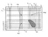
すなわち、使用者がアクティブスタイラス4を把持して、例えば図6に示すように、センサ10の入力面10S上において、アクティブスタイラス4により位置指示する場合、使用者の手3Hの掌の一部が入力面10Sにタッチする状態となることが多い。タッチパネル1のタッチ検出回路24は、タッチ検出期間において、この使用者の手3Hの掌の一部のタッチ位置を、センサ10上において、例えば図7において斜線を付して示した領域AHとして検出し、当該タッチ検出結果の情報を制御回路27に通知する。 That is, when the user holds the active stylus 4 and designates the position by the active stylus 4 on the input surface 10S of the
制御回路27は、このタッチ検出回路24からのタッチ検出結果の情報に基づいて、その後のコマンド送信期間において、領域AH内の、センサ10の入力面10Sに、より強くタッチしていると思われる例えば領域AHの中央位置の第1の導体11Y4及び第2の導体12Xn−7を、回路グランドSGにカップリングするように、Yグランドセレクタ26Y及び/又はXグランドセレクタ26Xを制御する。すなわち、制御回路27は、この例では、検出されたタッチ位置の領域を判定し、その判定したタッチ位置の領域に基づいて、使用者の手や指と静電結合していて、人体を通じてより強く外部グランドにカップリングすることが可能な導体を特定し、その特定された導体を回路グランドSGにカップリングするように制御する。The
このように、タッチ検出期間において検出された、タッチパネル1における手や指3のタッチ位置に対応した所定数の導体は、その後のコマンド送信期間においては、回路グランドSGにカップリングされるので、図8に示すように、タッチパネル1の回路グランド側は、抵抗Rh及び容量Chで等価される人体5を通じて外部グランドEGにカップリングされる。したがって、タッチパネル1からアップリンクのコマンド送信期間でアクティブスタイラス4に送信されるコマンド信号の信号強度は低下することなく送信できる。 As described above, a predetermined number of conductors corresponding to the touch position of the hand or
そして、タッチパネル1の回路グランドSGが外部グランドEGにカップリングされることで、外部グランドにカップリングされている人体5と強く結合されることになるので、人体の手を通じてアクティブスタイラス4に回り込むタッチパネルからの信号を外部グランドEGに流すことができ、アクティブスタイラス4で受信されたコマンド信号の強度が低下したり、反転したものされてしまうのを軽減あるいは防止することができる。 Then, since the circuit ground SG of the
なお、上述の例では、コマンド送信期間において、そのタッチ位置に含まれる第1の導体11Y及び/又は第2の導体12Xの内のそれぞれ1本ずつを回路グランドSGにカップリングした。しかし、カップリングする導体数は、これに限られるものではなく、検出したタッチ位置に含まれる第1の導体11Y及び第2の導体12Xの内の、全部の導体を回路グランドとカップリングさせるようにしてもよいし、一部の複数本の導体を回路グランドとカップリングさせるようにしてもよい。一部の複数本の導体を回路グランドとカップリングする場合にも、制御回路27は、上述と同様にして、検出したタッチ領域のパターンに基づいて、回路グランドSGとカップリングさせる複数の導体を特定するようにする。 In the above example, in the command transmission period, one each of the
また、第1の導体11Yは、コマンド送信期間には、コマンド信号の送信用として用いられるが、回路グランドSGにカップリングされた第1の導体11Yは、送信信号を外部に送出することができず、コマンド信号の送信には用いられなくなる。そこで、第1の導体群11の複数の第1の導体11Yは、回路グランドSGへのカップリング用としては用いず、第2の導体群12の複数の第2の導体12Xのみを、回路グランドSGへのカップリング用として用いるように構成してもよい。 In addition, although the
[タッチパネル1の制御回路27の動作の流れの例]
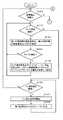
この実施形態のタッチパネル1の制御回路27の動作の流れの例を、図9及び図10のフローチャートを参照しながら以下に説明する。[Example of Flow of Operation of
An example of the flow of the operation of the
制御回路27は、位置検出期間であるか否か判別し(ステップS101)、位置検出期間であると判別したときには、タッチ検出期間であるか否か判別する(ステップS102)。このステップS102で、タッチ検出期間であると判別したときには、制御回路27は、前述したようにして、第1の導体群11の複数の第1の導体11Yに、タッチ検出用信号生成回路23からのタッチ検出用信号を供給すると共に、第2の導体群12の複数の第1の導体12Xのそれぞれからタッチ検出用信号の受信信号を受信して、両者の相関を演算することにより、手や指3のタッチを検出するように制御する(ステップS103)。 The
そして、制御回路27は、ステップS103でのタッチ検出の結果、手や指のタッチを検出したか否か判別し(ステップS104)、手や指3のタッチを検出しなかったと判別したときには、処理をステップS102に戻し、このステップS102以降の処理を繰り返す。 Then, as a result of the touch detection in step S103, the
また、ステップS104で、手や指3のタッチを検出したと判別したときには、制御回路27は、センサ10上のタッチ位置(タッチ領域)を検出して、それを電子機器のホストコンピューターに伝送すると共に、当該タッチ位置の第1の導体11Y及び/または第2の導体12Xの1本あるいは複数本、または全部を、コマンド送信期間に回路グランドSGにカップリングする導体として決定し、それをバッファメモリに記憶する(ステップS105)。このステップS105の次には、制御回路27は、処理をステップS102に戻し、このステップS102以降の処理を繰り返す。 When it is determined in step S104 that the touch of the hand or
そして、ステップS102で、タッチ検出期間ではない(あるいはタッチ検出期間が終了した)と判別したときには、制御回路27は、ペン指示検出期間であるか否か判別する(ステップS106)。このステップS106でペン指示検出期間であると判別したときには、制御回路27は、前述したように、第1の導体11Y及び第2の導体12Xの全てを受信導体として、アクティブスタイラス4からの位置検出用信号を受信することに基づいて、アクティブスタイラス4によって指示されたセンサ10上の位置を検出するように制御する(ステップS107)。 When it is determined in step S102 that the touch detection period is not in progress (or the touch detection period has ended), the
そして、制御回路27は、センサ10上のペン指示位置の検出結果を電子機器のホストコンピューターに伝送する(ステップS108)。このステップS108の次には、制御回路27は、処理をステップS106に戻し、このステップS106以降の処理を繰り返す。そして、ステップS106で、ペン指示検出期間ではない(あるいはペン指示検出期間が終了した)と判別したときには、制御回路27は、処理をステップS101に戻し、このステップS101以降の処理を繰り返す。 Then, the
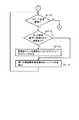
ステップS101で、位置検出期間ではない(あるいは位置検出期間は終了した)と判別したときには、制御回路27は、コマンド送信期間であるか否か判別する(図10のステップS111)。ステップS111で、コマンド送信期間ではない(あるいはコマンド送信期間は終了した)と判別したときには、制御回路27は、処理をステップS101に戻し、このステップS101以降の処理を繰り返す。 When it is determined in step S101 that the position detection period is not (or the position detection period has ended), the
ステップS111で、コマンド送信期間であると判別したときには、制御回路27は、タッチ検出期間において回路グランドSGにカップリングする導体が記憶されているか否か判別する(ステップS112)。このステップS112で、回路グランドSGにカップリングされる導体が記憶されていると判別したときには、制御回路27は、当該記憶されている導体を、回路グランドSGにカップリングするように、Yグランドセレクタ26Y及び/またはXグランドセレクタ26Xを制御するようにする(ステップS113)。 When it is determined in step S111 that it is a command transmission period, the
そして、制御回路27は、第1の導体群11の複数の導体11Yからコマンド信号を送信させるように制御する(ステップS114)。ステップS112で、回路グランドSGにカップリングする導体が記憶されていないと判別したときには、制御回路27は、ステップS114に進み、第1の導体群11の複数の導体11Yからコマンド信号を送信させるように制御する。 Then, the
そして、制御回路27は、このステップS114の次には、ステップS111に戻り、このステップS111以降の処理を繰り返す。 Then, after the step S114, the
[上述の実施形態の変形例]
上述の実施形態では、タッチパネル1において、アクティブスタイラス4へのコマンド送信処理と、タッチ検出処理と、ペン指示検出処理とを時分割処理とするようにしたが、時分割処理に限らず、それぞれの処理において使用する周波数を異ならせることによる周波数多重処理や拡散符号を用いた多重処理として、同時並行的な処理とするようにしてもよい。また、必要に応じて時分割処理と周波数多重処理や拡散符号を用いた多重処理とを併用するようにしてもよい。[Modification of the above-mentioned embodiment]
In the above-described embodiment, in the
この場合、例えば周波数多重処理による同時並行的な処理を考慮する場合には、図11に示すように、周波数の異なる複数の信号を使用することができる。例えば、コマンド信号には、周波数f1を割り当て、タッチ検出用信号には、周波数f2(≠f1)を割り当て、ペン指示検出用信号には、周波数f3(≠f1≠f2)を割り当てるようにする。 In this case, in consideration of, for example, concurrent processing by frequency multiplexing processing, as shown in FIG. 11, a plurality of signals with different frequencies can be used. For example, the frequency f1 is assigned to the command signal, the frequency f2 (≠ f1) is assigned to the touch detection signal, and the frequency f3 (≠ f1 ≠ f2) is assigned to the pen instruction detection signal.
そして、アクティブスタイラス4の受信回路のオペアンプの出力信号に対しては、周波数f1を中心とした帯域成分を抽出するためのバンドパスフィルタを設ける。また、タッチパネル1のタッチ検出回路24の受信信号の入力側には、周波数f2を中心とした帯域成分を抽出するためのバンドパスフィルタを設け、また、ペン指示検出回路25の受信信号の入力側には、周波数f3を中心とした帯域成分を抽出するためのバンドパスフィルタを設ける。 Then, for the output signal of the operational amplifier of the reception circuit of the active stylus 4, a band pass filter for extracting a band component centered on the frequency f1 is provided. Further, on the input side of the reception signal of
このように周波数多重や拡散符号を用いた多重処理によりコマンド信号送信処理と、ペン指示検出処理とを同時並行的に実行する場合には、コマンド信号の送信処理と、アクティブスタイラス4により指示された位置の検出の処理とが並行して行われることになるので、回路グランドSGにカップリングさせる導体の選定に当たっては、ペン指示検出処理に、できるだけ影響を与えないように考慮する必要がある。 As described above, when command signal transmission processing and pen indication detection processing are simultaneously performed in parallel by multiplexing processing using frequency multiplexing or spreading code, the command signal transmission processing and the instruction from the active stylus 4 are used. Since the position detection process is performed in parallel, in selecting a conductor to be coupled to the circuit ground SG, it is necessary to consider the pen indication detection process as little as possible.
すなわち、タッチ検出処理により、例えば図7に示したように手の掌のタッチ領域AHが検出されたときに、例えばペン指示検出処理で検出されるペン指示位置が、図7における位置PSであるときには、当該位置PSの位置の近傍の第1の導体11Y及び第2の導体12Xは、領域AHを通る第1の導体11Y及び第2の導体12Xとは異なる。したがって、この場合には、領域AHを通る第1の導体11Y及び第2の導体12Xのいずれを、回路グランドにカップリングさせても、ペン指示検出に影響はない。 That is, for example, when the touch area AH of the palm of the hand is detected as shown in FIG. 7 by the touch detection process, for example, the pen pointing position detected by the pen pointing detection process is the position PS in FIG. Sometimes, the
しかし、例えばペン指示検出処理で検出されるペン指示位置が、図7における位置PS1であるときには、当該位置PS1の位置の近傍の第1の導体11Yが領域AHを通っているため、この第1の導体11Yを回路グランドSGにカップリングさせてしまうと、ペン指示位置の検出が困難になる。そこで、この場合には、領域AHを通る第1の導体11Yは回路グランドSGにカップリングさせることなく、領域AHを通る第2の導体12Xを回路グランドSGにカップリングさせるようにする。 However, for example, when the pen pointing position detected in the pen pointing detection process is the position PS1 in FIG. 7, the
また、例えばペン指示検出処理で検出されるペン指示位置が、図7における位置PS2であるときには、当該位置PS2の位置の近傍の第2の導体12Xが領域AHを通っているため、この第2の導体12Xを回路グランドSGにカップリングさせてしまうと、ペン指示位置の検出が困難になる。そこで、この場合には、領域AHを通る第2の導体12Xは回路グランドSGにカップリングさせることなく、領域AHを通る第1の導体11Yを回路グランドSGにカップリングさせるようにする。 Further, for example, when the pen pointing position detected in the pen pointing detection process is the position PS2 in FIG. 7, the
すなわち、周波数多重や拡散符号を用いた多重処理によりコマンド信号送信処理と、ペン指示検出処理とを同時並行的に実行する場合には、制御回路27は、第1の導体11Y及び/または第2の導体12Xを回路グランドSGにカップリングさせる前に、タッチ検出結果によるタッチ検出領域と、ペン指示検出結果によるペン指示検出位置との関係から、ペン指示検出に影響の無い導体を選定し、その選定に基づいて、回路グランドSGにカップリングさせる導体を、上述のようにして決定する。 That is, in the case where command signal transmission processing and pen indication detection processing are simultaneously performed in parallel by frequency multiplexing or multiplexing processing using a spread code, the
図11の例の周波数多重処理では、タッチ検出用信号の周波数と、ペン指示検出用の周波数とを異ならせるようにしたが、静電結合を用いたタッチ検出処理におけるタッチ位置の検出と、ペン指示位置検出処理におけるペン指示位置の検出とでは、その位置検出の方法が異なるので、タッチ検出用信号の周波数と、ペン指示検出用の周波数とでは、図12に示すように、同じ周波数を用いるようにすることもできる。 In the frequency multiplex processing of the example of FIG. 11, the frequency of the signal for touch detection and the frequency for pen indication detection are made different, but the detection of the touch position in the touch detection processing using electrostatic coupling and the pen Since the method of position detection is different in the detection of the pen pointing position in the pointing position detection process, the frequency of the touch detection signal and the frequency for pen pointing detection use the same frequency as shown in FIG. You can also do so.
すなわち、タッチ検出は、図12(A)に示すように、受信したタッチ検出用信号の受信レベルが所定の閾値Vth1よりも低下している導体を検出するものであるのに対して、ペン指示検出は、図12(B)に示すように、受信した位置検出用信号の受信レベルが所定の閾値Vth2を超える導体を検出するものである。したがって、タッチ検出用信号の周波数と、ペン指示検出用の周波数とが同じ周波数であっても、タッチ検出及びペン指示検出は、それぞれ独立して行うことが可能である。 That is, as shown in FIG. 12A, the touch detection detects a conductor in which the reception level of the received touch detection signal is lower than a predetermined threshold value Vth1, whereas the pen instruction In the detection, as shown in FIG. 12B, a conductor whose received level of the received signal for position detection exceeds a predetermined threshold value Vth2 is detected. Therefore, even if the frequency of the touch detection signal and the frequency for pen indication detection are the same, touch detection and pen indication detection can be performed independently.
そこで、図13に示すように、この場合には、コマンド信号には、周波数f1を割り当て、タッチ検出用信号とペン指示検出用信号には、周波数f2(≠f1)を割り当てるようにすることができる。 Therefore, as shown in FIG. 13, in this case, the frequency f1 is assigned to the command signal, and the frequency f2 (≠ f1) is assigned to the touch detection signal and the pen indication detection signal. it can.
次に、以上の実施形態では、センサ10のタッチ検出及びペン指示検出のための第1の導体11Y及び/または第2の導体12Xを、回路グランドSGにカップリングさせる導体とした。しかし、回路グランドSGにカップリングさせる導体を、これらタッチ検出及びペン指示検出のための第1の導体11Y及び/または第2の導体12Xとは別の導体としてもよい。 Next, in the above embodiment, the
図14は、その場合の一例である。すなわち、図14の例のセンサ10A上には、複数の第1の導体11Yの隣り合うものの間に、回路グランドSGにカップリングさせるための第3の導体11YG1〜11YGmを形成すると共に、複数の第2の導体12Xの隣り合うものの間に、回路グランドSGにカップリングさせるための第4の導体12XG1〜12XGnを形成する。この場合に、第3の導体11G1〜11YGm及び第4の導体12XG1〜12XGnは光透過性を有する導体で形成されているのは、第1の導体11Y及び第2の導体12Xと同様である。FIG. 14 is an example of that case. That is, on the
そして、第3の導体11YG1〜11YGmをYグランドセレクタ26GYに接続し、また、第4の導体12XG1〜12XGnをXグランドセレクタ26GXに接続する。Yグランドセレクタ26GYは、図3に示したYグランドセレクタ26Yと同様にして、第3の導体11YG1〜11YGmのそれぞれを、制御回路27の制御により、スイッチ回路を通じて回路グランドSGとカップリングすることができるように構成されている。また、Xグランドセレクタ26GXは、図4に示したXグランドセレクタ26Xと同様にして、第4の導体12XG1〜12XGnのそれぞれを、制御回路27の制御により、スイッチ回路を通じて回路グランドSGとカップリングすることができるように構成されている。Then, the third conductor 11YG1 ~11YGm is connected to the Y ground selector 26GY, also connects the fourth conductor 12XG1 ~12XGn in the X ground selector 26GX. Similarly to the
この場合に、制御回路27は、第3の導体11YG1〜11YGmのそれぞれと、第1の導体11Y1〜11Ymのそれぞれとの位置関係を把握していると共に、第4の導体12XG1〜12XGnのそれぞれと、第2の導体12X1〜12Xnのそれぞれとの位置関係を把握している。したがって、制御回路27は、使用者の手や指3のタッチが検出された第1の導体11Yや第2の導体12Xに近接する第3の導体11YGや第4の導体12XGを検出することができ、それらを回路グランドSGとカップリングするための導体として選定することができる。なお、この明細書の説明において、第3の導体11YG1〜11YGmのそれぞれを区別する必要がないときには、第3の導体11YGと記載し、また、第4の導体12XG1〜12XGnのそれぞれを区別する必要がないときには、第4の導体12XGと記載することとする。In this case, the
この図14の例においては、制御回路27は、タッチ検出がされた位置(領域)に含まれる第1の導体11Y及び/または第2の導体12Xに隣接する第3の導体11YG及び/または第4の導体12XGを、回路グランドにカップリングさせるように制御する。 In the example of FIG. 14, the
したがって、この図14の例のタッチパネルにおいても、上述の実施形態のタッチパネルと同様にして、アクティブスタイラス4に送信する信号の強度の低下を抑えることができると共に、アクティブスタイラス4における受信信号の強度の低下や反転を抑制することができる。 Therefore, in the touch panel of the example of FIG. 14 as well as the touch panel of the above-described embodiment, it is possible to suppress a decrease in the strength of the signal transmitted to active stylus 4, and It is possible to suppress the decrease and the reversal.
そして、この図14の例によれば、回路グランドSGにカップリングされる導体は、センサ10Aにおいて、コマンド送信や、タッチ位置やペン指示位置検出に用いられない第3の導体11YG及び/又は第4の導体12XGである。したがって、この図14の例のタッチパネル1によれば、コマンド送信や、タッチ位置やペン指示位置検出の処理とは全く無関係に、センサ10A上のタッチ位置の導体を回路グランドSGにカップリングすることができるという効果がある。 Then, according to the example of FIG. 14, the conductor coupled to the circuit ground SG is the third conductor 11YG and / or the third conductor 11YG that is not used for command transmission, touch position or pen pointing position detection in the sensor 10A. 4 conductors 12XG. Therefore, according to the
以上説明した図14の例では、回路グランドSGにカップリングするための第3の導体11YG及び第4の導体12XGは、第1の導体11Y及び第2の導体12Xと同じセンサ基板上に形成するようにした。このため、隣り合う第1の導体11Y間及び隣り合う第2の導体12X間に、第3の導体11YG及び第4の導体12XGを形成する必要があり、導体の形成ピッチが狭くなり、センサ10Aの製造が困難になる恐れがある。 In the example of FIG. 14 described above, the third conductor 11YG and the fourth conductor 12XG for coupling to the circuit ground SG are formed on the same sensor substrate as the
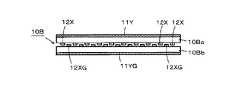
図15の例は、図14の例の上記の問題の改善例である。すなわち、図15の例のセンサ10Bは、2層のセンサ基板10Ba及び10Bbを張り合わせた構成とする。この例では、センサ基板10Baの表面には、複数の第1の導体11Yを形成し、裏面には複数の第2の導体12Xを形成する。また、センサ基板10Bbの表面には、第4の導体12XGを形成し、裏面には第3の導体11YGを形成する。その他の構成は、図14の例と同様とする。 The example of FIG. 15 is an improvement example of the above problem of the example of FIG. That is, the sensor 10B in the example of FIG. 15 has a configuration in which two sensor substrates 10Ba and 10Bb are laminated. In this example, a plurality of
この図15の例によれば、コマンド信号送信及びタッチ検出並びにペン指示検出用の複数の第1の導体11Y及び第2の導体12Xが形成されたセンサ基板10Baと、回路グランドSGとカップリングする複数の第3の導体11YG及び第4の導体12XGとが形成された基板10Bbとは別基板であるので、導体の形成ピッチは、狭くならず、センサ10Bの製造において、導体の形成についての困難性の問題が改善される。 According to the example of FIG. 15, the circuit ground SG is coupled with the sensor substrate 10Ba on which the plurality of
また、回路グランドSGとカップリングするためにセンサ基板10Baとは別の基板10Bbに形成する導体は、図15の例のように、複数の導体とするのではなく、基板Bbの一方の面の全面に一様な導体(この例では光透過性の導体)を形成するようにしてもよい。その場合には、当該基板Bbの全面に形成する導体を一つのスイッチ回路を通じて回路グランドに接続するように構成し、その一つのスイッチ回路を制御回路27により切り替え制御すればよい。そして、この場合には、センサ基板Baに形成されている複数の第1の導体11X及び複数の第2の導体12で使用者の手や指のタッチが検出されたときには、使用者の手や指が基板Bbの一方の面の全面に形成されている導体と静電結合している。そこで、使用者の手や指によるタッチ位置に関係なく、前記一つのスイッチ回路をオンとして、基板Bbの全面に形成されている導体を回路グランドとカップリングするように制御すればよい。すなわち、この場合には、制御回路27は、タッチされた位置がどの位置かを検出して回路グランドとカップリングさせる導体を特定する処理は不要となる。 Further, the conductor formed on the substrate 10Bb different from the sensor substrate 10Ba for coupling with the circuit ground SG is not a plurality of conductors as in the example of FIG. 15, but one surface of the substrate Bb A uniform conductor (a light transmitting conductor in this example) may be formed on the entire surface. In that case, the conductor formed on the entire surface of the substrate Bb may be connected to the circuit ground through one switch circuit, and the one switch circuit may be switched and controlled by the
次に、以上説明したタッチパネルのセンサは、ストライプ状の複数本の導体を、Y方向及びX方向に、互いに交差するように配列したものである。センサ上の導体の構成は、このようなストライプ状の導体からなるものに限られる訳ではない。 Next, in the sensor of the touch panel described above, a plurality of stripe-shaped conductors are arranged so as to cross each other in the Y direction and the X direction. The configuration of the conductors on the sensor is not limited to one composed of such stripe conductors.
図16の例のセンサ10Cは、センサ基板10Ca上に、所定形状、この例では矩形形状の導体片13を、Y方向及びX方向の両方向に、それぞれ複数個ずつ配列する。そして、複数個の導体片13のそれぞれの全ては、グランドセレクタ26Cを通じてマルチプレクサ21Cに接続される。 The
グランドセレクタ26Cは、図3、図4に示したYグランドセレクタ26YやXグランドセレクタ26Xと同様に、複数個の導体片13のそれぞれを、そのままマルチプレクサ21Cに接続させると共に、スイッチ回路をそれぞれ介して回路グランドSGに接続させる構成を備える。グランドセレクタ26Cのそれぞれの導体片13についての各スイッチ回路は、制御回路27Cからの制御信号により切り替え制御される。 Similar to the
マルチプレクサ21Cは、図2に示したコマンド生成回路22、タッチ検出用信号生成回路23、タッチ検出回路24及びペン指示検出回路25と同様の回路を含む送受信回路28Cに接続されている。マルチプレクサ21Cは、この例においては、制御回路27Cからの制御信号を受けて、図5に示したように、時分割で、コマンド送信期間、位置検出期間のタッチ検出期間及びペン指示検出期間のそれぞれの期間において、使用する導体片13を選択するようにする。 The
送受信回路28Cは、コマンド生成回路22、タッチ検出用信号生成回路23、タッチ検出回路24及びペン指示検出回路25と同様の回路により、上述の実施形態と同様の処理動作をする。ただし、この例の場合には、タッチ検出及びペン指示位置検出は、複数個の導体片13のそれぞれについて行われる。そして、送受信回路28Cのタッチ検出結果及びペン指示検出結果が制御回路27Cに供給される。 The transmission / reception circuit 28C performs the same processing operation as that of the above-described embodiment using circuits similar to the
制御回路27Cは、送受信回路28Cからのタッチ検出結果に基づいて、手や指3がタッチしている複数個の導体片13を検出し、その中から回路グランドSGにカップリングする導体片13を選定する。そして、制御回路27Cは、送受信回路28Cからコマンド信号を送出する際には、当該選定したスイッチ回路をオンとする切り替え制御信号を生成して、グランドセレクタ26Cに供給する。 The
したがって、この図16の例においても、前述の実施形態と同様に、アクティブスタイラス4に送信するコマンド信号の強度が低下するのを軽減あるいは防止することができると共に、アクティブスタイラス4において、受信したコマンド信号の強度が低下したり、反転してしまうのを軽減あるいは防止することができる。 Therefore, in the example of FIG. 16 as well as the above-described embodiment, reduction in strength of the command signal transmitted to active stylus 4 can be reduced or prevented, and the command received in active stylus 4 can be reduced. It is possible to reduce or prevent the reduction or inversion of the signal strength.
そして、特に、この図16の例の場合には、導体片13の単位で回路グランドSGとのカップリングが可能である。そのため、コマンド信号の送信時に、回路グランドSGにカップリングしているために送信に寄与しなくなる導体部分を最小限にすることが可能である。 In particular, in the case of the example of FIG. 16, coupling with the circuit ground SG is possible in the unit of the
なお、この図16の例のタッチパネルにおいても、時分割処理ではなく周波数多重処理とすることが可能である。 Also in the touch panel of the example of FIG. 16, it is possible to perform frequency multiplex processing instead of time division processing.
[その他の実施形態及び変形例]
なお、上述の実施形態では、タッチパネルのセンサは、複数の導体が第1の方向(X方向)と、第2の方向(Y方向)との両方向に配列されているものとしたが、いずれか一方の方向に複数の導体が配列されたものであってもよい。[Other Embodiments and Modifications]
In the above-described embodiment, the sensor of the touch panel has a plurality of conductors arranged in both the first direction (X direction) and the second direction (Y direction). A plurality of conductors may be arranged in one direction.
なお、上述の実施形態では、タッチ検出においては拡散符号を用いる方法を説明したが、これに限られるものではなく、周知のその他のタッチ検出方法が適用可能であることは言うまでもない。 In the above-described embodiment, although the method of using the diffusion code has been described in the touch detection, the present invention is not limited to this and it is needless to say that other known touch detection methods can be applied.
なお、上述の実施形態のタッチパネルの例では、電子機器2はバッテリー駆動の場合であったが、AC商用電源で駆動される場合にも、アクティブスタイラスへのタッチパネルからの信号の回り込みの低減を考慮する場合には、AC商用電源で駆動される場合にも有効である。 In the example of the touch panel according to the above-described embodiment, the
また、タッチパネルの回路グランドを外部グランドにカップリングして安定化させることは、前述したように、タッチパネルがACアダプターに接続されてAC商用電源で駆動される場合には、前述したように、この発明によるカップリング制御は不要である。そこで、タッチパネルの回路グランドを外部グランドにカップリングして安定化させる場合を重視する場合において、ACアダプターとバッテリー駆動との両方を電源として用いることができる電子機器に用いられるタッチパネルの場合には、電源として、ACアダプターとバッテリー駆動とのいずれを使用している状態であるのかを判定する回路を備えるようにして、バッテリー駆動のときにのみ、上述した回路グランドへのカップリング制御を行うように構成してもよい。 In addition, as described above, coupling and stabilizing the circuit ground of the touch panel to the external ground is the case where the touch panel is connected to the AC adapter and driven by the AC commercial power source, as described above. The coupling control according to the invention is not necessary. Therefore, in the case of emphasizing the case where the circuit ground of the touch panel is coupled to the external ground for stabilization, in the case of a touch panel used in an electronic device that can use both an AC adapter and battery drive as a power source, It is equipped with a circuit that determines which of the AC adapter and battery drive is in use as a power supply, and coupling control to the circuit ground described above is performed only when the battery is driven. It may be configured.
なお、この発明によるタッチパネルがコマンド信号を静電結合を通じて送信する相手としては、アクティブスタイラス以外であっても、上述と同様にして、コマンド信号の強度の低下を軽減あるいは防止することができるものである。 The other party to which the touch panel according to the present invention transmits the command signal through electrostatic coupling can reduce or prevent the decrease in the strength of the command signal, even if it is other than the active stylus, in the same manner as described above. is there.
なお、上述の実施形態の説明では、アクティブスタイラス4は、芯体をアンテナとして、タッチパネル1からのコマンド信号を受信すると共に、芯体から位置検出用信号をタッチパネルに送信するようにした。しかし、アクティブスタイラスの構成としては、これに限られるものではなく、例えば図17に示すように、アクティブスタイラス4の筐体の芯体41の近傍のスリーブ42を導体により構成し、芯体41とスリーブ42とを用いて、タッチパネル1との信号の送受を行うように構成してもよい。この場合に、芯体41とスリーブ42とのいずれか一方をコマンド信号の受信用、他方を位置検出用信号の送信用とすればよい。 In the above description of the embodiment, the active stylus 4 uses the core as an antenna, receives a command signal from the
なお、上述の実施形態では、タッチ検出された手や指と静電結合している導体を回路グランドに接続するようにしたが、回路グランドではなく、タッチパネルの駆動電源(バッテリー電源を含む)が得られる導体に結合するようにしてもよい。 In the above-described embodiment, the conductor electrostatically coupled to the touch-detected hand or finger is connected to the circuit ground, but the drive power supply (including the battery power supply) of the touch panel is not the circuit ground. You may make it couple | bond with the conductor obtained.
なお、前述もしたが、上述の実施形態の説明における外部グランドとしては、地球電位に限られるものではなく、安定な固定電位であればよい。 As described above, the external ground in the description of the above-described embodiment is not limited to the earth potential, and any stable fixed potential may be used.
1…タッチパネル、4…アクティブスタイラス、10…センサ、11…第1の導体群、12…第2の導体群、20…信号処理回路、21Y…Yマルチセレクタ、21X…Xマルチセレクタ、22…コマンド生成回路、23…タッチ検出用信号生成回路、24…タッチ検出回路、25…ペン指示検出回路、26Y…Yグランドセレクタ、26X…Xグランドセレクタ、27…制御回路
DESCRIPTION OF
Claims (20)
Translated fromJapanese前記タッチパネルとの間での静電結合を介して前記タッチパネルから送信される信号が受信可能に構成された前記アクティブスタイラスに対し、前記静電結合を介して信号を送信する信号送信回路と、
前記アクティブスタイラスとの間での静電結合を介して前記アクティブスタイラスが指示する位置を検出するアクティブスタイラス指示位置検出回路と、
前記使用者の手がタッチされたことを検出するタッチ検出回路と、
前記タッチ検出回路によるタッチ検出結果に対応して、前記タッチパネルに配置された導体であって前記タッチ検出回路でタッチが検出された前記使用者の手と静電結合している導体を前記タッチパネルのグランドへカップリングさせるカップリング制御を行うカップリング制御回路と
を備えていることを特徴とするタッチパネル。A touch panel having a plurality of conductors arranged corresponding to a position detection area, and capable of detecting a position indicated by an active stylus gripped by a user and a touch by the user's hand gripping the active stylus. ,
A signal transmission circuit for transmitting a signal via the electrostatic coupling to the active stylus configured to be capable of receiving a signal transmitted from the touch panel via the electrostatic coupling between the touch panel and the touch panel;
An active stylus pointing position detection circuit that detects a position indicated by the active stylus through capacitive coupling with the active stylus;
A touch detection circuit that detects that the user's hand has been touched;
The conductor disposed on the touch panel corresponding to the touch detection result by the touch detection circuit, the conductor electrostatically coupled to the user's hand whose touch is detected by the touch detection circuit And a coupling control circuit for performing coupling control to be coupled to the ground.
前記タッチ検出回路によって前記使用者の手によるタッチが検出された際には、前記第2の方向に配置された複数の導体の内の、前記使用者の手によるタッチ領域に対応した少なくとも1本の導体が選択的に前記カップリング制御回路によって前記タッチパネルのグランドにカップリングされることを特徴とする請求項1に記載のタッチパネル。The plurality of conductors disposed on the touch panel are disposed in a second direction different from a first direction, and the first direction.
When the touch by the user's hand is detected by the touch detection circuit, at least one of the plurality of conductors arranged in the second direction corresponds to the touch area by the user's hand. The touch panel according to claim 1, wherein the conductor of (4) is selectively coupled to the ground of the touch panel by the coupling control circuit.
前記電気的に独立して配置された導体の内の、前記使用者の手によるタッチ領域に対応したした導体が前記タッチパネルのグランドへカップリングされることを特徴とする請求項1に記載のタッチパネル。The position detection area is provided with a conductor which is disposed electrically independent of the signal transmission to the active stylus and the conductor used for touch detection by the user's hand,
The touch panel according to claim 1, wherein the conductor corresponding to the touch area by the user's hand among the electrically independently disposed conductors is coupled to the ground of the touch panel. .
前記タッチ検出回路によって前記使用者の手によるタッチが検出された際には、前記第1の方向及び前記第2の方向の少なくとも一方の方向に配置された複数の導体の内の、前記使用者の手によるタッチ領域が対応した少なくとも1本の導体が選択的に前記カップリング制御回路によって前記タッチパネルのグランドにカップリングされることを特徴とする請求項1に記載のタッチパネル。The plurality of conductors disposed on the touch panel are disposed in a first direction and a second direction different from the first direction,
When the touch by the user's hand is detected by the touch detection circuit, the user of the plurality of conductors disposed in at least one of the first direction and the second direction. 2. The touch panel according to claim 1, wherein at least one conductor corresponding to a hand touch area is selectively coupled to the ground of the touch panel by the coupling control circuit.
前記タッチパネルとの間での静電結合を介して前記タッチパネルから送信される信号が受信可能に構成された前記アクティブスタイラスに対し、前前記静電結合を介して信号を送信する信号送信回路と、
使用者が把持する前記アクティブスタイラスとの間での静電結合を介して前記アクティブスタイラスが指示する位置を検出するアクティブスタイラス指示位置検出回路と、
前記使用者の手が前記タッチパネルにタッチされたことを検出するタッチ検出回路と、
前記タッチ検出回路によるタッチ検出結果に対応して、前記タッチパネルに配置された導体であって前記タッチ検出回路でタッチが検出された前記使用者の手と静電結合している導体を前記タッチパネルのグランドへカップリングさせるカップリング制御を行うカップリング制御回路と
を備えていることと特徴とする信号処理回路。The touch panel is connected to a plurality of conductors arranged corresponding to the position detection area, and includes a position indicated by an active stylus held by a user and a touch panel for detecting a touch by the user's hand gripping the active stylus. A signal processing device,
A signal transmission circuit for transmitting a signal via the front capacitive coupling to the active stylus configured to be capable of receiving a signal transmitted from the touch panel via the electrostatic coupling between the touch panel and the touch panel;
An active stylus indication position detection circuit for detecting a position indicated by the active stylus through capacitive coupling with the active stylus held by a user;
A touch detection circuit that detects that the user's hand is touched on the touch panel;
The conductor disposed on the touch panel corresponding to the touch detection result by the touch detection circuit, the conductor electrostatically coupled to the user's hand whose touch is detected by the touch detection circuit What is claimed is: 1. A signal processing circuit comprising: a coupling control circuit for performing coupling control for coupling to ground.
前記タッチパネルにはアクティブスタイラスが指示する位置を検出するために、位置検出領域に対応して複数の導体が配置されており、
前記アクティブスタイラスは、前記タッチパネルとの間での静電結合を介して前記タッチパネルから送信される信号が受信可能に構成されており、
使用者の手が前記タッチパネルにタッチされたことを検出し、
前記使用者の手が前記タッチパネルにタッチされたことが検出されたことに対応して、前記タッチパネルに配置された導体であって、前記タッチが検出された前記使用者の手と静電結合している導体を前記タッチパネルのグランドへカップリングさせるカップリング制御を行うようにした
ことを特徴とする回路グランドと外部グランドとのカップリング方法。A ground coupling method of coupling a ground of the signal processing circuit of the touch panel having a signal processing circuit capable of detecting a touch by a hand with an external ground,
In order to detect the position indicated by the active stylus on the touch panel, a plurality of conductors are arranged corresponding to the position detection area,
The active stylus is configured to be capable of receiving a signal transmitted from the touch panel through capacitive coupling with the touch panel,
It detects that the handused for person is touched on the touch panel,
A conductor disposed on the touch panel in response to detection that the user's hand has been touched on the touch panel, and electrostatically coupled to the user's hand from which the touch is detected. Coupling control for coupling the conductor to the ground of the touch panel. A method of coupling a circuit ground and an external ground.
Priority Applications (6)
| Application Number | Priority Date | Filing Date | Title |
|---|---|---|---|
| JP2015246746AJP6532105B2 (en) | 2015-12-17 | 2015-12-17 | Touch panel, signal processing apparatus and ground coupling method |
| TW105133570ATWI705360B (en) | 2015-12-17 | 2016-10-18 | Touch panel, signal processing device, and coupling method |
| US15/351,166US10579183B2 (en) | 2015-12-17 | 2016-11-14 | Touch panel, signal processing device, and coupling method |
| EP16202798.1AEP3182259B1 (en) | 2015-12-17 | 2016-12-08 | Touch panel, signal processing device, and coupling method |
| KR1020160167521AKR102184580B1 (en) | 2015-12-17 | 2016-12-09 | Touch panel, signal processing device, and coupling method |
| CN201611144624.6ACN107066136B (en) | 2015-12-17 | 2016-12-13 | Touch panel, signal processing apparatus and coupling method |
Applications Claiming Priority (1)
| Application Number | Priority Date | Filing Date | Title |
|---|---|---|---|
| JP2015246746AJP6532105B2 (en) | 2015-12-17 | 2015-12-17 | Touch panel, signal processing apparatus and ground coupling method |
Publications (2)
| Publication Number | Publication Date |
|---|---|
| JP2017111687A JP2017111687A (en) | 2017-06-22 |
| JP6532105B2true JP6532105B2 (en) | 2019-06-19 |
Family
ID=57530543
Family Applications (1)
| Application Number | Title | Priority Date | Filing Date |
|---|---|---|---|
| JP2015246746AActiveJP6532105B2 (en) | 2015-12-17 | 2015-12-17 | Touch panel, signal processing apparatus and ground coupling method |
Country Status (6)
| Country | Link |
|---|---|
| US (1) | US10579183B2 (en) |
| EP (1) | EP3182259B1 (en) |
| JP (1) | JP6532105B2 (en) |
| KR (1) | KR102184580B1 (en) |
| CN (1) | CN107066136B (en) |
| TW (1) | TWI705360B (en) |
Families Citing this family (24)
| Publication number | Priority date | Publication date | Assignee | Title |
|---|---|---|---|---|
| KR102523154B1 (en)* | 2016-04-22 | 2023-04-21 | 삼성전자주식회사 | Display apparatus, input device and control method thereof |
| JP6603435B2 (en)* | 2017-02-22 | 2019-11-06 | 株式会社ワコム | Method, sensor controller, and active stylus implemented in a system including an active stylus and a sensor controller |
| JP7267916B2 (en)* | 2017-07-27 | 2023-05-02 | 株式会社ワコム | POSITION DETECTION SENSOR, POSITION DETECTION DEVICE, AND INFORMATION PROCESSING SYSTEM |
| KR102371154B1 (en)* | 2017-09-29 | 2022-03-07 | 엘지디스플레이 주식회사 | Touch display device, touch circuit, active pen, touch system and multi-pen sensing method |
| WO2019097565A1 (en)* | 2017-11-14 | 2019-05-23 | 株式会社ワコム | Sensor controller |
| US20190163292A1 (en)* | 2017-11-28 | 2019-05-30 | Egalax_Empia Technology Inc. | Electronic Board Eraser and Controlling Method Thereof |
| KR102468750B1 (en)* | 2017-12-29 | 2022-11-18 | 엘지디스플레이 주식회사 | Touch display device, touch system, touch driving circuit, and pen sensing method |
| CN119376568A (en)* | 2018-02-13 | 2025-01-28 | 株式会社和冠 | Position detection device and control device |
| TWI678650B (en)* | 2018-06-07 | 2019-12-01 | 李尚禮 | Touch-control sensing device and seneing method for touch-control seneing signal |
| CN111090352B (en)* | 2018-10-24 | 2023-08-15 | 义隆电子股份有限公司 | Touch system, touch device and input device thereof and signal transmission method thereof |
| US10852857B2 (en)* | 2018-11-19 | 2020-12-01 | Sigmasense, Llc. | Frequency diverse e-pen for touch sensor and e-pen systems |
| CN118689321A (en)* | 2019-03-12 | 2024-09-24 | 株式会社和冠 | Touch panel, computer, method for controlling operation of touch panel, and integrated circuit |
| US10739909B1 (en)* | 2019-04-03 | 2020-08-11 | Himax Technologies Limited | Position input system and method |
| CN111831197B (en)* | 2019-04-18 | 2021-10-29 | 奇景光电股份有限公司 | Positioning input system and method |
| JP2021033543A (en)* | 2019-08-22 | 2021-03-01 | 株式会社ワコム | Input device |
| CN110851003B (en)* | 2019-11-19 | 2023-05-12 | 深圳市爱协生科技股份有限公司 | Pen pressure information generation system of active capacitive touch pen |
| US11455054B2 (en) | 2020-03-13 | 2022-09-27 | Microsoft Technology Licensing, Llc | Multi-protocol coexistence in an active stylus |
| US11977702B2 (en) | 2020-03-25 | 2024-05-07 | Microsoft Technology Licensing, Llc. | Uplink channel compensation for touchscreen devices |
| CN113748404B (en)* | 2020-03-31 | 2023-01-10 | 京东方科技集团股份有限公司 | Touch device, touch system and control method thereof |
| EP3920011A1 (en)* | 2020-06-05 | 2021-12-08 | Microsoft Technology Licensing, LLC | Stylus uplink enhancement for touchscreen devices |
| KR20220064473A (en)* | 2020-11-11 | 2022-05-19 | 삼성디스플레이 주식회사 | Display device and driving method thereof |
| US11422663B1 (en) | 2021-05-27 | 2022-08-23 | Stmicroelectronics Asia Pacific Pte Ltd. | Stylus sensing on touchscreens |
| US11656725B2 (en)* | 2021-08-31 | 2023-05-23 | Microsoft Technology Licensing, Llc | Touch-sensing electrode driving for display device |
| US12039125B1 (en) | 2023-04-17 | 2024-07-16 | Ili Technology Corp. | Touch system |
Family Cites Families (26)
| Publication number | Priority date | Publication date | Assignee | Title |
|---|---|---|---|---|
| JPH11249813A (en)* | 1998-03-03 | 1999-09-17 | Sharp Corp | Display-integrated coordinate input device |
| JP3277896B2 (en)* | 1998-07-31 | 2002-04-22 | ぺんてる株式会社 | Capacitance coordinate detection device that also serves as pressure detection |
| KR20050009838A (en)* | 2003-07-18 | 2005-01-26 | 현대자동차주식회사 | monitor with a touch screen improved reflection rate of light |
| EP1892609A4 (en)* | 2005-05-26 | 2013-03-27 | Gunze Kk | Transparent planar body and transparent touch switch |
| CN101655754B (en)* | 2008-08-21 | 2014-03-26 | 株式会社和冠 | Extended touchscreen pattern |
| GB2466566B (en)* | 2008-12-22 | 2010-12-22 | N trig ltd | Digitizer, stylus and method of synchronization therewith |
| JP5295008B2 (en) | 2009-06-18 | 2013-09-18 | 株式会社ワコム | Indicator detection device |
| JP5396167B2 (en) | 2009-06-18 | 2014-01-22 | 株式会社ワコム | Indicator detection apparatus and indicator detection method |
| JP5252454B2 (en)* | 2009-06-30 | 2013-07-31 | 株式会社ジャパンディスプレイウェスト | Contact detection device and display device having touch sensor function |
| JP5429814B2 (en)* | 2010-03-29 | 2014-02-26 | 株式会社ワコム | Indicator detection device and detection sensor |
| CN103534670B (en)* | 2010-10-28 | 2017-02-08 | 谱瑞科技股份有限公司 | Synchronizing a stylus with a capacitive sense array |
| JP5578566B2 (en) | 2010-12-08 | 2014-08-27 | 株式会社ワコム | Indicator detection apparatus and indicator detection method |
| US9116558B2 (en)* | 2011-10-28 | 2015-08-25 | Atmel Corporation | Executing gestures with active stylus |
| US20130300672A1 (en)* | 2012-05-11 | 2013-11-14 | Research In Motion Limited | Touch screen palm input rejection |
| JP6091833B2 (en)* | 2012-10-04 | 2017-03-08 | 株式会社ワコム | Signal processing circuit, signal processing method, position detection apparatus, and electronic apparatus |
| US9158393B2 (en)* | 2012-12-18 | 2015-10-13 | Logitech Europe S.A. | Active stylus for touch sensing applications |
| KR102052371B1 (en)* | 2013-02-01 | 2020-01-08 | 엘지전자 주식회사 | Detachable dual mobile terminal |
| US10459546B2 (en)* | 2013-03-14 | 2019-10-29 | Apple Inc. | Channel aggregation for optimal stylus detection |
| JP5826971B2 (en)* | 2013-04-22 | 2015-12-02 | シャープ株式会社 | Stylus pen, touch panel system, and electronic device |
| KR101282915B1 (en)* | 2013-04-25 | 2013-07-17 | 주식회사 아나패스 | Method for reducing effect of noise and apparatus for detecting touch using the same |
| US10067580B2 (en)* | 2013-07-31 | 2018-09-04 | Apple Inc. | Active stylus for use with touch controller architecture |
| JP6240530B2 (en)* | 2014-02-21 | 2017-11-29 | 株式会社ワコム | Signal processing circuit, signal processing method, position detection device, and electronic apparatus |
| CN204066029U (en)* | 2014-06-23 | 2014-12-31 | 吴凯锋 | Active capacitance pen |
| CN104049778B (en)* | 2014-06-23 | 2017-11-03 | 吴凯锋 | Active capacitance pen |
| KR102521459B1 (en) | 2015-01-19 | 2023-04-14 | 가부시키가이샤 와코무 | Pointing device |
| US9696861B2 (en)* | 2015-03-09 | 2017-07-04 | Stmicroelectronics Asia Pacific Pte Ltd | Touch rejection for communication between a touch screen device and an active stylus |
- 2015
- 2015-12-17JPJP2015246746Apatent/JP6532105B2/enactiveActive
- 2016
- 2016-10-18TWTW105133570Apatent/TWI705360B/enactive
- 2016-11-14USUS15/351,166patent/US10579183B2/enactiveActive
- 2016-12-08EPEP16202798.1Apatent/EP3182259B1/enactiveActive
- 2016-12-09KRKR1020160167521Apatent/KR102184580B1/enactiveActive
- 2016-12-13CNCN201611144624.6Apatent/CN107066136B/enactiveActive
Also Published As
| Publication number | Publication date |
|---|---|
| CN107066136B (en) | 2021-07-09 |
| TW201727454A (en) | 2017-08-01 |
| CN107066136A (en) | 2017-08-18 |
| EP3182259B1 (en) | 2019-01-30 |
| KR20170072795A (en) | 2017-06-27 |
| US10579183B2 (en) | 2020-03-03 |
| TWI705360B (en) | 2020-09-21 |
| US20170177145A1 (en) | 2017-06-22 |
| EP3182259A1 (en) | 2017-06-21 |
| KR102184580B1 (en) | 2020-12-01 |
| JP2017111687A (en) | 2017-06-22 |
Similar Documents
| Publication | Publication Date | Title |
|---|---|---|
| JP6532105B2 (en) | Touch panel, signal processing apparatus and ground coupling method | |
| CN110892368B (en) | Sensor Controller | |
| JP6472196B2 (en) | Sensor signal processing circuit and sensor signal processing method | |
| KR102358217B1 (en) | Stylus tilt detection based on bidirectional communication between stylus and stylus sensor controller | |
| EP2518603B1 (en) | Multi-touch and multi-user detecting device | |
| US9958966B2 (en) | Active stylus communication and position system | |
| CA2809038C (en) | System for an electrostatic stylus within a capacitive touch sensor | |
| CN102109923B (en) | Pointing body, position detection device and position detection method | |
| US20160041677A1 (en) | Position detecting unit | |
| CN106201049B (en) | Position detection device and position detection method | |
| CN104714707B (en) | Electromagnetic and capacitance integrated touch screen, touch display panel and touch display device | |
| US9841862B2 (en) | Stylus position system | |
| TW201201084A (en) | Position detection apparatus | |
| KR20200119794A (en) | Position detection device and position detection method based on electromagnetic inductive coupling and electrostatic coupling | |
| TWI621038B (en) | Wired stylus, touch sensitive electronic device and system and method thereof | |
| KR101830981B1 (en) | Sensing apparatus for sensing position of touch object based on electromagnetic induction and method for controlling thereof | |
| KR20160052928A (en) | Touch display device for energy harvesting | |
| KR102773715B1 (en) | Touch sensor and touch input device thereof | |
| US10031590B2 (en) | Active stylus with a parallel communication channel | |
| JP2014106743A (en) | Electric tactile sense presentation device, control method and program for electric tactile sense presentation device, and portable equipment with electric tactile sense display | |
| KR102007690B1 (en) | Position sensing apparatus for sensing position of pen and method for controlling thereof | |
| JP2017102894A (en) | Detection device |
Legal Events
| Date | Code | Title | Description |
|---|---|---|---|
| A621 | Written request for application examination | Free format text:JAPANESE INTERMEDIATE CODE: A621 Effective date:20181022 | |
| A131 | Notification of reasons for refusal | Free format text:JAPANESE INTERMEDIATE CODE: A131 Effective date:20190410 | |
| A977 | Report on retrieval | Free format text:JAPANESE INTERMEDIATE CODE: A971007 Effective date:20190410 | |
| A521 | Request for written amendment filed | Free format text:JAPANESE INTERMEDIATE CODE: A523 Effective date:20190425 | |
| TRDD | Decision of grant or rejection written | ||
| A01 | Written decision to grant a patent or to grant a registration (utility model) | Free format text:JAPANESE INTERMEDIATE CODE: A01 Effective date:20190515 | |
| A61 | First payment of annual fees (during grant procedure) | Free format text:JAPANESE INTERMEDIATE CODE: A61 Effective date:20190516 | |
| R150 | Certificate of patent or registration of utility model | Ref document number:6532105 Country of ref document:JP Free format text:JAPANESE INTERMEDIATE CODE: R150 | |
| R250 | Receipt of annual fees | Free format text:JAPANESE INTERMEDIATE CODE: R250 | |
| R250 | Receipt of annual fees | Free format text:JAPANESE INTERMEDIATE CODE: R250 | |
| R250 | Receipt of annual fees | Free format text:JAPANESE INTERMEDIATE CODE: R250 | |
| R250 | Receipt of annual fees | Free format text:JAPANESE INTERMEDIATE CODE: R250 |