JP6528517B2 - Method of applying alignment film - Google Patents
Method of applying alignment filmDownload PDFInfo
- Publication number
- JP6528517B2 JP6528517B2JP2015077368AJP2015077368AJP6528517B2JP 6528517 B2JP6528517 B2JP 6528517B2JP 2015077368 AJP2015077368 AJP 2015077368AJP 2015077368 AJP2015077368 AJP 2015077368AJP 6528517 B2JP6528517 B2JP 6528517B2
- Authority
- JP
- Japan
- Prior art keywords
- alignment film
- substrate
- wettability
- transfer plate
- liquid crystal
- Prior art date
- Legal status (The legal status is an assumption and is not a legal conclusion. Google has not performed a legal analysis and makes no representation as to the accuracy of the status listed.)
- Active
Links
Images


Classifications
- G—PHYSICS
- G02—OPTICS
- G02F—OPTICAL DEVICES OR ARRANGEMENTS FOR THE CONTROL OF LIGHT BY MODIFICATION OF THE OPTICAL PROPERTIES OF THE MEDIA OF THE ELEMENTS INVOLVED THEREIN; NON-LINEAR OPTICS; FREQUENCY-CHANGING OF LIGHT; OPTICAL LOGIC ELEMENTS; OPTICAL ANALOGUE/DIGITAL CONVERTERS
- G02F1/00—Devices or arrangements for the control of the intensity, colour, phase, polarisation or direction of light arriving from an independent light source, e.g. switching, gating or modulating; Non-linear optics
- G02F1/01—Devices or arrangements for the control of the intensity, colour, phase, polarisation or direction of light arriving from an independent light source, e.g. switching, gating or modulating; Non-linear optics for the control of the intensity, phase, polarisation or colour
- G02F1/13—Devices or arrangements for the control of the intensity, colour, phase, polarisation or direction of light arriving from an independent light source, e.g. switching, gating or modulating; Non-linear optics for the control of the intensity, phase, polarisation or colour based on liquid crystals, e.g. single liquid crystal display cells
- G02F1/133—Constructional arrangements; Operation of liquid crystal cells; Circuit arrangements
- G02F1/1333—Constructional arrangements; Manufacturing methods
- G02F1/1337—Surface-induced orientation of the liquid crystal molecules, e.g. by alignment layers
- B—PERFORMING OPERATIONS; TRANSPORTING
- B05—SPRAYING OR ATOMISING IN GENERAL; APPLYING FLUENT MATERIALS TO SURFACES, IN GENERAL
- B05D—PROCESSES FOR APPLYING FLUENT MATERIALS TO SURFACES, IN GENERAL
- B05D1/00—Processes for applying liquids or other fluent materials
- B05D1/28—Processes for applying liquids or other fluent materials performed by transfer from the surfaces of elements carrying the liquid or other fluent material, e.g. brushes, pads, rollers
- B05D1/286—Processes for applying liquids or other fluent materials performed by transfer from the surfaces of elements carrying the liquid or other fluent material, e.g. brushes, pads, rollers using a temporary backing to which the coating has been applied
- C—CHEMISTRY; METALLURGY
- C09—DYES; PAINTS; POLISHES; NATURAL RESINS; ADHESIVES; COMPOSITIONS NOT OTHERWISE PROVIDED FOR; APPLICATIONS OF MATERIALS NOT OTHERWISE PROVIDED FOR
- C09K—MATERIALS FOR MISCELLANEOUS APPLICATIONS, NOT PROVIDED FOR ELSEWHERE
- C09K2323/00—Functional layers of liquid crystal optical display excluding electroactive liquid crystal layer characterised by chemical composition
- C09K2323/06—Substrate layer characterised by chemical composition
Landscapes
- Physics & Mathematics (AREA)
- Nonlinear Science (AREA)
- Mathematical Physics (AREA)
- Chemical & Material Sciences (AREA)
- Crystallography & Structural Chemistry (AREA)
- General Physics & Mathematics (AREA)
- Optics & Photonics (AREA)
- Spectroscopy & Molecular Physics (AREA)
- Liquid Crystal (AREA)
- Optical Filters (AREA)
Description
Translated fromJapanese本発明は、液晶パネルを構成するガラス基板上に配向膜を塗布する方法、およびそれに用いるカラーフィルタ基板に関するものである。 The present invention relates to a method of applying an alignment film on a glass substrate constituting a liquid crystal panel, and a color filter substrate used therefor.
近年、液晶パネル等のFPD(Flat Panel Display)はその軽量、薄型、低消費電力化が進み、テレビ、カーナビゲーション機器、コンピュータを始めとして多くの分野で利用されている。そのパネルサイズは年々大型化、高精細化が進んでいるものの、用途によりさまざまな形や大きさが要求されている。液晶パネルの多品種少量生産への対応は必要不可欠である。 In recent years, flat panel displays (FPDs) such as liquid crystal panels have become lighter, thinner, and lower in power consumption, and are used in many fields including television, car navigation devices, and computers. Although the panel size is increasing year by year and high definition is in progress, various shapes and sizes are required depending on the application. Correspondence to high-mix low-volume production of liquid crystal panels is essential.
液晶パネルは互いに対向する一対の基板を有し、基板間がスペーサーによって一定に挟持されており、その基板間は液晶が満たされている。一方の基板は薄膜ドランジスタ(TFT)を形成したアクティブマトリクス型の基板(以後、TFT基板と称す)であり、他方の対向基板はカラーフィルタ基板(以後、CF基板と称す)である。それぞれの基板上には導電膜が形成されており、互いの導電膜間において蓄えられた電荷により、液晶を駆動制御している。 The liquid crystal panel has a pair of substrates facing each other, and between the substrates is held constant by a spacer, and the space between the substrates is filled with liquid crystal. One of the substrates is an active matrix type substrate (hereinafter referred to as a TFT substrate) on which thin film transistors (TFTs) are formed, and the other opposing substrate is a color filter substrate (hereinafter referred to as a CF substrate). A conductive film is formed on each substrate, and the liquid crystal is driven and controlled by the charge stored between the conductive films.
TFT基板のトランジスタ形成部や配線部の液晶の駆動は、表示部のそれと比較して制御することが困難であり、対向CF基板側に遮蔽領域を形成し、光の透過を抑制することで、美しい表示が可能となる。 Driving of the liquid crystal in the transistor formation portion and the wiring portion of the TFT substrate is difficult to control as compared to that of the display portion, and a shielding region is formed on the opposite CF substrate side to suppress light transmission. Beautiful display is possible.
液晶パネルは光を透過させる領域においては、液晶分子を均一に配列させる必要がある。液晶分子に電圧をかけることで、液晶分子の配列方向を変化させ、光の通る方向をコントロールする。そのためにはTFT基板およびCF基板表面に配向膜を均一に塗布し、表面をラビング布で擦る処理を行う必要がある。 In a liquid crystal panel, it is necessary to arrange liquid crystal molecules uniformly in a region where light is transmitted. By applying a voltage to the liquid crystal molecules, the alignment direction of the liquid crystal molecules is changed to control the light passing direction. For this purpose, it is necessary to uniformly apply an alignment film on the surfaces of the TFT substrate and the CF substrate and rubbing the surface with a rubbing cloth.
配向膜の塗布にはノズルから配向膜を吹き付ける方式(特許文献1)と、転写版を使用した印刷方式(特許文献2、3)がある。前者は品種毎の版は必要ないが、ノズルからの噴射ムラが発生しやすく膜厚の均一性のコントロールが難しい。特に高精細なパネルにおいて、配向膜膜厚の不均一は致命的である。一方、後者は膜厚を均一にしやすいが、多品種を製造する際、品種毎にパターンニングした転写版(特許文献2、段落0004または特許文献3、段落0031ほか)が必要となる。 There are a system (patent document 1) which sprays an alignment film from a nozzle, and a printing system (
上記配向膜転写工程において、液晶パネルのガラス基板に配向膜を塗布する際、主に表示領域となる配向膜を塗布する領域と、表示領域の周辺部となる配向膜を塗布しない領域とを塗り分けて形成する必要が生じる。配向膜を塗布しない領域は、上層に液晶パネルの周辺シール材や実装部材を取り付ける領域や検査で針を接触させる検査端子を配置する領域等である。 When the alignment film is applied to the glass substrate of the liquid crystal panel in the alignment film transfer step, the area to be coated with the alignment film mainly serving as the display area and the area not coated with the alignment film to be peripheral to the display area are coated It will be necessary to form separately. The area where the alignment film is not applied is an area where the peripheral sealing material or mounting member of the liquid crystal panel is attached to the upper layer, an area where an inspection terminal for contacting a needle in an inspection, etc. is disposed.
すなわち、液晶パネルのシール材を配向膜上に塗布すると、密着力の低下を招くため、配向膜を塗布しない。また、実装部材を取り付ける領域や検査で針を接触させる検査端子に配向膜を塗布すると、抵抗値が変化し、液晶パネルの駆動が困難となる。このように配向膜を塗布しない領域を形成する必要が生じ、配向膜膜厚を均一化しやすい配向膜転写方式においては、多品種を製造する際、品種毎に配向膜を塗布する領域と塗布しない領域を塗り分けるための転写版が必要となる。 That is, when the sealing material of the liquid crystal panel is applied on the alignment film, the adhesion is lowered, and thus the alignment film is not applied. In addition, when an alignment film is applied to an area where the mounting member is to be attached or an inspection terminal with which the needle is brought into contact in an inspection, the resistance value changes, which makes it difficult to drive the liquid crystal panel. As described above, in the alignment film transfer method in which it is necessary to form an area in which the alignment film is not applied and it is easy to make the film thickness of the alignment film uniform, when manufacturing various types, the area in which the alignment film is applied is not applied A transfer plate is needed to paint the area separately.
したがって配向膜転写方式では、配向膜塗布工程において液晶パネルの品種毎の転写版の管理が必要になり、保管場所や品種毎の設計と製作が必要となる。また仮に転写版に不具合が生じても、他品種の転写版では代用できないため、各品種毎に複数の転写版が必要になる。それ故さらなる管理コストが生じてしまう。さらに、製品生産時、配向膜塗布工程において、転写版は品種毎に版の取替え作業が必要になるため、生産稼動時のロスが発生する。 Therefore, in the alignment film transfer method, management of the transfer plate for each type of liquid crystal panel is required in the alignment film application step, and design and manufacture for each storage location and type are required. In addition, even if a defect occurs in the transfer plate, the transfer plate of other types can not be substituted, so a plurality of transfer plates are required for each type. Therefore, additional management costs arise. Furthermore, during the production of the product, since the transfer plate needs to be replaced for each type in the alignment film coating step, a loss occurs during production operation.
本発明では、多品種のインチサイズや、液晶パネルのガラス基板における面付けの異なる品種、特に端子の無いCF基板の配向膜塗布工程において、配向膜の膜厚を均一に形成し、且つ配向膜転写工程における転写版の製作や管理の簡素化と、生産品種の切り替え毎に生ずる段取り替え作業による生産稼動時間のロスを減らす。 In the present invention, the film thickness of the alignment film is uniformly formed in the alignment film application step of the various types of inch sizes and the imposition different on the glass substrate of the liquid crystal panel, particularly the terminal-free CF substrate, and the alignment film Simplify the production and management of transfer plates in the transfer process and reduce the loss of production operation time due to the setup change operation that occurs each time the product type is switched.
この発明に係る配向膜の塗布方法は、塗布対象の基板が、配向膜を塗布する面において、前記配向膜の材料に対して濡れ性の大きい表面と、濡れ性の小さい表面とに区分されており、 転写版を用いて前記基板に配向膜を塗布する際に、前記濡れ性の大きい表面と前記濡れ性の小さい表面とも一様に前記配向膜材料が接触する工程と、 前記転写版と前記基板の表面を分離する工程とを備え、 その分離工程を経て、前記濡れ性の大きい表面に前記配向膜材料が残り、前記濡れ性の小さい表面には前記配向膜材料が残らないことを特徴とする。 In the method for applying the alignment film according to the present invention, the substrate to be coated is divided into a surface having high wettability to the material of the alignment film and a surface having low wettability on the surface to which the alignment film is applied. When applying an alignment film to the substrate using a transfer plate, the alignment film material is uniformly brought into contact with the surface with high wettability and the surface with low wettability as well; And separating the surface of the substrate, wherein the alignment film material remains on the surface with high wettability after the separation step, and the alignment film material does not remain on the surface with low wettability. Do.
本発明によれば、複数種の転写版が不要になり、その管理コストが減少する。さらに配向膜塗布工程において、品種毎に転写版の段取り変え作業が不要になるため、生産性が向上する。 According to the present invention, plural types of transfer plates are not required, and the management cost is reduced. Furthermore, in the alignment film coating process, since the work of changing the transfer plate setup for each product type is not necessary, the productivity is improved.
以下、本発明の実施の形態について図面を参照しながら説明する。なお、説明が重複して冗長になるのを避けるため、各図において同一または相当する機能を有する要素には同一の符号を付してある。 Hereinafter, embodiments of the present invention will be described with reference to the drawings. In addition, in order to avoid duplication of description and becoming redundant, the same code | symbol is attached | subjected to the element which has the same or equivalent function in each figure.
実施の形態1.
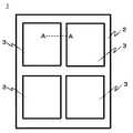
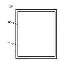
以下、この発明の実施の形態1を図面を参照しながら詳細に説明する。図1は、上述の互いに対向する一対の基板から構成される液晶パネルの一方の基板であるCF基板の平面模式図である。また本実施の形態では、他方の基板であるTFT基板は一般的なTN液晶モードに対応したTFT基板を採用しているので、特に詳細な説明はしない。図2は、図1の断面模式図であり、上記のように液晶パネルがTN液晶モードに対応した断面構造を有している。図3は本発明で使用する配向膜転写版の平面模式図であり、さらに図4は本発明での配向膜塗布状態を表す模式図である。
Hereinafter,
<CF基板の構成>
まず、図1に示す様に、CF基板1は、その表面が予め濡れ性(wettability)の低い領域2と、濡れ性の大きい領域3に区別されて作成される。すなわち本実施の形態では、CF基板1の表面を形成する際に、濡れ性の小さい領域2は、配向膜を塗布しない領域に対応して、また濡れ性の大きい領域3は、配向膜を塗布する領域に対応して形成される。なお、ここで言う基板表面の「濡れ性」とは、配向膜材料に対する「濡れ性」の大/小(良い/悪い)を意味する。<Configuration of CF substrate>
First, as shown in FIG. 1, the
図2は図1の破線部分A−A間における断面図である。図2に示す様に濡れ性の大きい領域3の縦構造として、ガラス基板4の上層には、下層から順に、遮光層である遮蔽領域5、透過層の色材6、導電膜7が積層された状態である。表示領域の導電膜7は、濡れ性の大きい透明膜である必要があり、画素を構成する対向電極材料としてITO膜やIGZO膜を用いるのが適当である。 FIG. 2 is a cross-sectional view taken along the broken line portion A-A of FIG. As shown in FIG. 2, as a vertical structure of the
一方、表示領域の周辺部となる濡れ性の小さい領域2の縦構造として、ガラス基板4上に濡れ性の小さい有機膜8を形成する。有機膜8の表面は、配向膜をはじく撥油性を持つ必要があり、有機膜8の表面9は、微細な凹凸の多い状態である。材料として有機フッ化物や光硬化型樹脂のアクリル樹脂やポリイミド樹脂等を用いるのが適当である。 On the other hand, an
<配向膜塗布工程>
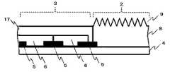
まず、配向膜を塗布する際に必要となる転写版の構成について説明する。図3に示すように配向膜を塗布する転写版10は、転写版下地11上に配向膜材料を塗る転写版凸部12で構成されている。転写版材料としてはポリブタジエンゴム等を用いる。転写版凸部12には配向膜13を付着させる領域と付着させない領域を区分する凹部は無く、一様なベタパターンである。<Alignment film coating process>
First, the configuration of the transfer plate required to apply the alignment film will be described. As shown in FIG. 3, the
次に、図4の配向膜塗布模式図に示すように、印刷方式でCF基板1に配向膜材料16を塗布する場合、転写装置胴体14に取り付けられた転写版10の転写版凸部12の表面に、配向膜供給ノズル15より配向膜材料16を滴下し付着させる。 Next, as shown in the alignment film application schematic diagram of FIG. 4, when the
配向膜塗布工程では、転写装置胴体14に巻き付けられた転写版10と、CF基板1が位置合わせされたのち、転写装置胴体14が黒矢印方向に回転するのと同期して、CF基板1を保持するステージ(非図示)が白矢印方向に移動して、転写版凸部12がCF基板1の端部から順に接触してゆき、転写作業が行われる。In the alignment film coating step, after the
上述したようにCF基板1表面には濡れ性の小さい領域2と濡れ性の大きい領域3が存在する。上述のように転写版凸部12がCF基板1表面に接触した時、転写版凸部12に付着している配向膜材料16は、濡れ性の小さい領域2と濡れ性の大きい領域3いずれにも接触することになる。しかし、配向膜材料16は、上記CF基板1の移動に伴って、転写版凸部12がCF基板1から分離した後は、配向膜材料16は濡れ性の違いで選択的に領域3にのみ付着する。一方濡れ性の小さい領域2に一旦接触した配向膜材料16は、CF基板1に付着することなく、転写版凸部12側に残ることになる。 As described above, the
なお、図4では、転写版凸部12とCF基板1は一定の距離を持って描かれているが、これは、濡れ性の小さい領域2と濡れ性の大きい領域3の区別を分かりやすくするための誇張であり、実際は上述のように配向膜材料16を介して接触している。 In FIG. 4, the transfer plate
CF基板1上に残った配向膜材料16は、その後の乾燥、焼成などの通常の工程を経て配向膜13となり、CF基板1上に選択的に形成される。 The
実施の形態2.
本実施の形態では、上記他方の基板であるTFT基板は一般的なIPS液晶モードに対応したTFT基板を採用しているので、特に詳細な説明はしない。その他、CF基板1の平面図(図1)や、配向膜転写版(図3)、配向膜塗布模工程(図4)などは、上述の実施の形態1と同様であるので、詳細な説明は省略する。Second Embodiment
In the present embodiment, a TFT substrate corresponding to a general IPS liquid crystal mode is adopted as the TFT substrate which is the other substrate described above, and thus the detailed description will not be made. In addition, the plan view of the CF substrate 1 (FIG. 1), the alignment film transfer plate (FIG. 3), the alignment film coating simulation step (FIG. 4), and the like are the same as in the first embodiment described above. Is omitted.
図5は、CF基板の断面模式図であり、上記のようにIPS液晶モードに対応した断面構造となっており、画素部において対向電極が無い。また、図5は、上述の実施の形態と同様に図1の破線部分A−A間における断面図である。
Figure 5 is a schematic cross-sectional view of a CF substrate, has a cross-sectional structure corresponding to IPS liquid crystal mode as described above, there is no Oite counter electrodein the pixel portion. Moreover, FIG. 5 is a cross-sectional view between broken line portions A-A in FIG. 1 as in the above-described embodiment.
図5に示す様に濡れ性の大きい領域3の縦構造として、ガラス基板4の上層には、下層から順に、遮光層である遮蔽領域5、透過層の色材6、濡れ性の大きい有機膜17が積層された状態である。 As shown in FIG. 5, as the vertical structure of the
濡れ性の大きい有機膜17は、主に表示領域に形成されるので透明膜である必要があり、材料としては熱硬化型のアクリル樹脂やポリイミド樹脂が望ましい。一方、濡れ性の小さい領域2の縦構造として、ガラス基板4上には濡れ性の小さい有機膜8を形成する。有機膜8の表面9は、配向膜材料16をはじく撥油性が必要であり、有機膜の表面9は、微細な凹凸の多い状態である。材料として有機フッ化物や光硬化型樹脂のアクリル樹脂やポリイミド樹脂等を用いるのが適当である。 The
また、上記実施の形態1または2にて示したCF基板1では、濡れ性の小さい領域2において、ガラス基板4上に濡れ性の小さい有機膜8を形成すると説明したが、有機膜8に使用する材料自体が持つ濡れ性は特に問題ではなく、その表面9の濡れ性が低ければよい。比較的濡れ性が高い有機材料を塗布した後で、フッ素加工などの表面処理や、ナノチューブなど表面に微細突起を有する凹凸構造を施して濡れ性の小さい有機膜の表面9を実現してもよい。 In the
上述の実施の形態1または2においては、液晶パネルを構成する互いに対向する一対の基板のうち、一方の基板であるCF基板を例示して、ガラス基板上の濡れ性の領域分けによる配向膜の塗り分けを説明したが、上記領域分けを施す基板は、CF基板である必要はなく、液晶パネルの他方の基板であるTFT基板であってもよいのは無論である。 In the first or second embodiment described above, the CF substrate which is one of the pair of substrates facing each other constituting the liquid crystal panel is exemplified, and the alignment film is divided into regions by wettability on the glass substrate. Although different coating has been described, the substrate to which the above-described area division is applied does not have to be a CF substrate, and it goes without saying that it may be a TFT substrate which is the other substrate of the liquid crystal panel.
1 CF基板、2 濡れ性の小さい領域、3 濡れ性の大きい領域、4 ガラス基板、7 導電膜、8 濡れ性の小さい有機膜、9 有機膜の表面、10 転写版、13 配向膜、16 配向膜材料、17 濡れ性の大きい有機膜1 CF substrate, 2 area with low wettability, 3 area with high wettability, 4 glass substrate, 7 conductive film, 8 organic film with low wettability, 9 surface of organic film, 10 transfer plate, 13 alignment film, 16 alignment Film material, 17 high wettability organic film
Claims (4)
Translated fromJapanese前記基板は、配向膜を塗布する面が、前記配向膜の材料に対して濡れ性の大きい表面と、濡れ性の小さい表面とに区分されており、
転写版を用いて前記基板に前記配向膜の材料を塗布する際に、前記濡れ性の大きい表面と前記濡れ性の小さい表面とも一様に前記配向膜材料が接触する工程と、
前記転写版と前記基板の表面を分離する工程とを備え、
前記分離工程を経て、前記濡れ性の大きい表面に前記配向膜材料が残り、前記濡れ性の小さい表面には前記配向膜の材料が残らないことを特徴とする配向膜の塗布方法。A method of applying an alignment film to a substrate of a liquid crystal panel,
In the substrate, the surface to which the alignment film is applied is divided into a surface having high wettability to the material of the alignment film and a surface having low wettability.
When the material of the alignment film is applied to the substrate using a transfer plate, the alignment film material uniformly contacts the surface with high wettability and the surface with low wettability;
Separating the transfer plate and the surface of the substrate;
After the separation step, the alignment film material remains on the surface with high wettability, and the material of the alignment film does not remain on the surface with low wettability.
Priority Applications (3)
| Application Number | Priority Date | Filing Date | Title |
|---|---|---|---|
| JP2015077368AJP6528517B2 (en) | 2015-04-06 | 2015-04-06 | Method of applying alignment film |
| US15/078,089US20160291360A1 (en) | 2015-04-06 | 2016-03-23 | Method of applying alignment film, and color filter substrate |
| US16/906,303US11067854B2 (en) | 2015-04-06 | 2020-06-19 | Method of applying alignment film, and color filter substrate |
Applications Claiming Priority (1)
| Application Number | Priority Date | Filing Date | Title |
|---|---|---|---|
| JP2015077368AJP6528517B2 (en) | 2015-04-06 | 2015-04-06 | Method of applying alignment film |
Publications (3)
| Publication Number | Publication Date |
|---|---|
| JP2016197190A JP2016197190A (en) | 2016-11-24 |
| JP2016197190A5 JP2016197190A5 (en) | 2018-04-19 |
| JP6528517B2true JP6528517B2 (en) | 2019-06-12 |
Family
ID=57015895
Family Applications (1)
| Application Number | Title | Priority Date | Filing Date |
|---|---|---|---|
| JP2015077368AActiveJP6528517B2 (en) | 2015-04-06 | 2015-04-06 | Method of applying alignment film |
Country Status (2)
| Country | Link |
|---|---|
| US (2) | US20160291360A1 (en) |
| JP (1) | JP6528517B2 (en) |
Cited By (1)
| Publication number | Priority date | Publication date | Assignee | Title |
|---|---|---|---|---|
| US11067854B2 (en)* | 2015-04-06 | 2021-07-20 | Mitsubishi Electric Corporation | Method of applying alignment film, and color filter substrate |
Families Citing this family (2)
| Publication number | Priority date | Publication date | Assignee | Title |
|---|---|---|---|---|
| CN107329326A (en)* | 2017-07-27 | 2017-11-07 | 武汉华星光电技术有限公司 | Transfer printing board and transfer device |
| CN111367124B (en) | 2020-02-12 | 2021-06-01 | 武汉华星光电技术有限公司 | Alignment film transfer plate and alignment film manufacturing method |
Family Cites Families (25)
| Publication number | Priority date | Publication date | Assignee | Title |
|---|---|---|---|---|
| JP3901679B2 (en) | 1992-09-17 | 2007-04-04 | セイコーエプソン株式会社 | Tension development film forming equipment |
| US5558927A (en) | 1992-09-17 | 1996-09-24 | Seiko Epson Corporation | Color filter for liquid crystal displays and film-forming apparatus |
| JP3092896B2 (en) | 1993-09-28 | 2000-09-25 | シャープ株式会社 | Liquid crystal display device and method of manufacturing the same |
| TW291543B (en) | 1993-09-28 | 1996-11-21 | Sharp Kk | |
| JP3267844B2 (en) | 1994-11-09 | 2002-03-25 | シャープ株式会社 | Liquid crystal element and manufacturing method thereof |
| CN100485904C (en)* | 1996-09-19 | 2009-05-06 | 精工爱普生株式会社 | Matrix type display device and manufacturing method thereof |
| JPH1192659A (en) | 1997-09-25 | 1999-04-06 | Hitachi Chem Co Ltd | Printing resin composition and method for producing patterned printing resin film |
| JPH11119221A (en) | 1997-10-13 | 1999-04-30 | Sanyo Electric Co Ltd | Production of liquid crystal display device |
| JP2003005186A (en) | 2001-06-20 | 2003-01-08 | Nec Corp | Method for manufacturing liquid crystal display device and coated film drying device |
| JP2004341336A (en) | 2003-05-16 | 2004-12-02 | Seiko Epson Corp | Liquid crystal device, method of manufacturing the same, and electronic equipment |
| JP5093985B2 (en) | 2004-01-16 | 2012-12-12 | 株式会社半導体エネルギー研究所 | Method for forming a film pattern |
| US8053171B2 (en) | 2004-01-16 | 2011-11-08 | Semiconductor Energy Laboratory Co., Ltd. | Substrate having film pattern and manufacturing method of the same, manufacturing method of semiconductor device, liquid crystal television, and EL television |
| TW200628938A (en)* | 2005-02-02 | 2006-08-16 | Quanta Display Inc | Substrate of a liquid crystal display and method of forming an alignment layer |
| KR101209046B1 (en)* | 2005-07-27 | 2012-12-06 | 삼성디스플레이 주식회사 | Thin film transistor substrate and method of making thin film transistor substrate |
| JP4768393B2 (en)* | 2005-10-21 | 2011-09-07 | Nec液晶テクノロジー株式会社 | Liquid crystal display device and manufacturing method thereof |
| JP4039456B2 (en) | 2006-11-17 | 2008-01-30 | セイコーエプソン株式会社 | Liquid crystal panel and manufacturing method thereof |
| JP4869892B2 (en)* | 2006-12-06 | 2012-02-08 | 株式会社 日立ディスプレイズ | Liquid crystal display |
| JP2008158344A (en)* | 2006-12-25 | 2008-07-10 | Lg Display Co Ltd | Manufacturing method of liquid crystal display panel |
| JP2008185904A (en)* | 2007-01-31 | 2008-08-14 | Toppan Printing Co Ltd | Method for forming projection for controlling liquid crystal alignment |
| JP5046014B2 (en)* | 2007-09-13 | 2012-10-10 | Nltテクノロジー株式会社 | Color filter substrate and liquid crystal display device |
| US8629969B2 (en)* | 2007-11-08 | 2014-01-14 | Gold Charm Limited | Liquid crystal display panel and method of manufacturing the liquid crystal display panel |
| US8431426B1 (en)* | 2011-11-15 | 2013-04-30 | Shenzhen China Star Optoelectronics Technology Co., Ltd. | Coating method for liquid crystal alignment film of TFT-LCD |
| JP6275418B2 (en)* | 2013-09-03 | 2018-02-07 | 株式会社ジャパンディスプレイ | Liquid crystal display |
| CN103777384A (en)* | 2014-01-29 | 2014-05-07 | 北京京东方光电科技有限公司 | Manufacturing method of display panel and transfer printing plate |
| JP6528517B2 (en)* | 2015-04-06 | 2019-06-12 | 三菱電機株式会社 | Method of applying alignment film |
- 2015
- 2015-04-06JPJP2015077368Apatent/JP6528517B2/enactiveActive
- 2016
- 2016-03-23USUS15/078,089patent/US20160291360A1/ennot_activeAbandoned
- 2020
- 2020-06-19USUS16/906,303patent/US11067854B2/enactiveActive
Cited By (1)
| Publication number | Priority date | Publication date | Assignee | Title |
|---|---|---|---|---|
| US11067854B2 (en)* | 2015-04-06 | 2021-07-20 | Mitsubishi Electric Corporation | Method of applying alignment film, and color filter substrate |
Also Published As
| Publication number | Publication date |
|---|---|
| JP2016197190A (en) | 2016-11-24 |
| US20200319486A1 (en) | 2020-10-08 |
| US11067854B2 (en) | 2021-07-20 |
| US20160291360A1 (en) | 2016-10-06 |
Similar Documents
| Publication | Publication Date | Title |
|---|---|---|
| US7262823B2 (en) | Display device and manufacturing method thereof | |
| CN100498549C (en) | Apparatus for fabricating flat panel display device and method of fabricating the same | |
| US11067854B2 (en) | Method of applying alignment film, and color filter substrate | |
| JP5464638B2 (en) | Display element | |
| KR101339170B1 (en) | Liquid crystal display panel and manufacturing method thereof | |
| US20130148067A1 (en) | Array substrate, liquid crystal panel and liquid crystal display device | |
| US8179515B2 (en) | Apparatus and method for manufacturing liquid crystal display panel | |
| US10464365B2 (en) | Alignment film printing plate and manufacturing method thereof | |
| JP2015087650A (en) | Liquid crystal display device and manufacturing method thereof | |
| CN109946863A (en) | A mask and method of making the same | |
| JP6813987B2 (en) | Manufacturing method of electrophoresis display device | |
| US20100296013A1 (en) | Panel | |
| JP5840879B2 (en) | Liquid crystal display | |
| KR102019347B1 (en) | Liquid crystal display device and fabricating method thereof | |
| KR20100049383A (en) | In-plane switching liquid crystal display device | |
| WO2011135769A1 (en) | Color filter substrate, display panel, and method for producing color filter substrate | |
| JP6780062B2 (en) | Liquid crystal display device | |
| JP2011186026A (en) | Liquid crystal display device and method of manufacturing the same | |
| JP6180492B2 (en) | Liquid crystal display | |
| US20130083415A1 (en) | Color filter and method for manufacturing the same | |
| JP2016109751A (en) | Liquid crystal display device | |
| KR20060031336A (en) | Liquid Crystal Display Device with Patterned Spacer | |
| KR100994222B1 (en) | Manufacturing apparatus and method of liquid crystal display panel | |
| KR20100051388A (en) | Liquid crystal display device and method of manufacturing the same | |
| KR100959777B1 (en) | Manufacturing method of liquid crystal display panel |
Legal Events
| Date | Code | Title | Description |
|---|---|---|---|
| A521 | Request for written amendment filed | Free format text:JAPANESE INTERMEDIATE CODE: A523 Effective date:20180308 | |
| A621 | Written request for application examination | Free format text:JAPANESE INTERMEDIATE CODE: A621 Effective date:20180308 | |
| A977 | Report on retrieval | Free format text:JAPANESE INTERMEDIATE CODE: A971007 Effective date:20181114 | |
| A131 | Notification of reasons for refusal | Free format text:JAPANESE INTERMEDIATE CODE: A131 Effective date:20181120 | |
| A521 | Request for written amendment filed | Free format text:JAPANESE INTERMEDIATE CODE: A523 Effective date:20190108 | |
| TRDD | Decision of grant or rejection written | ||
| A01 | Written decision to grant a patent or to grant a registration (utility model) | Free format text:JAPANESE INTERMEDIATE CODE: A01 Effective date:20190416 | |
| A61 | First payment of annual fees (during grant procedure) | Free format text:JAPANESE INTERMEDIATE CODE: A61 Effective date:20190429 | |
| R151 | Written notification of patent or utility model registration | Ref document number:6528517 Country of ref document:JP Free format text:JAPANESE INTERMEDIATE CODE: R151 | |
| R250 | Receipt of annual fees | Free format text:JAPANESE INTERMEDIATE CODE: R250 | |
| R250 | Receipt of annual fees | Free format text:JAPANESE INTERMEDIATE CODE: R250 | |
| R250 | Receipt of annual fees | Free format text:JAPANESE INTERMEDIATE CODE: R250 | |
| R250 | Receipt of annual fees | Free format text:JAPANESE INTERMEDIATE CODE: R250 |