JP6527596B2 - Touch window - Google Patents
Touch windowDownload PDFInfo
- Publication number
- JP6527596B2 JP6527596B2JP2017555565AJP2017555565AJP6527596B2JP 6527596 B2JP6527596 B2JP 6527596B2JP 2017555565 AJP2017555565 AJP 2017555565AJP 2017555565 AJP2017555565 AJP 2017555565AJP 6527596 B2JP6527596 B2JP 6527596B2
- Authority
- JP
- Japan
- Prior art keywords
- sensing electrode
- substrate
- sub
- antireflective layer
- layer
- Prior art date
- Legal status (The legal status is an assumption and is not a legal conclusion. Google has not performed a legal analysis and makes no representation as to the accuracy of the status listed.)
- Active
Links
Images


Classifications
- G—PHYSICS
- G06—COMPUTING OR CALCULATING; COUNTING
- G06F—ELECTRIC DIGITAL DATA PROCESSING
- G06F3/00—Input arrangements for transferring data to be processed into a form capable of being handled by the computer; Output arrangements for transferring data from processing unit to output unit, e.g. interface arrangements
- G06F3/01—Input arrangements or combined input and output arrangements for interaction between user and computer
- G06F3/03—Arrangements for converting the position or the displacement of a member into a coded form
- G06F3/041—Digitisers, e.g. for touch screens or touch pads, characterised by the transducing means
- G06F3/044—Digitisers, e.g. for touch screens or touch pads, characterised by the transducing means by capacitive means
- G06F3/0446—Digitisers, e.g. for touch screens or touch pads, characterised by the transducing means by capacitive means using a grid-like structure of electrodes in at least two directions, e.g. using row and column electrodes
- G—PHYSICS
- G06—COMPUTING OR CALCULATING; COUNTING
- G06F—ELECTRIC DIGITAL DATA PROCESSING
- G06F3/00—Input arrangements for transferring data to be processed into a form capable of being handled by the computer; Output arrangements for transferring data from processing unit to output unit, e.g. interface arrangements
- G06F3/01—Input arrangements or combined input and output arrangements for interaction between user and computer
- G06F3/03—Arrangements for converting the position or the displacement of a member into a coded form
- G06F3/041—Digitisers, e.g. for touch screens or touch pads, characterised by the transducing means
- G06F3/044—Digitisers, e.g. for touch screens or touch pads, characterised by the transducing means by capacitive means
- G—PHYSICS
- G06—COMPUTING OR CALCULATING; COUNTING
- G06F—ELECTRIC DIGITAL DATA PROCESSING
- G06F3/00—Input arrangements for transferring data to be processed into a form capable of being handled by the computer; Output arrangements for transferring data from processing unit to output unit, e.g. interface arrangements
- G06F3/01—Input arrangements or combined input and output arrangements for interaction between user and computer
- G06F3/03—Arrangements for converting the position or the displacement of a member into a coded form
- G06F3/041—Digitisers, e.g. for touch screens or touch pads, characterised by the transducing means
- G06F3/0412—Digitisers structurally integrated in a display
- G—PHYSICS
- G06—COMPUTING OR CALCULATING; COUNTING
- G06F—ELECTRIC DIGITAL DATA PROCESSING
- G06F3/00—Input arrangements for transferring data to be processed into a form capable of being handled by the computer; Output arrangements for transferring data from processing unit to output unit, e.g. interface arrangements
- G06F3/01—Input arrangements or combined input and output arrangements for interaction between user and computer
- G06F3/03—Arrangements for converting the position or the displacement of a member into a coded form
- G06F3/041—Digitisers, e.g. for touch screens or touch pads, characterised by the transducing means
- G06F3/044—Digitisers, e.g. for touch screens or touch pads, characterised by the transducing means by capacitive means
- G06F3/0445—Digitisers, e.g. for touch screens or touch pads, characterised by the transducing means by capacitive means using two or more layers of sensing electrodes, e.g. using two layers of electrodes separated by a dielectric layer
- G—PHYSICS
- G06—COMPUTING OR CALCULATING; COUNTING
- G06F—ELECTRIC DIGITAL DATA PROCESSING
- G06F3/00—Input arrangements for transferring data to be processed into a form capable of being handled by the computer; Output arrangements for transferring data from processing unit to output unit, e.g. interface arrangements
- G06F3/01—Input arrangements or combined input and output arrangements for interaction between user and computer
- G06F3/03—Arrangements for converting the position or the displacement of a member into a coded form
- G06F3/041—Digitisers, e.g. for touch screens or touch pads, characterised by the transducing means
- G06F3/047—Digitisers, e.g. for touch screens or touch pads, characterised by the transducing means using sets of wires, e.g. crossed wires
- G—PHYSICS
- G06—COMPUTING OR CALCULATING; COUNTING
- G06F—ELECTRIC DIGITAL DATA PROCESSING
- G06F2203/00—Indexing scheme relating to G06F3/00 - G06F3/048
- G06F2203/041—Indexing scheme relating to G06F3/041 - G06F3/045
- G06F2203/04102—Flexible digitiser, i.e. constructional details for allowing the whole digitising part of a device to be flexed or rolled like a sheet of paper
- G—PHYSICS
- G06—COMPUTING OR CALCULATING; COUNTING
- G06F—ELECTRIC DIGITAL DATA PROCESSING
- G06F2203/00—Indexing scheme relating to G06F3/00 - G06F3/048
- G06F2203/041—Indexing scheme relating to G06F3/041 - G06F3/045
- G06F2203/04112—Electrode mesh in capacitive digitiser: electrode for touch sensing is formed of a mesh of very fine, normally metallic, interconnected lines that are almost invisible to see. This provides a quite large but transparent electrode surface, without need for ITO or similar transparent conductive material
Landscapes
- Engineering & Computer Science (AREA)
- General Engineering & Computer Science (AREA)
- Theoretical Computer Science (AREA)
- Human Computer Interaction (AREA)
- Physics & Mathematics (AREA)
- General Physics & Mathematics (AREA)
- Position Input By Displaying (AREA)
Description
Translated fromJapanese実施例は、タッチウィンドウに関するものである。 An embodiment relates to a touch window.
最近、多様な電子製品でディスプレー装置に表示された画像に指または、スタイラス(stylus)等の入力装置を接触する方式で入力をするタッチウィンドウが適用されている。 2. Description of the Related Art Recently, a touch window has been applied in which input is performed by touching an input device such as a stylus or a finger with an image displayed on a display device by various electronic products.
タッチウィンドウは、基板上に感知電極およびこのような感知電極に連結される配線電極を配置し、感知電極が配置される領域をタッチした時、静電容量などが変化することを感知して位置を検出することができる。 A touch window arranges sensing electrodes and wiring electrodes connected to such sensing electrodes on a substrate, and senses changes in capacitance etc. when touching an area where the sensing electrodes are disposed. Can be detected.
このようなタッチウィンドウの透明電極で最も広く使われるインジウム酸化物(indium tin oxide、ITO)は価格が高く、基板の曲げや反りによって物理的に簡単に打撃を受けて電極としての特性が悪化し、これによってフレキシブル(flexible)素子に適していないという問題点がある。また、大型の大きさのタッチパネルに適用する場合、高い抵抗による問題が発生する。 Indium tin oxide (ITO), which is most widely used for transparent electrodes of such touch windows, is expensive and physically easily hit by bending or warping of the substrate to deteriorate the characteristics as an electrode. However, this is not suitable for flexible devices. Moreover, when applied to a large sized touch panel, a problem occurs due to high resistance.
このような問題点を解決するために、電極物質をメッシュ(mesh)形状に形成してITOに代替しようとする研究が行われている。 In order to solve such problems, studies have been conducted to form an electrode material in a mesh shape and replace it with ITO.
また、前記感知電極は金属などの伝導性物質を含むことができる。このような金属は、特有の輝く特性により外部から入射する光が外部で視認されることによって、タッチウィンドウの視認性が低下する問題点がある。 Also, the sensing electrode may include a conductive material such as metal. Such a metal has a problem that the visibility of the touch window is reduced by the fact that light incident from the outside is externally recognized due to the characteristic bright characteristics.
また、電極の腐食によりタッチ感度が低下し得る問題点がある。 In addition, there is a problem that the touch sensitivity may be reduced due to the corrosion of the electrode.
また、上部基板に第1電極を形成し、下部基板に第2電極を形成し、前記上部基板と前記下部基板を光学用透明接着剤(OCA)または、光学用透明レジン(OCR)を通じて互い接着する場合には、タッチウィンドウの全体的な厚さが厚くなり、工程費用が増加する問題があった。 In addition, a first electrode is formed on the upper substrate, a second electrode is formed on the lower substrate, and the upper substrate and the lower substrate are adhered to each other through an optical transparent adhesive (OCA) or an optical transparent resin (OCR) In this case, the overall thickness of the touch window is increased, which increases the process cost.
したがって、前記のような問題点を解決できる新しい構造のタッチウィンドウが要求される。 Therefore, there is a need for a touch window with a new structure that can solve the above problems.
実施例は、向上した信頼性および視認性を有するタッチウィンドウを提供するためのものである。 An example is to provide a touch window with improved reliability and visibility.
実施例によるタッチウィンドウは、基板;前記基板上に配置される感知電極;および前記感知電極上に配置される反射防止層を含み、前記反射防止層は前記感知電極の一面に配置される第1サブ反射防止層、前記一面と反対になる他面に配置される第3サブ反射防止層、前記一面と前記他面とを連結する両側面に配置される第2サブ反射防止層を含む。 A touch window according to an embodiment includes a substrate; a sensing electrode disposed on the substrate; and an antireflective layer disposed on the sensing electrode, the antireflective layer disposed on one side of the sensing electrode. A sub antireflective layer, a third sub antireflective layer disposed on the other surface opposite to the one surface, and a second sub antireflective layer disposed on both sides connecting the one surface to the other surface.
また、実施例によるタッチウィンドウは、基板;前記基板上に配置されるパターン部を含む基材;前記パターン部内に配置される感知電極;および前記感知電極を覆う反射防止層を含み、前記反射防止層は、前記感知電極の下面に配置される第1サブ反射防止層、前記感知電極の両側面に配置される第2サブ反射防止層、および前記感知電極の上面に配置される第3サブ反射防止層を含み、前記第2サブ反射防止層は傾斜面を含む。 Further, the touch window according to the embodiment includes: a substrate; a substrate including a pattern unit disposed on the substrate; a sensing electrode disposed in the pattern unit; and an antireflection layer covering the sensing electrode, the reflection preventing The layers are a first sub-antireflection layer disposed on the lower surface of the sensing electrode, a second sub-antireflection layer disposed on both sides of the sensing electrode, and a third sub-reflection disposed on the top surface of the sensing electrode. The second sub antireflective layer includes an inclined surface.
また、実施例によるタッチウィンドウは、基板;前記基板上の感知電極;前記感知電極の一面上に配置される第1サブ反射防止層;および前記感知電極の他面上に配置される第3サブ反射防止層を含み、前記感知電極、前記第1サブ反射防止層、前記第3サブ反射防止層のうち少なくともいずれか一つの側面は前記基板の一面に対して鋭角の傾斜角度で傾斜する。 Also, the touch window according to the embodiment may include a substrate; a sensing electrode on the substrate; a first sub antireflective layer disposed on one surface of the sensing electrode; and a third sub disposed on the other surface of the sensing electrode A side surface of at least one of the sensing electrode, the first sub antireflective layer, and the third sub antireflective layer is inclined at an acute angle with respect to one side of the substrate.
実施例によるタッチウィンドウは、感知電極が反射防止層で囲んで配置されることによって、感知電極の上面、下面および両側面の腐食による信頼性の低下を防止することができる。 The touch window according to the embodiment can prevent the deterioration of reliability due to the corrosion of the upper surface, the lower surface and both sides of the sensing electrode by arranging the sensing electrode with the anti-reflection layer.
また、感知電極の上面、下面および両側面の輝きによる視認性の低下を防止することができる。 In addition, it is possible to prevent a decrease in visibility due to the brightness of the upper surface, the lower surface, and both side surfaces of the sensing electrode.
また、感知電極が基板上に直接接触しないため、感知電極が基板から剥離することを防止することができる。これによって、タッチウィンドウの信頼性を向上させることができる。 In addition, since the sensing electrode does not come in direct contact with the substrate, the sensing electrode can be prevented from peeling off the substrate. This can improve the reliability of the touch window.
また、実施例によるタッチウィンドウは、感知電極をパターン部内に均一な厚さで配置することができ、それぞれのパターン部内に配置される感知電極の特性を均一にすることができ、タッチウィンドウの信頼性を向上させることができる。 Also, in the touch window according to the embodiment, the sensing electrodes can be disposed with a uniform thickness in the pattern portion, the characteristics of the sensing electrodes disposed in the respective pattern portions can be made uniform, and the reliability of the touch window can be obtained. It is possible to improve the quality.
一方、実施例によるタッチウィンドウは、基板の一面および他面上に感知電極が配置され得る。すなわち、別途の基板上にそれぞれ電極を配置する場合に比べ、接着層および一つの基板を省略することができるため、タッチウィンドウの全体的な厚さを減少させることができる。 Meanwhile, in the touch window according to the embodiment, sensing electrodes may be disposed on one surface and the other surface of the substrate. That is, since the adhesive layer and one substrate can be omitted as compared to the case where the electrodes are respectively disposed on separate substrates, the overall thickness of the touch window can be reduced.
一方、実施例によるタッチウィンドウは、前記感知電極、前記第1サブ反射防止層および前記第3サブ反射防止層のうち少なくともいずれか一つの側面は、前記基板の一面に対して鋭角の傾斜角度で傾斜するため、前記感知電極より小さい傾斜角度を有する反射防止層を使用者が見る方向に配置することによって、感知電極から反射する反射光を最小化し、タッチウィンドウの視認性を向上させることができる。 Meanwhile, in the touch window according to the embodiment, at least one side surface of the sensing electrode, the first sub antireflective layer, and the third sub antireflective layer is inclined at an acute angle with respect to one surface of the substrate. By placing an antireflective layer with a tilt angle smaller than that of the sensing electrode in the viewing direction for tilting, it is possible to minimize the reflected light reflected from the sensing electrode and to improve the visibility of the touch window .
また、前記感知電極、前記第1サブ反射防止層および前記第3サブ反射防止層のうち少なくともいずれか一つの幅は前記基板方向に延長するほど広くなり、前記感知電極、前記第1サブ反射防止層および前記第3サブ反射防止層は前記基板の一面に配置され、前記一面と反対となる他面を使用者が見る方向に配置することによって、感知電極から反射する反射光を最小化し、タッチウィンドウの視認性を向上させることができる。 In addition, the width of at least one of the sensing electrode, the first sub antireflective layer, and the third sub antireflective layer becomes wider as it extends in the direction of the substrate, and the sensing electrode, the first sub antireflective layer The layer and the third sub-antireflection layer are disposed on one side of the substrate, and the other side opposite to the one side is disposed in a direction to be viewed by the user to minimize the reflected light reflected from the sensing electrode The visibility of the window can be improved.
実施例の説明において、各層(膜)、領域、パターンまたは構造物が、基板、各層(膜)、領域、パッドまたはパターンの“上/うえ(on)”に、または“下/した(under)”に形成されるという基材は、直接(directly)または、他の層を介在して形成されるものを全部含む。各階の上/うえまたは、下/したについての基準は図面を基準として説明する。 In the description of the examples, each layer (film), region, pattern or structure is "on / on" or "under /" a substrate, each layer (film), region, pad or pattern Substrates that are formed into "include all that is formed directly or through the interposition of other layers. The criteria for each floor above / above or below / under are described with reference to the drawings.
また、ある部分が他の部分と"連結"されているとしたとき、これは直接的に連結"されている場合だけでなく、その中間に他の部材を間に置いて"間接的に連結"されている場合も含む。また、ある部分がある構成要素を"含む"とする時、これは特に反対になる基材がない限り他の構成要素を除くことでなく他の構成要素をさらに具備できるということを意味する。 Also, when one part is "connected" to another part, this is not only directly connected, but also indirectly connected by putting another member in between Also, when "including" a component, when "including" a component, this does not exclude other components unless there is a substrate that is specifically the opposite, and does not exclude other components. It means that it can be equipped.
図面において、各層(膜)、領域、パターンまたは、構造物の厚さや大きさは説明の明確性および便宜のために変形されることがあるため、実際の大きさを全体的に反映するものではない。 In the drawings, the thickness and size of each layer (film), region, pattern or structure may be modified for the sake of clarity and convenience of the description, so it is possible to reflect the actual size as a whole. Absent.
以下、添付した図面を参照して本発明の実施例を詳細に説明すると次の通りである。 Hereinafter, embodiments of the present invention will be described in detail with reference to the accompanying drawings.
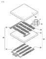
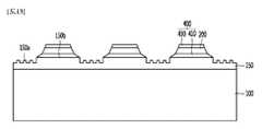
図1ないし図6は、第1実施例によるタッチウィンドウを図示した図である。 1 to 6 illustrate a touch window according to a first embodiment.
図1を参照すると、第1実施例によるタッチウィンドウは、カバー基板(100)、基板(110)、感知電極(200)および配線電極(300)を含むことができる。 Referring to FIG. 1, the touch window according to the first embodiment may include a
前記カバー基板(100)は、リジッド(rigid)であったりまたは、フレキシブル(Flexible)であり得る。 The
例えば、前記カバー基板(100)は、ガラスまたはプラスチックを含むことができる。 For example, the
詳しくは、前記カバー基板(100)は、ソーダライムガラス(Soda lime glaSS)または、アルミノシリケートガラスなどの化学強化または半強化ガラスを含んだり、ポリイミド(Polyimide、PI)、ポリエチレンテレフタレート(polyethylene terephthalate、PET)、プロピレングリコール(propylene glycol、PPG)ポリカーボネート(PC)等の強化あるいは延性プラスチックを含んだりサファイアを含むことができる。 Specifically, the cover substrate (100) includes soda lime glass (Soda lime gla SS) or chemically strengthened or semi-tempered glass such as aluminosilicate glass, polyimide (Polyimide, PI), polyethylene terephthalate (PET), PET ), Reinforced or ductile plastics such as propylene glycol (PPG) polycarbonate (PC) etc. can also contain sapphire.
また、前記カバー基板(100)は、光等方性フィルムを含むことができる。一例として、前記カバー基板(100)は、COC(Cyclic Olefin Copolymer)、COP(Cyclic Olefin Polymer)、光等方ポリカーボネート(polycarbonate、PC)または光等方ポリメタクリル酸メチル(PMMA)等を含むことができる。 In addition, the
サファイアは、誘電率など電気特性が非常に優れていてタッチ反応速度を画期的に上げることができるだけでなく、ホバーリング(Hovering)等空間タッチを簡単に実現できて表面強度が高いためカバー基板としても適用可能な物質である。ここで、ホバーリングとはディスプレーから若干離れた距離でも座標を認識する技術を意味する。 Sapphire has excellent electrical properties such as dielectric constant and can not only increase the touch reaction speed dramatically, but it can easily realize spatial touch such as hovering and has a high surface strength, so it is a cover substrate Is also applicable as a substance. Here, hovering means a technique for recognizing coordinates even at a distance from the display.
また、前記カバー基板(100)は部分的に曲面を有しかつ曲がり得る。すなわち、カバー基板(100)は部分的には平面を有し、部分的には曲面を有しかつ曲がり得る。詳しくは、前記カバー基板(100)の端部が曲面を有しかつ曲がったりランダム(Random)な曲率を含んだ表面を有して反ったり曲がったりすることができる。 In addition, the
また、前記カバー基板(100)は、柔軟な特性を有するフレキシブル(Flexible)基板であり得る。 Also, the
また、前記カバー基板(100)はカーブド(curved)またはベンディド(bended)基板であり得る。すなわち、前記カバー基板(100)を含むタッチウィンドウもフレキシブル、カーブドまたはベンディド特性を有するように形成され得る。これによって、実施例によるタッチウィンドウは携帯が容易であり、多様なデザインに変更が可能であり得る。 Also, the
前記カバー基板(100)上には感知電極(200)、配線電極(300)および印刷回路基板などが配置され得る。すなわち、前記カバー基板(101)は支持基板であり得る。 A
前記カバー基板(100)には有効領域および非有効領域が定義され得る。 An effective area and an ineffective area may be defined on the
前記有効領域においてはディスプレーが表示され得、前記有効領域の周囲に配置される前記非有効領域においてはディスプレーが表示されないことがある。 A display may be displayed in the effective area, and may not be displayed in the non-effective area disposed around the effective area.
また、前記有効領域および前記非有効領域のうち少なくとも一つの領域においては入力装置(例えば、指、スタイラスなど)の位置を感知することができる。このようなタッチウィンドウに指、スタイラスなどの入力装置が接触すると、入力装置が接触した部分で静電容量の差が発生し、このような差が発生した部分を接触位置として検出することができる。 Also, the position of an input device (eg, a finger, a stylus, etc.) can be sensed in at least one of the active area and the non-active area. When an input device such as a finger or a stylus contacts such a touch window, a difference in capacitance occurs at a portion where the input device contacts, and a portion where such a difference occurs can be detected as a contact position. .
前記基板(110)は、前記カバー基板(100)上に配置され得る。前記カバー基板(100)と前記基板(110)は接着層などによって接着され得る。前記基板(110)は前記感知電極(200)および前記配線電極(300)を支持することができる。すなわち、前記基板(110)は前記感知電極(200)および前記配線電極(300)を支持する支持基板であり得る。 The
すなわち、前記感知電極(200)、前記配線電極(300)および前記印刷回路基板は基板(110)により支持され、前記基板(110)と前記カバー基板(100)は接着層を通じて貼合せ(接着)ることができる。 That is, the sensing electrode (200), the wiring electrode (300), and the printed circuit board are supported by a substrate (110), and the substrate (110) and the cover substrate (100) are bonded (bonded) through an adhesive layer. Can be
前記基板(110)は、前述した前記カバー基板(100)と同一または、類似の物質を含むことができる。また、前記基板(110)は前記カバー基板(100)のように曲がることができ、フレキシブル基板を含むことができる。また、前記基板(110)はカーブド(curved)またはベンディド(bended)基板であり得る。 The
前記感知電極(200)は、前記基板(110)上に配置され得る。詳しくは、前記感知電極(200)は前記基板(110)の有効領域および前記非有効領域のうち少なくとも一つの領域に配置され得る。例えば、前記感知電極(200)は前記基板の有効領域上に配置され得る。 The
前記感知電極(200)は、第1感知電極(210)および第2感知電極(220)を含むことができる。 The
前記第1感知電極(210)および前記第2感知電極(220)は前記基板(110)の一面および他面のうち少なくとも一つの面上に配置され得る。詳しくは、前記第1感知電極(210)および前記第2感知電極(220)は前記基板(110)の一面および他面上にそれぞれ配置され得る。すなわち、前記第1感知電極(210)は基板の一面上に配置されて、前記第2感知電極(220)は前記一面と反対となる基板の他面上に配置され得る。 The
前記第1感知電極(210)と前記第2感知電極(220)は互い異なる方向に延長され得る。例えば、前記第1感知電極(210)は一方向に延長され、前記第2感知電極(220)は前記一方向と異なる方向に延長され得る。 The
前記第1感知電極(210)および前記第2感知電極(220)のうち少なくとも一つの感知電極は光の透過を妨害せずに電気が流れるように透明伝導性物質を含むことができる。 At least one sensing electrode of the
一例として、前記感知電極(200)は、インジウムスズ酸化物(indium tin oxide)、インジウム亜鉛酸化物(indium zinc oxide)、銅酸化物(copper oxide)、スズ酸化物(tin oxide)、亜鉛酸化物(zinc oxide)、チタニウム酸化物(titanium oxide)等の金属酸化物を含むことができる。 For example, the
または、前記第1感知電極(210)および前記第2感知電極(220)のうち少なくとも一つの感知電極はナノワイヤー、感光性ナノワイヤーフィルム、炭素ナノチューブ(CNT)、グラフェン(graphene)、伝導性ポリマーまたは、これらの混合物を含むことができる。 Alternatively, at least one of the
ナノワイヤーまたは、炭素ナノチューブ(CNT)のようなナノ合成体を使用する場合、黒色で構成することもでき、ナノパウダーの含有量制御を通じて電気伝導度を確保しながら色と反射率の制御が可能な長所がある。 When using nano wires or nano composites such as carbon nanotubes (CNTs), they can be black, and control of color and reflectance can be achieved while securing electrical conductivity through control of nano powder content There are good points.
または、前記第1感知電極(210)および前記第2感知電極(220)のうち少なくとも一つの感知電極は多様な金属を含むことができる。例えば、前記感知電極(200)はクロム(Cr)、ニッケル(Ni)、銅(Cu)、アルミニウム(Al)、銀(Ag)、モリブデン(Mo)、金(Au)、チタニウム(Ti)およびこれらの合金のうち少なくとも一つの金属を含むことができる。 Alternatively, at least one sensing electrode of the
一例として、前記第1感知電極(210)および前記第2感知電極(220)は金属を含むことができる。 As an example, the
また、前記感知電極(200)はメッシュ形状に形成され得る。詳しくは、感知電極(200)は複数個のサブ電極を含むことができ、前記サブ電極はメッシュ形状に互いに交差しながら配置され得る。 Also, the
例えば、前記第1感知電極(210)および前記第2感知電極(220)のうち少なくとも一つの感知電極はメッシュ形状に形成され得る。詳しくは、前記基板(100)の一面の上に配置される前記第1感知電極(210)および/または、前記基板(100)の他面の上に配置される前記第2感知電極(220)はメッシュ形状に形成され得る。 For example, at least one sensing electrode of the
例えば、前記第1感知電極(210)はメッシュ形状に配置され、前記第2感知電極(220)はバー(bar)形状に配置され得る。しかし、実施例はこれに制限されず、前記第1感知電極(210)および前記第2感知電極(220)いずれもメッシュ形状に形成されたり、または、前記第1感知電極(210)および前記第2感知電極(220)いずれもバー(bar)形状に形成され得ることはもちろんである。 For example, the
詳しくは、前記感知電極はメッシュ形状に互いに交差する複数個のサブ電極によってメッシュ線(LA)および前記メッシュ線(LA)の間のメッシュ開口部(OA)を含むことができる。 Specifically, the sensing electrode may include mesh openings (OA) between mesh lines (LA) and the mesh lines (LA) by a plurality of sub-electrodes crossing each other in a mesh shape.
前記メッシュ線は(LA)の線幅は約0.1umないし約10umであり得る。前記メッシュ線は(LA)の線幅が約0.1um未満であるメッシュ線部は製造工程上不可能であったり、メッシュ線の短絡が発生する可能性があり、約10umを超過する場合、電極パターンが外部で視認されて視認性が低下することがある。望ましくは、前記メッシュ線は(LA)の線幅は約0.5umないし約7umであり得る。さらに望ましくは、前記メッシュ線の線幅は約1umないし約3.5umであり得る。 The mesh line may have a line width of about 0.1 um to about 10 um. The mesh line portion where the line width of (LA) is less than about 0.1 um may not be possible in the manufacturing process, or a short circuit of the mesh line may occur, and if it exceeds about 10 um, An electrode pattern may be visually recognized by the exterior and visibility may fall. Desirably, the mesh line width of (LA) may be about 0.5 um to about 7 um. More preferably, the line width of the mesh line may be about 1 um to about 3.5 um.
また、前記メッシュ開口部(OA)は多様な形状に形成され得る。例えば、前記メッシュ開口部(OA)は四角形、ダイヤモンド型、五角形、六角形の多角形形状または、円形形状など多様な形状を有することができる。また、前記メッシュ開口部は規則的な(regular)形状または、ランダム(random)な形状に形成され得る。 Also, the mesh openings (OA) may be formed in various shapes. For example, the mesh opening (OA) may have various shapes such as a square, a diamond, a pentagon, a hexagonal polygon, or a circular shape. Also, the mesh openings may be formed in a regular shape or a random shape.
前記感知電極がメッシュ形状を有することによって、有効領域の一例として、ディスプレー領域上で前記感知電極のパターンが見えないようにすることができる。すなわち、前記感知電極が金属で形成されても、パターンが見えないようにすることができる。また、前記感知電極が大型の大きさのタッチウィンドウに適用されてもタッチウィンドウの抵抗を低くすることができる。 As the sensing electrode has a mesh shape, the pattern of the sensing electrode can be invisible on the display area as an example of the effective area. That is, even if the sensing electrode is formed of metal, the pattern may not be visible. Also, even if the sensing electrode is applied to a touch window with a large size, the resistance of the touch window can be lowered.
前記配線電極(300)は前記基板(110)上に配置され得る。詳しくは、前記配線電極(300)は前記基板(110)上で前記感知電極(200)と連結されて配置され得る。 The
前記配線電極(300)は前記基板(110)の有効領域および非有効領域のうち少なくとも一つの領域上に配置され得る。例えば、前記配線電極(300)は前記基板(100)の非有効領域上に配置され得る。 The
前記配線電極(300)は第1配線電極(310)および第2配線電極(320)を含むことができる。例えば、前記配線電極(300)は前記第1感知電極(210)と連結される第1配線電極(310)および前記第2感知電極(220)と連結される第2配線電極(320)を含むことができる。 The
前記第1配線電極(310)および前記第2配線電極(320)の一端は前記感知電極(200)と連結され、他端は印刷回路基板と連結され得る。 One end of the
前記配線電極(300)は伝導性物質を含むことができる。一例として、前記配線電極(300)は前述した前記感知電極(200)と同一または、類似の物質を含むことができる。 The
また、前記配線電極(300)は前述した前記感知電極(200)のようにメッシュ形状に形成され得る。 Also, the
図2ないし図6は、第1実施例によるタッチウィンドウの感知電極の一断面を図示した図である。図2ないし図6は感知電極について図示したが、以下の説明は配線電極を含めることはもちろんである。 2 to 6 illustrate one cross section of the sensing electrode of the touch window according to the first embodiment. Although FIGS. 2 to 6 illustrate the sensing electrode, the following description naturally includes the wiring electrode.
図2ないし図6を参照すると、前記基板(110)の一面および他面のうち少なくとも一つの面上には感知電極(200)が配置され得る。前記感知電極(200)は第1感知電極(210)および第2感知電極(220)を含むことができる。 Referring to FIGS. 2 to 6, sensing
図2を参照すると、基板(110)の一面および他面の上に感知電極がそれぞれ配置され得る。 Referring to FIG. 2, sense electrodes may be disposed on one side and the other side of the
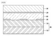
前記感知電極上には反射防止層(400)が配置され得る。 An
前記反射防止層(400)は前記第1感知電極(210)および前記第2感知電極(220)の全面上に配置され得る。例えば、前記反射防止層(400)は前記第1感知電極(210)および前記第2感知電極(220)の少なくとも二面上に配置され得る。例えば、前記反射防止層(400)は前記第1感知電極(210)および前記第2感知電極(220)の四面上に配置され得る。詳しくは、前記反射防止層(400)は前記感知電極の上面、下面および前記上面および下面を連結する側面上に配置され得る。すなわち、前記反射防止層(400)は前記感知電極(200)の全面を囲みながら配置され得る。 The
図2を参照すると、前記反射防止層(400)は第1サブ反射防止層(410)、第2サブ反射防止層(420)および第3サブ反射防止層(430)を含むことができる。 Referring to FIG. 2, the
前記第1サブ反射防止層(410)は前記感知電極(200)および前記基板(100)と接触して配置され得る。例えば、前記第1サブ反射防止層(410)は前記感知電極(200)の一面および前記基板(100)の一面と接触して配置され得る。詳しくは、前記第1サブ反射防止層(410)は前記感知電極(200)と前記基板(100)との間に配置され得る。 The first sub antireflective layer (410) may be disposed in contact with the sensing electrode (200) and the substrate (100). For example, the first
前記第2サブ反射防止層(420)は前記感知電極(200)と接触して配置され得る。例えば、前記第2サブ反射防止層(420)は感知電極(200)の側面と接触して配置され得る。 The second sub antireflective layer (420) may be disposed in contact with the sensing electrode (200). For example, the second sub antireflective layer (420) may be disposed in contact with the side of the sensing electrode (200).
前記第3サブ反射防止層(430)は前記感知電極(200)と接触して配置され得る。例えば、前記第3サブ反射防止層(430)は前記感知電極(200)の前記一面と反対になる他面と接触して配置され得る。 The third
これによって、前記第1サブ反射防止層(410)、前記第2サブ反射防止層(420)および前記第3サブ反射防止層(430)は互いに連結され、前記感知電極(200)上に配置され得る。詳しくは、前記第2サブ反射防止層(420)は前記感知電極(200)の一面上に配置される前記第1サブ反射防止層(410)および前記一面と向き合う他面上に配置される前記第3サブ反射防止層(430)を連結することができる。 Thereby, the first sub antireflective layer (410), the second sub antireflective layer (420) and the third sub antireflective layer (430) are connected to each other and disposed on the sensing electrode (200). obtain. Specifically, the second sub antireflective layer (420) is disposed on the first sub antireflective layer (410) disposed on one surface of the sensing electrode (200) and the other surface facing the one surface. A third sub antireflective layer (430) can be coupled.
すなわち、前記感知電極(200)の一面、他面、および側面すなわち、全面上にはそれぞれ前記第1サブ反射防止層(410)、前記第2サブ反射防止層(420)および前記第3サブ反射防止層(430)が配置され得る。 That is, the first
また、前記第1サブ反射防止層(410)、前記第2サブ反射防止層(420)および前記第3サブ反射防止層(430)は互いに連結されて配置され得る。例えば、前記第1サブ反射防止層(410)、前記第2サブ反射防止層(420)および前記第3サブ反射防止層(430)は一体に形成され得る。 Also, the first sub antireflective layer (410), the second sub antireflective layer (420), and the third sub antireflective layer (430) may be connected to each other. For example, the first
これによって、前記第1サブ反射防止層(410)、前記第2サブ反射防止層(420)および前記第3サブ反射防止層(430)は前記感知電極(200)の全面を囲みながら配置され得る。 Accordingly, the first sub antireflective layer (410), the second sub antireflective layer (420) and the third sub antireflective layer (430) may be disposed to surround the entire surface of the sensing electrode (200). .
第1実施例によるタッチウィンドウは前記感知電極(200)の全面に反射防止層(400)が配置されるため、前記感知電極(200)が外部から酸化または、腐食することを防止することができる。すなわち、前記反射防止層が前記感知電極上に配置されて保護層の役割をして、外部の不純物などから前記感知電極を保護することができる。これによって、第1実施例によるタッチウィンドウの信頼性を向上させることができる。 The
また、前記感知電極(200)は異種物質である前記基板(110)上に直接接触せずに前記反射防止層(400)上に配置されるため、感知電極(200)が前記基板(110)から剥離することを防止することができる。すなわち、前記反射防止層(400)は前記基板(110)と前記感知電極(200)との間でバッファー層の役割をするため、前記感知電極(200)と前記基板(110)との密着力を向上させることができる。これによって、第1実施例によるタッチウィンドウの信頼性を向上させることができる。 In addition, since the
例えば、前記基板(110)の一面および他面上に配置される前記第1感知電極(210)および前記第2感知電極(220)は一体に形成され得る。 For example, the
例えば、前記第1感知電極(210)および前記第2感知電極(220)はめっき層であり得る。例えば、前記第1感知電極(210)および前記第2感知電極(220)は無電解めっきを通じて前記基板(110)上に一体に配置され得る。ここで、無電解めっきとは外部から水溶液に電気エネルギーを与えずに行うめっきをいう。詳しくは、前記第1感知電極(210)および前記第2感知電極(220)は湿式工程を通じて同時に形成され得る。これによって、第1実施例によるタッチウィンドウは工程効率を向上させることができる。 For example, the
また、前記感知電極(200)は無電解めっきを通じて薄い厚さに配置され得る。これによって、第1実施例によるタッチウィンドウの全体的な厚さを減少させることができる。 Also, the
前記感知電極(200)の厚さ(T1)は約200nmないし約900nmであり得る。例えば、前記感知電極(200)の厚さ(T1)は約200nmないし約700nmであり得る。例えば、前記感知電極(200)の厚さ(T1)は約200nmないし約500nmであり得る。 The thickness T1 of the
例えば、前記感知電極(200)の厚さ(T1)が約200nm未満で形成される場合には電極の抵抗が大きくなって信頼性が低下することがある。また、前記感知電極(200)の厚さ(T1)が約900nmを超過して形成される場合にはタッチウィンドウの全体的な厚さが増加することがあり、工程効率が低下することがある。 For example, if the thickness T1 of the
また、前記感知電極(200)は無電解めっきを通じて均一な厚さで前記基板(110)上に配置され得る。例えば、前記第1感知電極(210)の厚さ(T1)は前記第2感知電極(220)の厚さ(T2)と対応し得る。これによって、第1実施例によるタッチウィンドウの信頼性を向上させることができる。 Also, the
前記反射防止層(400)の厚さは前記感知電極(200)の厚さと互いに異なることがある。例えば、前記感知電極(200)の厚さは前記反射防止層(400)の厚さより大きいことがある。 The thickness of the
例えば、前記感知電極(200)の厚さに対する前記反射防止層(400)の厚さは約25:1以下であり得る。例えば、前記感知電極(200)の厚さと前記反射防止層(400)の厚さは約18:1ないし約25:1であり得る。例えば、前記感知電極(200)の厚さと前記反射防止層(400)の厚さは約18:1ないし約20:1であり得る。前記感知電極(200)の厚さに対する前記反射防止層(400)の厚さが約25:1を超過する場合には感知電極が視認され得、感知電極と基板との間の密着力が低下することがある。 For example, the thickness of the
また、前記反射防止層(400)は均一な厚さで前記感知電極(200)上に配置され得る。例えば、前記第1サブ反射防止層(410)の厚さ(D1)、前記第2サブ反射防止層(420)の厚さ(D2、D3)および前記第3サブ反射防止層(430)の厚さ(D4)は互いに対応し得る。これによって、第1実施例によるタッチウィンドウの信頼性を向上させることができる。 Also, the
前記反射防止層(400)の厚さ(D)は10nmないし50nmであり得る。例えば、前記反射防止層(400)の厚さ(D)は10nmないし30nmであり得る。例えば、前記反射防止層(400)の厚さ(D)は10nmないし20nmであり得る。 The thickness (D) of the
前記反射防止層(400)の厚さ(D)が約10nm未満に形成される場合には前記感知電極(200)が視認され得る。 The
また、前記反射防止層(400)の厚さ(D)が約50nmを超過して形成される場合にはタッチウィンドウの全体的な厚さが増加し得、工程効率が低下することがある。 In addition, if the thickness (D) of the
この時、前記反射防止層(400)の厚さ(D)は前記第1サブ反射防止層(410)の厚さ(D1)、前記第2サブ反射防止層(420)の厚さ(D2、D3)および前記第3サブ反射防止層(430)の厚さ(D4)の平均厚さを意味することがある。 At this time, the thickness D of the
前記感知電極(200)は前記反射防止層(400)と互いに対応する物質を含むことができる。例えば、前記感知電極(200)は前記反射防止層(400)と対応する金属を含むことができる。例えば、前記反射防止層(400)は金属酸化物を含むことができる。詳しくは、前記感知電極(200)は金属を含み、前記反射防止層(400)は前記金属を含む酸化物すなわち、金属酸化物を含むことができる。さらに詳しくは、前記感知電極(200)は第1金属を含み、前記反射防止層(400)は前記第1金属を含む酸化物すなわち、第1金属酸化物を含むことができる。 The
しかし、実施例はこれに制限されず、前記感知電極(200)は前記反射防止層(400)と互いに異なる物質を含むことができる。前記反射防止層(400)は合金を含むことができる。例えば、前記反射防止層(400)はCu2Se、Cu−PDのうち少なくとも一つの化合物を含むことができる。例えば、前記感知電極(200)は前記反射防止層(400)と別に形成され得る。However, embodiments are not limited thereto, and the
前記反射防止層(400)は一定の色を有することができる。 The
前記反射防止層(400)の明度指数(L*)は約40以下であり得る。例えば、前記反射防止層(400)の明度指数(L*)は約0ないし約40であり得る。例えば、前記反射防止層(400)の明度指数(L*)は約10ないし約40であり得る。前記反射防止層(400)の明度指数(L*)が約40以下である時、前記感知電極(200)が外部で視認されることを防止することができる。前記明度指数(L*)は明度を示す数値であって、100に近づくほど白色を示し、0に近づくほど黒色を示す指数を意味する。The lightness index (L* ) of the
前記反射防止層(400)の色度指数(b*)は負の値を有することができる。例えば、前記反射防止層(400)の色度指数(b*)は−10以下であり得る。例えば、前記反射防止層(400)の色度指数(b*)は−15以下であり得る。前記反射防止部(400)の色度指数(b*)が負の値を有する時、前記感知電極(200)が外部で視認されることを防止することができる。前記色度指数(b*)は色座標単位の一つであって、前記色度指数が負の値を有する場合、青色(blue)の色を有することができ、正の値を有する場合、黄色(yellow)の値を有することができる。また、色度指数の大きさにより青色または、黄色の色が濃くなり得る。The chromaticity index b* of the
例えば、前記反射防止層(400)は黒色系列の色を有することができる。詳しくは、前記反射防止層(400)は黒色(black)、灰色(gray)およびこれらの混合色のうち少なくとも一つの色を含むことができる。 For example, the
例えば、前記反射防止層(400)は黒化物質で形成され得る。黒化物質は黒色の金属酸化物であり得る。例えば、CuO、CrO、FeO、Ni2O3のうち選択されるいずれか一つを適用できるが、これに限定されることではなく、前記感知電極(200)の反射性を抑制することができる黒色系統の物質を適用することができる。For example, the
すなわち、前記反射防止層(400)は感知電極(200)の反射を防止することができる。詳しくは、感知電極(200)の上面、下面および側面が輝くことによって視認されることを防止することができる。 That is, the
例えば、前記反射防止層(400)は感知電極のように、湿式工程を通じて形成され得る。これによって、工程効率が向上され得る。 For example, the
図2においては前記感知電極(200)が四角形の形状に配置されることを図示したが、実施例はこれに制限されず、前記感知電極(200)が傾斜を有したり曲面形状であるものを含むことができる。 Although FIG. 2 illustrates that the
図3を参照すると、前記感知電極(200)は傾斜面を含むことができる。例えば、前記感知電極(200)と前記基板(100)が接触する一面で前記一面と反対となる他面に延長するほど前記感知電極(200)の幅が狭くなるように傾斜面を含むことができる。詳しくは、前記傾斜面は直線または、直線に近い形状であり得る。 Referring to FIG. 3, the
また、前記反射防止層(400)は前記感知電極(200)の全面上に配置され得る。すなわち、前記第1サブ反射防止層(410)、前記第2サブ反射防止層(420)および前記第3サブ反射防止層(430)は傾斜面を含む感知電極(200)の全面上に配置され得る。これによって、前記第2サブ反射防止層(420)は前記基板(110)と鋭角の角度に傾斜して前記第1サブ反射防止層(410)および前記第3サブ防止層(430)を連結することができる。 Also, the
図4を参照すると、前記感知電極(200)は曲面を含むことができる。例えば、前記感知電極(200)は前記感知電極(200)と前記基板(110)が接触する一面および前記一面と反対となる他面を含み、前記他面は曲面を含むことができる。 Referring to FIG. 4, the
また、前記反射防止層(400)は前記感知電極(200)の全面上に配置され得る。すなわち、前記第1サブ反射防止層(410)は前記基板(110)と前記感知電極(200)の一面との間に配置され得、前記第3サブ反射防止層(430)は曲面を有しながら前記感知電極(200)の他面上に配置され得る。前記第1サブ反射防止層(410)は前記第3サブ反射防止層(430)と連結され得る。 Also, the
図2ないし図4では基板上に感知電極(210)が配置されることを図示したが、実施例はこれに制限されず、前記感知電極(210)はパターン部の内部に配置され得る。 Although FIGS. 2 to 4 illustrate that the
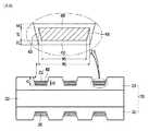
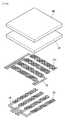
図5および図6を参照すると、前記基板(100)上には基材(150)がさらに配置され得る。例えば、前記基板(100)の一面または他面上に基材(150)が配置され得、前記基材(150)上には複数個の陰刻パターン部(P)が形成され得る。前記パターン部(P)は全体的にメッシュ形状に形成され得る。 Referring to FIGS. 5 and 6, a substrate (150) may be further disposed on the substrate (100). For example, a
前記基材(150)は光硬化性樹脂(UV樹脂)または、熱硬化性樹脂などを含むことができるが、実施例はこれに制限されない。また、前記基材(150)の陰刻パターンは前記陰刻パターンと相補的な形状を有する陽刻パターンのモールドをインプリンティングすることによって形成され得る。 The
図5を参照すると、前記基材(150)の陰刻パターン部(P)内に感知電極(200)および前記感知電極(200)の全面を囲みながら配置される反射防止層(400)が配置され得る。 Referring to FIG. 5, a
実施例による感知電極は基板(100)上に光硬化性樹脂(UV樹脂)または、熱硬化性樹脂を含む基材(150)を形成した後、前記基材上にメッシュ形状の陰刻パターンを形成した後、前記陰刻パターン内に伝導性物質を充填して形成され得る。この時、前記基材(150)の陰刻パターンは陽刻パターンを有するモールドをインプリンティングすることによって形成され得る。 The sensing electrode according to the embodiment forms a photocurable resin (UV resin) or a substrate (150) including a thermosetting resin on a substrate (100) and then forms a mesh-shaped intaglio pattern on the substrate Then, the intaglio pattern may be filled with a conductive material. At this time, the intaglio pattern of the
図6を参照すると、前記基板(100)上には互いに異なる大きさを有するパターンが形成された基材(150)が配置され得る。 Referring to FIG. 6, substrates (150) having patterns of different sizes may be disposed on the substrate (100).
前記基材(150)は第1パターン(150a)および第2パターン(150b)を含むことができる。詳しくは、前記基材(150)は互いに異なる幅を有する第1パターン(150a)および第2パターン(150b)を含むことができる。また、前記第1パターン(150a)および前記第2パターン(150a)は陽刻パターンであり得る。また、前記第1パターン(150a)は数ナノメートル(nm)の幅を有することができ、前記第2パターン(150b)は数マイクロメーター(um)の幅を有することができる。すなわち、前記第2パターン(150b)の幅が前記第1パターン(150a)の幅よりさらに大きいことがある。 The
前記第1パターン(150a)および前記第2パターン(150b)は陽刻パターンと相補的な形状を有する陰刻パターンを含むモールドをインプリンティングすることによって形成され得る。 The
前記感知電極(200)および前記反射防止層(400)は前記第2パターン(150b)上に配置され得る。 The
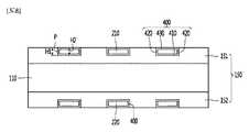
以下、図7ないし図9を参照し、第2実施例によるタッチウィンドウについて説明する。前述した第1実施例と重複する説明は省略され得る。同一の構成に対しては同一の図面符号を付与する。 Hereinafter, a touch window according to a second embodiment will be described with reference to FIGS. 7 to 9. The description overlapping with the first embodiment described above may be omitted. The same reference numerals are assigned to the same components.
図7を参照すると、第2実施例によるタッチウィンドウは、前記基板(110)の一面および他面すなわち、前記基板(110)の両面上にそれぞれ前記第1感知電極(210)および前記第2感知電極(220)が配置され得る。これによって、一つの基板(110)上に前記第1感知電極(210)および前記第2感知電極(220)がすべて配置され得るため、タッチウィンドウの全体的な厚さを減少させることができる。 Referring to FIG. 7, the touch window according to the second embodiment includes the
すなわち、実施例によるタッチウィンドウは別途の基板上にそれぞれ感知電極(210)を配置する場合に比べ、接着層および一つの基板を省略することができるためタッチウィンドウの全体的な厚さを減少させることができる。 That is, the touch window according to the embodiment reduces the overall thickness of the touch window because the adhesive layer and one substrate can be omitted as compared to the case where the
前記基板(110)の両面すなわち、前記基板(110)の一面上に配置される前記第1感知電極(210)および/または、前記基板(110)の他面上に配置される前記第2感知電極(220)はメッシュ形状に形成され得る。 The first sensing electrode (210) disposed on both sides of the substrate (110), ie, one side of the substrate (110) and / or the second sensing disposed on the other side of the substrate (110) The
前記メッシュ線(LA)の線幅は約0.1umないし約10umであり得る。望ましくは、前記メッシュ線は(LA)の線幅は約0.5umないし約7umであり得る。さらに望ましくは、前記メッシュ線の線幅は約1umないし約3.5umであり得る。 The line width of the mesh lines LA may be about 0.1 um to about 10 um. Desirably, the mesh line width of (LA) may be about 0.5 um to about 7 um. More preferably, the line width of the mesh line may be about 1 um to about 3.5 um.
また、前記メッシュ線(LA)の厚さは約100nmないし約500nmであり得る。前記メッシュ線(LA)の厚さが約100nm未満である場合、電極抵抗が高まって電気的特性が低下することがあり、約500nmを超過する場合、タッチウィンドウの全体的な厚さが厚くなり、工程効率が低下することがある。望ましくは、前記メッシュ線(LA)の厚さは約150nmないし約200nmであり得る。さらに望ましくは、前記メッシュ線(LA)の厚さは約180nmないし約200nmであり得る。 Also, the thickness of the mesh line LA may be about 100 nm to about 500 nm. When the thickness of the mesh line (LA) is less than about 100 nm, the electrode resistance may be increased and the electrical characteristics may be decreased, and when it exceeds about 500 nm, the overall thickness of the touch window may be increased. Process efficiency may be reduced. Desirably, the thickness of the mesh line (LA) may be about 150 nm to about 200 nm. More preferably, the mesh line (LA) may have a thickness of about 180 nm to about 200 nm.
図面には図示されなかったが、前記基板の非有効領域上にはテコ層が配置され得る。前記テコ層は前記基板の非有効領域上に配置され、前記配線電極および前記配線電極を外部回路に連結する印刷回路基板などを外部で視認されないように所定の色を有する物質を塗布して形成することができる。 Although not shown in the drawings, a leverage layer may be disposed on the non-effective area of the substrate. The lever layer is formed on a non-effective area of the substrate by applying a material having a predetermined color so that a printed circuit board or the like connecting the wiring electrode and the wiring electrode to an external circuit is not visually recognized. can do.
前記テコ層は所望の外観に適合した色を有することができるが、一例として黒色または、白色顔料などを含んで黒色または、白色を示すことができる。または、多様なカラーフィルムなどを使用して赤色、青色などの多様なカラー色を示すことができる。 The lever layer can have a color adapted to the desired appearance, but as an example, it can be black or white, including a white pigment or the like. Alternatively, various color films can be used to show various colors such as red and blue.
前記テコ層をフィルムで配置する場合、曲面または、フレキシブルな基板にテコ層を配置するとき容易に配置することができる。 When arranging the lever layer with a film, it can be easily arranged when arranging the lever layer on a curved or flexible substrate.
そしてこのテコ層には多様な方法で所望のロゴなどを形成することができる。このようなテコ層は蒸着、印刷、湿式コーティングなどによって形成され得る。 And a desired logo etc. can be formed on this lever layer by various methods. Such a leverage layer may be formed by vapor deposition, printing, wet coating and the like.
前記テコ層は少なくとも1層以上で配置され得る。例えば、前記テコ層は一つの層に配置されたりまたは、幅が互いに異なる少なくとも二層で配置され得る。 The lever layer may be disposed in at least one or more layers. For example, the lever layer may be disposed in one layer or in at least two layers having different widths.
前記テコ層は前記基板の一面および他面のうち少なくとも一つの面上に配置され得る。 The leverage layer may be disposed on at least one of the one side and the other side of the substrate.
図8を参照すると、第2実施例によるタッチウィンドウは基板(110)上の基材(150)および前記基材(150)上の前記感知電極(200)を含むことができる。 Referring to FIG. 8, the touch window according to the second embodiment may include a
前記基材(150)はプラスチックを含むことができる。例えば、前記基材(150)は樹脂(resin)を含むことができる。一例として、前記基材(150)はUV樹脂などの光硬化性樹脂または、熱硬化性樹脂などを含むことができる。 The substrate (150) may comprise plastic. For example, the
前記基材(150)はパターン部(P)を含むことができる。 The
例えば、前記基材(150)の一面および他面上には陰刻のパターン部(P)が形成され得る。前記パターン部(P)はメッシュ形状に形成され得る。詳しくは、前記パターン部(P)は互いに交差するメッシュ形状に形成され得る。 For example, an intaglio pattern portion (P) may be formed on one surface and the other surface of the substrate (150). The pattern part P may be formed in a mesh shape. In detail, the pattern part (P) may be formed in a mesh shape crossing each other.
前記感知電極(200)は前記基材(150)上に配置され得る。例えば、前記感知電極(200)は前記パターン部(P)内に配置され得る。これによって、前記感知電極(200)は前記基材(150)上でメッシュ形状に配置され得る。 The sensing electrode (200) may be disposed on the substrate (150). For example, the
例えば、前記基板(110)の一面上に第1基材(151)が配置され、前記第1基材(151)のパターン部(P)内に前記第1感知電極(210)が配置され、前記基板(110)の他面上に第2基材(152)が配置され、前記第2基材(152)のパターン部(P)内に前記第2感知電極(220)が配置され得る。 For example, a
前記感知電極は前述した伝導性物質を含むことができる。例えば、前記感知電極は前記伝導性物質を含む伝導性ペーストを前記パターン部に充填して形成され得る。 The sensing electrode may include the conductive material described above. For example, the sensing electrode may be formed by filling a conductive paste containing the conductive material in the pattern part.
前記伝導性ペーストは伝導性粉末、溶媒およびバインダーなどを混合して形成され得る。 The conductive paste may be formed by mixing conductive powder, solvent, binder and the like.
前記伝導性粉末は前述した金属を含むことができる。すなわち、前記伝導性粉末はクロム(Cr)、ニッケル(Ni)、銅(Cu)、アルミニウム(Al)、銀(Ag)、モリブデン(Mo)、金(Au)、チタニウム(Ti)およびこれらの合金のうち少なくとも一つの金属を含む金属粉末であり得る。 The conductive powder can include the metals described above. That is, the conductive powder includes chromium (Cr), nickel (Ni), copper (Cu), aluminum (Al), silver (Ag), molybdenum (Mo), gold (Au), titanium (Ti) and alloys thereof And at least one metal.
前記バインダーは前記金属粉末と基板との間に接着力を付与する役割をすることができる。一例として、前記バインダーは、エポキシ系(epoxy)、エステル系(ester)、アクリル系(acryl)およびビニール類(vinyl)から成る群の少なくとも一つを含み得るが、これに限定される訳ではない。 The binder may serve to provide adhesion between the metal powder and the substrate. As one example, the binder may include, but is not limited to, at least one of the group consisting of epoxy, ester, acrylic and vinyl. .
また、前記溶媒は前記バインダーを溶解できる有機溶媒を含むことができる。一例として、前記溶媒はアルコール類(alcohols)、グリコール類(glycols)、ポリオール類(polyols)、エーテル類(ethers)、グリコールエーテル類(glycol ethers)、グリコールエーテルエステル類(glycol ether esters)およびエステル類から成る群から少なくとも一つを含むことができるが、これに限定されるものではない。 Also, the solvent may include an organic solvent capable of dissolving the binder. As an example, the solvent may be alcohols (alcohols), glycols (glycols), polyols (polyols), ethers (ethers), glycol ethers (glycol ethers), glycol ether esters (esters) and esters And at least one of the group consisting of, but not limited to.
このような伝導性ペーストを前記基材(150)上に塗布した後、ローリング(rolling)部材を利用し、前記基材のパターン部内に前記伝導性ペーストを充填することができる。 After applying such a conductive paste on the
これによって、前記伝導性ペーストは前記パターン部(P)内に充填され、全体的にメッシュ形状を有する感知電極(200)が形成され得る。 Accordingly, the conductive paste may be filled in the pattern part P to form a
または、前記感知電極(200)は電気めっきまたは、無電解めっき方法によって前記パターン部内に蒸着することができる。前記感知電極(200)を電気めっきまたは、無電解めっき方法で直接蒸着する場合、ペーストに比べて電気的特性が優れた金属を直接前記基材(150)上に蒸着することができる。これによって、前記感知電極(200)は薄い厚さで蒸着することができ、電極の厚さを減少させることができる。 Alternatively, the
また、電気めっきまたは、無電解めっき方法によって蒸着することによって、ペーストを塗布することに比べてパターン部内により均一な厚さで電極を蒸着することができる。これによって、実施例によるタッチウィンドウの信頼性を向上させることができる。 In addition, by depositing by electroplating or electroless plating, it is possible to deposit an electrode with a more uniform thickness in the pattern portion as compared to applying a paste. This can improve the reliability of the touch window according to the embodiment.
前記反射防止層(400)は前記感知電極(200)上に配置され得る。例えば、前記反射防止層(400)は前記第1感知電極(210)および前記第2感知電極(220)上にそれぞれ配置され得る。 The antireflective layer (400) may be disposed on the sensing electrode (200). For example, the
前記反射防止層(400)は前記感知電極(200)と接触して配置され得る。例えば、前記反射防止層(400)は前記感知電極(200)と直接接触して配置され得る。 The
前記反射防止層(400)は前記感知電極(200)の全面上に配置され得る。例えば、前記感知電極(200)が上面、下面、左側面および右側面を含む場合、前記反射防止層(400)は前記感知電極(200)の上面、下面、左側面および右側面の全体の面上に配置され得る。 The
すなわち、前記感知電極(200)は前記反射防止層(400)で囲みながら配置され得る。これによって、前記感知電極(200)および前記感知電極を囲みながら配置される前記反射防止層(400)は前記パターン部(P)内に配置され得る。 That is, the
前記反射防止層(400)は前記感知電極(200)の下面上に配置される第1サブ反射防止層(410)、前記感知電極(200)の両側面上に配置される第2サブ反射防止層(420)および前記感知電極(200)の上面上に配置される第3サブ反射防止層(430)を含むことができる。 The
前記第1サブ反射防止層(410)、前記第2サブ反射防止層(420)および前記第3サブ反射防止層(430)は一体に形成され得る。 The first
また、前記第1サブ反射防止層(410)、前記第2サブ反射防止層(420)および前記第3サブ反射防止層(430)は同時に形成され得る。 Also, the first
または、前記第1サブ反射防止層(410)および前記第2サブ反射防止層(420)が同時に形成され、前記第1サブ反射防止層(410)および前記第2サブ反射防止層(420)上に感知電極(200)が形成された後、前記第3サブ反射防止層(430)が形成され得る。 Alternatively, the first sub antireflective layer (410) and the second sub antireflective layer (420) are simultaneously formed, and the first sub antireflective layer (410) and the second sub antireflective layer (420) are formed. The third
例えば、前記基板(110)上に配置される前記基材(150)は表面処理を通じて粗?度が増加することができる。前記基材(150)は金属を含む有機溶媒で処理することができる。例えば、前記基材(150)はPdまたはAgを含む有機溶媒で処理することができる。次に、有機溶媒に含まれた金属を還元させることによって、前記第1サブ反射防止層(410)および前記第2サブ反射防止層(420)を形成することができる。この時、前記第1サブ反射防止層(410)および前記第2サブ反射防止層(420)は黒化層であり得る。前記基材(150)は表面の粗?度が増加することによって、PdまたはAgのような金属の付着性が増加することができ、黒化層が優れて形成され得る。次に、前記感知電極(200)が形成され得、前記感知電極(200)上に配置される前記第3サブ反射防止層(430)は前記感知電極(200)の表面を酸化させたり、前記第1サブ反射防止層(410)および前記第2サブ反射防止層(420)の形成方法と同一の方法で処理して形成することができる。 For example, the substrate (150) disposed on the substrate (110) may be roughened through surface treatment? The degree can be increased. The substrate (150) can be treated with a metal-containing organic solvent. For example, the substrate (150) can be treated with an organic solvent comprising Pd or Ag. Next, the first sub antireflective layer (410) and the second sub antireflective layer (420) can be formed by reducing the metal contained in the organic solvent. At this time, the first
また、前記第1サブ反射防止層(410)、前記第2サブ反射防止層(420)および前記第3サブ反射防止層(430)は同一または、類似の物質を含むことができる。すなわち、前記第1サブ反射防止層(410)、前記第2サブ反射防止層(420)および前記第3サブ反射防止層(430)は互いに対応する物質を含むことができる。 In addition, the first
また、前記第1サブ反射防止層(410)、前記第2サブ反射防止層(420)および前記第3サブ反射防止層(430)は互いに同一または、類似の厚さに配置され得る。 In addition, the first
前記反射防止層(400)は電気めっきまたは、無電解めっき方法によって前記感知電極(200)上に配置することができる。前記反射防止層(400)を電気めっきまたは、無電解めっき方法で蒸着する場合、前記パターン部内に反射防止層の厚さを均一に蒸着させることができる。すなわち、前記反射防止層(400)はめっき層であり得る。詳しくは、前記第1サブ反射防止層(410)、前記第2サブ反射防止層(420)および前記第3サブ反射防止層(430)はめっき層であり得る。 The
前記第1サブ反射防止層(410)は前記基材(150)と前記感知電極(200)との間に形成され、前記感知電極(200)と前記基材(120)との密着力を向上させることができる。これによって、前記感知電極(200)の脱膜または、分離を防止し、タッチウィンドウの信頼性を向上させることができる。 The first sub antireflective layer (410) is formed between the substrate (150) and the sensing electrode (200) to improve adhesion between the sensing electrode (200) and the substrate (120). It can be done. Thus, it is possible to prevent film removal or separation of the
また、前記反射防止層(400)は前記感知電極(200)上に配置され、前記感知電極(200)の保護層の役割をすることができる。例えば、前記反射防止層(400)は前記感知電極(200)の上面、下面または、両側面が外部に露出されて酸化または、腐食することを防止することができ、タッチウィンドウの信頼性を向上させることができる。 In addition, the
前記反射防止層(400)は前記パターン部(P)内に配置されるため、前記第3サブ反射防止層(430)の幅は前記第1サブ反射防止層(410)の幅と互いに対応し得る。ただし、実施例がこれに制限される訳ではなく、前記パターン部(P)は多様な陰刻パターンで形成され得ることはもちろんである。 Since the
前記反射防止層(400)は金属を含むことができる。詳しくは、前記反射防止層(400)はCu2Se、Pd、AgまたはNbなどの金属を含むことができる。The
例えば、前記反射防止層(400)は金属酸化物を含むことができる。詳しくは、前記反射防止層(400)はCuO、CrO、FeOまたはNi2O3等の金属酸化物を含むことができる。しかし、実施例はこれに限定されず、感知電極の反射性を抑制できる多様な金属または、金属酸化物を含み得ることはもちろんである。For example, the
すなわち、前記反射防止層(400)は前記感知電極(200)上に配置され、前記感知電極(200)の視認性を向上させることができる。例えば、前記第1サブ反射防止層(410)は前記感知電極(200)の下面上に配置され、前記第2サブ反射防止層(420)は前記感知電極(200)の両側面上に配置され、前記第3サブ反射防止層(430)は前記感知電極(200)の上面上に配置されることによって、前記感知電極(200)の上面、下面または、両側面の輝きによる視認性低下を防止することができる。 That is, the
前記反射防止層(400)は色を有することができる。例えば、前記反射防止層(400)は黒色系列の色を含むことができる。詳しくは、前記反射防止層(400)は黒色(black)、灰色(gray)およびこれらの混合色のうち少なくとも一つの色を含むことができる。 The
前記反射防止層(400)および感知電極(200)は同時に形成されたり、別途の工程で形成され得る。 The
前記感知電極(200)の厚さは前記反射防止層の厚さと互いに異なり得る。例えば、前記感知電極(200)の厚さは前記反射防止層の厚さよりさらに大きい厚さで配置され得る。例えば、前記感知電極(200)の厚さより前記反射防止層の厚さがさらに大きい場合には、実施例によるタッチウィンドウの電気的な特性が低下することがある。 The thickness of the
一方、前記第2サブ反射防止層(420)は前記基材(150)のパターン部(P)の側面と対応する傾斜角を有することができる。すなわち、前記第2サブ反射防止層(420)は前記感知電極(200)の下面に配置される前記第1サブ反射防止層(410)と連結される内角が90度であり得、前記感知電極の上面に配置される前記第3サブ反射防止層(430)と連結される内角が90度であり得る。これによって、向き合う前記第2サブ反射防止層(420)は前記感知電極(200)を間に置いて互いに平行するように配置され得る。 Meanwhile, the second
前記パターン部(P)の高さ(H1)は前記パターン部(P)内に配置される前記感知電極(200)および前記反射防止層(400)の高さ(H2)と対応し得る。 The height H1 of the pattern unit P may correspond to the height H2 of the
図9を参照すると、前記基材(150)のパターン部(P)の側面は傾斜面を含むことができる。これによって、前記感知電極(200)の下面と上面の幅は互いに異なり得る。 Referring to FIG. 9, the side surface of the pattern portion (P) of the
例えば、前記感知電極(200)は前記基材(150)と接触する下面から前記下面と反対になる表面に延長するほど幅が広くなり得る。詳しくは、前記感知電極の前記基材と接触する下面の幅(W1)は前記下面と反対になる上面の幅(W2)より小さいことがある。さらに詳しくは、前記感知電極(200)は前記基板方向に延長するほど、すなわち基板との距離が近くなるほど幅が狭くなり得る。 For example, the
すなわち、前記反射防止層(400)は前記パターン部(P)内に配置されるため、前記第3サブ反射防止層(430)の幅は前記第1サブ反射防止層(410)と互いに異なり得る。例えば、前記第3サブ反射防止層(430)の幅は前記第1サブ反射防止層(410)より大きいことがある。これによって、前記感知電極(200)の充填効率を向上させることができ、タッチウィンドウの信頼性を向上させることができる。 That is, since the
一方、前記第2サブ反射防止層(420)は前記基材(150)のパターン部(P)の側面が有する傾斜角と対応する傾斜角を有することができる。すなわち、前記第2サブ反射防止層(420)は前記感知電極(200)の下面に配置される前記第1サブ反射防止層(410)と連結される内角が90度超過の鈍角であり得、前記感知電極の上面に配置される前記第3サブ反射防止層(430)と連結される内角が90度未満の鋭角であり得る。これによって、向き合う前記第2サブ反射防止層(420)は前記感知電極(200)の上面から下面に行くほど互いに離隔した距離が近くなり得る。 Meanwhile, the second
前記感知電極(200)の厚さ(T1)は前記反射防止層の厚さと互いに異なり得る。例えば、前記感知電極(200)の厚さ(T1)は前記反射防止層の厚さよりさらに大きい厚さで配置され得る。詳しくは、前記感知電極(200)の厚さ(T1)は前記第1サブ反射防止層(410)の厚さ(D1)よりさらに大きい厚さで配置され得る。詳しくは、前記感知電極(200)の厚さ(T1)は前記第3サブ反射防止層(430)の厚さ(D4)よりさらに大きい厚さで配置され得る。 The thickness T1 of the
これによって、前記感知電極(200)の電気的特性を確保すると同時に、前記感知電極(200)が視認されることを防止することができる。 Thus, the electrical characteristics of the
前記パターン部(P)の高さ(H1)は前記パターン部(P)内に配置される前記感知電極(200)および前記反射防止層(400)の高さ(H2)より大きいことがある。これによって、前記感知電極(200)の脱膜を防止することができ、前記第3サブ反射防止層(430)の損傷を防止することができ、前記反射防止層(400)による前記感知電極(200)の保護効果を向上させることができる。 The height H1 of the pattern part P may be greater than the height H2 of the
実施例によるタッチウィンドウは基板の一面および他面上に感知電極が配置されるため、タッチウィンドウの厚さが薄くなり得る。また、前記感知電極は反射防止層で囲みながら配置されるため、信頼性および視認性が向上され得る。また、実施例によるタッチウィンドウは基板の一面および他面上に感知電極および前記感知電極を囲む反射防止層が同時に形成されるために工程効率性が向上され得る。 The touch window according to the embodiment may have a thinner touch window because the sensing electrodes are disposed on one and the other sides of the substrate. In addition, since the sensing electrodes are disposed around the antireflective layer, reliability and visibility may be improved. In addition, the touch window according to the embodiment may improve the process efficiency because the sensing electrode and the antireflective layer surrounding the sensing electrode are simultaneously formed on one surface and the other surface of the substrate.
以下、図10ないし図16を参照し、第3実施例によるタッチウィンドウについて説明する。前述した第1実施例と重複する説明は省略され得る。同一の構成に対しては同じ図面符号を付与する。 Hereinafter, the touch window according to the third embodiment will be described with reference to FIGS. 10 to 16. The description overlapping with the first embodiment described above may be omitted. The same reference numerals are assigned to the same components.
図10を参照すると、第3実施例によるタッチウィンドウは、基板(110)上には感知電極(200)、配線電極(300)および印刷回路基板(250)等が配置され得る。すなわち、前記基板(110)は支持基板であり得る。 Referring to FIG. 10, in the touch window according to the third embodiment, a
前記配線電極(300)は前記感知電極(200)と連結され、前記非有効領域(UA)方向に延長され、前記非有効領域(UA)上で印刷回路基板(250)と連結され得る。 The
図11ないし図13は第3実施例によるタッチウィンドウの断面図を図示した図面である。 11 to 13 are cross-sectional views of a touch window according to a third embodiment.
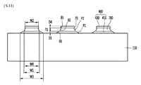
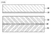
図11を参照すると、前記感知電極(200)上には反射防止層(400)が配置され得る。詳しくは、前記反射防止層(400)は前記感知電極(200)の一面および他面のうち少なくとも一つの面上に配置され得る。さらに詳しくは、前記反射防止層(400)は前記感知電極(200)の一面および他面上に配置され得る。 Referring to FIG. 11, an
図11を参照すると、前記反射防止層(400)は、前記感知電極(200)の一面上に配置される第1反射防止層(410)および前記一面と反対となる他面上に配置される第3反射防止層(430)を含むことができる。 Referring to FIG. 11, the
前記第1反射防止層(410)は前記感知電極(200)の一面と直接または、間接的に接触しながら配置され得る。また、前記第3反射防止層(430)は前記感知電極(200)の他面と直接または、間接的に接触しながら配置され得る。 The
これによって、前記基板(110)上には前記第1反射防止層(410)、前記感知電極(200)および前記第3反射防止層(430)が順次に配置され得る。 Thus, the first
一方、前記感知電極(200)は前記反射防止層(400)と互いに対応する物質を含むことができる。例えば、前記感知電極(200)は金属を含み、前記反射防止層(400)は前記金属を含む酸化物すなわち、金属酸化物を含むことができる。しかし、実施例はこれに制限されず、前記感知電極(200)は前記反射防止層(400)と互いに異なる物質を含むことができる。 Meanwhile, the
前記反射防止層(400)は黒化物質層であり得る。例えば、前記反射防止層(400)は黒色の金属酸化物を含むことができる。例えば、前記反射防止層(400)はCuO、CrO、FeO、CuONおよびNi2O3のうち少なくともいずれか一つの金属酸化物を含むことができるが、これに限定されず、前記感知電極(200)の反射性を抑制することができる黒色系統の物質なら制限されずに適用され得る。The
前記反射防止層(400)と前記感知電極(200)は同時に形成されたり、または、別途の工程で形成され得る。 The
前記第1反射防止層(410)は前記感知電極(200)の一面上に配置されて、金属で形成された前記感知電極(200)の酸化を防止して信頼性を向上させることができ、金属の全反射特性による反射を防止して、視認性を向上させることができる。 The
また、前記感知電極(200)が異種物質である前記基板(110)上に直接接触せず、前記第1反射防止層(410)上に配置されるので、前記感知電極(200)の接着力を向上させることができるため、前記感知電極(200)が前記基板(110)から剥離されることを防止することができる。 In addition, since the
すなわち、前記第1反射防止層(410)は前記基板(110)と前記感知電極(200)との間でバッファー層の役割をするため、前記感知電極(200)と前記基板(110)との密着力を向上させることができる。これによって、実施例によるタッチウィンドウの信頼性を向上させることができる。 That is, since the first
また、前記第3反射防止層(430)は前記感知電極(200)の他面上に配置され、金属で形成された前記感知電極(200)の酸化を防止し、金属の全反射特性による反射を防止することができる。 In addition, the third
前記感知電極(200)および/または、前記反射防止層(400)は前記基板に対して傾斜を有する傾斜面を含むことができる。 The sensing electrode (200) and / or the antireflective layer (400) may include an inclined surface having an inclination with respect to the substrate.
詳しくは、図11および図12を参照すると、前記第1反射防止層(410)は前記基板(110)に対して傾斜を有する傾斜面を含むことができる。例えば、前記第1反射防止層(410)は前記基板と接触する一面、前記一面と反対になる他面および前記一面と前記他面とを連結する側面を含み、前記第1反射防止層(410)の側面は前記基板に対して傾斜を有する傾斜面であり得る。 Specifically, referring to FIGS. 11 and 12, the
また、前記感知電極(200)は前記基板(110)に対して傾斜を有する傾斜面を含むことができる。例えば、前記感知電極(200)は前記第1反射防止層と接触する一面、前記一面と反対となる他面および前記一面と前記他面とを連結する側面を含み、前記感知電極(200)の側面は前記基板に対して傾斜を有する傾斜面であり得る。 Also, the
また、前記第3反射防止層(430)は前記基板(110)に対して傾斜を有する傾斜面を含むことができる。例えば、前記第3反射防止層(430)は前記感知電極と接触する一面、前記一面と反対となる他面および前記一面と前記他面とを連結する側面を含み、前記第3反射防止層(200)の側面は前記基板に対して傾斜を有する傾斜面であり得る。 Also, the
前記第1反射防止層(410)の側面は前記基板(110)に対して第1傾斜角度(θ1)で傾斜することができる。ここで、前記第1傾斜角度(θ1)は前記第1反射防止層(410)の内角を意味することができる。詳しくは、前記第1傾斜角度(θ1)は前記第1反射防止層(410)の側面(P1)と前記第1反射防止層(410)が配置された前記基板(110)の一面が成す角であり、前記第1反射防止層(410)の内角であり得る。 The side surface of the
また、前記感知電極(200)の側面は前記基板(110)に対して第2傾斜角度(θ2)で傾斜することができる。ここで、前記第2傾斜角度(θ2)は前記感知電極(200)の内角を意味することができる。詳しくは、前記第2傾斜角度(θ2)は前記感知電極(200)の側面(P2)と前記感知電極(200)が配置された前記基板(110)との一面が成す角であり、前記感知電極(200)の内角であり得る。 Also, the side surface of the
また、前記第3反射防止層(430)の側面は前記基板(110)に対して第3傾斜角度(θ3)で傾斜することができる。ここで、前記第3傾斜角度(θ3)は前記第3反射防止層(430)の内角を意味することができる。詳しくは、前記第3傾斜角度(θ3)は前記第3反射防止層(430)の側面(P3)と前記第3反射防止層(430)が配置された前記基板(110)との一面が成す角であり、前記第3反射防止層(430)の内角であり得る。 In addition, the side surface of the
前記第1傾斜角度(θ1)、前記第2傾斜角度(θ2)および前記第3傾斜角度(θ3)は鋭角の角度を有することができる。詳しくは、前記第1傾斜角度(θ1)、前記第2傾斜角度(θ2)および前記第3傾斜角度(θ3)は互いに異なる鋭角の角度を有することができる。 The first tilt angle (θ1), the second tilt angle (θ2), and the third tilt angle (θ3) may have acute angles. In detail, the first tilt angle (θ1), the second tilt angle (θ2) and the third tilt angle (θ3) may have different acute angles.
前記第1傾斜角度(θ1)は前記第2傾斜角度(θ2)と異なる角度を有することができる。詳しくは、前記第1傾斜角度(θ1)は前記第2傾斜角度(θ2)より小さい傾斜角度を有することができる。すなわち、前記第1反射防止層(410)の傾斜面は前記感知電極(200)の傾斜面より小さい傾斜角度で傾斜することができる。これによって、前記第1反射防止層(410)は前記基板(110)との接触面が広くなり得るため、前記感知電極(200)が前記基板(110)から脱膜または分離することを防止することができる。 The first tilt angle θ1 may have an angle different from the second tilt angle θ2. Specifically, the first tilt angle (θ1) may have a tilt angle smaller than the second tilt angle (θ2). That is, the sloped surface of the
また、前記第1傾斜角度(θ1)は前記第3傾斜角度(θ3)と異なる角度を有することができる。詳しくは、前記第1傾斜角度(θ1)は前記第3傾斜角度(θ3)より小さい傾斜角度を有することができる。すなわち、前記第1反射防止層(410)の傾斜面は前記第3反射防止層(430)の傾斜面より小さい傾斜角度に傾斜することができる。傾斜角度が小さい第1反射防止層(410)は傾斜角度が大きい第3反射防止層(430)より使用者が見る方向から近く配置され得る。これによって、前記第1反射防止層(410)は前記感知電極(200)が視認されることを防止することができる。また、光透過性を向上させることができる。 Also, the first tilt angle (θ1) may have an angle different from the third tilt angle (θ3). Specifically, the first tilt angle θ1 may have a tilt angle smaller than the third tilt angle θ3. That is, the sloped surface of the
すなわち、前記第1傾斜角度(θ1)は前記第2傾斜角度(θ2)および前記第3傾斜角度(θ3)のうち少なくとも一つの傾斜角度より小さい傾斜角度を有することができる。すなわち、前記第1反射防止層(410)の傾斜面は前記感知電極(200)および前記第3反射防止層(430)のうち少なくとも一つの傾斜面より小さい傾斜角度で傾斜することができる。 That is, the first inclination angle θ1 may have an inclination angle smaller than at least one of the second inclination angle θ2 and the third inclination angle θ3. That is, the sloped surface of the
また、前記第2傾斜角度(θ2)は前記第3傾斜角度(θ3)と異なる角度を有することができる。詳しくは、前記第2傾斜角度(θ2)は前記第3傾斜角度(θ3)より小さい傾斜角度を有することができる。すなわち、前記感知電極(200)の傾斜面は前記第3反射防止層(430)の傾斜面より小さい傾斜角度で傾斜することができる。 The second tilt angle θ2 may have an angle different from the third tilt angle θ3. Specifically, the second tilt angle θ2 may have a tilt angle smaller than the third tilt angle θ3. That is, the inclined surface of the
すなわち、前記第1傾斜角度(θ1)は前記第2傾斜角度(θ2)および前記第3傾斜角度(θ3)のうち少なくとも一つの傾斜角度より小さい傾斜角度を有し、前記第2傾斜角度(θ2)は前記第3傾斜角度(θ3)より小さい傾斜角度を有することができる。これによって、前記第1反射防止層(410)の傾斜面は前記感知電極(200)および前記第3反射防止層(430)のうち少なくとも一つの傾斜面より小さい傾斜角度で傾斜し、前記感知電極(200)の傾斜面は前記第3反射防止層(430)の傾斜面より小さい傾斜角度で傾斜することができる。 That is, the first inclination angle (θ1) has an inclination angle smaller than at least one of the second inclination angle (θ2) and the third inclination angle (θ3), and the second inclination angle (θ2) ) May have an inclination angle smaller than the third inclination angle (θ3). Accordingly, the sloped surface of the first anti-reflection layer (410) is sloped at an inclination angle smaller than that of at least one of the sensing electrode (200) and the third anti-reflection layer (430). The inclined surface of (200) may be inclined at an inclination angle smaller than the inclined surface of the third antireflection layer (430).
前記第1傾斜角度(θ1)は約7°ないし約20°であり得る。詳しくは、前記第1傾斜角度(θ1)は約10°ないし約20°であり得る。さらに詳しくは、前記第1傾斜角度(θ1)は約10°ないし約16°であり得る。 The first tilt angle (θ1) may be about 7 ° to about 20 °. In particular, the first tilt angle (θ1) may be about 10 ° to about 20 °. More specifically, the first inclination angle (θ1) may be about 10 ° to about 16 °.
前記第1傾斜角度(θ1)が約7°未満である場合には、前記第1反射防止層(410)の側面(P1)すなわち、前記第1反射防止層(410)が露出する面積が増加され、これによって、入射された光が広がるため、ヘイズ(Haze)が増加したりまたは、透過率が減少し、これによって、タッチウィンドウの鮮明度が低下したり明るさが減少することがある。 When the first inclination angle (θ1) is less than about 7 °, the side surface (P1) of the first antireflection layer (410), that is, the exposed area of the first antireflection layer (410) is increased. As a result, the incident light spreads, thereby increasing the haze or decreasing the transmittance, which may reduce the definition of the touch window or the brightness.
また、前記第1反射防止層(410)の露出面が増加して前記第1反射防止層(410)が外部で視認されて、タッチウィンドウの視認性が低下することがある。 In addition, the exposed surface of the
また、前記第1傾斜角度(θ1)が約20°を超過する場合には、前記感知電極(200)の側面(P2)で反射率が増加することによって、タッチウィンドウの視認性が低下することがある。 In addition, when the first tilt angle (θ1) exceeds about 20 °, the reflectance of the side surface (P2) of the sensing electrode (200) is increased, thereby reducing the visibility of the touch window. There is.
前記第2傾斜角度(θ2)は約20°ないし約70°であり得る。詳しくは、前記第2傾斜角度(θ2)は約20°ないし約50°であり得る。さらに詳しくは、前記第2傾斜角度(θ2)は約30°ないし約50°であり得る。 The second tilt angle (θ2) may be about 20 ° to about 70 °. In particular, the second inclination angle (θ2) may be about 20 ° to about 50 °. More specifically, the second inclination angle (θ2) may be about 30 ° to about 50 °.
前記第2傾斜角度(θ2)が約20°未満である場合には、前記感知電極(200)が露出する面積が増加して前記感知電極(200)の側面(P2)で金属の輝きによるタッチウィンドウの視認性が低下することがある。 When the second
また、前記感知電極(200)の側面(P2)の面積が増加すると、前記感知電極(200)の厚さが減少する部分が増加するため、前記感知電極(200)の抵抗が増加することによって、タッチウィンドウの電気的特性が低下することがある。 Also, as the area of the side surface (P2) of the sensing electrode (200) increases, the thickness of the sensing electrode (200) decreases, and thus the resistance of the sensing electrode (200) increases. The electrical characteristics of the touch window may be degraded.
前記第3傾斜角度(θ3)は約20°ないし70°であり得る。詳しくは、前記第3傾斜角度(θ3)は約35°ないし70°であり得る。さらに詳しくは、前記第3傾斜角度(θ3)は約35°ないし65°であり得る。 The third tilt angle θ3 may be about 20 ° to 70 °. Specifically, the third tilt angle θ3 may be about 35 ° to 70 °. More specifically, the third tilt angle (θ3) may be about 35 ° to 65 °.
前記第3傾斜角度(θ3)が20°未満である場合には、前記感知電極(200)を外部の不純物から保護する効果が減少するため、タッチウィンドウの信頼性が低下することがある。また、前記第3反射防止層(430)の側面(P3)の面積が増加し、これによって、前記感知電極(200)の輝きとを減少させることができる領域が減少するため、タッチウィンドウの視認性が低下することがある。 If the third tilt angle θ3 is less than 20 °, the effect of protecting the
すなわち、前記第2傾斜角度(θ2)および前記第3傾斜角度(θ3)は約20°ないし70°であり得、前記の約20°ないし70°の範囲内で、前記第2傾斜角度(θ2)は前記第3傾斜角度(θ3)より小さい傾斜角度を有することができる。 That is, the second inclination angle (θ2) and the third inclination angle (θ3) may be about 20 ° to 70 °, and the second inclination angle (θ2) may be within the range of about 20 ° to 70 °. ) May have an inclination angle smaller than the third inclination angle (θ3).
ただし、実施例がこれに限定される訳ではなく、前記感知電極(200)および前記反射防止層(400)に使用される金属の種類、エッチング液の種類、エッチング時の温度に応じて前記第1傾斜角(θ1)、前記第2傾斜角(θ2)および前記第3傾斜角(θ3)の範囲が変わり得ることはもちろんである。 However, the embodiment is not limited thereto, and the above-described first to third embodiments may be selected depending on the type of metal used for the sensing electrode (200) and the anti-reflection layer (400), the type of etching solution, Of course, the range of one inclination angle (θ1), the second inclination angle (θ2) and the third inclination angle (θ3) can be changed.
前記感知電極(200)、前記第1反射防止層(410)および前記第3反射防止層(430)のうち少なくともいずれか一つの幅は前記基板(110)方向に延長するほど広くなることができる。 The width of at least one of the
前記第1反射防止層(410)は前記基板と接触する一面、前記一面と反対となる他面を含み、前記一面の幅と前記一面と反対となる他面の幅は互いに異なり得る。例えば、前記第1反射防止層(410)は前記基板と接触する一面の幅が前記一面と反対となる他面の幅より広いことがある。詳しくは、前記第1反射防止層(410)は前記一面と前記他面とを連結する側面を含み、前記第1反射防止層(410)の側面は前記基板に対し鋭角で傾斜しながら延長するため、前記第1反射防止層(410)は前記一面で前記他面の方向に延長するほど幅が狭くなることがある。 The
前記感知電極(200)は前記第1反射防止層(410)と接触する一面、前記一面と反対になる他面を含み、前記一面の幅と前記一面と反対となる他面の幅は互いに異なり得る。例えば、前記感知電極(200)は前記第1反射防止層(410)と接触する一面の幅が前記一面と反対となる他面の幅より広いことがある。詳しくは、前記感知電極(200)は前記一面と前記他面を連結する側面を含み、前記感知電極(200)の側面は前記基板に対し鋭角で傾斜しながら延長されるため、前記感知電極(200)は前記一面で前記他面の方向で延長するほど幅が狭くなることがある。 The
前記第3反射防止層(430)は前記感知電極(200)と接触する一面、前記一面と反対となる他面を含み、前記一面の幅と前記一面と反対となる他面の幅は互いに異なり得る。例えば、前記第3反射防止層(430)は前記感知電極(200)と接触する一面の幅が前記一面と反対となる他面の幅より広いことがある。詳しくは、前記第3反射防止層(430)は前記一面と前記他面を連結する側面を含み、前記第3反射防止層(430)の側面は前記基板に対し鋭角で傾斜しながら延長されるため、前記第3反射防止層(430)は前記一面で前記他面の方向に延長するほど幅が狭くなることがある。 The
前記感知電極(200)、前記第1反射防止層(410)および前記第3反射防止層(430)のうち少なくともいずれか一つの幅は互いに異なり得る。 The widths of at least one of the
前記感知電極(200)、前記第1反射防止層(410)および前記第3反射防止層(430)はそれぞれ長幅と短幅を有することができる。 The
前記感知電極(200)、前記第1反射防止層(410)および前記第3反射防止層(430)は前記基板(110)と近い一端で長幅を有することができ、前記基板(110)と遠く置かれた、前記一端と反対となる他端で短幅を有することができる。 The
前記第1反射防止層(410)の長幅(W3)は前記感知電極(200)の長幅、すなわち前記感知電極の下面の幅(W1)と互いに異なる幅を有することができる。詳しくは、前記第1反射防止層(410)の長幅(W3)は前記感知電極(200)の長幅(W1)より広い幅を有することができる。 The long width W3 of the
また、前記第1反射防止層(410)の長幅(W3)は前記第3反射防止層(430)の長幅(W4)と互いに異なる幅を有することができる。詳しくは、前記第1反射防止層(410)の長幅(W3)は前記第3反射防止層(430)の長幅(W4)より広い幅を有することができる。 In addition, the long width W3 of the
すなわち、前記第1反射防止層(410)の長幅(W3)は前記感知電極(200)の長幅(W1)および前記第3反射防止層(430)の長幅(W4)のうち少なくとも一つの幅より広い幅を有することができる。 That is, the long width W3 of the first
また、前記感知電極(200)の長幅(W1)は前記第3反射防止層(430)の長幅(W4)と異なる幅を有することができる。詳しくは、前記感知電極(200)の幅(W1)は前記第3反射防止層(430)の長幅(W4)より広い幅を有することができる。 Also, the long width W1 of the
すなわち、前記第1反射防止層(410)の長幅(W3)は前記感知電極(200)の長幅(W1)より広い幅を有することができ、前記感知電極(200)の長幅(W1)は前記第3反射防止層(430)の長幅(W4)より広い幅を有することができる。前記感知電極(200)より幅が広い第1反射防止層(410)を使用者が見る方向に配置することによって、前記感知電極(200)から反射する反射光を最小化し、タッチウィンドウの視認性を向上させることができる。 That is, a length W3 of the
前記感知電極(200)の厚さは前記第1反射防止層(410)および前記第3反射防止層(430)のうち少なくとも一つの反射防止層の厚さと互いに異なる厚さを有することができる。 The thickness of the
前記感知電極(200)の厚さ(T1)は前記第1反射防止層(410)の厚さ(D1)より厚いことがある。前記感知電極(200)の厚さ(T1)は前記第3反射防止層(430)の厚さ(D4)より厚いことがある。 The thickness T1 of the
前記感知電極(200)の厚さ(T1)は約110nmないし約400nmであり得る。例えば、前記感知電極(200)の厚さ(T1)は約110nmないし約400nmであり得る。例えば、前記感知電極(200)の厚さ(T1)は約150nmないし約250nmであり得る。 The thickness T1 of the
例えば、前記感知電極(200)の厚さ(T1)が約110nm未満で形成される場合には電極の抵抗が大きくなってタッチウィンドウの電気的な特性が低下することによって、タッチウィンドウの信頼性が低下することがある。また、前記感知電極(200)の厚さが約400nmを超過して形成される場合にはタッチウィンドウの全体的な厚さが増加し得、工程効率が低下することがある。 For example, if the thickness (T1) of the
前記第1反射防止層(410)の厚さ(D1)は約50nmないし約200nmであり得る。例えば、前記第1反射防止層(410)の厚さ(D1)は約50nmないし約150nmであり得る。例えば、前記第1反射防止層(410)の厚さ(D1)は約70nmないし約130nmであり得る。 The thickness D1 of the first
*276前記第1反射防止層(410)の厚さ(D1)が約50nm未満で形成される場合には前記感知電極(200)が視認され得る。また、前記第1反射防止層(410)の厚さ(D1)が約200nmを超過して形成される場合にはタッチウィンドウの全体的な厚さが増加し得、工程効率が低下することがある。 276 If the thickness (D1) of the first antireflective layer (410) is less than about 50 nm, the sensing electrode (200) may be visible. In addition, if the thickness D1 of the
前記第3反射防止層(430)の厚さ(D4)は約50nmないし約200nmであり得る。例えば、前記第3反射防止層(430)の厚さ(D4)は約50nmないし約150nmであり得る。例えば、前記第3反射防止層(430)の厚さ(D4)は約70nmないし約130nmであり得る。 The thickness D4 of the
前記第3反射防止層(430)の厚さ(D4)が約50nm未満で形成される場合には前記感知電極(200)が視認され得る。また、前記第3反射防止層(430)の厚さ(D4)が約200nmを超過して形成される場合には、タッチウィンドウの全体的な厚さが増加し得、工程効率が低下することがある。 The
図11を参照すると、前記第1反射防止層(410)、前記感知電極(200)および前記第3反射防止層(430)のうち少なくともどれか一つは段差を有しながら前記基板(110)上に配置され得る。 Referring to FIG. 11, at least one of the
前記第1反射防止層(410)の側面(P1)は前記感知電極(200)の側面(P2)と離隔して配置され得る。例えば、前記感知電極(200)の側面(P2)は前記第1反射防止層(410)の表面と接触することができる。 The side P1 of the
前記感知電極(200)の側面(P2)は前記第3反射防止層(430)の側面(P3)と離隔して配置され得る。例えば、前記感知電極(200)の側面(P2)は前記第3反射防止層(430)の下面と接触することができる。 The side P2 of the
前記第3反射防止層(430)の長幅(W4)は前記感知電極(200)の短幅(W2)、すなわち前記感知電極(200)の上面の幅と互いに異なり得る。前記第3反射防止層(430)の長幅(W4)は前記感知電極(200)の短幅(W2)より広い幅を有することができる。前記感知電極(200)の物質は前記第3反射防止層(430)の物質よりエッチングが多く起き得るため、前記第3反射防止層(430)の長幅(W4)は前記感知電極(200)の短幅(W2)より広い幅を有することができる。 The long width W4 of the
前記第1反射防止層(410)の短幅は前記感知電極(200)の長幅(W1)より広い幅を有することができる。前記感知電極(200)の物質は前記第1反射防止層(410)の物質よりエッチングが多く起き得るため、前記第1反射防止層(410)の短幅は前記感知電極(200)の長幅(W1)より広い幅を有することができる。 The short width of the
図12を参照すると、前記第1反射防止層(410)の側面(P1)は前記感知電極(200)の側面(P2)と接触することができる。前記感知電極(200)の側面(P2)は前記第3反射防止層(430)の側面(P3)と接触することができる。 Referring to FIG. 12, the side P1 of the
前記第3反射防止層(430)の長幅(W4)は前記感知電極(200)の短幅(W2)と対応し得る。前記感知電極(200)の長幅(W1)は前記第1反射防止層(410)の短幅と対応し得る。 The long width W4 of the third
図13を参照すると、前記基板(110)上には互いに異なる大きさを有するパターンが形成された基材(150)が配置され得る。前記基材(150)は光硬化性樹脂(UV樹脂)または、熱硬化性樹脂を含むことができる。 Referring to FIG. 13, a
前記基材(150)は第1パターン(150a)および第2パターン(150b)を含むことができる。詳しくは、前記基材(150)は互いに異なる幅を有する第1パターン(150a)および第2パターン(150b)を含むことができる。また、前記第1パターン(150a)および前記第2パターン(150a)は陽刻パターンであり得る。また、前記第1パターン(150a)は数ナノメートル(nm)の幅を有することができ、前記第2パターン(150b)は数マイクロメーター(um)の幅を有することができる。すなわち、前記第2パターン(150b)の幅が前記第1パターン(150a)の幅よりさらに大きいことがある。 The
前記感知電極(200)および前記反射防止層(400)は前記第2パターン(150b)上に配置され得る。 The
図14ないし図15は第3実施例によるタッチウィンドウの製造工程を図示した図面である。 14 to 15 are views illustrating a process of manufacturing a touch window according to a third embodiment.
図14を参照すると、前記基板(110)上に前記感知電極(200)および前記反射防止層(400)は同時に形成されたり、別途の工程で形成され得る。ただし、実施例の製造工程がこれに制限される訳ではなく、製造工程の特性により順序が異なり得ることはもちろんである。 Referring to FIG. 14, the
実施例による前記感知電極(200)は前記基板(110)の全面上に金属層(M)を配置し、前記金属層(M)をメッシュ形状にエッチングすることによって、メッシュ形状の電極を形成することができる。例えば、ポリエチレンテレフタレートなどのような基板(110)の全面上に銅(Cu)のような金属を全面に蒸着した後、前記銅層をエッチングして陽刻のメッシュ形状の銅金属メッシュ電極を形成することができる。 The sensing electrode (200) according to an embodiment of the present invention has a metal layer (M) disposed on the entire surface of the substrate (110) and etching the metal layer (M) into a mesh shape to form a mesh-shaped electrode. be able to. For example, a metal such as copper (Cu) is deposited on the entire surface of a substrate (110) such as polyethylene terephthalate, and then the copper layer is etched to form an etched mesh-shaped copper metal mesh electrode. be able to.
例えば、前記反射防止層(400)は前記基板(110)の全面上に銅(Cu)のような金属を蒸着した後、アルゴンの雰囲気下で酸素および/または、窒素ガスを共に使用してスパッタリング工程で蒸着することによって、CuO、CuN、Cu2ON、CuONのような酸化物、窒化物、酸化窒化物のうち少なくともいずれか一つの化合物を形成することができる。ただし、実施例がスパッタリング工程に限定される訳ではなく、無電解めっきを利用した蒸着など多様な方法で電極パターンを形成できることはもちろんである。For example, the
すなわち、前記基板(110)上に前記第1反射防止層(410)、前記感知電極(200)および前記第3反射防止層(430)を順に形成することができる。 That is, the first
以後に、一つのエッチング液で前記第1反射防止層(410)、前記感知電極(200)および前記第3反射防止層(430)を同時に蝕刻させることができる。 Thereafter, the first antireflective layer (410), the sensing electrode (200) and the third antireflective layer (430) can be simultaneously etched with one etchant.
実施例によるタッチウィンドウは一つのエッチング液を使用して単一工程でパターンを形成できることにより、工程効率が向上され得る。 The touch window according to the embodiment can be patterned in a single process using one etchant, thereby improving process efficiency.
前記第1反射防止層(410)、前記感知電極(200)および前記第3反射防止層(430)はエッチング時、エッチング液と接合面積の差があるため、エッチング速度が互いに異なり得る。 The etch rates of the first
すなわち、前記第3反射防止層(430)はエッチング液に最も直接的に接触しながら露出するため、前記第3反射防止層(430)が最も多く除去され得る。 That is, since the
一方、前記感知電極(200)は前記第3反射防止層(430)よりエッチング液との接触面積が小さいため、前記第3反射防止層(430)よりはエッチングが少なく起きることがある。 On the other hand, since the sensing electrode (200) has a smaller contact area with the etching solution than the third antireflective layer (430), less etching may occur than the third antireflective layer (430).
また、前記第3反射防止層(410)は前記感知電極(200)よりエッチング液との接触面積が小さいため、前記感知電極(200)よりはエッチングが少なく起きることがある。 In addition, since the
すなわち、前記感知電極(200)および前記反射防止層(400)は前記基板(110)から遠く置かれているほどエッチングが多く起きることがある。 That is, as the
したがって、前記第1反射層(410)、前記感知電極(200)および前記第3反射層(430)の前記傾斜角(θ1、θ2、θ3)は互いに異なり得る。また、前記第1反射層(410)、前記感知電極(200)および前記第2反射層(430)の前記長幅(W1、W3、W4)は互いに異なり得る。 Therefore, the tilt angles θ1, θ2, θ3 of the first
図15を参照すると、前記第1パターン(150a)および前記第2パターン(150b)は陽刻パターンと相補的な形状を有する陰刻パターンを含むモールド(700)をインプリンティングすることで形成され得る。 Referring to FIG. 15, the
前記基材(150)上にCr、Ni、Cu、Al、Ag、Moおよびこれらの合金のうち少なくとも一つの金属層をスパッタリング工程などによって蒸着することができる。例えば、図13のようなスパッタリング条件で反射防止層が形成され得る。 At least one metal layer of Cr, Ni, Cu, Al, Ag, Mo and alloys thereof may be deposited on the
続いて、前記第1パターン(150a)および前記第2パターン(150b)上に形成された金属層(M)をエッチングして前記第1パターン(150a)上に形成される金属層(M1)だけを除去し、前記第2パターン(150b)上に形成された金属層(M2)だけを残すことによって、メッシュ形状の金属電極を形成することができる。 Subsequently, the metal layer (M) formed on the first pattern (150a) and the second pattern (150b) is etched to form only the metal layer (M1) formed on the first pattern (150a). Can be formed, and a mesh-shaped metal electrode can be formed by leaving only the metal layer (M2) formed on the second pattern (150b).
この時、金属層(M)をエッチング時に前記第1パターン(150a)と前記第2パターン(150b)の接合面積差によりエッチング速度の差が発生することがある。すなわち、前記第2パターン(150b)と金属層(M)との接合面積が前記第1パターン(150a)と金属層との接合面積より大きいため、前記第2パターン(150b)上に形成される電極物質のエッチングが少なく起き、同一のエッチング速度により、前記第2パターン(150b)上に形成された金属層は残り、前記第1パターン(150a)上に形成された金属層はエッチングされて除去されることによって前記基板上には前記第2パターン(150b)の陽刻または、陰刻メッシュ形状の金属電極が形成され得る。 At this time, when the metal layer (M) is etched, a difference in etching rate may occur due to the difference in bonding area between the first pattern (150a) and the second pattern (150b). That is, since the bonding area between the second pattern (150b) and the metal layer (M) is larger than the bonding area between the first pattern (150a) and the metal layer, it is formed on the second pattern (150b) Etching of the electrode material occurs less, and the metal layer formed on the second pattern (150b) remains with the same etching rate, and the metal layer formed on the first pattern (150a) is etched away As a result, a metal electrode of the
すなわち、前記感知電極(200)および前記反射防止層(400)は前記第2パターン(150b)上に配置され得る。一方、前述した図13の説明と同一類似の部分に対しては説明を省略する。ただし、実施例の製造工程がこれに制限される訳ではなく、製造工程の特性により順序が異なり得ることはもちろんである。 That is, the
図16を参照すると、前記基板(110)上にカバー基板(100)がさらに配置され得る。 Referring to FIG. 16, a
一方、図面には図示しなかったが、前記感知電極(200)および/または、前記配線電極(300)の少なくとも一面上には反射防止層が配置され得る。詳しくは、前記感知電極(200)および/または、前記配線電極(300)の一面上には前記第1反射防止層が配置され得、前記一面と反対となる他面上には前記第2反射防止層が配置され得る。 Meanwhile, although not shown in the drawings, an anti-reflection layer may be disposed on at least one surface of the
前記第1反射防止層および前記第2反射防止層のうち少なくとも一つの反射防止層は前記感知電極(200)および/または、前記配線電極(300)より長幅が広いことがある。前記感知電極(200)および/または、前記配線電極(300)より長幅が広い反射防止層を使用者が見る方向に配置することによって、前記感知電極(200)および/または、前記配線電極(300)から反射する反射光を最小化し、タッチウィンドウの視認性を向上させることができる。 At least one of the first antireflection layer and the second antireflection layer may be wider than the
図17ないし図19は第1実施例、第2実施例および第3実施例によるタッチウィンドウの多様なタイプを説明するための図面である。 FIGS. 17 to 19 illustrate various types of touch windows according to the first, second and third embodiments.
図17を参照すると、実施例によるタッチウィンドウはカバー基板(100)を含むことができる。また、前記カバー基板(100)上には第1感知電極(210)および第2感知電極(220)が配置され得る。 Referring to FIG. 17, the touch window according to an embodiment may include a
例えば、前記カバー基板(100)の一面には前記第1感知電極(210)および前記第2感知電極(220)が配置され得る。詳しくは、前記第1感知電極(210)および前記第2感知電極(220)は前記カバー基板(100)の同一の面上に配置され得る。 For example, the
前記カバー基板(100)の同一の一面上には互いに異なる方向に延長する第1感知電極(210)、第2感知電極(220)、前記第1感知電極(210)と連結される第1配線電極(310)および前記第2感知電極(220)と連結される第2配線電極(320)がそれぞれ配置され、前記第1感知電極および前記第2感知電極は前記カバー基板(100)の同一の面上で互いに離隔したりまたは、絶縁層によって絶縁されて配置され得る。すなわち、前記第1感知電極(210)は一方向に延長され、前記第2感知電極(220)は前記一方向と異なる方向に延長され得る。 A first wire connected to a
図18を参照すると、実施例によるタッチウィンドウはカバー基板(100)および前記カバー基板(100)上の基板(110)を含むことができる。 Referring to FIG. 18, the touch window according to an embodiment may include a
また、前記基板(110)上には第1感知電極(210)および第2感知電極(220)が配置され得る。 Also, a
例えば、前記基板(110)の一面には前記第1感知電極(210)および前記第2感知電極(220)が配置され得る。詳しくは、前記第1感知電極(210)および前記第2感知電極(220)は前記基板(110)の同一の面上に配置され得る。 For example, the
前記基板(110)の同一の面上には互いに異なる方向に延長する第1感知電極(210)、第2感知電極(220)、前記第1感知電極(210)と連結される第1配線電極(310)および前記第2感知電極(220)と連結される第2配線電極(320)がそれぞれ配置され、前記第1感知電極(210)および前記第2感知電極(220)は前記基板(110)の同一の面上で互いに離隔したりまたは、互いに絶縁されて配置され得る。すなわち、前記第1感知電極(210)は一方向に延長され、前記第2感知電極(220)は前記一方向と異なる方向に延長することができる。 A first wiring electrode connected to a
図19を参照すると、実施例によるタッチウィンドウはカバー基板(100)、前記カバー基板(100)上の第1基板(110)、前記第1基板(110)上の第2基板(120)を含むことができる。 Referring to FIG. 19, the touch window according to the embodiment includes a
前記カバー基板(100)、前記第1基板(110)および前記第2基板(120)は接着層を通じて接着され得る。 The
また、前記第1基板(110)上には第1感知電極(210)が配置され、前記第2基板(120)上には第2感知電極(220)が配置され得る。 Also, a
詳しくは、前記第1基板(110)の一面上には一方向に延長する第1感知電極(210)および前記第1感知電極(210)と連結される第1配線電極(310)が配置され、前記第2基板(120)の一面上には前記第1感知電極(210)と異なる方向に延長する第2感知電極(220)および前記第2感知電極(220)と連結される第2配線電極(320)が配置され得る。 Specifically, a
以下、図20ないし図22を参照し、前述したタッチウィンドウと表示パネルが結合されたタッチデバイスを説明する。 Hereinafter, a touch device in which the touch window and the display panel described above are combined will be described with reference to FIGS.
図20を参照すると、実施例によるタッチデバイスは表示パネル(500)上に配置されるタッチウィンドウを含むことができる。 Referring to FIG. 20, the touch device according to an embodiment may include a touch window disposed on the display panel (500).
詳しくは、図20を参照すると、前記タッチデバイスは前記カバー基板(100)および基板(110)を含むタッチウィンドウと前記表示パネル(500)が結合されて形成され得る。前記基板(110)と前記表示パネル(500)は接着層(600)を通じて互いに接着され得る。例えば、前記基板(110)と前記表示パネル(500)は光学用透明接着剤(OCA)または、光学用透明レジン(OCR)を含む接着層(600)を通じて互いに貼合せられる。 Specifically, referring to FIG. 20, the touch device may be formed by combining the
前記表示パネル(500)は第1’基板(510)および第2’基板(520)を含むことができる。 The
前記表示パネル(500)が液晶表示パネルである場合、前記表示パネル(500)は薄膜トランジスター(Thin Film Transistor、TFT)と画素電極を含む第1’基板(510)とカラーフィルター層を含む第2’基板(520)が液晶層を間に置いて合着した構造で形成され得る。 When the
また、前記表示パネル(500)は薄膜トランジスター、カラーフィルターおよびブラックマトリックスが第1’基板(510)に形成され、第2‘基板(520)が液晶層を間に置いて前記第1’基板(510)と合着されるCOT(color filter on transistor)構造の液晶表示パネルでもある。すなわち、前記第1’基板(510)上に薄膜トランジスターを形成し、前記薄膜トランジスター上に保護膜を形成し、前記保護膜上にカラーフィルター層を形成することができる。また、前記第1’基板(510)には前記薄膜トランジスターと接触する画素電極を形成する。この時、開口率を向上させてマスク工程を単純化するためにブラックマトリックスを省略し、共通電極がブラックマトリックスの役割を兼ねるように形成することもできる。 In the
また、前記表示パネル(500)が液晶表示パネルである場合、前記表示装置は前記表示パネル(500)背面で光を提供するバックライトユニットをさらに含むことができる。 In addition, when the
前記表示パネル(500)が有機電界発光表示パネルである場合、前記表示パネル(500)は別途の光源が必要でない自発光素子を含む。前記表示パネル(500)は第1'基板(510)上に薄膜トランジスターが形成され、前記薄膜トランジスターと接触する有機発光素子が形成される。前記有機発光素子は陽極、陰極および前記陽極と陰極との間に形成された有機発光層を含むことができる。また、前記有機発光素子上にインカプセレーションのための封止基板または、バリアー基板の役割をする第2’基板(520)をさらに含むことができる。 When the
図21を参照すると、実施例によるタッチデバイスは表示パネル(500)と一体で形成されたタッチウィンドウを含むことができる。すなわち、少なくとも一つの感知電極を支持する基板が省略され得る。 Referring to FIG. 21, the touch device according to an embodiment may include a touch window integrally formed with the
詳しくは、前記表示パネル(500)の少なくとも一面に少なくとも一つの感知電極が配置され得る。すなわち、前記第1’基板(510)または、前記第2’基板(520)の少なくとも一面に少なくとも一つの感知電極が形成され得る。 Specifically, at least one sensing electrode may be disposed on at least one surface of the
この時、上部に配置された基板の上面に少なくとも一つの感知電極が形成され得る。 At this time, at least one sensing electrode may be formed on the top surface of the upper substrate.
図21を参照すると、前記カバー基板(100)の一面に第1感知電極(210)が配置され得る。また、前記第1感知電極(210)と連結される第1配線が配置され得る。また、前記表示パネル(500)の一面に第2感知電極(220)が配置され得る。また、前記第2感知電極(220)と連結される第2配線が配置され得る。 Referring to FIG. 21, a
前記カバー基板(100)と前記表示パネル(500)との間には接着層(600)が配置され、前記カバー基板と前記表示パネル(500)は互いに貼合せられる。 An adhesive layer (600) is disposed between the cover substrate (100) and the display panel (500), and the cover substrate and the display panel (500) are bonded to each other.
また、前記カバー基板(100)下部に偏光版をさらに含むことができる。前記偏光板は線偏光板または、外光反射防止偏光板であり得る。例えば、前記表示パネル(500)が液晶表示パネルである場合、前記偏光板は線偏光板であり得る。また、前記表示パネル(500)が有機電界発光表示パネルである場合、前記偏光板は外光反射防止偏光板であり得る。 In addition, a polarization plate may be further included under the
また、前記偏光板の一面に少なくとも一つの感知電極を配置することができる。 Also, at least one sensing electrode may be disposed on one side of the polarizing plate.
実施例によるタッチデバイスは感知電極を支持する少なくとも一つの基板を省略することができる。これによって、厚さが薄くて軽いタッチデバイスを形成することができる。 The touch device according to the embodiment may omit at least one substrate supporting the sensing electrode. This can form a thin and light touch device.
続いて、図22を参照し、他の実施例によるタッチデバイスについて説明する。前述した実施例と重複する説明は省略され得る。同一の構成に対しては同一の図面符号を付与する。 Subsequently, a touch device according to another embodiment will be described with reference to FIG. The description overlapping with the embodiment described above may be omitted. The same reference numerals are assigned to the same components.
図22を参照すると、実施例によるタッチデバイスは表示パネル(500)と一体で形成されたタッチウィンドウを含むことができる。すなわち、少なくとも一つの感知電極を支持する基板が省略され得る。 Referring to FIG. 22, the touch device according to the embodiment may include a touch window integrally formed with the
例えば、有効領域に配置されてタッチを感知するセンサーの役割をする感知電極と前記感知電極で電気的信号を印加する配線が前記表示パネルの内側に形成され得る。詳しくは、少なくとも一つの感知電極または、少なくとも一つの配線が前記表示パネルの内側に形成され得る。 For example, a sensing electrode disposed in an effective area and serving as a sensor for sensing a touch, and a wire for applying an electrical signal at the sensing electrode may be formed inside the display panel. Specifically, at least one sensing electrode or at least one wire may be formed inside the display panel.
前記表示パネルは第1’基板(510)および第2’基板(520)を含む。この時、前記第1’基板(510)および第2’基板(520)の間に第1感知電極(210)および第2感知電極(220)のうち少なくとも一つの感知電極が配置される。すなわち、前記第1’基板(510)または、前記第2’基板(520)の少なくとも一面に少なくとも一つの感知電極が配置され得る。 The display panel includes a first '
図22を参照すると、前記カバー基板(100)の一面に第1感知電極(210)が配置され得る。また、前記第1感知電極(210)と連結される第1配線が配置され得る。また、前記第1’基板(510)および第2’基板(520)の間に第2感知電極(220)および第2配線が形成され得る。すなわち、表示パネルの内側に第2感知電極(220)および第2配線が配置され、表示パネルの外側に第1感知電極(210)および第1配線が配置され得る。 Referring to FIG. 22, a
前記第2感知電極(220)および第2配線は前記第1’基板(510)の上面または、前記第2’基板(520)の背面に配置され得る。 The
また、前記カバー基板(100)下部に偏光板をさらに含むことができる。 Also, a polarizing plate may be further included under the
また、前記偏光板の一面に少なくとも一つの感知電極を配置することができる。 Also, at least one sensing electrode may be disposed on one side of the polarizing plate.
前記表示パネルが液晶表示パネルである場合、前記第2感知電極が第1’基板(510)上面に形成される場合、前記感知電極は薄膜トランジスター(Thin Film Transistor、TFT)または、画素電極と共に形成され得る。また、前記第2感知電極が第2’基板(520)背面に形成される場合、前記感知電極上にカラーフィルター層が形成されたり、前記カラーフィルター層上に感知電極が形成され得る。前記表示パネルが有機電界発光表示パネルである場合、前記第2感知電極が第1’基板(510)の上面に形成される場合、前記第2感知電極は薄膜トランジスターまたは、有機発光素子と共に形成され得る。 When the display panel is a liquid crystal display panel, if the second sensing electrode is formed on the top surface of the first 1 '
実施例によるタッチデバイスは感知電極を支持する少なくとも一つの基板を省略することができる。これにより、厚さが薄くて軽いタッチデバイスを形成することができる。また、表示パネルに形成される素子と共に感知電極および配線を形成して工程を単純化し、費用を節減することができる。 The touch device according to the embodiment may omit at least one substrate supporting the sensing electrode. This can form a thin and light touch device. In addition, the sensing electrode and the wiring can be formed together with the element formed on the display panel to simplify the process and save the cost.
以下、図23ないし図26を参照し、前述した実施例によるタッチウィンドウが適用されるディスプレー装置の一例を説明する。 Hereinafter, an example of a display device to which a touch window according to the above-described embodiment is applied will be described with reference to FIGS. 23 to 26.
図23を参考にすると、タッチデバイス装置の一例として、移動式端末が図示されている。前記移動式端末は有効領域(AA)および非有効領域(UA)を含むことができる。前記有効領域(AA)は指などのタッチによってタッチ信号を感知し、前記非有効領域には命令アイコンパターン部およびロゴなどが形成され得る。 Referring to FIG. 23, a mobile terminal is illustrated as an example of the touch device device. The mobile terminal may include an active area (AA) and an unactive area (UA). The active area AA may sense a touch signal by a touch of a finger or the like, and an instruction icon pattern part and a logo may be formed in the non-active area.
図24を参照すると、タッチウィンドウは曲がるフレキシブル(flexible)タッチウィンドウを含むことができる。したがって、これを含むタッチデバイス装置はフレキシブルタッチデバイス装置であり得る。したがって、使用者が手で反らせたり曲げることができる。このようなフレキシブルタッチウィンドウはウェラブルタッチなどに適用され得る。 Referring to FIG. 24, the touch window may include a flexible touch window. Thus, the touch device device that includes it may be a flexible touch device device. Thus, the user can bend or bend it by hand. Such flexible touch window may be applied to wearable touch and the like.
図25を参照すると、このようなタッチウィンドウは移動式端末などのタッチデバイス装置だけでなく自動車ナビゲーションにも適用され得る。 Referring to FIG. 25, such a touch window may be applied not only to touch device devices such as mobile terminals but also to car navigation.
また、図26を参照すると、このようなタッチウィンドウは車両内にも適用され得る。すなわち、前記タッチウィンドウは車両内でタッチウィンドウが適用され得る多様な部分に適用され得る。したがって、PND(Personal Navigation Display)だけでなく、計器盤(dashboard)等に適用されてCID(Center Information Display)も実現することができる。しかし、実施例がこれに限定される訳ではなく、このようなタッチデバイス装置は多様な電子製品に使用されることはもちろんである。 Also, referring to FIG. 26, such a touch window may also be applied in the vehicle. That is, the touch window may be applied to various portions where the touch window may be applied in a vehicle. Therefore, not only a PND (Personal Navigation Display) but also a dashboard etc can be implemented to realize a CID (Center Information Display). However, the embodiment is not limited thereto, and it is a matter of course that such touch device devices are used in various electronic products.
前述した実施例に説明された特徴、構造、効果などは本発明の少なくとも一つの実施例に含まれ、必ずしも一つの実施例にだけ限定される訳ではない。さらに、各実施例において例示された特徴、構造、効果などは実施例が属する分野の通常の知識を有する者によって他の実施例についても組合せまたは、変形して実施可能である。したがって、このような組合せと変形に関係した内容は本発明の範囲に含まれることと解釈されるべきである。 The features, structures, effects and the like described in the above embodiments are included in at least one embodiment of the present invention, and are not necessarily limited to only one embodiment. Furthermore, the features, structures, effects, etc. exemplified in each embodiment can be implemented in combination or modification of another embodiment by those skilled in the art to which the embodiment belongs. Therefore, contents relating to such combinations and modifications should be construed as being included in the scope of the present invention.
また、以上で実施例を中心に説明したが、これは単なる例示に過ぎず、本発明を限定する訳ではなく、本発明が属する分野の通常の知識を有した者であれば本実施例の本質的な特性を逸脱しない範囲で、以上で例示されていない様々な変形と応用が可能であることが理解できるだろう。例えば、実施例に具体的に示された各構成要素は変形して実施することができるものである。そして、このような変形と応用に係る差異点は、添付された請求の範囲で規定する本発明の範囲に含まれるものと解釈されるべきである。 Furthermore, although the embodiments have been mainly described above, this is merely an example and does not mean to limit the present invention, and those having ordinary knowledge in the field to which the present invention belongs can be used in the present embodiment. It will be appreciated that various modifications and applications not illustrated above are possible without departing from the essential characteristics. For example, each component specifically shown in the embodiments can be modified and implemented. And, such differences between the modification and the application should be construed as being included in the scope of the present invention defined in the appended claims.
Claims (19)
Translated fromJapanese前記カバー基板上に配置される基板;
前記基板上に配置される感知電極;および
前記感知電極上に配置される反射防止層を含み、
前記感知電極は、前記基板の一面上に配置される第1感知電極と、前記基板の一面と反対となる他面に配置される第2感知電極とを含み、
前記感知電極はメッシュ形状に互いに交差する複数個のサブ電極によってメッシュ線および前記メッシュ線の間のメッシュ開口部を含み、
前記メッシュ線の線幅は0.1umないし10umであり、
前記感知電極は傾斜面を含み、
前記反射防止層は前記感知電極の一面に配置される第1サブ反射防止層、前記一面と反対となる他面に配置される第3サブ反射防止層、前記一面と前記他面を連結する両側面に全体的に接触して配置される第2サブ反射防止層を含み、
前記第1感知電極の第1サブ反射防止層は、前記基板の一面と直接接触し、
前記第2感知電極の第1サブ反射防止層は、前記基板の他面と直接接触する、タッチウィンドウ。Cover substrate;
A substrate disposed on the cover substrate ;
A sensing electrode disposed on the substrate; and an antireflective layer disposed on the sensing electrode;
The sensing electrode includes a first sensing electrode disposed on one surface of the substrate and a second sensing electrode disposed on the other surface opposite to the one surface of the substrate.
The sensing electrode includes mesh lines and mesh openings between the mesh lines by a plurality of sub-electrodes crossing each other in a mesh shape.
The line width of the mesh line is 0.1 um to 10 um,
The sensing electrode includes an inclined surface
The anti-reflection layer is a first sub-antireflection layer disposed on one side of the sensing electrode, a third sub-antireflection layer disposed on the other side opposite to the one side, both sides connecting the one side to the other side the second sub-reflection preventing layer disposed generally in contact with the surfaceseen including,
The first sub antireflective layer of the first sensing electrode is in direct contact with one side of the substrate,
A touch window, wherein the first sub antireflective layer of the second sensing electrode is in direct contact with the other surface of the substrate .
前記第1サブ反射防止層、前記第2サブ反射防止層および前記第3サブ反射防止層は互いに連結され、
前記第1サブ反射防止層、前記第2サブ反射防止層および前記第3サブ反射防止層は前記感知電極の全面に配置され、
前記第2サブ反射防止層の傾斜角は前記感知電極層の傾斜面と対応することを含む、請求項1に記載のタッチウィンドウ。The first sub antireflective layer is disposed between the sensing electrode and the substrate,
The first sub antireflective layer, the second sub antireflective layer, and the third sub antireflective layer are connected to each other,
The first sub antireflective layer, the second sub antireflective layer, and the third sub antireflective layer are disposed on the entire surface of the sensing electrode,
The touch window as set forth in claim 1, wherein the tilt angle of the second sub antireflective layer corresponds to the tilt surface of the sensing electrode layer.
前記反射防止層の色度指数(b*)は負の値を有する、請求項1に記載のタッチウィンドウ。The lightness index (L *) of the antireflective layer is 40 or less,
The touch window according to claim 1, wherein the chromaticity index (b *) of the antireflective layer has a negative value.
前記カバー基板上に配置される基板;
前記基板上に配置される陰刻のパターン部を含む基材;
前記陰刻のパターン部内に配置される感知電極;および
前記感知電極を覆う反射防止層を含み、
前記感知電極は、前記基板の一面上に配置される第1感知電極と、前記基板の一面と反対となる他面に配置される第2感知電極とを含み、
前記陰刻のパターン部は互いに交差するメッシュ形状であり、
前記感知電極はメッシュ形状で互いに交差する複数個のサブ電極によりメッシュ線および前記メッシュ線の間のメッシュ開口部を含み、
前記メッシュ線の線幅は0.1umないし10umであり、
前記パターン部の高さは前記パターン部内に配置される前記感知電極および前記反射防止層の高さより大きく、
前記反射防止層は、前記感知電極の下面に配置される第1サブ反射防止層、前記感知電極の両側面に全体的に接触して配置される第2サブ反射防止層、および前記感知電極の上面に配置される第3サブ反射防止層を含み、
前記第2サブ反射防止層は傾斜面を含み、
前記第1感知電極の第1サブ反射防止層は、前記基板上の基材のパターン部と直接接触し、
前記第2感知電極の第1サブ反射防止層は、前記基板下部の基材のパターン部と直接接触する、タッチウィンドウ。Cover substrate;
A substrate disposed on the cover substrate ;
A substrate comprising a pattern of shadowembossing which is disposed on the substrate;
Wherein an antireflection layer covering and said sensing electrode; sensing electrode is arranged in the pattern portion of the negativeembossing
The sensing electrode includes a first sensing electrode disposed on one surface of the substrate and a second sensing electrode disposed on the other surface opposite to the one surface of the substrate.
The intaglio pattern portions are mesh shapes intersecting each other,
The sensing electrode includes mesh lines and mesh openings between the mesh lines by a plurality of sub-electrodes crossing each other in a mesh shape.
The line width of the mesh line is 0.1 um to 10 um,
The height of the pattern portion is greater than the height of the sensing electrode and the antireflective layer disposed in the pattern portion,
The anti-reflection layer includes a first sub-antireflection layer disposed on the lower surface of the sensing electrode, a second sub-antireflection layer disposed in general contact with both sides of the sensing electrode, and the sensing electrode. Including a third sub-antireflective layer disposed on the top surface,
The second sub-antireflection layerviewed including the inclinedsurface,
The first sub antireflective layer of the first sensing electrode is in direct contact with the pattern portion of the substrate on the substrate,
A touch window, wherein the first sub antireflective layer of the second sensing electrode is in direct contact with the pattern portion of the substrate under the substrate .
前記第2サブ反射防止層は前記パターン部の側面と対応する傾斜角を有する、請求項9に記載のタッチウィンドウ。The side surface of the pattern portion includes an inclined surface,
The touch window of claim 9, wherein the second sub antireflective layer has an inclination angle corresponding to the side surface of the pattern unit.
前記第2サブ反射防止層は前記第3サブ反射防止層と鋭角を成しながら連結される、請求項9に記載のタッチウィンドウ。The second sub antireflective layer is connected to the first sub antireflective layer at an obtuse angle,
The touch window of claim 9, wherein the second sub antireflective layer is connected to the third sub antireflective layer at an acute angle.
前記基板上に配置される基材;
前記基板上に配置されるメッシュ形状の感知電極;
前記感知電極の一面上に配置される第1サブ反射防止層;および
前記感知電極の他面上に配置される第3サブ反射防止層を含み、
前記感知電極の側面、前記第1サブ反射防止層の側面および前記第3サブ反射防止層の側面は前記基板の一面に対して鋭角の傾斜角度で傾斜し、
前記第1サブ反射防止層の側面は前記基板の一面に対して第1傾斜角度で傾斜し、
前記感知電極の側面は前記基板の一面に対して第2傾斜角度で傾斜し、
前記第3サブ反射防止層の側面は前記基板の一面に対して第3傾斜角度で傾斜し、
前記第1傾斜角度ないし第3傾斜角度は互いに異なる大きさを有するタッチウィンドウ。substrate;
A substrate disposed on the substrate;
Mesh-shaped sensing electrodes disposed on the substrate;
A first sub-antireflection layer disposed on one side of the sensing electrode; and a third sub-antireflection layer disposed on the other side of the sensing electrode,
The side surface of the sensing electrode, the side surface of the first sub antireflective layer, and the side surface of the third sub antireflective layer are inclined at an acute angle with respect to one surface of the substrate,
The side surface of the first sub antireflective layer is inclined at a first inclination angle with respect to one surface of the substrate,
The side of the sensing electrode is inclined at a second inclination angle with respect to one side of the substrate,
The side surface of the third sub antireflective layer is inclined at a third inclination angle with respect to one surface of the substrate,
The touch window, wherein the first to third tilt angles have different sizes.
前記第2傾斜角度は20°ないし70°であり、
前記第3傾斜角度は20°ないし70°である、請求項15に記載のタッチウィンドウ。The first inclination angle is 7 ° to 20 °,
The second inclination angle is 20 ° to 70 °,
The touch window of claim 15, wherein the third tilt angle is between 20 ° and 70 °.
Applications Claiming Priority (7)
| Application Number | Priority Date | Filing Date | Title |
|---|---|---|---|
| KR1020150057916AKR102313967B1 (en) | 2015-04-24 | 2015-04-24 | Touch window |
| KR10-2015-0057916 | 2015-04-24 | ||
| KR10-2015-0091165 | 2015-06-26 | ||
| KR1020150091165AKR20170001336A (en) | 2015-06-26 | 2015-06-26 | Touch window |
| KR1020150101911AKR102313956B1 (en) | 2015-07-17 | 2015-07-17 | Touch window |
| KR10-2015-0101911 | 2015-07-17 | ||
| PCT/KR2016/003740WO2016171421A1 (en) | 2015-04-24 | 2016-04-08 | Touch window |
Related Child Applications (1)
| Application Number | Title | Priority Date | Filing Date |
|---|---|---|---|
| JP2019086113ADivisionJP6807428B2 (en) | 2015-04-24 | 2019-04-26 | Touch window, touch device |
Publications (2)
| Publication Number | Publication Date |
|---|---|
| JP2018513501A JP2018513501A (en) | 2018-05-24 |
| JP6527596B2true JP6527596B2 (en) | 2019-06-05 |
Family
ID=57144659
Family Applications (2)
| Application Number | Title | Priority Date | Filing Date |
|---|---|---|---|
| JP2017555565AActiveJP6527596B2 (en) | 2015-04-24 | 2016-04-08 | Touch window |
| JP2019086113AActiveJP6807428B2 (en) | 2015-04-24 | 2019-04-26 | Touch window, touch device |
Family Applications After (1)
| Application Number | Title | Priority Date | Filing Date |
|---|---|---|---|
| JP2019086113AActiveJP6807428B2 (en) | 2015-04-24 | 2019-04-26 | Touch window, touch device |
Country Status (5)
| Country | Link |
|---|---|
| US (1) | US10409432B2 (en) |
| EP (2) | EP3287878A4 (en) |
| JP (2) | JP6527596B2 (en) |
| CN (2) | CN107683453B (en) |
| WO (1) | WO2016171421A1 (en) |
Families Citing this family (15)
| Publication number | Priority date | Publication date | Assignee | Title |
|---|---|---|---|---|
| US20170220161A1 (en)* | 2014-08-04 | 2017-08-03 | Lg Innotek Co., Ltd. | Touch window |
| KR102694369B1 (en)* | 2016-06-20 | 2024-08-14 | 삼성디스플레이 주식회사 | Electronic device and method of manufacturing of the same |
| CN106249979B (en)* | 2016-08-31 | 2019-05-31 | 京东方科技集团股份有限公司 | Touch electrode structure and touch control display apparatus |
| KR102668622B1 (en)* | 2016-12-29 | 2024-05-24 | 삼성디스플레이 주식회사 | Display device and manufacturing method of the same |
| CN108932073A (en)* | 2017-05-22 | 2018-12-04 | 祥达光学(厦门)有限公司 | Touch panel and its pin configuration |
| CN109212802B (en) | 2017-07-06 | 2021-05-18 | 京东方科技集团股份有限公司 | Touch panel, preparation method thereof and display device |
| CN107463296B (en)* | 2017-09-21 | 2024-03-29 | 京东方科技集团股份有限公司 | A display panel, touch screen and display device |
| KR102480089B1 (en)* | 2017-12-01 | 2022-12-23 | 삼성디스플레이 주식회사 | Display apparatus and manufacturing the same |
| CN111831156A (en)* | 2018-01-24 | 2020-10-27 | 祥达光学(厦门)有限公司 | Touch panel and touch sensor tape |
| JP7326918B2 (en)* | 2018-09-03 | 2023-08-16 | 大同特殊鋼株式会社 | laminate |
| US10845934B2 (en)* | 2018-12-03 | 2020-11-24 | Wuhan China Star Optoelectronics Semiconductor Display Technology Co., Ltd. | OLED display panel |
| KR20220014371A (en)* | 2020-07-23 | 2022-02-07 | 삼성디스플레이 주식회사 | Display device and method for fabricating the same |
| WO2022070487A1 (en)* | 2020-09-29 | 2022-04-07 | パナソニックIpマネジメント株式会社 | Touch sensor and method for manufacturing same |
| CN112466931A (en)* | 2020-11-27 | 2021-03-09 | Tcl华星光电技术有限公司 | Electrode structure, preparation method thereof and thin film transistor |
| US12321559B1 (en) | 2022-02-09 | 2025-06-03 | Apple Inc. | Flexible touch sensor panel with metal mesh and solid conductor |
Family Cites Families (31)
| Publication number | Priority date | Publication date | Assignee | Title |
|---|---|---|---|---|
| JP3193159B2 (en) | 1992-11-04 | 2001-07-30 | 昭和電工株式会社 | Crosslinkable resin composition and method for producing crosslinked resin |
| JP2008085305A (en)* | 2006-08-31 | 2008-04-10 | Bridgestone Corp | Method of manufacturing light transmissive electromagnetic wave shielding material, light transmissive electromagnetic wave shielding material, and filter for display |
| US20090263345A1 (en)* | 2008-01-28 | 2009-10-22 | Foresight Biotherapeutics, Inc. | Otic compositions for the treatment of infections of the internal and external ear in mammals |
| JP5474097B2 (en)* | 2009-02-06 | 2014-04-16 | エルジー・ケム・リミテッド | Touch screen and manufacturing method thereof |
| JP5645581B2 (en) | 2010-10-05 | 2014-12-24 | 富士フイルム株式会社 | Touch panel |
| JP5748509B2 (en)* | 2011-03-04 | 2015-07-15 | 富士フイルム株式会社 | Conductive sheet and touch panel |
| KR101978666B1 (en)* | 2011-06-10 | 2019-05-15 | 미래나노텍(주) | Substrate for Touch Screen Sensor, Touch Screen Sensor and Touch Screen Panel |
| KR20120138287A (en)* | 2011-06-14 | 2012-12-26 | 삼성전기주식회사 | Touch panel and method of manufacturing the same |
| KR101907484B1 (en)* | 2011-07-21 | 2018-12-05 | 미래나노텍(주) | Apparatus and method for manufacturing a touch screen panel |
| KR20140001504A (en)* | 2012-06-27 | 2014-01-07 | 엘지이노텍 주식회사 | Electrode substrate of touch panel and manufacturing method thereof |
| JP5224203B1 (en) | 2012-07-11 | 2013-07-03 | 大日本印刷株式会社 | Touch panel sensor, touch panel device, and display device |
| KR102119791B1 (en)* | 2012-09-27 | 2020-06-05 | 엘지이노텍 주식회사 | Touch panel |
| KR20140054735A (en)* | 2012-10-29 | 2014-05-09 | 삼성전기주식회사 | Touch panel and producing method thereof |
| JP5888255B2 (en)* | 2013-01-31 | 2016-03-16 | 大日本印刷株式会社 | Electrode film, method for producing the same, and image display device |
| US9304636B2 (en)* | 2013-09-20 | 2016-04-05 | Eastman Kodak Company | Micro-wire touch screen with unpatterned conductive layer |
| KR102057655B1 (en)* | 2013-03-07 | 2019-12-23 | 삼성디스플레이 주식회사 | Touch Screen Panel |
| KR102053238B1 (en) | 2013-07-29 | 2020-01-08 | 엘지이노텍 주식회사 | Touch window |
| CN104076973A (en)* | 2013-03-26 | 2014-10-01 | Lg伊诺特有限公司 | Touch panel and touch device with the same |
| KR101341335B1 (en) | 2013-05-07 | 2013-12-13 | 미래나노텍(주) | Touchscreen panel manufacturing apparatus |
| KR101337913B1 (en)* | 2013-05-30 | 2013-12-09 | 미래나노텍(주) | Touchscreen sensor and touchscreen panel comprising the same |
| US9847404B2 (en)* | 2013-07-06 | 2017-12-19 | Semiwise Limited | Fluctuation resistant FinFET |
| KR102108846B1 (en)* | 2013-07-16 | 2020-05-11 | 엘지이노텍 주식회사 | Touch window |
| JP6244718B2 (en) | 2013-07-29 | 2017-12-13 | 三菱ケミカル株式会社 | Water-based coating materials and painted products |
| KR102119603B1 (en)* | 2013-09-06 | 2020-06-08 | 엘지이노텍 주식회사 | Touch window and display with the same |
| US20160330835A1 (en)* | 2014-01-24 | 2016-11-10 | Toppan Forms Co., Ltd. | Wiring board |
| KR102187680B1 (en)* | 2014-02-13 | 2020-12-07 | 엘지이노텍 주식회사 | Touch window |
| JP6534381B2 (en)* | 2014-03-28 | 2019-06-26 | 株式会社カネカ | Touch panel, display device, and method of manufacturing touch panel |
| JP2016081480A (en)* | 2014-10-22 | 2016-05-16 | 株式会社ジャパンディスプレイ | Touch sensor and display device having the same |
| US20160170549A1 (en)* | 2014-12-15 | 2016-06-16 | Samsung Display Co., Ltd. | Touch sensor device and display device including the same |
| JP6298928B2 (en)* | 2015-03-20 | 2018-03-20 | 富士フイルム株式会社 | Transparent conductive film, method for producing transparent conductive film, and touch panel |
| WO2016178498A1 (en)* | 2015-05-04 | 2016-11-10 | Lg Innotek Co., Ltd. | Touch panel |
- 2016
- 2016-04-08JPJP2017555565Apatent/JP6527596B2/enactiveActive
- 2016-04-08USUS15/568,352patent/US10409432B2/enactiveActive
- 2016-04-08EPEP16783355.7Apatent/EP3287878A4/ennot_activeCeased
- 2016-04-08CNCN201680030452.1Apatent/CN107683453B/enactiveActive
- 2016-04-08WOPCT/KR2016/003740patent/WO2016171421A1/ennot_activeCeased
- 2016-04-08EPEP19152392.7Apatent/EP3495930A1/ennot_activeCeased
- 2016-04-08CNCN202010795177.0Apatent/CN112068740B/enactiveActive
- 2019
- 2019-04-26JPJP2019086113Apatent/JP6807428B2/enactiveActive
Also Published As
| Publication number | Publication date |
|---|---|
| US20180101258A1 (en) | 2018-04-12 |
| JP2019164813A (en) | 2019-09-26 |
| CN112068740A (en) | 2020-12-11 |
| EP3287878A1 (en) | 2018-02-28 |
| JP2018513501A (en) | 2018-05-24 |
| CN107683453B (en) | 2020-09-08 |
| WO2016171421A1 (en) | 2016-10-27 |
| EP3287878A4 (en) | 2018-10-31 |
| JP6807428B2 (en) | 2021-01-06 |
| CN107683453A (en) | 2018-02-09 |
| EP3495930A1 (en) | 2019-06-12 |
| CN112068740B (en) | 2023-11-21 |
| US10409432B2 (en) | 2019-09-10 |
Similar Documents
| Publication | Publication Date | Title |
|---|---|---|
| JP6527596B2 (en) | Touch window | |
| EP2784639B1 (en) | Touch panel and touch device with the same | |
| US10037114B2 (en) | Touch window | |
| CN106575181B (en) | Touch window | |
| US9817497B2 (en) | Flexible touch window with reduced thickness mesh electrode layer | |
| US10019126B2 (en) | Touch window and display including the same | |
| US10025421B2 (en) | Touch window | |
| US10055074B2 (en) | Touch window | |
| JP2015158829A (en) | Touch panel device and electrode structure for the same | |
| KR20170084627A (en) | Touch window | |
| KR102313956B1 (en) | Touch window | |
| KR102275889B1 (en) | Touch window | |
| KR102313967B1 (en) | Touch window | |
| KR102304019B1 (en) | Touch Window | |
| KR102187469B1 (en) | Touch window | |
| KR20160089699A (en) | Touch window | |
| KR102303064B1 (en) | Touch window | |
| KR20160144713A (en) | Touch window | |
| KR20170001336A (en) | Touch window | |
| KR20170082266A (en) | Touch window | |
| KR20170001328A (en) | Touch window | |
| KR20160087120A (en) | Touch window |
Legal Events
| Date | Code | Title | Description |
|---|---|---|---|
| A977 | Report on retrieval | Free format text:JAPANESE INTERMEDIATE CODE: A971007 Effective date:20180824 | |
| A131 | Notification of reasons for refusal | Free format text:JAPANESE INTERMEDIATE CODE: A131 Effective date:20180828 | |
| A521 | Request for written amendment filed | Free format text:JAPANESE INTERMEDIATE CODE: A523 Effective date:20181122 | |
| TRDD | Decision of grant or rejection written | ||
| A01 | Written decision to grant a patent or to grant a registration (utility model) | Free format text:JAPANESE INTERMEDIATE CODE: A01 Effective date:20190416 | |
| A61 | First payment of annual fees (during grant procedure) | Free format text:JAPANESE INTERMEDIATE CODE: A61 Effective date:20190510 | |
| R150 | Certificate of patent or registration of utility model | Ref document number:6527596 Country of ref document:JP Free format text:JAPANESE INTERMEDIATE CODE: R150 | |
| R250 | Receipt of annual fees | Free format text:JAPANESE INTERMEDIATE CODE: R250 | |
| R250 | Receipt of annual fees | Free format text:JAPANESE INTERMEDIATE CODE: R250 | |
| R250 | Receipt of annual fees | Free format text:JAPANESE INTERMEDIATE CODE: R250 | |
| R250 | Receipt of annual fees | Free format text:JAPANESE INTERMEDIATE CODE: R250 |