JP6524558B2 - Method of manufacturing element chip - Google Patents
Method of manufacturing element chipDownload PDFInfo
- Publication number
- JP6524558B2 JP6524558B2JP2016243325AJP2016243325AJP6524558B2JP 6524558 B2JP6524558 B2JP 6524558B2JP 2016243325 AJP2016243325 AJP 2016243325AJP 2016243325 AJP2016243325 AJP 2016243325AJP 6524558 B2JP6524558 B2JP 6524558B2
- Authority
- JP
- Japan
- Prior art keywords
- groove
- street
- shallow groove
- forming step
- laser
- Prior art date
- Legal status (The legal status is an assumption and is not a legal conclusion. Google has not performed a legal analysis and makes no representation as to the accuracy of the status listed.)
- Active
Links
Images


Classifications
- H—ELECTRICITY
- H01—ELECTRIC ELEMENTS
- H01L—SEMICONDUCTOR DEVICES NOT COVERED BY CLASS H10
- H01L21/00—Processes or apparatus adapted for the manufacture or treatment of semiconductor or solid state devices or of parts thereof
- H01L21/70—Manufacture or treatment of devices consisting of a plurality of solid state components formed in or on a common substrate or of parts thereof; Manufacture of integrated circuit devices or of parts thereof
- H01L21/77—Manufacture or treatment of devices consisting of a plurality of solid state components or integrated circuits formed in, or on, a common substrate
- H01L21/78—Manufacture or treatment of devices consisting of a plurality of solid state components or integrated circuits formed in, or on, a common substrate with subsequent division of the substrate into plural individual devices
- B—PERFORMING OPERATIONS; TRANSPORTING
- B23—MACHINE TOOLS; METAL-WORKING NOT OTHERWISE PROVIDED FOR
- B23K—SOLDERING OR UNSOLDERING; WELDING; CLADDING OR PLATING BY SOLDERING OR WELDING; CUTTING BY APPLYING HEAT LOCALLY, e.g. FLAME CUTTING; WORKING BY LASER BEAM
- B23K26/00—Working by laser beam, e.g. welding, cutting or boring
- B23K26/02—Positioning or observing the workpiece, e.g. with respect to the point of impact; Aligning, aiming or focusing the laser beam
- B23K26/06—Shaping the laser beam, e.g. by masks or multi-focusing
- B23K26/062—Shaping the laser beam, e.g. by masks or multi-focusing by direct control of the laser beam
- B23K26/0622—Shaping the laser beam, e.g. by masks or multi-focusing by direct control of the laser beam by shaping pulses
- B—PERFORMING OPERATIONS; TRANSPORTING
- B23—MACHINE TOOLS; METAL-WORKING NOT OTHERWISE PROVIDED FOR
- B23K—SOLDERING OR UNSOLDERING; WELDING; CLADDING OR PLATING BY SOLDERING OR WELDING; CUTTING BY APPLYING HEAT LOCALLY, e.g. FLAME CUTTING; WORKING BY LASER BEAM
- B23K26/00—Working by laser beam, e.g. welding, cutting or boring
- B23K26/36—Removing material
- B23K26/362—Laser etching
- B23K26/364—Laser etching for making a groove or trench, e.g. for scribing a break initiation groove
- B—PERFORMING OPERATIONS; TRANSPORTING
- B23—MACHINE TOOLS; METAL-WORKING NOT OTHERWISE PROVIDED FOR
- B23K—SOLDERING OR UNSOLDERING; WELDING; CLADDING OR PLATING BY SOLDERING OR WELDING; CUTTING BY APPLYING HEAT LOCALLY, e.g. FLAME CUTTING; WORKING BY LASER BEAM
- B23K26/00—Working by laser beam, e.g. welding, cutting or boring
- B23K26/36—Removing material
- B23K26/40—Removing material taking account of the properties of the material involved
- B23K26/402—Removing material taking account of the properties of the material involved involving non-metallic material, e.g. isolators
- H—ELECTRICITY
- H01—ELECTRIC ELEMENTS
- H01L—SEMICONDUCTOR DEVICES NOT COVERED BY CLASS H10
- H01L21/00—Processes or apparatus adapted for the manufacture or treatment of semiconductor or solid state devices or of parts thereof
- H01L21/02—Manufacture or treatment of semiconductor devices or of parts thereof
- H01L21/04—Manufacture or treatment of semiconductor devices or of parts thereof the devices having potential barriers, e.g. a PN junction, depletion layer or carrier concentration layer
- H01L21/18—Manufacture or treatment of semiconductor devices or of parts thereof the devices having potential barriers, e.g. a PN junction, depletion layer or carrier concentration layer the devices having semiconductor bodies comprising elements of Group IV of the Periodic Table or AIIIBV compounds with or without impurities, e.g. doping materials
- H01L21/26—Bombardment with radiation
- H01L21/263—Bombardment with radiation with high-energy radiation
- H01L21/268—Bombardment with radiation with high-energy radiation using electromagnetic radiation, e.g. laser radiation
- H01L21/2686—Bombardment with radiation with high-energy radiation using electromagnetic radiation, e.g. laser radiation using incoherent radiation
- H—ELECTRICITY
- H01—ELECTRIC ELEMENTS
- H01L—SEMICONDUCTOR DEVICES NOT COVERED BY CLASS H10
- H01L21/00—Processes or apparatus adapted for the manufacture or treatment of semiconductor or solid state devices or of parts thereof
- H01L21/02—Manufacture or treatment of semiconductor devices or of parts thereof
- H01L21/04—Manufacture or treatment of semiconductor devices or of parts thereof the devices having potential barriers, e.g. a PN junction, depletion layer or carrier concentration layer
- H01L21/18—Manufacture or treatment of semiconductor devices or of parts thereof the devices having potential barriers, e.g. a PN junction, depletion layer or carrier concentration layer the devices having semiconductor bodies comprising elements of Group IV of the Periodic Table or AIIIBV compounds with or without impurities, e.g. doping materials
- H01L21/30—Treatment of semiconductor bodies using processes or apparatus not provided for in groups H01L21/20 - H01L21/26
- H01L21/302—Treatment of semiconductor bodies using processes or apparatus not provided for in groups H01L21/20 - H01L21/26 to change their surface-physical characteristics or shape, e.g. etching, polishing, cutting
- H01L21/306—Chemical or electrical treatment, e.g. electrolytic etching
- H01L21/3065—Plasma etching; Reactive-ion etching
- H01L21/30655—Plasma etching; Reactive-ion etching comprising alternated and repeated etching and passivation steps, e.g. Bosch process
- B—PERFORMING OPERATIONS; TRANSPORTING
- B23—MACHINE TOOLS; METAL-WORKING NOT OTHERWISE PROVIDED FOR
- B23K—SOLDERING OR UNSOLDERING; WELDING; CLADDING OR PLATING BY SOLDERING OR WELDING; CUTTING BY APPLYING HEAT LOCALLY, e.g. FLAME CUTTING; WORKING BY LASER BEAM
- B23K2101/00—Articles made by soldering, welding or cutting
- B23K2101/36—Electric or electronic devices
- B23K2101/40—Semiconductor devices
- B—PERFORMING OPERATIONS; TRANSPORTING
- B23—MACHINE TOOLS; METAL-WORKING NOT OTHERWISE PROVIDED FOR
- B23K—SOLDERING OR UNSOLDERING; WELDING; CLADDING OR PLATING BY SOLDERING OR WELDING; CUTTING BY APPLYING HEAT LOCALLY, e.g. FLAME CUTTING; WORKING BY LASER BEAM
- B23K2103/00—Materials to be soldered, welded or cut
- B23K2103/16—Composite materials, e.g. fibre reinforced
- B23K2103/166—Multilayered materials
- B23K2103/172—Multilayered materials wherein at least one of the layers is non-metallic
- B—PERFORMING OPERATIONS; TRANSPORTING
- B23—MACHINE TOOLS; METAL-WORKING NOT OTHERWISE PROVIDED FOR
- B23K—SOLDERING OR UNSOLDERING; WELDING; CLADDING OR PLATING BY SOLDERING OR WELDING; CUTTING BY APPLYING HEAT LOCALLY, e.g. FLAME CUTTING; WORKING BY LASER BEAM
- B23K2103/00—Materials to be soldered, welded or cut
- B23K2103/50—Inorganic material, e.g. metals, not provided for in B23K2103/02 – B23K2103/26
- B23K2103/56—Inorganic material, e.g. metals, not provided for in B23K2103/02 – B23K2103/26 semiconducting
- H—ELECTRICITY
- H01—ELECTRIC ELEMENTS
- H01J—ELECTRIC DISCHARGE TUBES OR DISCHARGE LAMPS
- H01J37/00—Discharge tubes with provision for introducing objects or material to be exposed to the discharge, e.g. for the purpose of examination or processing thereof
- H01J37/32—Gas-filled discharge tubes
Landscapes
- Physics & Mathematics (AREA)
- Engineering & Computer Science (AREA)
- Optics & Photonics (AREA)
- Plasma & Fusion (AREA)
- Manufacturing & Machinery (AREA)
- Microelectronics & Electronic Packaging (AREA)
- Power Engineering (AREA)
- General Physics & Mathematics (AREA)
- Condensed Matter Physics & Semiconductors (AREA)
- Mechanical Engineering (AREA)
- Computer Hardware Design (AREA)
- High Energy & Nuclear Physics (AREA)
- Electromagnetism (AREA)
- Health & Medical Sciences (AREA)
- Toxicology (AREA)
- Dicing (AREA)
- Laser Beam Processing (AREA)
- Drying Of Semiconductors (AREA)
Description
Translated fromJapanese本発明は、素子チップの製造方法に関し、詳細には、レーザスクライブ工程およびプラズマダイシング工程を含む素子チップの製造方法に関する。 The present invention relates to a method of manufacturing an element chip, and more particularly to a method of manufacturing an element chip including a laser scribing step and a plasma dicing step.
素子チップは、半導体層と保護膜等とを備える基板をダイシングすることによって製造される。基板は、通常、複数の素子領域と当該素子領域を画定する複数のストリートとを備えており、ストリートを除去することにより、基板はダイシングされて、複数の素子チップが形成される。特許文献1は、ストリートの一部をレーザ光によってスクライビング(レーザスクライブ加工)した後、切削ブレードによってストリートの残部を切断して、基板をダイシングすることを教示している。 The element chip is manufactured by dicing a substrate provided with a semiconductor layer, a protective film and the like. The substrate usually comprises a plurality of element regions and a plurality of streets defining the element regions, and removing the streets causes the substrate to be diced to form a plurality of element chips. Patent Document 1 teaches that a part of the street is scribed (laser scribing) by laser light, and then the remaining part of the street is cut by a cutting blade to dice the substrate.
レーザスクライブ加工では、熱による影響を抑制するため、通常、パルスレーザ光が用いられる。パルスレーザ光によるレーザ加工の場合、アブレーションにより加工対象物の表面から飛散した物質がデブリ(以下、不要物質と称する場合がある。)と呼ばれる微粒子となって、当該表面に再付着することが知られている。しかし、特許文献1のように、レーザスクライブ加工の後、機械的にストリートの残部を切断する場合、ストリート上に付着する不要物質は、加工品質に大きな影響を与えない。 In laser scribing, in order to suppress the influence of heat, pulse laser light is usually used. In the case of laser processing by pulsed laser light, it is known that substances scattered from the surface of the processing object by ablation become fine particles called debris (hereinafter sometimes referred to as unnecessary substances) and reattach to the surface. It is done. However, as in Patent Document 1, when mechanically cutting the remaining part of a street after laser scribing, unnecessary substances adhering to the street do not greatly affect the processing quality.
近年、基板をダイシングする方法として、ストリートの一部をレーザ光によってスクライビングした後、ストリートの残部をプラズマによりエッチングするプラズマダイシングが提案されている。プラズマ発生に用いられる原料ガスやプラズマ発生条件は、加工対象物の材料や厚み等によって異なる。そのため、このプラズマを用いたエッチングにおいて、ストリート上に存在する不要物質は、加工品質に大きく影響する。 In recent years, as a method of dicing a substrate, plasma dicing has been proposed in which a portion of a street is scribed by laser light and then the remaining portion of the street is etched by plasma. The source gas used for plasma generation and the plasma generation conditions differ depending on the material and thickness of the object to be processed. Therefore, in etching using this plasma, unnecessary substances present on the street greatly affect the processing quality.
本発明の一局面は、第1主面および第2主面を備え、半導体層である第1層と、前記第1層の前記第1主面側に形成されているとともに、最外に保護膜を備える第2層と、複数の素子領域と、前記素子領域を画定する複数のストリートと、を備える基板を準備する準備工程と、前記複数のストリートに前記第1主面側からレーザ光を照射して、前記複数のストリートに対応する、前記基板の厚みよりも浅い複数の溝を形成するレーザスクライブ工程と、前記レーザスクライブ工程の後、前記複数の溝をプラズマに晒すことにより、前記複数の溝における前記基板の厚み方向の残部をエッチングして、前記基板を、前記素子領域を備える複数の素子チップに分割するプラズマダイシング工程と、を備え、前記複数のストリートが、第1のストリートと、前記第1のストリートと交差する第2のストリートと、を備え、前記複数の溝が、前記第1のストリートに対応する第1の溝と、前記第2のストリートに対応する第2の溝と、を備え、前記レーザスクライブ工程が、前記第1のストリートに前記レーザ光をN1回(N1≧1)照射して、前記第1の溝よりも浅い第1の浅溝を形成する第1の浅溝形成工程と、前記第1の浅溝形成工程の後、前記第2のストリートに前記レーザ光をM1回(M1≧1)照射して、前記第2の溝よりも浅い第2の浅溝を形成する第2の浅溝形成工程と、前記第2の浅溝形成工程の後、前記第2の溝が形成されるまで、前記第2の浅溝にM2回(M2≧1)前記レーザ光を照射する第2の溝形成工程と、前記第2の溝形成工程の後、前記第1の溝が形成されるまで、前記第1の浅溝にN2回(N2≧1)前記レーザ光を照射する第1の溝形成工程と、を備える、素子チップの製造方法に関する。One aspect of the present invention is provided with a first main surface and a second main surface, and is formed on a first layer which is a semiconductor layer, and formed on the first main surface side of the first layer and protected at the outermost side Preparing a substrate including a second layer having a film, a plurality of element regions, and a plurality of streets defining the element regions, and applying laser light to the plurality of streets from the first main surface side The plurality of grooves are exposed to plasma after the laser scribing step of forming a plurality of grooves shallower than the thickness of the substrate corresponding to the plurality of streets, and exposing the plurality of grooves to plasma. Dicing the remaining portion in the thickness direction of the substrate in the groove of the substrate to divide the substrate into a plurality of element chips provided with the element region; and the plurality of streets are first stripes. And a second street intersecting the first street, wherein the plurality of grooves correspond to a first trench corresponding to the first street and a second corresponding to the second street And the laser scribing step irradiates the first street with the laser beam N1 times (N1 ≧ 1) to form a first shallow groove shallower than the first groove. After the first shallow groove forming step and the first shallow groove forming step, the second street is irradiated with the laser beam M1 times (M1 ≧ 1), and the second street is shallower than the second groove. After the second shallow groove forming step of forming the second shallow groove and the second shallow groove forming step, M2 times (M 2 に) are performed in the second shallow groove until the second groove is formed. of 1) and a second groove forming step of irradiating the laserbeam, after theprevious SL second groove forming step, the first groove is formed Until, and a first groove forming step of irradiating the first shallow groove in N2 times (N2 ≧ 1) the laser beam, a method for manufacturing a device chip.
本発明によれば、レーザスクライビングによってストリート上に堆積する保護膜の不要物質が、プラズマダイシング工程の前に除去されるため、プラズマによって品質の高いエッチングが行われる。よって、所望の素子チップが高品質で得られる。 According to the present invention, since the unnecessary substance of the protective film deposited on the street by laser scribing is removed before the plasma dicing step, high quality etching is performed by plasma. Therefore, a desired element chip can be obtained with high quality.
本実施形態に係る製造方法を、図面を参照しながら説明する。図1は、本実施形態の加工対象物である基板を模式的に示す上面図(a)、および、X−X線における断面図(b)である。図2は、レーザスクライブ工程における基板の一部を模式的に示す上面図である((a)〜(c))。 The manufacturing method according to the present embodiment will be described with reference to the drawings. FIG. 1 is a top view (a) schematically showing a substrate which is an object to be processed of the present embodiment, and a cross-sectional view (b) taken along line X-X. FIG. 2 is a top view schematically showing a part of the substrate in the laser scribing step ((a) to (c)).
(1)準備工程
まず、ダイシングの対象となる基板10を準備する。基板10は、第1主面10Xおよび第2主面10Yを備えており、半導体層である第1層101と、第1層101の第1主面10X側に形成されているとともに、最外に保護膜を備える第2層102と、を備える。また、基板10は、互いに交差する第1のストリート110および第2のストリート120を、それぞれ複数、備えている。複数の第1のストリート110および第2のストリート120は、複数の素子領域130を画定する。素子領域130には、半導体回路、電子部品素子、MEMS等の回路層(いずれも図示せず)が形成されていてもよい。(1) Preparation Step First, a
第1のストリート110および第2のストリート120の形状は、直線に限られず、所望の素子チップ30(図2(c)参照)の形状に応じて設定されればよく、ジグザグであってもよいし、波線であってもよい。なお、素子チップ30の形状としては、例えば、矩形、六角形等が挙げられる。 The shapes of the
第1のストリート110と第2のストリート120との交差角θは特に限定されず、第1のストリート110と第2のストリート120とは、素子チップ30の形状に対応するように交差していればよい。上記交差角θ(ただしθ≦180°)は、例えば、45〜135°である。交差角θは、交差する2つのストリートの中心線同士の成す角度である。第1のストリート110および/または第2のストリート120が曲線(例えば、波線)を含む場合、交差角θは、交点における接線を引いて求めればよい。 The intersection angle θ between the
各ストリートの幅は特に限定されず、基板10や素子チップ30の大きさ等に応じて、適宜設定すればよい。各ストリートの幅は、例えば、10〜30μmである。第1のストリート110および第2のストリート120の幅は、同じであってもよいし、異なっていてもよい。第1のストリート110および第2のストリート120は、通常、それぞれ複数本、基板10に配置されている。隣接する第1のストリート110同士のピッチおよび隣接する第2のストリート120同士のピッチも特に限定されず、基板10や素子チップ30の大きさ等に応じて、適宜設定すればよい。 The width of each street is not particularly limited, and may be set as appropriate according to the size of the
第1層101は、例えば、シリコン(Si)、ガリウム砒素(GaAs)、窒化ガリウム(GaN)、炭化ケイ素(SiC)等からなる半導体層である。
第2層102は、少なくともその最外に保護膜を備える。保護膜は、素子領域130を保護するために設けられており、例えば、ポリイミド等の熱硬化性樹脂、フェノール樹脂等のフォトレジスト、あるいは、アクリル樹脂等の水溶性レジスト等の、いわゆるレジスト材料を含む。保護膜は、例えば、レジスト材料をシート状に成型した後、このシートを第1層101あるいは保護膜が形成される前の第2層102に貼り付けたり、レジスト材料の原料液を、回転塗布やスプレー塗布等の方法を用いて、第1層101あるいは保護膜が形成される前の第2層102に塗布することにより形成される。第2層102は、保護膜の他、多層配線層(例えば、low−k(低誘電率)材料と銅(Cu)配線層との積層体)、金属材料、絶縁膜(例えば、二酸化ケイ素(SiO2)、窒化ケイ素(Si3N4)、タンタル酸リチウム(LiTaO3)、ニオブ酸リチウム(LiNbO3))等を含んでいてもよい。The first layer 101 is a semiconductor layer made of, for example, silicon (Si), gallium arsenide (GaAs), gallium nitride (GaN), silicon carbide (SiC) or the like.
The
(2)レーザスクライブ工程
レーザスクライブ工程では、第1のストリート110および第2のストリート120に、それぞれ第1主面10X側からレーザ光を照射して、各ストリートに対応する、基板10の厚みよりも浅い複数の溝を形成する。レーザスクライブ工程によって、基板10には、第1のストリート110に対応する第1の溝111、および、第2のストリート120に対応する第2の溝121が形成される。第1の溝111および第2の溝121の深さは、それぞれ基板10の第2層102の厚みと同程度であることが好ましく、例えば、第2層102の厚みの80〜120%であることが好ましく、第2層102の厚みの100〜120%であることがさらに好ましい。このように、レーザスクライブ工程において第2層102の大部分あるいは全部を除去し、さらには、第1層101の一部を除去することにより、後のプラズマダイシング工程を効率的に行うことができ、ラインタクトが短縮され得る。プラズマは、エッチングする対象物に応じて、原料ガスや印加電力等を変更する必要がある。そのため、様々な材料が含まれ得る第2層102をレーザスクライブ工程により除去しておくことにより、プラズマエッチングが効率的に行われる。(2) Laser scribing process In the laser scribing process, the
レーザ光の特性上、1本の溝を形成するには、通常、対応するストリートに複数回にわけてレーザ光が照射される。また、この複数回にわけて行われるレーザ光の照射は、ラインタクトを短縮するために、連続して行われるのが一般的である。互いに交差する第1の溝と第2の溝とを形成する場合も同様に、通常、第1の溝111に対応する第1のストリート110に、レーザ光を2回以上、連続的に照射して第1の溝111を形成した後、第2の溝121に対応する第2のストリート120に、レーザ光を2回以上、連続的に照射して第2の溝121を形成する方法が採用される。 Due to the characteristics of the laser light, in order to form one groove, the laser light is usually irradiated to the corresponding street a plurality of times. In addition, it is general that the irradiation of the laser light performed separately in a plurality of times is performed continuously in order to shorten the line tact. Similarly, in the case of forming the first groove and the second groove crossing each other, the
レーザスクライブ工程では、パルスレーザ光が用いられる場合が多い。ところが、パルスレーザ光を用いてレーザ加工すると、上記のとおり、ストリート上には、基板10の表面から飛散したデブリが付着することがある。また、レーザ加工により基板10の表面の一部が溶融して、スクライブされているストリートの両方の外縁に沿うように、ライン状に盛り上がる場合もある。つまり、基板10が互いに交差するストリートを備える場合、一方のストリートをレーザ加工すると、ストリート同士の交点において、他方のストリート上に、当該他方のストリートを遮るように盛り上がりが形成される。このようなストリート上の盛り上がりは、プラズマエッチングの加工品質を大きく低下させる。 In the laser scribing step, pulsed laser light is often used. However, when laser processing is performed using a pulse laser beam, as described above, debris scattered from the surface of the
そこで、本実施形態のレーザスクライブ工程では、第1のストリート110に連続的にレーザ光を照射して第1の溝111を形成する方法に替えて、第1の溝111を形成する工程を少なくとも2段階に分ける。そして、第1の溝111を形成するための第1段階目のレーザ光照射と第2段階目のレーザ光照射との間に、第2のストリート120へのレーザ光照射を行う。なお、第1の溝111を形成するための第2段階目のレーザ光照射の前に行われる第2のストリート120へのレーザ光照射は、第2の溝121が形成されるまで行われる必要はない。すなわち、第2の溝121を形成する工程も、2段階以上に分けてもよいし、連続的に行われてもよい。 Therefore, in the laser scribing step of the present embodiment, at least the step of forming the
これにより、第1のストリート110への第1段階目のレーザ光照射により第2のストリート120上に出現した不要物質(上記のデブリや盛り上がり等)は、第2のストリート120へのレーザ光照射により除去されるとともに、この第2のストリート120へのレーザ光照射により第1のストリート110(後述する第1の浅溝111a)上に出現した不要物質は、第1の溝111を形成するための第2段階目のレーザ光照射によって除去される。第1のストリート110への第2段階目のレーザ光照射では、除去されるべき対象が少ないため不要物質の量も少ない。よって、後のプラズマエッチングの加工品質に与える影響も小さい。第2の溝121を形成する工程を2段階以上に分けて行う場合、第2のストリート120への2段階目以降のレーザ光照射は、第1のストリート110への第2段階目のレーザ光照射の後に行われる。この場合も同様に、第2のストリート120への2段階目以降のレーザ光照射によって除去されるべき対象は少ないため、不要物質の量も少なく、後のプラズマエッチングの加工品質に与える影響は小さい。 Thereby, the unnecessary substance (the above debris, swell, etc.) that appeared on the
すなわち、レーザスクライブ工程は、第1のストリート110にレーザ光(以下、第1の浅溝用レーザ光L10と称す。)を照射して、第1の溝111よりも浅い第1の浅溝111aを形成する第1の浅溝形成工程と、第1の浅溝形成工程の後、第2のストリート120にレーザ光(以下、第2の浅溝用レーザ光L20と称す。)を照射して、第2の溝121よりも浅い第2の浅溝を形成する第2の浅溝形成工程と、第2の浅溝形成工程の後、第2の溝121が形成されるまで、第2の浅溝にレーザ光(以下、第2の溝用レーザ光L21と称す。)を照射する第2の溝形成工程と、第1の浅溝形成工程の後、かつ、第2の浅溝形成工程もしくは第2の溝形成工程の後、第1の溝111が形成されるまで、第1の浅溝111aにレーザ光(以下、第1の溝用レーザ光L11と称す。)を照射する第1の溝形成工程と、を備える。 That is, in the laser scribing process, the
以下、レーザスクライブ工程を、図2を参照しながら詳細に説明する。
(a)第1の浅溝形成工程(図2(a))
まず、第1のストリート110に第1の浅溝用レーザ光L10をN1回(N1≧1)照射して、第1の溝111よりも浅い浅溝111aを形成する。このとき、基板10の表面から飛散した物質がデブリ140aとなって、第2のストリート120および素子領域130に付着する場合がある。さらに、基板10の表面から溶融した物質によって、第1のストリート110の外縁に沿ったライン状の盛り上がり140bが形成される場合もある。Hereinafter, the laser scribing step will be described in detail with reference to FIG.
(A) First shallow groove forming step (FIG. 2 (a))
First, the first shallow groove laser beam L10 is irradiated to the first street 110 N1 times (N1 11) to form a
第1の浅溝用レーザ光L10の照射は、第1の溝111よりも浅い第1の浅溝111aを形成する条件で行われる。第1の浅溝用レーザ光L10の照射は、1回以上(N1≧1)行われ、2回以上(N1≧2)行われてもよい。N1≧2の場合、第1の浅溝用レーザ光L10の照射は、同じ条件で行われてもよいし、条件を変えて行われてもよい。第1の浅溝用レーザ光L10のエネルギー密度は特に限定されず、照射回数(N1)、第1の浅溝111aの深さ等に応じて、適宜設定すればよい。N1≧2の場合、第1の浅溝用レーザ光L10の照射は連続して行ってもよいし、第2のストリート120への第2の浅溝用レーザ光L20の照射を間に挟んでもよい。なかでも、ラインタクトを短縮する観点から、N1≧2の場合、第1の浅溝用レーザ光L10の照射は、連続して行われることが好ましい。The irradiation of the first shallow groove laser beam L <b> 10 is performed under the condition that the first
形成される第1の浅溝111aの深さは、第1の溝111よりも浅い限り特に限定されない。なかでも、後の第1の溝形成工程で生じる不要物質140が低減される点で、第1の浅溝111aの深さは、第1の溝111の深さの50%以上、100%未満であることが好ましく、80%以上、100%未満であることがより好ましく、90%以上、100%未満であることが特に好ましい。 The depth of the first
(b)第2の浅溝形成工程および第2の溝形成工程(図2(b))
次に、第2のストリート120に第2の浅溝用レーザ光L20をM1回(M1≧1)照射して、第2の溝121よりも浅い第2の浅溝(図示せず)を形成し、続いて、第2の溝121が形成されるまで、第2の浅溝にM2回(M2≧1)第2の溝用レーザ光L21を照射する。このとき、第1の浅溝形成工程により出現した、第2のストリート120上のデブリ140aおよび盛り上がり140b等の不要物質140が除去される。なお、素子領域130上に付着したデブリ140aは、レーザスクライブ工程またはプラズマダイシング工程の後、基板10を洗浄することにより除去され得る。あるいは、素子領域130上に付着したデブリ140aは、レーザスクライブ工程またはプラズマダイシング工程の後、保護膜を溶解させる薬液で基板10を洗浄することにより、保護膜とともに除去され得る。また、素子領域130上に付着したデブリ140aは、プラズマダイシング工程の後、アッシングにより保護膜とともに除去され得る。(B) Second shallow groove forming step and second groove forming step (FIG. 2 (b))
Next, the second
一方、第2のストリート120への第2の浅溝用レーザ光L20および第2の溝用レーザ光L21の照射によって、今度は、第1の浅溝111aにデブリ140aが付着したり、第2のストリート120の外縁に沿った盛り上がり140bが形成される場合がある。これらの不要物質140は、次工程の第1の溝形成工程で除去される。 On the other hand, the irradiation of the second shallow groove laser beam L20 and the second groove laser beam L21 to the
第2の浅溝用レーザ光L20の照射は、第2の溝121よりも浅い第2の浅溝を形成する条件で行われる。第2の浅溝用レーザ光L20の照射は、1回以上(M1≧1)行われ、2回以上(M1≧2)行われてもよい。M1≧2の場合、第2の浅溝用レーザ光L20の照射は、同じ条件で行われてもよいし、条件を変えて行われてもよい。第2の浅溝用レーザ光L20のエネルギー密度は特に限定されず、照射回数(M1)、第2の浅溝の深さ等に応じて、適宜設定すればよい。M1≧2の場合、第2の浅溝用レーザ光L20の照射は連続して行ってもよいし、第1のストリート110への第1の浅溝用レーザ光L10の照射を間に挟んでもよい。なかでも、ラインタクトを短縮する観点から、M1≧2の場合、第2の浅溝用レーザ光L20の照射は、連続して行われることが好ましい。The irradiation of the second shallow groove laser beam L20 is performed under the condition of forming a second shallow groove shallower than the
第2の浅溝形成工程で形成される第2の浅溝の深さは、後の第2の溝形成工程で生じる不要物質が低減される点で、第2の溝121の深さの50%以上、100%未満であることが好ましく、80%以上、100%未満であることがより好ましく、90%以上、100%未満であることが特に好ましい。 The depth of the second shallow groove formed in the second shallow groove forming step is 50 times the depth of the
第2の溝用レーザ光L21の照射は、第2の浅溝から第2の溝121を形成する条件で行われる。第2の溝用レーザ光L21の照射は、1回以上(M2≧1)行われ、2回以上(M2≧2)行われてもよい。ラインタクト短縮の観点から、第2の溝用レーザ光L21の照射は1回(M2=1)であることが好ましい。一方、不要物質140が除去され易い点では、第2の溝用レーザ光L21の照射は2回(M2=2)であることが好ましい。M2≧2の場合、第2の溝用レーザ光L21の照射は、同じ条件で行われてもよいし、条件を変えて行われてもよい。第2の溝用レーザ光L21のエネルギー密度も特に限定されず、照射回数(M2)、第2の浅溝の深さ等に応じて、適宜設定すればよい。The irradiation of the second groove laser light L <b> 21 is performed under the conditions for forming the second shallow groove to the
M1とM2との和が2以上である場合、第2の浅溝形成工程および第2の溝形成工程とを、連続して行うことが好ましい。なかでも、ラインタクトが短縮され、かつ、不要物質140の出現が抑制される点で、M1=1およびM2=2であり、かつ、第2の浅溝形成工程および第2の溝形成工程を連続して行うことが好ましい。When the sum of M1 and M2 is 2 or more, it is preferable to continuously perform the second shallow groove forming step and the second groove forming step. Above all, M1 = 1 and M2 = 2 in that the line tact is shortened and the appearance of the
図2(b)では、第2の浅溝形成工程および第2の溝形成工程を連続して行う場合を示している。これにより、ラインタクトが短縮される。ただし、第2の溝を形成する手順はこれに限定されず、第2の浅溝形成工程の後、第1の溝形成工程を行い、その後、第2の溝形成工程を行ってもよい。 FIG. 2B shows the case where the second shallow groove forming step and the second groove forming step are continuously performed. This reduces the line tact time. However, the procedure for forming the second groove is not limited to this, and after the second shallow groove forming step, the first groove forming step may be performed and then the second groove forming step may be performed.
(c)第1の溝形成工程(図2(c))
第1の浅溝形成工程の後、かつ、第2の浅溝形成工程もしくは第2の溝形成工程の後(ここでは、第2の溝形成工程の後)、第1の溝111が形成されるまで、第1の浅溝111aにN2回(N2≧1)第1の溝用レーザ光L11を照射する。このとき、第2の浅溝形成工程(さらには、第2の溝形成工程)により発生した、第1のストリート110に存在するデブリ140aおよび盛り上がり140b等の不要物質140が除去される。すなわち、第2の浅溝形成工程(さらには、第2の溝形成工程)および第1の溝形成工程により、各ストリート上にある不要物質140の大部分が除去される。よって、後のプラズマエッチングの加工品質が向上する。なお、第1の溝形成工程では、すでに第1の浅溝111aが形成された箇所に対してレーザ照射を行うため、除去されるべき対象物が少なく、生じる不要物質140の量も少ない。よって、後のプラズマエッチングの加工精度に与える影響は小さい。ただし、必要に応じて、上記のとおり、第1の溝形成工程の後、第2の溝形成工程を行って、第1の溝形成工程で生じ得る不要物質140を除去してもよい。(C) First groove forming step (FIG. 2 (c))
After the first shallow groove forming step and after the second shallow groove forming step or the second groove forming step (here, after the second groove forming step), the
第1の溝用レーザ光L11の照射は、第1の浅溝111aから第1の溝111を形成する条件で行われる。第1の溝用レーザ光L11の照射は、1回以上(N2≧1)行われ、2回以上(N2≧2)行われてもよい。ラインタクト短縮の観点から、第1の溝用レーザ光L11の照射は1回(N2=1)であることが好ましい。一方、不要物質140が除去され易い点では、第1の溝用レーザ光L11の照射は2回(N2=2)であることが好ましい。なかでも、ラインタクトが短縮され、かつ、不要物質140の出現が抑制される点で、N1=1およびN2=2を満たすことが好ましい。The irradiation of the first groove laser light L11 is performed under the condition of forming the
N2≧2の場合、第1の溝用レーザ光L11の照射は、同じ条件で行ってもよいし、条件を変えて行ってもよい。第1の溝用レーザ光L11のエネルギー密度は特に限定されず、照射回数(N2)、第1の浅溝111aの深さ等に応じて、適宜設定すればよい。When
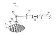
レーザスクライブ工程に用いられるレーザ加工機の一例を図3に示す。図3は、レーザ加工機の構成を模式的に示す斜視図である。
レーザ加工機300は、レーザ発振器301、コリメータレンズ302、マスク303、ベンドミラー304および集光レンズ305を備える。レーザ発振器301から出力されたレーザ光Lは、コリメータレンズ302に入射する。コリメータレンズ302は、レーザ光Lのビーム径を、マスク303に対応した適正値に調整する。コリメータレンズ302から出射したレーザ光Lは、マスク303に入射する。マスク303は、レーザ光Lのビーム径を、基板10に設けられたストリートの幅に対応するように整形する。マスク303を出射したレーザ光Lは、ベンドミラー304で反射された後、集光レンズ305に入射し、その後、基板10に照射される。An example of the laser processing machine used for the laser scribing process is shown in FIG. FIG. 3 is a perspective view schematically showing the configuration of the laser processing machine.
The
レーザ発振器301としては、パルスレーザ光を発振するパルスレーザ発振器が好ましい。連続発振と比較して、基板10に与える熱影響が小さいためである。レーザ光Lをパルス波形で発振する機構は特に限定されず、ビーム出力をメカニカルシャッターでオン(ON)/オフ(OFF)する方式、レーザ光Lの励起源をパルス制御する方式、ビーム出力をスイッチングする方式等が挙げられる。レーザ発振器301のレーザ発振機構も特に限定されず、レーザ発振の媒体として半導体を用いる半導体レーザ、媒体として炭酸ガス(CO2)等の気体を用いる気体レーザ、YAG等を用いる固体レーザ、および、ファイバレーザ等が挙げられる。これらは単独で、あるいは、2以上を組み合わせて用いられる。As the
基板10に照射されるレーザ光Lのパルス幅は特に限定されないが、熱影響が小さくなる点で、500ナノ秒以下であることが好ましく、200ナノ秒以下であることがより好ましい。レーザ光Lの波長も特に限定されないが、基板10によるレーザ光Lの吸収が高くなる点で、紫外線域(波長200〜400nm)であることが好ましい。レーザ光Lの周波数も特に限定されないが、例えば、1〜200kHzであり、高周波になるほど高速加工が可能となる。 The pulse width of the laser beam L irradiated to the
図3では、第1の浅溝111aを形成した後、レーザ光L(第2の浅溝用レーザ光L20および第2の溝用レーザ光L21)を連続的に照射して、1段階で第2の溝121を形成する態様を示している。また、第1のストリート(第1の浅溝111a)と第2のストリート(第2の溝121)とは直交している。この場合、後のプラズマダイシング工程により、矩形の素子チップ30が得られる。 In FIG. 3, after the first
(3)プラズマダイシング工程
次に、形成された第1の溝111および第2の溝121をプラズマに晒すことにより、各溝における基板10の厚み方向の残部をエッチングして、基板10を、素子領域130を備える複数の素子チップ30に分割する。このとき、第2層102の最外に配置されている保護膜は、素子領域130のマスクとして機能する。(3) Plasma Dicing Step Next, the formed
プラズマダイシング工程は、ハンドリング性の観点から、図4に示すように、基板10を支持部材22で支持した状態で行われることが好ましい。このとき、基板10の第2主面10Yを、支持部材22に当接させる。支持部材22の材質は特に限定されない。なかでも、基板10が支持部材22で支持された状態でダイシングされることを考慮すると、得られる素子チップ30がピックアップし易い点で、支持部材22は、柔軟性のある樹脂フィルムであることが好ましい。このとき、ハンドリング性の観点から、支持部材22はフレーム21に固定される。以下、フレーム21と、フレーム21に固定された支持部材22とを併せて、搬送キャリア20と称する。図4は、搬送キャリア20と支持部材22に支持された基板10とを示す上面図(a)およびY−Y線での断面図(b)である。 The plasma dicing step is preferably performed in a state where the
上記樹脂フィルムの材質は特に限定されず、例えば、ポリエチレンおよびポリプロピレン等のポリオレフィン、ポリエチレンテレフタレート等のポリエステル等の熱可塑性樹脂が挙げられる。樹脂フィルムには、伸縮性を付加するためのゴム成分(例えば、エチレン−プロピレンゴム(EPM)、エチレン−プロピレン−ジエンゴム(EPDM)等)、可塑剤、軟化剤、酸化防止剤、導電性材料等の各種添加剤が配合されていてもよい。また、上記熱可塑性樹脂は、アクリル基等の光重合反応を示す官能基を有していてもよい。 The material of the resin film is not particularly limited, and examples thereof include polyolefins such as polyethylene and polypropylene, and thermoplastic resins such as polyester such as polyethylene terephthalate. For resin films, rubber components for adding elasticity (eg, ethylene-propylene rubber (EPM), ethylene-propylene-diene rubber (EPDM), etc.), plasticizers, softeners, antioxidants, conductive materials, etc. These various additives may be blended. Moreover, the said thermoplastic resin may have a functional group which shows photopolymerization reactions, such as an acryl group.
支持部材22は、例えば、粘着剤を有する面(粘着面22a)と粘着剤を有しない面(非粘着面22b)とを備えている。粘着面22aの外周縁は、フレーム21の一方の面に貼着しており、フレーム21の開口を覆っている。粘着面22aのフレーム21の開口から露出した部分に、基板10の第2主面10Yが貼着されて支持される。プラズマ処理の際、支持部材22は、プラズマ処理ステージ(以下、単にステージと称す)と非粘着面22bとが接するように、ステージに載置される。 The
粘着面22aは、紫外線(UV)の照射によって粘着力が減少する粘着成分からなることが好ましい。これにより、プラズマダイシング後に素子チップ30をピックアップする際、UV照射を行うことにより、素子チップ30が粘着面22aから容易に剥離されて、ピックアップし易くなる。例えば、支持部材22は、樹脂フィルムの片面にUV硬化型アクリル粘着剤を、5〜20μmの厚みに塗布することにより得られる。 The
フレーム21は、基板10の全体と同じかそれ以上の面積の開口を有した枠体であり、所定の幅および略一定の薄い厚みを有している。フレーム21は、支持部材22および基板10を保持した状態で搬送できる程度の剛性を有している。フレーム21の開口の形状は特に限定されないが、例えば、円形や、矩形、六角形など多角形であってもよい。フレーム21には、位置決めのためのノッチ21aやコーナーカット21bが設けられていてもよい。フレーム21の材質としては、例えば、アルミニウム、ステンレス鋼等の金属や、樹脂等が挙げられる。 The
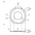
次に、図5を参照しながら、プラズマダイシング工程に使用されるプラズマ処理装置200を具体的に説明するが、プラズマ処理装置はこれに限定されるものではない。図5は、本実施形態に用いられるプラズマ処理装置200の構造の断面を概略的に示している。 Next, although the
プラズマ処理装置200は、ステージ211を備えている。搬送キャリア20は、支持部材22の基板10を保持している面(粘着面22a)が上方を向くように、ステージ211に搭載される。ステージ211の上方には、フレーム21および支持部材22の少なくとも一部を覆うとともに、基板10の少なくとも一部を露出させるための窓部224Wを有するカバー224が配置されている。 The
ステージ211およびカバー224は、反応室(真空チャンバ203)内に配置されている。真空チャンバ203は、上部が開口した概ね円筒状であり、上部開口は蓋体である誘電体部材208により閉鎖されている。真空チャンバ203を構成する材料としては、アルミニウム、ステンレス鋼(SUS)、表面をアルマイト加工したアルミニウム等が例示できる。誘電体部材208を構成する材料としては、酸化イットリウム(Y2O3)、窒化アルミニウム(AlN)、アルミナ(Al2O3)、石英(SiO2)等の誘電体材料が例示できる。誘電体部材208の上方には、上部電極としてのアンテナ209が配置されている。アンテナ209は、第1高周波電源210Aと電気的に接続されている。ステージ211は、真空チャンバ203内の底部側に配置される。The
真空チャンバ203には、ガス導入口203aが接続されている。ガス導入口203aには、原料ガスの供給原である原料ガス源(プロセスガス源212)およびアッシングガス源213が、それぞれ配管によって接続されている。また、真空チャンバ203には、排気口203bが設けられており、排気口203bには、真空チャンバ203内のガスを排気して減圧するための真空ポンプを含む減圧機構214が接続されている。 A
ステージ211は、それぞれ略円形の電極層215と、金属層216と、電極層215および金属層216を支持する基台217と、電極層215、金属層216および基台217を取り囲む外周部218とを備える。外周部218は導電性および耐エッチング性を有する金属により構成されており、電極層215、金属層216および基台217をプラズマから保護する。外周部218の上面には、円環状の外周リング229が配置されている。外周リング229は、外周部218の上面をプラズマから保護する役割をもつ。電極層215および外周リング229は、例えば、上記の誘電体材料により構成される。 The
電極層215の内部には、静電吸着機構を構成する電極部(以下、ESC電極219と称す。)と、第2高周波電源210Bに電気的に接続された高周波電極部220とが配置されている。ESC電極219には、直流電源226が電気的に接続されている。静電吸着機構は、ESC電極219および直流電源226により構成されている。 Inside the
金属層216は、例えば、表面にアルマイト被覆を形成したアルミニウム等により構成される。金属層216内には、冷媒流路227が形成されている。冷媒流路227は、ステージ211を冷却する。ステージ211が冷却されることにより、ステージ211に搭載された支持部材22が冷却されるとともに、ステージ211にその一部が接触しているカバー224も冷却される。これにより、基板10や支持部材22が、プラズマ処理中に加熱されることによって損傷されることが抑制される。冷媒流路227内の冷媒は、冷媒循環装置225により循環される。 The
ステージ211の外周付近には、ステージ211を貫通する複数の支持部222が配置されている。支持部222は、搬送キャリア20のフレーム21を支持する。支持部222は、昇降機構223Aにより昇降駆動される。搬送キャリア20が真空チャンバ203内に搬送されると、所定の位置まで上昇した支持部222に受け渡される。支持部222の上端面がステージ211と同じレベル以下にまで降下することにより、搬送キャリア20は、ステージ211の所定の位置に搭載される。 In the vicinity of the outer periphery of the
カバー224の端部には、複数の昇降ロッド221が連結しており、カバー224を昇降可能にしている。昇降ロッド221は、昇降機構223Bにより昇降駆動される。昇降機構223Bによるカバー224の昇降の動作は、昇降機構223Aとは独立して行うことができる。 At the end of the
制御装置228は、第1高周波電源210A、第2高周波電源210B、プロセスガス源212、アッシングガス源213、減圧機構214、冷媒循環装置225、昇降機構223A、昇降機構223Bおよび静電吸着機構を含むプラズマ処理装置200を構成する要素の動作を制御する。 The
プラズマは、基板10の残部(主に第1層101)がエッチングされる条件により発生させる。上記エッチング条件は、第1層101の材質に応じて適宜選択することができる。第1層101がSiの場合、各ストリート(溝)のエッチングには、いわゆるボッシュプロセスを用いることができる。ボッシュプロセスにおいては、堆積膜堆積ステップと、堆積膜エッチングステップと、Siエッチングステップとを順次繰り返すことにより、各溝を深さ方向に掘り進む。 The plasma is generated under the condition that the remainder of the substrate 10 (mainly the first layer 101) is etched. The etching conditions can be appropriately selected according to the material of the first layer 101. When the first layer 101 is Si, a so-called Bosch process can be used to etch each street (groove). In the Bosch process, each groove is dug in the depth direction by sequentially repeating the deposited film deposition step, the deposited film etching step, and the Si etching step.
堆積膜堆積ステップは、例えば、原料ガスとしてC4F8を150〜250sccmで供給しながら、真空チャンバ203内の圧力を15〜25Paに調整し、第1高周波電源210Aからアンテナ209への投入電力を1500〜2500Wとして、第2高周波電源210Bから高周波電極部220への投入電力を0Wとして、5〜15秒間、処理する条件で行われる。Deposition Film In the deposition step, for example, the pressure in the
堆積膜エッチングステップは、例えば、原料ガスとしてSF6を200〜400sccmで供給しながら、真空チャンバ203内の圧力を5〜15Paに調整し、第1高周波電源210Aからアンテナ209への投入電力を1500〜2500Wとして、第2高周波電源210Bから高周波電極部220への投入電力を100〜300Wとして、2〜10秒間、処理する条件で行われる。Deposited film etching step, for example, while supplying the SF6 as a source gas in 200~400Sccm, to adjust the pressure in the
Siエッチングステップは、例えば、原料ガスとしてSF6を200〜400sccmで供給しながら、真空チャンバ203内の圧力を5〜15Paに調整し、第1高周波電源210Aからアンテナ209への投入電力を1500〜2500Wとして、第2高周波電源210Bから高周波電極部220への投入電力を50〜200Wとして、10〜20秒間、処理する条件で行われる。In the Si etching step, for example, the pressure in the
上記のような条件で、堆積膜堆積ステップ、堆積膜エッチングステップ、および、Siエッチングステップを繰り返すことにより、各溝は、10μm/分の速度で深さ方向に垂直にエッチングされ得る。プラズマの発生においては、複数種類の原料ガスを併用してもよい。この場合、複数種類の原料ガスを時間差で真空チャンバ203内に導入してもよいし、複数種類の原料ガスを混合して、真空チャンバ203内に導入してもよい。 By repeating the deposition film deposition step, the deposition film etching step, and the Si etching step under the conditions as described above, each groove can be etched vertically in the depth direction at a rate of 10 μm / min. In the generation of plasma, plural kinds of source gases may be used in combination. In this case, a plurality of types of source gases may be introduced into the
このようにして、基板10は、支持部材22により支持された状態で、素子領域130を備える複数の素子チップ30に分割される。プラズマダイシング工程の終了後、支持部材22に支持された複数の素子チップ30は、ピックアップ工程に送られる。ピックアップ工程では、複数の素子チップ30は、それぞれ支持部材22から剥離されて、素子チップ30が得られる。 In this manner, the
プラズマダイシング工程の後、素子チップ30に残存する保護膜を、アッシングや洗浄により除去してもよい。このとき、レーザスクライブ工程において素子領域130上の保護膜に付着したデブリ140aは、保護膜とともに除去される。 After the plasma dicing process, the protective film remaining on the
本発明の素子チップの製造方法によれば、品質の高いプラズマダイシングが行われるため、種々の基板から素子チップを製造する方法として有用である。 According to the method of manufacturing an element chip of the present invention, high quality plasma dicing is performed, which is useful as a method of manufacturing an element chip from various substrates.
10:基板
10X:第1主面
10Y:第2主面
101:第1層
102:第2層
110:第1のストリート
111:第1の溝
111a:浅溝
120:第2のストリート
121:第2の溝
130:素子領域
140:不要物質
140a:デブリ
140b:盛り上がり
20:搬送キャリア
21:フレーム
21a:ノッチ
21b:コーナーカット
22:支持部材
22a:粘着面
22b:非粘着面
30:素子チップ
200:プラズマ処理装置
203:真空チャンバ
203a:ガス導入口
203b:排気口
208:誘電体部材
209:アンテナ
210A:第1高周波電源
210B:第2高周波電源
211:ステージ
212:プロセスガス源
213:アッシングガス源
214:減圧機構
215:電極層
216:金属層
217:基台
218:外周部
219:ESC電極
220:高周波電極部
221:昇降ロッド
222:支持部
223A、223B:昇降機構
224:カバー
224W:窓部
225:冷媒循環装置
226:直流電源
227:冷媒流路
228:制御装置
229:外周リング
300:レーザ加工機
301:レーザ発振器
302:コリメータレンズ
303:マスク
304:ベンドミラー
305:集光レンズ10:
Claims (5)
Translated fromJapanese前記複数のストリートに前記第1主面側からレーザ光を照射して、前記複数のストリートに対応する、前記基板の厚みよりも浅い複数の溝を形成するレーザスクライブ工程と、
前記レーザスクライブ工程の後、前記複数の溝をプラズマに晒すことにより、前記複数の溝における前記基板の厚み方向の残部をエッチングして、前記基板を、前記素子領域を備える複数の素子チップに分割するプラズマダイシング工程と、を備え、
前記複数のストリートが、第1のストリートと、前記第1のストリートと交差する第2のストリートと、を備え、
前記複数の溝が、前記第1のストリートに対応する第1の溝と、前記第2のストリートに対応する第2の溝と、を備え、
前記レーザスクライブ工程が、
前記第1のストリートに前記レーザ光をN1回(N1≧1)照射して、前記第1の溝よりも浅い第1の浅溝を形成する第1の浅溝形成工程と、
前記第1の浅溝形成工程の後、前記第2のストリートに前記レーザ光をM1回(M1≧1)照射して、前記第2の溝よりも浅い第2の浅溝を形成する第2の浅溝形成工程と、
前記第2の浅溝形成工程の後、前記第2の溝が形成されるまで、前記第2の浅溝にM2回(M2≧1)前記レーザ光を照射する第2の溝形成工程と、
前記第2の溝形成工程の後、前記第1の溝が形成されるまで、前記第1の浅溝にN2回(N2≧1)前記レーザ光を照射する第1の溝形成工程と、を備える、素子チップの製造方法。A first layer having a first main surface and a second main surface, a first layer being a semiconductor layer, and a second layer formed on the first main surface side of the first layer and having a protective film on the outermost side; Preparing a substrate comprising a plurality of element regions and a plurality of streets defining the element regions;
A laser scribing step of irradiating the plurality of streets with the laser light from the side of the first main surface to form a plurality of grooves corresponding to the plurality of streets and having a depth smaller than the thickness of the substrate;
After the laser scribing step, the plurality of grooves are exposed to plasma to etch the remaining portion of the plurality of grooves in the thickness direction of the substrate, thereby dividing the substrate into a plurality of element chips including the element region. And a plasma dicing process to
The plurality of streets comprises a first street and a second street intersecting the first street,
The plurality of grooves comprises a first groove corresponding to the first street and a second groove corresponding to the second street,
The laser scribing step is
A first shallow groove forming step of forming the first shallow groove shallower than the first groove by irradiating the first street with the laser light N1 times (N1 ≧ 1);
After the first shallow groove forming step, the second street is irradiated with the laser beam M1 times (M1 ≧ 1) to form a second shallow groove shallower than the second groove. Shallow groove formation process of
A second groove forming step of irradiating the second shallow groove M2 times (M2 ≧ 1) with the laser light until the second groove is formed after the second shallow groove forming step;
Afterpre-Symbol second groove forming step, a first groove forming step of irradiating the up first grooves are formed, N2 times the first shallow groove (N2 ≧ 1) the laser beam, A method of manufacturing an element chip, comprising:
前記M1と前記M2との和が2以上であり、前記第2の浅溝形成工程および前記第2の溝形成工程の前記第2のストリートへの前記レーザ光の照射が連続して行われる、請求項1〜4のいずれか一項に記載の素子チップの製造方法。The N1 is 2 or more, and the irradiation of the laser light to the first street in the first shallow groove forming step is continuously performed.
The sum of the M1 and the M2 is 2 or more, and the irradiation of the laser light to the second street in the second shallow groove forming step and the second groove forming step is performed continuously. The manufacturing method of the element chip as described in any one of Claims 1-4.
Priority Applications (2)
| Application Number | Priority Date | Filing Date | Title |
|---|---|---|---|
| JP2016243325AJP6524558B2 (en) | 2016-12-15 | 2016-12-15 | Method of manufacturing element chip |
| US15/811,733US10147646B2 (en) | 2016-12-15 | 2017-11-14 | Manufacturing process of element chip |
Applications Claiming Priority (1)
| Application Number | Priority Date | Filing Date | Title |
|---|---|---|---|
| JP2016243325AJP6524558B2 (en) | 2016-12-15 | 2016-12-15 | Method of manufacturing element chip |
Publications (2)
| Publication Number | Publication Date |
|---|---|
| JP2018098411A JP2018098411A (en) | 2018-06-21 |
| JP6524558B2true JP6524558B2 (en) | 2019-06-05 |
Family
ID=62561971
Family Applications (1)
| Application Number | Title | Priority Date | Filing Date |
|---|---|---|---|
| JP2016243325AActiveJP6524558B2 (en) | 2016-12-15 | 2016-12-15 | Method of manufacturing element chip |
Country Status (2)
| Country | Link |
|---|---|
| US (1) | US10147646B2 (en) |
| JP (1) | JP6524558B2 (en) |
Families Citing this family (5)
| Publication number | Priority date | Publication date | Assignee | Title |
|---|---|---|---|---|
| DE102017212858B4 (en)* | 2017-07-26 | 2024-08-29 | Disco Corporation | Method for processing a substrate |
| JP7005281B2 (en)* | 2017-10-31 | 2022-01-21 | 株式会社ディスコ | Processing method of work piece |
| CN109352184B (en)* | 2018-10-23 | 2021-02-09 | 深圳赛意法微电子有限公司 | Beam splitting laser cutting method for silicon-based wafer |
| US11784092B2 (en)* | 2020-02-27 | 2023-10-10 | Micron Technology, Inc. | Disposing protective cover film and underfill layer over singulated integrated circuit dice for protection during integrated circuit processing |
| US12230484B2 (en)* | 2021-10-13 | 2025-02-18 | Panasonic Intellectual Property Management Co., Ltd. | Plasma processing apparatus and plasma processing method |
Family Cites Families (10)
| Publication number | Priority date | Publication date | Assignee | Title |
|---|---|---|---|---|
| JP2005064231A (en) | 2003-08-12 | 2005-03-10 | Disco Abrasive Syst Ltd | How to divide a plate |
| JP4440036B2 (en)* | 2004-08-11 | 2010-03-24 | 株式会社ディスコ | Laser processing method |
| KR20120043933A (en)* | 2010-10-27 | 2012-05-07 | 삼성전자주식회사 | Method of fabricating a semiconductor device |
| KR20130081949A (en)* | 2012-01-10 | 2013-07-18 | 삼성전자주식회사 | Method for dicing wafer and method for manufacturing light emitting device chips using the same |
| US8652940B2 (en)* | 2012-04-10 | 2014-02-18 | Applied Materials, Inc. | Wafer dicing used hybrid multi-step laser scribing process with plasma etch |
| JP2015220240A (en)* | 2014-05-14 | 2015-12-07 | 株式会社ディスコ | Processing method for wafer |
| US10692765B2 (en)* | 2014-11-07 | 2020-06-23 | Applied Materials, Inc. | Transfer arm for film frame substrate handling during plasma singulation of wafers |
| JP6738591B2 (en)* | 2015-03-13 | 2020-08-12 | 古河電気工業株式会社 | Semiconductor wafer processing method, semiconductor chip, and surface protection tape |
| EP3376527A4 (en)* | 2015-11-09 | 2019-05-08 | Furukawa Electric Co., Ltd. | INTEGRATED MASK SURFACE PROTECTION FILM |
| WO2017082210A1 (en)* | 2015-11-09 | 2017-05-18 | 古河電気工業株式会社 | Method for manufacturing semiconductor chip, and mask-integrated surface protection tape used therein |
- 2016
- 2016-12-15JPJP2016243325Apatent/JP6524558B2/enactiveActive
- 2017
- 2017-11-14USUS15/811,733patent/US10147646B2/enactiveActive
Also Published As
| Publication number | Publication date |
|---|---|
| JP2018098411A (en) | 2018-06-21 |
| US10147646B2 (en) | 2018-12-04 |
| US20180174908A1 (en) | 2018-06-21 |
Similar Documents
| Publication | Publication Date | Title |
|---|---|---|
| JP7142236B2 (en) | Element chip manufacturing method | |
| JP6524558B2 (en) | Method of manufacturing element chip | |
| JP5023614B2 (en) | Semiconductor chip manufacturing method and semiconductor wafer processing method | |
| US10410924B2 (en) | Manufacturing process of element chip | |
| JP7357237B2 (en) | Manufacturing method of element chip | |
| CN107180789B (en) | Component chip and method for manufacturing the same | |
| JP2019114712A (en) | Method for manufacturing element chip | |
| JP7281709B2 (en) | Element chip manufacturing method | |
| CN107180787B (en) | Component chip and method for manufacturing the same | |
| US20220402072A1 (en) | Element chip manufacturing method and substrate processing method | |
| JP6519819B2 (en) | Method of manufacturing element chip | |
| US9941167B2 (en) | Method for manufacturing element chip | |
| JP6524535B2 (en) | Element chip and method of manufacturing the same | |
| JP7085342B2 (en) | Method of manufacturing element chips | |
| JP2018018980A (en) | Processing method for device wafer | |
| JP2006186263A (en) | Workpiece holding device | |
| US20220406660A1 (en) | Element chip manufacturing method and substrate processing method | |
| JP2020196023A (en) | Laser machining equipment, laser machining method, and device chip manufacturing method | |
| JP7149517B2 (en) | Element chip manufacturing method | |
| JP6775174B2 (en) | Method of manufacturing element chips | |
| JP2025008604A (en) | Manufacturing method of element chip | |
| JP2020194917A (en) | Method of manufacturing element chips | |
| JP2017163072A (en) | Device chip and method of manufacturing the same |
Legal Events
| Date | Code | Title | Description |
|---|---|---|---|
| A977 | Report on retrieval | Free format text:JAPANESE INTERMEDIATE CODE: A971007 Effective date:20181220 | |
| A131 | Notification of reasons for refusal | Free format text:JAPANESE INTERMEDIATE CODE: A131 Effective date:20190108 | |
| A521 | Request for written amendment filed | Free format text:JAPANESE INTERMEDIATE CODE: A523 Effective date:20190304 | |
| TRDD | Decision of grant or rejection written | ||
| A01 | Written decision to grant a patent or to grant a registration (utility model) | Free format text:JAPANESE INTERMEDIATE CODE: A01 Effective date:20190402 | |
| A61 | First payment of annual fees (during grant procedure) | Free format text:JAPANESE INTERMEDIATE CODE: A61 Effective date:20190418 | |
| R151 | Written notification of patent or utility model registration | Ref document number:6524558 Country of ref document:JP Free format text:JAPANESE INTERMEDIATE CODE: R151 |