JP6520880B2 - Electronic parts - Google Patents
Electronic partsDownload PDFInfo
- Publication number
- JP6520880B2 JP6520880B2JP2016187174AJP2016187174AJP6520880B2JP 6520880 B2JP6520880 B2JP 6520880B2JP 2016187174 AJP2016187174 AJP 2016187174AJP 2016187174 AJP2016187174 AJP 2016187174AJP 6520880 B2JP6520880 B2JP 6520880B2
- Authority
- JP
- Japan
- Prior art keywords
- coil
- nonmagnetic layer
- layer
- wiring
- nonmagnetic
- Prior art date
- Legal status (The legal status is an assumption and is not a legal conclusion. Google has not performed a legal analysis and makes no representation as to the accuracy of the status listed.)
- Active
Links
- 239000004020conductorSubstances0.000claimsdescription55
- 239000010410layerSubstances0.000description344
- 238000004519manufacturing processMethods0.000description9
- 239000011295pitchSubstances0.000description8
- 239000003990capacitorSubstances0.000description6
- 230000004907fluxEffects0.000description6
- 229910000859α-FeInorganic materials0.000description6
- 230000000694effectsEffects0.000description5
- 230000002093peripheral effectEffects0.000description4
- 229910017518Cu ZnInorganic materials0.000description3
- 229910017752Cu-ZnInorganic materials0.000description3
- 229910017943Cu—ZnInorganic materials0.000description3
- 238000010304firingMethods0.000description3
- 229910052802copperInorganic materials0.000description2
- TVZPLCNGKSPOJA-UHFFFAOYSA-Ncopper zincChemical compound[Cu].[Zn]TVZPLCNGKSPOJA-UHFFFAOYSA-N0.000description2
- 230000002500effect on skinEffects0.000description2
- 230000005012migrationEffects0.000description2
- 238000013508migrationMethods0.000description2
- 229910052709silverInorganic materials0.000description2
- XLYOFNOQVPJJNP-UHFFFAOYSA-NwaterSubstancesOXLYOFNOQVPJJNP-UHFFFAOYSA-N0.000description2
- HEZMWWAKWCSUCB-PHDIDXHHSA-N(3R,4R)-3,4-dihydroxycyclohexa-1,5-diene-1-carboxylic acidChemical compoundO[C@@H]1C=CC(C(O)=O)=C[C@H]1OHEZMWWAKWCSUCB-PHDIDXHHSA-N0.000description1
- 229910009369Zn MgInorganic materials0.000description1
- 229910007573Zn-MgInorganic materials0.000description1
- 238000003475laminationMethods0.000description1
- 239000000463materialSubstances0.000description1
- 239000002356single layerSubstances0.000description1
Images


Classifications
- H—ELECTRICITY
- H01—ELECTRIC ELEMENTS
- H01F—MAGNETS; INDUCTANCES; TRANSFORMERS; SELECTION OF MATERIALS FOR THEIR MAGNETIC PROPERTIES
- H01F27/00—Details of transformers or inductances, in general
- H01F27/006—Details of transformers or inductances, in general with special arrangement or spacing of turns of the winding(s), e.g. to produce desired self-resonance
- H—ELECTRICITY
- H01—ELECTRIC ELEMENTS
- H01F—MAGNETS; INDUCTANCES; TRANSFORMERS; SELECTION OF MATERIALS FOR THEIR MAGNETIC PROPERTIES
- H01F27/00—Details of transformers or inductances, in general
- H01F27/28—Coils; Windings; Conductive connections
- H01F27/2804—Printed windings
- H—ELECTRICITY
- H01—ELECTRIC ELEMENTS
- H01F—MAGNETS; INDUCTANCES; TRANSFORMERS; SELECTION OF MATERIALS FOR THEIR MAGNETIC PROPERTIES
- H01F1/00—Magnets or magnetic bodies characterised by the magnetic materials therefor; Selection of materials for their magnetic properties
- H01F1/0036—Magnets or magnetic bodies characterised by the magnetic materials therefor; Selection of materials for their magnetic properties showing low dimensional magnetism, i.e. spin rearrangements due to a restriction of dimensions, e.g. showing giant magnetoresistivity
- H01F1/0045—Zero dimensional, e.g. nanoparticles, soft nanoparticles for medical/biological use
- H01F1/0063—Zero dimensional, e.g. nanoparticles, soft nanoparticles for medical/biological use in a non-magnetic matrix, e.g. granular solids
- H—ELECTRICITY
- H01—ELECTRIC ELEMENTS
- H01F—MAGNETS; INDUCTANCES; TRANSFORMERS; SELECTION OF MATERIALS FOR THEIR MAGNETIC PROPERTIES
- H01F17/00—Fixed inductances of the signal type
- H01F17/0006—Printed inductances
- H01F17/0013—Printed inductances with stacked layers
- H—ELECTRICITY
- H01—ELECTRIC ELEMENTS
- H01F—MAGNETS; INDUCTANCES; TRANSFORMERS; SELECTION OF MATERIALS FOR THEIR MAGNETIC PROPERTIES
- H01F17/00—Fixed inductances of the signal type
- H01F17/04—Fixed inductances of the signal type with magnetic core
- H—ELECTRICITY
- H01—ELECTRIC ELEMENTS
- H01F—MAGNETS; INDUCTANCES; TRANSFORMERS; SELECTION OF MATERIALS FOR THEIR MAGNETIC PROPERTIES
- H01F27/00—Details of transformers or inductances, in general
- H01F27/28—Coils; Windings; Conductive connections
- H—ELECTRICITY
- H01—ELECTRIC ELEMENTS
- H01F—MAGNETS; INDUCTANCES; TRANSFORMERS; SELECTION OF MATERIALS FOR THEIR MAGNETIC PROPERTIES
- H01F27/00—Details of transformers or inductances, in general
- H01F27/28—Coils; Windings; Conductive connections
- H01F27/2847—Sheets; Strips
- H—ELECTRICITY
- H01—ELECTRIC ELEMENTS
- H01F—MAGNETS; INDUCTANCES; TRANSFORMERS; SELECTION OF MATERIALS FOR THEIR MAGNETIC PROPERTIES
- H01F27/00—Details of transformers or inductances, in general
- H01F27/28—Coils; Windings; Conductive connections
- H01F27/32—Insulating of coils, windings, or parts thereof
- H01F27/323—Insulation between winding turns, between winding layers
- H—ELECTRICITY
- H01—ELECTRIC ELEMENTS
- H01F—MAGNETS; INDUCTANCES; TRANSFORMERS; SELECTION OF MATERIALS FOR THEIR MAGNETIC PROPERTIES
- H01F41/00—Apparatus or processes specially adapted for manufacturing or assembling magnets, inductances or transformers; Apparatus or processes specially adapted for manufacturing materials characterised by their magnetic properties
- H01F41/02—Apparatus or processes specially adapted for manufacturing or assembling magnets, inductances or transformers; Apparatus or processes specially adapted for manufacturing materials characterised by their magnetic properties for manufacturing cores, coils, or magnets
- H01F41/04—Apparatus or processes specially adapted for manufacturing or assembling magnets, inductances or transformers; Apparatus or processes specially adapted for manufacturing materials characterised by their magnetic properties for manufacturing cores, coils, or magnets for manufacturing coils
- H01F41/041—Printed circuit coils
- H—ELECTRICITY
- H01—ELECTRIC ELEMENTS
- H01F—MAGNETS; INDUCTANCES; TRANSFORMERS; SELECTION OF MATERIALS FOR THEIR MAGNETIC PROPERTIES
- H01F17/00—Fixed inductances of the signal type
- H01F17/0006—Printed inductances
- H01F2017/0066—Printed inductances with a magnetic layer
- H—ELECTRICITY
- H01—ELECTRIC ELEMENTS
- H01F—MAGNETS; INDUCTANCES; TRANSFORMERS; SELECTION OF MATERIALS FOR THEIR MAGNETIC PROPERTIES
- H01F17/00—Fixed inductances of the signal type
- H01F17/0006—Printed inductances
- H01F2017/0073—Printed inductances with a special conductive pattern, e.g. flat spiral
- H—ELECTRICITY
- H01—ELECTRIC ELEMENTS
- H01F—MAGNETS; INDUCTANCES; TRANSFORMERS; SELECTION OF MATERIALS FOR THEIR MAGNETIC PROPERTIES
- H01F17/00—Fixed inductances of the signal type
- H01F17/0006—Printed inductances
- H01F2017/008—Electric or magnetic shielding of printed inductances
- H—ELECTRICITY
- H01—ELECTRIC ELEMENTS
- H01F—MAGNETS; INDUCTANCES; TRANSFORMERS; SELECTION OF MATERIALS FOR THEIR MAGNETIC PROPERTIES
- H01F27/00—Details of transformers or inductances, in general
- H01F27/28—Coils; Windings; Conductive connections
- H01F27/2804—Printed windings
- H01F2027/2809—Printed windings on stacked layers
Landscapes
- Engineering & Computer Science (AREA)
- Power Engineering (AREA)
- Microelectronics & Electronic Packaging (AREA)
- Chemical & Material Sciences (AREA)
- Health & Medical Sciences (AREA)
- Life Sciences & Earth Sciences (AREA)
- Manufacturing & Machinery (AREA)
- Biomedical Technology (AREA)
- General Health & Medical Sciences (AREA)
- Molecular Biology (AREA)
- Nanotechnology (AREA)
- Coils Or Transformers For Communication (AREA)
- Manufacturing Cores, Coils, And Magnets (AREA)
Description
Translated fromJapanese本発明は、電子部品に関する。 The present invention relates to an electronic component.
従来、電子部品としては、特開2006−318946号公報(特許文献1)に記載されたものがある。この電子部品は、磁性層および非磁性層を含む素体と、素体内に設けられ、螺旋状に巻き回されたコイルとを有する。コイルは、積層された複数層のコイル配線を含む。非磁性層は、積層方向に隣接するコイル配線間に位置する配線間部分と、コイルの径方向の外側に位置する径方向外側部分とを含む。 Conventionally, as an electronic component, there are some which were indicated in JP, 2006-318946, A (patent documents 1). This electronic component has an element including a magnetic layer and a nonmagnetic layer, and a coil provided in the element and wound in a spiral. The coil includes multiple layers of coil wiring stacked. The nonmagnetic layer includes an inter-wiring portion located between coil wires adjacent in the stacking direction, and a radially outer portion located radially outward of the coil.
ところで、前記従来の電子部品を製造して使用しようとすると、非磁性層の配線間部分および径方向外側部分にひびが発生するおそれがあることがわかった。このように、非磁性層の全体にひびが発生することで、素体の強度が不足する問題がある。 By the way, when it was going to manufacture and use the said conventional electronic component, it turned out that there exists a possibility that a crack may generate | occur | produce in the part between wiring of a nonmagnetic layer and a radial direction outer part. Thus, there is a problem that the strength of the element body is insufficient due to the generation of the crack in the entire nonmagnetic layer.
そこで、本発明の課題は、素体の強度不足を回避できる電子部品を提供することにある。 Then, the subject of this invention is providing the electronic component which can avoid the lack of strength of an element body.
前記課題を解決するため、本発明の電子部品は、
磁性層および非磁性層を含む素体と、
前記素体内に設けられ、螺旋状に巻き回されたコイルと
を備え、
前記コイルは、積層された複数層のコイル配線を含み、
前記非磁性層は、積層方向に隣接する少なくとも1組の前記コイル配線間に位置する配線間非磁性層と、前記コイルの径方向の外側または内側の少なくとも一方に位置する径方向非磁性層とを含み、
前記径方向非磁性層は、前記配線間非磁性層から離隔している。In order to solve the above-mentioned subject, electronic parts of the present invention,
An element including a magnetic layer and a nonmagnetic layer;
A helically wound coil provided in the body;
The coil includes multiple layers of coil wiring stacked,
The nonmagnetic layer is an interwiring nonmagnetic layer located between at least one set of coil wires adjacent in the stacking direction, and a radial nonmagnetic layer located at least one of the radially outer side and the inner side of the coil. Including
The radial nonmagnetic layer is separated from the interwiring nonmagnetic layer.
ここで、「径方向非磁性層は、配線間非磁性層から離隔している」とは、「全ての径方向非磁性層の何れも、全ての配線間非磁性層の何れにも接触していない」ことをいう。 Here, “the radial nonmagnetic layer is separated from the interwiring nonmagnetic layer” means “any one of all the radial nonmagnetic layers is in contact with any one of all the interwiring nonmagnetic layers. Not say that.
本発明の電子部品によれば、径方向非磁性層は、配線間非磁性層から離隔しているので、配線間非磁性層にひびが発生したとしても、配線間非磁性層のひびは径方向非磁性層に伝わらない。これにより、径方向非磁性層にひびが発生することを抑制し、素体の強度不足を回避できる。 According to the electronic component of the present invention, since the radial nonmagnetic layer is separated from the interwiring nonmagnetic layer, even if a crack occurs in the interwiring nonmagnetic layer, the crack in the interwiring nonmagnetic layer has a diameter It does not propagate to the direction nonmagnetic layer. As a result, the occurrence of cracks in the radial nonmagnetic layer can be suppressed, and insufficient strength of the element can be avoided.
また、電子部品の一実施形態では、前記コイル配線は、積層された複数層のコイル導体層から構成されている。 In one embodiment of the electronic component, the coil wiring is configured of a plurality of laminated coil conductor layers.
前記実施形態によれば、コイル配線は、積層された複数層のコイル導体層から構成されているので、コイル配線の抵抗を下げることができる。 According to the above-described embodiment, since the coil wiring is formed of the stacked plurality of coil conductor layers, the resistance of the coil wiring can be reduced.
また、電子部品の一実施形態では、
前記コイル配線は、積層された3層以上のコイル導体層から構成され、
前記径方向非磁性層は、前記3層以上のコイル導体層のうちの、積層方向の両側のコイル導体層の間に位置するコイル導体層と同一面上に配置されている。Also, in one embodiment of the electronic component:
The coil wiring is composed of three or more laminated coil conductor layers,
The radial nonmagnetic layer is disposed on the same plane as the coil conductor layer located between the coil conductor layers on both sides in the stacking direction among the three or more coil conductor layers.
前記実施形態によれば、径方向非磁性層は、積層方向の両側のコイル導体層の間に位置するコイル導体層と同一面上に配置されているので、径方向非磁性層を配線間非磁性層から一層離隔して配置することができる。 According to the embodiment, the radial nonmagnetic layer is disposed on the same plane as the coil conductor layer located between the coil conductor layers on both sides in the stacking direction. It can be disposed further apart from the magnetic layer.
また、電子部品の一実施形態では、前記コイル配線の厚さは、前記径方向非磁性層の厚さよりも厚い。 In one embodiment of the electronic component, the thickness of the coil wiring is thicker than the thickness of the radial nonmagnetic layer.
前記実施形態によれば、コイル配線の厚さは、径方向非磁性層の厚さよりも厚いので、径方向非磁性層を配線間非磁性層から一層離隔して配置することができる。 According to the embodiment, since the thickness of the coil wiring is larger than the thickness of the radial nonmagnetic layer, the radial nonmagnetic layer can be arranged further apart from the interwiring nonmagnetic layer.
また、電子部品の一実施形態では、前記径方向非磁性層は、前記コイル配線の厚さ方向の中央に位置する。 In one embodiment of the electronic component, the radial nonmagnetic layer is located at the center in the thickness direction of the coil wiring.
前記実施形態によれば、径方向非磁性層は、コイル配線の厚さ方向の中央に位置するので、径方向非磁性層を配線間非磁性層から一層離隔して配置することができる。 According to the embodiment, since the radial nonmagnetic layer is located at the center of the coil wiring in the thickness direction, the radial nonmagnetic layer can be arranged further apart from the interwiring nonmagnetic layer.
また、電子部品の一実施形態では、前記径方向非磁性層は、複数層からなる。 In one embodiment of the electronic component, the radial nonmagnetic layer is composed of a plurality of layers.
前記実施形態によれば、径方向非磁性層は、複数層からなるので、径方向非磁性層の厚みを厚くすることができ、直流重畳特性が向上する。 According to the embodiment, since the radial nonmagnetic layer is composed of a plurality of layers, the thickness of the radial nonmagnetic layer can be increased, and the DC bias characteristics are improved.
また、電子部品の一実施形態では、積層方向に隣り合う前記径方向非磁性層は、接触している。 In one embodiment of the electronic component, the radially nonmagnetic layers adjacent in the stacking direction are in contact with each other.
前記実施形態によれば、積層方向に隣り合う径方向非磁性層は、接触しているので、径方向非磁性層の厚みを厚くすることができ、直流重畳特性が向上する。 According to the embodiment, since the radial nonmagnetic layers adjacent in the stacking direction are in contact with each other, the thickness of the radial nonmagnetic layer can be increased, and the DC bias characteristics are improved.
また、電子部品の一実施形態では、前記配線間非磁性層は、複数層からなる。 In one embodiment of the electronic component, the inter-wiring nonmagnetic layer is composed of a plurality of layers.
前記実施形態によれば、配線間非磁性層は、複数層からなるので、配線間非磁性層にひびが入ってもショート不良の発生を防ぐことができる。 According to the embodiment, since the inter-wiring nonmagnetic layer is composed of a plurality of layers, the occurrence of a short failure can be prevented even if the inter-wiring nonmagnetic layer is cracked.
また、電子部品の一実施形態では、前記複数層の配線間非磁性層の側面は、凹凸を含み、該凹凸は、前記磁性層に入り込んでいる。 In one embodiment of the electronic component, the side surface of the plurality of inter-wiring nonmagnetic layers includes asperities, and the asperities intrude into the magnetic layer.
前記実施形態によれば、複数層の配線間非磁性層の側面の凹凸は、磁性層に入り込んでいるので、配線間非磁性層と磁性層の接触面積が増え、密着力が向上する。これにより、配線間非磁性層と磁性層の間でのはがれを抑制できる。 According to the embodiment, since the unevenness of the side surface of the plurality of inter-wiring nonmagnetic layers penetrates into the magnetic layer, the contact area between the inter-wiring nonmagnetic layer and the magnetic layer is increased, and the adhesion is improved. Thereby, peeling between the nonmagnetic layer between the interconnections and the magnetic layer can be suppressed.
また、電子部品の一実施形態では、前記配線間非磁性層の厚さは、前記径方向非磁性層の厚さよりも薄い。 In one embodiment of the electronic component, the thickness of the interwiring nonmagnetic layer is thinner than the thickness of the radial nonmagnetic layer.
前記実施形態によれば、配線間非磁性層の厚さは、径方向非磁性層の厚さよりも薄いので、コイル長が短くなり、交流損失を増加しつつ、直流重畳を向上できる。 According to the embodiment, since the thickness of the inter-wiring nonmagnetic layer is thinner than the thickness of the radial nonmagnetic layer, the coil length becomes short, and it is possible to improve the DC superposition while increasing the AC loss.
また、電子部品の一実施形態では、積層方向に隣接する全ての組の前記コイル配線間に、前記配線間非磁性層が配置されている。 In one embodiment of the electronic component, the inter-wiring nonmagnetic layer is disposed between the coil wires of all sets adjacent in the stacking direction.
前記実施形態によれば、積層方向に隣接する全ての組のコイル配線間に、配線間非磁性層が配置されているので、磁気飽和が一層発生しにくくなって、インダクタンス値を一層向上できる。 According to the embodiment, since the inter-wiring nonmagnetic layer is disposed between all pairs of coil wires adjacent in the stacking direction, magnetic saturation is further less likely to occur, and the inductance value can be further improved.
また、電子部品の一実施形態では、
前記コイル配線の側面は、凹凸を含み、該凹凸は、前記磁性層および前記径方向非磁性層の少なくとも一方に入り込んでいる。Also, in one embodiment of the electronic component:
The side surface of the coil wiring includes asperities, and the asperities enter at least one of the magnetic layer and the radial nonmagnetic layer.
前記実施形態によれば、コイル配線の側面の凹凸は、磁性層および径方向非磁性層の少なくとも一方に入り込んでいるので、コイル配線の表面積が大きくなり、表皮効果により高周波でのQ値を向上できる。 According to the embodiment, since the unevenness of the side surface of the coil wiring is in at least one of the magnetic layer and the radial nonmagnetic layer, the surface area of the coil wiring is increased, and the Q factor at high frequency is improved by the skin effect. it can.
本発明の電子部品によれば、径方向非磁性層は、配線間非磁性層から離隔しているので、径方向非磁性層にひびが発生することを抑制して、素体の強度不足を回避できる。 According to the electronic component of the present invention, since the radial nonmagnetic layer is separated from the inter-wiring nonmagnetic layer, generation of cracks in the radial nonmagnetic layer is suppressed, and the strength of the element is insufficient. It can be avoided.
上述したように、従来の電子部品では、非磁性層にひびが発生するおそれがあることがわかった。本願発明者は、この現象を鋭意検討したところ、以下の原因を見出した。
つまり、電子部品の製造において、磁性層、非磁性層およびコイル配線を積層してプレスする時に、コイル配線と非磁性層のヤング率の違いにより、非磁性層の配線間部分にひびが発生する。その後、焼成時に、配線間部分のひびが非磁性層の径方向外側部分に伝わり、この結果、径方向外側部分にもひびが発生する。このように、非磁性層の全体にひびが発生することで、素体の強度が不足することがわかった。
本発明は、本願発明者が独自に得た上記知見に基づいてなされたものである。As described above, it was found that in the conventional electronic component, the nonmagnetic layer may be cracked. The inventors of the present application have intensively studied this phenomenon and found the following causes.
That is, when the magnetic layer, the nonmagnetic layer, and the coil wiring are stacked and pressed in the manufacture of the electronic component, a crack is generated in the wiring portion of the nonmagnetic layer due to the difference in Young's modulus of the coil wiring and the nonmagnetic layer. . Thereafter, during firing, the cracks in the inter-wiring portion propagate to the radially outer portion of the nonmagnetic layer, and as a result, the cracks also occur in the radially outer portion. Thus, it was found that the strength of the element is insufficient due to the occurrence of the crack in the entire nonmagnetic layer.
The present invention has been made based on the above-described findings uniquely obtained by the inventor of the present invention.
以下、本発明を図示の実施の形態により詳細に説明する。 Hereinafter, the present invention will be described in detail by the illustrated embodiments.
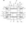
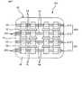
(第1実施形態)
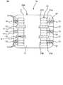
図1は、電子部品の第1実施形態を示す透視斜視図である。図2は、図1のX−X断面図である。図1と図2に示すように、電子部品1は、積層インダクタであり、素体10と、素体10の内部に設けられた螺旋状のコイル20と、素体10に設けられコイル20に電気的に接続された第1外部電極30および第2外部電極40とを有する。図1では、コイル20を実線で描いて示す。図2では、第1外部電極30および第2外部電極40を省略して描いている。First Embodiment
FIG. 1 is a transparent perspective view showing a first embodiment of the electronic component. FIG. 2 is a cross-sectional view taken along line X-X of FIG. As shown in FIGS. 1 and 2, the electronic component 1 is a laminated inductor, and the
電子部品1は、第1、第2外部電極30,40を介して、図示しない回路基板の配線に電気的に接続される。電子部品1は、例えば、ノイズ除去フィルタとして用いられ、パソコン、DVDプレーヤー、デジカメ、TV、携帯電話、カーエレクトロニクスなどの電子機器に用いられる。この他にもパワーインダクタとして用いられることもあり、この場合、例えば、各種電子機器に内蔵されるDCDCコンバータ部分に用いられる。 The electronic component 1 is electrically connected to the wiring of the circuit board (not shown) via the first and second
素体10は、略直方体状に形成されている。素体10は、第1端面と、第1端面に対向する第2端面と、第1端面と第2端面との間の4つの側面とを有する。 The
第1外部電極30および第2外部電極40は、例えば、AgまたはCuなどの導電性材料から構成される。第1外部電極30は、第1端面側に設けられ、第2外部電極40は、第2端面側に設けられている。 The first
コイル20は、例えば、AgまたはCuなどの導電性材料から構成される。コイル20の一端は、第1外部電極30に接続し、コイル20の他端は、第2外部電極40に接続している。コイル20の軸Aは、第1端面および第2端面に平行な方向に沿って配置される。これにより、第1、第2外部電極30,40は、コイル20の磁束の妨げとならない。 The
コイル20は、軸Aに沿って積層された複数のコイル配線21を含む。コイル配線21は、平面状に巻回されて形成される。積層方向に隣り合うコイル配線21は、積層方向に延在する接続配線を介して、接続される。このように、複数のコイル配線21は、互いに電気的に直列に接続されながら、螺旋を構成している。 The
素体10は、磁性層11および非磁性層12,13,14を含む。磁性層11および非磁性層12,13,14は、コイル20の軸Aに沿って積層される。磁性層11は、例えば、Ni−Cu−Zn系フェライト、Cu−Zn系フェライト又はNi−Cu−Zn−Mg系フェライト等のフェライトを用いて形成される。非磁性層12,13,14は、例えば、Cu−Zn系非磁性フェライト等の非磁性フェライトを用いて形成される。
非磁性層12,13,14は、積層方向に隣接する少なくとも1組のコイル配線21間に位置する配線間非磁性層12と、コイル20の径方向の外側または内側の少なくとも一方に位置する径方向非磁性層13,14とを含む。径方向非磁性層13,14は、配線間非磁性層12から離隔している。詳しく述べると、全ての径方向非磁性層13,14の何れも、全ての配線間非磁性層12の何れにも接触しない。 The
配線間非磁性層12は、単体のコイル配線21の周囲に発生する磁束(小ループの磁束)を遮断できる。したがって、小ループの磁束が、全てのコイル配線21によって発生し全てのコイル配線21の中心を通過する磁束(大ループの磁束)に重畳することを低減して、インダクタンスへの影響を低減できる。 The inter-wiring
径方向非磁性層13,14は、コイル20の径方向の外側に位置する径方向外側非磁性層13と、コイル20の径方向の内側に位置する径方向内側非磁性層14とから構成される。径方向非磁性層13,14は、磁気飽和の発生を低減して、直流重畳特性を向上できる。各コイル配線21の径方向に対向する径方向非磁性層(径方向外側非磁性層13および径方向内側非磁性層14のそれぞれ)は、1層からなる。各コイル配線21の径方向に対向する径方向外側非磁性層13および径方向内側非磁性層14は、同一面に配置される。 The radial
ここで、配線間非磁性層12および径方向非磁性層13,14は、コイル配線21の同一周回上に位置する非磁性層を含まない。具体的に述べると、図1に示すように、コイル配線21は、周方向において、一部に隙間を有し、この隙間に、非磁性層が設けられる場合がある。つまり、この非磁性層は、コイル配線21の延在方向(同一周回上)に位置する。この非磁性層は、配線間非磁性層12および径方向非磁性層13,14と異なる。したがって、この非磁性層が、配線間非磁性層12および径方向非磁性層13,14と接触しても、配線間非磁性層12と径方向非磁性層13,14は、接触しないで離隔している。 Here, the interwiring
前記電子部品1によれば、径方向非磁性層13,14は、配線間非磁性層12から離隔しているので、配線間非磁性層12にひびが発生したとしても、配線間非磁性層12のひびは径方向非磁性層13,14に伝わらない。これにより、径方向非磁性層13,14にひびが発生することを抑制し、素体10の強度不足を回避できる。 According to the electronic component 1, since the radial
具体的に述べると、電子部品1の製造において、磁性層11、非磁性層12,13,14およびコイル配線21を積層してプレスする時に、コイル配線21と非磁性層12,13,14のヤング率の違いにより、積層方向に隣り合うコイル配線21に挟まれた配線間非磁性層12にひびKが発生する場合がある。その後、焼成時において、径方向非磁性層13,14は、配線間非磁性層12と一体に連続しないため、配線間非磁性層12のひびKは、径方向非磁性層13,14に伝わらない。この結果、径方向非磁性層13,14にひびKが発生しない。 Specifically, in the manufacture of the electronic component 1, when the
特に、径方向外側非磁性層13にひびが入らないので、配線間非磁性層12のひびが、径方向外側非磁性層13を介して、素体10の外側につながらない。このため、水がひびを介して素体10内に進入することを阻止でき、コイル配線21のマイグレーションの発生を防止できる。これに対して、従来例(特開2006−318946号公報)では、非磁性層の径方向外側部分にもひびが発生するため、非磁性層の配線間部分のひびが、径方向外側部分のひびを経由して、素体10の外側につながる。この結果、水がひびを介して素体10内に進入して、コイル配線のマイグレーションが発生する。 In particular, since the crack in the radially outer
図2に示すように、コイル配線21は、積層された複数層のコイル導体層210から構成されている。コイル導体層210の断面形状は、略台形に形成されている。このように、コイル配線21は、複数層のコイル導体層210から構成されているので、コイル配線21の抵抗を下げることができる。 As shown in FIG. 2, the
具体的に述べると、コイル配線21は、積層された3層のコイル導体層210から構成され、径方向非磁性層13,14は、3層のコイル導体層210のうちの、積層方向の両側のコイル導体層210の間に位置する中央のコイル導体層210と同一面上に配置されている。これにより、径方向非磁性層13,14を配線間非磁性層12から一層離隔して配置することができる。 Specifically, the
なお、コイル配線を4層以上のコイル導体層から構成してもよく、径方向非磁性層を、3層以上のコイル導体層のうちの、積層方向の両側のコイル導体層の間に位置する何れかのコイル導体層と同一面上に配置すればよい。または、コイル配線を単層のコイル導体層から構成してもよく、この場合、径方向非磁性層をコイル導体層よりも薄く形成して、径方向非磁性層が配線間非磁性層から離隔するようにしてもよい。 The coil wiring may be composed of four or more coil conductor layers, and the radial nonmagnetic layer is located between the coil conductor layers on both sides in the lamination direction among the three or more coil conductor layers. It may be disposed on the same plane as any of the coil conductor layers. Alternatively, the coil wiring may be formed of a single layer coil conductor layer, in which case the radial nonmagnetic layer is thinner than the coil conductor layer, and the radial nonmagnetic layer is separated from the intermagnetic nonmagnetic layer. You may do it.
また、コイル配線21の積層方向の厚さは、径方向非磁性層13,14の積層方向の厚さよりも厚い。これによれば、径方向非磁性層13,14を配線間非磁性層12から一層離隔して配置することができる。 Further, the thickness in the stacking direction of the
また、径方向非磁性層13,14は、コイル配線21の厚さ方向の中央に位置する。具体的に述べると、径方向非磁性層13,14の厚さ方向の中心線とコイル配線21の厚さ方向の中心線とが一致している。これによれば、径方向非磁性層13,14を配線間非磁性層12から一層離隔して配置することができる。 The radial
また、配線間非磁性層12の厚さを、径方向非磁性層13,14の厚さよりも薄くしてもよく、これによれば、コイル長が短くなり、交流損失を増加しつつ、直流重畳を向上できる。 In addition, the thickness of the inter-wiring
また、積層方向に隣接する全ての組のコイル配線21間に、配線間非磁性層12が配置されている。これによれば、配線間非磁性層12により磁気飽和が発生しにくくなって、インダクタンス値を向上できる。 The inter-wiring
また、コイル配線21(3層のコイル導体層210)の側面は、径方向の外周側の外側面21aと、径方向の内周側の内側面21bとを含む。外側面21aおよび内側面21bは、それぞれ、凹部と凸部が積層方向に交互に並んで構成される凹凸を含む。コイル配線21の側面21a,21bの凹凸は、磁性層11および径方向非磁性層13,14に入り込んでいる。これによれば、コイル配線21の表面積が大きくなり、表皮効果により高周波でのQ値を向上できる。なお、コイル配線21の側面21a,21bの凹凸は、磁性層11および径方向非磁性層13,14の少なくとも一方に入り込んでいればよい。 Further, the side surface of the coil wiring 21 (the three layers of coil conductor layers 210) includes an
次に、前記電子部品1の製造方法について説明する。 Next, a method of manufacturing the electronic component 1 will be described.
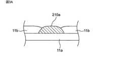
図3Aに示すように、第1磁性層11a上に、ペースト状の第1コイル導体層210aを塗布して乾燥する。そして、第1コイル導体層210aの両縁部を覆うと共に第1コイル導体層210aの両縁部以外の上面を露出させるように、第1磁性層11a上に、ペースト状の第2磁性層11bを塗布して乾燥する。 As shown in FIG. 3A, a paste-like first
その後、図3Bに示すように、第1コイル導体層210aの上面を覆うと共に第2磁性層11bの縁部を覆うように、第2コイル導体層210bを塗布して乾燥する。これにより、第2コイル導体層210bは、積層方向からみて、第1コイル導体層210aと重なる。 Thereafter, as shown in FIG. 3B, the second
そして、第2コイル導体層210bの径方向外側の縁部を覆うように、第1径方向外側非磁性層13aを塗布し、第2コイル導体層210bの径方向内側の縁部を覆うように、第1径方向内側非磁性層14aを塗布する。 Then, the first radially outer
その後、第2コイル導体層210bの上面を覆うと共に、第1径方向外側非磁性層13aの縁部および第1径方向内側非磁性層14aの縁部を覆うように、第3コイル導体層210cを塗布して乾燥する。これにより、第3コイル導体層210cは、積層方向からみて、第2コイル導体層210bと重なる。 Thereafter, the third
そして、第3コイル導体層210cの両縁部を覆うと共に第3コイル導体層210cの両縁部以外の上面を露出させるように、第1径方向外側非磁性層13aおよび第1径方向内側非磁性層14a上に、第3磁性層11cを塗布して乾燥する。 Then, the first radially outer
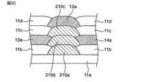
その後、図3Cに示すように、第3コイル導体層210cの上面を覆うと共に第3磁性層11cの縁部を覆うように、第1配線間非磁性層12aを塗布して乾燥する。これにより、第1配線間非磁性層12aは、積層方向からみて、第3コイル導体層210cと重なる。 Thereafter, as shown in FIG. 3C, the first inter-wiring
そして、第1配線間非磁性層12aの両縁部を覆うと共に第1配線間非磁性層12aの両縁部以外の上面を露出させるように、第3磁性層11c上に、第4磁性層11dを塗布して乾燥する。 Then, a fourth magnetic layer is formed on the third
その後、同様の工程を繰り返して、図3Dに示すように、第4コイル導体層210dおよび第5磁性層11eと、第5コイル導体層210e、第2径方向外側非磁性層13bおよび第2径方向内側非磁性層14bと、第6コイル導体層210fおよび第6磁性層11fとを、順に積層する。さらに、同様の工程を繰り返して、全ての層を積層してプレスし、その後焼成して、図2に示す電子部品1を製造する。 Thereafter, the same steps are repeated, and as shown in FIG. 3D, the fourth
(第2実施形態)
図4は、本発明の電子部品の第2実施形態を示す断面図である。第2実施形態は、第1実施形態とは、素体の構成が相違する。この相違する構成を以下に説明する。なお、第2実施形態において、第1実施形態と同一の符号は、第1実施形態と同じ構成であるため、その説明を省略する。Second Embodiment
FIG. 4 is a cross-sectional view showing a second embodiment of the electronic component of the present invention. The second embodiment is different from the first embodiment in the configuration of an element body. This different configuration is described below. In the second embodiment, the same reference numerals as those in the first embodiment denote the same components as those in the first embodiment, and thus the description thereof will be omitted.
図4に示すように、電子部品1Aの素体10Aの径方向非磁性層は、第1実施形態の径方向内側非磁性層14を含まず、径方向外側非磁性層13から構成される。第1実施形態と同様に、径方向外側非磁性層13は、配線間非磁性層12から離隔している。このように、径方向外側非磁性層13を設け、径方向内側非磁性層14を設けなくても、磁気飽和の抑制の効果を有し、直流重畳特性を向上できる。 As shown in FIG. 4, the radial nonmagnetic layer of the
(第3実施形態)
図5は、本発明の電子部品の第3実施形態を示す断面図である。第3実施形態は、第1実施形態とは、素体の構成が相違する。この相違する構成を以下に説明する。なお、第3実施形態において、第1実施形態と同一の符号は、第1実施形態と同じ構成であるため、その説明を省略する。Third Embodiment
FIG. 5 is a cross-sectional view showing a third embodiment of the electronic component of the present invention. The third embodiment is different from the first embodiment in the configuration of an element body. This different configuration is described below. In the third embodiment, the same reference numerals as those in the first embodiment have the same configurations as those in the first embodiment, and thus the description thereof will be omitted.
図5に示すように、電子部品1Bの素体10Bの径方向非磁性層は、第1実施形態の径方向外側非磁性層13を含まず、径方向内側非磁性層14から構成される。第1実施形態と同様に、径方向内側非磁性層14は、配線間非磁性層12から離隔している。このように、径方向内側非磁性層14を設け、径方向外側非磁性層13を設けなくても、磁気飽和の抑制の効果を有し、直流重畳特性を向上できる。 As shown in FIG. 5, the radial nonmagnetic layer of the
(第4実施形態)
図6は、本発明の電子部品の第4実施形態を示す断面図である。第4実施形態は、第1実施形態とは、素体およびコイル配線の構成が相違する。この相違する構成を以下に説明する。なお、第4実施形態において、第1実施形態と同一の符号は、第1実施形態と同じ構成であるため、その説明を省略する。Fourth Embodiment
FIG. 6 is a cross-sectional view showing a fourth embodiment of the electronic component of the present invention. The fourth embodiment is different from the first embodiment in the configuration of the element body and the coil wiring. This different configuration is described below. In the fourth embodiment, the same reference numerals as those in the first embodiment have the same configurations as those in the first embodiment, and thus the description thereof will be omitted.
図6に示すように、電子部品1Cのコイル20Cにおいて、コイル配線21Cは、4層のコイル導体層210から構成される。また、電子部品1Cの素体10Cにおいて、全てのコイル配線21Cのそれぞれの径方向に対向する径方向非磁性層13,14は、複数層からなる。具体的に述べると、各コイル配線21Cの径方向に対向する径方向外側非磁性層13および径方向内側非磁性層14のそれぞれは、2層からなる。2層の径方向外側非磁性層13は、積層方向に隣り合う。2層の径方向内側非磁性層14は、積層方向に隣り合う。 As shown in FIG. 6, in the coil 20C of the
最も下側のコイル配線21Cの径方向に対向する径方向非磁性層13,14において、積層方向に隣り合う2層の径方向外側非磁性層13は接触し、積層方向に隣り合う2層の径方向内側非磁性層14は接触している。 In the radially
中央のコイル配線21Cの径方向に対向する径方向非磁性層13,14において、積層方向に隣り合う2層の径方向外側非磁性層13は接触し、積層方向に隣り合う2層の径方向内側非磁性層14は接触している。 In radial direction
最も上側のコイル配線21Cの径方向に対向する径方向非磁性層13,14において、積層方向に隣り合う2層の径方向外側非磁性層13は、互いに離隔し、積層方向に隣り合う2層の径方向内側非磁性層14は、互いに離隔している。 In the radially
したがって、各コイル配線21Cの径方向に対向する径方向非磁性層13,14は、複数層からなるので、径方向非磁性層13,14の厚みを厚くすることができ、直流重畳特性が向上する。なお、少なくとも1つのコイル配線21Cの径方向に対向する径方向非磁性層が、複数層からなるようにしてもよい。 Therefore, since the radial
(第5実施形態)
図7は、本発明の電子部品の第5実施形態を示す断面図である。第5実施形態は、第1実施形態とは、素体の構成が相違する。この相違する構成を以下に説明する。なお、第5実施形態において、第1実施形態と同一の符号は、第1実施形態と同じ構成であるため、その説明を省略する。Fifth Embodiment
FIG. 7 is a cross-sectional view showing a fifth embodiment of the electronic component of the present invention. The fifth embodiment differs from the first embodiment in the configuration of the element body. This different configuration is described below. In the fifth embodiment, the same reference numerals as those in the first embodiment denote the same components as those in the first embodiment, and thus the description thereof will be omitted.
図7に示すように、電子部品1Dの素体10Dにおいて、全ての組のコイル配線21間のそれぞれに位置する配線間非磁性層12は、複数層からなる。具体的に述べると、各コイル配線21間の配線間非磁性層12は、2層からなる。したがって、1層の配線間非磁性層12にひびKが入っても、他の層の配線間非磁性層12によりショート不良の発生を防ぐことができる。なお、少なくとも1組のコイル配線間に位置する配線間非磁性層が、複数層からなるようにしてもよい。 As shown in FIG. 7, in the
また、複数層の配線間非磁性層12の側面は、径方向の外周側の外側面121と、径方向の内周側の内側面122とを含む。外側面121および内側面122は、それぞれ、凹部と凸部が積層方向に交互に並んで構成される凹凸を含む。複数層の配線間非磁性層12の側面121,122の凹凸は、磁性層11に入り込んでいる。したがって、配線間非磁性層12と磁性層11の接触面積が増え、密着力が向上する。これにより、配線間非磁性層12と磁性層11の間でのはがれを抑制できる。 Further, the side surfaces of the plurality of inter-wiring
(第6実施形態)
図8は、本発明の電子部品の第6実施形態を示す断面図である。第6実施形態は、第1実施形態とは、素体の構成が相違する。この相違する構成を以下に説明する。なお、第6実施形態において、第1実施形態と同一の符号は、第1実施形態と同じ構成であるため、その説明を省略する。Sixth Embodiment
FIG. 8 is a cross-sectional view showing a sixth embodiment of the electronic component of the present invention. The sixth embodiment is different from the first embodiment in the configuration of the element body. This different configuration is described below. In the sixth embodiment, the same reference numerals as those in the first embodiment have the same configurations as those in the first embodiment, and thus the description thereof will be omitted.
図8に示すように、電子部品1Eの素体10Eにおいて、配線間非磁性層12は、積層方向に隣接する全ての組(2組)のコイル配線21間でなく1組のコイル配線21間に設けられている。このように、配線間非磁性層12を、全ての組のコイル配線21間に設けないで、1組のコイル配線21間に設けても、磁気飽和の抑制の効果はあり、かつ、インダクタンス値を向上することができる。 As shown in FIG. 8, in the
(第7実施形態)
図9は、本発明の電子部品の第7実施形態を示す断面図である。第7実施形態は、第1実施形態とは、素体の構成が相違する。この相違する構成を以下に説明する。なお、第7実施形態において、第1実施形態と同一の符号は、第1実施形態と同じ構成であるため、その説明を省略する。Seventh Embodiment
FIG. 9 is a cross-sectional view showing a seventh embodiment of the electronic component of the present invention. The seventh embodiment is different from the first embodiment in the configuration of an element body. This different configuration is described below. In the seventh embodiment, the same reference numerals as those in the first embodiment have the same configurations as those in the first embodiment, and thus the description thereof will be omitted.
図9に示すように、電子部品1Fの素体10Fにおいて、一部の径方向非磁性層13,14は、コイル配線21に接触していない。具体的に述べると、積層方向中央のコイル配線21の径方向に対向する径方向非磁性層は、径方向内側非磁性層14からなり、径方向内側非磁性層14は、コイル配線21から離隔している。つまり、この径方向内側非磁性層14は、第1実施形態の径方向内側非磁性層と比べて、積層方向と直交する平面方向の大きさが小さくなっている。また、この径方向内側非磁性層14と同一面上に、径方向外側非磁性層13は設けられていない。 As shown in FIG. 9, in the
また、中央のコイル配線21と最も上側のコイル配線21の間の配線間非磁性層12に対向する径方向非磁性層は、径方向内側非磁性層14からなり、径方向内側非磁性層14は、当然に、配線間非磁性層12から離隔している。この径方向内側非磁性層14と同一面上に、径方向外側非磁性層13は設けられていない。 Further, the radial nonmagnetic layer facing the inter-wiring
また、最も下側のコイル配線21の径方向に対向する径方向非磁性層は、第1実施形態と同様に、径方向外側非磁性層13および径方向内側非磁性層14からなり、径方向外側非磁性層13および径方向内側非磁性層14は、コイル配線21に接触している。 Further, the radially nonmagnetic layer facing in the radial direction of the
このように、一部の径方向内側非磁性層14の平面方向の大きさが小さくなっていても、磁気飽和の抑制の効果を有し、直流重畳特性を向上できる。また、一部の径方向外側非磁性層13を省略しても、磁気飽和の抑制の効果を有し、直流重畳特性を向上できる。 As described above, even if the size in the plane direction of a part of the radially inner
(第8実施形態)
図10は、本発明の電子部品の第8実施形態を示す断面図である。第8実施形態は、第1実施形態とは、コンデンサを含む構成が相違する。この相違する構成を以下に説明する。なお、第8実施形態において、第1実施形態と同一の符号は、第1実施形態と同じ構成であるため、その説明を省略する。Eighth Embodiment
FIG. 10 is a cross-sectional view showing an eighth embodiment of the electronic component of the present invention. The eighth embodiment is different from the first embodiment in the configuration including a capacitor. This different configuration is described below. In the eighth embodiment, the same reference numerals as those in the first embodiment denote the same components as those in the first embodiment, and thus the description thereof will be omitted.
図10に示すように、電子部品1Gは、コイル20に加えて、コンデンサ5を含む。コンデンサ5は、積層方向に積層された第1電極層51、第2電極層52および第3電極層53を含む。第3電極層53は、第1電極層51と第2電極層52の間に離隔して配置される。 As shown in FIG. 10, the
第1電極層51は、コイル20の一端に電気的に接続され、第2電極層52は、コイル20の他端に電気的に接続され、第3電極層53は、グランドに接続される。これにより、第1電極層51と第3電極層53は、コイル20の一端に電気的に接続されたコンデンサとして機能し、第2電極層52と第3電極層53は、コイル20の他端に電気的に接続されたコンデンサとして機能して、電子部品1Gは、LCフィルタとして機能する。 The
したがって、電子部品1GをLCフィルタとしても、径方向非磁性層13,14は、配線間非磁性層12から離隔しているので、径方向非磁性層13,14にひびが発生することを抑制し、素体10の強度不足を回避できる。 Therefore, even when the
(第9実施形態)
図11は、本発明の電子部品の第9実施形態を示す断面図である。第9実施形態は、第1実施形態とは、コイルの数量が相違する。この相違する構成を以下に説明する。なお、第9実施形態において、第1実施形態と同一の符号は、第1実施形態と同じ構成であるため、その説明を省略する。The ninth embodiment
FIG. 11 is a cross-sectional view showing a ninth embodiment of the electronic component of the present invention. The ninth embodiment is different from the first embodiment in the number of coils. This different configuration is described below. In the ninth embodiment, the same reference numerals as those in the first embodiment have the same configurations as those in the first embodiment, and thus the description thereof will be omitted.
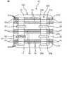
図11に示すように、電子部品1Hは、第1コイル201と第2コイル202とを有する。第1コイル201と第2コイル202は、同心状に配置され、磁気結合している。すなわち、電子部品1Hは、コモンモードチョークコイルとして機能する。 As shown in FIG. 11, the
第1コイル201は、第1コイル配線211と第2コイル配線212とを有する。第1コイル配線211と第2コイル配線212は、同心状に配置されている。第1コイル配線211と第2コイル配線212は、それぞれ、平面スパイラル状に形成されている。第1コイル配線211と第2コイル配線212は、図示しない接続導体を介して、直列に接続されている。第1コイル配線211と第2コイル配線212は、それぞれ、3層のコイル導体層210から構成されている。 The
第2コイル202は、第3コイル配線213と第4コイル配線214とを有する。第3コイル配線213と第4コイル配線214は、同心状に配置されている。第3コイル配線213と第4コイル配線214は、それぞれ、平面スパイラル状に形成されている。第3コイル配線213と第4コイル配線214は、図示しない接続導体を介して、直列に接続されている。第3コイル配線213と第4コイル配線214は、それぞれ、3層のコイル導体層210から構成されている。 The
第1実施形態と同様に、第1コイル配線211と第2コイル配線212の間、第2コイル配線212と第3コイル配線213の間、第3コイル配線213と第4コイル配線214の間のそれぞれに、配線間非磁性層12が設けられている。また、第1コイル201および第2コイル202のそれぞれの径方向内側に、径方向内側非磁性層14が設けられ、第1コイル201および第2コイル202のそれぞれの径方向外側に、径方向外側非磁性層13が設けられている。径方向内側非磁性層14および径方向外側非磁性層13は、配線間非磁性層12から離隔している。 As in the first embodiment, between the
さらに、第1コイル201および第2コイル202のそれぞれに、配線ピッチ非磁性層15が設けられている。具体的に述べると、第1コイル配線211の配線のピッチ間に、配線ピッチ非磁性層15が設けられている。配線ピッチ非磁性層15は、径方向非磁性層13,14と同じ材料から構成される。第2コイル配線212、第3コイル配線213および第4コイル配線214についても、同様である。配線ピッチ非磁性層15は、配線間非磁性層12から離隔している。 Furthermore, the wiring pitch
したがって、電子部品1Hをコモンモードチョークコイルとしても、径方向非磁性層13,14および配線ピッチ非磁性層15は、配線間非磁性層12から離隔しているので、径方向非磁性層13,14および配線ピッチ非磁性層15にひびが発生することを抑制し、素体10の強度不足を回避できる。 Therefore, even if the
なお、本発明は上述の実施形態に限定されず、本発明の要旨を逸脱しない範囲で設計変更可能である。例えば、第1から第9実施形態のそれぞれの特徴点を様々に組み合わせてもよい。 In addition, this invention is not limited to the above-mentioned embodiment, A design change is possible in the range which does not deviate from the summary of this invention. For example, the feature points of the first to ninth embodiments may be combined variously.
1,1A〜1H 電子部品
5 コンデンサ
10,10A〜10F 素体
11 磁性層
12 配線間非磁性層
121 外側面
122 内側面
13 径方向外側非磁性層
14 径方向内側非磁性層
15 配線ピッチ非磁性層
20,20C コイル
21,21C コイル配線
21a 外側面
21b 内側面
210 コイル導体層
30 第1外部電極
40 第2外部電極
201 第1コイル
202 第2コイル
211 第1コイル配線
212 第2コイル配線
213 第3コイル配線
214 第4コイル配線
A コイルの軸1, 1A to 1H
Claims (10)
Translated fromJapanese前記素体内に設けられ、螺旋状に巻き回されたコイルと
を備え、
前記コイルは、積層された複数層のコイル配線を含み、
前記非磁性層は、積層方向に隣接する少なくとも1組の前記コイル配線間に位置する配線間非磁性層と、前記コイルの径方向の外側または内側の少なくとも一方に位置する径方向非磁性層とを含み、
前記径方向非磁性層は、前記配線間非磁性層から離隔し、
前記コイル配線は、積層された3層以上のコイル導体層から構成され、
前記径方向非磁性層は、前記3層以上のコイル導体層のうちの、積層方向の両側のコイル導体層の間に位置するコイル導体層と同一面上に配置されている、電子部品。An element including a magnetic layer and a nonmagnetic layer;
A helically wound coil provided in the body;
The coil includes multiple layers of coil wiring stacked,
The nonmagnetic layer is an interwiring nonmagnetic layer located between at least one set of coil wires adjacent in the stacking direction, and a radial nonmagnetic layer located at least one of the radially outer side and the inner side of the coil. Including
The radial nonmagnetic layer is separated from the interwiring nonmagnetic layer,
The coil wiring is composed of three or more laminated coil conductor layers,
The electronic component,wherein the radial nonmagnetic layer is disposed on the same plane as the coil conductor layer located between the coil conductor layers on both sides of the three or more coil conductor layers in the stacking direction .
Priority Applications (4)
| Application Number | Priority Date | Filing Date | Title |
|---|---|---|---|
| JP2016187174AJP6520880B2 (en) | 2016-09-26 | 2016-09-26 | Electronic parts |
| US15/708,231US10586647B2 (en) | 2016-09-26 | 2017-09-19 | Electronic component |
| KR1020170121795AKR102044603B1 (en) | 2016-09-26 | 2017-09-21 | Electronic component |
| CN201710865620.5ACN107871585B (en) | 2016-09-26 | 2017-09-22 | Electronic component |
Applications Claiming Priority (1)
| Application Number | Priority Date | Filing Date | Title |
|---|---|---|---|
| JP2016187174AJP6520880B2 (en) | 2016-09-26 | 2016-09-26 | Electronic parts |
Publications (2)
| Publication Number | Publication Date |
|---|---|
| JP2018056192A JP2018056192A (en) | 2018-04-05 |
| JP6520880B2true JP6520880B2 (en) | 2019-05-29 |
Family
ID=61685672
Family Applications (1)
| Application Number | Title | Priority Date | Filing Date |
|---|---|---|---|
| JP2016187174AActiveJP6520880B2 (en) | 2016-09-26 | 2016-09-26 | Electronic parts |
Country Status (4)
| Country | Link |
|---|---|
| US (1) | US10586647B2 (en) |
| JP (1) | JP6520880B2 (en) |
| KR (1) | KR102044603B1 (en) |
| CN (1) | CN107871585B (en) |
Families Citing this family (5)
| Publication number | Priority date | Publication date | Assignee | Title |
|---|---|---|---|---|
| JP6787016B2 (en)* | 2016-10-05 | 2020-11-18 | Tdk株式会社 | Manufacturing method of laminated coil parts |
| JP7272790B2 (en)* | 2018-12-28 | 2023-05-12 | 太陽誘電株式会社 | Laminated coil parts |
| CN109524215A (en)* | 2018-12-29 | 2019-03-26 | 矽力杰半导体技术(杭州)有限公司 | Transformer and its manufacturing method is laminated |
| JP7529136B2 (en)* | 2021-02-26 | 2024-08-06 | 株式会社村田製作所 | Inductor Components |
| WO2025052755A1 (en)* | 2023-09-08 | 2025-03-13 | 株式会社村田製作所 | Multilayer inductor |
Family Cites Families (14)
| Publication number | Priority date | Publication date | Assignee | Title |
|---|---|---|---|---|
| JP4873522B2 (en) | 2005-05-10 | 2012-02-08 | Fdk株式会社 | Multilayer inductor |
| CN101390176B (en)* | 2006-01-31 | 2012-06-13 | 日立金属株式会社 | Laminated component and module using same |
| EP2040272A4 (en)* | 2006-07-05 | 2017-04-19 | Hitachi Metals, Ltd. | Laminated component |
| JP5339398B2 (en) | 2006-07-12 | 2013-11-13 | Fdk株式会社 | Multilayer inductor |
| JP4539630B2 (en)* | 2006-09-19 | 2010-09-08 | Tdk株式会社 | Multilayer inductor |
| WO2009087928A1 (en)* | 2008-01-08 | 2009-07-16 | Murata Manufacturing Co., Ltd. | Open magnetic circuit stacked coil component and process for producing the open magnetic circuit stacked coil component |
| JP5240221B2 (en)* | 2010-03-25 | 2013-07-17 | Tdk株式会社 | Multilayer inductor and method for manufacturing multilayer inductor |
| JP5621573B2 (en)* | 2010-12-15 | 2014-11-12 | 株式会社村田製作所 | Coil built-in board |
| JP2012160506A (en)* | 2011-01-31 | 2012-08-23 | Toko Inc | Laminated type inductor |
| KR101332100B1 (en)* | 2011-12-28 | 2013-11-21 | 삼성전기주식회사 | Stacked Inductors |
| JP6149386B2 (en)* | 2012-04-13 | 2017-06-21 | 株式会社村田製作所 | Multilayer electronic components |
| KR20130123632A (en) | 2012-05-03 | 2013-11-13 | 삼성전기주식회사 | Laminated inductor and manufacturing method thereof |
| JP2014187276A (en)* | 2013-03-25 | 2014-10-02 | Fdk Corp | Multilayer inductor |
| JP5999119B2 (en)* | 2014-02-10 | 2016-09-28 | 株式会社村田製作所 | Inductor |
- 2016
- 2016-09-26JPJP2016187174Apatent/JP6520880B2/enactiveActive
- 2017
- 2017-09-19USUS15/708,231patent/US10586647B2/enactiveActive
- 2017-09-21KRKR1020170121795Apatent/KR102044603B1/enactiveActive
- 2017-09-22CNCN201710865620.5Apatent/CN107871585B/enactiveActive
Also Published As
| Publication number | Publication date |
|---|---|
| KR102044603B1 (en) | 2019-11-13 |
| KR20180034255A (en) | 2018-04-04 |
| JP2018056192A (en) | 2018-04-05 |
| CN107871585A (en) | 2018-04-03 |
| CN107871585B (en) | 2020-04-10 |
| US20180090261A1 (en) | 2018-03-29 |
| US10586647B2 (en) | 2020-03-10 |
Similar Documents
| Publication | Publication Date | Title |
|---|---|---|
| JP6520880B2 (en) | Electronic parts | |
| KR102093558B1 (en) | Multilayer inductor manufacturing method and multilayer inductor | |
| JP6524980B2 (en) | Laminated coil component and method of manufacturing the same | |
| JP6760247B2 (en) | Coil parts | |
| JP2019047015A (en) | Coil parts | |
| JP6235099B2 (en) | Common mode filter and manufacturing method thereof | |
| JP2017183663A (en) | Coil component | |
| CN107112112B (en) | Coil component | |
| JP6630915B2 (en) | Multilayer coil parts | |
| US12119162B2 (en) | Coil component | |
| WO2012144103A1 (en) | Laminated inductor element and method for manufacturing same | |
| JP7463937B2 (en) | Inductor Components | |
| JP2013207149A (en) | Toroidal coil | |
| JP2018206950A (en) | Coil component | |
| JP2016018812A (en) | Multilayer coil parts | |
| JP2006339617A (en) | Electronic component | |
| JP4661746B2 (en) | Multilayer inductor and manufacturing method thereof | |
| JP2012182285A (en) | Coil component | |
| JP6720945B2 (en) | Coil parts | |
| JP2007317892A (en) | Multilayer inductor | |
| JP2012182286A (en) | Coil component | |
| JP7059520B2 (en) | Multilayer inductor components and their manufacturing methods | |
| JPH0529147A (en) | Laminated chip transformer | |
| JP2003217935A (en) | Layered inductor array | |
| JP2006086175A (en) | Multilayer common-mode choke coil array and its manufacturing method |
Legal Events
| Date | Code | Title | Description |
|---|---|---|---|
| A621 | Written request for application examination | Free format text:JAPANESE INTERMEDIATE CODE: A621 Effective date:20180413 | |
| A977 | Report on retrieval | Free format text:JAPANESE INTERMEDIATE CODE: A971007 Effective date:20190116 | |
| A131 | Notification of reasons for refusal | Free format text:JAPANESE INTERMEDIATE CODE: A131 Effective date:20190122 | |
| A521 | Written amendment | Free format text:JAPANESE INTERMEDIATE CODE: A523 Effective date:20190322 | |
| TRDD | Decision of grant or rejection written | ||
| A01 | Written decision to grant a patent or to grant a registration (utility model) | Free format text:JAPANESE INTERMEDIATE CODE: A01 Effective date:20190402 | |
| A61 | First payment of annual fees (during grant procedure) | Free format text:JAPANESE INTERMEDIATE CODE: A61 Effective date:20190415 | |
| R150 | Certificate of patent or registration of utility model | Ref document number:6520880 Country of ref document:JP Free format text:JAPANESE INTERMEDIATE CODE: R150 |