JP6507567B2 - Optical element and image display device - Google Patents
Optical element and image display deviceDownload PDFInfo
- Publication number
- JP6507567B2 JP6507567B2JP2014220037AJP2014220037AJP6507567B2JP 6507567 B2JP6507567 B2JP 6507567B2JP 2014220037 AJP2014220037 AJP 2014220037AJP 2014220037 AJP2014220037 AJP 2014220037AJP 6507567 B2JP6507567 B2JP 6507567B2
- Authority
- JP
- Japan
- Prior art keywords
- light
- optical element
- diffraction element
- image
- pupil
- Prior art date
- Legal status (The legal status is an assumption and is not a legal conclusion. Google has not performed a legal analysis and makes no representation as to the accuracy of the status listed.)
- Active
Links
- 230000003287optical effectEffects0.000titleclaimsdescription102
- 210000001747pupilAnatomy0.000claimsdescription47
- 210000001508eyeAnatomy0.000claimsdescription25
- 210000005252bulbus oculiAnatomy0.000claimsdescription6
- 239000000463materialSubstances0.000description28
- 238000004519manufacturing processMethods0.000description11
- 239000011347resinSubstances0.000description9
- 229920005989resinPolymers0.000description9
- PPBRXRYQALVLMV-UHFFFAOYSA-NStyreneChemical compoundC=CC1=CC=CC=C1PPBRXRYQALVLMV-UHFFFAOYSA-N0.000description6
- 239000000758substrateSubstances0.000description6
- 238000000034methodMethods0.000description5
- 230000002093peripheral effectEffects0.000description4
- 239000004925Acrylic resinSubstances0.000description3
- 229920000178Acrylic resinPolymers0.000description3
- 239000004743PolypropyleneSubstances0.000description3
- 230000006866deteriorationEffects0.000description3
- 238000005401electroluminescenceMethods0.000description3
- 239000011521glassSubstances0.000description3
- 239000004033plasticSubstances0.000description3
- 229920003023plasticPolymers0.000description3
- 229920003229poly(methyl methacrylate)Polymers0.000description3
- 229920005668polycarbonate resinPolymers0.000description3
- 239000004431polycarbonate resinSubstances0.000description3
- 239000004926polymethyl methacrylateSubstances0.000description3
- -1polypropylenePolymers0.000description3
- 229920001155polypropylenePolymers0.000description3
- 239000010453quartzSubstances0.000description3
- VYPSYNLAJGMNEJ-UHFFFAOYSA-Nsilicon dioxideInorganic materialsO=[Si]=OVYPSYNLAJGMNEJ-UHFFFAOYSA-N0.000description3
- 238000004088simulationMethods0.000description3
- 201000009310astigmatismDiseases0.000description2
- 230000005540biological transmissionEffects0.000description2
- 238000004364calculation methodMethods0.000description2
- 238000010586diagramMethods0.000description2
- 210000003128headAnatomy0.000description2
- 239000000853adhesiveSubstances0.000description1
- 230000001070adhesive effectEffects0.000description1
- 230000015572biosynthetic processEffects0.000description1
- 238000007796conventional methodMethods0.000description1
- 230000007423decreaseEffects0.000description1
- 238000011161developmentMethods0.000description1
- 230000018109developmental processEffects0.000description1
- 238000006073displacement reactionMethods0.000description1
- 238000010030laminatingMethods0.000description1
- 239000004973liquid crystal related substanceSubstances0.000description1
Images


Landscapes
- Diffracting Gratings Or Hologram Optical Elements (AREA)
- Holo Graphy (AREA)
Description
Translated fromJapanese本発明は、光学素子、画像表示装置および光学素子の製造方法に関するものである。 The present invention relates to an optical element, an image display device, and a method of manufacturing an optical element.
近年、光源装置から射出した画像光を観察者の眼に導いて、観察者に画像(虚像)を観察させる画像表示装置が商品化されている。例えば、画像表示装置の一種であるヘッドマウントディスプレイでは、小型化、広画角化、高効率化に関する開発が行われている。このようなヘッドマウントディスプレイにおいては、観察者の目に画像光を導くための構成として画像光を入射方向とは異なる方向に回折によって偏向する回折光学素子を用いている。例えば、下記特許文献1に示すヘッドマウントディスプレイでは、反射型の回折光学素子を用いることで小型化が図られている。 2. Description of the Related Art In recent years, an image display apparatus has been commercialized that guides image light emitted from a light source device to the eye of the observer and causes the observer to observe an image (virtual image). For example, in the case of a head mounted display, which is a type of image display device, developments have been made on downsizing, wide angle of view, and high efficiency. In such a head mounted display, a diffractive optical element that deflects the image light in a direction different from the incident direction is used as a configuration for guiding the image light to the eyes of the observer. For example, in the head mounted display shown in Patent Document 1 below, miniaturization is achieved by using a reflective diffractive optical element.
ところで、回折光学素子を用いた場合、画像光として利用される1次回折光以外に、回折されることなく回折光学素子を透過もしくは反射される0次光が存在する。0次光の割合は、回折光学素子の仕様、波長、入射角度等に依存するものの、回折光学素子へ入射した光のうち0次光を無くすことは非常に困難である。
上記従来技術においても、回折光学素子により0次回折光が生じ、特に透過した成分が観察者とは反対側へ出射することでヘッドマウントディスプレイの使用者以外の他人にも観察されてしまい、セキュリティー上問題となっていた。By the way, when a diffractive optical element is used, zero-order light which is transmitted or reflected by the diffractive optical element without being diffracted exists other than the first-order diffracted light used as image light. Although the ratio of zero-order light depends on the specifications of the diffractive optical element, the wavelength, the incident angle, etc., it is very difficult to eliminate the zero-order light in the light incident on the diffractive optical element.
Also in the above-mentioned prior art, the zero-order diffracted light is generated by the diffractive optical element, and in particular, the transmitted component is emitted to the side opposite to the observer and is observed also by other persons than the head mount display user. It was a problem.
本発明はこのような事情に鑑みてなされたものであって、画像光が0次光として外部に出射されることを抑制してセキュリティー性を向上させた光学素子、画像表示装置および光学素子の製造方法を提供することを目的とする。 The present invention has been made in view of such circumstances, and it is an optical element, an image display device, and an optical element in which security is improved by suppressing that image light is emitted to the outside as zero-order light. The purpose is to provide a manufacturing method.
本発明の第1態様に従えば、画像光の少なくとも一部を観察者の瞳に向けて偏向する光学素子であって、前記画像光が入射する第1反射型回折素子と、前記第1反射型回折素子の前記瞳とは反対側に積層される第2反射型回折素子と、を含む積層体からなる光学素子が提供される。 According to a first aspect of the present invention, there is provided an optical element for deflecting at least a part of image light toward the pupil of an observer, wherein the first reflection-type diffractive element on which the image light is incident; An optical element comprising a laminate including: a second reflective diffractive element stacked on the side opposite to the pupil of the diffractive diffractive element is provided.
第1反射型回折素子に画像光が入射すると、1次回折光および0次回折光が生成される。1次回折光は観察者の瞳に入射するが、0次回折光の一部は第1反射型回折素子を透過して瞳と異なる方向に進む。
これに対して第1態様に係る光学素子を採用すれば、第1反射型回折素子を透過した透過0次回折光を第2反射型回折素子により1次回折光として瞳に集光させることができる。よって、光学素子を透過して外部に射出されてしまう透過光(0次回折光)の強度を低減することができる。したがって、光学素子における瞳と反対側にいる別の観察者に画像光(透過0次回折光)を視認させ難くするので、セキュリティー性を向上させることができる。When the image light is incident on the first reflective diffraction element, first-order diffracted light and zero-order diffracted light are generated. The first-order diffracted light enters the pupil of the observer, but a part of the zero-order diffracted light passes through the first reflective diffraction element and travels in a direction different from that of the pupil.
On the other hand, if the optical element according to the first aspect is employed, it is possible to condense the transmitted zeroth-order diffracted light transmitted through the first reflective diffraction element on the pupil as first-order diffracted light by the second reflective diffraction element. Therefore, the intensity of the transmitted light (0th-order diffracted light) transmitted through the optical element and emitted to the outside can be reduced. Therefore, it is difficult for another observer on the opposite side of the pupil of the optical element to visually recognize the image light (transmitted zeroth-order diffracted light), and security can be improved.
上記第1態様において、前記第1反射型回折素子および前記第2反射型回折素子は、互いの干渉縞の間隔が異なっている構成としてもよい。
この構成によれば、第2反射型回折素子で回折された後に第1反射型回折素子を透過した回折光を瞳に良好に集光させることができる。In the first aspect, the first reflective diffraction element and the second reflective diffraction element may be configured such that the distance between the interference fringes is different.
According to this configuration, the diffracted light that has been diffracted by the second reflective diffraction element and transmitted through the first reflective diffraction element can be well condensed on the pupil.
上記第1態様において、前記第2反射型回折素子は、前記第1反射型回折素子よりも前記干渉縞の間隔が狭い構成としてもよい。
この構成によれば、上述のように回折光を瞳に良好に集光させる構造を実現することができる。In the first aspect, the second reflective diffraction element may be configured such that the distance between the interference fringes is narrower than that of the first reflective diffraction element.
According to this configuration, it is possible to realize the structure for well condensing diffracted light on the pupil as described above.
上記第1態様において、前記第1反射型回折素子および前記第2反射型回折素子は、前記瞳の奥行方向の所定範囲に前記画像光を集光させるように偏向する素子であってもよい。
この構成によれば、画像光の集光位置にマージンを持たせることができるので、回折素子の製造が容易となる。In the first aspect, the first reflection-type diffraction element and the second reflection-type diffraction element may be elements that deflect the image light to condense in a predetermined range in the depth direction of the pupil.
According to this configuration, a margin can be given to the condensing position of the image light, so that the manufacture of the diffraction element becomes easy.
上記第1態様において、前記所定範囲は、前記瞳から眼球の回転中心までの距離に基づいて設定される構成としてもよい。
この構成によれば、画像光の集光位置のずれ量を瞳から眼球の回転中心までの距離に基づいて設定された許容範囲内に設定することができる。よって、眼球の回転により視界が切れる部分が発生するのを抑制することができ、良好な画像視認性を実現することができる。In the first aspect, the predetermined range may be set based on the distance from the pupil to the center of rotation of the eyeball.
According to this configuration, it is possible to set the amount of deviation of the condensing position of the image light within the allowable range set based on the distance from the pupil to the rotation center of the eyeball. Therefore, it is possible to suppress the occurrence of a part where the field of view is cut off by the rotation of the eyeball, and it is possible to realize good image visibility.
上記第1態様において、前記積層体は、湾曲形状を有する構成としてもよい。
この構成によれば、像面(画像光)の形状歪や非点収差を積層体の湾曲度合いにより補正することができる。In the first aspect, the laminate may have a curved shape.
According to this configuration, it is possible to correct shape distortion and astigmatism of the image plane (image light) by the degree of curvature of the laminate.
本発明の第2態様に従えば、光源からの光を走査して画像光を生成する画像光生成部と、上記第1態様の光学素子と、を備える画像表示装置が提供される。 According to a second aspect of the present invention, there is provided an image display device comprising an image light generation unit that scans light from a light source to generate image light, and the optical element of the first aspect.
第2態様に係る画像表示装置によれば、上記光学素子を備えるので、該画像表示装置自体も画像光を第三者に視認されるおそれが低いセキュリティー性に優れたものとなる。 According to the image display device of the second aspect, since the above-described optical element is provided, the image display device itself is excellent in security with a low possibility that the image light is viewed by a third party.
上記第2態様において、前記画像光生成部は、前記光学素子に向かう前記光源からの前記光の光路の途中に設けられた波長補償素子をさらに備え、前記波長補償素子は、前記光が入射する第3反射型回折素子と、前記第3反射型回折素子における前記光の入射面とは反対側に積層される第4反射型回折素子と、を含む構成としてもよい。
この構成によれば、光源からの光の波長が変動した際に生じる画像光の位置ずれを波長補償素子によって補償することができるので、観察者の瞳に良好に画像光を集光させることができる。
また、第3反射型回折素子および第4反射型回折素子により1次回折光が効率良く生成されるので、装置内において迷光となる0次回折光の強度が低下し、迷光による画像の劣化を抑制できる。In the second aspect, the image light generation unit further includes a wavelength compensation element provided on an optical path of the light from the light source toward the optical element, and the wavelength compensation element receives the light. It may be configured to include a third reflective diffraction element, and a fourth reflective diffraction element stacked on the side opposite to the light incident surface of the third reflective diffraction element.
According to this configuration, since the positional deviation of the image light generated when the wavelength of the light from the light source fluctuates can be compensated by the wavelength compensation element, the image light can be well condensed on the pupil of the observer. it can.
In addition, since the first-order diffracted light is efficiently generated by the third reflection-type diffraction element and the fourth reflection-type diffraction element, the intensity of zero-order diffracted light that becomes stray light in the device is reduced, and image deterioration due to stray light can be suppressed. .
本発明の第3態様に従えば、画像光を観察者の瞳に向けて偏向する光学素子の製造方法であって、前記画像光が入射する第1反射型回折素子を干渉露光により形成する第1工程と、第2反射型回折素子を干渉露光により形成する第2工程と、前記第1反射型回折素子の前記瞳とは反対側に前記第2反射型回折素子を貼り合せる第3工程と、を備え、前記第2工程においては、前記第2反射型回折素子の未露光材料に対して前記第1反射型回折素子の厚さだけ移動させた状態で前記干渉露光を行う光学素子の製造方法が提供される。 According to a third aspect of the present invention, there is provided a method of manufacturing an optical element for deflecting image light toward the pupil of an observer, wherein the first reflective diffraction element on which the image light is incident is formed by interference exposure. 1 step, a second step of forming a second reflective diffraction element by interference exposure, and a third step of bonding the second reflective diffraction element on the opposite side of the pupil of the first reflective diffraction element And, in the second step, manufacturing an optical element performing the interference exposure in a state of being moved by the thickness of the first reflective diffraction element with respect to the unexposed material of the second reflective diffraction element. A method is provided.
第3態様に係る光学素子の製造方法によれば、第1反射型回折素子の厚さを考慮して第2反射型回折素子を露光して形成するので、回折光を観察者の瞳に良好に集光可能な積層構造の光学素子を製造することができる。 According to the method of manufacturing an optical element in the third aspect, the second reflective diffraction element is formed by exposing the second reflective diffraction element in consideration of the thickness of the first reflective diffraction element, so that diffracted light is good for the observer's pupil. An optical element having a laminated structure that can collect light can be manufactured.
上記第3態様において、前記第2工程においては、前記第1反射型回折素子と同じ屈折率のダミー部材を用いて前記干渉露光を行う構成としてもよい。
この構成によれば、ダミー部材により第1反射型回折素子の屈折率を考慮して第2反射型回折素子を露光して形成するので、回折光を観察者の瞳に良好に精度良く集光させることができる光学素子を製造できる。In the third aspect, the interference exposure may be performed using a dummy member having the same refractive index as that of the first reflective diffraction element in the second step.
According to this configuration, the second reflection type diffraction element is formed by exposing the second reflection type diffraction element in consideration of the refractive index of the first reflection type diffraction element by the dummy member, so that the diffracted light is collected on the pupil of the observer with good accuracy. Can produce an optical element that can be
以下、本発明の実施の形態について、図面を参照して詳細に説明する。
なお、以下の説明で用いる図面は、特徴をわかりやすくするために、便宜上特徴となる部分を拡大して示している場合があり、各構成要素の寸法比率などが実際と同じであるとは限らない。Hereinafter, embodiments of the present invention will be described in detail with reference to the drawings.
In the drawings used in the following description, in order to make the features easy to understand, the features that are the features may be enlarged for the sake of convenience, and the dimensional ratio of each component may be limited to the same as the actual Absent.
(第1実施形態)
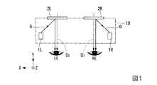
本実施形態に係る画像表示装置は、透過型のヘッドマウントディスプレイ(HMD:Head Mounted Display)である。図1は、本実施形態に係る透過型の表示装置としてのHMDを示す概略構成図である。First Embodiment
The image display apparatus according to the present embodiment is a transmissive head mounted display (HMD). FIG. 1 is a schematic configuration view showing an HMD as a transmission type display device according to the present embodiment.
以下、図面において必要に応じてXYZ座標系を用いて説明する。各図において、X方向とは透過型表示装置を装着する観察者の眼の配列方向、すなわち観察者の左右方向を規定し、Y方向とはX方向に直交し、観察者の前後方向を規定し、Z方向はXZ方向に直交する方向である鉛直方向を規定する。 The following description will be given using the XYZ coordinate system as needed in the drawings. In each figure, the X direction defines the arrangement direction of the eye of the observer wearing the transmissive display device, that is, the left and right direction of the observer, and the Y direction is orthogonal to the X direction and defines the anteroposterior direction of the observer The Z direction defines a vertical direction which is a direction orthogonal to the XZ direction.
本実施形態に係る表示装置10は、例えば、観察者の頭部に装着等によって画像を瞳に向けて表示可能なものである。表示装置10は、図1に示すように、使用者の左眼LEに重なる左眼用の光学素子2Lと、左眼用の画像光生成部1Lと、使用者の右眼REに重なる右眼用の光学素子2Rと、右眼用の画像光生成部1Rと、を備えている。 The
画像光生成部1Lは、画像光Gを光学素子2Lに向けて射出する。光学素子2Lは、透過した外光を観察者の左眼LEに入射させるとともに、画像光生成部1Lからの画像光Gを反射して観察者の左眼LEに集光する。 The
同様に、画像光生成部1Rは、画像光Gを光学素子2Rに向けて射出する。光学素子2Rは、透過した外光を観察者の右眼REに入射させるとともに、画像光生成部1Rからの画像光Gを反射して観察者の右眼REに集光する。 Similarly, the image
したがって、観察者は、光学素子2L及び光学素子2Rを介して観察される像と、画像光生成部1Lおよび画像光生成部1Rによる各表示画像と、を重畳した画像を知覚する。このように、観察者は、光学素子2L及び光学素子2Rを介して、表示装置10による表示画像と外界の画像(景色等)G1とを同時に見る(観察する)ことが可能であり、虚像を視認することができる。Therefore, the observer perceives an image in which the image observed through the
また、相互に視差が付与された立体視画像(左眼用画像および右眼用画像)を画像光生成部1Lおよび画像光生成部1Rに表示させることで、観察者に表示画像の立体感を知覚させることも可能である。 In addition, the stereoscopic image (the image for the left eye and the image for the right eye) to which parallax is given mutually is displayed on the image
画像光生成部1Rおよび画像光生成部1Lは、右眼用および左眼用の画像を生成する以外、同一の構造を有している。また、光学素子2R及び光学素子2Lも、右眼用および左眼用の画像を生成する以外、同一の構造を有している。
そのため、以下では画像光生成部1Rおよび光学素子2Rを例に挙げ、その構造について説明する。The
Therefore, in the following, the image
図2は画像光生成部1Rおよび光学素子2Rの周辺構成を示す概略図である。
図2に示すように、画像光生成部1Rは、光源11と、MEMSミラー12と、を含む。本実施形態において、光源11は青色、緑色、赤色のレーザー光を射出する複数のレーザー光源を含んでいる。MEMSミラー12は、レーザー光を反射することで光学素子2Rに入射させるマイクロミラーである。FIG. 2 is a schematic view showing the peripheral configuration of the image
As shown in FIG. 2, the image
画像光生成部1Rは、不図示の制御部からの画像信号に基づいて、MEMSミラー12により光源11から射出したレーザー光を走査して光学素子2Rに時間順次で入射させることで画像光Gを形成する。 The image
光学素子2Rは、入射する画像光Gを観察者の右眼REに入射させる。
光学素子2Rは、反射型回折素子が積層された構造を有する。本実施形態において、光学素子2Rは、反射型回折素子を2層積層した構造を有する。The
The
例えば、光学素子2Rは、図2に示すように、画像光Gが入射する光入射面側に配置された内面側回折素子(第1反射型回折素子)20と、該内面側回折素子20の光入射面20bと反対側の面20aに積層された外面側回折素子(第2反射型回折素子)30と、を備えている。
内面側回折素子20および外面側回折素子30は、反射型体積ホログラムにより構成され、画像光Gを観察者の右眼REの瞳に集光する。For example, as shown in FIG. 2, the
The inner surface
内面側回折素子20は、基材21と、回折部22と、を含む。
同様に、外面側回折素子30は、基材31と、回折部32と、を含む。
基材21および基材31は、プラスチック(例えば、PMMA、ポリカーボネ−ト樹脂、アクリル系樹脂、非晶性のポリプロピレン系樹脂、AS樹脂を含むスチレン系樹脂等)やガラス(例えば、石英やBK7等)から構成されている。The inner surface
Similarly, the outer surface side
The
回折部22および回折部32は、例えば、フォトポリマー材料から構成されており、内部から表面に亘って干渉縞がそれぞれ形成されている。この干渉縞は、後述のように球面波同士の干渉により形成される。 The
ここで、光学素子2R(内面側回折素子20および外面側回折素子30)の構造について説明する。 Here, the structure of the
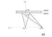
図3は、光学素子2Rのシミュレーションモデルを示した図である。
図3は、例えば、右眼REの位置に相当する集光点(0,0)からY軸方向に30mm離れた位置に内面側回折素子20(回折部22)、35mm離れた位置に外面側回折素子30(回折部32)が配置され、MEMSミラー12に相当する集光点が右眼REの集光点(0,0)の真下30mmにある場合の計算結果のグラフを示している。FIG. 3 is a diagram showing a simulation model of the
For example, FIG. 3 shows that the inner surface side diffraction element 20 (diffracting portion 22) is located 35 mm away from the focusing point (0, 0) corresponding to the position of the right eye RE in the Y axis direction, and the outer surface is located 35 mm away. The graph of a calculation result in case the diffraction element 30 (diffraction part 32) is arrange | positioned and the condensing point corresponded to the
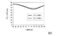
図4は、図3に基づいて求めた光学素子2Rの干渉縞の関係を示したシミュレーション結果を示すグラフである。図5は、図3に基づいて求めた光学素子2Rにおけるブラッグ角の関係を示したグラフである。なお、図4において、干渉縞間隔Aとは内面側回折素子20の回折部22の干渉縞間隔に対応し、干渉縞間隔Bとは外面側回折素子30の回折部32の干渉縞間隔に対応する。また、図5において、ブラッグ角Aとは回折部22のブラッグ角に対応し、ブラッグ角Bとは回折部32のブラッグ角に対応する。 FIG. 4 is a graph showing simulation results showing the relationship of interference fringes of the
図4に示されるように、体積ホログラム(回折部22および回折部32)のX座標が変化した場合、干渉縞の間隔が変化し、回折部22および回折部32の干渉縞の間隔の大小関係が逆転することがある。一般にHMDに使用されるX座標の範囲(約±10mm)に着目すれば、回折部32側の干渉縞の間隔の方が狭い。これは、同じX座標で回折部22および回折部32を比較した場合、図5に示されるように回折部32におけるブラッグ角の方が大きいことから導き出される。 As shown in FIG. 4, when the X coordinate of the volume hologram (the
ここで、干渉縞の間隔dは、ブラッグ条件d=λ/(sinθb×2)から導き出される。なお、λとは入射する光の波長であり、θbとはブラッグ角である。 Here, the spacing d of the interference fringes is derived from the Bragg condition d = λ / (sin θb × 2). Here, λ is the wavelength of incident light, and θb is the Bragg angle.
以上の計算結果に基づき、本実施形態では、内面側回折素子20および外面側回折素子30の同じX座標位置で回折部22および回折部32の干渉縞を比較した場合、内面側回折素子20の回折部22と外面側回折素子30の回折部32とは干渉縞の間隔を互いに異ならせている。具体的に、画像光に対して二層目に相当する回折部32について、回折部22よりも干渉縞の間隔を狭くしている。 Based on the above calculation results, in the present embodiment, when the interference fringes of the
以上のように、本実施形態の光学素子2Rは、上記内面側回折素子20および外面側回折素子30を積層した構造を有することで、画像光Gを回折させることで観察者の瞳に集光させることが可能である。 As described above, the
ところで、表示装置10が観察者に装着された状態では、観察者の瞳と光学素子2Rとの距離が一定となるが、観察者の瞳にピンポイントで画像光を集光させることは現実的に困難である。そこで、本実施形態の光学素子2Rは、瞳に対する画像光の集光位置に所定のマージンを有している。 By the way, in the state in which the
例えば、光学素子2Rは、瞳の奥行方向の所定範囲に画像光を集光させるように設計されている。すなわち、光学素子2Rは、画像光Gの焦点が瞳E1の奥行方向の所定範囲内に位置する。本実施形態では、図6に示すように、瞳の奥行方向における焦点の位置ずれ許容範囲Dとして、瞳位置に対して±12mmとした。 For example, the
この許容範囲Dの数値(±12mm)は、平均的な人の瞳から眼球回転中心までの距離に基づいて設定されるものである。この許容範囲を超えると、眼球の回転により視界が切れる部分が発生してしまい、画像の視認性が低下してしまうおそれがある。 The numerical value (± 12 mm) of the allowable range D is set based on the distance from the average human eye to the eyeball rotation center. If the allowable range is exceeded, a portion where the field of view is broken due to the rotation of the eye may occur, and the visibility of the image may be reduced.
本実施形態の光学素子2Rによれば、瞳の奥行方向の所定範囲(上記許容範囲D)内に画像光Gを集光させることができるので、眼球が回転した場合でも視界が切れてしまうことがなく、画像視認性に優れた表示装置10を提供することができる。 According to the
また、光学素子2Rの設計レベルとして、画像光Gを瞳にピンポイントで集光させるといった高いものが要求されないことから、ある程度の製造誤差が許容されるようになる。よって、光学素子2Rの製造が容易となり、結果的に低コスト化を図ることも可能である。 In addition, since a high level such as focusing the image light G on the pupil at a pinpoint is not required as a design level of the
続いて、光学素子2Rの製造方法について図面を参照にしながら説明する。
まず、内面側回折素子20を形成する。具体的に、基材21を用意し、基材21上に露光前のフォトポリマー材料(未露光材料)を塗布する。
そして、基材21上のフォトポリマー材料を干渉露光により露光して回折部22(干渉縞)を形成する(第1工程)。Subsequently, a method of manufacturing the
First, the
Then, the photopolymer material on the
このような干渉縞の形成方法は、従来の形成方法と同じとすればよい。図7は光学素子2Rの製造工程の要部として干渉縞の形成工程を示した図である。 The method of forming such interference fringes may be the same as that of the conventional method. FIG. 7 is a view showing a process of forming interference fringes as a main part of a process of manufacturing the
具体的には、例えば、図7(a)に示すように、フォトポリマー材料20Aに対し、一方の側の第1の所定の方向から物体光LBを照射するとともに、他方の側の第2の所定の方向から参照光LAを照射し、物体光LBと参照光LAとによって形成される干渉縞を、回折部22を構成するフォトポリマー材料20Aの内部に記録する。 Specifically, for example, as shown in FIG. 7A, the object light LB is irradiated to the
なお、第1の所定の方向、第2の所定の方向、物体光LB及び参照光LAの波長を適切に選択することで、回折部22における干渉縞のピッチを所望の値に設定することができる。 The pitch of the interference fringes in the
続いて、外面側回折素子30を形成する。具体的に、基材31を用意し、基材31上に露光前のフォトポリマー材料(未露光材料)を塗布する。
そして、基材31上のフォトポリマー材料を干渉露光により露光して回折部32(干渉縞)を形成する(第2工程)。Subsequently, the outer surface
Then, the photopolymer material on the
ところで、本実施形態の光学素子2Rは、内面側回折素子20および外面側回折素子30が積層されることで構成されている。ここで、外面側回折素子30で回折された光は、内面側回折素子20を透過する際に屈折した状態で観察者の瞳に射出される。そのため、外面側回折素子30に干渉縞を形成する際、内面側回折素子20の存在を考慮しないと、観察者の瞳位置からずれて、上述した許容範囲D外に画像光が集光してしまうおそれがある。 By the way, the
本実施形態では、上記課題を解決すべく、内面側回折素子20の厚み分だけ物体光LBから離す方向に移動した状態で回折部32を構成するフォトポリマー材料30Aを露光するようにしている。このように所定量だけ移動したフォトポリマー材料30Aに対し、一方の側の第1の所定の方向から物体光LBを照射するとともに、他方の側の第2の所定の方向から参照光LAを照射し、物体光LBと参照光LAとによって形成される干渉縞をフォトポリマー材料30Aの内部に記録することで回折部32を形成する。 In the present embodiment, in order to solve the above problem, the
なお、第1の所定の方向、第2の所定の方向、物体光LB及び参照光LAの波長を適切に選択することで、回折部32における干渉縞のピッチを上述のように回折部22における干渉縞のピッチよりも狭く形成することができる。 By appropriately selecting the first predetermined direction, the second predetermined direction, and the wavelengths of the object light LB and the reference light LA, the pitch of the interference fringes in the
最後に、内面側回折素子20および外面側回折素子30を不図示の接着剤により貼り合せて光学素子2Rの製造が完了する。 Finally, the inner surface
このような構成により光学素子2Rを製造すれば、内面側回折素子20の厚み分だけフォトポリマー材料30Aを移動した状態で露光するので、内面側回折素子20および外面側回折素子30が積層された状態で画像光を瞳に対して良好に集光させることができる。 If the
なお、内面側回折素子20の厚み分だけフォトポリマー材料30Aを移動した状態で露光する際、フォトポリマー材料30Aの前方(物体光LB側)に内面側回折素子20(基材21および回折部22)と同じ屈折率を有する光透過性部材(ダミー部材)90を配置するようにしてもよい。
このようにすれば、内面側回折素子20による屈折を考慮した状態で外面側回折素子30の回折部32の干渉縞が形成されるので、画像光を瞳に対してより高精度に集光させることができる。When the
In this way, the interference fringes of the
本実施形態の表示装置10では、図2に示したように、MEMSミラー12で走査されることで光学素子2Rに入射した画像光Gは、まず内面側回折素子20により1次回折光、0次回折光に分かれる。なお、さらに高次の回折光も生じる場合もあるが、これら高次の回折光は実用上問題とならないため、図示を省略している。 In the
0次回折光は、内面側回折素子20を透過する透過0次回折光L0と、該内面側回折素子20で反射される反射0次回折光(不図示)とを含む。The zeroth-order diffracted light includes transmitted zeroth-order diffracted light L0 transmitted through the inner surface
観察者の瞳には1次回折光のみが画像光Gとして入射する。一方、内面側回折素子20を透過する透過0次回折光L0は、画像情報を持ちながらも観察者の瞳とは反対方向へ進むため、迷光や観察者以外の他人に観察されてしまうおそれがある。Only first-order diffracted light is incident as image light G on the observer's pupil. On the other hand, transmission zero-order diffracted light L0 passing through the inner surface
これに対し、本実施形態の光学素子2Rでは、内面側回折素子20の光入射面と反対側に外面側回折素子30により内面側回折素子20で回折されずに透過した透過0次回折光L0の多くを回折して1次回折光L1として観察者の瞳に集光させることができる。その結果、光学素子2Rを透過して外部に射出されてしまう画像情報を持った光(透過0次回折光)の強度が低減するようになる。On the other hand, in the
したがって、本実施形態の表示装置10によれば、光学素子2Rにおける観察者の瞳と反対側にいる別の観察者に画像光(透過0次回折光)を視認させ難くすることができるので、セキュリティー性を備えた信頼性の高い画像表示を行うことができる。 Therefore, according to the
(第2実施形態)
続いて、本発明の第2実施形態について説明する。本実施形態と第1実施形態との違いは光学素子の構造であり、それ以外の構成は共通である。以下では、第1実施形態と共通の構成および部材については同じ符号を付し、その詳細な説明については省略する。Second Embodiment
Subsequently, a second embodiment of the present invention will be described. The difference between the present embodiment and the first embodiment is the structure of the optical element, and the other configuration is common. In the following, the same components and members as those of the first embodiment are denoted by the same reference numerals, and the detailed description thereof is omitted.
図8は本実施形態の光学素子の周辺構成を示す概略図である。
図8に示すように、本実施形態の光学素子40は、観察者の瞳側が凹んだ湾曲形状となっている。光学素子40は、上記実施形態と同様、画像光Gが入射する光入射面側に配置された内面側回折素子(第1反射型回折素子)120と、該内面側回折素子120の光入射面と反対側に積層された外面側回折素子(第2反射型回折素子)130と、を備えている。FIG. 8 is a schematic view showing the peripheral configuration of the optical element of the present embodiment.
As shown in FIG. 8, the
内面側回折素子120は、基材121と、回折部122と、を含む。
同様に、外面側回折素子130は、基材131と、回折部132と、を含む。
基材121および基材131は、プラスチック(例えば、PMMA、ポリカーボネ−ト樹脂、アクリル系樹脂、非晶性のポリプロピレン系樹脂、AS樹脂を含むスチレン系樹脂等)やガラス(例えば、石英やBK7等)から構成されている。
また、回折部122および回折部132は、例えば、フォトポリマー材料から構成されており、内部から表面に亘って干渉縞がそれぞれ形成されている。The inner surface
Similarly, the outer surface side
The
The
本実施形態の光学素子40によれば湾曲形状を呈しているため、像面(画像光G)の形状歪や非点収差を積層体の湾曲度合いにより補正することができる。よって、観察者は、歪みのない高品質な画像を視認することができる。 According to the
(第3実施形態)
続いて、本発明の第3実施形態について説明する。本実施形態と第1実施形態との違いは画像光生成部の構造であり、それ以外の構成は共通である。以下では、第1実施形態と共通の構成および部材については同じ符号を付し、その詳細な説明については省略する。Third Embodiment
Subsequently, a third embodiment of the present invention will be described. The difference between the present embodiment and the first embodiment is the structure of the image light generation unit, and the other configuration is common. In the following, the same components and members as those of the first embodiment are denoted by the same reference numerals, and the detailed description thereof is omitted.
図9は本実施形態の光学素子の周辺構成である画像光生成部を示す概略図である。
図9に示すように、本実施形態の画像光生成部50は、光源111と、MEMSミラー112と、波長補償素子113と、を含む。本実施形態において、光源111は青色、緑色、赤色のレーザー光を射出する複数のレーザー光源を含んでいる。MEMSミラー112は、レーザー光を反射することで光学素子2Rに入射させるマイクロミラーである。FIG. 9 is a schematic view showing an image light generation unit which is a peripheral configuration of the optical element of the present embodiment.
As shown in FIG. 9, the image
ところで、光源111を構成するレーザー光源は、例えば、変調する速度を速くする高速変調によって射出するレーザー光の波長が変化してしまうことがある。
光学素子2Rを構成する体積ホログラムは波長により回折角が異なるため、上述のようにレーザー光の波長が変化した場合に瞳に入射する画像光に位置ずれが生じ、画像が劣化する可能性がある。By the way, in the laser light source constituting the
Since the volume holograms constituting the
これに対し、本実施形態では、光源111の高速変調等による波長変化の影響を低減し投影画像の位置ずれ対策として波長補償素子113を用いている。波長補償素子113は、反射型回折光学素子を波長の変化した光に対して、波長の変化した光が光学素子2Rに入射する前に位置ずれを補償する方向に予め偏向させる素子として用いた。 On the other hand, in the present embodiment, the
波長補償素子113は、光学素子2Rと同様の構造を有している。例えば、波長補償素子113は、光源111からのレーザー光Lが入射する光入射面側に配置された内面側回折素子(第3反射型回折素子)60と、該内面側回折素子20の光入射面と反対側に積層された外面側回折素子(第4反射型回折素子)70と、を備えている。 The
内面側回折素子60は、基材61と、回折部62と、を含む。
同様に、外面側回折素子70は、基材71と、回折部72と、を含む。
基材61および基材71は、プラスチック(例えば、PMMA、ポリカーボネ−ト樹脂、アクリル系樹脂、非晶性のポリプロピレン系樹脂、AS樹脂を含むスチレン系樹脂等)やガラス(例えば、石英やBK7等)から構成されている。The inner surface
Similarly, the outer surface-
The base 61 and the base 71 may be made of plastic (for example, PMMA, polycarbonate resin, acrylic resin, amorphous polypropylene resin, styrene resin containing AS resin) or glass (for example, quartz or BK7 etc.) It consists of).
回折部62および回折部72は、例えば、フォトポリマー材料から構成されており、内部から表面に亘って干渉縞がそれぞれ形成されている。本実施形態において、回折部62および回折部72は、光学素子2R(回折部22および回折部32)と異なり、1次回折光を集光させる用途ではなく、略平行光入射および出射することができればよい。そのため、回折部62および回折部72はレンズ機能を有する必要が無く、入射位置によらず体積ホログラム全体で同じ干渉縞が記録されている。すなわち、回折部62および回折部72は、集光位置のずれの問題が生じないため、各々が同じ体積ホログラム(同じ干渉縞)となっている。 The diffractive portion 62 and the diffractive portion 72 are made of, for example, a photopolymer material, and interference fringes are formed from the inside to the surface, respectively. In the present embodiment, unlike the
このような構成に基づき、内面側回折素子60および外面側回折素子70は、光源111からのレーザー光Lを所定の回折角で回折してMEMSミラー112に入射させることが可能である。 Based on such a configuration, the inner surface
波長補償素子113に入射したレーザー光Lは、まず内面側回折素子60により1次回折光、0次回折光に分かれる。0次回折光のうち、内面側回折素子60を透過した光は、外面側回折素子70により回折されて1次回折光として射出される。 First, the laser beam L incident on the
本実施形態の波長補償素子113は、高速変調等に伴ってレーザー光Lの波長が変化して通常と異なる波長帯の成分(光学素子2Rにおいて所望の回折角が得られない成分)を含んだ場合でも、瞳に入射する画像光の位置ずれを抑制できる光としてMEMSミラー112に入射させることが可能である。 The
波長補償素子113は、画像光生成部50の光路の途中に設けられるため、1次回折光と同時に生じる0次光は表示装置10の光学系中で迷光となり画像劣化の原因となるおそれがある。波長補償素子113は、外面側回折素子70により内面側回折素子60で回折されずに透過した透過0次回折光の多くを回折して1次回折光としてMEMSミラー112に入射させることができる。その結果、装置内において迷光となる0次回折光の強度が低下し、迷光による画像の劣化を抑制できる。 Since the
以上、本発明の一実施形態について説明したが上記内容に限定されることはなく、発明の主旨を逸脱しない範囲において適宜変更可能である。 As mentioned above, although one Embodiment of this invention was described, it is not limited to the said content, It can change suitably in the range which does not deviate from the main point of invention.
上記実施形態では、内面側回折素子20および外面側回折素子30が、それぞれ基材21、31および回折部22、32を備える場合を例に挙げたが、本発明はこれに限定されない。例えば、内面側回折素子20および外面側回折素子30のいずれか一方が回折部のみから構成されていても良い。 In the said embodiment, although the case where the inner surface
例えば、外面側回折素子30が回折部32のみから構成されていても良い。この場合、回折部32として粘着性を有するフォトポリマー材料を用い、該フォトポリマー材料に干渉縞を形成した後に内面側回折素子20に貼付けることで光学素子2Rを形成すればよい。このようにすれば、基材31の数を減らすことにより、光学素子2Rの薄型化が可能となり、装置構成の小型化及び軽量化を図ることができる。 For example, the outer surface
また、上記実施形態では、画像光生成部1R、1Lとして、光源11からのレーザー光を水平走査及び垂直走査することで画像光Gを生成する構成を例に挙げたが、本発明はこれに限定されない。画像光生成部が、例えば、有機EL(Electro Luminescence)、無機EL、発光ダイオード(LED)といった発光素子から構成されていてもよい。あるいは、画像光生成部が、例えば、LED等の光源と液晶ライトバルブ或いはデジタルマイクロミラーデバイス(DMD)との組合せから構成されていても良い。 In the above embodiment, the image light G is generated by horizontally scanning and vertically scanning the laser light from the
G…画像光、E1…瞳、D…許容範囲、1R,1L…画像光生成部、2R,2L,40…光学素子、10…表示装置、11,111…光源、20,60…内面側回折素子(第1反射型回折素子)、20b…光入射面、20A,30A…フォトポリマー材料(未露光材料)、30,70,130…外面側回折素子(第2反射型回折素子)、90…光透過性部材(ダミー部材)、113…波長補償素子、120…内面側回折素子(第3反射型回折素子)、130…外面側回折素子(第4反射型回折素子)。 G: image light, E1: pupil, D: allowable range, 1R, 1L: image light generation unit, 2R, 2L, 40: optical element, 10: display device, 11, 111: light source, 20, 60: inside surface side diffraction Element (first reflection type diffraction element) 20b: Light incident surface 20A, 30A Photopolymer material (unexposed material) 30, 70, 130 Outer surface side diffraction element (second reflection type diffraction element) 90 Light transmitting member (dummy member) 113: wavelength compensation element 120: inner surface side diffraction element (third reflection type diffraction element) 130: outer surface side diffraction element (fourth reflection type diffraction element).
Claims (8)
Translated fromJapanese前記画像光が入射する第1反射型回折素子と、
前記第1反射型回折素子の前記瞳とは反対側に積層される第2反射型回折素子と、を含む積層体からなり、
第2反射型回折素子は、前記第1反射型回折素子を透過した透過0次回折光を回折し、1次回折光として前記瞳に向けて偏向するものであることを特徴とする光学素子。An optical element for deflecting at least a part of image light toward a pupil of an observer,
A first reflective diffraction element on which the image light is incident;
Ri Do a laminate and a second reflection type diffraction element to be laminated on the opposite side of the pupil of the first reflecting type diffractionelement,
An optical element characterized in thatthe second reflective diffraction element diffracts transmitted zero-order diffracted light transmitted through the first reflective diffraction element and deflects it as first-order diffracted light toward the pupil .
請求項1〜6のいずれか一項に記載の光学素子と、を備えることを特徴とする画像表示装置。An image light generator for scanning light from a light source to generate image light;
An image display apparatus comprising: the optical element according to any one of claims 1 to 6.
前記波長補償素子は、前記光が入射する第3反射型回折素子と、
前記第3反射型回折素子における前記光の入射面とは反対側に積層される第4反射型回折素子と、を含むことを特徴とする請求項7に記載の画像表示装置。The image light generation unit further includes a wavelength compensation element provided on an optical path of the light from the light source toward the optical element,
The wavelength compensation element is a third reflection type diffraction element on which the light is incident;
8. The image display apparatus according to claim 7, further comprising: a fourth reflection type diffraction element stacked on the side opposite to the light incident surface of the third reflection type diffraction element.
Priority Applications (1)
| Application Number | Priority Date | Filing Date | Title |
|---|---|---|---|
| JP2014220037AJP6507567B2 (en) | 2014-10-29 | 2014-10-29 | Optical element and image display device |
Applications Claiming Priority (1)
| Application Number | Priority Date | Filing Date | Title |
|---|---|---|---|
| JP2014220037AJP6507567B2 (en) | 2014-10-29 | 2014-10-29 | Optical element and image display device |
Publications (2)
| Publication Number | Publication Date |
|---|---|
| JP2016085428A JP2016085428A (en) | 2016-05-19 |
| JP6507567B2true JP6507567B2 (en) | 2019-05-08 |
Family
ID=55972601
Family Applications (1)
| Application Number | Title | Priority Date | Filing Date |
|---|---|---|---|
| JP2014220037AActiveJP6507567B2 (en) | 2014-10-29 | 2014-10-29 | Optical element and image display device |
Country Status (1)
| Country | Link |
|---|---|
| JP (1) | JP6507567B2 (en) |
Families Citing this family (7)
| Publication number | Priority date | Publication date | Assignee | Title |
|---|---|---|---|---|
| WO2018190007A1 (en) | 2017-04-13 | 2018-10-18 | ソニー株式会社 | Image display device |
| JP6958179B2 (en) | 2017-09-27 | 2021-11-02 | セイコーエプソン株式会社 | Display device |
| JP2019159203A (en)* | 2018-03-15 | 2019-09-19 | 株式会社リコー | Optical member, projection device, head-mounted display, head-up display, vehicle, spectrometer, and image forming apparatus |
| JP2020071429A (en) | 2018-11-01 | 2020-05-07 | セイコーエプソン株式会社 | Display device |
| KR102008776B1 (en)* | 2019-01-02 | 2019-08-08 | 김현석 | Optical functional pattern structure, apparatus for determining authenticity of an object and method of manufacturing same |
| KR102749298B1 (en)* | 2019-06-19 | 2025-01-10 | 송성의 | Barcode display apparatus having optical functional pattern structure and apparatus for determining authenticity of an object |
| JP2021086073A (en) | 2019-11-29 | 2021-06-03 | セイコーエプソン株式会社 | Image display device |
Family Cites Families (10)
| Publication number | Priority date | Publication date | Assignee | Title |
|---|---|---|---|---|
| JPS60254112A (en)* | 1984-05-31 | 1985-12-14 | Fujitsu Ltd | Light beam scanning device |
| JPH01147421A (en)* | 1987-12-03 | 1989-06-09 | Canon Inc | display system |
| JPH03188481A (en)* | 1989-12-18 | 1991-08-16 | Fujitsu Ltd | Multiple holograms and how to create them |
| JPH055804A (en)* | 1991-06-28 | 1993-01-14 | Fujitsu Ltd | Protective filter for laser |
| JPH08201718A (en)* | 1995-01-31 | 1996-08-09 | Nippondenso Co Ltd | Display device |
| JPH097212A (en)* | 1995-06-15 | 1997-01-10 | Asahi Glass Co Ltd | Optical head device |
| JP4089071B2 (en)* | 1999-03-10 | 2008-05-21 | ブラザー工業株式会社 | Head mounted camera |
| JP4518193B2 (en)* | 2008-06-10 | 2010-08-04 | ソニー株式会社 | Optical device and virtual image display device |
| KR20110050929A (en)* | 2009-11-09 | 2011-05-17 | 삼성전자주식회사 | Wearable Display |
| JP2013127489A (en)* | 2010-03-29 | 2013-06-27 | Panasonic Corp | See-through display |
- 2014
- 2014-10-29JPJP2014220037Apatent/JP6507567B2/enactiveActive
Also Published As
| Publication number | Publication date |
|---|---|
| JP2016085428A (en) | 2016-05-19 |
Similar Documents
| Publication | Publication Date | Title |
|---|---|---|
| JP6507567B2 (en) | Optical element and image display device | |
| JP6417589B2 (en) | OPTICAL ELEMENT, ELECTRO-OPTICAL DEVICE, WEARING TYPE DISPLAY DEVICE, AND OPTICAL ELEMENT MANUFACTURING METHOD | |
| CN105929535B (en) | Image display device | |
| EP2918402B1 (en) | Optical device, head mounted display, assembling method for the same, holographic diffraction grating, display device, and alignment device | |
| JP6287487B2 (en) | Optical device, image projection apparatus, and electronic apparatus | |
| JP5534009B2 (en) | Video display device, head-mounted display, and head-up display | |
| JP7371683B2 (en) | Image display device, image display method, and head mounted display | |
| JP6402991B2 (en) | Image display device | |
| JP6439453B2 (en) | Image display device and method of manufacturing image display device | |
| JP6477051B2 (en) | Image display device | |
| CN104423042A (en) | Optical device and image display device | |
| JP2017167181A (en) | Display device and light guide device | |
| JP2007279313A (en) | Method for manufacturing optical element, optical element, image display device and head mount display | |
| US12298506B2 (en) | Optical systems with low resolution peripheral displays | |
| JP2017173486A (en) | Optical element and display device | |
| KR20190099721A (en) | Holographic display apparatus providing expanded viewing window | |
| JP2021086073A (en) | Image display device | |
| JP2024531524A (en) | Optical system for directing display module light to a waveguide - Patents.com | |
| JP7293993B2 (en) | Display device | |
| CN112445114A (en) | Method for manufacturing optical element, and display device | |
| JP2016206495A (en) | Method for manufacturing diffractive optical element and image display device | |
| JP2010243786A (en) | Video display and head-mounted display | |
| US11906744B2 (en) | Display lens manufacturing apparatus and method, and head-mounted display device comprising display lens manufactured thereby | |
| US12379537B1 (en) | Optical systems with artifact blocking structures | |
| KR20140077378A (en) | Apparatus for head mounted display using holographic optical element lens |
Legal Events
| Date | Code | Title | Description |
|---|---|---|---|
| RD03 | Notification of appointment of power of attorney | Free format text:JAPANESE INTERMEDIATE CODE: A7423 Effective date:20160623 | |
| A621 | Written request for application examination | Free format text:JAPANESE INTERMEDIATE CODE: A621 Effective date:20171016 | |
| A977 | Report on retrieval | Free format text:JAPANESE INTERMEDIATE CODE: A971007 Effective date:20180717 | |
| A131 | Notification of reasons for refusal | Free format text:JAPANESE INTERMEDIATE CODE: A131 Effective date:20180807 | |
| RD05 | Notification of revocation of power of attorney | Free format text:JAPANESE INTERMEDIATE CODE: A7425 Effective date:20180919 | |
| RD02 | Notification of acceptance of power of attorney | Free format text:JAPANESE INTERMEDIATE CODE: A7422 Effective date:20180925 | |
| A521 | Written amendment | Free format text:JAPANESE INTERMEDIATE CODE: A523 Effective date:20180926 | |
| TRDD | Decision of grant or rejection written | ||
| A01 | Written decision to grant a patent or to grant a registration (utility model) | Free format text:JAPANESE INTERMEDIATE CODE: A01 Effective date:20190305 | |
| A61 | First payment of annual fees (during grant procedure) | Free format text:JAPANESE INTERMEDIATE CODE: A61 Effective date:20190318 | |
| R150 | Certificate of patent or registration of utility model | Ref document number:6507567 Country of ref document:JP Free format text:JAPANESE INTERMEDIATE CODE: R150 |