JP6501370B2 - Light emitting device - Google Patents
Light emitting deviceDownload PDFInfo
- Publication number
- JP6501370B2 JP6501370B2JP2017526636AJP2017526636AJP6501370B2JP 6501370 B2JP6501370 B2JP 6501370B2JP 2017526636 AJP2017526636 AJP 2017526636AJP 2017526636 AJP2017526636 AJP 2017526636AJP 6501370 B2JP6501370 B2JP 6501370B2
- Authority
- JP
- Japan
- Prior art keywords
- light
- emitting device
- exit surface
- light guide
- spectral distribution
- Prior art date
- Legal status (The legal status is an assumption and is not a legal conclusion. Google has not performed a legal analysis and makes no representation as to the accuracy of the status listed.)
- Active
Links
- 238000009826distributionMethods0.000claimsdescription63
- 230000003595spectral effectEffects0.000claimsdescription61
- 239000002223garnetSubstances0.000claimsdescription6
- 238000009795derivationMethods0.000claims1
- 239000000463materialSubstances0.000description45
- 230000003287optical effectEffects0.000description28
- OAICVXFJPJFONN-UHFFFAOYSA-NPhosphorusChemical compound[P]OAICVXFJPJFONN-UHFFFAOYSA-N0.000description22
- 239000000203mixtureSubstances0.000description21
- 239000000758substrateSubstances0.000description18
- 239000002096quantum dotSubstances0.000description10
- 238000004020luminiscence typeMethods0.000description9
- 238000006243chemical reactionMethods0.000description7
- 229910052684CeriumInorganic materials0.000description6
- 229910052771TerbiumInorganic materials0.000description6
- 239000011575calciumSubstances0.000description6
- 239000012530fluidSubstances0.000description6
- 239000011521glassSubstances0.000description6
- 230000008901benefitEffects0.000description5
- 230000017525heat dissipationEffects0.000description5
- 229910052727yttriumInorganic materials0.000description5
- RYGMFSIKBFXOCR-UHFFFAOYSA-NCopperChemical compound[Cu]RYGMFSIKBFXOCR-UHFFFAOYSA-N0.000description4
- 229910052693EuropiumInorganic materials0.000description4
- 229910052688GadoliniumInorganic materials0.000description4
- XEEYBQQBJWHFJM-UHFFFAOYSA-NIronChemical compound[Fe]XEEYBQQBJWHFJM-UHFFFAOYSA-N0.000description4
- 229910052779NeodymiumInorganic materials0.000description4
- 229910052777PraseodymiumInorganic materials0.000description4
- 229910052772SamariumInorganic materials0.000description4
- 229910052782aluminiumInorganic materials0.000description4
- 229910052791calciumInorganic materials0.000description4
- 229910052802copperInorganic materials0.000description4
- 239000010949copperSubstances0.000description4
- 229910052746lanthanumInorganic materials0.000description4
- 238000004064recyclingMethods0.000description4
- 229910010271silicon carbideInorganic materials0.000description4
- 229910052712strontiumInorganic materials0.000description4
- 229910052765LutetiumInorganic materials0.000description3
- XAGFODPZIPBFFR-UHFFFAOYSA-NaluminiumChemical compound[Al]XAGFODPZIPBFFR-UHFFFAOYSA-N0.000description3
- 229910052788bariumInorganic materials0.000description3
- 150000001875compoundsChemical class0.000description3
- 239000013078crystalSubstances0.000description3
- 230000000694effectsEffects0.000description3
- 238000002474experimental methodMethods0.000description3
- 239000007850fluorescent dyeSubstances0.000description3
- 229910052751metalInorganic materials0.000description3
- 239000002184metalSubstances0.000description3
- 239000007787solidSubstances0.000description3
- WUPHOULIZUERAE-UHFFFAOYSA-N3-(oxolan-2-yl)propanoic acidChemical compoundOC(=O)CCC1CCCO1WUPHOULIZUERAE-UHFFFAOYSA-N0.000description2
- OKTJSMMVPCPJKN-UHFFFAOYSA-NCarbonChemical compound[C]OKTJSMMVPCPJKN-UHFFFAOYSA-N0.000description2
- 229910052691ErbiumInorganic materials0.000description2
- 229910052775ThuliumInorganic materials0.000description2
- 229910052769YtterbiumInorganic materials0.000description2
- 239000005083Zinc sulfideSubstances0.000description2
- 230000002411adverseEffects0.000description2
- CSDREXVUYHZDNP-UHFFFAOYSA-NalumanylidynesiliconChemical compound[Al].[Si]CSDREXVUYHZDNP-UHFFFAOYSA-N0.000description2
- 239000006117anti-reflective coatingSubstances0.000description2
- 229910052980cadmium sulfideInorganic materials0.000description2
- 238000004364calculation methodMethods0.000description2
- 229910052799carbonInorganic materials0.000description2
- 239000011248coating agentSubstances0.000description2
- 238000000576coating methodMethods0.000description2
- 239000003086colorantSubstances0.000description2
- 238000004891communicationMethods0.000description2
- 238000013461designMethods0.000description2
- 238000005286illuminationMethods0.000description2
- 230000006872improvementEffects0.000description2
- 229910052742ironInorganic materials0.000description2
- 239000005355lead glassSubstances0.000description2
- 229910052744lithiumInorganic materials0.000description2
- 229910052749magnesiumInorganic materials0.000description2
- 229910052748manganeseInorganic materials0.000description2
- 229910052758niobiumInorganic materials0.000description2
- 229920000642polymerPolymers0.000description2
- 229910052700potassiumInorganic materials0.000description2
- 230000010076replicationEffects0.000description2
- 229910052701rubidiumInorganic materials0.000description2
- 229910052594sapphireInorganic materials0.000description2
- 239000010980sapphireSubstances0.000description2
- HBMJWWWQQXIZIP-UHFFFAOYSA-Nsilicon carbideChemical compound[Si+]#[C-]HBMJWWWQQXIZIP-UHFFFAOYSA-N0.000description2
- 229910052708sodiumInorganic materials0.000description2
- 229910052715tantalumInorganic materials0.000description2
- 229910052719titaniumInorganic materials0.000description2
- 229910052725zincInorganic materials0.000description2
- 239000011701zincSubstances0.000description2
- 229910052984zinc sulfideInorganic materials0.000description2
- 229910052726zirconiumInorganic materials0.000description2
- FRWYFWZENXDZMU-UHFFFAOYSA-N2-iodoquinolineChemical compoundC1=CC=CC2=NC(I)=CC=C21FRWYFWZENXDZMU-UHFFFAOYSA-N0.000description1
- 102100032047AlsinHuman genes0.000description1
- 101710187109AlsinProteins0.000description1
- 229910052582BNInorganic materials0.000description1
- PZNSFCLAULLKQX-UHFFFAOYSA-NBoron nitrideChemical compoundN#BPZNSFCLAULLKQX-UHFFFAOYSA-N0.000description1
- OYPRJOBELJOOCE-UHFFFAOYSA-NCalciumChemical compound[Ca]OYPRJOBELJOOCE-UHFFFAOYSA-N0.000description1
- GPXJNWSHGFTCBW-UHFFFAOYSA-NIndium phosphideChemical compound[In]#PGPXJNWSHGFTCBW-UHFFFAOYSA-N0.000description1
- 229910039444MoCInorganic materials0.000description1
- KWYUFKZDYYNOTN-UHFFFAOYSA-MPotassium hydroxideChemical compound[OH-].[K+]KWYUFKZDYYNOTN-UHFFFAOYSA-M0.000description1
- BQCADISMDOOEFD-UHFFFAOYSA-NSilverChemical compound[Ag]BQCADISMDOOEFD-UHFFFAOYSA-N0.000description1
- 229910001080W alloyInorganic materials0.000description1
- YNXRTZDUPOFFKZ-UHFFFAOYSA-N[In].[Ag]=SChemical compound[In].[Ag]=SYNXRTZDUPOFFKZ-UHFFFAOYSA-N0.000description1
- 238000010521absorption reactionMethods0.000description1
- 239000000853adhesiveSubstances0.000description1
- 230000001070adhesive effectEffects0.000description1
- XJBVBGUCNBMKIH-UHFFFAOYSA-Nalumane;rutheniumChemical compound[AlH3].[Ru]XJBVBGUCNBMKIH-UHFFFAOYSA-N0.000description1
- PNEYBMLMFCGWSK-UHFFFAOYSA-Naluminium oxideInorganic materials[O-2].[O-2].[O-2].[Al+3].[Al+3]PNEYBMLMFCGWSK-UHFFFAOYSA-N0.000description1
- JNDMLEXHDPKVFC-UHFFFAOYSA-Naluminum;oxygen(2-);yttrium(3+)Chemical compound[O-2].[O-2].[O-2].[Al+3].[Y+3]JNDMLEXHDPKVFC-UHFFFAOYSA-N0.000description1
- 238000004458analytical methodMethods0.000description1
- 229910052787antimonyInorganic materials0.000description1
- 230000009286beneficial effectEffects0.000description1
- LTPBRCUWZOMYOC-UHFFFAOYSA-Nberyllium oxideInorganic materialsO=[Be]LTPBRCUWZOMYOC-UHFFFAOYSA-N0.000description1
- 229910052793cadmiumInorganic materials0.000description1
- BDOSMKKIYDKNTQ-UHFFFAOYSA-Ncadmium atomChemical compound[Cd]BDOSMKKIYDKNTQ-UHFFFAOYSA-N0.000description1
- AQCDIIAORKRFCD-UHFFFAOYSA-Ncadmium selenideChemical compound[Cd]=[Se]AQCDIIAORKRFCD-UHFFFAOYSA-N0.000description1
- 229910010293ceramic materialInorganic materials0.000description1
- GWXLDORMOJMVQZ-UHFFFAOYSA-NceriumChemical compound[Ce]GWXLDORMOJMVQZ-UHFFFAOYSA-N0.000description1
- 230000008859changeEffects0.000description1
- 239000003795chemical substances by applicationSubstances0.000description1
- 239000012141concentrateSubstances0.000description1
- 238000001816coolingMethods0.000description1
- WUUZKBJEUBFVMV-UHFFFAOYSA-Ncopper molybdenumChemical compound[Cu].[Mo]WUUZKBJEUBFVMV-UHFFFAOYSA-N0.000description1
- SBYXRAKIOMOBFF-UHFFFAOYSA-Ncopper tungstenChemical compound[Cu].[W]SBYXRAKIOMOBFF-UHFFFAOYSA-N0.000description1
- PMHQVHHXPFUNSP-UHFFFAOYSA-Mcopper(1+);methylsulfanylmethane;bromideChemical compoundBr[Cu].CSCPMHQVHHXPFUNSP-UHFFFAOYSA-M0.000description1
- LCUOIYYHNRBAFS-UHFFFAOYSA-Ncopper;sulfanylideneindiumChemical compound[Cu].[In]=SLCUOIYYHNRBAFS-UHFFFAOYSA-N0.000description1
- 230000001419dependent effectEffects0.000description1
- 229910003460diamondInorganic materials0.000description1
- 239000010432diamondSubstances0.000description1
- 238000000609electron-beam lithographyMethods0.000description1
- 230000008030eliminationEffects0.000description1
- 238000003379elimination reactionMethods0.000description1
- 230000007613environmental effectEffects0.000description1
- 238000000605extractionMethods0.000description1
- 238000001914filtrationMethods0.000description1
- 230000004907fluxEffects0.000description1
- 229910052733galliumInorganic materials0.000description1
- PCHJSUWPFVWCPO-UHFFFAOYSA-NgoldChemical compound[Au]PCHJSUWPFVWCPO-UHFFFAOYSA-N0.000description1
- 229910052737goldInorganic materials0.000description1
- 239000010931goldSubstances0.000description1
- 229910002804graphiteInorganic materials0.000description1
- 239000010439graphiteSubstances0.000description1
- 229910052735hafniumInorganic materials0.000description1
- 238000010438heat treatmentMethods0.000description1
- 238000001093holographyMethods0.000description1
- 238000004519manufacturing processMethods0.000description1
- 238000000034methodMethods0.000description1
- 238000012986modificationMethods0.000description1
- 230000004048modificationEffects0.000description1
- 238000001127nanoimprint lithographyMethods0.000description1
- 230000004297night visionEffects0.000description1
- 125000002080perylenyl groupChemical groupC1(=CC=C2C=CC=C3C4=CC=CC5=CC=CC(C1=C23)=C45)*0.000description1
- 239000004038photonic crystalSubstances0.000description1
- 229940072033potashDrugs0.000description1
- 235000015320potassium carbonateNutrition0.000description1
- BWHMMNNQKKPAPP-UHFFFAOYSA-Lpotassium carbonateSubstances[K+].[K+].[O-]C([O-])=OBWHMMNNQKKPAPP-UHFFFAOYSA-L0.000description1
- 239000010453quartzSubstances0.000description1
- 238000010791quenchingMethods0.000description1
- 230000000171quenching effectEffects0.000description1
- 230000005855radiationEffects0.000description1
- 230000009467reductionEffects0.000description1
- 238000002310reflectometryMethods0.000description1
- 230000003362replicative effectEffects0.000description1
- 238000005488sandblastingMethods0.000description1
- 229920006395saturated elastomerPolymers0.000description1
- 239000004065semiconductorSubstances0.000description1
- 238000007493shaping processMethods0.000description1
- 229910052710siliconInorganic materials0.000description1
- 239000010703siliconSubstances0.000description1
- VYPSYNLAJGMNEJ-UHFFFAOYSA-Nsilicon dioxideInorganic materialsO=[Si]=OVYPSYNLAJGMNEJ-UHFFFAOYSA-N0.000description1
- 239000013464silicone adhesiveSubstances0.000description1
- 229910052709silverInorganic materials0.000description1
- 239000004332silverSubstances0.000description1
- 238000001228spectrumMethods0.000description1
- 238000006467substitution reactionMethods0.000description1
- 229910052718tinInorganic materials0.000description1
- 239000012780transparent materialSubstances0.000description1
- 238000011144upstream manufacturingMethods0.000description1
- 229910019901yttrium aluminum garnetInorganic materials0.000description1
- DRDVZXDWVBGGMH-UHFFFAOYSA-Nzinc;sulfideChemical compound[S-2].[Zn+2]DRDVZXDWVBGGMH-UHFFFAOYSA-N0.000description1
Images


Classifications
- G—PHYSICS
- G02—OPTICS
- G02B—OPTICAL ELEMENTS, SYSTEMS OR APPARATUS
- G02B6/00—Light guides; Structural details of arrangements comprising light guides and other optical elements, e.g. couplings
- G02B6/0001—Light guides; Structural details of arrangements comprising light guides and other optical elements, e.g. couplings specially adapted for lighting devices or systems
- G02B6/0003—Light guides; Structural details of arrangements comprising light guides and other optical elements, e.g. couplings specially adapted for lighting devices or systems the light guides being doped with fluorescent agents
- G—PHYSICS
- G02—OPTICS
- G02B—OPTICAL ELEMENTS, SYSTEMS OR APPARATUS
- G02B6/00—Light guides; Structural details of arrangements comprising light guides and other optical elements, e.g. couplings
- G02B6/0001—Light guides; Structural details of arrangements comprising light guides and other optical elements, e.g. couplings specially adapted for lighting devices or systems
- G02B6/0011—Light guides; Structural details of arrangements comprising light guides and other optical elements, e.g. couplings specially adapted for lighting devices or systems the light guides being planar or of plate-like form
- G02B6/0013—Means for improving the coupling-in of light from the light source into the light guide
- G02B6/0015—Means for improving the coupling-in of light from the light source into the light guide provided on the surface of the light guide or in the bulk of it
- G—PHYSICS
- G02—OPTICS
- G02B—OPTICAL ELEMENTS, SYSTEMS OR APPARATUS
- G02B6/00—Light guides; Structural details of arrangements comprising light guides and other optical elements, e.g. couplings
- G02B6/0001—Light guides; Structural details of arrangements comprising light guides and other optical elements, e.g. couplings specially adapted for lighting devices or systems
- G02B6/0011—Light guides; Structural details of arrangements comprising light guides and other optical elements, e.g. couplings specially adapted for lighting devices or systems the light guides being planar or of plate-like form
- G02B6/0013—Means for improving the coupling-in of light from the light source into the light guide
- G02B6/0023—Means for improving the coupling-in of light from the light source into the light guide provided by one optical element, or plurality thereof, placed between the light guide and the light source, or around the light source
- G—PHYSICS
- G02—OPTICS
- G02B—OPTICAL ELEMENTS, SYSTEMS OR APPARATUS
- G02B6/00—Light guides; Structural details of arrangements comprising light guides and other optical elements, e.g. couplings
- G02B6/0001—Light guides; Structural details of arrangements comprising light guides and other optical elements, e.g. couplings specially adapted for lighting devices or systems
- G02B6/0011—Light guides; Structural details of arrangements comprising light guides and other optical elements, e.g. couplings specially adapted for lighting devices or systems the light guides being planar or of plate-like form
- G02B6/0033—Means for improving the coupling-out of light from the light guide
- G02B6/005—Means for improving the coupling-out of light from the light guide provided by one optical element, or plurality thereof, placed on the light output side of the light guide
- G—PHYSICS
- G02—OPTICS
- G02B—OPTICAL ELEMENTS, SYSTEMS OR APPARATUS
- G02B6/00—Light guides; Structural details of arrangements comprising light guides and other optical elements, e.g. couplings
- G02B6/0001—Light guides; Structural details of arrangements comprising light guides and other optical elements, e.g. couplings specially adapted for lighting devices or systems
- G02B6/0011—Light guides; Structural details of arrangements comprising light guides and other optical elements, e.g. couplings specially adapted for lighting devices or systems the light guides being planar or of plate-like form
- G02B6/0066—Light guides; Structural details of arrangements comprising light guides and other optical elements, e.g. couplings specially adapted for lighting devices or systems the light guides being planar or of plate-like form characterised by the light source being coupled to the light guide
- G02B6/0068—Arrangements of plural sources, e.g. multi-colour light sources
- G—PHYSICS
- G02—OPTICS
- G02B—OPTICAL ELEMENTS, SYSTEMS OR APPARATUS
- G02B6/00—Light guides; Structural details of arrangements comprising light guides and other optical elements, e.g. couplings
- G02B6/0001—Light guides; Structural details of arrangements comprising light guides and other optical elements, e.g. couplings specially adapted for lighting devices or systems
- G02B6/0011—Light guides; Structural details of arrangements comprising light guides and other optical elements, e.g. couplings specially adapted for lighting devices or systems the light guides being planar or of plate-like form
- G02B6/0081—Mechanical or electrical aspects of the light guide and light source in the lighting device peculiar to the adaptation to planar light guides, e.g. concerning packaging
- G02B6/0085—Means for removing heat created by the light source from the package
Landscapes
- Physics & Mathematics (AREA)
- General Physics & Mathematics (AREA)
- Optics & Photonics (AREA)
- Planar Illumination Modules (AREA)
- Led Device Packages (AREA)
- Semiconductor Lasers (AREA)
- Light Guides In General And Applications Therefor (AREA)
- Optical Couplings Of Light Guides (AREA)
- Optical Filters (AREA)
- Non-Portable Lighting Devices Or Systems Thereof (AREA)
Description
Translated fromJapanese本発明は、動作時に第1のスペクトル分布を有する光を放射するように構成された光源と、第1のスペクトル分布を有する光を第2のスペクトル分布を有する光に変換するように構成された光ガイドとを備える発光デバイスに関する。 The present invention is configured to convert a light source having a first spectral distribution into a light having a second spectral distribution, and a light source configured to emit light having a first spectral distribution in operation. The invention relates to a light emitting device comprising a light guide.
高輝度光源、特に白色高輝度光源は、スポットライト、ヘッドランプ、舞台照明、及びデジタル光投影など様々な応用分野で関心が持たれている。このような用途では、短波長の光が透明度の高いルミネセンス材料中で長波長に変換される、いわゆるルミネセンス集光器を利用することができる。このような透明なルミネセンス材料をLEDで照明すると、ルミネセンス材料内で長い波長を生じる。ルミネセンス材料内を導波される変換光を表面から抽出すると、強度利得、換言すれば輝度の上昇が得られる。 High brightness light sources, in particular white high brightness light sources, are of interest in various applications such as spotlights, headlamps, stage lighting and digital light projection. In such applications, so-called luminescence collectors can be used, in which short wavelength light is converted to long wavelengths in highly transparent luminescent materials. Illumination of such transparent luminescent material with LEDs results in long wavelengths within the luminescent material. Extracting from the surface the converted light guided in the luminescent material provides an intensity gain, in other words an increase in brightness.
文献WO2012/056382号には、導波路とその導波路の表面に配置された2つの光源とを備える、このような目的のための照明デバイスが記載されている。導波路は、その上又は中に配置されたルミネセンス材料を備えることができ、光源からの光をルミネセンス材料放射に変換するように構成することができる。光は、光源が配置されている表面に対向してこれと平行に延びる表面を通して導波路から放射される。 Document WO 2012/056382 describes a lighting device for such purpose comprising a waveguide and two light sources arranged on the surface of the waveguide. The waveguide may comprise luminescent material disposed thereon or in, and may be configured to convert light from a light source into luminescent material radiation. Light is emitted from the waveguide through a surface extending parallel to the surface on which the light source is disposed.
ただし、このような構成では、全ての光が導波モードのままで光ガイドの光出口表面から放射される訳ではなく、少なくとも部分的には光ガイドの他の表面から逃げることになり、これにより、発光デバイスの効率が大幅に低下する。さらに、従来技術の構成では、光リサイクルを実現して、例えばシステムから偏光又は平行光を得ることができない。 However, in such a configuration, not all light is emitted from the light exit surface of the light guide in the guided mode, but at least partially escapes from the other surface of the light guide. Causes the efficiency of the light emitting device to be greatly reduced. Furthermore, prior art arrangements do not allow for light recycling, for example to obtain polarized or collimated light from the system.
本発明の目的は、この問題を克服すること、及び効率が改善された光のリサイクルを可能にする発光デバイスを提供することである。 The object of the present invention is to overcome this problem and to provide a light emitting device that allows recycling of light with improved efficiency.
本発明の第1の態様によれば、上記その他の目的は、動作時に第1のスペクトル分布を有する光を放射する複数の光源と、光出口表面及び少なくとも3つの光入力側面を備える光ガイドであり、これら光出口表面及び少なくとも3つの光入力側面が、互いに対して0°以外の角度で延びる光ガイドとを備える発光デバイスであって、光ガイドが、複数の光源からの第1のスペクトル分布を有する光を少なくとも3つの光入力側面で受光し、この光を光出口表面まで案内し、第1のスペクトル分布を有する光の少なくとも一部分を第2のスペクトル分布を有する光に変換し、第2のスペクトル分布を有する光の少なくとも一部分を光出口表面から外部に導出し、光出口表面が、面積A及び周囲長Cを有し、少なくとも3つの光入力側面が、光出口表面が延びる平面に対して0°以外の角度で伸びる高さHiを有し、光出口表面の周囲長Cが、入力側面の高さHiの4倍超であり、少なくとも3つの光入力側面の面積が、光出口表面の面積Aの4倍未満である、発光デバイスによって達成される。According to a first aspect of the invention, the above and other objects are provided by a plurality of light sources emitting light having a first spectral distribution in operation, and a light guide comprising a light exit surface and at least three light input sides. A light emitting device comprising these light exit surfaces and at least three light input sides extending at an angle other than 0 ° with respect to each other, the light guides comprising a first spectral distribution from a plurality of light sources Receiving light at at least three light input sides, guiding the light to the light exit surface, converting at least a portion of the light having the first spectral distribution into light having the second spectral distribution, At least a portion of the light having a spectral distribution from the light exit surface to the outside, the light exit surface having an area A and a perimeter C, and at least three light input sides being light exit Has a height Hi of the plane in which the surface extends extends at an angle other than 0 °, the circumferential length C of the light exit surface, is four times greater than the height Hi of the input side, at least three optical input A light emitting device is achieved, wherein the side area is less than four times the area A of the light exit surface.
本明細書で使用する「周囲」という用語は、一般には特定の領域又は幾何学的図形の境界を指すものであるが、光ガイドの光出口表面の境界を指すことを意図している。 The term "periphery" as used herein generally refers to the boundary of a particular area or geometric figure, but is intended to refer to the boundary of the light exit surface of the light guide.
導入光の少なくとも一部分を異なるスペクトル分布を有する変換光に変換する光ガイドを備える発光デバイスを提供することにより、特に大量の変換光が光ガイド内に留まり、それをその後で表面のうちの1つから抽出することができ、それにより特に高い強度利得が得られる光ガイドが得られる。 By providing a light emitting device comprising a light guide which converts at least a portion of the introduced light into converted light having a different spectral distribution, in particular a large amount of converted light remains within the light guide, which is then one of the surfaces A light guide can be obtained from which a particularly high intensity gain can be obtained.
ルミネセンス導波路が、複数の光源から光を受光する少なくとも3つの光入力側面であり、例えばそれぞれに少なくとも1つの光源が配置される少なくとも3つの光入力側面と、少なくとも3つの光入力側面の高さの4倍超の周囲長を有する光出口表面であり、少なくとも3つの光入力側面の面積が光出口表面の面積の4倍未満となる光出口表面とを有する、発光デバイスを提供することにより、普通なら光ガイドの光出口表面以外の表面から逃げてしまう光を、部分的に光ガイド内に反射し、それによりリサイクルして、最終的に光出口表面から放射することができる。これにより、出射表面から出る光の量が増加し、大幅な輝度の向上が得られる。光をデバイス内に反射し、この光が出射表面から出ることにより、効率が高くなる。 The luminescence waveguides are at least three light input sides receiving light from a plurality of light sources, for example at least three light input sides on which at least one light source is arranged, and at least three light input sides high By providing a light exit surface having a perimeter greater than four times the light exit surface, the area of at least three light input sides being less than four times the area of the light exit surface Light that would otherwise escape from surfaces other than the light exit surface of the light guide can be partially reflected into the light guide and thereby recycled and finally emitted from the light exit surface. This increases the amount of light exiting the exit surface and provides a significant improvement in brightness. The light is reflected into the device and this light is emitted from the exit surface to increase the efficiency.
一実施形態では、光ガイドは、長さL、幅W及び高さHを有し、光ガイドの長さL及び幅Wは、光出口表面が延びる平面内で互いに直交して延び、光ガイドの高さHは、少なくとも3つの光入力側面の高さHiに等しく、光ガイドの高さHは、光ガイドの長さL及び幅Wのそれぞれより小さい。In one embodiment, the light guide has a length L, a width W and a height H, the length L and the width W of the light guide extending orthogonally to one another in the plane in which the light exit surface extends, the light guide The height H of the light guide is equal to the height Hi of at least three light input sides, and the height H of the light guide is smaller than the length L and the width W of the light guide respectively.
光ガイドの高さ、ひいては光入力側面の高さを光ガイドの幅及び長さより小さく保つことにより、光出口表面以外の表面から損失する光の量が減少し、したがってシステムの効率が高くなる。 Keeping the height of the light guide and thus the height of the light input side smaller than the width and length of the light guide reduces the amount of light lost from surfaces other than the light exit surface, thus increasing the efficiency of the system.
一実施形態では、光ガイドは、4つ以上の光入力側面を備え、これら4つ以上の光入力側面の総面積は、光出口表面の面積Aの4倍未満である。 In one embodiment, the light guide comprises four or more light input sides, and the total area of the four or more light input sides is less than four times the area A of the light exit surface.
光入力側面の面積と光出口表面の面積との間の関係に関する上述の利点に加えて、このような実施形態では、さらに多数の光源で光ガイドに光を供給することができ、それにより、光出力の利得が増大し、したがって強度の利得が増大し、ひいては特に高い輝度の光が発光デバイスから放射される。例えば、一実施形態では、光ガイドは、プレート状であり、4つ全ての側面のそれぞれに、少なくとも1つの光源が配置される。 In addition to the advantages described above with respect to the relationship between the area of the light input side and the area of the light exit surface, in such an embodiment, more light sources can provide light to the light guide, thereby: The gain of the light output is increased and thus the gain of intensity is increased, so that light of particularly high intensity is emitted from the light emitting device. For example, in one embodiment, the light guide is plate-like and at least one light source is disposed on each of all four sides.
一実施形態では、発光デバイスは、動作時に第1のスペクトル分布を有する光を放射する少なくとも1つの追加の光源をさらに備え、光ガイドは、光出口表面と平行に延びる光入力底面をさらに備え、光ガイドは、少なくとも1つの追加の光源からの第1のスペクトル分布を有する光を少なくとも1つの光入力底面で受光し、この光を光出口表面まで案内し、第1のスペクトル分布を有する光の少なくとも一部分を第2のスペクトル分布を有する光に変換し、第2のスペクトル分布を有する光の少なくとも一部分を光出口表面から外部に導出する。 In one embodiment, the light emitting device further comprises at least one additional light source emitting light having a first spectral distribution in operation, the light guide further comprising a light input bottom extending parallel to the light exit surface, The light guide receives light having a first spectral distribution from at least one additional light source at at least one light input bottom and guides the light to a light exit surface, the light having a first spectral distribution At least a portion is converted to light having a second spectral distribution, and at least a portion of the light having the second spectral distribution is directed out of the light exit surface.
これにより、そのために利用可能な領域が拡大するので、より多くの光源を光ガイド上に設けて、それらによって光ガイドに光を供給することができる。出射表面に収まるはずの数より多数の光源で透明なルミネセンス光ガイドに光を供給することにより、光入力が増加し、したがって出射表面から出る変換光の量が増大し、したがって発光デバイスが放射する光の高い輝度が得られ、光出力の量が増加することになる。 This expands the area available for it, so more light sources can be provided on the light guide and they can provide light to the light guide. By providing light to the transparent luminescence light guide with more light sources than the number that would fit on the exit surface, the light input is increased and thus the amount of converted light exiting the exit surface is increased, thus emitting light from the light emitting device High intensity of light, which increases the amount of light output.
光ガイドは、側面の面積が出射表面の面積の4倍を超えない平行六面体であってもよく、この平行六面体は、箱形又は立方体とすることができる。 The light guide may be a parallelepiped whose side area does not exceed four times the area of the exit surface, which may be box or cube.
一実施形態では、少なくとも3つの光入力側面の高さHiは、10mm未満、0.5mm超である。In one embodiment, the height Hi of the at least three light input sides is less than 10 mm and more than 0.5 mm.
一実施形態では、出射表面の面積は、100mm2未満、0.25mm2超である。In one embodiment, the area of the exit surface is less than 100 mm2 and greater than 0.25 mm2 .
一実施形態では、光ガイドの長さL及び幅Wのうち少なくとも一方は、25mm未満、2mm超である。 In one embodiment, at least one of the length L and the width W of the light guide is less than 25 mm and greater than 2 mm.
上述の寸法のうちの任意の1つ又は複数を有する透明なルミネセンス光ガイドを備える発光デバイスを提供することにより、普通なら光ガイドの光出口表面以外の表面から逃げてしまう光のうちの特に多くの量の光を、少なくとも部分的に光ガイド内に反射し、それによりリサイクルして、最終的に光出口表面から放射することができる光ガイドが得られる。これにより、光出力が増大し、ひいては強度利得が増大する。 By providing a light emitting device comprising a transparent luminescent light guide having any one or more of the dimensions mentioned above, in particular of the light that would otherwise escape from surfaces other than the light exit surface of the light guide A large amount of light is at least partially reflected into the light guide and is thereby recycled to obtain a light guide that can finally be emitted from the light exit surface. This increases the light output and hence the intensity gain.
一実施形態では、少なくとも3つの光入力側面と光出口表面とは、互いに直交して延びる。これにより、特に単純な幾何学的形状を有すると共に、非常に簡単かつ迅速に作製することができ、非常に簡単かつ迅速に光源と適切に位置合わせすることができる発光デバイスが得られる。 In one embodiment, the at least three light input sides and the light exit surface extend orthogonal to one another. This results in a light emitting device which has a particularly simple geometry and which can be made very simply and quickly, and which can be very easily and quickly aligned with the light source.
一実施形態では、ルミネセンス光ガイドは、ガーネットである。ガーネットは、高い光化学的安定性を示し、したがって特に耐久性の高い発光デバイスを提供するので、好ましい。 In one embodiment, the luminescent light guide is a garnet. Garnets are preferred as they exhibit high photochemical stability and thus provide a particularly durable light emitting device.
一実施形態では、発光デバイスは、光ガイドに隣接するヒートシンクをさらに備える。 In one embodiment, the light emitting device further comprises a heat sink adjacent to the light guide.
光ガイドに隣接するヒートシンク要素を設けることにより、光ガイドからの熱の放散の大幅な改善が得られ、これにより、発光デバイスの得られる最大出力光強度が大幅に高くなる。さらに、例えば温度消光による光学的性能への悪影響がかなり低減される、又は解消され、これにより、改善された光学的性能を有する大幅に信頼性の高められた発光デバイスが得られる。例えば、ヒートシンクを1つの側面に配置し、残りの少なくとも3つの側面のそれぞれに、少なくとも1つの光源を配置するようにすることもできる。 By providing a heat sink element adjacent to the light guide, a significant improvement of the dissipation of heat from the light guide is obtained, whereby the maximum achievable output light intensity of the light emitting device is significantly increased. In addition, the adverse effects on optical performance, for example, due to thermal quenching, are significantly reduced or eliminated, thereby providing a significantly more reliable light emitting device with improved optical performance. For example, the heat sink may be disposed on one side, and at least one light source may be disposed on each of the remaining at least three sides.
一実施形態では、光ガイドは、光出口表面に導出構造を備える。このような導出構造を設けることにより、光源から放射された光を、特に効率的に、かつ特に低い導出損失で、又は場合によっては導出損失なしで、光ガイドの外部に導出することができる発光デバイスが得られる。 In one embodiment, the light guide comprises an outcoupling structure at the light exit surface. By providing such a lead-out structure, light emission emitted from the light source can be led out of the light guide in a particularly efficient and particularly low lead-out loss or in some cases without lead-out losses The device is obtained.
一実施形態では、導出構造は、ヒートシンクと熱接触して配置される。これにより、さらに改善された光ガイドからの熱放散を実現し、したがって発光デバイスの得られる最大出力光強度をさらに高める構成を有する発光デバイスが得られる。 In one embodiment, the lead-out structure is disposed in thermal contact with the heat sink. This results in a light emitting device having a configuration which achieves a further improved heat dissipation from the light guide and thus further increases the maximum output light intensity obtainable of the light emitting device.
一実施形態では、光ガイドは、三角形、長方形、正方形、台形、多角形及びそれらの組合せからなる群から選択される断面形状を有する。この実施形態では、発光デバイス及び/又は発光デバイスから放射される光ビームのサイズと形状の様々な幾何学的構成を得るために使用することができるパラメータが得られる。 In one embodiment, the light guide has a cross-sectional shape selected from the group consisting of triangles, rectangles, squares, trapezoids, polygons and combinations thereof. In this embodiment, parameters are obtained that can be used to obtain different geometrical configurations of the light emitting device and / or the size and shape of the light beam emitted from the light emitting device.
一実施形態では、光源から放射される光の第1のスペクトル分布は、200nmから500nmの範囲に含まれる。これにより、高い品質及び強度を有する白色光出力を提供するのに特に適した発光デバイスが得られる。 In one embodiment, the first spectral distribution of light emitted from the light source is in the range of 200 nm to 500 nm. This results in a light emitting device particularly suitable for providing white light output with high quality and intensity.
本発明は、さらに、本発明による発光デバイスを備えるランプ、照明器具、自動車用照明デバイス又はデジタル投影デバイスにも関する。 The invention further relates to a lamp, a luminaire, a car lighting device or a digital projection device comprising a light emitting device according to the invention.
本発明は、特許請求の範囲に記載される特徴の全ての可能な組合せに関することに留意されたい。 It should be noted that the present invention relates to all possible combinations of features recited in the claims.
以下、本発明の上記その他の態様について、本発明の1つ又は複数の実施形態を示す添付の図面を参照して、より詳細に述べる。 These and other aspects of the invention will now be described in more detail with reference to the accompanying drawings which illustrate one or more embodiments of the invention.
図中、層、要素、及び領域のサイズは説明の目的上強調されており、本発明の実施形態の一般的な構造を説明するために提供されている。同様な参照番号は一貫して同様な要素を指し、例えば、本発明に係る発光素子は一般的に1によって表される一方、その具体的な異なる実施形態は、一般的な参照番号に01、02、03...を加えて表される。以下に記載される本発明に係る発光素子の実施形態のいずれかに付与され得る様々な特徴及び要素を示す図1〜図10では、通常、これらの図に特有の要素を除く全ての要素に「00」が加えられている。 In the figures, the sizes of layers, elements and regions are highlighted for the purpose of illustration and are provided to illustrate the general structure of embodiments of the present invention. Like reference numbers consistently refer to like elements, eg, the light emitting device according to the present invention is generally represented by 1, while its specific different embodiments have the common reference number 01, 02, 03. . . It is expressed by adding. In Figures 1 to 10 which show the various features and elements that can be applied to any of the embodiments of the light emitting device according to the invention described below, in general all elements except those specific to these figures "00" is added.
以下、本発明の現在好適な実施形態を示す添付の図面を参照しながら、本発明をより詳細に説明する。ただし、本発明は多様な形態で具現化することができ、本明細書に記載される実施形態に限定されると解されるべきではない。これらの実施形態は徹底さ及び完全さのために提供され、本発明の範囲を十分に当業者に伝える。 The present invention will now be described more fully with reference to the accompanying drawings, in which presently preferred embodiments of the invention are shown. However, the present invention can be embodied in various forms and should not be construed as limited to the embodiments set forth herein. These embodiments are provided for completeness and completeness, and fully convey the scope of the present invention to those skilled in the art.
まず、本発明に係る発光素子の様々な要素及び特徴の用途、適切な光源及び適切な材料についての一般論を記す。このために、以下に詳述される本発明に係る発光素子の実施形態のいずれかに付与され得る様々な特徴及び要素が、図1〜図10を参照しながら説明される。本発明に係る発光素子の具体的な実施形態は、図11〜図19を参照しながら詳細に説明される。 First, the general theory of the application of the various elements and features of the light emitting device according to the present invention, the appropriate light source and the suitable material will be described. To this end, various features and elements that may be imparted to any of the light emitting device embodiments according to the present invention described in detail below are described with reference to FIGS. Specific embodiments of the light emitting device according to the present invention will be described in detail with reference to FIGS.
本発明に係る発光素子は、限定はされないが、ランプ、照明モジュール、照明器具、スポットライト、フラッシュライト、プロジェクター、デジタル投影機、自動車のヘッドライト又はテールランプ等の自動車照明、アリーナ照明、劇場照明、及び建築照明を含む用途に使用することができる。 The light emitting device according to the present invention is not limited to, but is a lamp, a lighting module, a lighting fixture, a spotlight, a flash light, a projector, a digital projector, a car lighting such as a car headlight or tail lamp, arena lighting, theater lighting, And can be used for applications including architectural lighting.
後述される本発明に係る実施形態を構成する光源は、動作中、第1のスペクトル分布の光を発するよう構成される。この光はその後、導光体又は導波路内に導入される。導光体又は導波路は第1のスペクトル分布の光を別のスペクトル分布に変換し、光を出口面に誘導し得る。原則的に、光源は任意の種類の点光源であり得るが、一実施形態では、発光ダイオード(LED)、レーザーダイオード、若しくは有機発光ダイオード(OLED)、複数のLED、レーザーダイオード、若しくはOLED、又はLED、レーザーダイオード、若しくはOLEDのアレイ等の固体光源である。原則的に、LEDは任意の色のLEDであり得るが、一実施形態では、380nm〜495nmの波長範囲と規定される青色域の光源光を生成する青色光源である。他の実施形態では、光源はUV又は紫色光源、すなわち、420nm未満の波長範囲の光を発する光源である。LED、レーザーダイオード、又はOLEDが複数又はアレイの場合、原則的に、LED、レーザーダイオード、又はOLEDは、限定はされないが、UV、青色、緑色、黄色、又は赤色等、2つ以上の異なる色のLED、レーザーダイオード、又はOLEDであり得る。 A light source constituting an embodiment of the present invention described below is configured to emit light of a first spectral distribution during operation. This light is then introduced into the light guide or waveguide. The light guide or waveguide may convert the light of the first spectral distribution into another spectral distribution and direct the light to the exit surface. In principle, the light source may be any kind of point light source, but in one embodiment a light emitting diode (LED), a laser diode or an organic light emitting diode (OLED), a plurality of LEDs, a laser diode or OLED or It is a solid state light source such as an array of LEDs, laser diodes or OLEDs. In principle, the LED may be an LED of any color, but in one embodiment it is a blue light source producing source light in the blue range defined as the wavelength range of 380 nm to 495 nm. In another embodiment, the light source is a UV or violet light source, i.e. a light source emitting light in the wavelength range below 420 nm. When the LED, the laser diode, or the OLED is a plurality or an array, in principle, the LED, the laser diode, or the OLED is two or more different colors such as, but not limited to, UV, blue, green, yellow, or red , A laser diode, or an OLED.
光源は赤色光源、すなわち、例えば600nm〜800nmの波長範囲の光を発する光源であり得る。このような赤色光源は、例えば、直接赤色光を発し又は光源光を赤色光に変換するのに適した蛍光体を有する上記のいずれかのタイプの光源であり得る。この実施形態は、光源光を赤外(IR)光、すなわち、約800nmより高い波長を有する光であって、適切な実施形態では810〜850nmの範囲内のピーク強度を有する光に変換するよう構成された導光体と組み合わせられると、好適である。一実施形態では、かかる導光体はIR発光蛍光体を含む。これらの特性を備える発光素子は、暗視システムでの使用に特に有利であるが、任意の上記用途に使用され得る。 The light source may be a red light source, i.e. a light source emitting light in the wavelength range for example 600 nm to 800 nm. Such red light source may be, for example, any type of light source described above having a phosphor suitable for emitting red light directly or converting the source light into red light. This embodiment converts the source light into infrared (IR) light, ie light having a wavelength higher than about 800 nm, and in a suitable embodiment, a peak intensity in the range of 810 to 850 nm. It is preferred when combined with a structured light guide. In one embodiment, such a light guide comprises an IR emitting phosphor. Light emitting devices with these characteristics are particularly advantageous for use in night vision systems, but may be used in any of the above applications.
別の例は、480nmから800nmの間の波長範囲の光を放射し、この光をルミネセンスロッド又は導波路に結合する第1の赤色光源と、青色光、UV光又は紫色光、すなわち480nm未満の波長を有する光を放射し、その放射光をやはりルミネセンス導波路又はロッドに結合する第2の光源との組合せである。第2の光源の光は、ルミネセンス導波路又はロッドによって480nmから800nmの間の波長範囲に変換され、ルミネセンス導波路又はロッドに結合される第1の光源の光は、変換されない。換言すれば、第2の光源は、UV光、紫色光又は青色光を放射し、その光が、その後、ルミネセンス導波路又はロッドによって緑色/黄色/橙色/赤色スペクトル領域の光に変換される。別の実施形態では、第1の光源は、500nmから600nmの間の波長範囲内で放射し、第2の光源の光は、ルミネセンス導波路又はロッドによって500nmから600nmの間の波長範囲に変換される。別の実施形態では、第1の光源は、600nmから750nmの間の波長範囲で放射し、第2の光源の光は、ルミネセンス導波路又はロッドによって600nmから750nmの間の波長範囲に変換される。一実施形態では、第1の光源の光は、第2の光源の光がルミネセンス導波路又はロッドに結合される表面とは別の表面、例えば光の出射表面とは反対側の表面で、ルミネセンス導波路又はロッドに結合される。これらの実施形態は、輝度が高められた赤色広範囲で放射するルミネセンス導波路又はロッドを提供する。 Another example emits a light in the wavelength range between 480 nm and 800 nm and couples this light to a luminescent rod or waveguide with a first red light source, blue light, UV light or violet light, ie less than 480 nm And a second light source which emits light having a wavelength of and which is also coupled to the luminescence waveguide or rod. The light of the second light source is converted by the luminescence waveguide or rod into the wavelength range between 480 nm and 800 nm, and the light of the first light source coupled to the luminescence waveguide or rod is not converted. In other words, the second light source emits UV light, violet light or blue light, which is then converted by the luminescence waveguides or rods into light in the green / yellow / orange / red spectral region . In another embodiment, the first light source emits in the wavelength range between 500 nm and 600 nm and the light of the second light source is converted by the luminescence waveguide or rod into the wavelength range between 500 nm and 600 nm Be done. In another embodiment, the first light source emits in the wavelength range between 600 nm and 750 nm and the light of the second light source is converted by the luminescent waveguide or rod into the wavelength range between 600 nm and 750 nm Ru. In one embodiment, the light of the first light source is at a surface other than the surface where the light of the second light source is coupled to the luminescent waveguide or rod, eg the surface opposite to the light exit surface Coupled to a luminescence waveguide or rod. These embodiments provide a luminescent waveguide or rod that emits in a wide range of bright red light.
透明な光ガイドは、いくつかの実施形態において、例えばLEDなど複数の光源をエピタキシャル成長させる透明基板を備えることがある。この基板は、いくつかの実施形態では、例えばサファイヤ基板など、単結晶基板である。光源の透明成長基板は、それらの実施形態では、集光光ガイドである。 The transparent light guide may, in some embodiments, comprise a transparent substrate on which to epitaxially grow multiple light sources, such as LEDs. The substrate is, in some embodiments, a single crystal substrate, such as, for example, a sapphire substrate. The transparent growth substrate of the light source, in these embodiments, is a collection light guide.
本発明の実施形態に係る後述される導光体に適した材料は、n=1.7の屈折率を有するサファイア、多結晶アルミナ、及び/又はYAG、LuAG等のアンドープ透明ガーネットである。この材料の(例えば、ガラスに対する)追加の利点は、良好な熱伝導性を有し、局所的な加熱を低減することである。他の適切な材料は、限定はされないが、ガラス、石英、及び透明なポリマーを含む。他の実施形態では、導光体材料は鉛ガラスである。鉛ガラスは、通常のカリガラスのカルシウム分を鉛が置換するガラスの一種であり、これにより、屈折率を高くすることができる。通常のガラスの屈折率はn=1.5であるが、鉛を添加することで、1.7までの屈折率が得られる。 A material suitable for the later-described light guide according to the embodiment of the present invention is sapphire having a refractive index of n = 1.7, polycrystalline alumina, and / or undoped transparent garnet such as YAG or LuAG. An additional advantage of this material (e.g. to glass) is that it has good thermal conductivity and reduces localized heating. Other suitable materials include, but are not limited to, glass, quartz, and transparent polymers. In another embodiment, the light guide material is lead glass. Lead glass is a type of glass in which lead replaces the calcium content of normal potash glass, which can increase the refractive index. The refractive index of a normal glass is n = 1.5, but the addition of lead results in a refractive index of up to 1.7.
本発明の実施形態に係る後述される導光体は、光を別のスペクトル分布に変換するための適切な発光材料を含み得る。適切な発光材料は、ドープYAG、LuAG等の無機蛍光体、有機蛍光体、有機蛍光色素、及び、後述される本発明の実施形態の目的に非常に適した量子ドットを含む。 The later-described light guides according to embodiments of the present invention may include suitable light emitting materials for converting light into another spectral distribution. Suitable light emitting materials include doped fluorescents such as YAG, LuAG etc., organic fluorescents, organic fluorescent dyes and quantum dots very suitable for the purpose of the embodiments of the invention described later.
量子ドットは、一般的にわずか数ナノメートルの幅又は直径を有する半導体材料の小さな結晶である。入射光によって励起されると、量子ドットは結晶のサイズ及び材料によって決定される色の光を発する。したがって、ドットのサイズを調整することにより、特定の色を作り出すことができる。可視域で発光する既知の量子ドットのほとんどは、硫化カドミウム(CdS)及び硫化亜鉛(ZnS)等のシェルを有するセレン化カドミウム(CdSe)をベースとする。リン化インジウム(InP)、硫化銅インジウム(CuInS2)、及び/又は硫化銀インジウム(AgInS2)等、カドミウムを含まない量子ドットを使用することも可能である。量子ドットは非常に狭い発光帯を呈し、よって飽和色を呈する。更に、量子ドットのサイズを調整することによって、発光色を容易に調節することができる。当該分野で知られる任意の種類の量子ドットが、後述される本発明の実施形態において使用され得る。しかし、環境に関する安全及び懸念の理由から、カドミウムを含まない量子ドット、又は、少なくともカドミウム含有量が非常に少ない量子ドットを使用することが好ましい可能性がある。Quantum dots are small crystals of semiconductor material that generally have a width or diameter of only a few nanometers. When excited by incident light, the quantum dots emit light of a color determined by the size and material of the crystal. Thus, by adjusting the size of the dots, a specific color can be created. Most of the known quantum dots that emit in the visible range are based on cadmium selenide (CdSe) with shells such as cadmium sulfide (CdS) and zinc sulfide (ZnS). It is also possible to use cadmium-free quantum dots, such as indium phosphide (InP), copper indium sulfide (CuInS2 ) and / or silver indium sulfide (AgInS2 ). Quantum dots exhibit a very narrow emission band and thus exhibit a saturated color. Furthermore, the emission color can be easily adjusted by adjusting the size of the quantum dot. Any type of quantum dot known in the art may be used in the embodiments of the invention described below. However, for reasons of environmental safety and concern, it may be preferable to use cadmium-free quantum dots, or at least quantum dots with very low cadmium content.
有機蛍光色素を使用することもできる。スペクトルピーク位置が適合し得るよう、分子構造が設計することができる。適切な有機蛍光色素材料の例は、ペリレン誘導体をベースとする有機発光材料、例えば、BASFによってLumogen(登録商標)という品名で販売されている化合物である。適切な化合物の例は、限定はされないが、Lumogen(登録商標)Red F305、Lumogen(登録商標)Orange F240、Lumogen(登録商標)Yellow F083、及びLumogen(登録商標)F170を含む。 Organic fluorescent dyes can also be used. Molecular structures can be designed such that spectral peak positions can be fitted. Examples of suitable organic fluorescent dye materials are organic luminescent materials based on perylene derivatives, such as the compound sold under the name Lumogen® by BASF. Examples of suitable compounds include, but are not limited to, Lumogen® Red F305, Lumogen® Orange F240, Lumogen® Yellow F083, and Lumogen® F170.
発光材料は無機蛍光体であってもよい。無機蛍光物質の例は、限定はされないが、セリウム(Ce)ドープYAG(Y3Al5O12)又はLuAG(Lu3Al5O12)を含む。CeドープYAGは黄色がかった光を発し、一方、CeドープLuAGは黄緑色がかった光を発する。赤色光を発する他の無機蛍光物質の例は、限定はされないが、ECAS及びBSSNを含み、ここで、ECASはCa1−xAlSiN3:Euxであり(0<x≦1、好ましくは0<x≦0.2)、BSSNはBa2−x−zMxSi5−yAlyN8−yOy:Euzである(M=Sr又はCa、0≦x≦1、0<y≦4、且つ0.0005≦z≦0.05、好ましくは0≦x≦0.2)。The light emitting material may be an inorganic phosphor. Examples of inorganic fluorescent materials include, but are not limited to, cerium (Ce) doped YAG (Y3 Al5 O12 ) or LuAG (Lu3 Al5 O12 ). Ce-doped YAG emits yellowish light, while Ce-doped LuAG emits yellow-greenish light. Examples of other inorganic fluorescent materials that emit red light include, but are not limited to, ECAS and BSSN, where ECAS is Ca1-x AlSiN3 : Eux (0 <x ≦ 1, preferably 0). <X ≦ 0.2), BSSN is Ba2-x-z Mx Si5-y Aly N8-y Oy : Euz (M = Sr or Ca, 0 ≦ x ≦ 1, 0 < y ≦ 4, and 0.0005 ≦ z ≦ 0.05, preferably 0 ≦ x ≦ 0.2).
後述される本発明の一部の実施形態では、発光材料は、(M<I>(1−x−y)M<II>xM<III>y)3(M<IV>(1−z)M<V>z)5O12(M<I>はY、Lu、又はこれらの混合を含むグループから選択され、M<II>はGd、La、Yb、又はこれらの混合を含むグループから選択され、M<III>はTb、Pr、Ce、Er、Nd、Eu、又はこれらの混合を含むグループから選択され、M<IV>はAlであり、M<V>はGa、Sc、又はこれらの混合を含むグループから選択され、0<x≦1、0<y≦0.1、0<z<1)、(M<I>(1−x−y)M<II>xM<III>y)2O3(M<I>はY、Lu、又はこれらの混合を含むグループから選択され、M<II>はGd、La、Yb、又はこれらの混合を含むグループから選択され、M<III>はTb、Pr、Ce、Er、Nd、Eu、Bi、Sb、又はこれらの混合を含むグループから選択され、0<x≦1、0<y≦0.1)、(M<I>(1−x−y)M<II>xM<III>y)S(1−z)Se(M<I>はCa、Sr、Mg、Ba、又はこれらの混合を含むグループから選択され、M<II>はCe、Eu、Mn、Tb、Sm、Pr、Sb、Sn、又はこれらの混合を含むグループから選択され、M<III>はK、Na、Li、Rb、Zn、又はこれらの混合を含むグループから選択され、0<x≦0.01、0<y≦0.05、0≦z<1)、(M<I>(1−x−y)M<II>xM<III>y)O(M<I>はCa、Sr、Mg、Ba、又はこれらの混合を含むグループから選択され、M<II>はCe、Eu、Mn、Tb、Sm、Pr、又はこれらの混合を含むグループから選択され、M<III>はK、Na、Li、Rb、Zn、又はこれらの混合を含むグループから選択され、0<x≦0.1、0<y≦0.1)、(M<I>(2−x)M<II>xM<III>2)O7(M<I>はLa、Y、Gd、Lu、Ba、Sr、又はこれらの混合を含むグループから選択され、M<II>はEu、Tb、Pr、Ce、Nd、Sm、Tm、又はこれらの混合を含むグループから選択され、M<III>はHf、Zr、Ti、Ta、Nb、又はこれらの混合を含むグループから選択され、0<x≦1)、(M<I>(1−x)M<II>xM<III>(1−y)M<IV>y)O3(M<I>はBa、Sr、Ca、La、Y、Gd、Lu、又はこれらの混合を含むグループから選択され、M<II>はEu、Tb、Pr、Ce、Nd、Sm、Tm、又はこれらの混合を含むグループから選択され、M<III>はHf;Zr、Ti、Ta、Nb、又はこれらの混合を含むグループから選択され、M<IV>はAl、Ga、Sc、Si、又はこれらの混合を含むグループから選択され、0<x≦0.1、0<y≦0.1)、又はこれらの混合を含むグループから選択される材料からなる。In some embodiments of the invention described below, the light emitting material is (M <I>(1-x-y) M <II>x M <III>y )3 (M <IV>(1-z) ) M <V>z )5 O12 (M <I> is selected from the group containing Y, Lu or a mixture thereof, and M <II> is selected from the group containing Gd, La, Yb or a mixture thereof M <III> is selected from the group including Tb, Pr, Ce, Er, Nd, Eu, or a mixture thereof, M <IV> is Al, and M <V> is Ga, Sc, or It is selected from the group including these mixtures, and 0 <x ≦ 1, 0 <y ≦ 0.1, 0 <z <1), (M <I>(1-x−y) M <II>x M <III> y) 2 O 3 ( M <I> is Y, selected from the group comprising Lu, or mixtures thereof, M <II> is d, selected from the group containing La, Yb, or a mixture thereof, M <III> is selected from the group containing Tb, Pr, Ce, Er, Nd, Eu, Bi, Sb, or a mixture thereof, 0 <X ≦ 1, 0 <y ≦ 0.1), (M <I>(1-x−y) M <II>x M <III>y ) S(1-z) Se (M <I> is It is selected from the group containing Ca, Sr, Mg, Ba or a mixture thereof, and M <II> is selected from the group containing Ce, Eu, Mn, Tb, Sm, Pr, Sb, Sn or a mixture thereof , M <III> is selected from the group including K, Na, Li, Rb, Zn, or a mixture thereof, and 0 <x ≦ 0.01, 0 <y ≦ 0.05, 0 ≦ z <1),(M <I> (1- x-y) M <II> x M <III> y) O (M <I> is Ca, r is selected from the group including Mg, Ba, or a mixture thereof, M <II> is selected from the group including Ce, Eu, Mn, Tb, Sm, Pr, or a mixture thereof, and M <III> is It is selected from the group including K, Na, Li, Rb, Zn, or a mixture thereof, and 0 <x ≦ 0.1, 0 <y ≦ 0.1), (M <I>(2-x) M <II>x M <III>2 ) O7 (M <I> is selected from the group including La, Y, Gd, Lu, Ba, Sr, or a mixture thereof, and M <II> is Eu, Tb, Pr , Ce, Nd, Sm, Tm, or a mixture thereof, M <III> is selected from a group including Hf, Zr, Ti, Ta, Nb, or a mixture thereof, 0 <x ≦1), (M <I> (1-x) M <II> x M <III(1-y) M <IV > y) O 3 (M <I> is Ba, Sr, Ca, La, Y, Gd, selected from the group comprising Lu, or mixtures thereof, M <II> is Eu , Tb, Pr, Ce, Nd, Sm, Tm, or a mixture thereof, M <III> is selected from a group including Hf; Zr, Ti, Ta, Nb, or a mixture thereof, M <IV> is selected from the group including Al, Ga, Sc, Si, or a mixture thereof, and selected from the group including 0 <x ≦ 0.1, 0 <y ≦ 0.1), or a mixture thereof Made of the
他の適切な発光材料は、Ceドープイットリウム・アルミニウム・ガーネット(YAG、Y3Al5O12)、及びルテニウム・アルミニウム・ガーネット(LuAG)である。発光導光体は、青色域、緑色域、又は赤色域内の中心発光波長を有し得る。青色域は380〜495nmと定められ、緑色域は495〜590nmと定められ、赤色域は590〜800nmと定められる。Other suitable light emitting materials are Ce-doped yttrium aluminum garnet (YAG, Y3 Al5 O12 ) and ruthenium aluminum garnet (LuAG). The light emitting light guide may have a central emission wavelength in the blue, green or red range. The blue range is defined as 380-495 nm, the green range is defined as 495-590 nm, and the red range is defined as 590-800 nm.
実施形態において使用され得る蛍光体の選択肢を、最大発光波長と共に下の表1に示す。
本発明の実施形態に係る、後述される導光体は、光を別のスペクトル分布に変換するための適切な発光材料の濃度が異なる領域を含み得る。一実施形態では、透明な導光体は、一方だけが発光材料を有し、他方は透明であり又は発光材料の濃度が比較的低い、互いに隣接する2つの部分を含む。他の実施形態では、導光体は、第2の部分に隣接し、異なる発光材料又は異なる濃度の同じ発光材料を有する、更に別の第3の部分を含む。異なる部分は、一体的に形成され、一片の又は1つの導光体を形成してもよい。一実施形態では、導光体の異なる部分の間、例えば第1の部分と第2の部分との間に、部分的に反射性の要素が配置されてもよい。部分的に反射性の要素は、1つの特定の波長又はスペクトル分布の光を通過させ、異なる別の特定の波長又はスペクトル分布の光を反射するよう構成される。したがって、部分的に反射性の要素は、ダイクロイックミラー等のダイクロイック要素であってもよい。 The light guides described below, according to embodiments of the present invention, may include regions of different concentrations of light emitting material suitable for converting light into another spectral distribution. In one embodiment, the transparent light guide comprises two parts adjacent to each other, only one having the light emitting material and the other being transparent or having a relatively low concentration of light emitting material. In another embodiment, the light guide includes yet another third portion adjacent to the second portion and having different light emitting materials or different concentrations of the same light emitting material. The different parts may be integrally formed to form one piece or one light guide. In one embodiment, partially reflective elements may be arranged between different parts of the light guide, for example between the first part and the second part. The partially reflective element is configured to pass light of one particular wavelength or spectral distribution and reflect light of a different particular wavelength or spectral distribution. Thus, the partially reflective element may be a dichroic element, such as a dichroic mirror.
他の実施形態(図示無し)では、透明な導光体の光入力面において、LED等の複数の光源の上方又は真上に、発光材料を含む複数の波長変換領域が配置される。したがって、光源からの光が発光材料の領域を介して透明な導光体内に導入されるよう、複数の波長変換領域のそれぞれの表面積は、複数の光源のそれぞれの表面積に対応する。変換された光は、その後、導光体の透明部分内に導入され、導光体の光出口面に誘導される。波長変換領域は、光入力面上に配置されてもよく、又は導光体内に形成されてもよい。波長変換領域は、導光体の光入力面の上に又は中に配置された均質層の一部を形成し得る。2つの隣り合う波長変換領域間に延在する均質層の部分は透明であってもよく、また、追加で又は代替的に、波長変換領域と同じ屈折率を有してもよい。異なる波長変換領域は、互いに異なる発光材料を含み得る。光源と発光領域との間の距離は、2mm未満、1mm未満、又は0.5mm未満であり得る。 In another embodiment (not shown), on the light input surface of the transparent light guide, a plurality of wavelength conversion regions including a light emitting material are disposed above or directly above a plurality of light sources such as LEDs. Thus, the surface area of each of the plurality of wavelength conversion regions corresponds to the surface area of each of the plurality of light sources such that light from the light source is introduced into the transparent light guide through the region of the light emitting material. The converted light is then introduced into the transparent part of the light guide and guided to the light exit face of the light guide. The wavelength conversion region may be disposed on the light input surface or formed in the light guide. The wavelength conversion region may form part of a homogeneous layer disposed on or in the light input surface of the light guide. The portion of the homogeneous layer extending between two adjacent wavelength conversion regions may be transparent, and additionally or alternatively may have the same refractive index as the wavelength conversion region. Different wavelength conversion regions may include different light emitting materials. The distance between the light source and the light emitting area may be less than 2 mm, less than 1 mm, or less than 0.5 mm.
後述される本発明に係る発光素子の実施形態において、光源が発した光を導光体内に効率的に導入するために、導入構造又は導入媒体が提供されてもよい。導入構造は、例えば、波状の構造を形成する凹凸等の特徴を有する屈折構造であり得る。導入構造の特徴の典型的なサイズは、5μm〜500μmである。特徴の形状は、例えば、半球状(レンズ)、角柱状、正弦波状、又はランダム(例えば、サンドブラスト)であり得る。適切な形状を選択することによって、導光体内に導入される光の量を調整することができる。屈折構造は、チゼル加工(chiseling)、サンドブラスト等の機械的手段によって作成され得る。あるいは、屈折構造は、例えばポリマー又はゾル−ゲル材料等の適切な材料を用いた複製によって作成され得る。代わりに、導入構造は回折構造であってもよく、回折導入構造の特徴の典型的なサイズは、0.2μm〜2μmである。導光体の内側の回折角θinは、回折格子の式λ/Λ=nin・sinθin−nout・sinθoutによって与えられ、ここで、λはLED光の波長であり、Λは格子周期であり、nin及びnoutは導光体の内外の屈折率であり、θin及びθoutは導光体の内側の回折角及び外側の入射角である。低い屈折率の層及び導入媒体について、同じ屈折率nout=1を仮定すると、全内部反射の条件ninsinθin=noutにより、λ/Λ=1−sinθoutという条件が求められ、すなわち、垂直入射θout=0の場合はΛ=λである。一般的に、全ての他の角度θoutが導光体内に回折されるわけではない。これは、屈折率ninが十分に高い場合にのみ起こる。回折格子の式から、条件nin≧2に対して、Λ=λの場合、全ての角度が回折される。導光体内に屈折される光をより少なくする、他の周期及び屈折率も使用可能である。更に、一般的に、多くの光が透過される(0次)。回折される光の量は、格子構造の形状及び高さに依存する。適切なパラメータを選択することにより、導光体内に導入される光の量を調整することができる。このような回折構造は、例えば、電子ビームリソグラフィ又はホログラフィによって作成された構造を複製することによって最も容易に作成される。複製は、ソフト・ナノ・インプリント・リソグラフィ等の方法によって行うことができる。導入媒体は、例えば、空気又は任意の他の適切な材料であり得る。In the embodiments of the light emitting device according to the present invention described later, an introducing structure or introducing medium may be provided to efficiently introduce the light emitted from the light source into the light guide. The lead-in structure may be, for example, a refractive structure having features such as asperities that form a wave-like structure. Typical sizes of the introduced structure features are 5 μm to 500 μm. The shape of the features may be, for example, hemispherical (lens), prismatic, sinusoidal or random (eg, sandblasted). By selecting the appropriate shape, the amount of light introduced into the light guide can be adjusted. The refractive structure may be made by mechanical means such as chiseling, sandblasting and the like. Alternatively, the refractive structure may be made by replication using a suitable material such as, for example, a polymer or sol-gel material. Alternatively, the introducing structure may be a diffractive structure, and the typical size of the features of the diffractive introducing structure is 0.2 μm to 2 μm. The inside diffraction angle θin of the light guide is given by the grating equation λ / Λ = nin · sin θin −nout · sin θout where λ is the wavelength of the LED light and Λ is the grating Nin and nout are refractive indices inside and outside the light guide, and θin and θout are the inside diffraction angle and outside incidence angle of the light guide. Assuming that the same refractive index nout = 1 for the low refractive index layer and the introduction medium, the total internal reflection condition nin sin θin = nout yields the condition λ / Λ = 1−sin θout , ie垂直 = λ in the case of normal incidence θout = 0. In general, not all other angles θout are diffracted into the light guide. This occurs only if the refractive index nin is sufficiently high. From the diffraction grating equation, for the
一実施形態では、発光デバイスは、回転可能な蛍光体ホイールを備え、さらに、本発明の実施形態に従って以下で述べる光ガイドと蛍光体ホイールとの間に配置された導入要素を備える。回転軸の周りで回転方向に回転する蛍光体ホイールは、光ガイドから出射する光を、赤色光及び/又は緑色光など別のスペクトル分布を有する光に変換するために使用される。原理的には、光ガイドから出射する光と蛍光体ホイールによって変換される光の色の組合せは、任意の組合せが可能であることに留意されたい。 In one embodiment, the light emitting device comprises a rotatable phosphor wheel and further comprises an introducer element disposed between the light guide and the phosphor wheel described below according to an embodiment of the present invention. A phosphor wheel, which rotates in a rotational direction about an axis of rotation, is used to convert the light exiting the light guide into light having another spectral distribution, such as red light and / or green light. In principle, it should be noted that the combination of the light emerging from the light guide and the color of the light converted by the phosphor wheel can be any combination.
いくつかの実施形態では、蛍光体ホイールは、透明モードで使用される。すなわち、入射光は、1つの側面から蛍光体ホイールに進入し、蛍光体ホイール内を透過し、光出口表面を形成する反対側の側面から放射される。或いは、蛍光体ホイールは、反射モードで使用して、光が蛍光体ホイールに進入したのと同じ表面から放射されるようにすることもできる。 In some embodiments, the phosphor wheel is used in a transparent mode. That is, incident light enters the phosphor wheel from one side, passes through the phosphor wheel, and is emitted from the opposite side forming the light exit surface. Alternatively, the phosphor wheel can be used in a reflective mode so that light is emitted from the same surface as it entered the phosphor wheel.
蛍光体ホイールは、全体を通じて1種類の蛍光体しか含まないこともある。或いは、蛍光体ホイールは、いかなる蛍光体も含まない区画も含んで、光の一部分が変換されずに透過できるようにすることもできる。このようにして、他の色を順次生成することができる。別の代替形態では、蛍光体ホイールは、例えば黄色光、緑色光及び赤色光をそれぞれ放射する蛍光体セグメントなど複数の蛍光体セグメントを含んで、多色光出力を生じることもできる。さらに別の代替形態では、発光デバイスは、蛍光体ホイール上で画素化された蛍光反射体パターンを利用することによって白色光を生成するようにすることもできる。 The phosphor wheel may contain only one type of phosphor throughout. Alternatively, the phosphor wheel can also include a compartment that does not contain any phosphor so that a portion of the light can be transmitted unconverted. In this way, other colors can be generated sequentially. In another alternative, the phosphor wheel can also include multiple phosphor segments, such as phosphor segments that respectively emit yellow light, green light and red light, to produce a polychromatic light output. In yet another alternative, the light emitting device may be adapted to produce white light by utilizing a fluorescent reflector pattern that is pixelated on the phosphor wheel.
一実施形態では、導入要素は、蛍光体ホイールに入射する光をコリメートするのに適した光学素子であるが、例えば上述の導入媒体又は導入構造などの導入媒体又は導入構造であってもよい。発光デバイスは、追加のレンズ及び/又はコリメータをさらに含むこともできる。 In one embodiment, the introducing element is an optical element suitable for collimating light incident on the phosphor wheel, but may be an introducing medium or introducing structure, such as, for example, the introducing medium or introducing structure described above. The light emitting device may further include additional lenses and / or collimators.
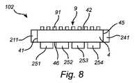
図3は、導光体4020の光出口面4200と光接続する光入力ファセット8060を備えた光学素子8010を含む導光体4020を示す。光学素子8010は、高い屈折率、一実施形態では導光体4020の屈折率以上の屈折率を有する材料からなり、四角形の断面並びに2つのテーパ状の側面8030及び8040を有する。テーパ状の側面8030及び8040は、導光体4020の光出口面4200から外側に傾き、光学素子8010の光出口ファセット8050は、光入力ファセット8060及び導光体4020の光出口面4200のどちらよりも大きな表面積を有する。あるいは、光学素子8010は3つ以上の、特に4つのテーパ状の側面を有してもよい。変形例では、光学素子8010は、円形の断面及び1つの円周状のテーパ状の側面を有する。このような構成によれば、光は傾斜面8030及び8040において反射され、光出口ファセット8050は光入力ファセット8060よりも大きいため、光が光出口ファセット8050に衝突した場合、脱出する可能性が高い。側面8030及び8040の形状は曲面でもよく、全ての光が光出口ファセット8050から出るよう選択され得る。 FIG. 3 shows a
また、光学素子は、例えば、導光体の一部を、所定の光学素子が導光体の端部のうちの1つに形成されるよう成形することにより、導光体4020から一体的に形成され得る。光学素子は、例えばコリメータの形状、又は台形の断面形状を有し、一実施形態では、台形の外面に反射層が設けられる。これにより、より大きなスポットサイズを有するよう受け取られた光を成形すると共に、光出口面以外の面を介する光の損失を最小化することにより、出射光の強度も高めることができる。他の実施形態では、光学素子はレンズアレイ、例えば凸レンズ、凹レンズ、又はこれらの組み合わせの形状を有する。これにより、焦点を合わせられた光、デフォーカスされた光、又はこれらの組み合わせを形成するよう、受け取られた光を成形することができる。レンズアレイの場合、更に、出射光は、アレイの1つ以上のレンズによってそれぞれ形成された2つ以上の別個のビームを有し得る。したがって、より一般的には、導光体は異なるサイズ及び異なる形状を有する部分を含み得る。これにより、極めて単純なやり方で、例えば光出口面のサイズ及び/又は形状を変更することによって、光出口面から任意の1つ以上の発光方向に光が成形され、光出口面から出射される光のビームサイズ及びビーム形状を調整可能な導光体が提供される。したがって、導光体の一部は光学素子として機能する。 Also, the optical element is integrally formed from the
また、光学素子は、導光体の光出口面に配置された集光素子(図示無し)であってもよい。集光素子は四角形の断面、及び、集光素子の光出口面が導光体の光出口面よりも大きい表面積を有するよう外側に曲がった2つの面を有する。あるいは、集光素子は、3つ以上の、具体的には4つのテーパ状の側面を有してもよい。集光素子は、放物線状の曲面を有する複合パラボラ集光素子(CPC)であってもよい。変形例では、集光素子は円形の断面及び1つの円周状のテーパ状の側面を有する。変形例において、集光素子の屈折率が導光体の屈折率よりも低く(しかし、空気の屈折率よりは高く)選択された場合、依然として相当な量の光を取り出すことができる。これは、高い屈折率を有する材料からなるものと比較して、製造が容易且つ安価な集光素子を可能にする。例えば、導光体がn=1.8の屈折率を有し、集光素子がn=1.5(ガラス)の屈折率を有する場合、係数2の光出力のゲインが達成され得る。n=1.8の屈折率の集光素子の場合、ゲインは更に約10%高くなる。実際には、光学素子又は集光素子と、一般的には空気である外部媒体との間の界面においてフレネル反射が存在するため、全ての光は取り出されない。これらのフレネル反射は、適切な反射防止コーティング、すなわち1/4λ誘電体多層膜又はモスアイ構造を使用することによって低減され得る。光出口ファセット上の位置に応じた光出力が不均一な場合、例えばコーティングの厚さを変えることによって、反射防止コーティングのカバレッジが変更され得る。 The optical element may be a light collecting element (not shown) disposed on the light exit surface of the light guide. The focusing element has a square cross-section and two faces bent outward such that the light exit face of the focusing element has a larger surface area than the light exit face of the light guide. Alternatively, the light collection element may have three or more, in particular four, tapered sides. The focusing element may be a compound parabolic focusing element (CPC) having a parabolic curved surface. In a variant, the light collecting element has a circular cross section and one circumferential tapered side. In an alternative embodiment, if the refractive index of the light collection element is selected to be lower than the refractive index of the light guide (but higher than the refractive index of air), still a significant amount of light can be extracted. This allows for a light-collecting element that is easy to manufacture and inexpensive compared to those made of materials with high refractive index. For example, if the light guide has a refractive index of n = 1.8 and the focusing element has a refractive index of n = 1.5 (glass), a gain of light output of
CPCの興味深い特徴の1つは、光のエタンデュ(=n2×面積×立体角(nは屈折率))が保存されることである。CPCの光入力ファセットの形状及びサイズは、導光体の光出口面の形状及びサイズに適合させることができ、この逆も成り立つ。CPCの大きな利点は、入射光の分布が、所与のアプリケーションの許容可能なエタンデュに最適に適合する光分布に変更されることである。CPCの光出口ファセットの形状は、適宜、例えば長方形又は円形等であり得る。例えば、デジタルプロジェクターの場合、ビームのサイズ(高さ及び幅)及び発散に対して要件が課される。対応するエタンデュがCPCにおいて保存される。この場合、使用されるディスプレイパネルの所望の高さ/幅の比を有する長方形の光入力及び出口ファセットを有するCPCを使用することは有益であろう。スポットライト用途の場合、要件はより緩和される。CPCの光出口ファセットは円形であってもよいが、特定の形状の領域を照らすために他の形状(例えば長方形)を有してもよく、又はスクリーン、壁、建物、インフラ等に所望のパターンを投射するためにかかるパターンを有してもよい。CPCは設計に大きな柔軟性を提供するが、その長さは比較的大きい可能性がある。一般的に、同じ性能を有するより短い光学素子を設計することが可能である。このために、表面形状及び/又は出口面は、例えば、光を集約するためにより湾曲した出口面を有するよう適合させられてもよい。1つの追加の利点は、CPCは、導光体のサイズがLEDの寸法によって制約され、光出口ファセットのサイズが後続の光学部品によって決定される場合に生じ得る縦横比のミスマッチを克服するために使用できることである。更に、例えば中心付近に又は中心に「穴」を有するミラーを使用して、CPCの光出口ファセットを部分的に覆うミラー(図示無し)を配置することができる。このようにすることで、CPCの出口面が狭められ、光の一部がCPC及び導光体内に反射し返され、光の出射エタンデュが低減される。当然ながら、これはCPC及び導光体から取り出される光の量を減らす。しかし、例えばAlanod 4200AGのように、このミラーが高い反射率を有する場合、光は実質的にCPC及び導光体に再投入され、TIRによって再循環され得る。これは光の角度分布を変えないが、再循環後、光がCPC出口面に衝突する位置を変え、よって、光束を増加させる。このようにすることで、通常はシステムのエタンデュを下げるために犠牲にされる光の部分を再取得し、例えば均一性を高めるために使用することができる。システムがデジタル投影アプリケーションに使用される場合、これは特に重要である。異なる態様でミラーを選択することにより、大量の光を犠牲にすることなく、異なるパネルサイズ及び縦横比を使用するシステムに対して同じCPC及び導光体のセットを使用することができる。このようにすることで、単一のシステムを様々なデジタル投影アプリケーションに使用することができる。One interesting CPC feature of the optical etendue (= n2 × area × solid angle (n is the refractive index)) is that is stored. The shape and size of the light input facets of the CPC can be adapted to the shape and size of the light exit face of the light guide, and vice versa. A major advantage of CPC is that the distribution of incident light is changed to a light distribution that best matches the allowable etendue of a given application. The shape of the light exit facets of the CPC may be, for example, rectangular or circular, as appropriate. For example, in the case of digital projectors, requirements are imposed on the beam size (height and width) and divergence. The corresponding etendue is stored at CPC. In this case, it would be beneficial to use a CPC with rectangular light input and output facets with the desired height / width ratio of the display panel used. For spotlight applications, the requirements are more relaxed. The light exit facets of the CPC may be circular, but may have other shapes (eg rectangular) to illuminate areas of particular shape, or the desired pattern for a screen, wall, building, infrastructure etc. May have such a pattern to project the While CPCs provide great flexibility in design, their length can be relatively large. In general, it is possible to design shorter optical elements with the same performance. To this end, the surface shape and / or the exit surface may, for example, be adapted to have a more curved exit surface to concentrate the light. One additional advantage is that CPC overcomes the aspect ratio mismatch that can occur if the light guide size is constrained by the dimensions of the LED and the light exit facet size is determined by the subsequent optics. It can be used. In addition, mirrors (not shown) that partially cover the light exit facets of the CPC can be arranged, for example using mirrors with “holes” near or at the center. In this way, the exit surface of the CPC is narrowed, part of the light is reflected back into the CPC and the light guide, and the outgoing etendue of the light is reduced. Of course, this reduces the amount of light extracted from the CPC and the light guide. However, if this mirror has high reflectivity, such as, for example,
図3を参照して説明された上記構造のうちのいずれかを使用することにより、屈折率が高い導光体材料から空気のような屈折率が低い物質に光を取り出すことに関する問題、特に取り出し効率に関する問題が解決される。 By using any of the above structures described with reference to FIG. 3, problems with extracting light from a high refractive index lightguide material to a low refractive index material such as air, in particular the extraction Problems with efficiency are solved.
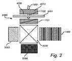
図2は、導光体4070を有する照明システム、例えばデジタルプロジェクターの側面図を示す。導光体4070は、出射光1700が黄色及び/又は橙色の波長範囲内、すなわち、約560nm〜600nmの波長範囲内になるよう入射光1300を変換するよう構成される。導光体4070は、例えば、Ceドープ(Lu,Gd)3Al5O12、(Y,Gd)3Al5O12、又は(Y,Tb)3Al5O12等のセラミック材料からなる透明なガーネットとして提供され得る。Ce含有量が多い場合、並びに/又は、例えばCeによるGd及び/若しくはTbの置換度が高い場合、導光体の発光のスペクトル分布はより高い波長にシフトし得る。一実施形態では、導光体4070は完全に透明である。FIG. 2 shows a side view of a lighting system, such as a digital projector, having a
光出口面4200には光学素子9090が設けられる。光学素子9090は、導光体4070から出射された光1700をフィルタリングしてフィルタリングされた光1701を提供するためのフィルタ9091、少なくとも1つの更なる光源9093、9094、及びフィルタリングされた光1701と少なくとも1つの更なる光源9093、9094からの光とを導出して共通の光出力1400を供給するよう構成された光学部品9092を含む。フィルタ9091は吸光フィルタ又は反射フィルタであり、固定又は切り替え可能であり得る。切り替え可能フィルタは、例えば、所望の光出力に応じてローパス、バンドパス、又はハイパスであり得る反射ダイクロイックミラー及び切り替え可能ミラーを設け、切り替え可能ミラーを光の進行方向で見てダイクロイックミラーの上流に配置することによって得ることができる。更に、2つ以上のフィルタ及び/又はミラーを組み合わせて、所望の光出力を選択することも可能である。図2に示されるフィルタ9091は、フィルタ9091の切り替え状態に応じて、フィルタリングされていない黄色及び/若しくは橙色光、又はフィルタリングされた光、具体的には、図示の実施形態ではフィルタリングされた赤色光を通過させることができる切り替え可能フィルタである。フィルタリングされた光のスペクトル分布は、採用されるフィルタ9091の特性に依存する。図示の光学部品9092は、Xキューブとも知られるクロスダイクロイックプリズムであってもよく、あるいは、個別のダイクロイックフィルタの適切なセットであってもよい。 An
図示の実施形態では、2つの更なる光源9093及び9094が設けられ、更なる光源9093は青色光源であり、更なる光源9094は緑色光源である。他の色の及び/又はより多くの更なる光源も実施可能である。更なる光源のうちの1つ以上は、後述される本発明の実施形態に係る導光体であってもよい。他のオプションは、フィルタ9091によって除去された光を更なる光源として使用することである。したがって、共通の光出力1400は、導光体4070によって出射され、フィルタ9091によってフィルタリングされた光1701と、2つの更なる光源9093及び9094によってそれぞれ出射された光との組み合わせである。共通の光出力1400は、好適には白色光であり得る。 In the illustrated embodiment, two
図2に示されるソリューションは、スケーラブルであり、費用対効果が高く、本発明の実施形態に係る発光素子の所与のアプリケーションの要件に応じて容易に適合可能であるという点で有利である。 The solution shown in FIG. 2 is advantageous in that it is scalable, cost effective, and easily adaptable to the requirements of a given application of light emitting devices according to embodiments of the present invention.
図3Aは、光ガイド4090Aの表面のうち光入力表面とは異なる1つの表面において、いくつかの実施形態ではそこから約30μm以下の距離のところに配置されたヒートシンク要素7000Aを備える光ガイド4090Aを示す側面図、図3Bは、光ガイド4090Bの表面のうち光入力表面とは異なる1つの表面において、いくつかの実施形態ではそこから約30μm以下の距離のところに配置されたヒートシンク要素7000Bを備える光ガイド4090Bを示す側面図である。実施形態に関係なく、ヒートシンク要素7000A、7000Bは、熱放散を改善するためのフィン7100、7200、7300を備えるが、これらのフィンは任意選択の要素である。実施形態に関係なく、ヒートシンク要素7000A、7000Bは、光ガイドの表面形状に沿うようになっており、したがって、光ガイドとの接触領域全体にわたって等角熱接触を実現するようになっている。これにより、熱接触面積の増大と、光ガイドの冷却の改善とが得られ、ヒートシンク要素の位置決めに関する既存の許容限界がそれほど重要ではなくなる。 FIG. 3A shows a
図3Aは、ヒートシンク要素7000Aが複数のヒートシンク部分、ここでは4つのヒートシンク部分7001、7002、7003及び7004を備え、そのうちの1つ又は複数、ここでは4つ全てが、フィンを備えることができることを示している。ヒートシンク要素7000Aが備えるヒートシンク部分が増えるほど、より精密にヒートシンク要素7000Aを光ガイドの表面に沿わせることができる。各ヒートシンク部分7001、7002、7003及び7004は、光ガイドとの接触領域全体にわたって等角熱接触を実現するようになっている。これらのヒートシンク部分は、光ガイドの表面から互いに異なる距離のところに配置することができる。さらに、ヒートシンク要素7000Aは、ヒートシンク部分7001、7002、7003及び7004がそれぞれ取付け要素7010、7020、7030及び7040によって個々に取り付けられる共通担体7050を備える。或いは、各ヒートシンク部分に、それ自体の担体を割り当てることもできる。これらの要素は、任意選択であることに留意されたい。 FIG. 3A shows that the
図3Bは、ヒートシンク要素7000Bが、それが配置されることになる光ガイド4090Bの表面の形状に沿うことができるように構成された底部7060を備えることを示している。底部7060は、可撓性であり、例えば銅層など、熱伝導性金属層とすることができる。ヒートシンク要素7000Bは、ヒートシンク要素7000Bの可撓性及び形状順応性を改善するために底部要素7060とヒートシンク要素7000Bの残りの部分との間に配置された熱伝導性層7070をさらに備える。熱伝導性層7070は、例えば、熱伝導性流体又はペーストとすることができる。熱伝導性層7070は、一実施形態では、反射性が高く、かつ/又は反射性の高いコーティングを備える。ヒートシンク要素7000Bは、熱放散を改善するための流体流を生成するためのヒートシンク要素7000Bの内部に配置された流体溜め7080をさらに備える。代替形態では、流体溜め7080は、ヒートシンク要素7000Bの外側に、例えばヒートシンク要素7000Bの外周の一部又は全体に沿って延びるように配置することもできる。流体流は、ポンプによって増強することもできる。熱伝導性層7070及び流体溜め7080は任意選択の要素であることに留意されたい。 FIG. 3B shows that the heat sink element 7000B comprises a bottom 7060 configured to be able to conform to the shape of the surface of the light guide 4090B in which it is to be placed.
実施形態に関係なく、ヒートシンク要素7000A、7000Bは、銅、アルミニウム、銀、金、炭化ケイ素、窒化アルミニウム、窒化ホウ素、アルミニウムケイ素炭化物、酸化ベリリウム、シリコン/炭化ケイ素、アルミニウムケイ素炭化物、銅タングステン合金、銅モリブデン炭化物、炭素、ダイヤモンド、グラファイト、及びそれらの2つ以上の組合せから選択した材料で構成することができる。さらに、上述の実施形態の特徴を併せ持つヒートシンク要素も可能である。また、上記の実施形態のいずれかによるヒートシンク要素を、光ガイド4090A又は4090Bの複数の表面に配置することも可能である。 Regardless of the embodiment, the
最後に、ヒートシンク要素を上述のように設けることは、赤波長範囲で放射する、かつ/又は例えばIR発光蛍光体を備えることによって赤外波長範囲で光を放射するようになされている光源を利用する発光デバイスで特に有利であることに留意されたい。 Finally, providing the heat sink element as described above utilizes a light source adapted to emit light in the infrared wavelength range by emitting in the red wavelength range and / or for example by providing an IR emitting phosphor Note that it is particularly advantageous for light emitting devices that
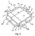
図4は、本発明の第1の一般的な実施形態による発光デバイス1を示す斜視図である。図5は、図4の発光デバイス1を示す上面図である。発光デバイス1は、一般に、少なくとも1つのLED又はレーザダイオードなどの固体状態光源をそれぞれ備える複数の光源211、212、221、222、231、232、241及び242と、少なくとも1つの光入力側面41及び光出力表面42を有する光ガイド4とを備える。適当なタイプのLED又はレーザダイオードについては、上述した。 FIG. 4 is a perspective view of a
光ガイド4は、4つの光入力側面、すなわち第1、第2、第3及び第4の光入力表面41、43、44及び45と、光ガイド4の上面となるように、4つの光入力側面41、43、44及び45のそれぞれに対して0°以外の角度をなして延びる光出口表面42とを有する正方形プレートとして概ね成形されるものとして示してある。光ガイド4は、光出口表面42と対向してこれと平行に延びる底面46をさらに備える。 The
光入力側面41と光出口表面42との間の角度が90°未満である実施形態も、90°に等しい実施形態も、90°より大きい実施形態も、全て可能であることに留意されたい。 It should be noted that both embodiments where the angle between the
この実施形態では、4つの光入力側面41、43、44及び45はそれぞれ2つの光源と関連付けられ、第1の光入力側面41が光源211及び212と関連付けられ、第2の光入力側面43が光源231及び232と関連付けられ、第3の光入力側面44が光源221及び222と関連付けられ、第4の光力側面45が光源241及び242と関連付けられている。各光源は、光ガイド4の関連する光入力側面に隣接して、光学接触するように配置される。 In this embodiment, the four light input sides 41, 43, 44 and 45 are each associated with two light sources, the first
代替の実施形態では、各光入力表面は、原理的には、任意のその他の数の光源と、又は光源のアレイとも、関連付けることができる。また、各光入力表面は、必ずしも同数の光源と関連付ける必要があるわけではなく、1つ又は複数の異なる数の光源と関連付けることができる。 In alternative embodiments, each light input surface can in principle be associated with any other number of light sources, or with an array of light sources. Also, each light input surface need not necessarily be associated with the same number of light sources, but can be associated with one or more different numbers of light sources.
代替の実施形態では、光ガイドの幾何学的形状に応じて、光ガイド4は、4つ以外の数の光入力側面、例えば3つ、5つ、又はそれよりさらに多くの光入力側面を備えることができる。 In an alternative embodiment, depending on the geometry of the light guide, the
いかなる光源とも関連付けられず、したがって光入力表面として使用されない、光出口表面42以外の光ガイド4の表面は、例えば普通ならそれらの表面を通して発生する可能性がある光損失を解消するように反射層を備え、かつ/又はヒートシンクを備えることができる。 The surfaces of the
光ガイド4は、バー又はロッド形状にすることもでき、或いは長方形プレートの形状にすることもできる。さらに、光ガイド4は、原理的には、これらに限定されるわけではないが、三角形、長方形、正方形、台形、多角形及びそれらの組合せなど、任意の実現可能な断面形状を有することができる。 The
光出口表面42と表面46とが互いに対向する側面であり、光入力側面41が上面又は底面であるような本発明による発光デバイスの代替の構成も、可能である。 Alternative configurations of the light emitting device according to the invention are also possible, such that the
さらに、光ガイド4は、透明材料、ルミネセンス材料、ガーネット、集光材料又はそれらの組合せを含み、適当な材料及びガーネットについては上述した。例えば、光ガイドは、少なくとも50%、少なくとも60%及び少なくとも70%のうちのいずれか1つの透明度を有する材料を含むことがある。ただし、好ましくは、あるスペクトル分布を有する光を別のスペクトル分布を有する光に変換するように構成された材料を含む透明な光ガイドである。あるスペクトル分布を有する光を別のスペクトル分布を有する光に変換するように構成された材料は、光ガイド4の表面に配置してもよいし、或いは光ガイド4に埋め込む、又は内蔵してもよい。 Furthermore, the
光源211、212、221、222、231、232、241、242は、例えば光学接着剤によって、それぞれ第1、第2、第3及び第4の光入力側面41、43、44、45上に直接配置される。他の実施形態(例えば図10参照)では、光源は、基材又は基板151、152、153、154上に配置されることがある。基材又は基板151、152、153、154は、好ましくは銅、鉄又はアルミニウムなどの金属で構成されたヒートシンクの形態で設けることができる。ヒートシンクは、熱放散を改善するためのフィン(図示せず)を備えることができる。他の実施形態では、基材又は基板は、ヒートシンクでなくてもよいことに留意されたい。また、基材又は基板は不可欠なものではないので、さらに他の実施形態では省略されることもある。 The
次に図6及び図7を参照すると、図4に示す互いに直交する2つの方向XI−XI及びXII−XIIから見た、図4の発光デバイスの断面図が示してある。 6 and 7, there is shown a cross-sectional view of the light emitting device of FIG. 4 as viewed from the two mutually orthogonal directions XI-XI and XII-XII shown in FIG.
図6及び図7の両図で分かるように、4つの追加の光源251、252、253及び254が、底面46上に配置され、これと光学接続している。底面と関連付けられた4つの追加の光源251、252、253及び254のうち3つ、すなわち追加の光源251、252及び253は、これらの図面で見えている。したがって、底面46は、この図示の実施形態では、光出口表面42と平行に延びる光入力表面である。 As can be seen in both FIGS. 6 and 7, four additional
光出口表面42は、さらに、面積A及び周囲長Cを有し、光入力側面は、光出口表面42が延びる平面に対して0°以外の角度で、特に直交するように延びる高さHiを有する。光出口表面42の周囲長Cは、高さHiの4倍超になるような大きさにされる。The
一般に、光入力側面の面積は、光出口表面の面積Aの4倍未満になるような大きさにされる。光ガイド4が4つの光入力側面41、42、43、44を備える図示の実施形態では、第1、第2、第3及び第4の光入力側面41、42、43及び44の面積の和、換言すれば総面積が、光出口表面42の面積Aの4倍未満になるような大きさにされる。特に、光ガイド4は、光出口表面の面積Aが100mm2未満かつ0.25mm2超となるように、かつ高さHiが10mm未満かつ0.5mm超となるような寸法とされる。Generally, the area of the light input side is sized to be less than four times the area A of the light exit surface. In the illustrated embodiment in which the
光ガイド4は、さらに、長さL、幅W及び高さHを有する。さらに詳細には、光ガイド4は、長さLと幅Wとが、光出口表面42の平面である共通の平面内で互いに直交して延び、高さHが、光入力側面の高さHiと同じ高さ、換言すれば等しい高さであり、かつ光ガイド4の幅W及び長さLの両方に対して概ね0°以外の角度で延びる、図4〜図7に示す実施形態ではそれらに直交して延びるように、構成される。The
図6及び図7から明らかなように、光ガイド4は、高さHが長さL及び幅Wの両方より小さくなるように構成される。好ましくは、光ガイド4は、高さHが0.5mmから10mmの範囲に含まれ、長さLが2mmから25mmの範囲に含まれ、かつ/又は幅Wが2mmから25mmの範囲に含まれるように構成される。いくつかの実施形態では、長さL、幅W及び高さHは全て、それぞれ上述の範囲に収まる寸法を有する。 As apparent from FIGS. 6 and 7, the
図示の実施形態では、4つの光入力側面41、43、44、45は全て、各光入力側面の長手方向に一定の同じ高さを有する。代替の実施形態では、光入力側面41、43、44、45は、2種類以上の互いに異なる高さを有することがあるが、好ましくは、その全てが0.5mmから10mmの範囲に収まる寸法であり、各光入力側面の高さは、やはり各光入力側面の長手方向に一定である。光入力側面41、43、44、45が2種類以上の互いに異なる高さを有する代替の実施形態では、光ガイドは、光入力側面のうちの少なくとも1つの高さ、好ましくは光入力側面のうちのそれ以上又は全ての高さが、長さL及び幅Wより小さくなるように構成される。さらに他の代替の、又は追加の実施形態では、光入力側面のうちの1つ又は複数の高さは、各光入力側面の長手方向に変化することがあるが、それでも常に0.5mmから10mmの範囲内に収まることが好ましい。 In the illustrated embodiment, all four light input sides 41, 43, 44, 45 have the same height in the longitudinal direction of each light input side. In alternative embodiments, the light input sides 41, 43, 44, 45 may have two or more different heights, but preferably all of which are sized to fit within the range of 0.5 mm to 10 mm. The height of each light input side is also constant in the longitudinal direction of each light input side. In an alternative embodiment in which the light input sides 41, 43, 44, 45 have two or more different heights, the light guide comprises at least one height of the light input sides, preferably of the light input sides. Are configured such that the height of all or more of them is smaller than the length L and the width W. In still other alternative or additional embodiments, the height of one or more of the light input sides may vary along the length of each light input side, but still always 0.5 mm to 10 mm It is preferable to fall within the range of
図6を参照すると、本発明による発光デバイスは、概略的には以下のように動作する。第1のスペクトル分布を有する光13が、少なくとも1つの光源211、212、221、222、231、232、241及び242のそれぞれと、追加の光源251、252、253及び254のそれぞれとによって放射される。211で示される光源から放射される光によって例示されるように、第1のスペクトル分布を有する光13は、次いで、第1の光入力側面41で光ガイド4に導入される。第1のスペクトル分布を有する光13の少なくとも一部分は、光ガイド4によって、第2のスペクトル分布を有する光14に変換される。第2のスペクトル分布を有する光14は、次いで、光出口表面42で光ガイド4の外部に導出され、したがって発光デバイス1から放射される。 Referring to FIG. 6, the light emitting device according to the present invention operates generally as follows. A light 13 having a first spectral distribution is emitted by each of the at least one
好ましくは、実施形態に関係なく、第1のスペクトル分布、すなわち光源から放射される光のスペクトル分布は、200nmから500nmの範囲に含まれ、第2のスペクトル分布は、400nmから800nmの範囲に含まれる。これにより、高品質及び高強度の白色光出力を提供するのに特に適した発光デバイスが提供される。 Preferably, regardless of the embodiment, the first spectral distribution, ie the spectral distribution of the light emitted from the light source is comprised in the range of 200 nm to 500 nm and the second spectral distribution is comprised in the range of 400 nm to 800 nm Be This provides a light emitting device particularly suitable for providing high quality and high intensity white light output.
図示の実施形態では、全ての光源が、実質的に同じスペクトル分布を有する光を放射する。ただし、代替の実施形態では、これらの光源が2種類以上の異なるスペクトル分布を有する光を放射することも可能である。 In the illustrated embodiment, all light sources emit light having substantially the same spectral distribution. However, in alternative embodiments, it is possible that these light sources emit light having two or more different spectral distributions.
実施形態に関係なく、第1のスペクトル分布を有する光13と第2のスペクトル分布を有する光14とが、同じスペクトル分布、又は実質的に完全に重複するスペクトル分布を有することができる。或いは、やはり実施形態に関係なく、第1のスペクトル分布を有する光13と第2のスペクトル分布を有する光14とが、異なるスペクトル分布、例えば部分的にしか重複しない、又は実質的に重複しないスペクトル分布を有することもある。 Regardless of the embodiment, the light 13 having the first spectral distribution and the light 14 having the second spectral distribution can have the same spectral distribution, or a spectral distribution that substantially completely overlaps. Alternatively, again regardless of the embodiment, the light 13 having the first spectral distribution and the light 14 having the second spectral distribution have different spectral distributions, eg spectra that only partially overlap or do not substantially overlap. It may also have a distribution.
いくつかの実施形態(図示せず)では、発光デバイスは、例えば光ガイドの側面上に配置された好ましくは銅、鉄又はアルミニウムなどの金属で構成されたヒートシンクをさらに備える。ヒートシンクは、熱放散を改善するためのフィンを備える。光源が載置される基材又は基板を備える他の実施形態(例えば図10参照)では、基材又は基板がヒートシンクとして機能していることもあることに留意されたい。ヒートシンクを設けることによって、光源によって生成される熱を、光ガイドから効率的に放散させることができる。これにより、発光デバイスの得られる最大出力光強度の上昇、並びに光ガイド中の過剰な熱によって引き起こされる発光デバイスの光学的性能への悪影響の低減又は解消が得られる。ただし、ヒートシンクは不可欠な要素ではなく、したがって、さらに他の実施形態では省略されることもある。 In some embodiments (not shown), the light emitting device further comprises a heat sink, for example preferably made of metal such as copper, iron or aluminum, arranged on the side of the light guide. The heat sink comprises fins for improving the heat dissipation. It should be noted that in other embodiments comprising a substrate or substrate on which the light source is mounted (see, for example, FIG. 10), the substrate or substrate may function as a heat sink. By providing a heat sink, the heat generated by the light source can be efficiently dissipated from the light guide. This results in an increase in the maximum achievable output light intensity of the light emitting device as well as a reduction or elimination of an adverse effect on the optical performance of the light emitting device caused by excessive heat in the light guide. However, the heat sink is not an essential element, and may therefore be omitted in further embodiments.
図8は、図6及び図7の発光デバイスと同様の本発明による発光デバイス102の第3の実施形態を示す側面図である。この実施形態では、光ガイド4の光入力底面46は、4つの光源251〜254と関連付けられる。光ガイド4は、光出口表面42に配置された反射偏光子91の形態の、光ガイド4から外部に光を導出する導出構造9をさらに備える。したがって、この実施形態では、発光デバイスは、偏光を放射するようになされている。 FIG. 8 is a side view of a third embodiment of a
図9は、図8の発光デバイスと同様の本発明による発光デバイス103の第4の実施形態を示す側面図である。この実施形態では、光ガイド4の光入力底面46は、4つの光源251〜254と関連付けられる。光ガイド4は、光出口表面42に配置された輝度向上フィルム(BEF)構造92の形態の、光ガイド4から外部に光を導出する導出構造9をさらに備える。この実施形態では、BEF構造により、平行光を放射するように構成された発光デバイス1が得られる。 FIG. 9 is a side view showing a fourth embodiment of a
代替の実施形態では、光ガイド4から外部に光を導出する導出構造9は、格子又はフォトニック結晶とすることができ、かつ/或いは光出口表面42内に成形する、又は埋め込むことができる。光ガイド4から外部に光を導出する導出構造9及びヒートシンクの両方を備えるさらに他の実施形態では、導出構造とヒートシンクとが互いに熱接触して配置されることもある。 In an alternative embodiment, the outcoupling structure 9 for extracting light out of the
以下、図10及び図11を参照して、本発明を例示する実施例について述べる。 Hereinafter, with reference to FIG. 10 and FIG. 11, the example which illustrates this invention is described.
実施例1
実験において、図10に示す本発明の第5の実施形態による発光デバイス104を調査した。この実施形態では、発光デバイス104は、光ガイド4と、それぞれ基材151、152、153及び154上に配置された4つの光源21、22、23及び24とを備える。ここで行った実験では、光ガイド4の(垂直)側面には光源を配置せず、その代わりにこのような実施形態は、以下でさらに述べる計算の対象とした。Example 1
In an experiment, a
光源21、22、23及び24は、1.4×1.4mm2のサイズを有し、波長450nmの光を放射する、高出力のLUMILEDS(LUMILED)社製DOSC LEDである。光ガイド4は、青色光を緑色光に変換するように構成された3×4mm2(長さL×幅W)の光出口表面積を有する蛍光体ドープYAG:Ceプレートの形態で設けられる。光ガイド4は、透明シリコーン接着剤によって、光源21、22、23及び24の上部に接着される。The
光出力は、1A、1.4A及び2Aの連続電流で測定した。その結果を、表2に示す。使用したDOSC LEDは、1Aで動作するように指定されているが、自動車の応用分野では、これらのLEDは、1.4Aで動作する。1.4Aでは、ルーメン光出力は、光ガイド4の上面から抽出された光について1165Lmと測定された。 The light output was measured at continuous currents of 1A, 1.4A and 2A. The results are shown in Table 2. The DOSC LEDs used are specified to operate at 1A, but in automotive applications these LEDs operate at 1.4A. At 1.4 A, the lumen light output was measured at 1165 Lm for light extracted from the top surface of the
薄い高濃度蛍光体ドープYAG:Ceプレートでは、ルーメン光出力は、原理的には、上面及び(垂直)側面の両方から光を抽出したときに、1665Lmと高くなる可能性もあることに留意されたい。ただし、以下の表から明らかであるように、ルーメン光出力は、本発明で提示しているように側面を光入力表面として使用することにより、さらに高くなることもある。
様々な数の光源についての予想ルーメン光出力を計算するために、図10に示す実施形態の発光デバイス104に基づいて、解析用光リサイクルモデルを作成した。光ガイド4の底面に4つの光源21、22、23及び24だけが光学的に接着されている場合には、光ガイド4の厚さは、ゼロに近い。この場合には、ルーメン光出力は、上記で示したように、1665Lmに近い。解析モデルで使用する際には、この値を1に正規化した。 A light recycling model for analysis was created based on the
光源の数と光出力の利得との間の関係を、図11に示す。この関係は、図示のように、対数関数である。計算のために、2つの光源(図示せず)を、光ガイド4の各(垂直)側面に追加する。光ガイド4の高さHは、単一の光源の長さ及び幅と同じ、すなわち1.4mmであり、高さHが、光ガイド4の上面の長さL(3mm)及び幅W(4mm)の両方より小さくなるようになっている。この場合には、発光デバイス104は、合計で4+4×2=12個の光源を備える。解析用光リサイクルモデルを用いて、光ガイドの上面からの正規化ルーメン光出力は、図11のグラフに示すように2となるものと計算される。これは、2倍の光出力である3330Lmに相当する。 The relationship between the number of light sources and the gain of the light output is shown in FIG. This relationship is logarithmic as shown. Two light sources (not shown) are added to each (vertical) side of the
底部に4個、4つの側面に4×4個で、合計20個の光源を備える実施形態では、正規化光出力は2.5であり、これは4163Lmのルーメン光出力に相当する。これは、例えばデジタル投影では、依然として実際的かつ興味深い解決策である。 In the embodiment with 20 light sources in total, with 4 at the bottom and 4 × 4 on 4 sides, the normalized light output is 2.5, which corresponds to a lumen light output of 4163 Lm. This is still a practical and interesting solution, for example in digital projection.
底部に9個、4つの側面に4×9個で、合計45個の光源を備える実施形態であれば、ルーメン光出力は、9367Lmとなる。 For an embodiment with ninety at the bottom and four by nine on four sides, for a total of 45 light sources, the lumen light output would be 9367 Lm.
底部に4個、4つの側面に4×6個で、合計28個の光源を備える実施形態では、正規化光出力は2.75であり、これは4579Lmのルーメン光出力に相当する。 In the embodiment with 28 light sources in total, 4 x 6 at the bottom and 4 x 6 on 4 sides, the normalized light output is 2.75, which corresponds to a lumen light output of 4579 Lm.
したがって、余分の光源の良い効果は、最初は非常に大きいが、その後次々に小さくなり、光源を追加する際の投資に対して得られる利得は小さくなる。全体的な効率は、多数の光源を適用したときには小さくなる。相対的に大きくなる光源によって生成される熱を冷却しなければならないからである。 Thus, the good effect of the extra light source is initially very large, but then one after the other, and the gain obtained for the investment in adding the light source is small. The overall efficiency is reduced when applying multiple light sources. This is because the heat generated by the relatively large light source must be cooled.
当業者なら、本発明が上述の好ましい実施形態に限定されないことを理解するであろう。限定されるどころか、添付の特許請求の範囲内で、多数の修正及び変形が可能である。 Those skilled in the art will appreciate that the present invention is not limited to the preferred embodiments described above. Numerous modifications and variations are possible, not limiting, within the scope of the appended claims.
さらに、図面、開示及び添付の特許請求の範囲を検討することにより、当業者なら、請求する発明を実施する際に、開示した実施形態の変形を理解し、実施することができる。特許請求の範囲において、「備える」という言葉は、その他の要素又はステップを排除するものではなく、不定冠詞「a」及び「an」は、複数を排除するものではない。特定の手段が互いに異なる従属請求項に記載されていても、その事実のみを以て、それらの手段を組み合わせて有利に使用することができないということにはならない。 Furthermore, upon reviewing the drawings, the disclosure and the appended claims, those of ordinary skill in the art will be able, when practicing the claimed invention, to understand and practice variations of the disclosed embodiments. In the claims, the word "comprising" does not exclude other elements or steps, and the indefinite articles "a" and "an" do not exclude a plurality. The mere fact that certain measures are recited in mutually different dependent claims does not indicate that a combination of these measures can not be used to advantage.
Claims (14)
Translated fromJapanese光出口表面及び少なくとも3つの光入力側面を備える光ガイドであって、前記光出口表面及び少なくとも3つの前記光入力側面が、互いに対して0°以外の角度で延びる光ガイドと、
を備える発光デバイスであって、
前記光ガイドは、前記複数の光源からの前記第1のスペクトル分布を持つ光を少なくとも3つの前記光入力側面のそれぞれで受光し、光を前記光出口表面まで案内し、前記第1のスペクトル分布を持つ光の少なくとも一部分を第2のスペクトル分布を持つ光に変換し、前記第2のスペクトル分布を持つ光の少なくとも一部分を前記光出口表面から外部に導出し、
前記光出口表面は、面積A及び周囲長Cを持ち、
少なくとも3つの前記光入力側面は、前記光出口表面が延びる平面に対して0°以外の角度で伸びる高さHiを持ち、
前記光出口表面の前記周囲長Cは、少なくとも3つの前記光入力側面の前記高さHiの4倍超であり、少なくとも3つの前記光入力側面の総面積は、前記光出口表面の前記面積Aの4倍未満であり、
前記光出口表面の前記面積Aは、100mm2未満且つ0.25mm2超である、発光デバイス。A plurality of light sources emitting light having a first spectral distribution during operation;
A light guide comprising a light exit surface and at least three light input sides, the light exit surface and the at least three light input sides extending at an angle other than 0 ° with respect to each other;
A light emitting device comprising
The light guide receives light having the first spectral distribution from the plurality of light sources at each of at least three of the light input side surfaces and guides light to the light exit surface, the first spectral distribution Converting at least a portion of the light having a second spectral distribution to light having at least a portion of the light having the second spectral distribution out of the light exit surface;
The light exit surface has an area A and a perimeter C,
At least three of the light input sides have a height Hi extending at an angle other than 0 ° with respect to the plane in which the light exit surface extends,
The perimeter C of the light exit surface is more than four times the height Hi of the at least three light input sides, and the total area of the at least three light input sides is the area of the light exit surface 4 times less than der of ais,
The area A of the light exit surface, Ru100 mm2and less than 0.25 mm2Ultra der light emitting device.
前記光ガイドは、前記光出口表面と平行に延びる光入力底面をさらに備え、
前記光ガイドは、前記少なくとも1つの追加の光源からの前記第1のスペクトル分布を持つ光を少なくとも1つの前記光入力底面で受光し、前記第1のスペクトル分布を持つ光を前記光出口表面まで案内し、前記第1のスペクトル分布を持つ光の少なくとも一部分を前記第2のスペクトル分布を持つ光に変換し、前記第2のスペクトル分布を持つ光の少なくとも一部分を前記光出口表面から外部に導出する、請求項1乃至3の何れか一項に記載の発光デバイス。The light emitting device further comprises at least one additional light source which emits light having the first spectral distribution in operation,
The light guide further comprises a light input bottom extending parallel to the light exit surface,
The light guide receives light having the first spectral distribution from the at least one additional light source at at least one light input bottom, and light having the first spectral distribution to the light exit surface Guiding and converting at least a portion of the light having the first spectral distribution into light having the second spectral distribution and directing at least a portion of the light having the second spectral distribution to the outside from the light exit surface The light emitting device according to any one of claims 1 to 3.
Applications Claiming Priority (1)
| Application Number | Priority Date | Filing Date | Title |
|---|---|---|---|
| PCT/EP2014/074949WO2016078700A1 (en) | 2014-11-19 | 2014-11-19 | A light emitting device |
Publications (2)
| Publication Number | Publication Date |
|---|---|
| JP2018503211A JP2018503211A (en) | 2018-02-01 |
| JP6501370B2true JP6501370B2 (en) | 2019-04-17 |
Family
ID=51905085
Family Applications (1)
| Application Number | Title | Priority Date | Filing Date |
|---|---|---|---|
| JP2017526636AActiveJP6501370B2 (en) | 2014-11-19 | 2014-11-19 | Light emitting device |
Country Status (5)
| Country | Link |
|---|---|
| US (1) | US20170307798A1 (en) |
| EP (1) | EP3221637B1 (en) |
| JP (1) | JP6501370B2 (en) |
| CN (1) | CN106922178B (en) |
| WO (1) | WO2016078700A1 (en) |
Families Citing this family (3)
| Publication number | Priority date | Publication date | Assignee | Title |
|---|---|---|---|---|
| US11256019B2 (en)* | 2019-06-14 | 2022-02-22 | Wuhan China Star Optoelectronics Technology Co., Ltd. | Backlight module and display device |
| CN111193914A (en)* | 2020-01-10 | 2020-05-22 | 厦门卓旭智能科技有限公司 | Projector convenient to calibration projection position and good stability |
| CN113363368B (en)* | 2021-05-19 | 2022-05-10 | 厦门镌纹科技有限公司 | Two-dimensional period asymmetric grating optical device and electronic equipment |
Family Cites Families (9)
| Publication number | Priority date | Publication date | Assignee | Title |
|---|---|---|---|---|
| US5667289A (en)* | 1989-05-18 | 1997-09-16 | Seiko Epson Corporation | Background lighting apparatus for liquid crystal display |
| JP2002350846A (en)* | 2001-05-22 | 2002-12-04 | Yazaki Corp | LED backlight |
| US7316497B2 (en)* | 2005-03-29 | 2008-01-08 | 3M Innovative Properties Company | Fluorescent volume light source |
| JP2008305713A (en)* | 2007-06-08 | 2008-12-18 | Fujifilm Corp | Surface lighting device |
| JP2009123553A (en)* | 2007-11-15 | 2009-06-04 | Sumitomo Chemical Co Ltd | Light guide plate, surface light source device, and liquid crystal display device |
| JP2012043617A (en)* | 2010-08-18 | 2012-03-01 | Fujifilm Corp | Planar lighting device |
| EP2447746A1 (en) | 2010-10-28 | 2012-05-02 | Koninklijke Philips Electronics N.V. | Lighting device with waveguide plate |
| CN103314254A (en)* | 2010-12-02 | 2013-09-18 | 英特曼帝克司公司 | Solid-state lamps with light guide and photoluminescence material |
| US9170351B2 (en)* | 2011-06-17 | 2015-10-27 | Nec Corporation | Optical element, light source apparatus, and projection-type display apparatus |
- 2014
- 2014-11-19WOPCT/EP2014/074949patent/WO2016078700A1/enactiveApplication Filing
- 2014-11-19USUS15/521,315patent/US20170307798A1/ennot_activeAbandoned
- 2014-11-19CNCN201480083451.4Apatent/CN106922178B/enactiveActive
- 2014-11-19EPEP14799776.1Apatent/EP3221637B1/enactiveActive
- 2014-11-19JPJP2017526636Apatent/JP6501370B2/enactiveActive
Also Published As
| Publication number | Publication date |
|---|---|
| CN106922178B (en) | 2020-01-31 |
| WO2016078700A1 (en) | 2016-05-26 |
| JP2018503211A (en) | 2018-02-01 |
| EP3221637A1 (en) | 2017-09-27 |
| EP3221637B1 (en) | 2018-05-23 |
| CN106922178A (en) | 2017-07-04 |
| US20170307798A1 (en) | 2017-10-26 |
Similar Documents
| Publication | Publication Date | Title |
|---|---|---|
| JP6173609B2 (en) | Light emitting element | |
| JP6000480B2 (en) | Light emitting element | |
| JP5985091B1 (en) | Light emitting element | |
| JP6165361B2 (en) | Light emitting device | |
| US9462650B2 (en) | Light emitting device and a method for dimming a light emitting device | |
| US20160218260A1 (en) | A light emitting device | |
| JP6466467B2 (en) | Light emitting device with spectral conversion element | |
| JP2016531385A5 (en) | ||
| JP6603220B2 (en) | Light emitting device | |
| JP6501370B2 (en) | Light emitting device |
Legal Events
| Date | Code | Title | Description |
|---|---|---|---|
| A521 | Request for written amendment filed | Free format text:JAPANESE INTERMEDIATE CODE: A523 Effective date:20171115 | |
| A621 | Written request for application examination | Free format text:JAPANESE INTERMEDIATE CODE: A621 Effective date:20171115 | |
| A977 | Report on retrieval | Free format text:JAPANESE INTERMEDIATE CODE: A971007 Effective date:20180706 | |
| A131 | Notification of reasons for refusal | Free format text:JAPANESE INTERMEDIATE CODE: A131 Effective date:20180717 | |
| RD02 | Notification of acceptance of power of attorney | Free format text:JAPANESE INTERMEDIATE CODE: A7422 Effective date:20180724 | |
| RD04 | Notification of resignation of power of attorney | Free format text:JAPANESE INTERMEDIATE CODE: A7424 Effective date:20180801 | |
| TRDD | Decision of grant or rejection written | ||
| A01 | Written decision to grant a patent or to grant a registration (utility model) | Free format text:JAPANESE INTERMEDIATE CODE: A01 Effective date:20190221 | |
| A61 | First payment of annual fees (during grant procedure) | Free format text:JAPANESE INTERMEDIATE CODE: A61 Effective date:20190315 | |
| R150 | Certificate of patent or registration of utility model | Ref document number:6501370 Country of ref document:JP Free format text:JAPANESE INTERMEDIATE CODE: R150 | |
| R250 | Receipt of annual fees | Free format text:JAPANESE INTERMEDIATE CODE: R250 | |
| R250 | Receipt of annual fees | Free format text:JAPANESE INTERMEDIATE CODE: R250 | |
| R250 | Receipt of annual fees | Free format text:JAPANESE INTERMEDIATE CODE: R250 | |
| R250 | Receipt of annual fees | Free format text:JAPANESE INTERMEDIATE CODE: R250 |