JP6500700B2 - Integrated substrate for resistive elements - Google Patents
Integrated substrate for resistive elementsDownload PDFInfo
- Publication number
- JP6500700B2 JP6500700B2JP2015166914AJP2015166914AJP6500700B2JP 6500700 B2JP6500700 B2JP 6500700B2JP 2015166914 AJP2015166914 AJP 2015166914AJP 2015166914 AJP2015166914 AJP 2015166914AJP 6500700 B2JP6500700 B2JP 6500700B2
- Authority
- JP
- Japan
- Prior art keywords
- conductor
- conductive patterns
- region
- terminal portion
- electrode
- Prior art date
- Legal status (The legal status is an assumption and is not a legal conclusion. Google has not performed a legal analysis and makes no representation as to the accuracy of the status listed.)
- Active
Links
- 239000000758substrateSubstances0.000titleclaimsdescription104
- 230000001681protective effectEffects0.000claimsdescription35
- 238000005520cutting processMethods0.000claimsdescription9
- 239000011159matrix materialSubstances0.000claimsdescription5
- 238000002679ablationMethods0.000claimsdescription4
- 239000004020conductorSubstances0.000description330
- 239000010410layerSubstances0.000description90
- 239000010408filmSubstances0.000description45
- 239000003990capacitorSubstances0.000description40
- 239000002131composite materialSubstances0.000description33
- 238000000034methodMethods0.000description26
- 239000000919ceramicSubstances0.000description22
- 239000000463materialSubstances0.000description17
- 238000007747platingMethods0.000description17
- 229910052751metalInorganic materials0.000description11
- 239000002184metalSubstances0.000description11
- 239000010409thin filmSubstances0.000description7
- 238000004519manufacturing processMethods0.000description6
- 239000011347resinSubstances0.000description6
- 229920005989resinPolymers0.000description6
- 239000011521glassSubstances0.000description5
- 229910052802copperInorganic materials0.000description4
- 229910052759nickelInorganic materials0.000description4
- 230000000149penetrating effectEffects0.000description4
- 239000000523sampleSubstances0.000description4
- 238000007650screen-printingMethods0.000description4
- 229910052709silverInorganic materials0.000description4
- 238000009966trimmingMethods0.000description4
- 229910001252Pd alloyInorganic materials0.000description2
- PNEYBMLMFCGWSK-UHFFFAOYSA-Naluminium oxideInorganic materials[O-2].[O-2].[O-2].[Al+3].[Al+3]PNEYBMLMFCGWSK-UHFFFAOYSA-N0.000description2
- 230000015572biosynthetic processEffects0.000description2
- 229910010293ceramic materialInorganic materials0.000description2
- 230000000694effectsEffects0.000description2
- 239000003822epoxy resinSubstances0.000description2
- 238000007646gravure printingMethods0.000description2
- 229910010272inorganic materialInorganic materials0.000description2
- 239000011147inorganic materialSubstances0.000description2
- 239000007769metal materialSubstances0.000description2
- 229910044991metal oxideInorganic materials0.000description2
- 150000004706metal oxidesChemical class0.000description2
- 238000001465metallisationMethods0.000description2
- 238000002156mixingMethods0.000description2
- 229910052763palladiumInorganic materials0.000description2
- 229920000647polyepoxidePolymers0.000description2
- 238000005245sinteringMethods0.000description2
- 239000002002slurrySubstances0.000description2
- 239000007787solidSubstances0.000description2
- 238000004544sputter depositionMethods0.000description2
- DJOYTAUERRJRAT-UHFFFAOYSA-N2-(n-methyl-4-nitroanilino)acetonitrileChemical compoundN#CCN(C)C1=CC=C([N+]([O-])=O)C=C1DJOYTAUERRJRAT-UHFFFAOYSA-N0.000description1
- 229910004298SiO 2Inorganic materials0.000description1
- JRPBQTZRNDNNOP-UHFFFAOYSA-Nbarium titanateChemical compound[Ba+2].[Ba+2].[O-][Ti]([O-])([O-])[O-]JRPBQTZRNDNNOP-UHFFFAOYSA-N0.000description1
- 229910002113barium titanateInorganic materials0.000description1
- 239000011230binding agentSubstances0.000description1
- WEUCVIBPSSMHJG-UHFFFAOYSA-Ncalcium titanateChemical compound[O-2].[O-2].[O-2].[Ca+2].[Ti+4]WEUCVIBPSSMHJG-UHFFFAOYSA-N0.000description1
- 239000003985ceramic capacitorSubstances0.000description1
- 239000011248coating agentSubstances0.000description1
- 238000000576coating methodMethods0.000description1
- 230000007547defectEffects0.000description1
- 238000010586diagramMethods0.000description1
- 238000007607die coating methodMethods0.000description1
- 238000005553drillingMethods0.000description1
- 238000010292electrical insulationMethods0.000description1
- 239000000945fillerSubstances0.000description1
- 238000010304firingMethods0.000description1
- 229910052737goldInorganic materials0.000description1
- 238000007756gravure coatingMethods0.000description1
- 238000010030laminatingMethods0.000description1
- 229910052749magnesiumInorganic materials0.000description1
- 229910052748manganeseInorganic materials0.000description1
- 239000000203mixtureSubstances0.000description1
- 239000011368organic materialSubstances0.000description1
- 229920001721polyimidePolymers0.000description1
- 239000009719polyimide resinSubstances0.000description1
- 239000000843powderSubstances0.000description1
- 230000002265preventionEffects0.000description1
- 238000007639printingMethods0.000description1
- 229910052761rare earth metalInorganic materials0.000description1
- 150000002910rare earth metalsChemical class0.000description1
- 229910052710siliconInorganic materials0.000description1
- 239000002356single layerSubstances0.000description1
- 229910000679solderInorganic materials0.000description1
- 238000005476solderingMethods0.000description1
- 239000002904solventSubstances0.000description1
- 238000005507sprayingMethods0.000description1
- VEALVRVVWBQVSL-UHFFFAOYSA-Nstrontium titanateChemical compound[Sr+2].[O-][Ti]([O-])=OVEALVRVVWBQVSL-UHFFFAOYSA-N0.000description1
- 239000002759woven fabricSubstances0.000description1
Images


Classifications
- H—ELECTRICITY
- H01—ELECTRIC ELEMENTS
- H01C—RESISTORS
- H01C1/00—Details
- H01C1/01—Mounting; Supporting
- H01C1/012—Mounting; Supporting the base extending along and imparting rigidity or reinforcement to the resistive element
- H—ELECTRICITY
- H01—ELECTRIC ELEMENTS
- H01C—RESISTORS
- H01C7/00—Non-adjustable resistors formed as one or more layers or coatings; Non-adjustable resistors made from powdered conducting material or powdered semi-conducting material with or without insulating material
- H01C7/001—Mass resistors
- H—ELECTRICITY
- H01—ELECTRIC ELEMENTS
- H01C—RESISTORS
- H01C1/00—Details
- H01C1/01—Mounting; Supporting
- H—ELECTRICITY
- H01—ELECTRIC ELEMENTS
- H01C—RESISTORS
- H01C1/00—Details
- H01C1/01—Mounting; Supporting
- H01C1/014—Mounting; Supporting the resistor being suspended between and being supported by two supporting sections
- H—ELECTRICITY
- H01—ELECTRIC ELEMENTS
- H01C—RESISTORS
- H01C1/00—Details
- H01C1/14—Terminals or tapping points or electrodes specially adapted for resistors; Arrangements of terminals or tapping points or electrodes on resistors
- H01C1/142—Terminals or tapping points or electrodes specially adapted for resistors; Arrangements of terminals or tapping points or electrodes on resistors the terminals or tapping points being coated on the resistive element
- H—ELECTRICITY
- H01—ELECTRIC ELEMENTS
- H01C—RESISTORS
- H01C17/00—Apparatus or processes specially adapted for manufacturing resistors
- H01C17/06—Apparatus or processes specially adapted for manufacturing resistors adapted for coating resistive material on a base
- H—ELECTRICITY
- H01—ELECTRIC ELEMENTS
- H01C—RESISTORS
- H01C7/00—Non-adjustable resistors formed as one or more layers or coatings; Non-adjustable resistors made from powdered conducting material or powdered semi-conducting material with or without insulating material
- H01C7/008—Thermistors
- H—ELECTRICITY
- H01—ELECTRIC ELEMENTS
- H01C—RESISTORS
- H01C7/00—Non-adjustable resistors formed as one or more layers or coatings; Non-adjustable resistors made from powdered conducting material or powdered semi-conducting material with or without insulating material
- H01C7/18—Non-adjustable resistors formed as one or more layers or coatings; Non-adjustable resistors made from powdered conducting material or powdered semi-conducting material with or without insulating material comprising a plurality of layers stacked between terminals
- H—ELECTRICITY
- H01—ELECTRIC ELEMENTS
- H01G—CAPACITORS; CAPACITORS, RECTIFIERS, DETECTORS, SWITCHING DEVICES, LIGHT-SENSITIVE OR TEMPERATURE-SENSITIVE DEVICES OF THE ELECTROLYTIC TYPE
- H01G2/00—Details of capacitors not covered by a single one of groups H01G4/00-H01G11/00
- H01G2/02—Mountings
- H01G2/06—Mountings specially adapted for mounting on a printed-circuit support
- H01G2/065—Mountings specially adapted for mounting on a printed-circuit support for surface mounting, e.g. chip capacitors
- H—ELECTRICITY
- H01—ELECTRIC ELEMENTS
- H01G—CAPACITORS; CAPACITORS, RECTIFIERS, DETECTORS, SWITCHING DEVICES, LIGHT-SENSITIVE OR TEMPERATURE-SENSITIVE DEVICES OF THE ELECTROLYTIC TYPE
- H01G4/00—Fixed capacitors; Processes of their manufacture
- H01G4/002—Details
- H01G4/018—Dielectrics
- H01G4/06—Solid dielectrics
- H01G4/08—Inorganic dielectrics
- H01G4/12—Ceramic dielectrics
- H—ELECTRICITY
- H01—ELECTRIC ELEMENTS
- H01G—CAPACITORS; CAPACITORS, RECTIFIERS, DETECTORS, SWITCHING DEVICES, LIGHT-SENSITIVE OR TEMPERATURE-SENSITIVE DEVICES OF THE ELECTROLYTIC TYPE
- H01G4/00—Fixed capacitors; Processes of their manufacture
- H01G4/002—Details
- H01G4/228—Terminals
- H01G4/232—Terminals electrically connecting two or more layers of a stacked or rolled capacitor
- H—ELECTRICITY
- H01—ELECTRIC ELEMENTS
- H01G—CAPACITORS; CAPACITORS, RECTIFIERS, DETECTORS, SWITCHING DEVICES, LIGHT-SENSITIVE OR TEMPERATURE-SENSITIVE DEVICES OF THE ELECTROLYTIC TYPE
- H01G4/00—Fixed capacitors; Processes of their manufacture
- H01G4/002—Details
- H01G4/228—Terminals
- H01G4/248—Terminals the terminals embracing or surrounding the capacitive element, e.g. caps
- H—ELECTRICITY
- H01—ELECTRIC ELEMENTS
- H01G—CAPACITORS; CAPACITORS, RECTIFIERS, DETECTORS, SWITCHING DEVICES, LIGHT-SENSITIVE OR TEMPERATURE-SENSITIVE DEVICES OF THE ELECTROLYTIC TYPE
- H01G4/00—Fixed capacitors; Processes of their manufacture
- H01G4/30—Stacked capacitors
- H—ELECTRICITY
- H01—ELECTRIC ELEMENTS
- H01G—CAPACITORS; CAPACITORS, RECTIFIERS, DETECTORS, SWITCHING DEVICES, LIGHT-SENSITIVE OR TEMPERATURE-SENSITIVE DEVICES OF THE ELECTROLYTIC TYPE
- H01G4/00—Fixed capacitors; Processes of their manufacture
- H01G4/40—Structural combinations of fixed capacitors with other electric elements, the structure mainly consisting of a capacitor, e.g. RC combinations
- H—ELECTRICITY
- H05—ELECTRIC TECHNIQUES NOT OTHERWISE PROVIDED FOR
- H05K—PRINTED CIRCUITS; CASINGS OR CONSTRUCTIONAL DETAILS OF ELECTRIC APPARATUS; MANUFACTURE OF ASSEMBLAGES OF ELECTRICAL COMPONENTS
- H05K1/00—Printed circuits
- H05K1/02—Details
- H05K1/0296—Conductive pattern lay-out details not covered by sub groups H05K1/02 - H05K1/0295
- H—ELECTRICITY
- H05—ELECTRIC TECHNIQUES NOT OTHERWISE PROVIDED FOR
- H05K—PRINTED CIRCUITS; CASINGS OR CONSTRUCTIONAL DETAILS OF ELECTRIC APPARATUS; MANUFACTURE OF ASSEMBLAGES OF ELECTRICAL COMPONENTS
- H05K1/00—Printed circuits
- H05K1/18—Printed circuits structurally associated with non-printed electric components
- H05K1/181—Printed circuits structurally associated with non-printed electric components associated with surface mounted components
- H—ELECTRICITY
- H01—ELECTRIC ELEMENTS
- H01C—RESISTORS
- H01C1/00—Details
- H01C1/14—Terminals or tapping points or electrodes specially adapted for resistors; Arrangements of terminals or tapping points or electrodes on resistors
- H01C1/148—Terminals or tapping points or electrodes specially adapted for resistors; Arrangements of terminals or tapping points or electrodes on resistors the terminals embracing or surrounding the resistive element
- H—ELECTRICITY
- H05—ELECTRIC TECHNIQUES NOT OTHERWISE PROVIDED FOR
- H05K—PRINTED CIRCUITS; CASINGS OR CONSTRUCTIONAL DETAILS OF ELECTRIC APPARATUS; MANUFACTURE OF ASSEMBLAGES OF ELECTRICAL COMPONENTS
- H05K2201/00—Indexing scheme relating to printed circuits covered by H05K1/00
- H05K2201/09—Shape and layout
- H05K2201/09009—Substrate related
- H05K2201/0909—Preformed cutting or breaking line
- H—ELECTRICITY
- H05—ELECTRIC TECHNIQUES NOT OTHERWISE PROVIDED FOR
- H05K—PRINTED CIRCUITS; CASINGS OR CONSTRUCTIONAL DETAILS OF ELECTRIC APPARATUS; MANUFACTURE OF ASSEMBLAGES OF ELECTRICAL COMPONENTS
- H05K2201/00—Indexing scheme relating to printed circuits covered by H05K1/00
- H05K2201/10—Details of components or other objects attached to or integrated in a printed circuit board
- H05K2201/10007—Types of components
- H05K2201/10015—Non-printed capacitor
- H—ELECTRICITY
- H05—ELECTRIC TECHNIQUES NOT OTHERWISE PROVIDED FOR
- H05K—PRINTED CIRCUITS; CASINGS OR CONSTRUCTIONAL DETAILS OF ELECTRIC APPARATUS; MANUFACTURE OF ASSEMBLAGES OF ELECTRICAL COMPONENTS
- H05K2201/00—Indexing scheme relating to printed circuits covered by H05K1/00
- H05K2201/10—Details of components or other objects attached to or integrated in a printed circuit board
- H05K2201/10007—Types of components
- H05K2201/10022—Non-printed resistor
- H—ELECTRICITY
- H05—ELECTRIC TECHNIQUES NOT OTHERWISE PROVIDED FOR
- H05K—PRINTED CIRCUITS; CASINGS OR CONSTRUCTIONAL DETAILS OF ELECTRIC APPARATUS; MANUFACTURE OF ASSEMBLAGES OF ELECTRICAL COMPONENTS
- H05K2201/00—Indexing scheme relating to printed circuits covered by H05K1/00
- H05K2201/10—Details of components or other objects attached to or integrated in a printed circuit board
- H05K2201/10007—Types of components
- H05K2201/1003—Non-printed inductor
- H—ELECTRICITY
- H05—ELECTRIC TECHNIQUES NOT OTHERWISE PROVIDED FOR
- H05K—PRINTED CIRCUITS; CASINGS OR CONSTRUCTIONAL DETAILS OF ELECTRIC APPARATUS; MANUFACTURE OF ASSEMBLAGES OF ELECTRICAL COMPONENTS
- H05K2201/00—Indexing scheme relating to printed circuits covered by H05K1/00
- H05K2201/10—Details of components or other objects attached to or integrated in a printed circuit board
- H05K2201/10431—Details of mounted components
- H05K2201/10507—Involving several components
- H05K2201/10515—Stacked components
- H—ELECTRICITY
- H05—ELECTRIC TECHNIQUES NOT OTHERWISE PROVIDED FOR
- H05K—PRINTED CIRCUITS; CASINGS OR CONSTRUCTIONAL DETAILS OF ELECTRIC APPARATUS; MANUFACTURE OF ASSEMBLAGES OF ELECTRICAL COMPONENTS
- H05K2201/00—Indexing scheme relating to printed circuits covered by H05K1/00
- H05K2201/10—Details of components or other objects attached to or integrated in a printed circuit board
- H05K2201/10431—Details of mounted components
- H05K2201/10507—Involving several components
- H05K2201/1053—Mounted components directly electrically connected to each other, i.e. not via the PCB
- H—ELECTRICITY
- H05—ELECTRIC TECHNIQUES NOT OTHERWISE PROVIDED FOR
- H05K—PRINTED CIRCUITS; CASINGS OR CONSTRUCTIONAL DETAILS OF ELECTRIC APPARATUS; MANUFACTURE OF ASSEMBLAGES OF ELECTRICAL COMPONENTS
- H05K2201/00—Indexing scheme relating to printed circuits covered by H05K1/00
- H05K2201/10—Details of components or other objects attached to or integrated in a printed circuit board
- H05K2201/10613—Details of electrical connections of non-printed components, e.g. special leads
- H05K2201/10621—Components characterised by their electrical contacts
- H05K2201/10636—Leadless chip, e.g. chip capacitor or resistor
- Y—GENERAL TAGGING OF NEW TECHNOLOGICAL DEVELOPMENTS; GENERAL TAGGING OF CROSS-SECTIONAL TECHNOLOGIES SPANNING OVER SEVERAL SECTIONS OF THE IPC; TECHNICAL SUBJECTS COVERED BY FORMER USPC CROSS-REFERENCE ART COLLECTIONS [XRACs] AND DIGESTS
- Y02—TECHNOLOGIES OR APPLICATIONS FOR MITIGATION OR ADAPTATION AGAINST CLIMATE CHANGE
- Y02P—CLIMATE CHANGE MITIGATION TECHNOLOGIES IN THE PRODUCTION OR PROCESSING OF GOODS
- Y02P70/00—Climate change mitigation technologies in the production process for final industrial or consumer products
- Y02P70/50—Manufacturing or production processes characterised by the final manufactured product
Landscapes
- Engineering & Computer Science (AREA)
- Microelectronics & Electronic Packaging (AREA)
- Power Engineering (AREA)
- Manufacturing & Machinery (AREA)
- Physics & Mathematics (AREA)
- Electromagnetism (AREA)
- Chemical & Material Sciences (AREA)
- Ceramic Engineering (AREA)
- Inorganic Chemistry (AREA)
- Non-Adjustable Resistors (AREA)
- Details Of Resistors (AREA)
- Apparatuses And Processes For Manufacturing Resistors (AREA)
- Semiconductor Integrated Circuits (AREA)
Description
Translated fromJapanese本発明は、複合電子部品に備えられる複数の抵抗素子を一括して製造する際の仕掛品である抵抗素子用の集合基板(以下、単に集合基板と称する場合もある)に関する。 The present invention relates to a collective substrate for resistive elements (hereinafter sometimes simply referred to as a collective substrate), which is an in-process product when collectively manufacturing a plurality of resistive elements provided in a composite electronic component.
従来、複数の電子素子からなる複合電子部品の発明が、各電子部品を高密度で集積する観点で提案されている。 Heretofore, the invention of a composite electronic component composed of a plurality of electronic elements has been proposed in terms of integrating each electronic component at a high density.
たとえば、特開平6−283301号公報(特許文献1)には、チップ型抵抗、チップ型サーミスタ、チップ型コンデンサおよびチップ型バリスタ等といった複数の種類の電子素子のなかから選ばれた2種以上の電子素子について、同形かつ同寸法の電子素子が複数、集積された複合電子部品が開示されている。この複合電子部品では、各電子素子が厚み方向に沿って互いに重ね合わせられ、さらにそれぞれの電子素子に設けられた端子電極が一括してリードフレームで覆われて、一体化されている。 For example, Japanese Patent Laid-Open No. 6-283301 (Patent Document 1) discloses two or more types of electronic elements selected from a plurality of types of electronic devices such as chip resistors, chip thermistors, chip capacitors and chip varistors. A composite electronic component in which a plurality of electronic devices of the same shape and size are integrated is disclosed. In this composite electronic component, the electronic elements are superimposed on each other along the thickness direction, and the terminal electrodes provided on the electronic elements are collectively covered with the lead frame and integrated.
また、チップ型抵抗を一括して製造する際のトリミングに関する発明として、たとえば特開平11−340002号公報(特許文献2)や特開2005−303199号公報(特許文献3)等に開示のものがある。 Further, as an invention related to trimming when chip type resistors are collectively manufactured, for example, those disclosed in Japanese Patent Application Laid-Open No. 11-340002 (Patent Document 2), Japanese Patent Application Laid-Open No. 2005-303199 (Patent Document 3), etc. is there.
これら特許文献2および特許文献3に開示の発明は、チップ型抵抗の小型化に伴って抵抗計のプローブをチップ型抵抗の電極に押し当てることが困難になってきていることに鑑み、仕掛品である抵抗素子用の集合基板に行状または列状に互いに交互に位置するように製品予定領域と切除予定領域とを設けている。このうちの製品予定領域に抵抗体が設けられ、抵抗値を測定するための電極として、切除予定領域に上記抵抗体に接続された電極部が設けられている。 The inventions disclosed in Patent Document 2 and Patent Document 3 are work-in-process in view of the fact that it is difficult to press the probe of the resistance meter against the electrode of the chip resistance as the chip resistance is miniaturized. A product planned area and a planned cutting area are provided on the collective substrate for the resistance element so as to be alternately positioned in a row or a column. A resistor is provided in the product planned area among them, and an electrode portion connected to the resistor is provided in the planned cutting area as an electrode for measuring a resistance value.
本発明者らは、特願2015−049457において、上述した特許文献1に開示されたものよりも、回路設計の自由度を高めることができる複合電子部品を提案した。この複合電子部品は、基板としての役割を果たす絶縁性の基部に抵抗機能が設けられた1つの基板型の電子素子と、この基板型の電子素子に接合された別の1つの電子素子とを備える新規な複合電子部品である。 The inventors of the present invention have proposed, in Japanese Patent Application No. 2015-049457, a composite electronic component which can increase the degree of freedom in circuit design more than that disclosed in the above-mentioned
この新規な複合電子部品では、基板型の電子素子の絶縁性の基部の上面が、他の1つの電子素子に対向する面となる。この上面に上面導体が設けられ、上面導体と、別の1つの電子素子の外部電極とが、接合材を介して接続される。また、この新規な構成の複合電子部品のある実施例では、基板型の電子素子の絶縁性の基部の上面に、前述した上面導体に加えてさらに、機能部が設けられている。この機能部は、抵抗体と、抵抗体に接続された他の上面導体と、抵抗体を保護する保護膜とを有する。 In this novel composite electronic component, the upper surface of the insulating base of the substrate-type electronic device is the surface facing the other electronic device. An upper surface conductor is provided on the upper surface, and the upper surface conductor and the outer electrode of another electronic element are connected via a bonding material. Further, in an embodiment of the composite electronic component of this novel configuration, a functional portion is further provided on the upper surface of the insulating base of the substrate type electronic device, in addition to the above-described upper surface conductor. This functional part has a resistor, another top conductor connected to the resistor, and a protective film for protecting the resistor.
この場合には、抵抗体に接続された他の上面導体と、抵抗体の抵抗値を測定するための電極部との間に、他の1つの電子素子が実装される上面導体が配置されることになる。そうすると、基板型の電子素子の上面に、抵抗体に接続されていない上面導体を含む互いに電気的に絶縁された複数の上面導体が存在することになる。その場合であって、基板型の電子素子が非常に小型である場合には、上記特許文献2および特許文献3に開示されるように行状または列状に互いに交互に位置するように製品予定領域と切除予定領域とを設けたとしても、抵抗体に接続された上面導体と電極部とを接続することが困難になったり、たとえこれが接続できたとしても切除予定領域が大型化してしまって大幅に取り個数が減少してしまったりする問題が発生する。 In this case, an upper surface conductor on which another electronic element is mounted is disposed between the other upper surface conductor connected to the resistor and the electrode portion for measuring the resistance value of the resistor. It will be. Then, on the upper surface of the substrate-type electronic device, there are a plurality of upper surface conductors electrically isolated from each other including the upper surface conductor not connected to the resistor. In that case, if the substrate type electronic device is very small, the product planned area is alternately located in rows or columns as disclosed in the above-mentioned Patent Document 2 and Patent Document 3 Even if the area and the area to be cut out are provided, it becomes difficult to connect the top conductor connected to the resistor and the electrode part, or even if it can be connected, the size of the area to be cut out becomes large. There is a problem that the number of products will decrease.
特に、抵抗体の抵抗値が小さい場合には、接触抵抗の影響を無くすために4端子測定用のプローブを用いる必要があるが、その場合には、電極部を相当程度に大きくする必要があり、取り個数の減少が顕著に生じてしまう。 In particular, when the resistance value of the resistor is small, it is necessary to use a probe for measuring four terminals in order to eliminate the influence of the contact resistance. In that case, it is necessary to make the electrode part considerably large. The reduction in the number of products taken will be noticeable.
したがって、本発明は、上述した問題を解決すべくなされたものであり、切除予定領域の大型化を抑制しつつ、取り個数が多く確保できる抵抗素子用の集合基板を提供することを目的とする。 Therefore, the present invention has been made to solve the above-described problems, and it is an object of the present invention to provide a collective substrate for resistive elements, which can secure a large number of chips while suppressing enlargement of a planned ablation area. .
本発明に基づく抵抗素子用の集合基板は、行列状に互いに離隔して配置された複数の製品予定領域および上記複数の製品予定領域の間に位置する格子状の切除予定領域を含む基部と、上記基部の上面に設けられた複数の抵抗体と、上記基部の上記上面に設けられた複数の第1導電パターンとを備えている。上記複数の抵抗体の各々は、上記複数の製品予定領域のそれぞれに設けられている。上記複数の製品予定領域のうちの1つの製品予定領域と、上記切除予定領域のうちの上記1つの製品予定領域を取り囲む部分である枠状領域とからなる部分を単位領域として、上記複数の第1導電パターンの各々は、複数存する上記単位領域のそれぞれに設けられている。上記複数の単位領域の各々において、上記枠状領域は、上記複数の製品予定領域が並ぶ方向である行方向および列方向のうちの一方である第1方向において上記製品予定領域に隣接する第1領域と、上記行方向および上記列方向のうちの他方である第2方向において上記製品予定領域に隣接する第2領域とを含んでいる。上記複数の単位領域の各々において、上記第1導電パターンは、上記抵抗体に接続されるとともに上記製品予定領域に配設された第1端子部と、上記第1領域に少なくとも配設されるとともに上記第1端子部よりも面積が大きい第1電極部と、上記第1端子部から上記第2領域に向けて引き出されるとともに上記枠状領域のみを経由して上記第1電極部に接続された第1配線部とを有している。 A collective substrate for a resistance element according to the present invention comprises a base including a plurality of product planned areas spaced apart from one another in a matrix and a grid-like planned cutting area positioned between the plurality of product planned areas. A plurality of resistors provided on the upper surface of the base and a plurality of first conductive patterns provided on the upper surface of the base are provided. Each of the plurality of resistors is provided in each of the plurality of product planned areas. The plurality of the plurality of the plurality of product planned areas are a unit area including a product planned area and a frame-like area surrounding the one product planned area of the ablation planned areas. Each of the 1 conductive patterns is provided in each of the plurality of unit areas. In each of the plurality of unit areas, the frame-like area is adjacent to the product planned area in a first direction which is one of a row direction and a column direction in which the plurality of product planned areas are arranged. And a second region adjacent to the product planned region in a second direction which is the other of the row direction and the column direction. In each of the plurality of unit regions, the first conductive pattern is connected to the resistor and at least a first terminal portion disposed in the product planned region, and at least disposed in the first region. A first electrode portion, which has a larger area than the first terminal portion, and is drawn out from the first terminal portion toward the second region and connected to the first electrode portion only through the frame-like region. And a first wiring portion.
上記本発明に基づく抵抗素子用の集合基板は、上記基部の上記上面に設けられ、上記複数の第1導電パターンの各々から離隔した複数の第2導電パターンをさらに備えていてもよく、その場合には、上記複数の第2導電パターンの各々は、複数存する上記単位領域のそれぞれに設けられていることが好ましい。またその場合には、上記複数の単位領域の各々において、上記第2導電パターンは、上記抵抗体に接続されるとともに上記製品予定領域に配設された第2端子部と、上記第1領域に少なくとも配設されるとともに上記第2端子部よりも面積が大きい第2電極部と、上記第2端子部から上記第2領域に向けて引き出されるとともに上記枠状領域のみを経由して上記第2電極部に接続された第2配線部とを有していることが好ましい。 The collective substrate for the resistance element according to the present invention may further include a plurality of second conductive patterns provided on the upper surface of the base and separated from each of the plurality of first conductive patterns, in that case Preferably, each of the plurality of second conductive patterns is provided in each of the plurality of unit regions. Further, in that case, in each of the plurality of unit regions, the second conductive pattern is connected to the resistor and a second terminal portion disposed in the product planned region, and in the first region. A second electrode portion which is at least disposed and has a larger area than the second terminal portion, and is drawn from the second terminal portion toward the second region and passes only the frame-like region. It is preferable to have a second wiring portion connected to the electrode portion.
上記本発明に基づく抵抗素子用の集合基板のある態様にあっては、上記複数の単位領域の各々において、上記第1端子部および上記第2端子部が、上記第1方向において離隔していてもよい。 In an aspect of the collective substrate for a resistance element according to the present invention, in each of the plurality of unit regions, the first terminal portion and the second terminal portion are separated in the first direction. It is also good.
上記ある態様にあっては、上記複数の単位領域の各々において、上記第1電極部が、上記第1領域に配設された部分に連なるとともに上記製品予定領域に配設された第1部分を含み、かつ、上記第2電極部が、上記第1領域に配設された部分に連なるとともに上記製品予定領域に配設された第2部分を含んでいてもよく、またその場合には、上記複数の単位領域の各々において、上記第1部分が、上記第1方向において上記第1端子部と離隔し、かつ、上記第2部分が、上記第1方向において上記第2端子部と離隔していてもよい。 In the above aspect, in each of the plurality of unit areas, the first electrode portion is connected to the portion disposed in the first area and the first portion disposed in the product planned area. And the second electrode portion may be connected to the portion disposed in the first region and may include a second portion disposed in the product planned region, and in that case, the second electrode portion may In each of the plurality of unit regions, the first portion is separated from the first terminal portion in the first direction, and the second portion is separated from the second terminal portion in the first direction. May be
また、上記ある態様にあっては、上記本発明に基づく抵抗素子用の集合基板が、上記基部の上記上面に設けられ、上記複数の第1導電パターンの各々および上記複数の第2導電パターンの各々から離隔した複数の第3導電パターンと、上記基部の上記上面に設けられ、上記複数の第1導電パターンの各々および上記複数の第2導電パターンの各々から離隔した複数の第4導電パターンとをさらに備えていてもよい。その場合には、上記複数の第3導電パターンの各々は、複数存する上記単位領域のそれぞれに設けられていてもよく、また、上記複数の第4導電パターンの各々は、複数存する上記単位領域のそれぞれに設けられていてもよい。またその場合には、上記複数の単位領域の各々において、上記第3導電パターンが、上記第1端子部と上記第1電極部との間に位置する部分の上記製品予定領域に配設され、かつ、上記第4導電パターンが、上記第2端子部と上記第2電極部との間に位置する部分の上記製品予定領域に配設されていてもよい。 In the above aspect, the collective substrate for the resistance element according to the present invention is provided on the top surface of the base, and each of the plurality of first conductive patterns and the plurality of second conductive patterns is provided. A plurality of third conductive patterns spaced from each other, and a plurality of fourth conductive patterns provided on the upper surface of the base and separated from each of the plurality of first conductive patterns and each of the plurality of second conductive patterns May be further provided. In that case, each of the plurality of third conductive patterns may be provided in each of the plurality of unit regions, and each of the plurality of fourth conductive patterns is in the plurality of unit regions. It may be provided for each. In that case, in each of the plurality of unit areas, the third conductive pattern is disposed in the product planned area of a portion located between the first terminal portion and the first electrode portion, In addition, the fourth conductive pattern may be disposed in the product planned area of a portion located between the second terminal portion and the second electrode portion.
さらにその場合にあっては、上記複数の単位領域の各々において、上記第1端子部と上記第1電極部との上記第1方向における間隔および上記第2端子部と上記第2電極部との上記第1方向における間隔が、いずれも上記第1端子部と上記第2端子部との上記第1方向における間隔よりも小さいことが好ましい。 Furthermore, in that case, in each of the plurality of unit regions, the distance between the first terminal portion and the first electrode portion in the first direction, and the second terminal portion and the second electrode portion. The distance in the first direction is preferably smaller than the distance in the first direction between the first terminal portion and the second terminal portion.
上記本発明に基づく抵抗素子用の集合基板の他の態様にあっては、上記複数の単位領域の各々において、上記第1端子部および上記第2端子部は、上記第2方向において離隔していてもよい。 In another aspect of the collective substrate for a resistance element according to the present invention, in each of the plurality of unit regions, the first terminal portion and the second terminal portion are separated in the second direction. May be
上記他の態様にあっては、上記複数の単位領域の各々において、上記第1電極部が、上記第1領域に配設された部分に連なるとともに上記製品予定領域に配設された第1部分を含み、かつ、上記第2電極部が、上記第1領域に配設された部分に連なるとともに上記製品予定領域に配設された第2部分を含んでいてもよく、またその場合には、上記複数の単位領域の各々において、上記第1部分が、上記第1方向において上記第1端子部と離隔し、かつ、上記第2部分が、上記第1方向において上記第2端子部と離隔していてもよい。 In the other aspect, in each of the plurality of unit regions, the first electrode portion is connected to the portion disposed in the first region and the first portion disposed in the product scheduled region And the second electrode portion may be connected to the portion disposed in the first region and may include a second portion disposed in the product planned region, and in that case, In each of the plurality of unit regions, the first portion is separated from the first terminal portion in the first direction, and the second portion is separated from the second terminal portion in the first direction. It may be
また、上記他の態様にあっては、上記本発明に基づく抵抗素子用の集合基板が、上記基部の上記上面に設けられ、上記複数の第1導電パターンの各々および上記複数の第2導電パターンの各々から離隔した複数の第3導電パターンと、上記基部の上記上面に設けられ、上記複数の第1導電パターンの各々および上記複数の第2導電パターンの各々から離隔した複数の第4導電パターンとをさらに備えていてもよい。その場合には、上記複数の第3導電パターンの各々は、複数存する上記単位領域のそれぞれに設けられていてもよく、また、上記複数の第4導電パターンの各々は、複数存する上記単位領域のそれぞれに設けられていてもよい。またその場合には、上記複数の単位領域の各々において、上記第3導電パターンが、上記第1端子部と上記第1電極部との間に位置する部分の上記製品予定領域に配設され、かつ、上記第4導電パターンが、上記第2端子部と上記第2電極部との間に位置する部分の上記製品予定領域に配設されていてもよい。 In the other aspect, the collective substrate for the resistance element according to the present invention is provided on the upper surface of the base, and each of the plurality of first conductive patterns and the plurality of second conductive patterns are provided. And a plurality of fourth conductive patterns provided on the upper surface of the base and separated from each of the plurality of first conductive patterns and each of the plurality of second conductive patterns. And may be further provided. In that case, each of the plurality of third conductive patterns may be provided in each of the plurality of unit regions, and each of the plurality of fourth conductive patterns is in the plurality of unit regions. It may be provided for each. In that case, in each of the plurality of unit areas, the third conductive pattern is disposed in the product planned area of a portion located between the first terminal portion and the first electrode portion, In addition, the fourth conductive pattern may be disposed in the product planned area of a portion located between the second terminal portion and the second electrode portion.
上記本発明に基づく抵抗素子用の集合基板にあっては、上記第1方向において隣り合う一対の製品予定領域のうちの一方の第1端子部に接続された第1電極部と、上記一対の製品予定領域のうちの他方の第2端子部に接続された第2電極部とが、共通化された単一の電極部にて構成されていることが好ましい。 In the collective substrate for a resistance element according to the present invention, the first electrode portion connected to one first terminal portion of one of the pair of product planned areas adjacent in the first direction, and the pair of It is preferable that the second electrode unit connected to the other second terminal unit in the product planned area is configured of a single common electrode unit.
上記本発明に基づく抵抗素子用の集合基板は、上記基部の上記上面に設けられた複数の保護膜をさらに備えていてもよく、その場合には、上記複数の保護膜の各々は、上記複数の製品予定領域のそれぞれに設けられていることが好ましい。またその場合には、上記複数の単位領域の各々において、上記保護膜は、上記抵抗体と、上記第1端子部の少なくとも一部と、上記第2端子部の少なくとも一部とを覆っていることが好ましい。 The collective substrate for the resistance element according to the present invention may further include a plurality of protective films provided on the upper surface of the base, in which case each of the plurality of protective films is a plurality of the plurality of protective films. Preferably, it is provided in each of the product planned areas of In that case, in each of the plurality of unit regions, the protective film covers the resistor, at least a portion of the first terminal portion, and at least a portion of the second terminal portion. Is preferred.
本発明によれば、切除予定領域の大型化を抑制しつつ、取り個数が多く確保できる抵抗素子用の集合基板を提供することができる。 According to the present invention, it is possible to provide a collective substrate for resistive elements that can be secured in a large number in number while suppressing an increase in size of a region to be excised.
以下、本発明の実施の形態について、図を参照して詳細に説明する。なお、以下の記載においては、同一のまたは共通する部分については、本明細書中および図中にて同一の符号が付され、原則としてその説明は繰り返されていない。 Hereinafter, embodiments of the present invention will be described in detail with reference to the drawings. In the following description, the same or common parts are denoted by the same reference numerals throughout the specification and the drawings, and in principle, the description thereof is not repeated.
(実施の形態1)
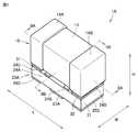
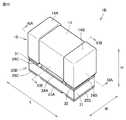
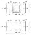
図1は、本発明の実施の形態1に係る集合基板120A(図6および図7参照)を用いて製作された抵抗素子20Aを備える複合電子部品1Aの概略的な斜視図である。図2(A)および図2(B)は、それぞれ図1中に示されるIIA−IIA線およびIIB−IIB線に沿って複合電子部品1Aが切断された場合の模式的な断面図である。図3(A)から図3(C)は、それぞれ図1に示される抵抗素子20Aの模式的な上面図、断面図および下面図である。また、図4は、図1に示される複合電子部品1Aが分解された模式的な斜視図である。
FIG. 1 is a schematic perspective view of a composite
まず、本実施の形態に係る集合基板120Aを説明するに先立って、図1から図4を参照して、当該集合基板120Aを用いて製作された抵抗素子20Aならびにこの抵抗素子20Aを備える複合電子部品1Aについて説明する。なお、以下において説明する複合電子部品1Aは、本実施の形態に係る集合基板120Aを用いて製作された抵抗素子20Aを利用する場合の一つの態様を例示的に示したものに過ぎず、他の態様にて当該抵抗素子20Aを利用することも当然に可能である。 First, prior to describing the
図1、図2および図4に示されるように、複合電子部品1Aは、2つの電子素子を備えている。すなわち、複合電子部品1Aは、第1の電子素子としてコンデンサ素子10と、第2の電子素子として抵抗素子20Aとを備えている。 As shown in FIGS. 1, 2 and 4, the composite
主に図1および図4に示されるように、コンデンサ素子10は、略直方体形状を有し、長さ方向Lに沿った4辺の寸法が、幅方向Wに沿った4辺の寸法よりも大きい。ここで言う略直方体形状には、直方体の角部および稜部の一部または全てに丸み等が設けられたものや、直方体の表面、すなわち6面の一部または全てに段差や凹凸等が設けられたもの等が含まれる。 As mainly shown in FIGS. 1 and 4,
同じく主に図1および図4に示されるように、抵抗素子20Aは、所定の厚みを有する略平板形状を有し、長さ方向Lに沿った4辺の寸法が、幅方向Wに沿った4辺の寸法よりも大きい。ここで言う略平板形状には、抵抗素子20Aの角部および稜部の一部または全てに丸み等が設けられたものや、抵抗素子20Aの表面、すなわち6面の一部または全てに段差や凹凸等が設けられたもの等が含まれる。 Similarly, as mainly shown in FIG. 1 and FIG. 4, the
図1、図2および図4に示されるように、コンデンサ素子10は、抵抗素子20A上に配置されている。この配置では、コンデンサ素子10の下面11aと、抵抗素子20Aの上面21aとが対向している。そして図1および図2に示されるように、コンデンサ素子10が、第1接合材31および第2接合材32を介して抵抗素子20Aに接合されている。 As shown in FIG. 1, FIG. 2 and FIG. 4, the
以下の説明では、複合電子部品1Aの構成を具体的に説明するために、コンデンサ素子10と抵抗素子20Aとが並ぶ方向を高さ方向Hと呼ぶ。そして、この高さ方向Hに直交する方向のうち、コンデンサ素子10の第1外部電極14Aおよび第2外部電極14Bが並ぶ方向を長さ方向Lと呼ぶ。また、この高さ方向Hおよび長さ方向Lのいずれにも直交する方向を幅方向Wと呼ぶ。第1外部電極14Aおよび第2外部電極14Bについては、後に詳述する。 In the following description, in order to specifically describe the configuration of the composite
図1、図2および図4に示されるように、コンデンサ素子10は、たとえば積層セラミックコンデンサであり、コンデンサ本体11と、このコンデンサ本体11の表面に設けられた第1外部電極14Aおよび第2外部電極14Bとを有している。コンデンサ本体11は、略直方体形状を有しており、その表面の所定の領域に設けられた第1外部電極14Aおよび第2外部電極14Bは、長さ方向Lにおいて互いに離隔している。 As shown in FIG. 1, FIG. 2 and FIG. 4,
図2に示されるように、コンデンサ本体11は、複数の誘電体層12および複数の内部電極層13からなり、複数の誘電体層12のうちの各一層と複数の内部電極層13のうちの各一層とが交互に積層されて構成されている。図示する複合電子部品1Aでは、複数の誘電体層12および複数の内部電極層13の積層方向が、高さ方向Hと概ね一致している。ただし、これは一例にすぎず、複数の誘電体層12および複数の内部電極層13の積層方向は、幅方向Wに概ね一致していてもよい。 As shown in FIG. 2, the capacitor
複数の誘電体層12は、たとえばチタン酸バリウム(BaTiO3)、チタン酸カルシウム(CaTiO3)、チタン酸ストロンチウム(SrTiO3)、またはジルコン酸カルシウム(CaZrO3)等を主成分とするセラミック材料を含む材料からなる。また、複数の誘電体層12は、主成分よりも含有量の少ない副成分として、Mn、Mg、Si、Co、Ni、または希土類等を含んでいてもよい。一方、複数の内部電極層13は、たとえばNi、Cu、Ag、Pd、Ag−Pd合金、またはAu等の金属材料を含む材料からなる。The plurality of
第1外部電極14Aおよび第2外部電極14Bは、いずれも下地導電層および被覆導電層を含む複数の導電層にて構成されている。下地導電層は、コンデンサ本体11の表面の一部に直接設けられた導電層を意味し、被覆導電層は、下地電極層を覆う導電層を意味する。下地導電層は、たとえば焼結金属層であり、焼結金属層とは、Cu、Ni、Ag、Pd、Ag−Pd合金、またはAu等とガラスを含むペーストを焼き付けることで形成された層を意味する。被覆導電層は、たとえばめっき層であり、めっき層とは、めっき処理で形成された層である。被覆導電層は、たとえばNiを含むめっき層およびSnを含むめっき層である。また、被覆導電層は、Cuを含むめっき層やAuを含むめっき層であってもよい。 Each of the first
なお、第1外部電極14Aおよび第2外部電極14Bは、下地導電層を省略してめっき層のみによって構成されていてもよい。また、下地導電層は、金属成分と樹脂成分とを含む導電性樹脂ペーストを硬化させた導電性の樹脂層で構成されていてもよい。 The first
図1および図2に示されるように、コンデンサ本体11は、長さ方向Lにおいて相対する一対の端面と、幅方向Wにおいて相対する一対の側面と、高さ方向Hにおいて相対する一対の主面とを有している。このうち、高さ方向Hにおいて相対する一対の主面のうちの一方である下面11aが、抵抗素子20Aに対向している。 As shown in FIGS. 1 and 2, the
また、第1外部電極14Aは、コンデンサ本体11の一方の端面と、上記一対の側面および上記一対の主面のそれぞれの一部とに連なって設けられており、第2外部電極14Bは、コンデンサ本体11の他方の端面と、上記一対の側面および上記一対の主面のそれぞれの一部とに連なって設けられている。これにより、コンデンサ本体11の下面11aは、第1外部電極14Aが設けられた領域と、第2外部電極14Bが設けられた領域と、それらが設けられておらずコンデンサ本体11の一部が露出した領域とに分けることができる。 In addition, the first
図2に示されるように、高さ方向Hに沿って複数の誘電体層12のうちの1層を挟んで隣り合う、複数の内部電極層13の2層のうちの一方は、コンデンサ本体11の一方の端面に引き出されて第1外部電極14Aに接続された第1内部電極層である。そして、他方は、コンデンサ本体11の他方の端面に引き出されて第2外部電極14Bに接続された第2内部電極層である。これにより、第1外部電極14Aおよび第2外部電極14Bは、複数のコンデンサが電気的に並列に接続された状態を構成する。 As shown in FIG. 2, one of two layers of the plurality of internal electrode layers 13 adjacent to each other across one of the plurality of
上述したコンデンサ素子10は、たとえば、以下の手順で製造される。まず、誘電体層12となるセラミックグリーンシートの表面に内部電極層13となる導電性ペーストが印刷されてなる複数の素材シートを交互に積層して圧着することにより、積層チップが得られる。ここで、複数の積層チップが一体化された積層ブロックが始めに製作され、その後この積層ブロックが切り離されて、積層チップが製作されてもよい。次に、この積層チップが焼成されて、コンデンサ本体11が得られる。そしてその後、コンデンサ本体11の表面に第1外部電極14Aおよび第2外部電極14Bが形成されて、上述したコンデンサ素子10が製造される。
なお、コンデンサ素子10の大きさは、特に制限されるものではないが、一例としては、その長さ方向Lの寸法が0.60[mm]であり、その幅方向Wの寸法が0.30[mm]であり、その高さ方向Hの寸法が0.30[mm]である。 Although the size of the
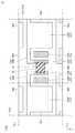
図1から図4に示されるように、抵抗素子20Aは、絶縁性の基部21と、抵抗体22と、保護膜23と、第1上面導体24A、第2上面導体24B、第3上面導体24Cおよび第4上面導体24D(以下、総じて「第1上面導体24Aから第4上面導体24D」と記載する場合もある。)と、第1下面導体25A、第2下面導体25B、第3下面導体25Cおよび第4下面導体25D(以下、総じて「第1下面導体25Aから第4下面導体25D」と記載する場合もある。)と、第1接続導体26A、第2接続導体26B、第3接続導体26Cおよび第4接続導体26D(以下、総じて「第1接続導体26Aから第4接続導体26D」と記載する場合もある。)とを有している。 As shown in FIGS. 1 to 4, the
主に図2に示されるように、基部21は、所定の厚みを有する略平板形状を有しており、たとえばエポキシ樹脂等の樹脂材料やアルミナ等のセラミック材料、あるいはこれらに無機材料または有機材料からなるフィラーや織布等が添加されたもの等にて構成される。より好ましくは、アルミナ基板や、低温同時焼成セラミック(LTCC)基板を含むセラミック基板が、基部21として利用される。図示する抵抗素子20Aにあっては、基部21が2層のセラミックグリーンシートが積層されて一体化されてなるLTCC基板にて構成されている。 As mainly shown in FIG. 2, the
基部21は、長さ方向Lにおいて相対する一対の側面である第1側面および第2側面と、幅方向Wにおいて相対する一対の側面である第3側面および第4側面と、高さ方向Hにおいて相対する一対の主面とを有している。図2および図4に示されるように、一対の主面のうちの一方である上面21aが、コンデンサ素子10の下面11aと向かい合い、一対の主面のうちの他方である下面21bが、複合電子部品1Aが実装される、図示が省略された配線基板と対向する。 The
図2および図3に示されるように、抵抗体22は、基部21の上面21aの所定位置に設けられている。高さ方向Hに沿って抵抗素子20Aが平面視された場合に、抵抗体22はたとえば矩形または円形の膜形状を有している。抵抗体22としては、用途に応じて種々の材料を用いることができるが、たとえば金属皮膜、酸化金属皮膜、または酸化金属皮膜とガラスとの混合物であるメタルグレーズ被膜等が利用できる。温度特性等の観点からは、抵抗体22は、金属材料にて構成されていることが好ましい。 As shown in FIGS. 2 and 3, the
なお、抵抗体22は、ペーストが塗布され、塗布されたペーストが焼き付けられる、いわゆる厚膜形成プロセスによって形成される厚膜で構成されていてもよいし、スパッタリング法や金属蒸着法等のいわゆる薄膜形成プロセスによって形成される薄膜で構成されていてもよい。抵抗体22を厚膜で構成する場合には、その厚みは、たとえば5[μm]以上30[μm]以下であり、抵抗体22を薄膜で構成する場合には、その厚みは、たとえば10[nm]以上30[nm]以下である。 The
図2および図3に示されるように、保護膜23は、基部21の上面21a上において抵抗体22を覆っており、たとえばガラスまたはSiO2等の無機材料や、エポキシ樹脂またはポリイミド樹脂等の樹脂材料、あるいはこれらの複合膜等からなる絶縁性の膜で構成されている。保護膜23の厚みは、たとえば5[μm]以上30[μm]以下である。ここで、保護膜23は、抵抗体22が露出されることがないように、抵抗体22を完全に覆っていることが好ましい。As shown in FIGS. 2 and 3, the
図2から図4、特に図3(A)に示されるように、第1上面導体24Aから第4上面導体24Dは、いずれも基部21の上面21aに設けられている。第1上面導体24Aから第4上面導体24Dの各々は、高さ方向Hに沿って抵抗素子20Aが平面視されたときに、長さ方向Lの寸法が幅方向Wの寸法よりも小さい矩形状に構成されている。 As shown in FIG. 2 to FIG. 4, particularly FIG. 3 (A), the first
第1上面導体24Aと第2上面導体24Bとは、基部21の中心を挟んで長さ方向Lにおいて離隔しており、第1上面導体24Aは、長さ方向Lにおいて基部21の中心と第1側面との間に配置され、第2上面導体24Bは、長さ方向Lにおいて基部21の中心と第2側面との間に配置されている。第3上面導体24Cは、基部21の長さ方向Lに沿った第1側面側の端部に配置され、第4上面導体24Dは、基部21の長さ方向Lに沿った第2側面側の端部に配置されている。すなわち、第1上面導体24Aおよび第2上面導体24Bは、長さ方向Lにおいて第3上面導体24Cと第4上面導体24Dとの間に位置している。 The first
また、第1上面導体24Aから第4上面導体24Dの各々の幅方向Wにおける両端は、基部21の幅方向Wに沿った両端にそれぞれ達している。すなわち、第1上面導体24Aから第4上面導体24Dの幅方向Wにおける寸法は、いずれも同じである。 Further, both ends in the width direction W of each of the first
第1上面導体24Aおよび第2上面導体24Bのそれぞれの長さ方向Lの寸法は、たとえば0.06[mm]であり、第3上面導体24Cおよび第4上面導体24Dのそれぞれの長さ方向Lの寸法は、たとえば0.1[mm]である。また、第1上面導体24Aと第3上面導体24Cとの間の長さ方向Lの距離および第2上面導体24Bと第4上面導体24Dとの間の長さ方向Lの距離は、それぞれたとえば0.07[mm]であり、第1上面導体24Aと第2上面導体24Bとの間の長さ方向Lの距離は、たとえば0.14[mm]である。 The dimension in the length direction L of each of the first
第3上面導体24Cおよび第4上面導体24Dの長さ方向Lの寸法は、第1上面導体24Aおよび第2上面導体24Bの長さ方向Lの寸法よりも大きいことが好ましい。この場合には、コンデンサ素子10と抵抗素子20Aとの接合強度を高めるとともに、抵抗体22の面積が広くなるので、抵抗体22の電気特性を調整するための自由度を高めることができる。 The dimension in the length direction L of the third
第1上面導体24Aと第3上面導体24Cとの間の長さ方向Lの距離および第2上面導体24Bと第4上面導体24Dとの間の長さ方向Lの距離は、第1上面導体24Aと第2上面導体24Bとの間の長さ方向Lの距離よりも小さいことが好ましい。この場合には、コンデンサ素子10と抵抗素子20Aとの接合強度を高めるとともに、抵抗体22の面積が広くなるので、抵抗体22の電気特性を調整するための自由度を高めることができる。 The distance in the longitudinal direction L between the first
図2から図4、特に図3(C)に示されるように、第1下面導体25Aから第4下面導体25Dは、いずれも基部21の下面21bに設けられている。第1下面導体25Aおよび第2下面導体25Bの各々は、高さ方向Hに沿って抵抗素子20Aが平面視されたときに、長さ方向Lの寸法が幅方向Wの寸法よりも大きい矩形状に構成されている。第3下面導体25Cおよび第4下面導体25Dの各々は、高さ方向Hに沿って抵抗素子20Aが平面視されたときに、長さ方向Lの寸法が幅方向Wの寸法よりも小さい矩形状に構成されている。 As shown in FIG. 2 to FIG. 4, particularly FIG. 3 (C), the first
第1下面導体25Aと第2下面導体25Bとは、基部21の中心を挟んで幅方向Wにおいて離隔しており、第1下面導体25Aは、基部21の幅方向Wに沿った第3側面側の端部に配置され、第2下面導体25Bは、基部21の幅方向Wに沿った第4側面側の端部に配置されている。第3下面導体25Cは、基部21の長さ方向Lに沿った第1側面側の端部に配置され、第4下面導体25Dは、基部21の長さ方向Lに沿った第2側面側の端部に配置されている。すなわち、第1下面導体25Aおよび第2下面導体25Bは、長さ方向Lにおいて第3下面導体25Cと第4下面導体25Dとの間に位置している。なお、第3下面導体25Cは、基部21を挟んで第3上面導体24Cと相対しており、第4下面導体25Dは、基部21を挟んで第4上面導体24Dと相対している。 The first
図2および図3、特に図3(B)に示されるように、基部21の内部には、第1接続導体26Aから第4接続導体26Dが設けられている。 As shown in FIGS. 2 and 3, particularly in FIG. 3 (B), the
第1接続導体26Aは、埋め込み配線層として内部接続導体26A1と、基部21を高さ方向Hに貫通する一対の上側ビア導体26A2および下側ビア導体26A3とを含んでいる。上側ビア導体26A2および下側ビア導体26A3は、高さ方向Hに沿って平面視された場合に、略円形状を有している。第1接続導体26Aは、第1上面導体24Aと第1下面導体25Aとを接続している。 The
第2接続導体26Bは、埋め込み配線層として内部接続導体26B1と、基部21を高さ方向Hに貫通する一対の上側ビア導体26B2および下側ビア導体26B3とを含んでいる。上側ビア導体26B2および下側ビア導体26B3は、高さ方向Hに沿って平面視された場合に、略円形状を有している。第2接続導体26Bは、第2上面導体24Bと第2下面導体25Bとを接続している。 The
第3接続導体26Cは、基部21を高さ方向Hに沿って貫通するビア導体であり、高さ方向Hに沿って平面視された場合に、略円形状を有している。第3接続導体26Cは、高さ方向Hに沿って平面視された場合に、第3上面導体24Cおよび第3下面導体25Cに重なっており、第3上面導体24Cと第3下面導体25Cとを接続している。 The
第4接続導体26Dは、基部21を高さ方向Hに沿って貫通するビア導体であり、高さ方向Hに沿って平面視された場合に、略円形状を有している。第4接続導体26Dは、高さ方向Hに沿って平面視された場合に、第4上面導体24Dおよび第4下面導体25Dに重なっており、第4上面導体24Dと第4下面導体25Dとを接続している。 The
ここで、第1上面導体24Aと第2上面導体24Bとを長さ方向Lにおいて互いにより離れるように構成した場合には、高さ方向Hから平面視されたときに、第1上面導体24Aと第1下面導体25Aとが重なる領域が小さく、また、第2上面導体24Bと第2下面導体25Bとが重なる領域が小さい。 Here, when the first
このような場合であっても、第1接続導体26Aを、基部21の内部において高さ方向Hと直交する方向に延びる内部接続導体26A1と、基部21の内部において高さ方向Hに延びる上側ビア導体26A2および下側ビア導体26A3とによって構成することにより、第1上面導体24Aと第1下面導体25Aを接続することができる。また、第2接続導体26Bを、基部21の内部において高さ方向Hと直交する方向に延びる内部接続導体26B1と、基部21の内部において高さ方向Hに延びる上側ビア導体26B2および下側ビア導体26B3とによって構成することにより、第2上面導体24Bと第2下面導体25Bを接続することができる。 Even in such a case, the inner connecting conductor 26A1 extending in the direction perpendicular to the height direction H inside the
より詳細には、高さ方向Hに沿って平面視されたときに、内部接続導体26A1は、基部21の内部において長さ方向Lおよび幅方向Wに延びるL字形状を有している。上側ビア導体26A2は、内部接続導体26A1に接続され、内部接続導体26A1から基部21の上面21aに向かって高さ方向Hに延びる。下側ビア導体26A3は、内部接続導体26A1に接続され、内部接続導体26A1から基部21の下面21bに向かって高さ方向Hに延びる。ここで、高さ方向Hから平面視されて、上側ビア導体26A2と下側ビア導体26A3とは、少なくとも一部において重なっていない。 More specifically, when viewed in plan along the height direction H, the internal connection conductor 26A1 has an L shape extending in the length direction L and the width direction W inside the
このように構成することにより、平面視して第1上面導体24Aと第1下面導体25Aとが重なる領域が小さい場合にも、これら第1上面導体24Aと第1下面導体25Aとを、内部接続導体26A1、上側ビア導体26A2および下側ビア導体26A3を介して接続することが可能になる。 With this configuration, even when the area where the first
また、高さ方向Hに沿って平面視されたときに、内部接続導体26B1は、基部21の内部において長さ方向Lおよび幅方向Wに延びるL字形状を有している。上側ビア導体26B2は、内部接続導体26B1に接続され、内部接続導体26B1から基部21の上面21aに向かって高さ方向Hに延びる。下側ビア導体26B3は、内部接続導体26B1に接続され、内部接続導体26B1から基部21の下面21bに向かって高さ方向Hに延びる。ここで、高さ方向Hから平面視されて、上側ビア導体26B2と下側ビア導体26B3とは、少なくとも一部において重なっていない。 Further, when viewed in plan along the height direction H, the internal connection conductor 26B1 has an L shape extending in the length direction L and the width direction W inside the
このように構成することにより、平面視して第2上面導体24Bと第2下面導体25Bとが重なる領域が小さい場合にも、これら第2上面導体24Bと第2下面導体25Bとを、内部接続導体26B1、上側ビア導体26B2および下側ビア導体26B3を介して接続することが可能になる。 By this configuration, even when the area where the second
したがって、上記構成を採用することにより、高さ方向Hから平面視された場合の第1上面導体24Aおよび第2上面導体24Bの配置と第1下面導体25Aおよび第2下面導体25Bの配置とを容易に異ならせることが可能になる。ただし、設計が許す限りにおいては、実装安定性の観点およびショート不良の発生の防止の観点から、基部の上面または下面に到達しかつ抵抗素子の外表面に露出することになるビア導体は、上面導体および下面導体と完全に重ならせることが好ましい。 Therefore, by adopting the above configuration, the arrangement of the first
なお、高さ方向Hから平面視された場合に上側ビア導体と下側ビア導体とが重なるように配置できる場合には、内部接続導体を形成せずに上側ビア導体と下側ビア導体とを直接接続することとしてもよい。 When the upper via conductor and the lower via conductor can be arranged so as to overlap with each other in plan view from the height direction H, the upper via conductor and the lower via conductor can be formed without forming the internal connection conductor. It is also possible to connect directly.
ここで、第1上面導体24Aおよび第2上面導体24Bは、保護膜23によって覆われていない部分と保護膜23によって覆われている部分とに分けられる。また、第3上面導体24Cおよび第4上面導体24Dは、そのすべてが保護膜23によって覆われていない部分となる。 Here, the first
各上面導体の保護膜23によって覆われていない部分は、たとえば下地導電層および2層の被覆導電層を含む複数の導電層にて構成されている。下地導電層は、たとえば焼結金属層であり、具体的にはCuとガラスを含むペーストを焼き付けることで形成されたCuを含む焼結金属層であることが好ましい。また、下地導電層は、スパッタリング法や金属蒸着法等のいわゆる薄膜形成プロセスによって形成される薄膜であってもよい。2層の被覆導電層は、それぞれたとえばめっき処理で形成されたNiを含むめっき層およびこれを覆うAuを含むめっき層であることが好ましい。 The portion not covered by the
一方、各上面導体の保護膜23によって覆われている部分は、たとえば2層の被覆導電層を含んでおらず、下地導電層のみにて構成されている。これは、後述するように、下地導電層が形成された後であって被覆導電層が形成される前に、各上面導体の一部が保護膜23によって覆われることによって実現される。 On the other hand, the portion covered by the
なお、第1下面導体25Aから第4下面導体25Dは、いずれもたとえば下地導電層および2層の被覆導電層を含む複数の導電層にて構成されている。 Each of the first to fourth
Cuを含む焼結金属層は、Cuとガラスを含むペーストを焼き付ける、いわゆる厚膜形成プロセスによって形成される厚膜であり、その厚みは、たとえば10[μm]以上30[μm]以下程度とされる。なお、下地導電層には、Cuを含む焼結金属層の他にも、Agを含む焼結金属層等が利用できる。また、下地導電層を薄膜で構成する場合には、これをCuまたはAgを含む薄膜にて構成することが好ましく、その厚みは、たとえば10[nm]以上30[nm]以下程度とされる。 The sintered metal layer containing Cu is a thick film formed by a so-called thick film forming process by baking a paste containing Cu and glass, and its thickness is, for example, about 10 μm to 30 μm or less. Ru. In addition to the sintered metal layer containing Cu, a sintered metal layer containing Ag or the like can be used as the base conductive layer. When the underlying conductive layer is formed of a thin film, it is preferably formed of a thin film containing Cu or Ag, and the thickness thereof is, for example, about 10 nm to 30 nm.
一方、Niを含むめっき層およびAuを含むめっき層の総厚みは、たとえば3[μm]以上30[μm]以下とされる。なお、被覆導電層の材質としては、接合材に応じて適宜選択することができ、たとえばCu、Ag、Au、NiまたはSn等から選択される。 On the other hand, the total thickness of the plating layer containing Ni and the plating layer containing Au is, for example, 3 μm or more and 30 μm or less. The material of the covering conductive layer can be appropriately selected according to the bonding material, and is selected, for example, from Cu, Ag, Au, Ni, or Sn.
上述した抵抗体22は、長さ方向Lにおいて第1上面導体24Aが設けられた領域と第2上面導体24Bが設けられた領域との間に主として位置しており、高さ方向Hから平面視された場合に、抵抗体22の長さ方向Lにおける一端が第1上面導体24Aの一部と重なっているとともに、抵抗体22の長さ方向Lにおける他端が第2上面導体24Bの一部と重なっている。これにより、第1上面導体24Aおよび第2上面導体24Bが、抵抗体22に接続される。 The
なお、本実施の形態に係る抵抗素子20Aの大きさは、特に制限されるものではないが、一例としては、その長さ方向Lの寸法が0.60[mm]であり、その幅方向Wの寸法が0.30[mm]であり、その高さ方向Hの寸法が0.14[mm]である。 The size of the
また、抵抗素子20Aは、第2上面導体24Bを含まず、基部21の上面に第1上面導体24Aと第3上面導体24Cと第4上面導体24Dの3つの上面導体のみを有してもよい。この場合には、抵抗体22は、第2上面導体24Bに代えて、第3上面導体24Cまたは第4上面導体24Dに接続される。また、この場合には、抵抗素子20Aは、第2下面導体25Bおよび第2接続導体26Bを含まなくてもよい。 The
以上において説明した複合電子部品1Aに備えられる基板型の電子素子としての抵抗素子20Aは、複数の抵抗素子20Aが一体化された集合基板120A(図6および図7参照)を製作し、これを個片化することによって製造される。以下、その製造工程について説明した後に、本実施の形態に係る抵抗素子用集合基板120Aについて詳説する。
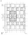
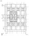
図5は、図1に示される抵抗素子20Aの製造フローを示す図である。また、図6は、本実施の形態に係る集合基板120Aの模式的な上面図であり、図7は、図6中に示す単位領域VIIを拡大した模式的な上面図である。 FIG. 5 is a diagram showing a manufacturing flow of the
図5に示されるように、まず、セラミックグリーンシートが製作される(工程ST1)。具体的には、セラミック粉末、バインダ樹脂および溶媒等が所定の配合比率で混合されることでセラミックスラリーが調製される。このセラミックスラリーがキャリアフィルム上において、ダイコーティング、グラビアコーティング、マイクログラビアコーティング、スクリーン印刷、またはスプレーコーティング等によってシート状に塗布されることにより、セラミックグリーンシートが形成される。形成されたセラミックグリーンシートは、抵抗素子20Aの集合体であるマザー基板121(図6および図7参照)となるものであり、また、抵抗素子20Aの基部21となるものである。 As shown in FIG. 5, first, a ceramic green sheet is manufactured (step ST1). Specifically, the ceramic slurry is prepared by mixing the ceramic powder, the binder resin, the solvent and the like at a predetermined blending ratio. The ceramic slurry is applied in a sheet form on a carrier film by die coating, gravure coating, microgravure coating, screen printing, spray coating or the like to form a ceramic green sheet. The formed ceramic green sheet is to be a mother substrate 121 (see FIGS. 6 and 7) which is an assembly of the
次に、孔あけ加工が施される(工程ST2)。具体的には、セラミックグリーンシートが2枚用意され、そのそれぞれの所定位置に複数の貫通孔が形成される。ここで、当該貫通孔の形成は、上側ビア導体26A2および26B2ならびに下側ビア導体26A3および26B3を形成するための前処理となる。 Next, a drilling process is performed (step ST2). Specifically, two ceramic green sheets are prepared, and a plurality of through holes are formed in their respective predetermined positions. Here, the formation of the through holes is a pretreatment for forming the upper via conductors 26A2 and 26B2 and the lower via conductors 26A3 and 26B3.
次に、導電性ペーストが印刷される(工程ST3)。具体的には、2枚のセラミックグリーンシートの一方の上面と他方の下面に、導電性ペーストとしてCuペーストがスクリーン印刷法またはグラビア印刷法等によって印刷される。これにより、2枚のセラミックグリーンシートの一方の上面に第1上面導体24Aおよび第2上面導体24Bの下地導電層となる部分を含むCuペーストからなる所定形状の導電パターンが形成され、さらに、他方のセラミックグリーンシートの下面に第1下面導体25Aから第4下面導体25Dの下地導電層となる部分を含むCuペーストからなる所定形状の導電パターンが形成される。 Next, a conductive paste is printed (step ST3). Specifically, Cu paste is printed as a conductive paste on the upper surface and lower surface of one of the two ceramic green sheets by a screen printing method, a gravure printing method, or the like. As a result, a conductive pattern of a predetermined shape formed of Cu paste is formed on the upper surface of one of the two ceramic green sheets, including a portion to be the base conductive layer of the first
なお、その際、2枚のセラミックグリーンシートに設けられた複数の貫通孔が上側ビア導体26A2および26B2ならびに下側ビア導体26A3および26B3となるCuペーストにて埋め込まれるとともに、2枚のセラミックグリーンシートの一方の下面または他方の上面に内部接続導体26A1および26B1となるCuペーストからなる所定形状の導電パターンも印刷される。 At this time, the plurality of through holes provided in the two ceramic green sheets are embedded with Cu paste to be the upper via conductors 26A2 and 26B2 and the lower via conductors 26A3 and 26B3, and the two ceramic green sheets A conductive pattern of a predetermined shape made of Cu paste, which becomes the internal connection conductors 26A1 and 26B1, is also printed on one lower surface or the upper surface of the other.
次に、貼り合わせおよび焼成が行なわれる(工程ST4)。具体的には、上述した2枚のセラミックグリーンシートが貼り合わされ、貼り合わされた2枚のセラミックグリーンシートが所定の温度に加熱されることにより、2枚のセラミックグリーンシートおよびこれら2枚のセラミックグリーンシート上に印刷されたCuペーストからなる導電パターンの焼結処理が行なわれる。その結果、2枚のセラミックグリーンシートが一体化して硬質のマザー基板121に変化し、導電パターンが焼結金属層に変化する。これにより、マザー基板121には、第1上面導体24Aから第4上面導体24Dおよび第1下面導体25Aから第4下面導体25Dの一部となる下地導電層ならびに第1接続導体26Aから第4接続導体26Dが形成される。 Next, bonding and firing are performed (step ST4). Specifically, the two ceramic green sheets described above are bonded together, and the two bonded ceramic green sheets are heated to a predetermined temperature to obtain two ceramic green sheets and these two ceramic green sheets. A sintering process is performed on the conductive pattern made of Cu paste printed on the sheet. As a result, the two ceramic green sheets are integrated and changed to a
次に、抵抗体ペーストが印刷される(工程ST5)。具体的には、マザー基板121の上面121a(図6および図7参照)に、抵抗体ペーストが、スクリーン印刷法またはグラビア印刷法等を用いて印刷される。これにより、マザー基板121の上面121aに抵抗体ペーストからなる抵抗体パターンが形成されることになる。なおその際、第1上面導体24Aおよび第2上面導体24Bとなる下地導電層の一部にこれら抵抗体パターンが重なるように印刷が行なわれる。 Next, a resistor paste is printed (step ST5). Specifically, the resistor paste is printed on the
次に、抵抗体ペーストが焼き付けられる(工程ST6)。具体的には、ここまでの仕掛品が所定の温度に加熱されて、マザー基板121上に印刷された抵抗体ペーストの焼結処理が行なわれる。その結果、抵抗体パターンがマザー基板121に焼き付けられて、マザー基板121には、抵抗体22が形成される。 Next, the resistor paste is baked (step ST6). Specifically, the work-in-process to this point is heated to a predetermined temperature, and the sintering process of the resistor paste printed on the
次に、抵抗体のトリミングが行なわれる(工程ST7)。具体的には、抵抗体22にレーザー光が照射されてその一部が除去されることにより、抵抗体22に平面視L字状の除去痕(図3(A)中において示される符号22aで示される部分)が形成され、これにより抵抗体22の抵抗値の調整が行なわれる。なお、当該トリミングに際しては、後述する、マザー基板121上に別途設けられた電極部125Aおよび125B(図7参照)に抵抗計のプローブが押し当てられ、この状態において抵抗体22の抵抗値がモニタされつつレーザー光の照射が行なわれる。これにより、抵抗体22の抵抗値の微調整が実現できることになる。 Next, trimming of the resistor is performed (step ST7). Specifically, laser light is irradiated to the
次に、保護膜が塗布され(工程ST8)、次いで塗布された保護膜の硬化処理が行なわれる(工程ST9)。具体的には、抵抗体22と、この抵抗体22に接続された第1上面導体24Aおよび第2上面導体24Bとなる下地導電層の一部とを覆うように保護膜23が塗布される。その後、ここまでの仕掛品が所定の温度に加熱されて、当該保護膜23がマザー基板121に付着した状態で硬化する。 Next, a protective film is applied (step ST8), and then the applied protective film is cured (step ST9). Specifically, the
次に、マザー基板が切断される(工程ST10)。具体的には、いわゆる押し切りやダイシング等の方法によってマザー基板121が所定の切断ラインCL1およびCL2(図6および図7参照)に沿って切断されることにより、個々の抵抗素子20Aが切り出される。 Next, the mother substrate is cut (step ST10). Specifically, individual
次に、めっき処理が施される(工程ST11)。具体的には、ここまでの仕掛品がNiめっき浴およびAuめっき浴に順次浸漬されることにより、抵抗素子20Aに設けられた下地導電層に対するめっき処理が実施され、被覆導電層が形成される。これにより、これら下地導電層がNiを含むめっき層によって覆われ、Niを含むめっき層がAuを含むめっき層によって覆われる。その結果、第1上面導体24Aから第4上面導体24Dおよび第1下面導体25Aから第4下面導体25Dが、それぞれ形成される。以上により、抵抗素子20Aの製造が完了する。 Next, a plating process is performed (step ST11). Specifically, by plating the work-in-process to this point sequentially in the Ni plating bath and the Au plating bath, the plating process is performed on the base conductive layer provided on
なお、図4を参照して、抵抗素子20Aにコンデンサ素子10が実装されるに際しては、まず抵抗素子20Aに接合材が印刷され、次いでコンデンサ素子10が抵抗素子20Aに載置され、その後リフローが行なわれる。具体的には、第3上面導体24Cおよび第4上面導体24Dを覆うように、半田ペーストからなる第1接合材31および第2接合材32がそれぞれスクリーン印刷法等によって印刷され、第1接合材31上に第1外部電極14Aが配置されかつ第2接合材32上に第2外部電極14Bが配置されるように、コンデンサ素子10が抵抗素子20Aに載置される。その後、当該仕掛品がリフロー炉等に投入されることによって半田付けが行なわれ、第3上面導体24Cと第1外部電極14Aとが第1接合材31によって接合され、第4上面導体24Dと第2外部電極14Bとが第2接合材32によって接合される。これにより、コンデンサ素子10が抵抗素子20Aに対して実装されることになり、複合電子部品1Aが製造されることになる。 Referring to FIG. 4, when
ここで、図6に示されるように、本実施の形態に係る集合基板120Aにあっては、切断後に基部21となるマザー基板121が、行列状に互いに離隔して配置された、切断後において抵抗素子20Aとなる複数の製品予定領域Raと、これら複数の製品予定領域Raの間に位置する格子状の切除予定領域(当該切除予定領域には、後述する第1領域Rb1、第2領域Rb2および第3領域Rb3が含まれる)とを有している。このように構成しつつ、マザー基板121の上面121a上における導電パターンのレイアウトを工夫することにより、切除予定領域の大型化を抑制しつつ、抵抗素子20Aの取り個数を多く確保することが実現できる。 Here, as shown in FIG. 6, in the
以下、その詳細について説明する。ここで、図6においては、上述した保護膜の硬化処理(すなわち工程ST9)後のマザー基板121の状態が表わされており、図7においては、本実施の形態に係る集合基板120Aの構成の理解を容易とするために、上述した抵抗体ペーストの焼き付け(すなわち工程ST6)後のマザー基板121の状態が表わされている。なお、図6および図7中に示すX軸方向およびY軸方向は、複数の製品予定領域Raが並ぶ方向である行方向および列方向の一方および他方を表わしており、それぞれ上述した抵抗素子20Aにおける長さ方向Lおよび幅方向Wに合致している。 The details will be described below. Here, FIG. 6 shows the state of the
図6に示されるように、マザー基板121の上面121aには、X軸方向における端部を除き、平面視された場合に略E字状である複数の導電パターン(第1導電パターンP1および第2導電パターンP2)と、平面視された場合に略矩形状である複数の導電パターン(第3導電パターンP3および第4導電パターンP4)と、複数の抵抗体22と、複数の保護膜23とが設けられている。 As shown in FIG. 6, on the
略E字状の複数の導電パターンP1、P2は、X軸方向およびY軸方向に沿って行列状に配置されている。略矩形状の複数の導電パターンP3、P4は、略E字状の導電パターンP1、P2の各々の内側に当該略E字状の導電パターンP1、P2と離隔されることで電気的に絶縁されて一対設けられている。より詳細には、略矩形状の複数の導電パターンP3、P4の各々の三辺は、略E字状の複数の導電パターンP1、P2の辺の一部とそれぞれ向き合っており、残る一辺は、略E字状の複数の導電パターンP1、P2の辺とそれぞれ向き合っていない。 The plurality of substantially E-shaped conductive patterns P1 and P2 are arranged in a matrix along the X-axis direction and the Y-axis direction. The plurality of substantially rectangular conductive patterns P3 and P4 are electrically insulated by being separated from the substantially E-shaped conductive patterns P1 and P2 inside each of the substantially E-shaped conductive patterns P1 and P2. A pair is provided. More specifically, the three sides of each of the plurality of substantially rectangular conductive patterns P3 and P4 respectively face part of the sides of the plurality of substantially E-shaped conductive patterns P1 and P2, and the remaining side is The sides of the plurality of substantially E-shaped conductive patterns P1 and P2 do not face each other.
複数の抵抗体22は、それぞれX軸方向において隣り合う一対の略E字状の導電パターンP1、P2に重なるように配置されている。複数の保護膜23は、複数の抵抗体22のそれぞれを覆うように配置されている。複数の保護膜23の各々は、抵抗体22に接続された部分の略E字状の複数の導電パターンP1、P2をさらに覆っている。 The plurality of
上述したように、複数の製品予定領域Raは、行列状に互いに離隔して配置されている。ここで、複数の製品予定領域Raのうちの任意の1つの製品予定領域と、切除予定領域のうちの上記任意の1つの製品予定領域を取り囲む部分である枠状領域とからなる部分を単位領域VIIとした場合、枠状領域は、X軸方向において製品予定領域Raに隣接する一対の第1領域Rb1と、Y軸方向において製品予定領域Raに隣接する一対の第2領域Rb2と、これら一対の第1領域Rb1および一対の第2領域Rb2以外の部分である4つの第3領域Rb3とに分けられる。その場合において、複数の抵抗体22、保護膜23および略矩形状の導電パターンP3、P4は、それぞれ製品予定領域Raに設けられており、略E字状の導電パターンP1、P2は、それぞれ製品予定領域Raの一部ならびに枠状領域に含まれる一対の第1領域Rb1の一部、一対の第2領域Rb2の一部および4つの第3領域Rb3の一部に連なって設けられている。 As described above, the plurality of product planned areas Ra are arranged apart from one another in a matrix. Here, a unit area is a portion including any one of a plurality of product planned areas Ra and a frame-like area surrounding the any one product planned area of the planned ablation areas. In the case of VII, the frame-like region includes a pair of first regions Rb1 adjacent to the product planned region Ra in the X axis direction, a pair of second regions Rb2 adjacent to the product planned region Ra in the Y axis direction, and the pair It is divided into four third regions Rb3 which are portions other than the first region Rb1 and the pair of second regions Rb2. In that case, the plurality of
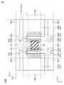
以下の説明においては、本実施の形態に係る集合基板120Aの構成の理解を容易とするために、複数の抵抗体22のうちの1つが設けられた製品予定領域Raと、当該製品予定領域Raを取り囲む部分である枠状領域とからなる図6中に示す単位領域VIIに着目して説明を行なう。 In the following description, in order to facilitate the understanding of the configuration of the
図6および図7に示されるように、抵抗体22のX軸方向における両隣には、略E字状の導電パターンである第1導電パターンP1と第2導電パターンP2とが位置している。第1導電パターンP1は、第1上面導体24Aとなる端子部(第1端子部)124Aと、抵抗値を測定するために用いられる電極部(第1電極部)125Aと、配線部126Aとを有している。第2導電パターンP2は、第2上面導体24Bとなる端子部(第2端子部)124Bと、抵抗値を測定するために用いられる電極部(第2電極部)125Bと、配線部126Bとを有している。 As shown in FIGS. 6 and 7, the first conductive pattern P1 and the second conductive pattern P2, which are substantially E-shaped conductive patterns, are located on both sides of the
ここで、端子部124Aおよび124Bは、いずれも製品予定領域Raに位置している。また、電極部125Aおよび125Bは、いずれも第1領域Rb1および第3領域Rb3に位置している。さらに、配線部126Aおよび126Bは、いずれも第2領域Rb2に位置している。なお、電極部125Aおよび電極部125Bの各々の面積は、端子部124Aおよび端子部124Bの面積のいずれよりも大きく、当該電極部125Aおよび電極部125Bが、上述した工程ST7における抵抗体のトリミングの際に抵抗計のプローブが押し付けられる部分となる。 Here, the
略矩形状の導電パターンの一方である第3導電パターンP3は、第3上面導体24Cとなるものであり、上述した第1導電パターンP1の端子部124Aと電極部125Aとの間に位置している。略矩形状の導電パターンの他方である第4導電パターンP4は、第4上面導体24Dとなるものであり、上述した第2導電パターンP2の端子部124Bと電極部125Bとの間に位置している。 The third conductive pattern P3 which is one of the substantially rectangular conductive patterns is to be the third
ここで、端子部124A、124Bは、X軸方向において離隔しており、これら端子部124A、124Bにその両端部が接続されるように、抵抗体22がX軸方向に沿って延在している。 Here, the
第1導電パターンP1、第2導電パターンP2、第3導電パターンP3および第4導電パターンP4をこのように配置することにより、製品予定領域Raにおいて、上述した抵抗素子20Aの上面20a上における第1上面導体24Aから第4上面導体24Dのレイアウトが実現される。あわせて、第1導電パターンP1および第2導電パターンP2のそれぞれの第3導電パターンP3および第4導電パターンP4に対する電気的な絶縁を維持しつつ、端子部124Aを電極部125Aに電気的に接続することが可能になるとともに、端子部124Bを電極部125Bに電気的に接続することが可能になる。 By arranging the first conductive pattern P1, the second conductive pattern P2, the third conductive pattern P3 and the fourth conductive pattern P4 in this manner, in the product planned region Ra, the first on the upper surface 20a of the
換言すれば、本実施の形態に係る集合基板120Aにあっては、抵抗体22に接続された端子部124Aは、Y軸方向に引き出されることで切除予定領域である枠状領域の第2領域Rb2に設けられた配線部126Aを経由して電極部125Aに電気的に接続されており、これによりX軸方向において電極部125Aと離隔している。同様に、抵抗体22に接続された端子部124Bは、Y軸方向に引き出されることで切除予定領域である枠状領域の第2領域Rb2に設けられた配線部126Bを経由して電極部125Bに電気的に接続されており、これによりX軸方向において電極部125Bと離隔している。 In other words, in the
このように構成された集合基板120Aにおいては、他のレイアウトを採用した場合に比べ、切除予定領域の大型化を抑制しつつ、抵抗素子20Aの取り個数を多く確保することができる。 In the
また、図6に示されるように、上記構成の集合基板120Aにあっては、X軸方向において隣り合う一対の製品予定領域Raのうちの一方の端子部に接続された電極部と、上記一対の製品予定領域Raのうちの他方の端子部に接続された電極部とが、共通化された単一の電極部にて構成されている。このように構成することにより、電極部を個別に設けた場合に比べて電極部の数が約半数に削減できるため、この点においても、切除予定領域の大型化を抑制しつつ、抵抗素子20Aの取り個数を多く確保することが可能になる。 Further, as shown in FIG. 6, in the
(実施の形態2)
図8は、本発明の実施の形態2に係る集合基板120Bの模式的な上面図であり、図9は、図8中に示す単位領域IXを拡大した模式的な上面図である。以下においては、これら図8および図9を参照して、本実施の形態に係る集合基板120Bについて説明する。なお、図8においては、上述した図6と同様に、保護膜の硬化処理後のマザー基板121の状態が表わされており、図9においては、上述した図7と同様に、抵抗体ペーストの焼き付け後のマザー基板121の状態が表わされている。Second Embodiment
FIG. 8 is a schematic top view of a
図8および図9に示されるように、本実施の形態に係る集合基板120Bは、上述した実施の形態1に係る集合基板120Aと比較した場合に、集合基板120Aが備えていた略矩形状の導電パターンが設けられていない点において相違している。 As shown in FIGS. 8 and 9, the
具体的には、図8に示されるように、マザー基板121の上面121aには、X軸方向における端部を除き、平面視された場合に略E字状である複数の導電パターン(第1導電パターンP1および第2導電パターンP2)と、複数の抵抗体22と、複数の保護膜23とのみが設けられている。複数の抵抗体22および複数の保護膜23は、それぞれ製品予定領域Raに設けられており、略E字状の導電パターンP1、P2は、それぞれ製品予定領域Raの一部ならびに枠状領域に含まれる一対の第1領域Rb1、一対の第2領域Rb2の一部および4つの第3領域Rb3の一部に連なって設けられている。 Specifically, as shown in FIG. 8, on the
以下の説明においては、本実施の形態に係る集合基板120Bの構成の理解を容易とするために、複数の抵抗体22のうちの1つが設けられた製品予定領域Raと、当該製品予定領域Raを取り囲む部分である枠状領域とからなる図8中に示す単位領域IXに着目して説明を行なう。 In the following description, in order to facilitate the understanding of the configuration of the
図8および図9に示されるように、抵抗体22のX軸方向における両隣には、略E字状の導電パターンである第1導電パターンP1と第2導電パターンP2とが位置している。第1導電パターンP1は、第1上面導体24Aとなる端子部(第1端子部)124Aと、抵抗値を測定するために用いられる電極部(第1電極部)125Aと、配線部126Aとを有している。第2導電パターンP2は、第2上面導体24Bとなる端子部(第2端子部)124Bと、抵抗値を測定するために用いられる電極部(第2電極部)125Bと、配線部126Bとを有している。 As shown in FIGS. 8 and 9, the first conductive pattern P1 and the second conductive pattern P2, which are substantially E-shaped conductive patterns, are located on both sides of the
ここで、電極部125Aおよび125Bは、いずれも第1領域Rb1、第3領域Rb3および製品予定領域Raに位置している。そして、電極部125Aのうちの製品予定領域Raに位置する部分は、第3上面導体となる第1部分124Cとなっている。同様に、電極部125Bのうちの製品予定領域Raに位置する部分は、第4上面導体となる第2部分124Dとなっている。すなわち、本実施の形態に係る集合基板120Bは、上述した実施の形態1に係る集合基板120Aが備えていた略矩形状の第3導電パターンP3および第4導電パターンP4を有しておらず、電極部125Aと端子部124AとがX軸方向において直接向き合っているとともに、電極部125Bと端子部124BとがX軸方向において直接向き合っている。 Here, the
このように第1導電パターンP1および第2導電パターンP2を配置することにより、製品予定領域Raにおいて、上述した抵抗素子20Aの上面20a上における第1上面導体24Aから第4上面導体24Dのレイアウトが実現されることになる。あわせて、端子部124Aを電極部125Aに電気的に接続することが可能になるとともに、端子部124Bを電極部125Bに電気的に接続することが可能になる。 By arranging the first conductive pattern P1 and the second conductive pattern P2 in this manner, the layout of the first
また、本実施の形態に係る集合基板120Bにあっては、電極部125Aが、当該電極部125Aが設けられた第1領域Rb1に隣接する一対の製品予定領域Raの双方に連なって設けられており、そのうちの一方の製品予定領域Raに位置する第1部分124Cが、一方の製品予定領域Raに対応する抵抗素子20Aの第3上面導体24Cとなり、そのうちの他方の製品予定領域Raに位置する第2部分124Dが、他方の製品予定領域Raに対応する抵抗素子20Aの第4上面導体24Dとなる。同様に、本実施の形態に係る集合基板120Bにあっては、電極部125Bが、当該電極部125Bが設けられた第1領域Rb1に隣接する一対の製品予定領域Raの双方に連なって設けられており、そのうちの一方の製品予定領域Raに位置する第2部分124Dが、一方の製品予定領域Raに対応する抵抗素子20Aの第4上面導体24Dとなり、そのうちの他方の製品予定領域Raに位置する第1部分124Cが、他方の製品予定領域Raに対応する抵抗素子20Aの第3上面導体24Cとなる。 In addition, in the
このように構成された集合基板120Bにおいては、上述した実施の形態1において説明した効果に加え、さらに切除予定領域を小さくすることができ、抵抗素子20Aの取り個数をさらに多く確保することができる。 In the
ここで、上記構成の集合基板120Bにあっては、端子部124Aとこれに配線部126Aを経由して接続された電極部125AとのX軸方向における間隔D1が、端子部124Aと端子部124BとのX軸方向における間隔D0よりも小さい(D1<D0)。また、同様に、端子部124Bとこれに配線部126Bを経由して接続された電極部125BとのX軸方向における間隔D2が、端子部124Aと端子部124BとのX軸方向における間隔D0よりも小さい(D2<D0)。 Here, in the
このように構成することにより、抵抗体22の面積が広がって抵抗体22の電気特性を調整するための自由度が高まることになるとともに、切除予定領域が大幅に小さくなる。なお、上述したD1<D0および/またはD2/D0の条件は、上述した実施の形態1の如くの導電パターンのレイアウトを採用した場合にも、その適用が可能である。 With such a configuration, the area of the
以上において示した本発明の実施の形態1および2においては、第1上面導体部および第2上面導体部からそれぞれY軸方向に沿って引き出される配線部が、いずれも同じ方向に向けて引き出されるように構成した場合を例示して説明を行なったが、後述する実施の形態3の場合のように、これら配線部をY軸方向に沿って互いに逆向きに引き出すことも当然に可能である。 In the first and second embodiments of the present invention described above, wiring portions drawn from the first upper surface conductor portion and the second upper surface conductor portion along the Y-axis direction are both drawn in the same direction. Although the case where it is configured as described above has been described as an example, as in the case of the third embodiment to be described later, it is naturally possible to draw these wiring portions in opposite directions along the Y-axis direction.
また、上述した本発明の実施の形態1および2においては、基部に埋め込み配線としての内部接続導体を形成するために、2層のセラミックグリーンシートを貼り合わせることで形成されたLTCC基板をマザー基板として採用した場合を例示して説明を行なったが、後述する実施の形態3の場合のように、埋め込み配線を有さない単層の基板をマザー基板として採用することも当然に可能である。 In the first and second embodiments of the present invention described above, in order to form the internal connection conductor as the embedded wiring in the base, the LTCC substrate formed by bonding two layers of ceramic green sheets is used as a mother substrate. Although the case where it adopted as is illustrated and demonstrated, of course, it is also possible to adopt the substrate of the single layer which does not have embedded wiring as a mother substrate like the case of Embodiment 3 mentioned later.
(実施の形態3)
図10は、本発明の実施の形態3に係る集合基板120C(図13および図14参照)を用いて製作された抵抗素子20Bを備える複合電子部品1Bの概略的な斜視図である。図11(A)および図11(B)は、それぞれ図10中に示されるXIA−XIA線およびXIB−XIB線に沿って複合電子部品1Bが切断された場合の模式的な断面図である。図12(A)および図12(B)は、それぞれ図10に示される抵抗素子20Bの模式的な上面図および下面図である。Third Embodiment
FIG. 10 is a schematic perspective view of a composite
まず、本実施の形態に係る集合基板120Cを説明するに先立って、図10から図12を参照して、当該集合基板120Cを用いて製作された抵抗素子20Bならびにこの抵抗素子20Bを備える複合電子部品1Bについて説明する。 First, prior to describing the collective substrate 120C according to the present embodiment, referring to FIG. 10 to FIG. 12, a
図10および図11に示されるように、複合電子部品1Bは、第1の電子素子としてコンデンサ素子10と、第2の電子素子として抵抗素子20Bとを備えている。 As shown in FIGS. 10 and 11, the composite
図10から図12に示されるように、抵抗素子20Bは、第1上面導体24A、第2上面導体24B、第1下面導体25Aおよび第2下面導体25Bの配設位置ならびに第1接続導体26Aおよび第2接続導体26Bの配設位置や構成において、上述した抵抗素子20Aと主として相違している。 As shown in FIGS. 10 to 12,
図11および図12、特に図12(A)に示されるように、第1上面導体24Aおよび第2上面導体24Bは、いずれも基部21の上面21aに設けられており、第1上面導体24Aおよび第2上面導体24Bの各々は、高さ方向Hに沿って抵抗素子20Bが平面視されたときに、長さ方向Lの寸法が幅方向Wの寸法よりも大きい矩形状に構成されている。 As shown in FIGS. 11 and 12, particularly in FIG. 12A, the first
第1上面導体24Aと第2上面導体24Bとは、基部21の中心を挟んで幅方向Wにおいて離隔しており、第1上面導体24Aは、基部21の幅方向Wに沿った第3側面側の端部に配置され、第2上面導体24Bは、基部21の幅方向Wに沿った第4側面側の端部に配置されている。ここで、第1上面導体24Aおよび第2上面導体24Bは、長さ方向Lにおいて第3上面導体24Cと第4上面導体24Dとの間に位置している。 The first
図11および図12、特に図12(B)に示されるように、第1下面導体25Aおよび第2下面導体25Bは、いずれも基部21の下面21bに設けられており、第1下面導体25Aおよび第2下面導体25Bの各々は、高さ方向Hに沿って抵抗素子20Bが平面視されたときに、長さ方向Lの寸法が幅方向Wの寸法よりも大きい矩形状に構成されている。 As shown in FIGS. 11 and 12, particularly in FIG. 12B, the first
第1下面導体25Aと第2下面導体25Bとは、基部21の中心を挟んで幅方向Wにおいて離隔しており、第1下面導体25Aは、基部21の幅方向Wに沿った第3側面側の端部に配置され、第2下面導体25Bは、基部21の幅方向Wに沿った第4側面側の端部に配置されている。ここで、第1下面導体25Aおよび第2下面導体25Bは、長さ方向Lにおいて第3下面導体25Cと第4下面導体25Dとの間に位置している。なお、第1下面導体25Aは、基部21を挟んで第1上面導体24Aと相対しており、第2下面導体25Bは、基部21を挟んで第2上面導体24Bと相対している。 The first
図11および図12に示されるように、基部21の内部には、第1接続導体26Aおよび第2接続導体26Bが設けられている。第1接続導体26Aは、基部21を高さ方向Hに貫通するビア導体にて構成されており、第1上面導体24Aと第1下面導体25Aとを接続している。第2接続導体26Bは、基部21を高さ方向Hに貫通するビア導体にて構成されており、第2上面導体24Bと第2下面導体25Bとを接続している。 As shown in FIGS. 11 and 12, a
図11および図12、特に図12(A)に示されるように、抵抗体22は、幅方向Wにおいて第1上面導体24Aが設けられた領域と第2上面導体24Bが設けられた領域との間に主として位置しており、高さ方向Hから平面視された場合に、抵抗体22の幅方向Wにおける一端が第1上面導体24Aの一部と重なっているとともに、抵抗体22の幅方向Wにおける他端が第2上面導体24Bの一部と重なっている。これにより、第1上面導体24Aおよび第2上面導体24Bが、抵抗体22に接続される。 As shown in FIGS. 11 and 12, particularly in FIG. 12A, in the width direction W, the
また、保護膜23は、基部21の上面21a上において抵抗体22、第1上面導体24Aの一部および第2上面導体24Bの一部を覆っている。 In addition, the
図13は、本実施の形態に係る集合基板120Cの模式的な上面図であり、図14は、図13中に示す単位領域XIVを拡大した模式的な上面図である。以下においては、これら図13および図14を参照して、本実施の形態に係る集合基板120Cについて説明する。なお、図13においては、上述した図6と同様に、保護膜の硬化処理後のマザー基板121の状態が表わされており、図14においては、上述した図7と同様に、抵抗体ペーストの焼き付け後のマザー基板121の状態が表わされている。 FIG. 13 is a schematic top view of a collective substrate 120C according to the present embodiment, and FIG. 14 is a schematic top view enlarging a unit region XIV shown in FIG. Hereinafter, a collective substrate 120C according to the present embodiment will be described with reference to FIGS. 13 and 14. 13 shows the state of
図13および図14に示されるように、本実施の形態に係る集合基板120Cは、上述した実施の形態2に係る集合基板120Bと比較した場合に、製品予定領域Raに設けられた端子部124Aおよび124Bの配設位置が異なっている。 As shown in FIGS. 13 and 14, when compared with the
具体的には、図13に示されるように、マザー基板121の上面121aには、X軸方向における端部を除き、平面視された場合に略S字状である複数の導電パターン(第1導電パターンP1および第2導電パターンP2)と、複数の抵抗体22と、複数の保護膜23とが設けられている。複数の抵抗体22および複数の保護膜23は、それぞれ製品予定領域Raに設けられており、略S字状の導電パターンP1、P2は、それぞれ製品予定領域Raの一部ならびに枠状領域に含まれる一対の第1領域Rb1、一対の第2領域Rb2の一部および4つの第3領域Rb3の一部に連なって設けられている。 Specifically, as shown in FIG. 13, the
以下の説明においては、本実施の形態に係る集合基板120Cの構成の理解を容易とするために、複数の抵抗体22のうちの1つが設けられた製品予定領域Raと、当該製品予定領域Raを取り囲む部分である枠状領域とからなる図13中に示す単位領域XIVに着目して説明を行なう。 In the following description, in order to facilitate the understanding of the configuration of the collective substrate 120C according to the present embodiment, a product planned area Ra in which one of the plurality of
図13および図14に示されるように、抵抗体22のX軸方向における両隣には、略S字状の導電パターンである第1導電パターンP1と第2導電パターンP2とが位置している。第1導電パターンP1は、第1上面導体24Aとなる端子部(第1端子部)124Aと、抵抗値を測定するために用いられる電極部(第1電極部)125Aと、配線部126Aとを有している。第2導電パターンP2は、第2上面導体24Bとなる端子部(第2端子部)124Bと、抵抗値を測定するために用いられる電極部(第2電極部)125Bと、配線部126Bとを有している。 As shown in FIGS. 13 and 14, the first conductive pattern P1 and the second conductive pattern P2, which are substantially S-shaped conductive patterns, are located on both sides of the
そして、電極部125Aのうちの製品予定領域Raに位置する部分は、第3上面導体となる第1部分124Cとなっている。同様に、電極部125Bのうちの製品予定領域Raに位置する部分は、第4上面導体となる第2部分124Dとなっている。 And the part located in product plan area Ra among
ここで、端子部124A、124Bは、Y軸方向において離隔しており、これら端子部124A、124Bにその両端部が接続されるように、抵抗体22がY軸方向に沿って延在している。 Here, the
このように構成した場合にも、上述した実施の形態2の場合と同様の効果を得ることができる。すなわち、製品予定領域Raにおいて、上述した抵抗素子20Bの上面20a上における第1上面導体24Aから第4上面導体24Dのレイアウトが実現されることになる。あわせて、端子部124Aを電極部125Aに電気的に接続することが可能になるとともに、端子部124Bを電極部125Bに電気的に接続することが可能になる。 Even when configured as described above, the same effects as those of the second embodiment described above can be obtained. That is, the layout of the first
なお、本実施の形態においては、第3上面導体となる第1部分124Cを電極部125Aに設けるとともに、第4上面導体となる第2部分124Dを電極部125Bに設けるように構成した場合を例示して説明を行なったが、これら第3上面導体および第4上面導体となる部分を、上述した実施の形態1において示したように、第1導電パターンP1および第2導電パターンP2と隔離された第3導電パターンP3および第4導電パターンP4にて構成することも当然に可能である。 In the present embodiment, the
以上において示した本発明の実施の形態1から3においては、個片化することで得られた抵抗素子をコンデンサ素子と一体化することで複合電子部品にすることが予定された集合基板を例示し、これに本発明を適用した場合を例示して説明を行なったが、当該抵抗素子に実装される電子素子は、当然にコンデンサ素子以外の電子素子、たとえばインダクタ素子やサーミスタ素子、圧電素子等であってもよい。 In the first to third embodiments of the present invention described above, the collective substrate intended to be a composite electronic component by integrating the resistive element obtained by singulation with the capacitor element is exemplified. Although the case where the present invention is applied is described as an example, the electronic element mounted on the resistance element is, of course, an electronic element other than the capacitor element, such as an inductor element, a thermistor element, a piezoelectric element, etc. It may be
このように、今回開示した上記実施の形態はすべての点で例示である。本発明は、上記実施の形態に限定して解釈されるべきものではなく、いわゆる均等の範囲を含むものである。 As described above, the above-described embodiment disclosed this time is an example in all respects. The present invention should not be construed as being limited to the above embodiment, and includes what is called an equivalent range.
1A,1B 複合電子部品、10 コンデンサ素子、11 コンデンサ本体、11a 下面、12 誘電体層、13 内部電極層、14A,14B 外部電極、20A,20B 抵抗素子、21 基部、21a 上面、21b 下面、22 抵抗体、22a 除去痕、23 保護膜、24A 第1上面導体、24B 第2上面導体、24C 第3上面導体、24D 第4上面導体、25A 第1下面導体、25B 第2下面導体、25C 第3下面導体、25D 第4下面導体、26A 第1接続導体、26A1 内部接続導体、26A2 上側ビア導体、26A3 下側ビア導体、26B 第2接続導体、26B1 内部接続導体、26B2 上側ビア導体、26B3 下側ビア導体、26C 第3接続導体、26D 第4接続導体、120A〜120C マザー基板、121 基部、121a 上面、124A,124B 端子部、124C 第1部分、124D 第2部分、125A,125B 電極部、126A,126B 配線部、CL1,CL2 切断線、P1 第1導電パターン、P2 第2導電パターン、P3 第3導電パターン、P4 第4導電パターン、Ra 製品予定領域、Rb 切除予定領域、Rb1 第1領域、Rb2 第2領域、Rb3 第3領域。 DESCRIPTION OF SYMBOLS 1A, 1B composite electronic component, 10 capacitor element, 11 capacitor main body, 11a lower surface, 12 dielectric layer, 13 internal electrode layer, 14A, 14B external electrode, 20A, 20B resistive element, 21 base, 21a upper surface, 21b lower surface, 22 Resistor, 22a removal mark, 23 protective film, 24A first upper surface conductor, 24B second upper surface conductor, 24C third upper surface conductor, 24D fourth upper surface conductor, 25A first lower surface conductor, 25B second lower surface conductor, 25C third Lower surface conductor, 25D Fourth lower surface conductor, 26A first connecting conductor, 26A1 internal connection conductor, 26A2 upper via conductor, 26A3 lower via conductor, 26B second connecting conductor, 26B1 internal connecting conductor, 26B2 upper via conductor, 26B3 lower side Via conductor, 26C third connecting conductor, 26D fourth connecting conductor, 120A to 120C mother Plate, 121 base, 121a upper surface, 124A, 124B terminal portion, 124C first portion, 124D second portion, 125A, 125B electrode portion, 126A, 126B wiring portion, CL1, CL2 cutting line, P1 first conductive pattern, P2 first 2 conductive pattern, P3 third conductive pattern, P4 fourth conductive pattern, Ra product planned area, Rb planned area, Rb1 first area, Rb2 second area, Rb3 third area.
Claims (11)
Translated fromJapanese前記基部の上面に設けられた複数の抵抗体と、
前記基部の前記上面に設けられた複数の第1導電パターンとを備え、
前記複数の抵抗体の各々は、前記複数の製品予定領域のそれぞれに設けられ、
前記複数の製品予定領域のうちの1つの製品予定領域と、前記切除予定領域のうちの前記1つの製品予定領域を取り囲む部分である枠状領域とからなる部分を単位領域として、前記複数の第1導電パターンの各々は、複数存する前記単位領域のそれぞれに設けられ、
前記複数の単位領域の各々において、前記枠状領域は、前記複数の製品予定領域が並ぶ方向である行方向および列方向のうちの一方である第1方向において前記製品予定領域に隣接する第1領域と、前記行方向および前記列方向のうちの他方である第2方向において前記製品予定領域に隣接する第2領域とを含み、
前記複数の単位領域の各々において、前記第1導電パターンは、前記抵抗体に接続されるとともに前記製品予定領域に配設された第1端子部と、前記第1領域に少なくとも配設されるとともに前記第1端子部よりも面積が大きい第1電極部と、前記第1端子部から前記第2領域に向けて引き出されるとともに前記枠状領域のみを経由して前記第1電極部に接続された第1配線部とを有している、抵抗素子用の集合基板。A base including a plurality of product planned areas spaced apart from one another in a matrix and a grid-like planned cutting area located between the plurality of product planned areas;
A plurality of resistors provided on the upper surface of the base;
And a plurality of first conductive patterns provided on the upper surface of the base,
Each of the plurality of resistors is provided in each of the plurality of product planned areas,
A plurality of parts each including a product planned area of the plurality of product planned areas and a frame-like area which is a part surrounding the one product planned area of the ablation planned areas is a unit area. Each of the one conductive patterns is provided in each of the plurality of unit areas existing,
In each of the plurality of unit areas, the frame-like area is adjacent to the product planned area in a first direction which is one of a row direction and a column direction in which the plurality of product planned areas are arranged. A region, and a second region adjacent to the product planned region in a second direction which is the other of the row direction and the column direction,
In each of the plurality of unit regions, the first conductive pattern is at least provided in the first region connected to the resistor and disposed in the product planned region, and in the first region. A first electrode portion having a larger area than the first terminal portion and a first electrode portion drawn from the first terminal portion toward the second region and connected to the first electrode portion only via the frame-like region A collective substrate for a resistive element, having a first wiring portion.
前記複数の第2導電パターンの各々は、複数存する前記単位領域のそれぞれに設けられ、
前記複数の単位領域の各々において、前記第2導電パターンは、前記抵抗体に接続されるとともに前記製品予定領域に配設された第2端子部と、前記第1領域に少なくとも配設されるとともに前記第2端子部よりも面積が大きい第2電極部と、前記第2端子部から前記第2領域に向けて引き出されるとともに前記枠状領域のみを経由して前記第2電極部に接続された第2配線部とを有している、請求項1に記載の抵抗素子用の集合基板。And a plurality of second conductive patterns provided on the top surface of the base and separated from each of the plurality of first conductive patterns;
Each of the plurality of second conductive patterns is provided in each of the plurality of unit regions,
In each of the plurality of unit regions, the second conductive pattern is at least disposed in the first region connected to the resistor and disposed in the first region. A second electrode portion having a larger area than the second terminal portion, and the second electrode portion is drawn out from the second terminal portion toward the second region and connected to the second electrode portion only via the frame-like region. The aggregate substrate for a resistance element according to claim 1, comprising: a second wiring portion.
前記複数の単位領域の各々において、前記第1部分が、前記第1方向において前記第1端子部と離隔し、かつ、前記第2部分が、前記第1方向において前記第2端子部と離隔している、請求項3に記載の抵抗素子用の集合基板。In each of the plurality of unit regions, the first electrode portion includes a first portion connected to the portion disposed in the first region and disposed in the product planned region, and the second electrode A part is connected to the part disposed in the first area and includes a second part disposed in the product planned area;
In each of the plurality of unit regions, the first portion is separated from the first terminal portion in the first direction, and the second portion is separated from the second terminal portion in the first direction. The collective substrate for resistive elements according to claim 3.
前記基部の前記上面に設けられ、前記複数の第1導電パターンの各々および前記複数の第2導電パターンの各々から離隔した複数の第4導電パターンとをさらに備え、
前記複数の第3導電パターンの各々は、複数存する前記単位領域のそれぞれに設けられ、
前記複数の第4導電パターンの各々は、複数存する前記単位領域のそれぞれに設けられ、
前記複数の単位領域の各々において、前記第3導電パターンが、前記第1端子部と前記第1電極部との間に位置する部分の前記製品予定領域に配設され、かつ、前記第4導電パターンが、前記第2端子部と前記第2電極部との間に位置する部分の前記製品予定領域に配設されている、請求項3に記載の抵抗素子用の集合基板。A plurality of third conductive patterns provided on the top surface of the base and separated from each of the plurality of first conductive patterns and each of the plurality of second conductive patterns;
And a plurality of fourth conductive patterns provided on the upper surface of the base and separated from each of the plurality of first conductive patterns and each of the plurality of second conductive patterns.
Each of the plurality of third conductive patterns is provided in each of the plurality of unit regions,
Each of the plurality of fourth conductive patterns is provided in each of the plurality of unit regions,
In each of the plurality of unit areas, the third conductive pattern is disposed in the product planned area of a portion positioned between the first terminal portion and the first electrode portion, and the fourth conductive portion The aggregate substrate for a resistance element according to claim 3, wherein a pattern is disposed in the product planned area of a portion located between the second terminal portion and the second electrode portion.
前記複数の単位領域の各々において、前記第1部分が、前記第1方向において前記第1端子部と離隔し、かつ、前記第2部分が、前記第1方向において前記第2端子部と離隔している、請求項7に記載の抵抗素子用の集合基板。In each of the plurality of unit regions, the first electrode portion includes a first portion connected to the portion disposed in the first region and disposed in the product planned region, and the second electrode A part is connected to the part disposed in the first area and includes a second part disposed in the product planned area;
In each of the plurality of unit regions, the first portion is separated from the first terminal portion in the first direction, and the second portion is separated from the second terminal portion in the first direction. The collective substrate for resistive elements according to claim 7.
前記基部の前記上面に設けられ、前記複数の第1導電パターンの各々および前記複数の第2導電パターンの各々から離隔した複数の第4導電パターンとをさらに備え、
前記複数の第3導電パターンの各々は、複数存する前記単位領域のそれぞれに設けられ、
前記複数の第4導電パターンの各々は、複数存する前記単位領域のそれぞれに設けられ、
前記複数の単位領域の各々において、前記第3導電パターンが、前記第1端子部と前記第1電極部との間に位置する部分の前記製品予定領域に配設され、かつ、前記第4導電パターンが、前記第2端子部と前記第2電極部との間に位置する部分の前記製品予定領域に配設されている、請求項7に記載の抵抗素子用の集合基板。A plurality of third conductive patterns provided on the top surface of the base and separated from each of the plurality of first conductive patterns and each of the plurality of second conductive patterns;
And a plurality of fourth conductive patterns provided on the upper surface of the base and separated from each of the plurality of first conductive patterns and each of the plurality of second conductive patterns.
Each of the plurality of third conductive patterns is provided in each of the plurality of unit regions,
Each of the plurality of fourth conductive patterns is provided in each of the plurality of unit regions,
In each of the plurality of unit areas, the third conductive pattern is disposed in the product planned area of a portion positioned between the first terminal portion and the first electrode portion, and the fourth conductive portion The aggregate substrate for a resistance element according to claim 7, wherein a pattern is disposed in the product planned area of a portion located between the second terminal portion and the second electrode portion.
前記複数の保護膜の各々は、前記複数の製品予定領域のそれぞれに設けられ、
前記複数の単位領域の各々において、前記保護膜は、前記抵抗体と、前記第1端子部の少なくとも一部と、前記第2端子部の少なくとも一部とを覆っている、請求項2から10のいずれかに記載の抵抗素子用の集合基板。It further comprises a plurality of protective films provided on the upper surface of the base,
Each of the plurality of protective films is provided in each of the plurality of product planned areas,
The protective film covers each of the plurality of unit regions, at least a portion of the first terminal portion, and at least a portion of the second terminal portion. A collective substrate for the resistive element according to any one of the above.
Priority Applications (4)
| Application Number | Priority Date | Filing Date | Title |
|---|---|---|---|
| JP2015166914AJP6500700B2 (en) | 2015-08-26 | 2015-08-26 | Integrated substrate for resistive elements |
| US15/239,943US9832877B2 (en) | 2015-08-26 | 2016-08-18 | Collective substrate for resistor devices |
| KR1020160105987AKR101973368B1 (en) | 2015-08-26 | 2016-08-22 | Collective substrate for resistor devices |
| CN201610718840.0ACN106486223B (en) | 2015-08-26 | 2016-08-24 | The assembly substrate of resistive element |
Applications Claiming Priority (1)
| Application Number | Priority Date | Filing Date | Title |
|---|---|---|---|
| JP2015166914AJP6500700B2 (en) | 2015-08-26 | 2015-08-26 | Integrated substrate for resistive elements |
Publications (2)
| Publication Number | Publication Date |
|---|---|
| JP2017045848A JP2017045848A (en) | 2017-03-02 |
| JP6500700B2true JP6500700B2 (en) | 2019-04-17 |
Family
ID=58096423
Family Applications (1)
| Application Number | Title | Priority Date | Filing Date |
|---|---|---|---|
| JP2015166914AActiveJP6500700B2 (en) | 2015-08-26 | 2015-08-26 | Integrated substrate for resistive elements |
Country Status (4)
| Country | Link |
|---|---|
| US (1) | US9832877B2 (en) |
| JP (1) | JP6500700B2 (en) |
| KR (1) | KR101973368B1 (en) |
| CN (1) | CN106486223B (en) |
Families Citing this family (4)
| Publication number | Priority date | Publication date | Assignee | Title |
|---|---|---|---|---|
| JP6582648B2 (en)* | 2015-07-10 | 2019-10-02 | 株式会社村田製作所 | Composite electronic components |
| JP6503943B2 (en)* | 2015-07-10 | 2019-04-24 | 株式会社村田製作所 | Composite electronic component and resistor |
| US11020966B2 (en)* | 2018-04-27 | 2021-06-01 | Canon Kabushiki Kaisha | Liquid ejection head substrate, method of manufacturing liquid ejection head substrate, and liquid ejection head |
| EP4187172A1 (en)* | 2021-11-25 | 2023-05-31 | BorgWarner Inc. | Method for confectioning resistors, resistor, and heating device |
Family Cites Families (18)
| Publication number | Priority date | Publication date | Assignee | Title |
|---|---|---|---|---|
| JPS60158651A (en)* | 1984-01-27 | 1985-08-20 | Nippon Abionikusu Kk | Manufacture of hybrid integrated circuit |
| JPS6291475U (en)* | 1985-11-28 | 1987-06-11 | ||
| JPS63133657A (en)* | 1986-11-26 | 1988-06-06 | Nec Corp | Hybrid integrated circuit device |
| JPH0484491A (en)* | 1990-07-27 | 1992-03-17 | Nec Corp | Thick printed wiring board and its manufacture |
| JPH06283301A (en) | 1993-03-29 | 1994-10-07 | Mitsubishi Materials Corp | Composite chip electronic parts and their manufacture |
| JPH0992512A (en)* | 1995-09-25 | 1997-04-04 | Rohm Co Ltd | Chip-type composite electronic component and manufacturing method thereof |
| JPH11340002A (en) | 1998-05-26 | 1999-12-10 | Rohm Co Ltd | Assembled substrate for chip type resistor |
| JP4504075B2 (en)* | 2004-04-15 | 2010-07-14 | 釜屋電機株式会社 | Collective substrate for electronic component and method for manufacturing electronic component |
| WO2009087937A1 (en)* | 2008-01-08 | 2009-07-16 | Alps Electric Co., Ltd. | Magnetic sensor and magnetic encoder |
| JP5032351B2 (en)* | 2008-01-25 | 2012-09-26 | Tdk株式会社 | Barista |
| EP2267413B1 (en)* | 2008-03-25 | 2016-10-19 | Alps Electric Co., Ltd. | Magnetic sensor and magnetic encoder |
| CN101978490B (en)* | 2008-03-31 | 2012-10-17 | 株式会社村田制作所 | Electronic component assembly and method for manufacturing the electronic component assembly |
| JP5360425B2 (en)* | 2010-04-08 | 2013-12-04 | 株式会社村田製作所 | Circuit module and method of manufacturing circuit module |
| JP5778690B2 (en)* | 2010-11-22 | 2015-09-16 | Tdk株式会社 | Chip thermistor and thermistor assembly board |
| WO2013065420A1 (en)* | 2011-10-31 | 2013-05-10 | 株式会社村田製作所 | Electronic component, assembly substrate, and method for manufacturing electronic component |
| JP5285819B1 (en)* | 2012-11-07 | 2013-09-11 | 太陽誘電株式会社 | Electronic circuit module |
| JP6554833B2 (en)* | 2015-03-12 | 2019-08-07 | 株式会社村田製作所 | Composite electronic components and resistive elements |
| JP2017005221A (en)* | 2015-06-16 | 2017-01-05 | 株式会社村田製作所 | Composite electronic component |
- 2015
- 2015-08-26JPJP2015166914Apatent/JP6500700B2/enactiveActive
- 2016
- 2016-08-18USUS15/239,943patent/US9832877B2/enactiveActive
- 2016-08-22KRKR1020160105987Apatent/KR101973368B1/enactiveActive
- 2016-08-24CNCN201610718840.0Apatent/CN106486223B/enactiveActive
Also Published As
| Publication number | Publication date |
|---|---|
| US20170064834A1 (en) | 2017-03-02 |
| KR20170026158A (en) | 2017-03-08 |
| CN106486223A (en) | 2017-03-08 |
| KR101973368B1 (en) | 2019-04-29 |
| US9832877B2 (en) | 2017-11-28 |
| CN106486223B (en) | 2018-12-18 |
| JP2017045848A (en) | 2017-03-02 |
Similar Documents
| Publication | Publication Date | Title |
|---|---|---|
| JP6554833B2 (en) | Composite electronic components and resistive elements | |
| US10418183B2 (en) | Composite electronic component and resistor device | |
| US10121593B2 (en) | Composite electronic component | |
| US10453617B2 (en) | Composite electronic component and resistance element | |
| US10299383B2 (en) | Composite electronic component and resistance element | |
| KR101815443B1 (en) | Composite electronic component and resistance element | |
| US7417196B2 (en) | Multilayer board with built-in chip-type electronic component and manufacturing method thereof | |
| JP6500700B2 (en) | Integrated substrate for resistive elements | |
| US10319531B2 (en) | Composite electronic component and resistor device | |
| JP6984688B2 (en) | Composite electronic components | |
| JPH06204075A (en) | High frequency monolithic ceramic electronic component and manufacturing method thereof | |
| JP5981389B2 (en) | Wiring board | |
| JP2006216709A (en) | Multilayer wiring board incorporating multilayer electronic component and multilayer electronic component | |
| KR20060124834A (en) | Integrated Passive Chip and its Manufacturing Method | |
| JP2018041931A (en) | Composite electronic component |
Legal Events
| Date | Code | Title | Description |
|---|---|---|---|
| A621 | Written request for application examination | Free format text:JAPANESE INTERMEDIATE CODE: A621 Effective date:20180510 | |
| TRDD | Decision of grant or rejection written | ||
| A01 | Written decision to grant a patent or to grant a registration (utility model) | Free format text:JAPANESE INTERMEDIATE CODE: A01 Effective date:20190219 | |
| A977 | Report on retrieval | Free format text:JAPANESE INTERMEDIATE CODE: A971007 Effective date:20190228 | |
| A61 | First payment of annual fees (during grant procedure) | Free format text:JAPANESE INTERMEDIATE CODE: A61 Effective date:20190304 | |
| R150 | Certificate of patent or registration of utility model | Ref document number:6500700 Country of ref document:JP Free format text:JAPANESE INTERMEDIATE CODE: R150 |