JP6494184B2 - Thin film transistor, active matrix substrate, method for manufacturing thin film transistor, and method for manufacturing active matrix substrate - Google Patents
Thin film transistor, active matrix substrate, method for manufacturing thin film transistor, and method for manufacturing active matrix substrateDownload PDFInfo
- Publication number
- JP6494184B2 JP6494184B2JP2014121162AJP2014121162AJP6494184B2JP 6494184 B2JP6494184 B2JP 6494184B2JP 2014121162 AJP2014121162 AJP 2014121162AJP 2014121162 AJP2014121162 AJP 2014121162AJP 6494184 B2JP6494184 B2JP 6494184B2
- Authority
- JP
- Japan
- Prior art keywords
- film
- oxide
- oxide semiconductor
- conductive film
- electrode
- Prior art date
- Legal status (The legal status is an assumption and is not a legal conclusion. Google has not performed a legal analysis and makes no representation as to the accuracy of the status listed.)
- Active
Links
Images


Classifications
- H—ELECTRICITY
- H10—SEMICONDUCTOR DEVICES; ELECTRIC SOLID-STATE DEVICES NOT OTHERWISE PROVIDED FOR
- H10D—INORGANIC ELECTRIC SEMICONDUCTOR DEVICES
- H10D30/00—Field-effect transistors [FET]
- H10D30/60—Insulated-gate field-effect transistors [IGFET]
- H10D30/67—Thin-film transistors [TFT]
- H10D30/6729—Thin-film transistors [TFT] characterised by the electrodes
- H—ELECTRICITY
- H10—SEMICONDUCTOR DEVICES; ELECTRIC SOLID-STATE DEVICES NOT OTHERWISE PROVIDED FOR
- H10D—INORGANIC ELECTRIC SEMICONDUCTOR DEVICES
- H10D30/00—Field-effect transistors [FET]
- H10D30/60—Insulated-gate field-effect transistors [IGFET]
- H10D30/67—Thin-film transistors [TFT]
- H10D30/674—Thin-film transistors [TFT] characterised by the active materials
- H10D30/6755—Oxide semiconductors, e.g. zinc oxide, copper aluminium oxide or cadmium stannate
- H—ELECTRICITY
- H10—SEMICONDUCTOR DEVICES; ELECTRIC SOLID-STATE DEVICES NOT OTHERWISE PROVIDED FOR
- H10D—INORGANIC ELECTRIC SEMICONDUCTOR DEVICES
- H10D30/00—Field-effect transistors [FET]
- H10D30/60—Insulated-gate field-effect transistors [IGFET]
- H10D30/67—Thin-film transistors [TFT]
- H10D30/6757—Thin-film transistors [TFT] characterised by the structure of the channel, e.g. transverse or longitudinal shape or doping profile
- H—ELECTRICITY
- H10—SEMICONDUCTOR DEVICES; ELECTRIC SOLID-STATE DEVICES NOT OTHERWISE PROVIDED FOR
- H10D—INORGANIC ELECTRIC SEMICONDUCTOR DEVICES
- H10D64/00—Electrodes of devices having potential barriers
- H10D64/60—Electrodes characterised by their materials
- H10D64/62—Electrodes ohmically coupled to a semiconductor
- H—ELECTRICITY
- H10—SEMICONDUCTOR DEVICES; ELECTRIC SOLID-STATE DEVICES NOT OTHERWISE PROVIDED FOR
- H10D—INORGANIC ELECTRIC SEMICONDUCTOR DEVICES
- H10D86/00—Integrated devices formed in or on insulating or conducting substrates, e.g. formed in silicon-on-insulator [SOI] substrates or on stainless steel or glass substrates
- H10D86/40—Integrated devices formed in or on insulating or conducting substrates, e.g. formed in silicon-on-insulator [SOI] substrates or on stainless steel or glass substrates characterised by multiple TFTs
- H10D86/421—Integrated devices formed in or on insulating or conducting substrates, e.g. formed in silicon-on-insulator [SOI] substrates or on stainless steel or glass substrates characterised by multiple TFTs having a particular composition, shape or crystalline structure of the active layer
- H10D86/423—Integrated devices formed in or on insulating or conducting substrates, e.g. formed in silicon-on-insulator [SOI] substrates or on stainless steel or glass substrates characterised by multiple TFTs having a particular composition, shape or crystalline structure of the active layer comprising semiconductor materials not belonging to the Group IV, e.g. InGaZnO
- H—ELECTRICITY
- H10—SEMICONDUCTOR DEVICES; ELECTRIC SOLID-STATE DEVICES NOT OTHERWISE PROVIDED FOR
- H10D—INORGANIC ELECTRIC SEMICONDUCTOR DEVICES
- H10D86/00—Integrated devices formed in or on insulating or conducting substrates, e.g. formed in silicon-on-insulator [SOI] substrates or on stainless steel or glass substrates
- H10D86/40—Integrated devices formed in or on insulating or conducting substrates, e.g. formed in silicon-on-insulator [SOI] substrates or on stainless steel or glass substrates characterised by multiple TFTs
- H10D86/441—Interconnections, e.g. scanning lines
- H10D86/443—Interconnections, e.g. scanning lines adapted for preventing breakage, peeling or short circuiting
- H—ELECTRICITY
- H10—SEMICONDUCTOR DEVICES; ELECTRIC SOLID-STATE DEVICES NOT OTHERWISE PROVIDED FOR
- H10D—INORGANIC ELECTRIC SEMICONDUCTOR DEVICES
- H10D86/00—Integrated devices formed in or on insulating or conducting substrates, e.g. formed in silicon-on-insulator [SOI] substrates or on stainless steel or glass substrates
- H10D86/40—Integrated devices formed in or on insulating or conducting substrates, e.g. formed in silicon-on-insulator [SOI] substrates or on stainless steel or glass substrates characterised by multiple TFTs
- H10D86/60—Integrated devices formed in or on insulating or conducting substrates, e.g. formed in silicon-on-insulator [SOI] substrates or on stainless steel or glass substrates characterised by multiple TFTs wherein the TFTs are in active matrices
- H—ELECTRICITY
- H10—SEMICONDUCTOR DEVICES; ELECTRIC SOLID-STATE DEVICES NOT OTHERWISE PROVIDED FOR
- H10D—INORGANIC ELECTRIC SEMICONDUCTOR DEVICES
- H10D99/00—Subject matter not provided for in other groups of this subclass
Landscapes
- Thin Film Transistor (AREA)
- Electrodes Of Semiconductors (AREA)
Description
Translated fromJapanese本発明は、液晶ディスプレイ装置もしくは有機EL(electroluminescence)ディスプレイ装置などの電気光学表示装置、または半導体部品などに用いられる薄膜トランジスタおよびそれを備えるアクティブマトリックス基板、ならびに薄膜トランジスタの製造方法およびアクティブマトリックス基板の製造方法に関する。 The present invention relates to a thin film transistor used for an electro-optic display device such as a liquid crystal display device or an organic EL (electroluminescence) display device, or a semiconductor component, an active matrix substrate including the thin film transistor, a method for manufacturing the thin film transistor, and a method for manufacturing the active matrix substrate. About.
半導体装置の一例として、薄膜トランジスタ(Thin Film Transistor;略称:TFT)をスイッチング素子として用いたTFTアクティブマトリックス基板を備えたディスプレイ装置用の電気光学表示装置がある。この電気光学表示装置は、低消費電力および薄型という特徴を活かして、CRT(Cathode Ray Tube)に代わるフラットパネルディスプレイの一つとして製品への応用が盛んになされている。 As an example of a semiconductor device, there is an electro-optic display device for a display device including a TFT active matrix substrate using a thin film transistor (abbreviation: TFT) as a switching element. This electro-optic display device is actively applied to products as one of flat panel displays replacing CRT (Cathode Ray Tube) by utilizing the features of low power consumption and thinness.
このような半導体装置では、低コスト化が要求されている。従来、TFTには、製造工程の簡略化のために、アモルファスシリコン(Si)を半導体の活性層に用いた逆スタガ構造が主に採用されている。逆スタガ構造は、バックチャネルエッチング型またはバックチャネルエッチ型と呼ばれる。 In such a semiconductor device, cost reduction is required. Conventionally, in order to simplify the manufacturing process, an inverted stagger structure in which amorphous silicon (Si) is used as an active layer of a semiconductor has been mainly used for TFTs. The inverted staggered structure is called a back channel etching type or a back channel etching type.
従来のアモルファスシリコンよりも高い移動度を有する酸化物半導体を活性層に用いたTFT(以下「酸化物TFT」という場合がある)の開発が盛んになされている(たとえば、特許文献1,2および非特許文献1参照)。酸化物半導体としては、主に酸化亜鉛(ZnO)系、またはこれに酸化ガリウム(Ga2O3)および酸化インジウム(In2O3)を添加したInGaZnO系が主に用いられている。TFTs using an oxide semiconductor having higher mobility than conventional amorphous silicon as an active layer (hereinafter sometimes referred to as “oxide TFT”) have been actively developed (for example, Patent Documents 1 and 2 and Non-patent document 1). As an oxide semiconductor, a zinc oxide (ZnO) system or an InGaZnO system in which gallium oxide (Ga2 O3 ) and indium oxide (In2 O3 ) are added is mainly used.
従来から透光性導電膜としては、酸化インジウムIn2O3と酸化錫SnO2との化合物である酸化インジウム錫(Indium Tin Oxide;略称:ITO)で構成されるITO膜、および酸化インジウムIn2O3と酸化亜鉛ZnOとの化合物である酸化インジウム亜鉛(Indium Zinc Oxide;略称:IZO)で構成されるIZO膜などの酸化物導電膜が知られている。Conventionally, as a translucent conductive film, an ITO film made of indium tin oxide (abbreviation: ITO), which is a compound of indium oxide In2 O3 and tin oxide SnO2 , and indium oxide In2 are used. An oxide conductive film such as an IZO film made of indium zinc oxide (abbreviation: IZO) which is a compound of O3 and zinc oxide ZnO is known.
これらの酸化物導電膜と同様に、前述の酸化物半導体で構成される酸化物半導体膜は、フォトレジストのアルカリ系現像液に不溶であるとともに、シュウ酸およびカルボン酸などの弱酸系溶液でエッチングすることが可能である。したがって、薬液を用いた方法であるウエットエッチング法でパターン加工が容易であるという利点がある。 Like these oxide conductive films, the oxide semiconductor film composed of the above-described oxide semiconductor is insoluble in an alkaline developer of photoresist and etched with a weak acid solution such as oxalic acid and carboxylic acid. Is possible. Therefore, there is an advantage that pattern processing is easy by the wet etching method which is a method using a chemical solution.
しかし、前述の酸化物半導体膜は、TFTのソース電極およびドレイン電極となる金属膜、たとえばクロム(Cr)、チタン(Ti)、モリブデン(Mo)、タンタル(Ta)もしくはアルミニウム(Al)、またはこれらの合金から成る金属膜をエッチング加工するときに用いられる、公知の酸系溶液にも容易に溶けてしまう。 However, the above-described oxide semiconductor film is a metal film that becomes a source electrode and a drain electrode of a TFT, such as chromium (Cr), titanium (Ti), molybdenum (Mo), tantalum (Ta), or aluminum (Al), or these It is easily dissolved in a known acid solution used when etching a metal film made of the above alloy.
したがって、酸化物半導体膜を活性層に用いた酸化物TFTを製造する場合には、ソース電極およびドレイン電極となる金属膜のみをエッチングし、酸化物半導体膜をエッチングせずに残すような選択エッチングが可能となるように、金属膜、金属膜のエッチング溶液、および酸化物半導体膜の種類が選択される(たとえば、特許文献3参照)。 Therefore, when manufacturing an oxide TFT using an oxide semiconductor film as an active layer, selective etching is performed so that only the metal film to be a source electrode and a drain electrode is etched and the oxide semiconductor film is left without being etched. Therefore, the metal film, the etching solution for the metal film, and the type of the oxide semiconductor film are selected (see, for example, Patent Document 3).
また、酸化物TFTを低コストで製造するための技術が、たとえば特許文献4に開示されている。特許文献4には、活性層となる半導体膜の加工プロセスと、ソース電極およびドレイン電極となる金属膜の加工プロセスと、ソース電極およびドレイン電極と酸化物半導体膜との接続界面に形成したオーミックコンタクト層を分離する加工プロセスとを、ハーフトーンマスクを用いて1回のマスク工程によって製造する方法が開示されている。 Further, for example, Patent Document 4 discloses a technique for manufacturing an oxide TFT at a low cost. Patent Document 4 discloses a process for processing a semiconductor film serving as an active layer, a process for processing a metal film serving as a source electrode and a drain electrode, and an ohmic contact formed at a connection interface between the source electrode and drain electrode and the oxide semiconductor film. A method of manufacturing a processing process for separating layers by a single mask process using a halftone mask is disclosed.
特許文献4に開示される技術では、前述の加工プロセスを全てウエットエッチングによって行い、端面をテーパー形状に加工している。このときのウエットエッチングは、エッチング液として、燐酸と酢酸と硝酸との混合液、過酸化水素とアンモニアと水との混合液、および市販のシュウ酸系のエッチング液であるITO07N(関東化学株式会社製)を適宜使い分けて行われている。 In the technique disclosed in Patent Document 4, all the above-described processing processes are performed by wet etching, and the end surface is processed into a tapered shape. In this case, the wet etching is performed using, as an etching solution, a mixed solution of phosphoric acid, acetic acid and nitric acid, a mixed solution of hydrogen peroxide, ammonia and water, and ITO07N (Kanto Chemical Co., Ltd.) which is a commercially available oxalic acid-based etching solution. Manufactured) is used properly.
従来のアモルファスシリコン(Si)を半導体の活性層に用いる場合には、ドライエッチングによってパターン加工を行うので、半導体パターンの端面である側壁の断面形状をなだらかな傾斜状に加工する、いわゆるテーパー加工が容易である。 When conventional amorphous silicon (Si) is used for a semiconductor active layer, pattern processing is performed by dry etching. Therefore, a so-called taper processing is performed in which a cross-sectional shape of a side wall, which is an end surface of a semiconductor pattern, is processed into a gentle slope. Easy.
これに対し、酸化物半導体膜を半導体の活性層に用いる場合には、ウエットエッチングによってパターン加工が行われる。ウエットエッチングは、等方性エッチングであるので、パターンニングされた酸化物半導体の側壁は、ほぼ垂直となる。 On the other hand, when an oxide semiconductor film is used for a semiconductor active layer, pattern processing is performed by wet etching. Since wet etching is isotropic etching, the sidewalls of the patterned oxide semiconductor are almost vertical.
したがって、酸化物半導体膜の上に形成される膜のカバレッジ不良を引き起こす原因となっている。たとえば、TFT構造において、酸化物半導体膜のパターンの側壁を覆うように形成されたソース電極およびドレイン電極、ならびにこれらの配線の側壁でのステップカバレッジ特性が悪くなり、配線膜の断線などの問題が生じる。さらには、その上に形成される保護絶縁膜のステップカバレッジ特性も悪化させるという問題が生じる。 Therefore, it causes a poor coverage of a film formed over the oxide semiconductor film. For example, in a TFT structure, the source and drain electrodes formed so as to cover the sidewalls of the oxide semiconductor film pattern, and the step coverage characteristics at the sidewalls of these wirings deteriorate, and problems such as disconnection of the wiring film occur. Arise. Furthermore, there arises a problem that the step coverage characteristic of the protective insulating film formed thereon is also deteriorated.
さらに、TFTのソース電極およびドレイン電極を、アルミニウム(Al)、チタン(Ti)、クロム(Cr)、銅(Cu)、モリブデン(Mo)、タンタル(Ta)、タングステン(W)などの金属膜またはこれらの合金などで形成する場合には、ソース電極およびドレイン電極と酸化物半導体膜との電気的接合部において、界面の良好な電気特性を安定的に得るのが難しいという問題がある。また、界面での電気抵抗の増大によって、高い移動度を有する酸化物半導体の性能を充分に発揮することができないという問題がある。 Furthermore, the source electrode and drain electrode of the TFT are made of a metal film such as aluminum (Al), titanium (Ti), chromium (Cr), copper (Cu), molybdenum (Mo), tantalum (Ta), tungsten (W), or the like. In the case of using such an alloy or the like, there is a problem that it is difficult to stably obtain good electrical characteristics of the interface at the electrical junction between the source and drain electrodes and the oxide semiconductor film. In addition, there is a problem in that the performance of an oxide semiconductor having high mobility cannot be sufficiently exhibited due to an increase in electrical resistance at the interface.
これらの問題を解決するための技術として、前述の特許文献4には、酸化物半導体膜とオーミックコンタクト層とソース電極およびドレイン電極のパターンとによって形成される端面である側壁を、ウエットエッチングによってテーパー加工する技術が開示されている。 As a technique for solving these problems, the above-mentioned Patent Document 4 discloses that the side wall, which is an end face formed by the oxide semiconductor film, the ohmic contact layer, and the pattern of the source electrode and the drain electrode, is tapered by wet etching. Techniques for processing are disclosed.
しかし、特許文献4には、テーパー加工するためのポイントとなる具体的なウエットエッチング方法、条件などが開示されていない。特に、多層膜のパターニング加工に関して、ドライエッチングを用いたテーパー加工と異なり、ウエットエッチングを用いたテーパー加工においては、庇構造(以下「ノッチ構造」という場合がある)などが形成される場合がある。したがって、現実的にソース電極およびドレイン電極、ならびにこれらの配線の側壁でのステップカバレッジ特性を良くするような、パターン端面である側壁の形状を得ることは容易ではない。 However, Patent Document 4 does not disclose a specific wet etching method, conditions, or the like that are points for taper processing. In particular, with regard to the patterning process of the multilayer film, unlike the taper process using dry etching, the taper process using wet etching may form a ridge structure (hereinafter also referred to as “notch structure”). . Therefore, it is not easy to obtain the shape of the side wall that is the pattern end face that actually improves the step coverage characteristics at the side walls of the source and drain electrodes and these wirings.
本発明の目的は、酸化物半導体膜を含む半導体層上に形成されるソース電極およびドレイン電極の配線の断線不良が防止され、ソース電極およびドレイン電極と酸化物半導体膜との接続界面における電気特性に優れる薄膜トランジスタおよびそれを備えるアクティブマトリックス基板、ならびにそれらを容易に高歩留りで製造することができる薄膜トランジスタの製造方法およびアクティブマトリックス基板の製造方法を提供することである。 An object of the present invention is to prevent a disconnection failure of a wiring of a source electrode and a drain electrode formed over a semiconductor layer including an oxide semiconductor film, and electrical characteristics at a connection interface between the source electrode and the drain electrode and the oxide semiconductor film. Thin film transistor and an active matrix substrate including the same, and a thin film transistor manufacturing method and an active matrix substrate manufacturing method capable of easily manufacturing them with a high yield.
本発明の薄膜トランジスタは、基板上に順に積層されるゲート電極、ゲート絶縁膜および半導体層と、前記半導体層上で互いに離間して対向するように設けられるソース電極およびドレイン電極とを備え、前記半導体層は、前記ゲート絶縁膜上に積層され、酸化物半導体で構成される酸化物半導体膜と、前記酸化物半導体膜上に積層され、導電性酸化物で構成される酸化物導電膜との2層を含み、前記酸化物半導体膜および前記酸化物導電膜の各々が酸化亜鉛を含み、前記酸化物半導体膜および前記酸化物導電膜のうち前記酸化物半導体膜のみが酸化錫を含み、前記ソース電極および前記ドレイン電極は、少なくとも、互いに対向する側の端部が、前記酸化物導電膜を介して前記酸化物半導体膜と電気的に接続され、対向する前記ソース電極と前記ドレイン電極との間の前記半導体層には、前記酸化物半導体膜によってチャネル領域が形成されており、前記チャネル領域上には前記酸化物導電膜が設けられておらず、前記ソース電極および前記ドレイン電極の間において前記酸化物導電膜は分離されており、前記酸化物半導体膜は、端面の断面形状が略テーパー形状であることを特徴とする。The thin film transistor of the present invention includes a gate electrode, a gate insulating film, and a semiconductor layer that are sequentially stacked on a substrate, and a source electrode and a drain electrode that are provided on the semiconductor layer so as to be spaced apart from each other, Two layers of an oxide semiconductor film formed of an oxide semiconductor and an oxide conductive film stacked on the oxide semiconductor film and formed of a conductive oxide are stacked over the gate insulating film. Each of the oxide semiconductor film and the oxide conductive film contains zinc oxide, and only the oxide semiconductor film of the oxide semiconductor film and the oxide conductive film contains tin oxide, and the source The electrode and the drain electrode have at least ends facing each other electrically connected to the oxide semiconductor film via the oxide conductive film, and the source electrode facing the electrode and the drain electrode Wherein the semiconductor layer between the drain electrode, the oxide has a channel region is formed by a semiconductor film,the oxide conductive film is not provided on the channel region, the source electrode and the The oxide conductive film is separated between drain electrodes, and the oxide semiconductor film is characterized in that a cross-sectional shape of an end surface is substantially tapered.
本発明のアクティブマトリックス基板は、画素電極と、前記画素電極に接続される複数のスイッチング素子とを備えるアクティブマトリックス基板であって、前記スイッチング素子は、前記本発明の薄膜トランジスタであることを特徴とする。 The active matrix substrate of the present invention is an active matrix substrate comprising a pixel electrode and a plurality of switching elements connected to the pixel electrode, wherein the switching element is the thin film transistor of the present invention. .
本発明の薄膜トランジスタの製造方法は、基板上に順に積層されるゲート電極、ゲート絶縁膜および半導体層と、前記半導体層上で互いに離間して対向するように設けられるソース電極およびドレイン電極とを備える薄膜トランジスタの製造方法であって、基板上に、ゲート電極およびゲート絶縁膜を順に形成する工程と、前記ゲート絶縁膜上に、酸化物半導体で構成される酸化物半導体膜を形成する工程と、前記酸化物半導体膜上に、導電性酸化物で構成される酸化物導電膜を形成して、前記酸化物半導体膜と前記酸化物導電膜とが積層された2層を含む前記半導体層を形成する工程と、を備え、前記酸化物半導体膜および前記酸化物導電膜のうち前記酸化物半導体膜のみが酸化錫を含み、さらに、前記半導体層をウエットエッチングする工程と、前記半導体層上に金属膜を形成する工程と、ウエットエッチングによって、前記金属膜からソース電極およびドレイン電極を形成し、かつ前記ソース電極と前記ドレイン電極との間で前記酸化物導電膜を除去することにより、当該酸化物導電膜を前記ソース電極と前記ドレイン電極との間で分離する工程とを備えることを特徴とする。A method of manufacturing a thin film transistor of the present invention includes a gate electrode, a gate insulating film, and a semiconductor layer that are sequentially stacked on a substrate, and a source electrode and a drain electrode that are provided on the semiconductor layer so as to be spaced apart from each other. A method of manufacturing a thin film transistor, the step of sequentially forming a gate electrode and a gate insulating film on a substrate, the step of forming an oxide semiconductor film made of an oxide semiconductor on the gate insulating film, An oxide conductive film formed using a conductive oxide is formed over the oxide semiconductor film, and the semiconductor layer including two layers in which the oxide semiconductor film and the oxide conductive film are stacked is formed. And only the oxide semiconductor film of the oxide semiconductor film and the oxide conductive film contains tin oxide, and the semiconductor layer is further wet-etched Forming a metal film on the semiconductor layer; and forming a source electrode and a drain electrode from the metal film by wet etching, and the oxide conductive film between the source electrode and the drain electrode. Removing theoxide conductive film, and separating the oxide conductive film between the source electrode and the drain electrode .
本発明のアクティブマトリックス基板の製造方法は、画素電極と、前記画素電極に接続される複数のスイッチング素子とを備えるアクティブマトリックス基板の製造方法であって、前記本発明の薄膜トランジスタの製造方法によって、前記スイッチング素子として、薄膜トランジスタを形成する工程を備えることを特徴とする。 The manufacturing method of an active matrix substrate of the present invention is a manufacturing method of an active matrix substrate including a pixel electrode and a plurality of switching elements connected to the pixel electrode. A step of forming a thin film transistor as the switching element is provided.
本発明の薄膜トランジスタによれば、基板上に順に積層されるゲート電極、ゲート絶縁膜および半導体層と、半導体層上で互いに離間して対向するように設けられるソース電極およびドレイン電極とを備えて、薄膜トランジスタが構成される。半導体層は、ゲート絶縁膜上に積層され、酸化物半導体で構成される酸化物半導体膜と、酸化物半導体膜上に積層され、導電性酸化物で構成される酸化物導電膜との2層を含む。 According to the thin film transistor of the present invention, the gate electrode, the gate insulating film and the semiconductor layer sequentially stacked on the substrate, and the source electrode and the drain electrode provided so as to be opposed to each other on the semiconductor layer, A thin film transistor is formed. The semiconductor layer is a two-layer structure of an oxide semiconductor film stacked over a gate insulating film and formed of an oxide semiconductor, and an oxide conductive film stacked over the oxide semiconductor film and formed of a conductive oxide. including.
ソース電極およびドレイン電極は、少なくとも、互いに対向する側の端部が、酸化物導電膜を介して酸化物半導体膜と電気的に接続される。対向するソース電極とドレイン電極との間の半導体層には、酸化物半導体膜によってチャネル領域が形成されている。これによって、ソース電極およびドレイン電極と酸化物半導体膜との接続界面における電気特性を向上させて、薄膜トランジスタの電気特性を向上させることができる。 At least end portions of the source electrode and the drain electrode facing each other are electrically connected to the oxide semiconductor film through the oxide conductive film. A channel region is formed of an oxide semiconductor film in a semiconductor layer between the opposing source electrode and drain electrode. Thus, the electrical characteristics of the thin film transistor can be improved by improving the electrical characteristics at the connection interface between the source and drain electrodes and the oxide semiconductor film.
また酸化物半導体膜は、端面の断面形状が略テーパー形状である。これによって、酸化物半導体膜を含む半導体層上に形成されるソース電極およびドレイン電極の配線の断線不良を防止することができる。 In addition, the oxide semiconductor film has a substantially tapered cross-sectional shape at the end surface. Accordingly, disconnection failure of the wiring of the source electrode and the drain electrode formed over the semiconductor layer including the oxide semiconductor film can be prevented.
したがって、酸化物半導体膜を含む半導体層上に形成されるソース電極およびドレイン電極の配線の断線不良が防止され、ソース電極およびドレイン電極と酸化物半導体膜との接続界面における電気特性に優れる薄膜トランジスタを実現することができる。 Therefore, it is possible to prevent a disconnection failure of a wiring of a source electrode and a drain electrode formed over a semiconductor layer including an oxide semiconductor film, and to have a thin film transistor excellent in electrical characteristics at a connection interface between the source electrode and the drain electrode and the oxide semiconductor film. Can be realized.
本発明のアクティブマトリックス基板によれば、画素電極と、画素電極に接続される複数のスイッチング素子とを備えて、アクティブマトリックス基板が構成される。スイッチング素子は、前記本発明の薄膜トランジスタであるので、酸化物半導体膜を含む半導体層上に形成されるソース電極およびドレイン電極の配線の断線不良が防止され、ソース電極およびドレイン電極と酸化物半導体膜との接続界面における電気特性に優れる薄膜トランジスタを備えるアクティブマトリックス基板を実現することができる。 According to the active matrix substrate of the present invention, the active matrix substrate includes the pixel electrode and a plurality of switching elements connected to the pixel electrode. Since the switching element is the thin film transistor of the present invention, the disconnection failure of the wiring of the source electrode and the drain electrode formed on the semiconductor layer including the oxide semiconductor film is prevented, and the source electrode, the drain electrode, and the oxide semiconductor film are prevented. It is possible to realize an active matrix substrate including a thin film transistor that is excellent in electrical characteristics at the connection interface.
本発明の薄膜トランジスタの製造方法によれば、基板上に、ゲート電極およびゲート絶縁膜が順に形成され、ゲート絶縁膜上に、酸化錫を含む酸化物半導体で構成される酸化物半導体膜が形成される。この酸化物半導体膜上に、酸化亜鉛を含む導電性酸化物で構成される酸化物導電膜が形成されて、酸化物半導体膜と酸化物導電膜とが積層された2層を含む半導体層が形成される。この半導体層がウエットエッチングされる。 According to the method for manufacturing a thin film transistor of the present invention, a gate electrode and a gate insulating film are sequentially formed on a substrate, and an oxide semiconductor film composed of an oxide semiconductor containing tin oxide is formed on the gate insulating film. The An oxide conductive film including a conductive oxide containing zinc oxide is formed over the oxide semiconductor film, and a semiconductor layer including two layers in which the oxide semiconductor film and the oxide conductive film are stacked It is formed. This semiconductor layer is wet etched.
これによって、酸化物半導体膜を含む半導体層の端面の断面形状を、容易に略テーパー形状にすることができる。したがって、半導体層上に形成されるソース電極およびドレイン電極の配線の断線の発生を抑制することができるので、薄膜トランジスタの製品としての歩留を向上させることができる。 Accordingly, the cross-sectional shape of the end surface of the semiconductor layer including the oxide semiconductor film can be easily made into a substantially tapered shape. Therefore, the occurrence of disconnection of the source electrode and drain electrode formed on the semiconductor layer can be suppressed, so that the yield of the thin film transistor as a product can be improved.
また、ソース電極およびドレイン電極の少なくとも互いに対向する側の端部を、酸化物導電膜を介して酸化物半導体膜と電気的に接続されるようにすることができる。これによって、ソース電極およびドレイン電極と酸化物半導体膜との接続界面における電気特性を向上させて、薄膜トランジスタの電気特性を向上させることができる。 In addition, at least end portions of the source electrode and the drain electrode facing each other can be electrically connected to the oxide semiconductor film through the oxide conductive film. Thus, the electrical characteristics of the thin film transistor can be improved by improving the electrical characteristics at the connection interface between the source and drain electrodes and the oxide semiconductor film.
したがって、酸化物半導体膜を含む半導体層上に形成されるソース電極およびドレイン電極の配線の断線不良が防止され、ソース電極およびドレイン電極と酸化物半導体膜との接続界面における電気特性に優れる薄膜トランジスタを、容易に、高歩留りで製造することができる。 Therefore, it is possible to prevent a disconnection failure of a wiring of a source electrode and a drain electrode formed over a semiconductor layer including an oxide semiconductor film, and to have a thin film transistor excellent in electrical characteristics at a connection interface between the source electrode and the drain electrode and the oxide semiconductor film. Can be easily manufactured with high yield.
本発明のアクティブマトリックス基板の製造方法によれば、画素電極に接続される複数のスイッチング素子として、薄膜トランジスタが、前記本発明の薄膜トランジスタの製造方法によって形成される。これによって、酸化物半導体膜を含む半導体層上に形成されるソース電極およびドレイン電極の配線の断線不良が防止され、ソース電極およびドレイン電極と酸化物半導体膜との接続界面における電気特性に優れる薄膜トランジスタを備えるアクティブマトリックス基板を、容易に、高歩留りで製造することができる。 According to the method for manufacturing an active matrix substrate of the present invention, the thin film transistor is formed as the plurality of switching elements connected to the pixel electrode by the method for manufacturing the thin film transistor of the present invention. As a result, the disconnection failure of the wiring of the source electrode and the drain electrode formed on the semiconductor layer including the oxide semiconductor film is prevented, and the thin film transistor having excellent electrical characteristics at the connection interface between the source electrode and the drain electrode and the oxide semiconductor film It is possible to easily manufacture an active matrix substrate having a high yield.
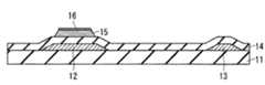
図1は、本発明の実施の一形態である薄膜トランジスタ1を備えるアクティブマトリックス基板10の構成を示す平面図である。図2は、図1の切断面線II−IIにおける断面構成を示す断面図である。本実施の形態では、薄膜トランジスタ(Thin Film Transistor;略称:TFT)1を備える薄膜トランジスタ基板として、スイッチング素子としてTFT1を備えるアクティブマトリックス基板10について説明する。本実施の形態のアクティブマトリックス基板10は、表示装置に使用される表示装置用TFTアクティブマトリックス基板である。 FIG. 1 is a plan view showing a configuration of an
アクティブマトリックス基板10は、ガラスなどの透明絶縁性基板11、ゲート電極12、ゲート配線12A、補助容量電極13、ゲート絶縁膜14、酸化物半導体膜15、酸化物導電膜16、ソース電極17、ソース配線17A、ドレイン電極18、保護絶縁膜20および画素電極22を備えて構成される。 The
ゲート配線12Aは、図1の紙面に向かって左右方向に延在し、ゲート電極12と接続される。ソース配線17Aは、図1の紙面に向かって上下方向に延在し、ソース電極17と接続される。ゲート配線12Aおよび補助容量電極13は、ゲート電極12と同時に形成される。ソース配線17Aは、ソース電極17と同時に形成される。 The
酸化物半導体膜15および酸化物導電膜16は、半導体層を構成する。換言すれば、半導体層は、酸化物半導体膜と酸化物導電膜との2層を含む。具体的には、酸化物半導体膜15は、ゲート絶縁膜14上に積層され、酸化物半導体で構成される。酸化物導電膜16は、酸化物半導体膜上に積層され、導電性酸化物で構成される。この酸化物半導体膜15と酸化物導電膜16とが積層された2層を含んで、半導体層が構成される。 The
ゲート電極12、ゲート絶縁膜14および半導体層は、この順に、透明絶縁性基板11上に積層される。本実施の形態では、半導体層は、酸化物半導体膜15と酸化物導電膜16との2層で構成される。 The
図2に示す断面構成において、ソース電極17およびドレイン電極18は、半導体層上で互いに離間して対向するように設けられる。対向するソース電極17とドレイン電極18との間の半導体層の領域、すなわちソース電極7のパターンとドレイン電極18のパターンとに挟まれた半導体層の領域は、TFT1のチャネル領域19となっている。チャネル領域19は、酸化物導電膜16が除去されて、酸化物半導体膜によって形成されており、バックチャネル領域となっている。 In the cross-sectional configuration shown in FIG. 2, the
ソース電極17およびドレイン電極18は、少なくとも、互いに対向する側の端部が、酸化物導電膜16を介して酸化物半導体膜15と電気的に接続されている。すなわち、ソース電極17およびドレイン電極18は、互いに対向する側の端部のみが、酸化物導電膜16を介して酸化物半導体膜15と電気的に接続されてもよいし、互いに対向する側の端部を含む一部分、またはソース電極17およびドレイン電極18の全体が、酸化物導電膜16を介して酸化物半導体膜15と電気的に接続されてもよい。 At least end portions of the
酸化物半導体膜15は、端面の断面形状、具体的にはソース電極17およびドレイン電極18で覆われる端面の断面形状が、略テーパー形状になっている。ここで、「略テーパー形状」とは、テーパー形状、およびテーパー形状に類似する形状を含む。テーパー形状に類似する形状としては、たとえば、後述する順階段形状がある。 In the
保護絶縁膜20は、チャネル領域19を保護して、透明絶縁性基板11全体に形成される。保護絶縁膜20には、下層のドレイン電極18の表面まで貫通した画素ドレインコンタクトホール21が形成されている。画素電極22は、透光性導電膜で構成され、画素ドレインコンタクトホール21を介して、下層のドレイン電極18に電気的に接続される。 The protective
本実施の形態のTFT1を備えるアクティブマトリックス基板10は、たとえば以下のようにして製造される。図3〜図7は、アクティブマトリックス基板10の製造工程を示す図である。 The
図3は、ゲート電極12および補助容量電極13の形成が終了した段階の状態を示す断面図である。まず、ガラス基板などの透明絶縁性基板11を洗浄液または純水を用いて洗浄し、ゲート電極12および補助容量電極13となる第1の金属膜を成膜する。第1の金属膜としては、たとえばクロム(Cr)、モリブデン(Mo)、チタン(Ti)、タンタル(Ta)、タングステン(W)、アルミニウム(Al)またはこれらに他の元素を微量に添加した合金などを用いる。またこれらの金属または合金を2層以上形成した積層構造としてもよい。これらの金属または合金を用いることによって、第1の金属膜として、比抵抗値が50μΩcm以下の低抵抗膜を得ることができる。 FIG. 3 is a cross-sectional view showing a state in which the formation of the
本実施の形態では、第1の金属膜としてMo膜を、たとえば、アルゴン(Ar)ガスを用いたスパッタリング法によって、たとえば200nmの厚さで成膜する。第1の金属膜の厚さは、これに限定されない。第1金属膜の厚さは、所望の配線抵抗が得られる値に設定すればよく、たとえば、第1金属膜として用いる金属膜の比抵抗値によって適正な値が決まる。 In the present embodiment, a Mo film is formed as the first metal film with a thickness of, for example, 200 nm by a sputtering method using, for example, argon (Ar) gas. The thickness of the first metal film is not limited to this. The thickness of the first metal film may be set to a value that provides a desired wiring resistance. For example, an appropriate value is determined by the specific resistance value of the metal film used as the first metal film.
第1金属膜の厚さは、膜質を維持するためには、5nm以上にすることが好ましく、生産性の低下および応力による膜剥がれを防止するためには、500nm以下にすることが好ましい。すなわち、第1金属膜の厚さは、5nm以上500nm以下であることが好ましい。 The thickness of the first metal film is preferably 5 nm or more in order to maintain the film quality, and is preferably 500 nm or less in order to prevent a decrease in productivity and film peeling due to stress. That is, the thickness of the first metal film is preferably 5 nm or more and 500 nm or less.
その後、第1回目の写真製版工程でフォトレジストパターンを形成する。形成したフォトレジストパターンをマスクとして、エッチング液を用いてウエットエッチングを行う。エッチング液としては、たとえば、リン酸(Phosphoric acid)、酢酸(Acetic acid)および硝酸(Nitric acid)を含む薬液であるPAN薬液を用いる。PAN薬液の液温は、たとえば40℃に設定する。 Thereafter, a photoresist pattern is formed in the first photolithography process. Wet etching is performed using an etching solution using the formed photoresist pattern as a mask. As the etching solution, for example, a PAN chemical solution that is a chemical solution containing phosphoric acid, acetic acid, and nitric acid is used. The liquid temperature of the PAN chemical solution is set to 40 ° C., for example.
ウエットエッチング後、フォトレジストパターンを除去する。以上のウエットエッチングプロセスによって、ゲート電極12および補助容量電極13を形成する。 After the wet etching, the photoresist pattern is removed. The
このウエットエッチングプロセスに用いるPAN薬液としては、リン酸が40wt%(重量%)以上93wt%以下であり、酢酸が1wt%以上40wt%以下であり、硝酸が0.5wt%以上15wt%以下である範囲のものが好ましい。本実施の形態では、たとえば、リン酸が70wt%であり、酢酸が7wt%であり、硝酸が5wt%であり、残部が水のPAN薬液を用いる。これによって、図3に示すように、Mo膜から成るゲート電極12および補助容量電極13のパターン側壁の断面形状を概略テーパー状に加工することができる。 As the PAN chemical used in this wet etching process, phosphoric acid is 40 wt% (wt%) or more and 93 wt% or less, acetic acid is 1 wt% or more and 40 wt% or less, and nitric acid is 0.5 wt% or more and 15 wt% or less. A range is preferred. In the present embodiment, for example, phosphoric acid is 70 wt%, acetic acid is 7 wt%, nitric acid is 5 wt%, and the balance is water PAN chemical. As a result, as shown in FIG. 3, the cross-sectional shapes of the pattern side walls of the
図4は、ゲート絶縁膜14、酸化物半導体膜15および酸化物導電膜16の形成が終了した段階の状態を示す断面図である。前述のようにしてゲート電極12および補助容量電極13を形成した後、ゲート絶縁膜14、酸化物半導体膜15および酸化物導電膜16を順次成膜して、TFT1の半導体パターンを形成する。以下に、図4に示すゲート絶縁膜14、酸化物半導体膜15および酸化物導電膜16を形成する工程を、図8〜図10を用いて具体的に説明する。 FIG. 4 is a cross-sectional view illustrating a state where the formation of the
図8は、フォトレジストパターン23の形成が終了した段階の状態を示す断面図である。前述のようにして図3に示すゲート電極12および補助容量電極13の形成が終了した後、ゲート電極12および補助容量電極13が形成された透明絶縁性基板(以下、単に「基板」という場合がある)11上に、まず、全面にわたって、ゲート絶縁膜14を形成する。 FIG. 8 is a cross-sectional view showing a state where the formation of the
本実施の形態では、たとえば、化学気相成長(Chemical Vapor Deposition;略称:CVD)法を用いて、約300℃の基板加熱条件下で、ゲート絶縁膜14として酸化シリコン(SiO)膜を300nmの厚さで成膜する。ゲート絶縁膜14の成膜方法、基板11の加熱温度およびゲート絶縁膜14の厚さは、これに限定されない。 In this embodiment, for example, a silicon oxide (SiO) film having a thickness of 300 nm is used as the
ゲート絶縁膜14の厚さは、TFT1の動作をさせるための所望の電界強度が得られる値に設定すればよく、たとえば、ゲート絶縁膜14として用いる絶縁膜の誘電率値によって適正な値が決まる。ゲート絶縁膜14の厚さは、膜質を維持するためには、5nm以上にすることが好ましく、応力による膜剥がれを防止するためには、3000nm以下にすることが好ましい。すなわち、ゲート絶縁膜14の厚さは、5nm以上3000nm以下であることが好ましい。また、ゲート絶縁膜14として、塗布によって形成された絶縁膜を用いる場合には、ゲート絶縁膜14の厚さは、1000nm以上3000nm以下であることが好ましい。 The thickness of the
酸化シリコン膜は、水分(H2O)および水素(H2)、ならびにナトリウム(Na)およびカリウム(K)などのTFT特性に影響を及ぼす不純物元素に対するバリア性、すなわち遮断性が弱い。したがって、ゲート絶縁膜14として酸化シリコン膜を用いる場合には、酸化シリコン膜の下層に、バリア性に優れる膜、たとえば窒化シリコン(SiN)膜などを設けて、ゲート絶縁膜14を積層構造としてもよい。The silicon oxide film has a weak barrier property, that is, a blocking property against impurity elements that affect TFT characteristics such as moisture (H2 O) and hydrogen (H2 ), and sodium (Na) and potassium (K). Therefore, when a silicon oxide film is used as the
次に、酸化物半導体膜15を下層、酸化物導電膜16を上層とする積層構造を、たとえばスパッタリング法で成膜する。ここで、酸化物半導体とは、原則としてn型の導電型を有し、導電率が1×10⁻⁷S/cm以上10S/cm以下であるもの、または、キャリアとなる電子の濃度(以下「キャリア濃度」という場合がある)が1×1011個/cm3以上1018個/cm3以下であるものとする。Next, a stacked structure in which the
導電率が10S/cmよりも大きい場合、およびキャリア濃度が1×1018個/cm3よりも大きい場合は、電流が常時流れやすくなり、TFTがオフ状態でも、オフ電流と呼ばれる電流が流れ、半導体膜としてのスイッチングの機能を示さない場合がある。したがって、導電率は10S/cm以下であることが好ましく、キャリア濃度は1018個/cm3以下であることが好ましい。When the conductivity is higher than 10 S / cm, and when the carrier concentration is higher than 1 × 10¹⁸ cells / cm3 , the current always flows easily, and even when the TFT is in the off state, a current called an off current flows. In some cases, the switching function as a semiconductor film is not exhibited. Therefore, the electrical conductivity is preferably 10 S / cm or less, and the carrier concentration is preferably 1018 / cm3 or less.
また、導電率が1×10⁻⁷S/cmよりも小さい場合、およびキャリア濃度が1×1011個/cm3よりも小さい場合は、TFTがオン状態でもオン電流がほとんど流れず、スイッチングの機能を示さない場合がある。したがって、導電率は1×10−7S/cm以上であることが好ましく、キャリア濃度は1×1011個/cm3以上であることが好ましい。In addition, when the conductivity is lower than 1 × 10⁻⁷ S / cm and when the carrier concentration is lower than 1 × 10¹¹ cells / cm3 , the on-state current hardly flows even when the TFT is in an on state. May not show function. Therefore, the conductivity is preferably 1 × 10⁻⁷ S / cm or more, and the carrier concentration is preferably 1 × 10¹¹ pieces / cm3 or more.
以上のことから、前述のように酸化物半導体は、導電率が1×10⁻⁷S/cm以上10S/cm以下であるか、または、キャリア濃度が1×1011個/cm3以上1018個/cm3以下であることが好ましい。酸化物半導体は、導電率が1×10−5S/cm以上1×10−1S/cm以下であるか、またはキャリア濃度が1×1012個/cm3以上1×1017個/cm3以下であることが、さらに好ましい。From the above, the oxide semiconductor has a conductivity of 1 × 10⁻⁷ S / cm to 10 S / cm or a carrier concentration of 1 × 10¹¹ pieces /
このような酸化物半導体で構成される酸化物半導体膜15でチャネル領域19を形成することによって、アモルファスシリコンよりも高い移動度を有するTFT1を実現することができる。これに対して、上層の酸化物導電膜16は、導電率が1×10S/cm以上、より好ましくは1×102S/cm以上のいわゆる導電性の膜とする。By forming the
本実施の形態では、下層の酸化物半導体膜15の材料として、酸化亜鉛(ZnO)に酸化インジウム(In2O3)、および酸化錫(SnO2)を添加したIn―Zn−Sn−O系の酸化物を用いる。具体的には、In、Zn、Sn、Oの原子組成比が2:6:2:13であるIn−Zn−Sn−Oターゲット[In2O3・(ZnO)6・(SnO2)2]を用いて、Arガスに対して分圧比で10%の酸素(O2)ガスを添加した混合ガスによるスパッタリングを行い、40nmの厚さで酸化物半導体膜15を成膜する。酸化物半導体膜15の材料、成膜方法および厚さは、これに限定されない。酸化物半導体膜15の厚さは、膜質を維持するためには、5nm以上であることが好ましい。In this embodiment, the material of the lower
その後、上層の酸化物導電膜16として、酸化亜鉛(ZnO)に酸化インジウム(In2O3)を添加したIn−Zn−O系の酸化物導電膜を成膜する。具体的には、In2O3が90重量%、ZnOが10重量%の配合比であるIn−Zn−Oターゲットを用いて、Arガスによるスパッタリングを行い、20nmの厚さで酸化物導電膜16を成膜する。After that, an In—Zn—O-based oxide conductive film obtained by adding indium oxide (In2 O3 ) to zinc oxide (ZnO) is formed as the upper oxide
酸化物導電膜16の材料、成膜方法および厚さは、これに限定されない。酸化物導電膜16の厚さは、良好なテーパー形状を形成する観点からは、酸化物半導体膜15の厚さよりも小さくすることが好ましく、酸化物半導体膜15の厚さの半分以下とすることがさらに好ましい。 The material, the deposition method, and the thickness of the oxide
以上の条件で成膜したIn−Zn−Sn−O系酸化物半導体膜15は、たとえば、導電率が1.5×10⁻⁵S/cmであり、キャリア濃度が1.1×1014個/cm3である。また、In−Zn−O系酸化物導電膜16は、たとえば、導電率が1.8×103S/cmであり、キャリア濃度が7.4×1020個/cm3である。The In—Zn—Sn—O-based
酸化物半導体膜15および酸化物導電膜16は、いずれも酸化物系の膜であるので、両者を積層した場合でも、界面の還元反応が生じることがない。したがって、ダメージ層が形成されることはない。 Since both the
次に、第2回目の写真製版工程でフォトレジストパターン23を形成する。本実施の形態では、まず、ノボラック樹脂系のポジ型フォトレジストを、スリットコータまたはスピンコータによって、たとえば約1.6μmの厚さで塗布した後に、フォトマスクを用いて露光を行う。その後、水酸化テトラメチルアンモニウム(Tetramethylammonium hydroxide;略称:TMAH)を含む有機アルカリ系の現像液を用いて現像を行い、フォトレジストパターン23を形成する。フォトレジストパターン23の材料、形成方法、厚さおよび現像液は、これに限定されない。 Next, a
図9は、酸化物半導体膜15および酸化物導電膜16のエッチングが終了した段階の状態を示す断面図である。前述のようにしてフォトレジストパターン23を形成した後、形成したフォトレジストパターン23をマスクとして、エッチング液として、たとえばシュウ酸溶液を用いて、フォトレジストパターン23で覆われていない部分の酸化物導電膜16および酸化物半導体膜15をエッチングによって除去する。 FIG. 9 is a cross-sectional view illustrating a state where the etching of the
図10は、フォトレジストパターン23の除去が終了した段階の状態を示す断面図である。前述のようにして酸化物導電膜16および酸化物半導体膜15のエッチングが終了した後、フォトレジストパターン23を、たとえば剥離剤によって剥離させて除去する。これによって、図10に示すテーパー形状の酸化物導電膜16および酸化物半導体膜15が形成される。 FIG. 10 is a cross-sectional view showing a state where the removal of the
図8〜図10に示すゲート絶縁膜14、酸化物半導体膜15および酸化物導電膜16を形成する工程を、図11〜図15を用いて、以下に、さらに具体的に説明する。図11〜図15では、理解を容易にするために、ゲート絶縁膜14、酸化物半導体膜15、酸化物導電膜16およびフォトレジストパターン23の部分のみを記載する。 The process of forming the
図11は、酸化物導電膜16の形成が終了した段階の状態を示す断面図である。図11に示す状態は、前述の図8に示すゲート絶縁膜14、酸化物半導体膜15、酸化物導電膜16およびフォトレジストパターン23を形成する工程において、酸化物導電膜16の形成が終了した段階の状態に相当する。図11に示すように、前述のようにしてゲート絶縁膜14、酸化物半導体膜15および酸化物導電膜16を形成する。 FIG. 11 is a cross-sectional view showing a state where the formation of the oxide
図12は、フォトレジストパターン23の形成が終了した段階の状態を示す断面図である。図12に示す状態は、前述の図8に示すゲート絶縁膜14、酸化物半導体膜15、酸化物導電膜16およびフォトレジストパターン23を形成する工程において、フォトレジストパターン23の形成が終了した段階の状態に相当する。前述のようにして形成された酸化物導電膜16上に、図12に示すように、フォトレジストパターン23を形成する。 FIG. 12 is a cross-sectional view showing a state where the formation of the
図13は、酸化物半導体膜15および酸化物導電膜16のエッチングの途中段階の状態を示す断面図である。図14は、酸化物半導体膜15および酸化物導電膜16のエッチングが終了した段階の状態を示す断面図である。図15は、フォトレジストパターン23の除去が終了した段階の状態を示す断面図である。 FIG. 13 is a cross-sectional view illustrating a state in the middle of etching of the
前述のようにしてフォトレジストパターン23を形成した後、たとえば、エッチング液としてシュウ酸溶液を用いて、液温45℃の条件で、酸化物導電膜であるIn−Zn−O系酸化物導電膜16とIn−Zn−Sn−O系の酸化物半導体膜15の同時エッチングを行う。 After the
このとき、酸化物半導体膜15の単層膜におけるエッチング速度(エッチングレート)は、たとえば92nm/分であり、酸化物導電膜6の単層膜におけるエッチング速度は、たとえば220nm/分である。この場合、酸化物半導体膜15のエッチング速度は、酸化物導電膜16のエッチング速度の2分の1(1/2)以下である。酸化物半導体膜15および酸化物導電膜16のエッチング速度は、これに限定されない。 At this time, the etching rate (etching rate) in the single layer film of the
薬液を用いたウエットエッチング法の場合、エッチングは、等方的に進行するので、酸化物導電膜16であるIn−Zn−O膜は、横方向、すなわち膜の面内方向にも酸化物半導体膜15よりも速くエッチングが進行する。エッチングの初期から中間段階では、図13に示すように、酸化物導電膜16の幅が、フォトレジストパターン23の幅よりも狭くなる。つまり、酸化物導電膜16の端面がフォトレジストパターン23の端面よりも後退する。これに対し、酸化物半導体膜15は、酸化物導電膜16よりもエッチングの進行が遅い。したがって、酸化物導電膜16が後退したことによるアンダーカット状のノッチ24が形成される。 In the case of a wet etching method using a chemical solution, etching proceeds isotropically. Therefore, the In—Zn—O film that is the oxide
このようなノッチ24が形成されると、このノッチ24の部分に薬液が浸み込みやすくなり、他の部分よりもエッチングが加速される。この状態で、上層の酸化物導電膜16と下層の酸化物半導体膜15とが同時にエッチングされることによって、図14に示すように、酸化物導電膜16と酸化物半導体膜15との積層構造に、テーパー形状が形成される。 When such a
このようにしてテーパー形状を形成した後、残存するフォトレジストパターン23を前述のようにして除去することによって、図15に示すテーパー形状の酸化物導電膜16および酸化物半導体膜15が得られる。 After forming the tapered shape in this way, the remaining
以上のようなエッチングの進行を実現するために、エッチング条件は、酸化物導電膜16のエッチング速度が、酸化物半導体膜15のエッチング速度よりも高くなるような条件とすることが好ましい。これに加えて、酸化物半導体膜15の膜厚t1と酸化物導電膜16の膜厚t2との関係を、「酸化物半導体膜15の膜厚t1が、酸化物導電膜16の膜厚t2よりも大きい(t1>t2)」とすることがより好ましい。 In order to realize the progress of the etching as described above, the etching conditions are preferably set such that the etching rate of the oxide
酸化物半導体膜15の膜厚t1と酸化物導電膜16の膜厚t2とを等しくした場合は、上層の酸化物導電膜16と下層の酸化物半導体膜15とがそれぞれ独立した階段形状になる。このような場合でも、「酸化物導電膜16のエッチング速度V2が、酸化物半導体膜16のエッチング速度V1よりも高い(V2>V2)」となる条件であれば、上層の酸化物導電膜16の端面が下層の酸化物半導体膜15の端面よりも後退して順階段形状となる。これによって、この後に形成される保護絶縁膜10のカバレッジを改善することができるので好ましい。 When the film thickness t1 of the
酸化物半導体膜15の膜厚t1は、酸化物導電膜16の膜厚t2の2倍以上(t1≧2(t2))とすることが好ましい。このように酸化物半導体膜15の膜厚t1を、酸化物導電膜16の膜厚t2の2倍以上(t1≧2(t2))とすることによって、酸化物半導体膜15および酸化物導電膜16の端面を順階段状ではなく、図15に示す本実施の形態のようにテーパー形状にすることができる。テーパー形状にすることによって、順階段形状の場合に比べて、保護絶縁膜20のカバレッジ性を向上させることができるので好ましい。 The film thickness t1 of the
以上のようにして図9に示す酸化物半導体膜15および酸化物導電膜16のエッチングを行った後、フォトレジストパターン23を、たとえばアミン系の剥離液を用いて剥離することによって除去する。これによって、図10に示す酸化物半導体膜15と酸化物導電膜16との半導体パターンを形成する。図10に示す状態は、図15に示す状態に相当する。 After the
以上のようにして図4に示すテーパー形状の酸化物半導体膜15および酸化物導電膜16を形成した後、図5に示すソース電極17およびドレイン電極18を形成する工程に移行する。図5は、ソース電極17およびドレイン電極18の形成が終了した段階の状態を示す図である。 After the tapered
酸化物半導体膜15および酸化物導電膜16のエッチング後、テーパー形状の酸化物半導体膜15および酸化物導電膜16が形成された透明絶縁性基板11上に、ソース電極17およびドレイン電極18となる第2の金属膜を成膜する。成膜した第2の金属膜をパターニングして、ソース電極17およびドレイン電極18を、互いに対向するように形成する。さらに、互いに対向するソース電極17のパターンとドレイン電極18のパターンとに挟まれた領域の酸化物導電膜16を除去して、TFT1のバックチャネル領域であるチャネル領域19を形成する。 After the
第2の金属膜としては、たとえばアルミニウム(Al)、チタン(Ti)、クロム(Cr)、銅(Cu)、モリブデン(Mo)、タンタル(Ta)もしくはタングステン(W)、またはこれらに他の元素を微量に添加した合金などを用いることができる。また、第2の金属膜は、これらの金属および合金のいずれかで構成される金属膜を2層以上形成した積層構造としてもよい。これらの金属および合金のいずれかを用いることによって、第2の金属膜として、比抵抗値が50μΩcm以下の低抵抗膜を得ることができる。 Examples of the second metal film include aluminum (Al), titanium (Ti), chromium (Cr), copper (Cu), molybdenum (Mo), tantalum (Ta), tungsten (W), and other elements. An alloy to which a small amount of is added can be used. The second metal film may have a laminated structure in which two or more metal films made of any of these metals and alloys are formed. By using any of these metals and alloys, a low resistance film having a specific resistance value of 50 μΩcm or less can be obtained as the second metal film.
本実施の形態では、第2の金属膜としてMo膜を、たとえば、公知のArガスを用いたスパッタリング法で、200nmの厚さで成膜する。その後、図示は省略するが、第3回目の写真製版工程でフォトレジストパターンを形成し、形成したフォトレジストパターンをマスクとして、前述の図3に示すゲート電極12および補助容量電極13を形成したときと同じエッチング液、具体的にはリン酸、硝酸および酢酸を含むPAN薬液を用いて、第2の金属膜であるMo膜、および酸化物導電膜16を、連続でウエットエッチングする。 In this embodiment, a Mo film is formed as the second metal film with a thickness of 200 nm by a sputtering method using a known Ar gas, for example. Thereafter, although not shown, when a photoresist pattern is formed in the third photolithography process, and the
このとき、TFT1のチャネル領域19においては、PAN薬液で第2の導電膜がエッチング除去された後に表面が露出したIn−Zn−O系の酸化物導電膜16が、さらにPAN薬液中でエッチング除去される。またIn−Zn−O系の酸化物導電膜16がエッチング除去された後に表面が露出するIn−Zn−Sn−O系の酸化物半導体膜15は、PAN薬液にほとんど溶けないのでエッチングされずに残り、チャネル領域19となる。 At this time, in the
その後、フォトレジストパターンを除去することによって、図5に示すソース電極17、ドレイン電極18、およびTFT1のチャネル領域19が得られる。 Thereafter, by removing the photoresist pattern, the
本実施の形態のように第2の金属膜としてMo膜を用いた場合、Mo膜の横方向のエッチング量が、In−Zn−O系の酸化物導電膜16に比べて大きい、換言すれば、Mo膜の横方向のエッチング速度が、In−Zn−O系の酸化物導電膜16に比べて高いので、酸化物導電膜16とソース電極17およびドレイン電極18のチャネル領域19側の端面とが段差形状となる。 When a Mo film is used as the second metal film as in this embodiment, the lateral etching amount of the Mo film is larger than that of the In—Zn—O-based oxide
これによって、後述する保護絶縁膜20のカバレッジ性を向上させることができる。したがって、ソース電極17およびドレイン電極17の端部へのボイドの発生を抑制することができるので、TFT特性に影響を与える水分などの影響を除外することができ、高品質のTFT1およびそれを備えるデイバスを高歩留で製造することができる。 Thereby, the coverage of the protective insulating
チャネル領域19の酸化物導電膜16を除去した後には、酸化物半導体膜15のチャネル領域19の表面を、さらにTMAHを含むアルカリ溶液で洗浄してもよいし、またはプラズマを照射する処理(以下「プラズマ処理」という場合がある)を行ってもよい。 After the oxide
プラズマ処理は、ヘリウム(He)、ネオン(Ne)、アルゴン(Ar)、窒素(N2)、または六フッ化硫黄(SF6)、四フッ化炭素(CF4)、フッ素(F2)、フッ化水素(HF)、三フッ化窒素(NF3)、三フッ化メタン(CHF3)もしくは六フッ化エタン(C2F6)などのフッ素を含むガスなどのプラズマを用いて行うことができる。Plasma treatment is performed using helium (He), neon (Ne), argon (Ar), nitrogen (N2 ), sulfur hexafluoride (SF6 ), carbon tetrafluoride (CF4 ), fluorine (F2 ), It is performed using plasma such as a gas containing fluorine such as hydrogen fluoride (HF), nitrogen trifluoride (NF3 ), trifluoromethane (CHF3 ), or hexafluoroethane (C2 F6 ). it can.
これらのガスを用いてプラズマ処理を行うことによって、チャネル領域19の表面の異物および汚染物を除去して、TFT1のオフ特性を良好にする、具体的にはオフ電流を低減することができる。 By performing plasma treatment using these gases, foreign matters and contaminants on the surface of the
また、酸素(O2)ガスまたは一酸化二窒素(N2O)ガスを用いてプラズマ処理を行ってもよい。この場合は、チャネル領域19の表面の異物および汚染物を除去するとともに、酸化物半導体膜15のチャネル領域19の表面に酸素原子を供給することによって表面近傍を高抵抗化させ、TFT1のオフ特性をさらに良好にすることができる。Alternatively, plasma treatment may be performed using oxygen (O2 ) gas or dinitrogen monoxide (N2 O) gas. In this case, foreign matter and contaminants on the surface of the
図6は、保護絶縁膜20の形成が終了した段階の状態を示す断面図である。前述のようにしてソース電極17およびドレイン電極18を形成した後に、保護絶縁膜20を成膜する。本実施の形態では、保護絶縁膜20として、たとえば、CVD法を用いて、約250℃の基板加熱条件下で酸化シリコンSiO膜を300nmの厚さで成膜する。保護絶縁膜20の材料、成膜方法、基板加熱温度および厚さは、これに限定されない。 FIG. 6 is a cross-sectional view showing a state where the formation of the protective insulating
その後、第4回目の写真製版工程でフォトレジストパターンを形成して、公知のフッ素系ガスを用いたドライエッチング法を用いてSiO膜をエッチングした後に、フォトレジストパターンを除去して、画素ドレインコンタクトホール21を形成する。 Thereafter, a photoresist pattern is formed in the fourth photoengraving process, and after etching the SiO film by using a dry etching method using a known fluorine-based gas, the photoresist pattern is removed to obtain a pixel drain contact.
酸化シリコン膜は、水分(H2O)および水素(H2)、ならびにナトリウム(Na)およびカリウム(K)などのアルカリ金属のようなTFT特性に影響を及ぼす不純物元素に対するバリア性(遮断性)が弱いので、酸化シリコン膜の上層に、たとえばバリア性に優れる窒化シリコン(SiN)膜などを設けて、保護絶縁膜20を積層構造としてもよい。このような積層構造の場合でも、公知のフッ素ガスを用いたドライエッチング法を用いて、画素ドレインコンタクトホール21を形成することができる。The silicon oxide film has a barrier property (blocking property) against impurity elements that affect TFT characteristics such as moisture (H2 O) and hydrogen (H2 ), and alkali metals such as sodium (Na) and potassium (K). Therefore, for example, a silicon nitride (SiN) film having excellent barrier properties may be provided on the silicon oxide film, and the protective insulating
図7は、透明画素電極22の形成が終了した段階の状態を示す断面図である。前述のようにして画素ドレインコンタクトホール21を形成した後、全面にわたって、透明画素電極22となる透明導電性膜を成膜する。成膜した透明導電性膜をパターニングし、画像表示用の透明画素電極22を形成する。 FIG. 7 is a cross-sectional view showing a state in which the formation of the
本実施の形態では、透明導電性膜として、たとえば、前述の酸化物導電膜16と同じ材料であるIn−Zn−O膜を、公知のArガスを用いたスパッタリング法で、100nmの厚さで成膜する。透明導電成膜の材料、成膜方法および厚さは、これに限定されない。 In this embodiment, for example, an In—Zn—O film that is the same material as the above-described oxide
次いで、第5回目の写真製版工程でフォトレジストパターンを形成し、形成したフォトレジストパターンをマスクとして、たとえば公知のシュウ酸系溶液でウエットエッチングする。その後、フォトレジストパターンを除去して、透明画素電極22を形成する。以上のようにして、図1に示す本実施の形態における液晶ディスプレイ用のTFTアクティブマトリックス基板10を製造する。 Next, a photoresist pattern is formed in the fifth photolithography process, and wet etching is performed with, for example, a known oxalic acid-based solution using the formed photoresist pattern as a mask. Thereafter, the photoresist pattern is removed, and the
以上の5回の写真製版工程によって製造されたTFTアクティブマトリックス基板10を用いて液晶表示装置を製造する場合、図示は省略するが、製造されたTFTアクティブマトリックス基板10の表面に、液晶を配列させるためのポリイミドなどからなる配向膜、およびスペーサーを形成する。 When a liquid crystal display device is manufactured using the TFT
その後、TFTアクティブマトリックス基板10と、カラーフィルタおよび配向膜を備える対向基板とを貼り合わせ、前述のスペーサーによって両基板の間に形成される隙間に液晶を注入して保持する。さらに両基板の外側に偏光板、位相差板およびバックライトユニットなどを配設することによって、液晶表示装置を得ることができる。 Thereafter, the TFT
以上のように本実施の形態によれば、酸化物半導体膜15と酸化物導電膜16とが積層された2層を含む半導体層が形成される。酸化物導電膜16は、エッチング液によってエッチングされるときのエッチング速度が、酸化物半導体膜のエッチング速度よりも高くなるように形成される。具体的には、酸化物導電膜16は、燐酸、硝酸および酢酸を含むPAN薬液によってエッチングされるときのエッチング速度が、酸化物半導体膜15のエッチング速度よりも高い材料で構成される。これによって、酸化物半導体膜15および酸化物導電膜16を含む半導体層を、容易に、端面の断面形状が略テーパー形状にすることができる。 As described above, according to this embodiment, a semiconductor layer including two layers in which the
具体的には、エッチング液として、シュウ酸を含む薬液、または燐酸、硝酸および酢酸を含むPAN薬液を用いて、半導体層をウエットエッチングすることによって、酸化物半導体膜15および酸化物導電膜16を含み、端面の断面形状が略テーパー形状の半導体層を、容易に形成することができる。 Specifically, the
このように、酸化物半導体膜15および酸化物導電膜16を含む半導体層を、端面の断面形状が略テーパー形状にすることによって、酸化物半導体膜15の上層にあるソース電極17およびドレイン電極18の断線を抑制することができる。 In this manner, the semiconductor layer including the
また、酸化物導電膜16を設けることによって、ソース電極17およびドレイン電極18とチャネル層である半導体層との接合端部において、ソース電極17およびドレイン電極18との接続界面部を有する第2の半導体材料である酸化物導電膜16の端部が、ソース電極17およびドレイン電極18の端部よりも内側に後退された構成となるので、電極端部における電界集中を抑制して、良好なTFT特性を得ることができる。 Further, by providing the oxide
また、ソース電極17およびドレイン電極18は、少なくとも、互いに対向する側の端部が、それぞれ酸化物導電膜16を介して酸化物半導体膜15と電気的に接続された構成となっているので、ソース電極17およびドレイン電極18と酸化物半導体膜15の活性層との接続界面における電気特性を向上させることができる。これによって、酸化物半導体膜15の比較的高いキャリア移動度を活かして、動作速度が比較的速い高性能のTFTアクティブマトリックス基板10およびそれを備える表示装置を、高い歩留で生産性よく製造することができる。 In addition, the
本実施の形態では、酸化物半導体膜15の材料としてIn−Zn−Sn−O系の酸化物を用い、酸化物導電膜16の材料としてIn−Zn−O系の酸化物を用い、エッチング薬液としてシュウ酸系薬液を用いたが、これらに限定されるものではない。ウエットエッチングのエッチング速度として、酸化物導電膜16のエッチング速度V2が酸化物半導体膜15のエッチング速度V1よりも高い(V2>V1)となるような酸化物およびエッチング薬液であれば、好適に用いることができる。 In this embodiment, an In—Zn—Sn—O-based oxide is used as the material of the
酸化物系の導電膜および半導体膜のエッチング薬液として、よく用いられるシュウ酸系薬液を選択した場合は、酸化物半導体膜15として、In−Zn−Sn−O系の他にも、たとえば、Zn−Sn−O系、In−Al−Sn−O系、In−Si−Sn−O系、In−Al−Zn−Sn−O系のような錫(Sn)を含む酸化物半導体膜を選択することができる。すなわち、酸化物半導体膜15は、酸化錫を含んでもよい。 When a frequently used oxalic acid-based chemical solution is selected as the etching chemical solution for the oxide-based conductive film and the semiconductor film, in addition to the In—Zn—Sn—O system, for example, Zn An oxide semiconductor film containing tin (Sn), such as a —Sn—O, In—Al—Sn—O, In—Si—Sn—O, or In—Al—Zn—Sn—O system, is selected. be able to. That is, the
酸化錫を含む酸化物半導体膜を用いることによって、酸化錫を含まない酸化物半導体膜を用いる場合に比べて、シュウ酸系またはカルボン酸系の薬液に対する酸化物半導体膜13のエッチング速度を低下させることができる。 By using an oxide semiconductor film containing tin oxide, the etching rate of the
酸化物導電膜16としては、In−Zn−O系の他にも,Zn−O系、ガリウム(Ga)−Zn−O系、Al−Zn−O系のようなZn−Oを含む酸化物導電膜を選択することができる。すなわち、酸化物導電膜16は、酸化亜鉛(ZnO)を含んでもよい。酸化亜鉛(ZnO)を含む酸化物導電膜16を用いることによって、シュウ酸薬液に対するエッチング速度が、酸化物導電膜16のエッチング速度V2が酸化物半導体膜15のエッチング速度V1よりも大きい(V2>V1)という条件を満足する酸化物導電膜16を容易に実現することができる。 As the oxide
酸化物半導体膜15を成膜した後には、200℃以上450℃以下の熱処理を行ってもよい。この熱処理の温度は、さらに好ましくは300℃以上400℃以下である。熱処理を行うことによって、シュウ酸系薬液に対する酸化物半導体膜15のエッチング速度をさらに低下させることができる。 After the
以上に述べた酸化物半導体膜15および酸化物導電膜16の各材料の元素の組成比は、導電率およびキャリア濃度がそれぞれ所望の値となるように決めればよい。 The elemental composition ratios of the materials of the
また、前述の酸化物半導体膜15と酸化物導電膜16との組み合わせに対して、エッチング薬液として、金属膜のエッチング薬液である前述のPAN薬液を用いることも可能である。 In addition, for the combination of the
この場合は、PAN薬液に対するエッチング速度が、ソース電極17およびドレイン電極18のエッチング速度V3、酸化物導電膜16のエッチング速度V2、酸化物半導体膜15のエッチング速度V1の順に小さくなる(V3>V2>V1)ようにそれぞれの材料を決めてやればよい。 In this case, the etching rate for the PAN chemical solution decreases in the order of the etching rate V3 of the
このような条件を満たすソース電極17およびドレイン電極18を構成する金属膜として、MoもしくはCuの膜、またはこれらの合金膜を好適に用いることができる。 As the metal film constituting the
すなわち、ソース電極17およびドレイン電極18は、PAN薬液によってエッチングすることが可能な金属材料で構成されてもよく、この場合の金属材料は、アルミニウム(Al)、モリブデン(Mo)および銅(Cu)、ならびにこれらの合金から選ばれる少なくとも1つを含む。 That is, the
このような材料でソース電極17およびドレイン電極18を構成することによって、ソース電極17およびドレイン電極18と、酸化物半導体膜15および酸化物導電膜16とを同時にエッチングすることができる。したがって、写真製版工程の数を削減することができるので、製造工程を簡略化することができる。 By forming the
なお、本発明は、その発明の範囲内において、各実施の形態を自由に組み合わせることが可能である。また、各実施の形態の任意の構成要素を適宜、変更または省略することが可能である。 The present invention can be freely combined with each embodiment within the scope of the invention. In addition, any component in each embodiment can be changed or omitted as appropriate.
1 薄膜トランジスタ(TFT)、10 アクティブマトリックス基板、11 透明絶縁性基板、12 ゲート電極、12A ゲート配線、13 補助容量電極、14 ゲート絶縁膜、15 酸化物半導体膜、16 酸化物導電膜、17 ソース電極、17A ソース配線、18 ドレイン電極、19 チャネル領域、20 保護絶縁膜、21 画素ドレインコンタクトホール、22 画素電極、23 フォトレジストパターン、24 ノッチ。 DESCRIPTION OF SYMBOLS 1 Thin film transistor (TFT), 10 Active matrix substrate, 11 Transparent insulating substrate, 12 Gate electrode, 12A Gate wiring, 13 Auxiliary capacity electrode, 14 Gate insulating film, 15 Oxide semiconductor film, 16 Oxide conductive film, 17 Source electrode , 17A source wiring, 18 drain electrode, 19 channel region, 20 protective insulating film, 21 pixel drain contact hole, 22 pixel electrode, 23 photoresist pattern, 24 notch.
Claims (14)
Translated fromJapanese前記半導体層上で互いに離間して対向するように設けられるソース電極およびドレイン電極とを備え、
前記半導体層は、
前記ゲート絶縁膜上に積層され、酸化物半導体で構成される酸化物半導体膜と、
前記酸化物半導体膜上に積層され、導電性酸化物で構成される酸化物導電膜との2層を含み、
前記酸化物半導体膜および前記酸化物導電膜の各々が酸化亜鉛を含み、
前記酸化物半導体膜および前記酸化物導電膜のうち前記酸化物半導体膜のみが酸化錫を含み、
前記ソース電極および前記ドレイン電極は、少なくとも、互いに対向する側の端部が、前記酸化物導電膜を介して前記酸化物半導体膜と電気的に接続され、
対向する前記ソース電極と前記ドレイン電極との間の前記半導体層には、前記酸化物半導体膜によってチャネル領域が形成されており、
前記チャネル領域上には前記酸化物導電膜が設けられておらず、前記ソース電極および前記ドレイン電極の間において前記酸化物導電膜は分離され、
前記酸化物半導体膜は、端面の断面形状が略テーパー形状であることを特徴とする薄膜トランジスタ。A gate electrode, a gate insulating film, and a semiconductor layer sequentially stacked on the substrate;
A source electrode and a drain electrode provided on the semiconductor layer so as to face each other at a distance from each other;
The semiconductor layer is
An oxide semiconductor film stacked on the gate insulating film and formed of an oxide semiconductor; and
Including two layers of an oxide conductive film stacked on the oxide semiconductor film and composed of a conductive oxide;
Each of the oxide semiconductor film and the oxide conductive film contains zinc oxide,
Of the oxide semiconductor film and the oxide conductive film, only the oxide semiconductor film contains tin oxide,
The source electrode and the drain electrode have at least ends facing each other electrically connected to the oxide semiconductor film through the oxide conductive film,
In the semiconductor layer between the source electrode and the drain electrode facing each other, a channel region is formed by the oxide semiconductor film,
The oxide conductive film is not provided on the channel region, and the oxide conductive film is separated between the source electrode and the drain electrode,
A thin film transistor, wherein the oxide semiconductor film has a substantially tapered cross-sectional shape at an end face.
前記スイッチング素子は、請求項1から6のいずれか1つに記載の薄膜トランジスタであることを特徴とするアクティブマトリックス基板。An active matrix substrate comprising a pixel electrode and a plurality of switching elements connected to the pixel electrode,
The switching device, an active matrix substrate which is a thin film transistor according to any one of claims 1 to6.
基板上に、ゲート電極およびゲート絶縁膜を順に形成する工程と、
前記ゲート絶縁膜上に、酸化物半導体で構成される酸化物半導体膜を形成する工程と、
前記酸化物半導体膜上に、導電性酸化物で構成される酸化物導電膜を形成して、前記酸化物半導体膜と前記酸化物導電膜とが積層された2層を含む半導体層を形成する工程と、
を備え、前記酸化物半導体膜および前記酸化物導電膜のうち前記酸化物半導体膜のみが酸化錫を含み、さらに、
前記半導体層をウエットエッチングする工程と、
前記半導体層上に金属膜を形成する工程と、
ウエットエッチングによって、前記金属膜からソース電極およびドレイン電極を形成し、かつ前記ソース電極と前記ドレイン電極との間で前記酸化物導電膜を除去することにより、当該酸化物導電膜を前記ソース電極と前記ドレイン電極との間で分離する工程と、を備えることを特徴とする薄膜トランジスタの製造方法。A method of manufacturing a thin film transistor, comprising: a gate electrode, a gate insulating film, and a semiconductor layer that are sequentially stacked on a substrate; and a source electrode and a drain electrode that are provided on the semiconductor layer so as to be spaced apart from each other,
Forming a gate electrode and a gate insulating film in order on the substrate;
Forming an oxide semiconductor film made of an oxide semiconductor on the gate insulating film;
An oxide conductive film formed using a conductive oxide is formed over the oxide semiconductor film, and a semiconductor layer including two layers in which the oxide semiconductor film and the oxide conductive film are stacked is formed. Process,
Of the oxide semiconductor film and the oxide conductive film, only the oxide semiconductor film contains tin oxide,
Wet etching the semiconductor layer;
Forming a metal film on the semiconductor layer;
By forming a source electrode and a drain electrode from the metal film by wet etching, and removing the oxide conductive film between the source electrode and the drain electrode, theoxide conductive film and the source electrode are removed.And a stepof separating the drain electrode from the drain electrode .
シュウ酸を含む薬液によって、前記半導体層をウエットエッチングすることを特徴とする請求項8に記載の薄膜トランジスタの製造方法。In the step of wet etching the semiconductor layer,
9. The method of manufacturing a thin film transistor according to claim8 , wherein the semiconductor layer is wet-etched with a chemical solution containing oxalic acid.
燐酸、硝酸および酢酸を含むPAN薬液によって、前記半導体層をウエットエッチングすることを特徴とする請求項8に記載の薄膜トランジスタの製造方法。In the step of wet etching the semiconductor layer,
9. The method of manufacturing a thin film transistor according to claim8 , wherein the semiconductor layer is wet-etched with a PAN chemical solution containing phosphoric acid, nitric acid and acetic acid.
前記ソース電極およびドレイン電極となる金属膜を形成する工程では、
前記PAN薬液によってエッチングすることが可能な金属材料によって、前記金属膜を形成することを特徴とする請求項10に記載の薄膜トランジスタの製造方法。A step of forming a metal film to be a source electrode and a drain electrode on the semiconductor layer between the step of forming the semiconductor layer and the step of wet etching the semiconductor layer;
In the step of forming the metal film to be the source electrode and the drain electrode,
The method of manufacturing a thin film transistor according to claim10 , wherein the metal film is formed of a metal material that can be etched by the PAN chemical solution.
請求項8から13のいずれか1つに記載の薄膜トランジスタの製造方法によって、前記スイッチング素子として、薄膜トランジスタを形成する工程を備えることを特徴とするアクティブマトリックス基板の製造方法。A method of manufacturing an active matrix substrate comprising a pixel electrode and a plurality of switching elements connected to the pixel electrode,
A method for manufacturing an active matrix substrate, comprising the step of forming a thin film transistor as the switching element by the method for manufacturing a thin film transistor according to any one of claims8 to13 .
Priority Applications (2)
| Application Number | Priority Date | Filing Date | Title |
|---|---|---|---|
| JP2014121162AJP6494184B2 (en) | 2014-06-12 | 2014-06-12 | Thin film transistor, active matrix substrate, method for manufacturing thin film transistor, and method for manufacturing active matrix substrate |
| US14/733,670US9673232B2 (en) | 2014-06-12 | 2015-06-08 | Thin-film transistor, active matrix substrate, method of manufacturing thin-film transistor, and method of manufacturing active matrix substrate |
Applications Claiming Priority (1)
| Application Number | Priority Date | Filing Date | Title |
|---|---|---|---|
| JP2014121162AJP6494184B2 (en) | 2014-06-12 | 2014-06-12 | Thin film transistor, active matrix substrate, method for manufacturing thin film transistor, and method for manufacturing active matrix substrate |
Publications (2)
| Publication Number | Publication Date |
|---|---|
| JP2016001673A JP2016001673A (en) | 2016-01-07 |
| JP6494184B2true JP6494184B2 (en) | 2019-04-03 |
Family
ID=54836829
Family Applications (1)
| Application Number | Title | Priority Date | Filing Date |
|---|---|---|---|
| JP2014121162AActiveJP6494184B2 (en) | 2014-06-12 | 2014-06-12 | Thin film transistor, active matrix substrate, method for manufacturing thin film transistor, and method for manufacturing active matrix substrate |
Country Status (2)
| Country | Link |
|---|---|
| US (1) | US9673232B2 (en) |
| JP (1) | JP6494184B2 (en) |
Families Citing this family (4)
| Publication number | Priority date | Publication date | Assignee | Title |
|---|---|---|---|---|
| JP6302494B2 (en) | 2016-01-07 | 2018-03-28 | 矢崎総業株式会社 | How to connect terminal fittings |
| JP6744395B2 (en)* | 2016-03-14 | 2020-08-19 | 国立大学法人北陸先端科学技術大学院大学 | Laminated body, etching mask, method for producing laminated body, method for producing etching mask, and method for producing thin film transistor |
| JP6234642B1 (en)* | 2016-03-18 | 2017-11-22 | 三菱電機株式会社 | Thin film transistor, thin film transistor substrate, liquid crystal display device, and method of manufacturing thin film transistor |
| JP6706638B2 (en)* | 2018-03-07 | 2020-06-10 | シャープ株式会社 | Semiconductor device and manufacturing method thereof |
Family Cites Families (13)
| Publication number | Priority date | Publication date | Assignee | Title |
|---|---|---|---|---|
| JP4483235B2 (en) | 2003-09-01 | 2010-06-16 | カシオ計算機株式会社 | Transistor array substrate manufacturing method and transistor array substrate |
| US7863611B2 (en)* | 2004-11-10 | 2011-01-04 | Canon Kabushiki Kaisha | Integrated circuits utilizing amorphous oxides |
| JP5006598B2 (en) | 2005-09-16 | 2012-08-22 | キヤノン株式会社 | Field effect transistor |
| JP2008072011A (en) | 2006-09-15 | 2008-03-27 | Toppan Printing Co Ltd | Method of manufacturing thin-film transistor |
| KR101489652B1 (en)* | 2008-09-02 | 2015-02-06 | 삼성디스플레이 주식회사 | Thin film transistor substrate and manufacturing method thereof |
| WO2010047288A1 (en) | 2008-10-24 | 2010-04-29 | Semiconductor Energy Laboratory Co., Ltd. | Method for manufacturing semiconductordevice |
| KR102011616B1 (en)* | 2009-06-30 | 2019-08-16 | 가부시키가이샤 한도오따이 에네루기 켄큐쇼 | Method for manufacturing semiconductor device |
| KR102148664B1 (en)* | 2009-11-06 | 2020-08-28 | 가부시키가이샤 한도오따이 에네루기 켄큐쇼 | Semiconductor device and manufacturing method thereof |
| CN103283029B (en)* | 2010-12-27 | 2016-03-30 | 夏普株式会社 | Semiconductor device and manufacturing method thereof |
| JP2012178493A (en)* | 2011-02-28 | 2012-09-13 | Hitachi Ltd | Method for manufacturing semiconductor device and semiconductor device |
| JP5995504B2 (en)* | 2012-04-26 | 2016-09-21 | 富士フイルム株式会社 | FIELD EFFECT TRANSISTOR AND METHOD FOR MANUFACTURING THE SAME, DISPLAY DEVICE, IMAGE SENSOR, AND X-RAY SENSOR |
| WO2014061567A1 (en)* | 2012-10-17 | 2014-04-24 | Semiconductor Energy Laboratory Co., Ltd. | Programmable logic device |
| JP6151070B2 (en)* | 2013-04-11 | 2017-06-21 | 株式会社ジャパンディスプレイ | THIN FILM TRANSISTOR AND DISPLAY DEVICE USING THE SAME |
- 2014
- 2014-06-12JPJP2014121162Apatent/JP6494184B2/enactiveActive
- 2015
- 2015-06-08USUS14/733,670patent/US9673232B2/enactiveActive
Also Published As
| Publication number | Publication date |
|---|---|
| US20150364503A1 (en) | 2015-12-17 |
| US9673232B2 (en) | 2017-06-06 |
| JP2016001673A (en) | 2016-01-07 |
Similar Documents
| Publication | Publication Date | Title |
|---|---|---|
| JP6078063B2 (en) | Method for manufacturing thin film transistor device | |
| JP6004308B2 (en) | Thin film device | |
| WO2014020892A1 (en) | Thin film transistor and method for manufacturing same | |
| KR20110053739A (en) | Thin film transistor array panel and manufacturing method thereof | |
| TWI416736B (en) | Thin film transistor and method for fabricating the same | |
| KR20130021607A (en) | Low resistance conductive line, thin film transistor, thin film transistor panel and method of manufacturing the same | |
| CN103038887A (en) | Thin film semiconductor device and method for manufacturing thin film semiconductor device | |
| JP6501514B2 (en) | Thin film transistor substrate and method of manufacturing the same | |
| JP6494184B2 (en) | Thin film transistor, active matrix substrate, method for manufacturing thin film transistor, and method for manufacturing active matrix substrate | |
| WO2009093410A1 (en) | Semiconductor element and method for manufacturing the same | |
| WO2012169397A1 (en) | Thin-film transistor, method for producing same, and display element | |
| JP5865634B2 (en) | Manufacturing method of wiring film | |
| TW201803130A (en) | Semiconductor device and method of manufacturing the same | |
| KR20100019233A (en) | Thin film transistor substrate and method of fabricating the same | |
| WO2012005030A1 (en) | Thin film transistor, method for manufacturing same, and display device | |
| KR20150141452A (en) | Array Substrate For Display Device Including Oxide Thin Film Transistor And Method Of Fabricating The Same | |
| KR20100035888A (en) | Thin film transistor and method for manufacturing the same | |
| US12100711B2 (en) | Active matrix substrate and method for manufacturing same | |
| JP5488525B2 (en) | Thin film transistor and manufacturing method thereof | |
| WO2013042608A1 (en) | Semiconductor device and method for manufacturing same | |
| US8647980B2 (en) | Method of forming wiring and method of manufacturing semiconductor substrates | |
| KR20140091401A (en) | array substrate for liquid crystal display device and fabricating method of the same | |
| JP2010192660A (en) | Thin-film transistor, and method of manufacturing the same | |
| KR20100070085A (en) | Thin film transistor substrate and method of fabricating thereof | |
| JP6179912B2 (en) | Thin film device and manufacturing method thereof |
Legal Events
| Date | Code | Title | Description |
|---|---|---|---|
| A621 | Written request for application examination | Free format text:JAPANESE INTERMEDIATE CODE: A621 Effective date:20170524 | |
| A977 | Report on retrieval | Free format text:JAPANESE INTERMEDIATE CODE: A971007 Effective date:20180308 | |
| A131 | Notification of reasons for refusal | Free format text:JAPANESE INTERMEDIATE CODE: A131 Effective date:20180313 | |
| A521 | Request for written amendment filed | Free format text:JAPANESE INTERMEDIATE CODE: A523 Effective date:20180427 | |
| A131 | Notification of reasons for refusal | Free format text:JAPANESE INTERMEDIATE CODE: A131 Effective date:20180918 | |
| A521 | Request for written amendment filed | Free format text:JAPANESE INTERMEDIATE CODE: A523 Effective date:20181022 | |
| TRDD | Decision of grant or rejection written | ||
| A01 | Written decision to grant a patent or to grant a registration (utility model) | Free format text:JAPANESE INTERMEDIATE CODE: A01 Effective date:20190205 | |
| A61 | First payment of annual fees (during grant procedure) | Free format text:JAPANESE INTERMEDIATE CODE: A61 Effective date:20190305 | |
| R150 | Certificate of patent or registration of utility model | Ref document number:6494184 Country of ref document:JP Free format text:JAPANESE INTERMEDIATE CODE: R150 | |
| R250 | Receipt of annual fees | Free format text:JAPANESE INTERMEDIATE CODE: R250 | |
| R250 | Receipt of annual fees | Free format text:JAPANESE INTERMEDIATE CODE: R250 | |
| R250 | Receipt of annual fees | Free format text:JAPANESE INTERMEDIATE CODE: R250 | |
| R250 | Receipt of annual fees | Free format text:JAPANESE INTERMEDIATE CODE: R250 |