JP6492655B2 - Heating plate and vehicle - Google Patents
Heating plate and vehicleDownload PDFInfo
- Publication number
- JP6492655B2 JP6492655B2JP2014265994AJP2014265994AJP6492655B2JP 6492655 B2JP6492655 B2JP 6492655B2JP 2014265994 AJP2014265994 AJP 2014265994AJP 2014265994 AJP2014265994 AJP 2014265994AJP 6492655 B2JP6492655 B2JP 6492655B2
- Authority
- JP
- Japan
- Prior art keywords
- conductor
- layer
- base film
- holding layer
- pattern
- Prior art date
- Legal status (The legal status is an assumption and is not a legal conclusion. Google has not performed a legal analysis and makes no representation as to the accuracy of the status listed.)
- Active
Links
Images


Classifications
- H—ELECTRICITY
- H05—ELECTRIC TECHNIQUES NOT OTHERWISE PROVIDED FOR
- H05B—ELECTRIC HEATING; ELECTRIC LIGHT SOURCES NOT OTHERWISE PROVIDED FOR; CIRCUIT ARRANGEMENTS FOR ELECTRIC LIGHT SOURCES, IN GENERAL
- H05B3/00—Ohmic-resistance heating
- H05B3/84—Heating arrangements specially adapted for transparent or reflecting areas, e.g. for demisting or de-icing windows, mirrors or vehicle windshields
- H05B3/86—Heating arrangements specially adapted for transparent or reflecting areas, e.g. for demisting or de-icing windows, mirrors or vehicle windshields the heating conductors being embedded in the transparent or reflecting material
- H—ELECTRICITY
- H05—ELECTRIC TECHNIQUES NOT OTHERWISE PROVIDED FOR
- H05B—ELECTRIC HEATING; ELECTRIC LIGHT SOURCES NOT OTHERWISE PROVIDED FOR; CIRCUIT ARRANGEMENTS FOR ELECTRIC LIGHT SOURCES, IN GENERAL
- H05B2203/00—Aspects relating to Ohmic resistive heating covered by group H05B3/00
- H05B2203/002—Heaters using a particular layout for the resistive material or resistive elements
- H05B2203/003—Heaters using a particular layout for the resistive material or resistive elements using serpentine layout
- H—ELECTRICITY
- H05—ELECTRIC TECHNIQUES NOT OTHERWISE PROVIDED FOR
- H05B—ELECTRIC HEATING; ELECTRIC LIGHT SOURCES NOT OTHERWISE PROVIDED FOR; CIRCUIT ARRANGEMENTS FOR ELECTRIC LIGHT SOURCES, IN GENERAL
- H05B2203/00—Aspects relating to Ohmic resistive heating covered by group H05B3/00
- H05B2203/002—Heaters using a particular layout for the resistive material or resistive elements
- H05B2203/007—Heaters using a particular layout for the resistive material or resistive elements using multiple electrically connected resistive elements or resistive zones
- H—ELECTRICITY
- H05—ELECTRIC TECHNIQUES NOT OTHERWISE PROVIDED FOR
- H05B—ELECTRIC HEATING; ELECTRIC LIGHT SOURCES NOT OTHERWISE PROVIDED FOR; CIRCUIT ARRANGEMENTS FOR ELECTRIC LIGHT SOURCES, IN GENERAL
- H05B2203/00—Aspects relating to Ohmic resistive heating covered by group H05B3/00
- H05B2203/011—Heaters using laterally extending conductive material as connecting means
- H—ELECTRICITY
- H05—ELECTRIC TECHNIQUES NOT OTHERWISE PROVIDED FOR
- H05B—ELECTRIC HEATING; ELECTRIC LIGHT SOURCES NOT OTHERWISE PROVIDED FOR; CIRCUIT ARRANGEMENTS FOR ELECTRIC LIGHT SOURCES, IN GENERAL
- H05B2203/00—Aspects relating to Ohmic resistive heating covered by group H05B3/00
- H05B2203/013—Heaters using resistive films or coatings
- H—ELECTRICITY
- H05—ELECTRIC TECHNIQUES NOT OTHERWISE PROVIDED FOR
- H05B—ELECTRIC HEATING; ELECTRIC LIGHT SOURCES NOT OTHERWISE PROVIDED FOR; CIRCUIT ARRANGEMENTS FOR ELECTRIC LIGHT SOURCES, IN GENERAL
- H05B2203/00—Aspects relating to Ohmic resistive heating covered by group H05B3/00
- H05B2203/017—Manufacturing methods or apparatus for heaters
Landscapes
- Surface Heating Bodies (AREA)
- Laminated Bodies (AREA)
- Joining Of Glass To Other Materials (AREA)
Description
Translated fromJapanese本発明は、一対のガラス板と一対のガラス板間に配置されたパターン導電体とを有する発熱板、及び、この発熱板を有する乗り物に関する。 The present invention relates to a heat generating plate having a pair of glass plates and a patterned conductor disposed between the pair of glass plates, and a vehicle having the heat generating plate.
従来、車両のフロントウィンドウやリアウィンドウ等の窓ガラスに用いるデフロスタ装置として、窓ガラス全体にタングステン線等からなる電熱線を配置したものが知られている(例えば、特許文献1、特許文献2を参照)。この従来技術では、窓ガラス全体に配置された電熱線に通電し、その抵抗加熱により窓ガラスを昇温させて、窓ガラスの曇りを取り除いて、又は、窓ガラスに付着した雪や氷を溶かして、乗員の視界を確保することができる。 2. Description of the Related Art Conventionally, as a defroster device used for a window glass such as a front window or a rear window of a vehicle, an apparatus in which a heating wire made of tungsten wire or the like is arranged on the entire window glass is known (for example,
従来技術のデフロスタ装置では、一対のガラス板の間に、接合層及び電熱線を挟み込んで加熱圧着し、発熱板としていた。また、電熱線としては、別工程で製造されたタングステン等の細線からなるものを用いていた。ところが、本件発明者らが鋭意検討を重ねたところ、このような発熱板においては、細線での光の拡散や回折が視認性に悪影響を及ぼすことが知見された。とりわけ別工程で製造された電熱線を配置する方法では、電熱線の配置パターンが直線や波線等の単純な形状に限られ、上述の光の拡散や回折による視認性への悪影響が顕著となった。 In a conventional defroster device, a bonding layer and a heating wire are sandwiched between a pair of glass plates and heat-pressed to form a heating plate. Moreover, as a heating wire, what consists of thin wires, such as tungsten manufactured at the separate process, was used. However, as a result of extensive studies by the present inventors, it has been found that in such a heat generating plate, the diffusion and diffraction of light on a thin line adversely affects visibility. In particular, in the method of arranging the heating wire manufactured in a separate process, the arrangement pattern of the heating wire is limited to a simple shape such as a straight line or a wavy line, and the above-described adverse effects on the visibility due to the diffusion and diffraction of light become remarkable. It was.
一方、本件発明者らは、配線の形成方法として、ベース基材上に、フォトリソグラフィー技術を用いたパターニングにより導電配線を形成する方法を検討している。この方法は、まず、平板状のベース基材上に、銅箔等の金属箔の貼着や、スパッタリングや真空蒸着法による成膜によって、導電性金属層を形成する。ベース基材としては、安価であるとともに優れた安定性を有するポリエチレンテレフタレート製フィルムが、好適に用いられる。次に、導電性金属層上にフォトリソグラフィー技術を用いてレジストパターンを形成する。そして、このレジストパターンをマスクとして、導電性金属層をエッチングする。このエッチングにより、導電性金属層がレジストパターンと略同一のパターンにパターニングされる。この方法は、複雑な配置パターンの導電配線であっても簡単に形成できるという利点がある。 On the other hand, the present inventors are examining a method for forming a conductive wiring on a base substrate by patterning using a photolithography technique as a wiring forming method. In this method, first, a conductive metal layer is formed on a flat base substrate by sticking a metal foil such as a copper foil, or forming a film by sputtering or vacuum deposition. As the base substrate, a polyethylene terephthalate film that is inexpensive and has excellent stability is preferably used. Next, a resist pattern is formed on the conductive metal layer using a photolithography technique. Then, the conductive metal layer is etched using this resist pattern as a mask. By this etching, the conductive metal layer is patterned into a pattern substantially the same as the resist pattern. This method has an advantage that even a conductive wiring having a complicated arrangement pattern can be easily formed.
ところが、この方法で作製された発熱板には、白濁が生じ得ることが確認された。とりわけ、導電配線が金属箔をパターンニングすることによって得られる場合、より顕著に白濁が生じた。本発明は、このような点を考慮してなされたものであり、発熱板に生じる白濁を目立たなくさせることを目的とする。 However, it has been confirmed that the heating plate produced by this method can be clouded. In particular, when the conductive wiring was obtained by patterning a metal foil, white turbidity occurred more remarkably. The present invention has been made in consideration of such points, and an object thereof is to make the white turbidity generated in the heat generating plate inconspicuous.
本発明による第1の発熱板は、
電圧を印加されると発熱する発熱板であって、
一対のガラスと、
前記一対のガラスの間に配置され、基材フィルムと、前記基材フィルムに支持され且つ線状導電体を含むパターン導電体と、を有する導電体付きシートと、
各ガラスと前記導電体付きシートとを接合する一対の接合層と、を備え、
前記基材フィルムの屈折率nx、及び、前記接合層の屈折率nyが、次の式(a)を満たす。
|nx−ny|<0.04 ・・・(a)The first heat generating plate according to the present invention is:
A heating plate that generates heat when a voltage is applied,
A pair of glasses;
A sheet with a conductor disposed between the pair of glasses, and having a base film and a pattern conductor supported by the base film and including a linear conductor;
A pair of bonding layers for bonding each glass and the sheet with the conductor, and
Refractive indices nx of the basefilm, and a refractive index ny in the bonding layer, satisfies the following formula (a).
| Nx −ny | <0.04 (a)
本発明による第1の発熱板において、
前記導電体付きシートは、前記基材フィルムと前記パターン導電体との間に設けられた保持層を、さらに有し、
前記保持層は、前記パターン導電体をなす隣り合う前記線状導電体の間となる領域において、前記接合層と接触し、
前記基材フィルムの屈折率nx、前記接合層の屈折率ny、及び、前記保持層の屈折率nzが、次の式(b)及び(c)のいずれかを満たしてもよい。
nz<nx<ny ・・・(b)
ny<nx<nz ・・・(c)In the first heat generating plate according to the present invention,
The sheet with a conductor further has a holding layer provided between the base film and the pattern conductor,
The holding layer is in contact with the bonding layer in a region between the adjacent linear conductors forming the pattern conductor,
Refractive indices nx of the basefilm, the refractive index ny in the bondinglayer, and a refractive index nz of the holding layer may fulfill one of the following formulas (b) and (c).
nz <nx <ny (b)
ny <nx <nz (c)
本発明による第2の発熱板は、
電圧を印加されると発熱する発熱板であって、
一対のガラスと、
前記一対のガラスの間に配置され、基材フィルムと、前記基材フィルムに支持され且つ線状導電体を含むパターン導電体と、前記基材フィルムと前記パターン導電体との間に設けられた保持層と、を有する導電体付きシートと、
各ガラスと前記導電体付きシートとを接合する一対の接合層と、を備え、
前記保持層は、前記パターン導電体をなす隣り合う前記線状導電体の間となる領域において、前記接合層と接触し、
前記基材フィルムの屈折率nx、前記接合層の屈折率ny、及び、前記保持層の屈折率nzが、次の式(b)及び(c)のいずれかを満たす。
nz<nx<ny ・・・(b)
ny<nx<nz ・・・(c)The second heat generating plate according to the present invention is:
A heating plate that generates heat when a voltage is applied,
A pair of glasses;
Arranged between the pair of glasses, provided between the base film, the pattern conductor supported by the base film and including a linear conductor, and between the base film and the pattern conductor A sheet with a conductor having a holding layer;
A pair of bonding layers for bonding each glass and the sheet with the conductor, and
The holding layer is in contact with the bonding layer in a region between the adjacent linear conductors forming the pattern conductor,
Refractive indices nx of the basefilm, the refractive index ny in the bondinglayer, and a refractive index nz of the holding layer, satisfies either of the following formula (b) and (c).
nz <nx <ny (b)
ny <nx <nz (c)
本発明による第1または第2の発熱板において、
前記パターン導電体は、金属箔をパターニングしてなり、
前記保持層は、前記金属箔を前記基材フィルムに接合する層であってもよい。In the first or second heat generating plate according to the present invention,
The pattern conductor is formed by patterning a metal foil,
The holding layer may be a layer that joins the metal foil to the base film.
本発明による第1または第2の発熱板において、
前記保持層の前記接合層に接触する面の表面粗さは、十点平均粗さRzで、0.5μm以上10μm以下であってもよい。また、本発明による発熱板において、前記基材の前記屈折率調整層に接触する面の表面粗さは、十点平均粗さRzで、0.5μm以上5μm以下であってもよい。In the first or second heat generating plate according to the present invention,
The surface roughness of the surface of the holding layer in contact with the bonding layer may be a 10-point average roughness Rz and may be 0.5 μm or more and 10 μm or less. In the heat generating plate according to the present invention, the surface roughness of the surface of the base material that contacts the refractive index adjustment layer may be a 10-point average roughness Rz of 0.5 μm to 5 μm.
本発明による乗り物は、上述した本発明による発熱板のいずれかを備える。 The vehicle according to the present invention includes any of the heat generating plates according to the present invention described above.
本発明によれば、発熱板に生じる白濁を目立たなくすることができる。 According to the present invention, the white turbidity generated in the heat generating plate can be made inconspicuous.
以下、図面を参照して本発明の一実施の形態について説明する。なお、本件明細書に添付する図面においては、図示と理解のしやすさの便宜上、適宜縮尺及び縦横の寸法比等を、実物のそれらから変更し誇張してある。 Hereinafter, an embodiment of the present invention will be described with reference to the drawings. In the drawings attached to the present specification, for the sake of illustration and ease of understanding, the scale, the vertical / horizontal dimension ratio, and the like are appropriately changed and exaggerated from those of the actual product.
なお、本明細書において、「板」、「シート」、「フィルム」の用語は、呼称の違いのみに基づいて、互いから区別されるものではない。例えば、「導電体付きシート」は板やフィルムと呼ばれ得るような部材をも含む概念であり、したがって、「導電体付きシート」は、「導電体付き板(基板)」や「導電体付きフィルム」と呼ばれる部材と、呼称の違いのみにおいて区別され得ない。 In the present specification, the terms “plate”, “sheet”, and “film” are not distinguished from each other only based on the difference in names. For example, “sheet with conductor” is a concept including a member that can be called a plate or a film. Therefore, “sheet with conductor” is “plate with conductor (substrate)” or “with conductor”. It cannot be distinguished from a member called “film” only by the difference in designation.
また、「シート面(板面、フィルム面)」とは、対象となるシート状(板状、フィルム状)の部材を全体的かつ大局的に見た場合において対象となるシート状部材(板状部材、フィルム状部材)の平面方向と一致する面のことを指す。 In addition, “sheet surface (plate surface, film surface)” means a target sheet-like member (plate-like) when the target sheet-like (plate-like, film-like) member is viewed as a whole and globally. It refers to the surface that coincides with the plane direction of the member or film-like member.
更に、本明細書において用いる、形状や幾何学的条件並びにそれらの程度を特定する、例えば、「平行」、「直交」、「同一」等の用語や長さや角度の値等については、厳密な意味に縛られることなく、同様の機能を期待し得る程度の範囲を含めて解釈することとする。 Further, as used in this specification, the shape and geometric conditions and the degree thereof are specified. For example, terms such as “parallel”, “orthogonal”, “identical”, length and angle values, and the like are strict. Without being bound by meaning, it should be interpreted including the extent to which similar functions can be expected.
図1〜図15は、本発明による一実施の形態およびその変形例を説明するための図である。このうち図1は、発熱板を備えた自動車を概略的に示す図であり、図2は、発熱板をその板面の法線方向から見た図であり、図3は、図2の発熱板の横断面図である。 FIGS. 1-15 is a figure for demonstrating one Embodiment and its modification by this invention. Of these, FIG. 1 is a diagram schematically showing an automobile equipped with a heat generating plate, FIG. 2 is a view of the heat generating plate viewed from the normal direction of the plate surface, and FIG. 3 is a heat generating of FIG. It is a cross-sectional view of a board.
図1に示されているように、乗り物の一例としての自動車1は、フロントウィンドウ、リアウィンドウ、サイドウィンドウ等の窓ガラスを有している。ここでは、フロントウィンドウ5が発熱板10で構成されている例を説明する。また、自動車1はバッテリー等の電源7を有している。 As shown in FIG. 1, an
この発熱板10をその板面の法線方向から見たものを図2に示す。また、図2の発熱板10のIII−III線に対応する横断面図を図3に示す。発熱板10は、一対のガラス11,12と、一対のガラス11,12の間に配置された導電体付きシート20と、各ガラス11,12と導電体付きシート20とを接合する一対の接合層13,14と、を有している。なお、図1及び図2に示した例では、発熱板10、ガラス11,12は湾曲しているが、他の図では、理解の容易のため、発熱板10及びガラス11,12を平板状にて図示している。 FIG. 2 shows the
導電体付きシート20は、基材フィルム21と、基材フィルム21とパターン導電体30との間に配置された保持層22と、保持層22のガラス11に対面する面上に設けられ且つ線状導電体31を含むパターン導電体30と、を有する。保持層22は、以下に説明する例において、基材フィルム21とパターン導電体30とを接合する層として機能する。 The
また、図1及び図2によく示されているように、発熱板10は、パターン導電体30に通電するための配線部15と、パターン導電体30と配線部15とを接続する接続部16と、を有している。図示された例では、バッテリー等の電源7から、配線部15及び接続部16を介してパターン導電体30に通電し、パターン導電体30を抵抗加熱により発熱させる。パターン導電体30で発生した熱はガラス11,12に伝わり、ガラス11,12が温められる。これにより、ガラス11,12に付着した結露による曇りを取り除くことができる。また、ガラス11,12に雪や氷が付着している場合には、この雪や氷を溶かすことができる。したがって、乗員の視界が良好に確保される。 1 and 2, the
以下、発熱板10の各層について説明する。 Hereinafter, each layer of the
まず、ガラス11,12について説明する。ガラス11,12は、図1で示された例のように、自動車のフロントウィンドウに用いる場合、乗員の視界を妨げないよう可視光透過率が高いものを用いることが好ましい。このようなガラス11,12の材質としては、ソーダライムガラスや青板ガラスが例示できる。ガラス11,12は、可視光領域における透過率が90%以上であることが好ましい。ここで、ガラス11,12の可視光透過率は、分光光度計((株)島津製作所製「UV−3100PC」、JIS K 0115準拠品)を用いて測定波長380nm〜780nmの範囲内で測定したときの、各波長における透過率の平均値として特定される。なお、ガラス11,12の一部または全体に着色するなどして、可視光透過率を低くしてもよい。この場合、太陽光の直射を遮ったり、車外から車内を視認しにくくしたりすることができる。 First, the
また、ガラス11,12は、1mm以上5mm以下の厚みを有していることが好ましい。このような厚みであると、強度及び光学特性に優れたガラス11,12を得ることができる。一対のガラス11,12は、同一の材料で同一に構成されていてもよいし、或いは、材料および構成の少なくとも一方において互いに異なるようにしてもよい。 Moreover, it is preferable that the
次に、接合層13,14について説明する。接合層13は、ガラス11と導電体付きシート20との間に配置され、ガラス11と導電体付きシート20とを互いに接合する。接合層14は、ガラス12と導電体付きシート20との間に配置され、ガラス12と導電体付きシート20とを互いに接合する。 Next, the bonding layers 13 and 14 will be described. The joining
このような接合層13,14としては、種々の接着性または粘着性を有した材料からなる層を用いることができる。また、接合層13,14は、可視光透過率が高いものを用いることが好ましい。典型的な接合層としては、ポリビニルブチラール(PVB)からなる層を例示することができる。接合層13,14の厚みは、それぞれ0.15mm以上1mm以下であることが好ましい。一対の接合層13,14は、同一の材料で同一に構成されていてもよいし、或いは、材料および構成の少なくとも一方において互いに異なるようにしてもよい。 As the bonding layers 13 and 14, layers made of materials having various adhesiveness or tackiness can be used. The bonding layers 13 and 14 preferably have a high visible light transmittance. As a typical joining layer, the layer which consists of polyvinyl butyral (PVB) can be illustrated. The thickness of the bonding layers 13 and 14 is preferably 0.15 mm or more and 1 mm or less, respectively. The pair of bonding layers 13 and 14 may be configured identically with the same material, or may be different from each other in at least one of the material and the configuration.
なお、発熱板10には、図示された例に限られず、特定の機能を発揮することを期待されたその他の機能層が設けられても良い。また、1つの機能層が2つ以上の機能を発揮するようにしてもよいし、例えば、発熱板10のガラス11,12、接合層13,14、後述する導電体付きシート20の基材フィルム21の、少なくとも1つに機能を付与するようにしてもよい。発熱板10に付与され得る機能としては、一例として、反射防止(AR)機能、耐擦傷性を有したハードコート(HC)機能、赤外線遮蔽(反射)機能、紫外線遮蔽(反射)機能、偏光機能、防汚機能等を例示することができる。 The
次に、導電体付きシート20について説明する。導電体付きシート20は、基材フィルム21と、基材フィルム21とパターン導電体30との間に配置された保持層22と、保持層22のガラス11に対面する面上に設けられ且つ線状導電体31を含むパターン導電体30と、を有する。導電体付きシート20は、ガラス11,12と略同一の平面寸法を有して、発熱板10の全体にわたって配置されてもよいし、図1の例における運転席の正面部分等、発熱板10の一部にのみ配置されてもよい。 Next, the sheet with
なお、後述する製造方法に関連して、保持層22の接合層13に接触する面は粗面として形成されている。保持層22の接合層13に接触する面が粗面として形成されることにより、保持層22と接合層との接合が安定するようになる。この観点から、保持層22の接合層13に接触する面の表面粗さは、十点平均粗さRzで、0.5μm以上10μm以下であることが好ましい。また、泡かみを効果的に防止し得る点も踏まえると、保持層22の接合層13に接触する面の表面粗さは、十点平均粗さRzで、0.5μm以上5μm以下であることがさらに好ましい。ここで十点平均粗さRzは、JIS B 0601(1994)で規定される十点平均粗さRzである。 In connection with the manufacturing method described later, the surface of the holding
基材フィルム21は、保持層22及びパターン導電体30を支持する基材として機能する。基材フィルム21は、可視光線波長帯域の波長(380nm〜780nm)を透過する一般に言うところの透明である電気絶縁性の基板である。基材フィルム21としては、可視光を透過し、保持層22及びパターン導電体30を適切に支持し得るものであればいかなる材質のものでもよいが、例えば、ポリエチレンテレフタレート、ポリエチレンナフタレート、ポリカーボネート、ポリスチレン、環状ポリオレフィン等を挙げることができる。また、基材フィルム21は、光透過性や、保持層22及びパターン導電体30の適切な支持性等を考慮すると、0.03mm以上0.20mm以下の厚みを有していることが好ましい。 The
ここでは、基材フィルム21の屈折率nx、接合層13,14の屈折率ny、保持層22の屈折率nzについて、次の式(a)を満たし、且つ、次の式(b)及び(c)のいずれかを満たすように、基材フィルム21及び保持層22の材質を選択する。
|nx−ny|<0.04 ・・・(a)
nz<nx<ny ・・・(b)
ny<nx<nz ・・・(c)Here, the refractive indicesn x of the base material film21, the refractive indexn y in the
| Nx −ny | <0.04 (a)
nz <nx <ny (b)
ny <nx <nz (c)
保持層22は、後述する製造方法において、パターン導電体30を構成するようになる金属箔360を、基材フィルム21上に接合する層である。保持層22は、例えば、透明な電気絶縁性の樹脂シートを基材フィルム21上に積層したり、基材フィルム21上に樹脂材料を塗布することにより形成することができる。このような保持層22としては、例えば、2液硬化性ウレタン接着剤や2液硬化性エポキシ接着剤を用いることができる。また、保持層22の厚さは、光透過性や、導電体付きシート20とガラス11との接合性等を考慮して、1μm以上100μm以下とすることが好ましい。更に好ましくは、保持層22の厚さを1μm以上15μm以下とすることである。 The holding
次に、図4及び図5を参照しながら、パターン導電体30について説明する。図4及び図5は、いずれも導電体付きシート20をそのシート面の法線方向から見た平面図である。図4は、パターン導電体30の配置パターンの一例を示す図である。図5は、パターン導電体30の配置パターンの他の例を示す図である。 Next, the
パターン導電体30は、バッテリー等の電源7から、配線部15及び接続部16を介して通電され、抵抗加熱により発熱する。そして、この熱が接合層13,14を介してガラス11,12に伝わることで、ガラス11,12が温められる。 The
図4に示された例では、パターン導電体30は、線状導電体31が多数の開口33を画成するメッシュ状のパターンで配置されることによって形成されている。パターン導電体30は、2つの分岐点32の間を延びて、開口33を画成する複数の接続要素34を含んでいる。すなわち、パターン導電体30の線状導電体31は、両端において分岐点32を形成する多数の接続要素34の集まりとして構成されている。とりわけ図示された例では、分岐点32において、3つの接続要素34が等角度で接続されることにより、6つの接続要素34で囲まれた同一形状のハニカム状の開口33が多数画成されている。 In the example shown in FIG. 4, the patterned
図示された例では、パターン導電体30は、同一形状のハニカム状の開口33が規則的に配置されたメッシュパターンを有しているが、このようなメッシュパターンに限られず、三角形、矩形等の同一形状の開口33が規則的に配置されたメッシュパターン、異形状の開口33が規則的に配置されたメッシュパターン、ボロノイメッシュのような、異形状の開口33が不規則的に配置されたメッシュパターン等、種々のメッシュパターンを用いることができる。 In the illustrated example, the
更に、パターン導電体30のパターンは、メッシュパターンに限られない。図5に示されたパターン導電体30は、一対の接続部16を連結する複数の線状導電体31を有している。図示された例では、複数の線状導電体31は、それぞれ波線状のパターンで一方の接続部16から他方の接続部16へ延在している。複数の線状導電体31は、当該線状導電体31の延在方向と非平行な方向に、互いから離間して配列されている。とりわけ、複数の線状導電体31は、当該線状導電体31の延在方向と直交する方向に配列されている。これにより、隣接する2つの導電性細線31の間には、間隙35が形成される。各線状導電体31は、波線状のパターンの他に、直線状、折れ線状または正弦波状等のパターンで一対の接続部16の間を延びていてもよい。 Furthermore, the pattern of the
このようなパターン導電体30を構成するための材料としては、例えば、金、銀、銅、白金、アルミニウム、クロム、モリブデン、ニッケル、チタン、パラジウム、インジウム、タングステン、及び、これらの合金の一以上を例示することができる。パターン導電体30は、このような金属材料の金属箔360をパターニングしてなる。 Examples of a material for forming such a patterned
パターン導電体30は、上述したように不透明な金属材料を用いて形成され得る。その一方で、パターン導電体30は、70%以上90%以下程度の高い開口率(非被覆率)で形成される。また、線状導電体31の線幅は、2μm以上20μm以下程度となっている。このため、パターン導電体30は、全体として透明に把握され、視認性を害さないようになっている。 The
図3に示された例では、線状導電体31は、ガラス11に対向する面31a、保持層22に対向する面31b、及び、側面31c,31dを有し、全体として矩形状の断面を有している。線状導電体31の幅W、すなわち、発熱板10の板面に沿った幅Wは2μm以上20μm以下とし、高さ(厚さ)H、すなわち、発熱板10の板面への法線方向に沿った高さ(厚さ)Hは1μm以上60μm以下とすることが好ましい。このような寸法の線状導電体31によれば、その線状導電体31が十分に細線化されているので、パターン導電体30を効果的に不可視化することができる。 In the example shown in FIG. 3, the
また、線状導電体31は、導電性金属層36、導電性金属層36の表面のうち、保持層22に対向する側の面を覆う第1の暗色層37、導電性金属層36の表面のうち、ガラス11に対向する側の面及び両側面を覆う第2の暗色層38を含んでいる。 In addition, the
優れた導電性を有する金属材料からなる導電性金属層36は、比較的高い反射率を呈する。そして、パターン導電体30の線状導電体31をなす導電性金属層36によって光が反射されると、その反射した光が視認されるようになり、乗員の視界を妨げる場合がある。また、外部から導電性金属層36が視認されると、意匠性が低下する場合がある。そこで、第1及び第2の暗色層37,38が、導電性金属層36の表面の少なくとも一部分に配置されている。第1及び第2の暗色層37,38は、導電性金属層36よりも可視光の反射率が低い層であればよく、例えば黒色等の暗色の層である。この暗色層37,38によって、導電性金属層36が視認されづらくなり、乗員の視界を良好に確保することができる。また、外部から見たときの意匠性の低下を防ぐことができる。 The
なお、パターン導電体30は、前述したように、透視性または視認性を確保する観点から、高い開口率(非被覆率)にて開口33(又は間隙35のような非被覆部)を形成している。このため、図3に示すように、接合層13と導電体付きシート20の保持層22とは、パターン導電体30の開口33を介して接触している。このため、パターン導電体30は、接合層13内に埋め込まれた状態となっている。 In addition, as described above, the
次に、図6〜図14を参照して、発熱板10の製造方法の一例について説明する。図6〜図14は、発熱板10の製造方法の一例を順に示す断面図である。 Next, an example of a method for manufacturing the
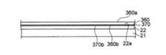
まず、図6に示すように、対向する一対の面360a,360bのうちの少なくとも一方の面360bが粗面となっている金属箔360を準備する。金属箔360は、線状導電体31の導電性金属層36を形成するようになる。金属箔360としては、例えば、金、銀、銅、白金、アルミニウム、クロム、モリブデン、ニッケル、チタン、パラジウム、インジウム、タングステン、及び、これらの合金の箔を用いることができる。また、金属箔360の厚さは、1μm以上60μm以下とすることができる。少なくとも一方の面360bが粗面となっている金属箔360は、金属箔360の作製時に少なくとも一方の面360bが粗面となったものを用いてもよいし、金属箔360の作成後に、少なくとも一方の面360bに公知の粗面化処理を行ったものを用いてもよい。なお、電界めっきにより連続的に作製される金属箔では、通常、電界めっきを行う際の電極が粗面となっていることから、一方の面が粗面となる。金属箔360の粗面360bの表面粗さは、十点平均粗さRzで、0.5μm以上10μm以下であることが好ましく、0.5μm以上5μm以下であることがより好ましい。このような粗面360bを有する金属箔360によれば、後述の金属箔360の保持層22への積層・圧着工程で、保持層22の面22aの表面粗さを、適切に、十点平均粗さRzで、0.5μm以上10μm以下、更に好ましくは0.5μm以上5μm以下とすることができる。 First, as shown in FIG. 6, a
次に、図7に示されているように、金属箔360の粗面360bに、線状導電体31の第1の暗色層37を形成するようになる暗色膜370を形成する。暗色膜370は、例えば金属箔360をなす材料の一部分に暗色化処理(黒化処理)を施して、金属箔360をなしていた一部分から、金属酸化物や金属硫化物からなる暗色膜370を形成することができる。また、暗色材料の塗膜や、ニッケルやクロム等のめっき層等のように、金属箔360の粗面360bの表面に暗色膜370を設けるようにしてもよい。以上のようにして作製された暗色膜370の表面は、金属箔360の粗面360bに対応し、粗面370bとして形成される。 Next, as illustrated in FIG. 7, a
次に、図8に示すように、基材フィルム21上に保持層22を形成し、この保持層22の基材フィルム21と対向する面と反対側の面22aと、暗色膜370の粗面370bとが対向するようにして、金属箔360及び暗色層370の積層物を保持層22上に積層する。基材フィルム21としては、例えば、0.03mm以上0.20mm以下の厚さを有する、ポリエチレンテレフタレート、ポリエチレンナフタレート、ポリカーボネート、ポリスチレン、環状ポリオレフィン等を用いることができる。保持層22は、例えば、基材フィルム21上に接着性または粘着性(タック性)を有する樹脂シートを基材フィルム21上に積層したり、基材フィルム21上に樹脂材料を塗布した後にこの樹脂材料を半硬化状態として、接着性または粘着性(タック性)を有するようにして、形成することができる。 Next, as shown in FIG. 8, the holding
次に、保持層22の基材フィルム21と対向する面と反対側の面(上面)22aと、金属箔360及び暗色膜370の積層物の粗面370bと、が対向するように、保持層22上に金属箔360及び暗色膜370の積層物を積層する。その後、金属箔360及び暗色膜370の積層物を保持層22に向かって押圧する。この押圧により、暗色層370の粗面370bと接する保持層22の上面22aをなす樹脂材は、暗色層370の粗面370bの微細な凹凸の内部に入り込む。これにより、保持層22の上面22aに暗色層370の粗面370bが転写され、保持層22の上面22aは粗面として形成される。そして、この状態で加熱や電離放射線の照射等により保持層22を硬化させると、いわゆるアンカー効果により、図9に示されているように、金属箔360と保持層22とが強固に接合される。この保持層22の上面22aの表面粗さは、十点平均粗さRzで、0.5μm以上10μm以下、更に好ましくは0.5μm以上5μm以下となっている。 Next, the holding
次に、図10に示すように、金属箔360上に、レジストパターン39を設ける。レジストパターン39は、形成されるべきパターン導電体30のパターンに対応したパターンとなっている。ここで説明する方法では、最終的にパターン導電体30をなす箇所の上にのみ、レジストパターン39が設けられている。このレジストパターン39は、公知のフォトリソグラフィー技術を用いたパターニングにより形成することができる。 Next, as shown in FIG. 10, a resist
次に、図11に示すように、レジストパターン39をマスクとして、金属箔360及び暗色膜370をエッチングする。このエッチングにより、金属箔360及び暗色膜370がレジストパターン39と略同一のパターンにパターニングされる。この結果、パターニングされた金属箔360から、線状導電体31の一部をなすようになる導電性金属層36が形成される。また、パターニングされた暗色膜370から、線状導電体31の一部をなすようになる第1の暗色層37が形成される。 Next, as shown in FIG. 11, the
このとき、保持層22の基材フィルム21と対向する面と反対側の面(上面)22a、すなわち、保持層22の金属箔360に接していた上面22aのうち、上述のエッチングにより暗色膜370を含む金属箔360が除去された露出部分22a1が露出する。図示された例においては、この露出部分22a1は、前述のように金属箔360の粗面360bに対応した凹凸を有する暗色膜370の粗面370bに接して粗面となっている。そして、この粗面の凹凸の内部に入り込んでいた暗色膜370が金属箔360とともにエッチングにより除去されることにより、金属箔360が除去された部分22a1は、その表面粗さが十点平均粗さRzで、0.5μm以上10μm以下、更に好ましくは0.5μm以上5μm以下である粗面となって露出する。 At this time, out of the surface (upper surface) 22a opposite to the surface facing the
なお、エッチング方法は特に限られることはなく、公知の方法を採用することができる。公知の方法としては、例えば、エッチング液を用いるウェットエッチングや、プラズマエッチングなどが挙げられる。その後、図12に示すように、レジストパターン39を除去する。 The etching method is not particularly limited, and a known method can be employed. Known methods include, for example, wet etching using an etchant, plasma etching, and the like. Thereafter, as shown in FIG. 12, the resist
次に、導電性金属層36の第1の暗色層37と反対側の面31a及び側面31c,31dに第2の暗色層38を形成する。第2の暗色層38は、例えば導電性金属層36をなす材料の一部分に暗色化処理(黒化処理)を施して、導電性金属層36をなしていた一部分から、金属酸化物や金属硫化物からなる第2の暗色層38を形成することができる。また、暗色材料の塗膜や、ニッケルやクロム等のめっき層等のように、導電性金属層36の表面に第2の暗色層38を設けるようにしてもよい。また、導電性金属層36の表面を粗化して第2の暗色層38を設けるようにしてもよい。このようにして図13に示すような導電体付きシート20が作成される。 Next, the second
なお、パターン導電体30は、前述したように、透視性または視認性を確保する観点から、高い開口率(非被覆率)にて開口33(又は間隙35のような非被覆部)を形成している。このため、図3に示すように、接合層13と導電体付きシート20の保持層22とは、パターン導電体30の開口33を介して接触している。ここで、保持層22の第1ガラス11に対向する露出部分(露出面)22aのうち、少なくとも接合層13に対面する露出部分22a1の表面粗さは、十点平均粗さRzで、0.5μm以上10μm以下、更に好ましくは0.5μm以上5μm以下となっている。このような表面粗さを有する保持層22は、保持層22の上面22aのうち、少なくとも被接合面22a1に、微細な凹凸を有する。そして、この微細な凹凸の内部に接合層13が入り込み、その状態で接合層13が硬化することで、いわゆるアンカー効果により保持層22の被接合面22a1と接合層13とが強固に接合される。 In addition, as described above, the
最後に、図14のように、パターン導電体30の側から接合層13及びガラス11を積層して、導電体付きシート20とガラス11とを接合する。同様に、基材フィルム21の側から接合層14及びガラス12を積層して、導電体付きシート20とガラス12とを接合する。これにより、図3に示した発熱板10が作製される。 Finally, as shown in FIG. 14, the
ところで、本件発明者らが研究を行ったところ、従来の方法で製造される導電体付きシートを含んだ発熱板には、白濁が生じ得ることがあった。とりわけ、パターン導電体が金属箔をパターニングすることによって得られる場合、より顕著に白濁が生じた。本件発明者らが鋭意検討を重ねたところ、この白濁は、発熱板内部での光の反射、より具体的には接合層と基材フィルムとの間での反射によるものであることが知見された。すなわち、従来の発熱板では、一対の接合層の間にタングステン配線が直接保持されていた。そして、接合層をなす材料として、ガラス板との間で大きな屈折率差を生じさせない材料が選択されてきた。このような従来の発熱板は、大きな屈折率差を有する屈折率界面を含まず、結果として、発熱板内での反射や屈折とった現象は生じにくくなっていた。 By the way, as a result of researches by the present inventors, white turbidity may occur in a heat generating plate including a sheet with a conductor manufactured by a conventional method. In particular, when the pattern conductor was obtained by patterning a metal foil, white turbidity was more noticeable. As a result of extensive studies by the present inventors, it has been found that this cloudiness is caused by reflection of light inside the heating plate, more specifically, reflection between the bonding layer and the base film. It was. That is, in the conventional heat generating plate, the tungsten wiring is directly held between the pair of bonding layers. A material that does not cause a large difference in refractive index between the glass plate and the glass plate has been selected as a material for forming the bonding layer. Such a conventional heat generating plate does not include a refractive index interface having a large refractive index difference, and as a result, a phenomenon such as reflection or refraction within the heat generating plate is less likely to occur.
このような発熱板では、接合層は、ガラスと導電体付きシートのパターン導電体を支持する基材部分との間に位置するようになる。したがって、物性やコスト面からの制約により、ガラスと導電体付きシートの基材部分との間に屈折率差が生じていれば、当然に、接合層とガラスとの間、および、接合層と基材部分との間に屈折率界面が生じるようになる。したがって、発熱板の内部において、反射や屈折が引き起こされ、この結果として、白濁感が生じていた。とりわけ、パターン導電体が金属箔をパターンニングすることによって得られる場合には、上述したように、基材部分のパターン導電体を支持する表面が凹凸面として形成され得る。この発熱板の内部では、拡散が生じるため、白濁感がより顕著になっていたものと推測される。 In such a heat generating plate, the bonding layer is positioned between the glass and the base material portion that supports the pattern conductor of the sheet with the conductor. Therefore, if there is a difference in refractive index between the glass and the base material portion of the sheet with the conductor due to restrictions from physical properties and cost, naturally, between the bonding layer and the glass and between the bonding layer and A refractive index interface is generated between the substrate portion and the substrate portion. Therefore, reflection and refraction are caused inside the heat generating plate, and as a result, a cloudiness is generated. In particular, when the pattern conductor is obtained by patterning a metal foil, the surface supporting the pattern conductor of the base material portion can be formed as an uneven surface as described above. Since diffusion occurs inside the heat generating plate, it is assumed that the cloudiness is more prominent.
一方、本実施の形態では、上述したように、基材フィルム21の屈折率nx、及び、接合層13,14の屈折率nyが、次の式(a)を満たすようになっている。
|nx−ny|<0.04 ・・・(a)
すなわち、接合層13,14との屈折率差が大きくならないように、基材フィルム21が選択されている。接合層13の屈折率nyと接合層14の屈折率nyは、同一の値となっていてもよいし異なる値となっていてもよいが、両者が式(a)を満たしていることが好ましい。Meanwhile, in the present embodiment, as described above, the refractive indices nx of the base film21, and the refractive index ny of the bonding layers 13 and 14 is adapted to satisfy the following formula (a) .
| Nx −ny | <0.04 (a)
That is, the
一般に、屈折率n1を有する媒質Aと、屈折率n2を有する媒質Bとの界面に垂直に入射する光の当該界面における反射率Rは、
R=(n1−n2)2/(n1+n2)2
である。すなわち、媒質Aと媒質Bと間の屈折率差が小さいほど急激に反射率Rが小さくなる。したがって、上述した式(a)を満たす場合には、接合層13,14と基材フィルム21との間を進む光の反射や屈折を効果的に抑制することができ、とりわけ、接合層14と基材フィルム21が隣接する場合には、接合層14と基材フィルム21との間に形成される界面での反射を直接的に低減し、屈折によるおおきな光路が生じないようにすることができる。これにより、白濁を効果的に低減することができる。In general, the reflectance R at the interface of light perpendicularly incident on the interface between the medium A having a refractive index n1 and the medium B having a refractive index n2 is
R = (n1 −n2 )2 / (n1 + n2 )2
It is. That is, as the refractive index difference between the medium A and the medium B is smaller, the reflectance R is rapidly decreased. Therefore, when satisfying the above-described formula (a), reflection and refraction of light traveling between the bonding layers 13 and 14 and the
加えて、本実施の形態において、上述したように、基材フィルム21の屈折率nxは、接合層14の屈折率ny、及び、保持層22の屈折率nzに対し、次の式(b)及び(c)のいずれかを満たすように設定される。
nz<nx<ny ・・・(b)
ny<nx<nz ・・・(c)
基材フィルム21の屈折率nxが、保持層22の屈折率nzと接合層14の屈折率nyとの間に設定されている場合、すなわち式(a)及び(b)のいずれかが満たされる場合、基材フィルム21が設けられていない場合と比べて、界面の数は増加するが、基材フィルム21を経由して保持層22と接合層14との間を進む光の合計の反射率を小さくすることができる。保持層22は、耐候性に加えて、所定の機能を発現することを意図されて設けられている。このような保持層22の材料選択の自由度は、一般に、基材フィルム21の材料選択の自由度よりも低くなる。上述した式(a)又は(b)が満たされるように基材フィルム21の材料を選択することにより、保持層22を設けた場合においても、基材フィルム21を介して保持層22と接合層14との間を進む光の反射や屈折による拡散を効果的に抑制することができる。これにより白濁を効果的に目立たなくすることができる。In addition, in this embodiment, as described above, the refractive indices nx of the
nz <nx <ny (b)
ny <nx <nz (c)
If the refractive indices nx of the
以上のように、本実施の形態における発熱板10は、一対のガラス11,12と、一対のガラス11,12の間に配置された導電体付きシート20と、各ガラス11,12と導電体付きシート20とを接合する一対の接合層13,14と、を備え、導電体付きシート20は、基材フィルム21と、基材フィルム21に支持され且つ線状導電体31を含むパターン導電体30と、を有しており、基材フィルムの屈折率nx及び接合層の屈折率nyが次の式(a)を満たしている。
|nx−ny|<0.04 ・・・(a)
このような発熱板10によれば、基材フィルム21と接合層13,14との間を進む光の反射を低減することができ、これにより白濁を効果的に目立たなくすることができる。As described above, the
| Nx −ny | <0.04 (a)
According to such a
また、本実施の形態における発熱板10は、一対のガラス11,12と、一対のガラス11,12の間に配置された導電体付きシート20と、各ガラス11,12と導電体付きシート20とを接合する一対の接合層13,14と、を備え、導電体付きシート20は、基材フィルム21と、基材フィルム21に支持され且つ線状導電体31を含むパターン導電体30と、基材フィルム21とパターン導電体30との間に設けられた保持層22と、を有しており、保持層22は、パターン導電体30をなす隣り合う線状導電体31の間となる領域において、接合層13と接触し、基材フィルム21の屈折率nx、接合層14の屈折率ny、及び、保持層22の屈折率nzが、次の式(b)及び(c)のいずれかを満たしている。
nz<nx<ny ・・・(b)
ny<nx<nz ・・・(c)
このような発熱板10によれば、基材フィルム21を介して保持層22と接合層14との間を進む光の反射率を低減することができ、これにより白濁を効果的に目立たなくすることができる。Moreover, the
nz <nx <ny (b)
ny <nx <nz (c)
According to such a
なお、前述した実施の形態に対して様々な変更を加えることが可能である。以下、図面を適宜参照しながら、変形例について説明する。以下の説明及び以下の説明で用いる図面では、上述した実施の形態と同様に構成され得る部分について、前述の実施の形態における対応する部分に対して用いた符号と同一の符号を用いることとし、重複する説明を省略する。 Various changes can be made to the above-described embodiment. Hereinafter, modified examples will be described with reference to the drawings as appropriate. In the following description and the drawings used in the following description, for parts that can be configured in the same manner as the above-described embodiment, the same reference numerals as those used for the corresponding parts in the above-described embodiment are used. A duplicate description is omitted.
図15に発熱体の変形例を示す。図15に示された例において、発熱板10は、一対のガラス11,12と、一対のガラス11,12の間に配置された導電体付きシート20と、各ガラス11,12と導電体付きシート20とを接合する一対の接合層13,14と、を備え、導電体付きシート20は、基材フィルム21と、基材フィルム21に支持され且つ線状導電体31を含むパターン導電体30と、を有している。つまり前述の実施の形態と異なり保持層22が設けられていない。この例において、基材フィルム21の屈折率nx、及び、接合層13,14の屈折率nyが、次の式(a)を満たすとき、発熱板10に生じる白濁を効果的に目立たなくすることができる。
|nx−ny|<0.04 ・・・(a)FIG. 15 shows a modification of the heating element. In the example shown in FIG. 15, the
| Nx −ny | <0.04 (a)
さらに、前述した実施の形態において、金属箔360をパターニングしてパターン導電体30を作製する例を示したが、この例に限られない。蒸着等の他の成膜方法により保持層22上に作製された金属膜をパターニングすることによって、パターン導電体30が作製されるようにしてもよい。また、前述した実施の形態において、保持層22の接合層13に接触する面の表面粗さが、十点平均粗さRzで、0.5μm以上10μm以下である例を示したが、この例に限られない。これらの変形例によっても、白濁を効果的に目立たなくすることができる。 Furthermore, in the above-described embodiment, the example in which the patterned
前述した実施の形態において、発熱板10が曲面状に形成されている例を示したが、この例に限られず、発熱板10が、平板状に形成されていてもよい。 In the above-described embodiment, the example in which the
発熱板10は、自動車1のリアウィンドウ、サイドウィンドウやサンルーフに用いてもよい。また、自動車以外の、鉄道、航空機、船舶、宇宙船等の乗り物の窓に用いてもよい。 The
更に、発熱板10は、乗り物以外にも、特に室内と室外とを区画する箇所、例えばビルや店舗、住宅の窓等に使用することもできる。 Furthermore, the
なお、以上において前述した実施の形態に対するいくつかの変形例を説明してきたが、当然に、複数の変形例を適宜組み合わせて適用することも可能である。 In addition, although several modifications with respect to embodiment mentioned above were demonstrated above, naturally, it is also possible to apply combining several modifications suitably.
1 自動車
5 フロントウィンドウ
7 電源
10 発熱板
11 ガラス
12 ガラス
13 接合層
14 接合層
15 配線部
16 接続部
20 導電体付きシート
21 基材フィルム
22 保持層
30 パターン導電体
31 線状導電体
32 分岐点
33 開口
34 接続要素
35 間隙
36 導電性金属層
360 金属箔
37 第1の暗色層
370 暗色膜
38 第2の暗色層
39 レジストパターンDESCRIPTION OF
Claims (5)
Translated fromJapanese一対のガラスと、
前記一対のガラスの間に配置され、基材フィルムと、前記基材フィルムに支持され且つ線状導電体を含むパターン導電体と、前記基材フィルムと前記パターン導電体との間に設けられた保持層と、を有する導電体付きシートと、
各ガラスと前記導電体付きシートとを接合する一対の接合層と、を備え、
前記保持層は、前記パターン導電体をなす隣り合う前記線状導電体の間となる領域において、前記接合層と接触し、
前記基材フィルムの屈折率nx、前記接合層の屈折率ny、及び、前記保持層の屈折率nzが、次の式(b)を満たす、発熱板。
nz<nx<ny・・・(b)A heating plate that generates heat when a voltage is applied,
A pair of glasses;
Arranged between the pair of glasses, provided between the base film, the pattern conductor supported by the base film and including a linear conductor, and between the base film and the pattern conductor A sheet with a conductor having a holding layer;
A pair of bonding layers for bonding each glass and the sheet with the conductor, and
The holding layer is in contact with the bonding layer in a region between the adjacent linear conductors forming the pattern conductor,
Refractive indices nx of the basefilm, the refractive index ny in the bondinglayer, and a refractive index nz of the holding layer, satisfies the following formula(b), heating plate.
nz<nx<ny(b)
一対のガラスと、 A pair of glasses;
前記一対のガラスの間に配置され、基材フィルムと、前記基材フィルムに支持され且つ線状導電体を含むパターン導電体と、前記基材フィルムと前記パターン導電体との間に設けられた保持層と、を有する導電体付きシートと、 Arranged between the pair of glasses, provided between the base film, the pattern conductor supported by the base film and including a linear conductor, and between the base film and the pattern conductor A sheet with a conductor having a holding layer;
各ガラスと前記導電体付きシートとを接合する一対の接合層と、を備え、 A pair of bonding layers for bonding each glass and the sheet with the conductor, and
前記保持層は、前記パターン導電体をなす隣り合う前記線状導電体の間となる領域において、前記接合層と接触し、 The holding layer is in contact with the bonding layer in a region between the adjacent linear conductors forming the pattern conductor,
前記基材フィルムの屈折率n Refractive index n of the base filmxx、前記接合層の屈折率n, Refractive index n of the bonding layeryy、及び、前記保持層の屈折率nAnd the refractive index n of the holding layerzzが、次の式(b)及び(c)のいずれかを満たし、Satisfies either of the following formulas (b) and (c):
前記保持層の前記接合層に接触する面の表面粗さは、十点平均粗さRzで、0.5μm以上10μm以下である、発熱板。 The heating plate has a ten-point average roughness Rz of 0.5 μm or more and 10 μm or less as a surface roughness of the holding layer in contact with the bonding layer.
nnzz<n<Nxx<n<Nyy・・・(b)... (b)
nnyy<n<Nxx<n<Nzz・・・(c)... (c)
|n| nxx−n-Nyy|<0.04| <0.04・・・(a)... (a)
前記保持層は、前記金属箔を前記基材フィルムに接合する層である、請求項1〜3のいずれか一項に記載の発熱板。The pattern conductor is formed by patterning a metal foil,
The heating plate according toany one of claims 1 to3, wherein the holding layer is a layer that joins the metal foil to the base film.
Priority Applications (1)
| Application Number | Priority Date | Filing Date | Title |
|---|---|---|---|
| JP2014265994AJP6492655B2 (en) | 2014-12-26 | 2014-12-26 | Heating plate and vehicle |
Applications Claiming Priority (1)
| Application Number | Priority Date | Filing Date | Title |
|---|---|---|---|
| JP2014265994AJP6492655B2 (en) | 2014-12-26 | 2014-12-26 | Heating plate and vehicle |
Publications (2)
| Publication Number | Publication Date |
|---|---|
| JP2016124372A JP2016124372A (en) | 2016-07-11 |
| JP6492655B2true JP6492655B2 (en) | 2019-04-03 |
Family
ID=56357373
Family Applications (1)
| Application Number | Title | Priority Date | Filing Date |
|---|---|---|---|
| JP2014265994AActiveJP6492655B2 (en) | 2014-12-26 | 2014-12-26 | Heating plate and vehicle |
Country Status (1)
| Country | Link |
|---|---|
| JP (1) | JP6492655B2 (en) |
Families Citing this family (5)
| Publication number | Priority date | Publication date | Assignee | Title |
|---|---|---|---|---|
| DE112017004048T5 (en)* | 2016-08-12 | 2019-05-29 | AGC Inc. | LAMINATED GLASS |
| JP6686799B2 (en)* | 2016-08-31 | 2020-04-22 | 大日本印刷株式会社 | Vehicle glass device and method for manufacturing heating electrode sheet used in the device |
| WO2019230731A1 (en)* | 2018-05-30 | 2019-12-05 | リンテック株式会社 | Heat generating sheet |
| KR102402735B1 (en)* | 2018-07-10 | 2022-05-26 | 주식회사 엘지화학 | Heating film and method for manufacturing thereof |
| KR102402734B1 (en)* | 2018-07-10 | 2022-05-26 | 주식회사 엘지화학 | Heating film and method for manufacturing thereof |
Family Cites Families (9)
| Publication number | Priority date | Publication date | Assignee | Title |
|---|---|---|---|---|
| JPS49107311A (en)* | 1973-02-14 | 1974-10-11 | ||
| US5593786A (en)* | 1994-11-09 | 1997-01-14 | Libbey-Owens-Ford Company | Self-adhering polyvinyl chloride safety glass interlayer |
| US5886321A (en)* | 1996-12-19 | 1999-03-23 | Ppg Industries, Inc. | Arrangement for heating the wiper rest area of a vehicle windshield |
| JP2009302481A (en)* | 2008-06-17 | 2009-12-24 | Dainippon Printing Co Ltd | Method of manufacturing electromagnetic wave shield sheet |
| JP5690592B2 (en)* | 2008-10-21 | 2015-03-25 | 大日本印刷株式会社 | Optical sheet |
| JP2010251230A (en)* | 2009-04-20 | 2010-11-04 | Fujifilm Corp | Electric window glass |
| JPWO2012026311A1 (en)* | 2010-08-24 | 2013-10-28 | コニカミノルタ株式会社 | Film mirror, film mirror manufacturing method, and solar power generation reflector |
| JP5581183B2 (en)* | 2010-11-19 | 2014-08-27 | 富士フイルム株式会社 | Method for manufacturing touch panel and conductive film for touch panel |
| JP2014218103A (en)* | 2013-05-02 | 2014-11-20 | 株式会社レニアス | Resin glass for vehicle having heating layer, and method of manufacturing the same |
- 2014
- 2014-12-26JPJP2014265994Apatent/JP6492655B2/enactiveActive
Also Published As
| Publication number | Publication date |
|---|---|
| JP2016124372A (en) | 2016-07-11 |
Similar Documents
| Publication | Publication Date | Title |
|---|---|---|
| JP6295885B2 (en) | Laminated glass, vehicles and windows | |
| JP6492644B2 (en) | Heating plate and vehicle | |
| JP6492655B2 (en) | Heating plate and vehicle | |
| JP6379771B2 (en) | Laminated glass, mesh sheet and intermediate member for laminated glass | |
| JP2017183063A (en) | Laminated glass plate with heating electrode, and vehicle | |
| JP2017106983A (en) | Light control panel and window with light control panel | |
| JP2016141210A (en) | Heating plate, conductive pattern sheet, and vehicle equipped with the heating plate | |
| JP2016102056A (en) | Glass laminate and manufacturing method thereof | |
| JP2016102055A (en) | Glass laminate, pattern sheet and manufacturing method of glass laminate | |
| JP6589270B2 (en) | Intermediate member for heating plate | |
| JP2018138456A (en) | Laminated glass, glass with heating mechanism and vehicle | |
| JP6770702B2 (en) | Conductive heating elements, laminated glass and vehicles | |
| JP6569346B2 (en) | Transparent heating plate and window with transparent heating plate | |
| JP2017112105A (en) | Heating plate, sheet with conductor, and vehicle and building window | |
| JP7316535B2 (en) | Heat-generating conductor, heat-generating plate, and method for producing heat-generating conductor | |
| JP6311493B2 (en) | Laminated glass, glass with heating mechanism and vehicle | |
| JP2019197727A (en) | Heating plate, conductor-equipped film, and manufacturing method of heating plate | |
| JP6897706B2 (en) | Heat plate and vehicle | |
| JP2019135718A (en) | Conductive pattern sheet, heating plate, vehicle including heating plate, and method for manufacturing heating plate | |
| JP6818260B2 (en) | Intermediate member for heating plate | |
| JP6597574B2 (en) | Transparent heating plate, vehicle and building windows | |
| JP2016104681A (en) | Method for producing laminated glass, and laminated glass | |
| JP6540037B2 (en) | Heater plate and vehicle | |
| WO2020122141A1 (en) | Pattern conductor, pattern conductor with bus bar, plyboard, partition member, and moving body | |
| JP6828239B2 (en) | Vehicles with heating plates, conductive pattern sheets and heating plates |
Legal Events
| Date | Code | Title | Description |
|---|---|---|---|
| A621 | Written request for application examination | Free format text:JAPANESE INTERMEDIATE CODE: A621 Effective date:20171030 | |
| A977 | Report on retrieval | Free format text:JAPANESE INTERMEDIATE CODE: A971007 Effective date:20180720 | |
| A131 | Notification of reasons for refusal | Free format text:JAPANESE INTERMEDIATE CODE: A131 Effective date:20180727 | |
| A521 | Request for written amendment filed | Free format text:JAPANESE INTERMEDIATE CODE: A523 Effective date:20180921 | |
| TRDD | Decision of grant or rejection written | ||
| A01 | Written decision to grant a patent or to grant a registration (utility model) | Free format text:JAPANESE INTERMEDIATE CODE: A01 Effective date:20190205 | |
| A61 | First payment of annual fees (during grant procedure) | Free format text:JAPANESE INTERMEDIATE CODE: A61 Effective date:20190218 | |
| R150 | Certificate of patent or registration of utility model | Ref document number:6492655 Country of ref document:JP Free format text:JAPANESE INTERMEDIATE CODE: R150 |