JP6486078B2 - Light emitting device - Google Patents
Light emitting deviceDownload PDFInfo
- Publication number
- JP6486078B2 JP6486078B2JP2014236277AJP2014236277AJP6486078B2JP 6486078 B2JP6486078 B2JP 6486078B2JP 2014236277 AJP2014236277 AJP 2014236277AJP 2014236277 AJP2014236277 AJP 2014236277AJP 6486078 B2JP6486078 B2JP 6486078B2
- Authority
- JP
- Japan
- Prior art keywords
- light
- light emitting
- translucent
- emitting device
- resin
- Prior art date
- Legal status (The legal status is an assumption and is not a legal conclusion. Google has not performed a legal analysis and makes no representation as to the accuracy of the status listed.)
- Active
Links
Images


Classifications
- H—ELECTRICITY
- H01—ELECTRIC ELEMENTS
- H01L—SEMICONDUCTOR DEVICES NOT COVERED BY CLASS H10
- H01L25/00—Assemblies consisting of a plurality of semiconductor or other solid state devices
- H01L25/03—Assemblies consisting of a plurality of semiconductor or other solid state devices all the devices being of a type provided for in a single subclass of subclasses H10B, H10D, H10F, H10H, H10K or H10N, e.g. assemblies of rectifier diodes
- H01L25/04—Assemblies consisting of a plurality of semiconductor or other solid state devices all the devices being of a type provided for in a single subclass of subclasses H10B, H10D, H10F, H10H, H10K or H10N, e.g. assemblies of rectifier diodes the devices not having separate containers
- H01L25/075—Assemblies consisting of a plurality of semiconductor or other solid state devices all the devices being of a type provided for in a single subclass of subclasses H10B, H10D, H10F, H10H, H10K or H10N, e.g. assemblies of rectifier diodes the devices not having separate containers the devices being of a type provided for in group H10H20/00
- H01L25/0753—Assemblies consisting of a plurality of semiconductor or other solid state devices all the devices being of a type provided for in a single subclass of subclasses H10B, H10D, H10F, H10H, H10K or H10N, e.g. assemblies of rectifier diodes the devices not having separate containers the devices being of a type provided for in group H10H20/00 the devices being arranged next to each other
- F—MECHANICAL ENGINEERING; LIGHTING; HEATING; WEAPONS; BLASTING
- F21—LIGHTING
- F21Y—INDEXING SCHEME ASSOCIATED WITH SUBCLASSES F21K, F21L, F21S and F21V, RELATING TO THE FORM OR THE KIND OF THE LIGHT SOURCES OR OF THE COLOUR OF THE LIGHT EMITTED
- F21Y2105/00—Planar light sources
- F21Y2105/10—Planar light sources comprising a two-dimensional array of point-like light-generating elements
- F21Y2105/14—Planar light sources comprising a two-dimensional array of point-like light-generating elements characterised by the overall shape of the two-dimensional array
- H—ELECTRICITY
- H01—ELECTRIC ELEMENTS
- H01L—SEMICONDUCTOR DEVICES NOT COVERED BY CLASS H10
- H01L2224/00—Indexing scheme for arrangements for connecting or disconnecting semiconductor or solid-state bodies and methods related thereto as covered by H01L24/00
- H01L2224/73—Means for bonding being of different types provided for in two or more of groups H01L2224/10, H01L2224/18, H01L2224/26, H01L2224/34, H01L2224/42, H01L2224/50, H01L2224/63, H01L2224/71
- H01L2224/732—Location after the connecting process
- H01L2224/73201—Location after the connecting process on the same surface
- H01L2224/73203—Bump and layer connectors
- H01L2224/73204—Bump and layer connectors the bump connector being embedded into the layer connector
- H—ELECTRICITY
- H01—ELECTRIC ELEMENTS
- H01L—SEMICONDUCTOR DEVICES NOT COVERED BY CLASS H10
- H01L2924/00—Indexing scheme for arrangements or methods for connecting or disconnecting semiconductor or solid-state bodies as covered by H01L24/00
- H01L2924/0001—Technical content checked by a classifier
- H01L2924/0002—Not covered by any one of groups H01L24/00, H01L24/00 and H01L2224/00
- H—ELECTRICITY
- H10—SEMICONDUCTOR DEVICES; ELECTRIC SOLID-STATE DEVICES NOT OTHERWISE PROVIDED FOR
- H10H—INORGANIC LIGHT-EMITTING SEMICONDUCTOR DEVICES HAVING POTENTIAL BARRIERS
- H10H20/00—Individual inorganic light-emitting semiconductor devices having potential barriers, e.g. light-emitting diodes [LED]
- H10H20/80—Constructional details
- H10H20/85—Packages
- H10H20/851—Wavelength conversion means
- H—ELECTRICITY
- H10—SEMICONDUCTOR DEVICES; ELECTRIC SOLID-STATE DEVICES NOT OTHERWISE PROVIDED FOR
- H10H—INORGANIC LIGHT-EMITTING SEMICONDUCTOR DEVICES HAVING POTENTIAL BARRIERS
- H10H20/00—Individual inorganic light-emitting semiconductor devices having potential barriers, e.g. light-emitting diodes [LED]
- H10H20/80—Constructional details
- H10H20/85—Packages
- H10H20/855—Optical field-shaping means, e.g. lenses
Landscapes
- Engineering & Computer Science (AREA)
- Power Engineering (AREA)
- Microelectronics & Electronic Packaging (AREA)
- Physics & Mathematics (AREA)
- Condensed Matter Physics & Semiconductors (AREA)
- General Physics & Mathematics (AREA)
- Computer Hardware Design (AREA)
- Led Device Packages (AREA)
- Non-Portable Lighting Devices Or Systems Thereof (AREA)
- Led Devices (AREA)
Description
Translated fromJapanese本発明は、発光ダイオード(LED)などの発光素子を複数個用いた発光装置に関する。 The present invention relates to a light emitting device using a plurality of light emitting elements such as light emitting diodes (LEDs).
半導体発光素子は、通常、成長用基板上に、n型半導体層、発光層及びp型半導体層からなる半導体構造層を成長し、それぞれn型半導体層及びp型半導体層に電圧を印加するn電極及びp電極を形成して作製される。さらに、放熱性能の向上を図る半導体発光素子として、半導体構造層を成長用基板とは別の支持基板に接合した後、成長用基板を除去した半導体発光素子が知られている。また、例えば複数の半導体発光素子を実装基板上に固定し、さらに波長変換用の蛍光体層を形成した後、樹脂などで封止することによって、半導体発光装置が作製される。 In a semiconductor light emitting device, a semiconductor structure layer composed of an n type semiconductor layer, a light emitting layer and a p type semiconductor layer is usually grown on a growth substrate, and a voltage is applied to the n type semiconductor layer and the p type semiconductor layer, respectively. It is fabricated by forming an electrode and a p-electrode. Further, as a semiconductor light emitting device for improving heat dissipation performance, a semiconductor light emitting device is known in which a semiconductor structure layer is bonded to a support substrate different from a growth substrate and then the growth substrate is removed. Further, for example, a plurality of semiconductor light emitting elements are fixed on a mounting substrate, a phosphor layer for wavelength conversion is further formed, and then sealed with a resin or the like, thereby manufacturing a semiconductor light emitting device.
特許文献1には、基板と、基板上に搭載された複数の発光素子と、複数の発光素子を分離する遮光性の隔壁体と、隔壁体上に設けられた透光性板材と、素子空間を充填する波長変換体とを有し、透光性板材は隔壁体との接触部から光放射方向に延在する遮光膜を含む発光装置が開示されている。また、特許文献2には、基板と、基板に搭載された複数の発光素子と、発光素子に対応する貫通孔が形成された型枠と、型枠の貫通孔に配置された蛍光体フィルター板とを備えた照明装置が開示されている。 Patent Document 1 discloses a substrate, a plurality of light-emitting elements mounted on the substrate, a light-shielding partition that separates the plurality of light-emitting elements, a translucent plate provided on the partition, and an element space. A light-emitting device including a light-shielding film that extends in a light emission direction from a contact portion with a partition wall. Further, Patent Document 2 discloses a substrate, a plurality of light emitting elements mounted on the substrate, a mold having a through hole corresponding to the light emitting element, and a phosphor filter plate disposed in the through hole of the mold. A lighting device including the above is disclosed.
近年、自動車用ヘッドライトにおいて、前方の状況、すなわち対向車や前走車などの有無及びその位置に応じて配光形状をリアルタイムで制御する技術が注目されている。この技術によって、例えば走行用の配光形状すなわちハイビームでの走行中に対向車を検知した際には、ヘッドライトに照射される領域のうち、当該対向車の領域のみをリアルタイムで遮光することが可能となる。従って、ドライバに対して常にハイビームに近い視界を与えることができ、その一方で対向車に眩惑光(グレア)を与えることが防止される。このような配光可変型のヘッドライトシステムは、例えば、複数の発光素子をアレイ状に配置した発光装置を作製し、当該発光素子の各々への導通及び非導通をリアルタイムで制御することによって実現することができる。 2. Description of the Related Art In recent years, attention has been paid to a technology for controlling a light distribution shape in real time according to the situation ahead, that is, the presence or absence of an oncoming vehicle or a preceding vehicle, and the position thereof. With this technology, for example, when an oncoming vehicle is detected while traveling with a light distribution shape, that is, a high beam, only the area of the oncoming vehicle among the areas irradiated on the headlight can be shielded in real time. It becomes possible. Therefore, it is possible to always give the driver a field of view close to a high beam, and on the other hand, it is possible to prevent the oncoming vehicle from being dazzled. Such a variable light distribution type headlight system is realized by, for example, manufacturing a light emitting device in which a plurality of light emitting elements are arranged in an array, and controlling conduction and non-conduction to each of the light emitting elements in real time. can do.
しかし、一般に、複数の発光素子が並置された発光装置を光源として用いる場合、その照射像にはわずかな暗部(暗線)が形成されることがある。この暗部形成の主な原因は、並置された発光素子の隣接する素子との間に設けられた素子間領域(非発光領域)の存在である。この暗部の形成を抑制することを考慮すると、並置された素子間の距離は小さいことが好ましい。 However, generally, when a light-emitting device in which a plurality of light-emitting elements are juxtaposed is used as a light source, a slight dark portion (dark line) may be formed in the irradiated image. The main cause of this dark portion formation is the presence of an inter-element region (non-light-emitting region) provided between adjacent elements of the light-emitting elements arranged in parallel. In consideration of suppressing the formation of the dark part, it is preferable that the distance between the juxtaposed elements is small.
しかし、素子間の距離を小さくした場合、導通状態の素子から放出された光の一部が隣接する非導通状態の素子に伝播してしまう場合がある。このいわゆる光のクロストークによって、非導通状態の素子からも弱い光が放出されているような状態となる場合がある。複数の素子を用いる発光装置の様々な応用分野において、光のクロストークはないことが望ましい。 However, when the distance between the elements is reduced, part of the light emitted from the conductive element may propagate to the adjacent non-conductive element. Due to this so-called crosstalk of light, there is a case where weak light is emitted even from a non-conductive element. In various application fields of light emitting devices using a plurality of elements, it is desirable that there is no crosstalk of light.
本発明は上記した点に鑑みてなされたものであり、光のクロストークが大幅に抑制され、照射像において明暗を明確に区別することが可能な発光装置を提供することを目的としている。また、素子間領域に起因する暗部の形成が大幅に抑制された高性能かつ高輝度の発光装置を提供することを目的としている。 The present invention has been made in view of the above points, and an object of the present invention is to provide a light-emitting device in which light crosstalk is significantly suppressed and brightness and darkness can be clearly distinguished in an irradiated image. It is another object of the present invention to provide a high-performance and high-luminance light-emitting device in which formation of dark portions due to the inter-element region is significantly suppressed.
本発明による発光装置は、搭載基板と、搭載基板上にマトリクス状に並置された複数の発光素子と、複数の発光素子の各々を埋設するように複数の発光素子上に形成された透光樹脂と、透光樹脂上に形成され、各々が複数の発光素子の各々の上面全体を覆うように形成された複数の透光板と、隣接する透光板間において互いに対向する一方の透光板の側面及び他方の透光板の側面のうち、いずれか一方の側面を覆うように形成された遮光膜と、を有し、透光樹脂は、隣接する透光板間を充填するように形成された充填部を有することを特徴としている。
A light emitting device according to the present invention includes a mounting substrate, a plurality of light emitting elements juxtaposed in a matrix on the mounting substrate, and a translucent resin formed on the plurality of light emitting elements so as to embed each of the plurality of light emitting elements. And a plurality of light-transmitting plates formed on the light-transmitting resin and each covering the entire upper surface of each of the plurality of light-emitting elements, and one light-transmitting plate facing each other between adjacent light-transmitting plates among the side surfaces and the side surface of the other transparent plate in the light-shielding film formed to cover the one side,have alight-transmitting resin is formed so as to fill the adjacent light-transmitting plates It is characterizedby having a filled portion .
以下に本発明の実施例について詳細に説明する。 Examples of the present invention will be described in detail below.
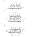
図1(a)は、実施例1の発光装置10の上面を模式的に示す図である。発光装置10は、搭載基板(以下、単に基板と称する場合がある)11上に複数の発光素子20(以下、単に素子と称する場合がある)がマトリクス状に並置された構造を有している。発光装置10は、その並置された複数の発光素子20の全体で発光領域EAを構成している。また、発光装置10の発光領域EAは、素子領域及び素子間領域からなる。ここでは、素子間領域とは素子とその隣接する素子との間の領域(空間)をいう。 FIG. 1A is a diagram schematically illustrating the upper surface of the
本実施例においては、搭載基板11に垂直な方向から見たとき、発光素子20の各々が矩形形状を有する場合について説明する。また、発光素子20が3行3列でマトリクス状に配列されており、全体として矩形の発光領域EAが構成されている場合について説明する。以下においては、複数の発光素子20のうち、隣接して整列した2つの特定の発光素子20を、発光素子20A及び20Bに区別して説明する。 In the present embodiment, the case where each of the
また、発光装置10は、各々が発光素子20の各々の上面全体を覆うように形成され、マトリクス状に並置された複数の透光板30を有している。透光板30の各々は、発光素子20の各々からの放出光に対して透光性を有している。透光板30の各々は、発光素子20の各々に対応した個数で配置され、全体として発光領域EAを構成している。発光装置10の発光領域EAは、その外縁が透光板30の側面によって画定される。 The
透光板30の各々は、本実施例においては3行3列でマトリクス状に並置されている。また、本実施例においては、透光板30の各々は、発光素子20の各々に対応した形状(例えば上面視において矩形形状)を有している。透光板30は、例えばサファイアなどを用いたガラス材料からなる。以下においては、発光素子20A及び20B上の透光板30の各々を、透光板30A及び30Bに区別して説明する。 Each of the light transmitting
発光素子20から放出された光は、透光板30の主面の一方に入射し、他方の主面から出射する。従って、具体的には、例えば素子20Aから放出された光は透光板30Aの下面に入射し、透光板30Aの上面全体から出射される。また、透光板30Aから出射された光は外部に取出される。発光装置10から取出される光は、透光板30の各々から出射された光となる。 The light emitted from the
図1(a)に示すように、発光装置10は、並置された複数の透光板30の各々のうちの隣接する透光板30A及び30B間において互いに対向する一方の透光板30Aの側面30AS及び他方の透光板30Bの側面30BSのうち、いずれか一方の側面(本実施例では側面30BS)を覆うように形成された遮光膜LBを有している。なお、図1(a)においては、図の明確さのため、遮光膜LBの形成領域にハッチングを施している。 As shown to Fig.1 (a), the light-
遮光膜LBは、例えばAg、Pt、Al、Rh及びTiなどの金属材料からなる。遮光膜LBは、素子20からの放出光に対して反射性又は吸収性を有する。すなわち、素子20から放出された光は、遮光膜LBによって反射又は吸収され、遮光膜LBを透過しない。なお、ここでは、互いに隣接する透光板30間の対向する側面(例えば側面30AS及び30BS)の全体を側面対PSと称する。 The light shielding film LB is made of a metal material such as Ag, Pt, Al, Rh, and Ti. The light shielding film LB has reflectivity or absorption with respect to the light emitted from the
発光装置10の発光領域EAは、遮光膜LBによって複数の発光セグメントESに区画される。本実施例においては、発光セグメントESは、各素子20、すなわち各透光板30に対応して形成されている。また、本実施例においては、各素子20の外縁によってではなく、透光板30の側面対PSの一方の側面に設けられた遮光膜LBによって画定される。すなわち、素子領域のみならず、素子間領域も発光セグメントESとして使用する。従って、素子間領域に対応する暗部が照射像に顕在化することが大幅に抑制される。また、発光セグメントESが遮光膜LBによって明確に画定されるため、素子間における光のクロストークが防止される。 The light emitting area EA of the
また、透光板30を設けることによって、発光領域EAにおける素子間領域上の領域の発光強度の低下を抑制することが可能となる。具体的には、複数の素子20を並置する場合、製造誤差や導通制御などを考慮すると、ある程度の間隔で素子20を配置する必要がある。従って、素子間領域自体を小さくすることには限界がある。しかし、透光板30の各々は、素子間の距離よりも小さい距離で配置することが可能である。本実施例においては、透光板30の各々は、素子20の上面よりも大きいサイズを有している。従って、透光板30間の距離は素子間領域よりも小さく、発光セグメントESのほぼ全域から均一な光を取出すことが可能となる。 In addition, by providing the
本実施例においては、素子20及び透光板30が矩形形状を有し、9つの素子20及び透光板30の各々がマトリクス状(格子状)に並置されている。また、透光板30は、少なくともその1つの側面30Sにおいて他の透光板30に隣接する。従って、行方向及び列方向にそれぞれ6つ、合計12個の側面対PSが構成されている。また、図1(a)に示すように、側面対PSの各々はその行方向及び列方向に整列して形成されている。また、遮光膜LBは、側面対PSのうち、同一側の側面の各々に形成されている。従って、例えば、列方向又は行方向に整列した複数の素子を一斉に発光させた場合には、照射像内に、一直線に形成された明暗の境界を表現することができる。 In the present embodiment, the
なお、本実施例においては、遮光膜LBが整列した側面対PS(例えば列方向に整列した3つの側面対PS)の各々における同一側の側面に形成される場合について説明した。しかし、遮光膜LBは、側面対PSのいずれか一方の側面に形成されていればよく、複数の遮光膜LBが直線状に整列する必要は無い。遮光膜LBの形成位置は、様々な用途(例えば照明用途)に応じて変更することができる。 In the present embodiment, the case where the light shielding film LB is formed on the same side surface in each of the aligned side surface pairs PS (for example, three side surface pairs PS aligned in the column direction) has been described. However, the light shielding film LB only needs to be formed on one side surface of the side surface pair PS, and the plurality of light shielding films LB need not be linearly aligned. The formation position of the light shielding film LB can be changed according to various applications (for example, illumination applications).
例えば、自動車用ヘッドライトを発光装置10によって構成する場合、その照射像の一部には、他の領域よりも大きな照射領域(発光セグメントES)を形成する必要が生ずる場合がある。この場合、素子20の形状を変更するのではなく、遮光膜LBの形成位置を調節することによって、発光セグメントESの大きさを調節することができる。具体的には、一部の透光板30の側面30Sには遮光膜LBを形成せず、当該遮光膜LBが形成されていない透光板30に隣接する透光板30の側面30Sのうち、当該遮光膜LBが形成されていない透光板30に対向する側面30Sの各々に遮光膜LBを形成する。これによって、当該遮光膜LBが形成されていない透光板30に対応する発光セグメントESの面積は、他の発光セグメントESの面積よりも大きなものとなる。 For example, when an automobile headlight is constituted by the
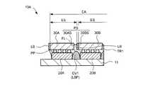
図1(b)は、発光装置10の構造を示す断面図である。図1(b)は、図1(a)のV−V線に沿った断面図である。基板11上には、発光素子20と透光板30との間において発光素子20の各々を埋設するように透光樹脂TRが形成されている。透光板30の各々は、透光樹脂TR上に形成され、それぞれ発光素子20の各々の上面を覆うように形成されている。また、透光樹脂TRは、発光素子20の各々の側面を覆うように形成されている。また、透光樹脂TRは、透光板30の下面全体を覆うように形成されている。また、透光樹脂TRは、隣接する透光板30間(例えば透光板30A及び30B間)を充填するように形成された充填部FLを有している。 FIG. 1B is a cross-sectional view showing the structure of the
透光樹脂TRは、例えばエポキシ樹脂、シリコン樹脂、ウレタン樹脂またはこれらを組み合わせたハイブリッド樹脂など、素子20からの放出光に対して透光性を有する材料を用いたペーストからなる。また、透光樹脂TRは、透光樹脂TR内に設けられた複数の蛍光体PPを有している。なお、図の明確さのため、蛍光体PPへのハッチングは省略している。蛍光体PPは、発光素子20からの光の波長を変換する。 The translucent resin TR is made of a paste using a material having translucency with respect to the light emitted from the
例えば、発光素子20が青色の発光波長を有する場合、その青色光を黄色光に変換する。この場合、透光板30には青色光及び黄色光が混色された擬似的な白色光が入射する。また、透光板30からは、この擬似的な白色光が出射し、外部に取出される。 For example, when the
蛍光体PPは、例えばYAG:Ce蛍光体(YAG(イットリウム・アルミニウム・ガーネット)に付活剤としてCe(セリウム)を導入した蛍光体)からなる。なお、蛍光体PPとして複数の種類の蛍光体を透光樹脂TRに含有させてもよい。また、取出されるべき光の波長(発光色)によっては、透光樹脂TRは蛍光体PPを有していなくてもよい。また、蛍光体PPは、透光板30内に設けられていてもよい。 The phosphor PP is made of, for example, a YAG: Ce phosphor (a phosphor obtained by introducing Ce (cerium) as an activator into YAG (yttrium, aluminum, garnet)). Note that a plurality of types of phosphors may be included in the translucent resin TR as the phosphor PP. Further, the translucent resin TR may not have the phosphor PP depending on the wavelength (light emission color) of the light to be extracted. Further, the phosphor PP may be provided in the
また、透光樹脂TRは、基板11上における隣接する素子20間(例えば素子20A及び20B間)の領域に延在する空洞CVを有している。また、空洞CVは、図1(b)に示すように、素子20の高さHEよりも大きな高さHCを有し、その上端が当該高さ方向における素子20と透光板30との間に位置している。空洞CVは、素子20間領域の短手方向に沿った断面において、略扇形の形状を有している。空洞CVは、基板11、素子20、透光板30によって囲まれた透光樹脂TRのペースト及び蛍光体PPが形成されていない(存在しない)部分である。 Further, the translucent resin TR has a cavity CV extending in a region between adjacent elements 20 (for example, between the
空洞CVは、隣接する素子20の側面全体を囲むように、素子間領域の全体に亘って形成されている。また、空洞CVは、素子20の高さ方向(厚さ方向)において隣接する素子20の側面のほぼ全域に亘って形成されている。素子20の側面から隣接する素子20に向かって放出された光は、空洞CVによって反射又は吸収され、素子20に向かって戻る又は減衰して消滅する。従って、例えば素子20Aの側面から素子20Bに向かって放出された光は、空洞CVによって反射又は吸収(減衰)される。すなわち、空洞CVは、素子20間の光のクロストークを防止する遮光体として機能する。 The cavity CV is formed over the entire inter-element region so as to surround the entire side surface of the
なお、空洞CVと透光板30の遮光膜LBと間の距離は小さいことが望ましい。具体的には、空洞CVと遮光膜LBとの間の領域は、素子間を光が伝播する隙間となる。従って、両者の距離は小さいほど素子20間の光のクロストークが抑制される。例えば空洞CVと遮光膜LBが接している場合、空洞CVと遮光膜LBとが一体となって素子20間のクロストークを抑制するための遮光壁として機能する。この場合、クロストーク抑制効果が最も高い。 It is desirable that the distance between the cavity CV and the light shielding film LB of the
また、透光樹脂TRは、素子20と透光板30との間を充填するように形成されている。また、透光樹脂TRは、発光素子20と透光板30との間において発光素子20を埋設するように形成されている。従って、素子20からの放出光の波長を均一に変換し、透光板30に入射させることが可能となる。 The translucent resin TR is formed so as to fill a space between the
また、透光樹脂TRは、隣接する透光板30間を充填するように形成された充填部FLを有している。すなわち、透光板30Aと隣接する透光板30Bの遮光膜LBとの間には透光樹脂TRが充填されている。従って、発光セグメントESは、透光板30と、隣接する透光板30間に設けられた透光樹脂TRとによって構成されている。すなわち、透光板30間の透光樹脂TRも発光セグメントの一部として使用することが可能となる。これによって、発光領域EAを透光板30に垂直な方向から見たとき、発光領域EAにおける暗部(暗線)を形成し得る部分は、ほぼ遮光膜LBの厚さ分だけとなる。従って、発光領域EAのほぼ全体が発光面となり、素子間領域に対応する暗部の形成を大幅に低減することが可能となる。 Further, the translucent resin TR has a filling portion FL formed so as to fill a space between adjacent
従って、光のクロストークの防止と素子間領域に対応する暗線の形成の防止との両立を実現することが可能となる。例えば、複数の並置された発光素子20を全て同時に導通させた場合は、照射像に暗線(ダークグリッド)が形成されることが防止される。一方、発光素子20の一部を導通させた場合、照射像における明暗が明確なものとなる。 Accordingly, it is possible to realize both prevention of light crosstalk and prevention of formation of dark lines corresponding to the inter-element region. For example, when all of the plurality of juxtaposed
次に、図2(a)〜(c)を用いて、発光装置10の製造方法について説明する。なお、図2(a)〜(c)は、発光装置10の製造中における図1(b)と同様の断面図である。まず、図1(a)に示すように、基板11上に発光素子20A及び20Bを含む複数の発光素子20をマトリクス状に形成する。次に、素子20A及び20Bの各々上に、蛍光体PPを含む樹脂ペーストTRA及びTRBを塗布する。 Next, a method for manufacturing the
続いて、図2(b)に示すように、一部の側面に遮光膜LBを形成した透光板30A及び30Bを準備し、これらを樹脂ペーストTRA及びTRBのそれぞれの上に配置する。このとき、隣接する側面対PSのいずれか1つの側面30Sが遮光膜LBを有するように透光板30の各々を配置する。 Subsequently, as shown in FIG. 2 (b),
なお、遮光膜LBは、透光板30としての例えばガラスの側面に、例えばAg、Al又はカーボンブラックなどの膜を蒸着又はメッキによって形成することで成膜することができる。なお、本実施例においては、平板形状を有し、その主面が正方形のガラスを準備し、その4つ側面のうちの2つの側面に遮光膜LBを形成した。なお、遮光膜LBは、素子20からの放出光に対して反射性及び吸収性を有する膜であればよいが、光の取出し効率の向上や発熱の防止を考慮すると、反射性を有することが望ましい。 The light shielding film LB can be formed by forming a film of, for example, Ag, Al, or carbon black on the side surface of the glass as the
そして、基板11を加熱しつつ、透光板30A及び30Bに圧力PWを加える。すると、素子20A及び20B上の樹脂ペーストTRA及びTRBの各々が素子20A及び20Bの上面全体に広がる。また、樹脂ペーストTRA及びTRBの各々は、その一部が素子20A及び20Bの側面にも漏れ広がる。また、樹脂ペーストTRA及びTRBの一部は、毛細管現象によって、透光板30A及び30Bの間にも入り込む。 Then, the pressure PW is applied to the
この状態で基板11を冷却することによって、樹脂ペーストTRA及びTRBを硬化させる。このようにして、図2(c)に示すように、素子20と透光板30との間及び隣接する透光板30間を充填し、素子20の側面を覆うように透光樹脂TRを形成することができる。樹脂ペーストTRA及びTRBは、紫外線照射や加熱によって硬化することも出来る。 By cooling the
なお、透光板30を素子20毎に個別に形成することで、発光セグメントESの設計自由度が向上する。具体的には、例えば透光板30の一部を異なるサイズ及び形状で形成することで、様々なサイズ及び形状の発光セグメントESを形成することが可能となる。また、素子20毎に、素子20の形状及びサイズとは無関係に発光セグメントESを形成することも可能となる。さらに、光学系の設計や照射シミュレーションなどが容易になる。 In addition, the design freedom of the light emission segment ES improves by forming the
また、透光板30を個別に形成することで、製造上の効果も大きい。具体的には、例えば透光板30を発光領域EA全体に1つ形成した場合に比べ、歩留まりが向上する。具体的には、透光板30を一体的に作成する場合、その一部の遮光膜LBの形成厚さなどの誤差、透光樹脂TR(樹脂ペーストTRA及びTRBなど)上への位置合わせの誤差によって、一体的に形成した透光板30の全体が不良品となる場合がある。一方、透光板30を個別に形成する場合は、個別に良品不良品の判定を行うことができるため、発光装置10全体の製造歩留まりへの影響は小さくなる。 Moreover, the effect on manufacture is also large by forming the
図3は、発光装置10の詳細構造を示す断面図である。図3は、図1(b)と同様の断面図であるが、透光樹脂TR及び透光板30を省略してある。発光素子20の各々(図3では20A及び20B)は、半導体構造層21と、p電極(第1の電極)25と、n電極(第2の電極)26と、を有する半導体発光素子である。以下においては、発光素子20が半導体発光素子である場合について説明する。すなわち、本実施例においては、発光装置10は半導体発光装置である場合について説明する。 FIG. 3 is a cross-sectional view showing a detailed structure of the
半導体構造層21は、発光層23がp型半導体層(第1の半導体層)22及びn型半導体層(第2の半導体層、第1の半導体層とは反対の導電型を有する半導体層)24に挟まれるように形成された構造を有している。半導体構造層21は、例えば、AlxInyGa1-x-yN(0≦x≦1、0≦y≦1)の組成を有するp型半導体層22、発光層23B及びn型半導体層24が搭載基板11上にこの順で順次積層された構造を有している。n型半導体層24の表面は光取出し面として機能する。In the
p電極25は、p型半導体層22上に形成され、反射性の高い金属からなる反射金属層27及び反射金属層27の全体を覆うように形成されたキャップ層28からなる。反射金属層27は、例えばAg、Pt、Ni、Al、Au及びPdなどの金属材料並びにこれらを含む合金を用いて形成される。キャップ層28は、例えばTi、W、Pt、Pd、Mo、Ru、Ir、Auなど、自身が他の層にマイグレーションしにくく、反射金属層27のマイグレーションを防止する金属材料を用いて形成される。なお、図示していないが、p型半導体層22及び反射金属層27間に、例えばITOやIZOなどの金属酸化膜を形成し、さらに光の反射性を高めることも可能である。 The p-
n電極26は、p型半導体層22側からp型半導体層22及び発光層23を貫通してn型半導体層24内に至り、n型半導体層24に接続されている。n電極26は、例えばTi、Al、Pt、Ag及びAuなどの金属材料を用いて形成される。また、半導体発光素子20の側面及び表面の各々には、絶縁保護膜29が形成されている。絶縁保護膜29は、例えばSiO2などの絶縁材料からなる。なお、反射金属層27上に形成されるキャップ層28として、電流拡散機能を有する電流拡散層を形成する場合、絶縁保護膜29が反射金属層27及びキャップ層28の金属材料のマイグレーションを防止する層として機能する。The n-
搭載基板11上にはp電極25に接続されたp側配線(第1の配線)12及びn電極26に接続されたn側配線(第2の配線)13が形成されている。具体的には、p側配線12は搭載基板11上に複数個設けられており、その各々は電気的に分離されている。例えば半導体発光素子20A及び20Bのp電極25の各々には、p側配線12A及び12Bが形成されている。また、p側配線12の各々は、搭載基板11と半導体発光素子20の各々との間において半導体発光素子20の各々のp電極25に接続されている。換言すれば、p側配線12は、その各々が半導体発光素子20のp型半導体層22に接続された個別配線として機能する。 A p-side wiring (first wiring) 12 connected to the p-
また、n側配線13は、搭載基板11と半導体発光素子20の各々との間において半導体発光素子20の各々のn電極25に接続されている。換言すれば、n型配線13は、半導体発光素子20の各々のn型半導体層24に接続された共通配線として機能する。n側配線13と、半導体発光素子20の各々におけるp電極25を含む半導体構造層21の搭載基板11側の表面との間には、その全面に絶縁層15が形成されている。n側配線13は、半導体発光素子20側に形成された第1の接合層(図示せず)及び搭載基板11側に形成された第2の接合層(図示せず)が接合された構造を有している。 Further, the n-
p側配線12及びn側配線13は、絶縁層14を介して互いに異なる階層で形成されている。具体的には、搭載基板11上に複数のp側配線12が並置されており、p側配線12を覆うように絶縁層14が形成されている。また、絶縁層14上にはn側配線13が形成されている。絶縁層14及び15における半導体発光素子20Aの直下の領域にはp側配線12Aに至る開口部が設けられ、当該開口部にはp電極25に接続されたビア電極12AVが形成されている。 The p-
同様に、半導体発光素子20Bのp電極25及び搭載基板11上のp側配線12Bは、ビア電極12BVを介して接続されている。また、ビア電極12AV及び12BVの各々は、半導体発光素子20側に形成された第1の接合層(図示せず)及び搭載基板11側に形成された第2の接合層(図示せず)が接合された構造を有している。以下においては、ビア電極12AV及び12BVを含むビア電極のいずれか1つを、ビア電極12Vと称する場合がある。 Similarly, the p-
また、絶縁層15における半導体発光素子20のn電極26が形成された領域上には、n電極26に至る開口部が設けられている。n電極26は、当該開口部を介してn側配線13に接続されている。 In addition, an opening reaching the
半導体発光装置10は、p側配線12及びn側配線13間において、半導体発光素子20の各々が互いに並列に接続された構造を有している。半導体発光素子20の各々は、p側配線12の各々への電流の印加を制御することによって、独立して導通状態及び非導通状態が制御される。すなわち、半導体発光素子20の各々は互いに独立して発光する。 The semiconductor
なお、搭載基板11の半導体発光素子20間の領域上には、素子間絶縁層16が形成されている。素子間絶縁層16は、例えばSiO2などの絶縁材料からなる。素子側面の絶縁保護膜29は、素子間絶縁層16上に形成されている。素子間絶縁層16は、発光装置の作製工程における半導体層を素子毎に分離する際のエッチング加工時において、搭載基板11上の配線などを保護する機能を有する。このようにして、半導体発光素子20の各々は、搭載基板11上に互いに並置され、また互いに並列に接続されている。An inter-element insulating
搭載基板11は、例えばSi、AlN、Mo、W、CuWなどの放熱性の高い材料からなる。絶縁層14及び15、絶縁保護膜29及び素子間絶縁層16は、例えばSiO2及びSi3N4などの絶縁材料からなる。第1及び第2の接合層、ビア電極12AV及び12BVは、その互いに接することとなる表面の材料が、Au及びSn、Au及びIn、Pd及びIn、Cu及びSn、Ag及びSn、Ag及びIn並びにNi及びSnなど、互いに融着して接合される材料の組み合わせか、又はAuなどの互いに拡散して接合される材料を用いて形成される。The mounting
なお、図示していないが、発光装置10は、搭載基板11を介して実装基板に実装され、ワイヤボンディングによって各素子の電極に電源が接続される。 Although not shown, the
図3に示すように、発光素子20の各々は、p電極25及びn電極26の両方がp型半導体層22側(搭載基板11側)に形成された構造を有している。従って、n型半導体層24の表面(光取出し面)の全体から光を取出すことが可能となる。一方、n電極26がp型半導体層22側に形成されることによって、発光層23の面積が小さくなる。具体的には、発光層23の一部がn電極26によって除去される。従って、発光層23の面内方向においては、発光強度(輝度)にムラが生ずることが懸念される。すなわち、発光セグメントES内での輝度ムラをもたらすことが懸念される。 As shown in FIG. 3, each of the
しかし、本実施例においては、素子20上に透光板30を設けることで、発光層23の近傍で生じた輝度ムラを低減することができる。従って、このような電極構成を有する発光素子20においては透光板30を設ける効果が大きい。すなわち、本実施例における発光素子20及び透光板30を組み合わせることで、発光セグメントES内においても輝度ムラのない発光装置10を提供することが可能となる。 However, in this embodiment, by providing the
なお、本実施例においては、発光装置10が透光樹脂TRを有する場合について説明したが、発光装置10は透光樹脂TRを有する場合に限定されない。また、透光樹脂TRは、素子20と透光板30との間を充填するように形成される場合について説明したが、透光樹脂TRは、素子20と透光板30との間を充填するように形成される場合に限定されない。素子20の各々上に透光樹脂TRが形成され、透光樹脂TR上に透光板30が形成されていればよい。また、透光樹脂TRは、透光板30間を充填するように形成されている場合に限定されない。また、透光樹脂TRは、素子20の側面を覆うように形成される場合に限定されない。 In the present embodiment, the case where the light-emitting
図4は、実施例1の変形例1に係る発光装置10Aの断面図である。なお、図4は、発光装置10Aにおける図1(b)と同様の断面図である。発光装置10Aは、透光樹脂TR1の構造を除いては、発光装置10と同様の構造を有している。 FIG. 4 is a cross-sectional view of the
本変形例においては、透光樹脂TR1の空洞CV1に遮光性を有する材料が充填されている。すなわち、透光樹脂TR1は、空洞部CV1が空洞CV1を充填するように形成された遮光部LBPを有している。遮光部LBPは、例えば遮光性(光反射性又は光吸収性)を有する樹脂材料からなる。遮光部LBPは、例えば、酸化チタン、酸化ニオブ、酸化タンタル、酸化ジルコニウム、硫酸バリウム、酸化アルミニウム、酸化珪素又は酸化亜鉛などを含有するペースト状のエポキシ樹脂又はシリコン樹脂からなる。遮光部LBPは、例えば発光装置10における空洞CVに上記したような遮光材料を充填することで形成することができる。 In this modification, the light-shielding material is filled in the cavity CV1 of the translucent resin TR1. That is, the translucent resin TR1 has a light shielding part LBP formed so that the cavity CV1 fills the cavity CV1. The light shielding portion LBP is made of, for example, a resin material having a light shielding property (light reflecting property or light absorbing property). The light shielding portion LBP is made of, for example, a paste-like epoxy resin or silicon resin containing titanium oxide, niobium oxide, tantalum oxide, zirconium oxide, barium sulfate, aluminum oxide, silicon oxide, zinc oxide, or the like. The light shielding portion LBP can be formed, for example, by filling the cavity CV in the
本変形例においては、空洞CV1が遮光部LBPを有することによって、素子20間のクロストークの抑制効果が向上する。すなわち、空洞CV1での遮光効果が向上する。実施例1における空洞CVは、空気又は封止ガス雰囲気によって構成されている。一方、本変形例においては、空洞CV1は、空洞CVに遮光部LBPを充填した遮光空洞として形成されている。従って、素子20間でのクロストーク防止効果の向上を図ることが可能となる。 In this modification, the cavity CV1 has the light shielding portion LBP, so that the effect of suppressing crosstalk between the
図5は、実施例1の変形例2に係る発光装置10Bの断面図である。図5は、発光装置10Bにおける図1(b)と同様の断面図である。発光装置10Bは、透光樹脂TR2の構造を除いては、発光装置10と同様の構造を有している。本変形例においては、透光樹脂TR2は、隣接する透光板30間を充填し、透光板30の上面と同一の高さ位置において平坦化された平坦部FLFを有している。 FIG. 5 is a cross-sectional view of the
本変形例は、透光樹脂TRにおける充填部FLのより好ましい形状を示す例である。本変形例においては、発光装置10における充填部FLの上面が透光板30の上面と同一の位置に設けられている。また、充填部FLの上面は平坦化されている。充填部FLがこのような平坦部FLFを有することによって、発光セグメントES内における取出し光の光量が均一化される。 This modification is an example showing a more preferable shape of the filling portion FL in the translucent resin TR. In the present modification, the upper surface of the filling portion FL in the
具体的には、本変形例においては、透光板30の各々は、その上面位置が同一の高さとなるように構成及び配置されている。また、平坦部FLF及び透光板30は同一の高さを有する上面を有している。従って、遮光膜LB間には透光性を有する部材である透光板30及び透光樹脂TRが一体的に形成されていると考えることができる。これによって、発光セグメントESは平坦な光取出し面を有することとなり、発光セグメントES内で均一な取出し光を得ることが可能となる。 Specifically, in the present modification, each of the
なお、平坦部FLFは、例えば、図2(c)において説明した樹脂ペーストTRA及びTRBの硬化前又は硬化後に、新たに樹脂ペーストを追加して透光板30間を完全に樹脂ペーストで充填した後、樹脂ペーストを平坦化することで形成することが可能である。また、すでに樹脂ペーストTRA及びTRBが透光板30間の領域に完全に充填されている場合、当該充填されている樹脂ペーストTRA及びTRBの上面を平坦化する(溢れ出ている部分を除去する)ことによっても、平坦部FLFを形成することができる。 For example, the flat portion FLF is completely filled with the resin paste by adding a new resin paste before or after the curing of the resin pastes TRA and TRB described in FIG. Then, it can be formed by flattening the resin paste. Further, when the resin pastes TRA and TRB are already completely filled in the region between the
また、平坦部FLFは、透光板30を素子20上に配置する前に形成することも可能である。例えば、透光板30を個別に準備した段階において、複数の透光板30の各々を樹脂ペーストによって一体化し、表面を平坦化する。そして、当該一体化した複数の透光板30を、透光樹脂TR2が形成された発光素子20の各々上に配置することで、平坦部FLFを有する透光樹脂TR2を有する発光装置10Bを形成することができる。 Further, the flat portion FLF can be formed before the
なお、透光板30間の透光樹脂TR2(すなわち充填部FL)は、その上面全体が平坦部FLFからなる場合に限定されない。透光樹脂TR2は、隣接する透光板30間を完全に充填し、その一部又は全部の上面に平坦部FLFを有していればよい。例えば、透光樹脂TR2は、透光板30の上面と同一の高さ位置に形成された平坦部FLFと、透光板30の上面を越えて突出する突出部を有していてもよい。 The translucent resin TR2 (that is, the filling portion FL) between the
なお、上記においては、発光素子20の各々が上面視において矩形形状を有する場合について説明したが、発光素子の上面視における形状はこれに限定されない。例えば、発光素子は、三角形や六角形の形状を有していてもよい。また、発光素子20の各々は、発光領域EAの暗部形成の抑制を考慮すると、平面充填形にて配列されていることが好ましい。また、発光素子20は、基板11に垂直な方向から見た場合に多角形状を有していればよい。 In the above description, the case where each of the
また、発光素子20の各々は、本実施例において示した構造ではなく、他の構造を有していてもよい。例えば、発光素子20の一部又は全部は、フリップチップ実装によって電極が電源に接続された構造を有していてもよい。また、上記においては、空洞CV及びCV1の下端は基板11の上面として形成されている。すなわち、基板11上の素子20間の領域は、透光樹脂TRが形成されず、その基板11の材料が露出している。しかし、発光素子20の形状や透光樹脂TRの塗布量によっては、透光樹脂TRが基板11上における素子20間の領域に部分的に又はその全体に形成されていてもよい。 In addition, each of the
また、透光板30の上面は、平坦面として形成されている場合について説明したが、透光板30の上面は、平坦面として形成されている場合に限定されない。例えば、光取出し効率を考慮すると、透光板30の上面は、凹凸構造を有していることが好ましい。例えば、透光板30の上面にサンドブラスト加工を行うことによって、透光板30の上面に凹凸を形成することができる。また、例えば、透光板30の上面に、部分的に樹脂部を形成することによって、透光板30の上面に凹凸を形成することができる。この場合、透光樹脂TRの充填部FLの表面は、透光板30と同様の凹凸構造を有していることが好ましい。 Moreover, although the case where the upper surface of the
また、透光板30のうち、最も外側の透光板30における他の透光板30に隣接しない側面部分においては、遮光膜LBは形成されていてもよく、形成されていなくてもよい。当該最外部は発光領域EAの外縁に対応する部分であるが、例えば、装置の照射像の輪郭を明確にすることが要求される用途においては、遮光膜LBが形成されていることが望ましい。 In addition, the light shielding film LB may or may not be formed on the side surface portion of the
本実施例においては、発光装置10は、マトリクス状に配列された素子20を有し、素子20上にマトリクス状に配列された透光板30を有する。また、隣接する透光板30間において互いに対向する一方の透光板30Aの側面30AS及び他方の透光板30Bの側面30BSのうち、いずれか一方の側面を覆うように形成された遮光膜LBを有している。従って、複数の並置された素子20を用いる発光装置において、素子20間での光のクロストークを抑制でき、また、素子間領域に対応する暗部の形成を抑制することができる。 In the present embodiment, the
10、10A、10B (半導体)発光装置
11 搭載基板
12 p側配線(第1の配線、個別配線)
13 n側配線(第2の配線、共通配線)
20、20A、20B (半導体)発光素子
21 半導体構造層
22 p型半導体層(第1の半導体層)
23 発光層
24 n型半導体層(第2の半導体層)
30、30A、30B 透光板
30S、30AS、30BS 側面
LB 遮光膜
TR 透光樹脂10, 10A, 10B (semiconductor) light emitting
13 n-side wiring (second wiring, common wiring)
20, 20A, 20B (Semiconductor) Light-emitting
23 Light emitting layer 24 n-type semiconductor layer (second semiconductor layer)
30, 30A, 30B
Claims (5)
Translated fromJapanese前記搭載基板上にマトリクス状に並置された複数の発光素子と、
前記複数の発光素子の各々を埋設するように前記複数の発光素子上に形成された透光樹脂と、
前記透光樹脂上に形成され、各々が前記複数の発光素子の各々の上面全体を覆うように形成された複数の透光板と、
隣接する前記透光板間において互いに対向する一方の透光板の側面及び他方の透光板の側面のうち、いずれか一方の側面を覆うように形成された遮光膜と、を有し、
前記透光樹脂は、前記隣接する透光板間を充填するように形成された充填部を有することを特徴とする発光装置。A mounting substrate;
A plurality of light emitting elements juxtaposed in a matrix on the mounting substrate;
A translucent resin formed on the plurality of light emitting elements so as to embed each of the plurality of light emitting elements;
A plurality of light-transmitting plates formed on the light-transmitting resin, each formed so as to cover the entire upper surface of each of the plurality of light-emitting elements;
Possess one side and the other side surface of the transparent plate adjacent the translucent plates one transparent plate facing each other in a light-shielding film formed to cover the one side,and
The light-transmitting resin has a filling portion formed so as to fill a space between the adjacent light-transmitting plates .
前記搭載基板上には、各々が前記第1の半導体層の各々に接続され、互いに電気的に分離された個別配線と、前記第2の半導体層の各々に接続された共通配線とが設けられていることを特徴とする請求項1に記載の発光装置。Each of the plurality of light emitting elements has a first semiconductor layer having a first conductivity type, a light emitting layer, and a second conductivity type opposite to the first conductivity type on the mounting substrate. A semiconductor structure layer having a structure in which the second semiconductor layer is sequentially stacked in this order;
On the mounting substrate, individual wirings are connected to each of the first semiconductor layers and electrically separated from each other, and common wirings connected to each of the second semiconductor layers are provided. The light-emitting device according to claim 1.
前記空洞は、前記隣接する前記発光素子の高さよりも大きな高さを有し、その上端が前記発光素子の高さ方向において前記発光素子と前記透光板との間に位置していることを特徴とする請求項1乃至3のいずれか1つに記載の発光装置。The translucent resin has a cavity extending in a region between the adjacent light emitting elements on the mounting substrate,
The cavity has a height greater than the height of the adjacent light emitting element, and an upper end thereof is located between the light emitting element and the light transmitting plate in a height direction of the light emitting element. The light emitting device according to any one of claims 1 to3 .
Priority Applications (2)
| Application Number | Priority Date | Filing Date | Title |
|---|---|---|---|
| JP2014236277AJP6486078B2 (en) | 2014-11-21 | 2014-11-21 | Light emitting device |
| US14/947,389US9570426B2 (en) | 2014-11-21 | 2015-11-20 | Semiconductor light-emitting device having matrix-arranged light-emitting elements and transparent plates |
Applications Claiming Priority (1)
| Application Number | Priority Date | Filing Date | Title |
|---|---|---|---|
| JP2014236277AJP6486078B2 (en) | 2014-11-21 | 2014-11-21 | Light emitting device |
Publications (2)
| Publication Number | Publication Date |
|---|---|
| JP2016100457A JP2016100457A (en) | 2016-05-30 |
| JP6486078B2true JP6486078B2 (en) | 2019-03-20 |
Family
ID=56010972
Family Applications (1)
| Application Number | Title | Priority Date | Filing Date |
|---|---|---|---|
| JP2014236277AActiveJP6486078B2 (en) | 2014-11-21 | 2014-11-21 | Light emitting device |
Country Status (2)
| Country | Link |
|---|---|
| US (1) | US9570426B2 (en) |
| JP (1) | JP6486078B2 (en) |
Cited By (1)
| Publication number | Priority date | Publication date | Assignee | Title |
|---|---|---|---|---|
| KR102651645B1 (en)* | 2023-05-12 | 2024-03-27 | 주식회사 금호에이치티 | Flexible slim planar light source |
Families Citing this family (11)
| Publication number | Priority date | Publication date | Assignee | Title |
|---|---|---|---|---|
| JP6428730B2 (en)* | 2016-08-24 | 2018-11-28 | 日亜化学工業株式会社 | Light emitting device |
| FR3061358B1 (en)* | 2016-12-27 | 2021-06-11 | Aledia | MANUFACTURING PROCESS OF AN OPTOELECTRONIC DEVICE INCLUDING PHOTOLUMINESCENT PHOTORESIN PLOTS |
| JP7082270B2 (en) | 2017-08-28 | 2022-06-08 | 日亜化学工業株式会社 | Light emitting device |
| JP7177336B2 (en)* | 2018-07-20 | 2022-11-24 | 日亜化学工業株式会社 | light emitting device |
| JP7323763B2 (en) | 2018-12-27 | 2023-08-09 | 日亜化学工業株式会社 | Light-emitting device and method for manufacturing light-emitting device |
| CN109556073B (en)* | 2018-12-31 | 2021-09-07 | 广州市诺思赛光电科技有限公司 | High-power LED car light |
| JP6947990B2 (en)* | 2019-04-22 | 2021-10-13 | 日亜化学工業株式会社 | Manufacturing method of light emitting device and light emitting device |
| KR102796591B1 (en)* | 2019-12-23 | 2025-04-22 | 서울반도체 주식회사 | Head lamp device |
| TWI720785B (en)* | 2020-01-15 | 2021-03-01 | 東貝光電科技股份有限公司 | Micro led light emitting device and manufacturing method thereof |
| JP7328557B2 (en) | 2020-11-30 | 2023-08-17 | 日亜化学工業株式会社 | Light source, light source device, and light source manufacturing method |
| JP7744597B2 (en)* | 2023-03-27 | 2025-09-26 | 日亜化学工業株式会社 | Light emitting device and manufacturing method thereof |
Family Cites Families (15)
| Publication number | Priority date | Publication date | Assignee | Title |
|---|---|---|---|---|
| JP2843219B2 (en)* | 1992-10-16 | 1999-01-06 | アルプス電気株式会社 | Light emitting element array device |
| JP3452982B2 (en)* | 1994-08-24 | 2003-10-06 | ローム株式会社 | LED print head, LED array chip, and method of manufacturing the LED array chip |
| JP2001326388A (en)* | 2000-05-12 | 2001-11-22 | Rohm Co Ltd | Semiconductor light-emitting device |
| JP2005093649A (en)* | 2003-09-17 | 2005-04-07 | Oki Data Corp | Semiconductor composite device, LED print head, and image forming apparatus using the same |
| EP2216834B1 (en)* | 2007-11-29 | 2017-03-15 | Nichia Corporation | Light-emitting apparatus |
| JP2009134965A (en) | 2007-11-29 | 2009-06-18 | Stanley Electric Co Ltd | LIGHTING DEVICE AND LIGHTING DEVICE MANUFACTURING METHOD |
| JP5622494B2 (en)* | 2010-09-09 | 2014-11-12 | スタンレー電気株式会社 | Light emitting device and manufacturing method thereof |
| JP2012169189A (en)* | 2011-02-15 | 2012-09-06 | Koito Mfg Co Ltd | Light-emitting module and vehicular lamp |
| JP5816031B2 (en) | 2011-09-05 | 2015-11-17 | 株式会社小糸製作所 | Vehicle headlamp device |
| JP5823211B2 (en) | 2011-09-01 | 2015-11-25 | 株式会社小糸製作所 | Vehicle headlamp device |
| DE102012101892B4 (en)* | 2012-03-06 | 2021-05-12 | OSRAM Opto Semiconductors Gesellschaft mit beschränkter Haftung | Wavelength conversion element, light-emitting semiconductor component and display device therewith as well as method for producing a wavelength conversion element |
| JP5965162B2 (en)* | 2012-03-08 | 2016-08-03 | スタンレー電気株式会社 | Light emitting device and manufacturing method thereof |
| JP6257513B2 (en)* | 2012-03-15 | 2018-01-10 | 株式会社小糸製作所 | Light emitting device and vehicle lamp |
| JP6153327B2 (en)* | 2013-01-22 | 2017-06-28 | シチズン電子株式会社 | LED module |
| JP2014179407A (en)* | 2013-03-14 | 2014-09-25 | Stanley Electric Co Ltd | Led light-emitting device, and lighting fixture for vehicle using the same |
- 2014
- 2014-11-21JPJP2014236277Apatent/JP6486078B2/enactiveActive
- 2015
- 2015-11-20USUS14/947,389patent/US9570426B2/enactiveActive
Cited By (1)
| Publication number | Priority date | Publication date | Assignee | Title |
|---|---|---|---|---|
| KR102651645B1 (en)* | 2023-05-12 | 2024-03-27 | 주식회사 금호에이치티 | Flexible slim planar light source |
Also Published As
| Publication number | Publication date |
|---|---|
| US9570426B2 (en) | 2017-02-14 |
| US20160148912A1 (en) | 2016-05-26 |
| JP2016100457A (en) | 2016-05-30 |
Similar Documents
| Publication | Publication Date | Title |
|---|---|---|
| JP6486078B2 (en) | Light emitting device | |
| JP6282493B2 (en) | Semiconductor light emitting device | |
| US11398464B2 (en) | Micro light emitting element and image display device | |
| KR102003001B1 (en) | Light emitting module | |
| US9153735B2 (en) | Optoelectronic semiconductor component | |
| JP2015156431A (en) | Semiconductor light emitting element and semiconductor light emitting device | |
| US10746356B2 (en) | Light emitting device | |
| JP2009177117A (en) | Display device | |
| KR101893199B1 (en) | Light-emitting device, light-emitting device module, and vehicle lighting unit | |
| JP6219177B2 (en) | Semiconductor light emitting device | |
| JP2017212301A (en) | LIGHT EMITTING DEVICE, LIGHTING DEVICE, VEHICLE LIGHTING DEVICE, AND LIGHT EMITTING DEVICE MANUFACTURING METHOD | |
| JP6570312B2 (en) | Semiconductor light emitting device and semiconductor light emitting device | |
| JP2015201473A (en) | Semiconductor light emitting device and method for manufacturing the same | |
| US20100127635A1 (en) | Optoelectronic device | |
| JP2015177181A (en) | light-emitting device | |
| JP2015177021A (en) | Semiconductor light emitting device | |
| JP6684541B2 (en) | Light emitting element | |
| JP2015159203A (en) | Semiconductor light emitting device | |
| JP2015201472A (en) | Semiconductor light emitting device and method for manufacturing the same | |
| JP2013026416A (en) | Element mounting substrate and light emitting device including the same | |
| JP2015103590A (en) | Semiconductor light emitting device | |
| EP4415063A1 (en) | Semiconductor light emitting device and semiconductor light emitting module | |
| JP2016207863A (en) | Light-emitting device | |
| KR102413435B1 (en) | Light emitting device and lighting apparatus having the same | |
| JP2018060939A (en) | Semiconductor light emitting device and manufacturing method thereof |
Legal Events
| Date | Code | Title | Description |
|---|---|---|---|
| A621 | Written request for application examination | Free format text:JAPANESE INTERMEDIATE CODE: A621 Effective date:20171011 | |
| A977 | Report on retrieval | Free format text:JAPANESE INTERMEDIATE CODE: A971007 Effective date:20180629 | |
| A131 | Notification of reasons for refusal | Free format text:JAPANESE INTERMEDIATE CODE: A131 Effective date:20180710 | |
| A521 | Request for written amendment filed | Free format text:JAPANESE INTERMEDIATE CODE: A523 Effective date:20180830 | |
| A131 | Notification of reasons for refusal | Free format text:JAPANESE INTERMEDIATE CODE: A131 Effective date:20181002 | |
| A521 | Request for written amendment filed | Free format text:JAPANESE INTERMEDIATE CODE: A523 Effective date:20181129 | |
| TRDD | Decision of grant or rejection written | ||
| A01 | Written decision to grant a patent or to grant a registration (utility model) | Free format text:JAPANESE INTERMEDIATE CODE: A01 Effective date:20190205 | |
| A61 | First payment of annual fees (during grant procedure) | Free format text:JAPANESE INTERMEDIATE CODE: A61 Effective date:20190219 | |
| R150 | Certificate of patent or registration of utility model | Ref document number:6486078 Country of ref document:JP Free format text:JAPANESE INTERMEDIATE CODE: R150 | |
| R250 | Receipt of annual fees | Free format text:JAPANESE INTERMEDIATE CODE: R250 | |
| R250 | Receipt of annual fees | Free format text:JAPANESE INTERMEDIATE CODE: R250 | |
| R250 | Receipt of annual fees | Free format text:JAPANESE INTERMEDIATE CODE: R250 | |
| R250 | Receipt of annual fees | Free format text:JAPANESE INTERMEDIATE CODE: R250 |