JP6479550B2 - Plasma processing equipment - Google Patents
Plasma processing equipmentDownload PDFInfo
- Publication number
- JP6479550B2 JP6479550B2JP2015087747AJP2015087747AJP6479550B2JP 6479550 B2JP6479550 B2JP 6479550B2JP 2015087747 AJP2015087747 AJP 2015087747AJP 2015087747 AJP2015087747 AJP 2015087747AJP 6479550 B2JP6479550 B2JP 6479550B2
- Authority
- JP
- Japan
- Prior art keywords
- processing apparatus
- mounting table
- plasma processing
- substrate
- flat plate
- Prior art date
- Legal status (The legal status is an assumption and is not a legal conclusion. Google has not performed a legal analysis and makes no representation as to the accuracy of the status listed.)
- Active
Links
- 238000012545processingMethods0.000titleclaimsdescription148
- 239000000758substrateSubstances0.000claimsdescription75
- 239000004020conductorSubstances0.000claimsdescription18
- PNEYBMLMFCGWSK-UHFFFAOYSA-Naluminium oxideInorganic materials[O-2].[O-2].[O-2].[Al+3].[Al+3]PNEYBMLMFCGWSK-UHFFFAOYSA-N0.000claimsdescription10
- 230000002093peripheral effectEffects0.000claimsdescription9
- VYPSYNLAJGMNEJ-UHFFFAOYSA-Nsilicon dioxideInorganic materialsO=[Si]=OVYPSYNLAJGMNEJ-UHFFFAOYSA-N0.000claimsdescription4
- 229910052581Si3N4Inorganic materials0.000claimsdescription3
- 238000000576coating methodMethods0.000claimsdescription3
- PMHQVHHXPFUNSP-UHFFFAOYSA-Mcopper(1+);methylsulfanylmethane;bromideChemical compoundBr[Cu].CSCPMHQVHHXPFUNSP-UHFFFAOYSA-M0.000claimsdescription3
- 239000010453quartzSubstances0.000claimsdescription3
- HQVNEWCFYHHQES-UHFFFAOYSA-Nsilicon nitrideChemical compoundN12[Si]34N5[Si]62N3[Si]51N64HQVNEWCFYHHQES-UHFFFAOYSA-N0.000claimsdescription3
- 239000011248coating agentSubstances0.000claimsdescription2
- 229910052814silicon oxideInorganic materials0.000claims1
- 229910052727yttriumInorganic materials0.000claims1
- VWQVUPCCIRVNHF-UHFFFAOYSA-Nyttrium atomChemical compound[Y]VWQVUPCCIRVNHF-UHFFFAOYSA-N0.000claims1
- 239000007789gasSubstances0.000description57
- 238000002347injectionMethods0.000description19
- 239000007924injectionSubstances0.000description19
- 238000004088simulationMethods0.000description16
- 239000012495reaction gasSubstances0.000description14
- 238000010926purgeMethods0.000description12
- 239000002243precursorSubstances0.000description10
- 238000010586diagramMethods0.000description8
- 238000009826distributionMethods0.000description8
- 238000001816coolingMethods0.000description7
- 238000000034methodMethods0.000description7
- 239000000463materialSubstances0.000description5
- 230000008569processEffects0.000description5
- QGZKDVFQNNGYKY-UHFFFAOYSA-NAmmoniaChemical compoundNQGZKDVFQNNGYKY-UHFFFAOYSA-N0.000description4
- 230000007246mechanismEffects0.000description4
- 238000007789sealingMethods0.000description4
- 230000006872improvementEffects0.000description3
- 229910052751metalInorganic materials0.000description3
- 239000002184metalSubstances0.000description3
- SIWVEOZUMHYXCS-UHFFFAOYSA-Noxo(oxoyttriooxy)yttriumChemical compoundO=[Y]O[Y]=OSIWVEOZUMHYXCS-UHFFFAOYSA-N0.000description3
- 238000012546transferMethods0.000description3
- XKRFYHLGVUSROY-UHFFFAOYSA-NArgonChemical compound[Ar]XKRFYHLGVUSROY-UHFFFAOYSA-N0.000description2
- IJGRMHOSHXDMSA-UHFFFAOYSA-NAtomic nitrogenChemical compoundN#NIJGRMHOSHXDMSA-UHFFFAOYSA-N0.000description2
- MROCJMGDEKINLD-UHFFFAOYSA-NdichlorosilaneChemical compoundCl[SiH2]ClMROCJMGDEKINLD-UHFFFAOYSA-N0.000description2
- 238000005516engineering processMethods0.000description2
- 230000006870functionEffects0.000description2
- 238000010438heat treatmentMethods0.000description2
- 238000012986modificationMethods0.000description2
- 230000004048modificationEffects0.000description2
- 239000002052molecular layerSubstances0.000description2
- QJGQUHMNIGDVPM-UHFFFAOYSA-Nnitrogen groupChemical group[N]QJGQUHMNIGDVPM-UHFFFAOYSA-N0.000description2
- 238000009832plasma treatmentMethods0.000description2
- 238000004904shorteningMethods0.000description2
- 238000007751thermal sprayingMethods0.000description2
- 239000000443aerosolSubstances0.000description1
- 229910052782aluminiumInorganic materials0.000description1
- XAGFODPZIPBFFR-UHFFFAOYSA-NaluminiumChemical compound[Al]XAGFODPZIPBFFR-UHFFFAOYSA-N0.000description1
- 229910021529ammoniaInorganic materials0.000description1
- 229910052786argonInorganic materials0.000description1
- KOPOQZFJUQMUML-UHFFFAOYSA-NchlorosilaneChemical compoundCl[SiH3]KOPOQZFJUQMUML-UHFFFAOYSA-N0.000description1
- 239000012141concentrateSubstances0.000description1
- 238000011109contaminationMethods0.000description1
- 229910052593corundumInorganic materials0.000description1
- 230000008021depositionEffects0.000description1
- 239000003989dielectric materialSubstances0.000description1
- 238000002474experimental methodMethods0.000description1
- 239000011261inert gasSubstances0.000description1
- 238000003780insertionMethods0.000description1
- 230000037431insertionEffects0.000description1
- 150000004767nitridesChemical class0.000description1
- 229910052757nitrogenInorganic materials0.000description1
- 229910000069nitrogen hydrideInorganic materials0.000description1
- 230000000149penetrating effectEffects0.000description1
- 230000000644propagated effectEffects0.000description1
- 239000003507refrigerantSubstances0.000description1
- 238000003860storageMethods0.000description1
- ZDHXKXAHOVTTAH-UHFFFAOYSA-NtrichlorosilaneChemical compoundCl[SiH](Cl)ClZDHXKXAHOVTTAH-UHFFFAOYSA-N0.000description1
- 239000005052trichlorosilaneSubstances0.000description1
- 229910001845yogo sapphireInorganic materials0.000description1
Images


Classifications
- H—ELECTRICITY
- H01—ELECTRIC ELEMENTS
- H01J—ELECTRIC DISCHARGE TUBES OR DISCHARGE LAMPS
- H01J37/00—Discharge tubes with provision for introducing objects or material to be exposed to the discharge, e.g. for the purpose of examination or processing thereof
- H01J37/32—Gas-filled discharge tubes
- H01J37/32431—Constructional details of the reactor
- H—ELECTRICITY
- H01—ELECTRIC ELEMENTS
- H01J—ELECTRIC DISCHARGE TUBES OR DISCHARGE LAMPS
- H01J37/00—Discharge tubes with provision for introducing objects or material to be exposed to the discharge, e.g. for the purpose of examination or processing thereof
- H01J37/02—Details
- H01J37/20—Means for supporting or positioning the object or the material; Means for adjusting diaphragms or lenses associated with the support
- H—ELECTRICITY
- H01—ELECTRIC ELEMENTS
- H01J—ELECTRIC DISCHARGE TUBES OR DISCHARGE LAMPS
- H01J37/00—Discharge tubes with provision for introducing objects or material to be exposed to the discharge, e.g. for the purpose of examination or processing thereof
- H01J37/32—Gas-filled discharge tubes
- H01J37/32431—Constructional details of the reactor
- H01J37/32798—Further details of plasma apparatus not provided for in groups H01J37/3244 - H01J37/32788; special provisions for cleaning or maintenance of the apparatus
- H01J37/32807—Construction (includes replacing parts of the apparatus)
Landscapes
- Chemical & Material Sciences (AREA)
- Analytical Chemistry (AREA)
- Physics & Mathematics (AREA)
- Engineering & Computer Science (AREA)
- Plasma & Fusion (AREA)
- Plasma Technology (AREA)
- Chemical Vapour Deposition (AREA)
Description
Translated fromJapanese本発明の種々の側面及び実施形態は、プラズマ処理装置に関する。 Various aspects and embodiments of the present invention relate to a plasma processing apparatus.
マイクロ波により励起された高密度プラズマを用いて被処理基板を処理するマイクロ波プラズマ処理装置が知られている。マイクロ波プラズマ処理装置は、例えば、多数のスロットが配列された平板状のアンテナを用いて処理装置内にマイクロ波を放射することにより、処理装置内により均一なマイクロ波を発生させることができる。これにより、マイクロ波プラズマ処理装置は、処理装置内に供給されたガスを電離させてより均一な高密度プラズマを生成することができる。 There is known a microwave plasma processing apparatus that processes a substrate to be processed using high-density plasma excited by microwaves. The microwave plasma processing apparatus can generate a uniform microwave in the processing apparatus by, for example, radiating the microwave into the processing apparatus using a flat antenna in which a large number of slots are arranged. Thereby, the microwave plasma processing apparatus can ionize the gas supplied in the processing apparatus and generate more uniform high-density plasma.
また、上記アンテナの下面には、誘電体で形成された誘電体窓が設けられる。該誘電体窓には、機械的な強度を確保するためにリブが形成されている。 A dielectric window formed of a dielectric is provided on the lower surface of the antenna. Ribs are formed on the dielectric window to ensure mechanical strength.
ところで、マイクロ波プラズマ装置において、被処理基板の膜質を向上させるためには、被処理基板の温度を高く設定するか、あるいは、アンテナと被処理基板との間の距離を短くすることが考えられる。しかし、被処理基板の温度を高く設定すると、下地層が熱によるダメージを受ける場合がある。そのため、アンテナと被処理基板との間の距離を短くすることで、被処理基板の膜質を向上させることが検討されている。しかし、上記したマイクロ波プラズマ装置では、誘電体窓の下面にリブが形成されているため、アンテナと被処理基板との間の距離を短くすることが困難である。 By the way, in the microwave plasma apparatus, in order to improve the film quality of the substrate to be processed, it is conceivable that the temperature of the substrate to be processed is set high or the distance between the antenna and the substrate to be processed is shortened. . However, if the temperature of the substrate to be processed is set high, the underlying layer may be damaged by heat. Therefore, it has been studied to improve the film quality of the substrate to be processed by shortening the distance between the antenna and the substrate to be processed. However, in the above microwave plasma apparatus, since the rib is formed on the lower surface of the dielectric window, it is difficult to shorten the distance between the antenna and the substrate to be processed.
本発明の一側面におけるプラズマ処理装置は、マイクロ波のプラズマを用いて処理容器内で被処理基板を処理するプラズマ処理装置であって、載置台と、アンテナとを備える。載置台は、処理容器内に設けられ、被処理基板を載置する。アンテナは、載置台と対向するように載置台の上方に設けられ、誘電体板を有し、誘電体板を介して処理容器内にマイクロ波を放射することにより、処理容器内に供給された処理ガスのプラズマを生成する。誘電体板は、アンテナの下面に設けられ、少なくとも載置台と対向する側の面が平面状に形成された平板部と、平板部において載置台と対向する側の面と反対側の面に形成されたリブとを有する。 A plasma processing apparatus according to one aspect of the present invention is a plasma processing apparatus that processes a substrate to be processed in a processing container using microwave plasma, and includes a mounting table and an antenna. The mounting table is provided in the processing container and mounts a substrate to be processed. The antenna is provided above the mounting table so as to face the mounting table, has a dielectric plate, and is supplied into the processing container by radiating microwaves into the processing container through the dielectric plate. A plasma of a processing gas is generated. The dielectric plate is provided on the lower surface of the antenna, and is formed on at least a flat plate portion where the surface facing the mounting table is formed in a flat shape, and a surface opposite to the surface facing the mounting table in the flat plate portion. Rib.
本発明の種々の側面および実施形態によれば、アンテナの機械的強度を確保しつつ、アンテナと被処理基板との間の距離を短くすることができる。 According to various aspects and embodiments of the present invention, the distance between the antenna and the substrate to be processed can be shortened while ensuring the mechanical strength of the antenna.
開示するプラズマ処理装置は、1つの実施形態において、マイクロ波のプラズマを用いて処理容器内で被処理基板を処理するプラズマ処理装置であって、載置台と、アンテナとを備える。載置台は、処理容器内に設けられ、被処理基板を載置する。アンテナは、載置台と対向するように載置台の上方に設けられ、誘電体板を有し、誘電体板を介して処理容器内にマイクロ波を放射することにより、処理容器内に供給された処理ガスのプラズマを生成する。誘電体板は、アンテナの下面に設けられ、少なくとも載置台と対向する側の面が平面状に形成された平板部と、平板部において載置台と対向する側の面と反対側の面に形成されたリブとを有する。 In one embodiment, the disclosed plasma processing apparatus is a plasma processing apparatus that processes a substrate to be processed in a processing container using microwave plasma, and includes a mounting table and an antenna. The mounting table is provided in the processing container and mounts a substrate to be processed. The antenna is provided above the mounting table so as to face the mounting table, has a dielectric plate, and is supplied into the processing container by radiating microwaves into the processing container through the dielectric plate. A plasma of a processing gas is generated. The dielectric plate is provided on the lower surface of the antenna, and is formed on at least a flat plate portion where the surface facing the mounting table is formed in a flat shape, and a surface opposite to the surface facing the mounting table in the flat plate portion. Rib.
また、開示するプラズマ処理装置の1つの実施形態において、アンテナは、平板部において載置台と対向する側の面と反対側の面に接するように設けられ、マイクロ波を伝搬させる導体板を有してもよく、リブは、平板部において載置台と対向する側の面と反対側の面の中で、導体板が設けられていない領域に形成されてもよい。 Further, in one embodiment of the disclosed plasma processing apparatus, the antenna includes a conductor plate that is provided so as to be in contact with a surface opposite to the surface facing the mounting table in the flat plate portion, and that propagates microwaves. Alternatively, the rib may be formed in a region where the conductive plate is not provided in the surface opposite to the surface facing the mounting table in the flat plate portion.
また、開示するプラズマ処理装置の1つの実施形態において、リブは、平板部から上方に突出するように、平板部において載置台と対向する側の面と反対側の面の周縁に沿って形成されてもよい。 Further, in one embodiment of the disclosed plasma processing apparatus, the rib is formed along the peripheral edge of the surface opposite to the surface facing the mounting table in the flat plate portion so as to protrude upward from the flat plate portion. May be.
また、開示するプラズマ処理装置の1つの実施形態において、リブは、平板部において載置台と対向する側の面と反対側の面の周縁の全周に渡って、平板部に設けられていてもよい。 In one embodiment of the disclosed plasma processing apparatus, the rib may be provided on the flat plate portion over the entire periphery of the surface on the opposite side of the surface facing the mounting table in the flat plate portion. Good.
また、開示するプラズマ処理装置の1つの実施形態において、平板部の厚みは、誘電体板内におけるマイクロ波の波長をλとした場合に、λ/8から3λ/8の範囲内であってもよい。 In one embodiment of the disclosed plasma processing apparatus, the thickness of the flat plate portion may be in the range of λ / 8 to 3λ / 8, where λ is the wavelength of the microwave in the dielectric plate. Good.
また、開示するプラズマ処理装置の1つの実施形態において、リブの平板部からの高さは、平板部の厚みの2倍から4倍の範囲内であってもよい。 Moreover, in one embodiment of the disclosed plasma processing apparatus, the height of the rib from the flat plate portion may be in a range of 2 to 4 times the thickness of the flat plate portion.
また、開示するプラズマ処理装置の1つの実施形態において、リブの厚みは、平板部の厚みの1倍から1.5倍の範囲内であってもよい。 In one embodiment of the disclosed plasma processing apparatus, the thickness of the rib may be in the range of 1 to 1.5 times the thickness of the flat plate portion.
また、開示するプラズマ処理装置の1つの実施形態において、平板部は、載置台と対向する側の平面状の面に所定のコーティングが施されていてもよい。 Further, in one embodiment of the disclosed plasma processing apparatus, the flat plate portion may be provided with a predetermined coating on a planar surface on the side facing the mounting table.
また、開示するプラズマ処理装置の1つの実施形態において、平板部の下面と載置台に載置された被処理基板との距離は、平板部の厚みの3倍から4倍の範囲内であってもよい。 Further, in one embodiment of the disclosed plasma processing apparatus, the distance between the lower surface of the flat plate portion and the substrate to be processed placed on the mounting table is within a range of 3 to 4 times the thickness of the flat plate portion. Also good.
また、開示するプラズマ処理装置の1つの実施形態において、誘電体板は、アルミナ、石英、窒化アルミニウム、窒化シリコン、または酸化イットリウムで形成されていてもよい。 In one embodiment of the disclosed plasma processing apparatus, the dielectric plate may be formed of alumina, quartz, aluminum nitride, silicon nitride, or yttrium oxide.
また、開示するプラズマ処理装置の1つの実施形態において、載置台は、被処理基板が軸線の周囲を移動するよう軸線を中心に回転可能に設けられていてもよい。また、処理容器は、載置台の回転により軸線に対して被処理基板が移動する周方向に複数の領域に分けられていてもよい。また、アンテナは、複数の領域の中の一つの領域において、処理容器内にマイクロ波を放射することにより、処理容器内に供給された処理ガスのプラズマを生成してもよい。 In one embodiment of the disclosed plasma processing apparatus, the mounting table may be provided to be rotatable about the axis so that the substrate to be processed moves around the axis. Further, the processing container may be divided into a plurality of regions in the circumferential direction in which the substrate to be processed moves with respect to the axis line by the rotation of the mounting table. The antenna may generate plasma of the processing gas supplied into the processing container by radiating microwaves into the processing container in one of the plurality of regions.
また、開示するプラズマ処理装置の1つの実施形態において、アンテナは、軸線に沿う方向から見た場合の断面形状が、略正三角形状であってもよい。 Further, in one embodiment of the disclosed plasma processing apparatus, the antenna may have a substantially equilateral triangular cross section when viewed from a direction along the axis.
以下に、開示するプラズマ処理装置の実施形態について、図面に基づいて詳細に説明する。なお、本実施形態により開示される発明が限定されるものではない。また、各実施形態は、処理内容を矛盾させない範囲で適宜組み合わせることが可能である。 Hereinafter, embodiments of the disclosed plasma processing apparatus will be described in detail with reference to the drawings. In addition, the invention disclosed by this embodiment is not limited. In addition, the embodiments can be appropriately combined within a range that does not contradict processing contents.
(実施形態)
[プラズマ処理装置10]
図1は、プラズマ処理装置10を概略的に示す上面図である。図2は、図1に示すプラズマ処理装置10から処理容器12の上部部材12bを取り除いた状態を示す平面図である。図3は、図1および図2におけるプラズマ処理装置10のA−A断面図である。図4は、図3に向かって軸線Xの左側の部分の拡大断面図である。図5は、図3に向かって軸線Xの右側の部分の拡大断面図である。図1〜図5に示すプラズマ処理装置10は、主に、処理容器12、載置台14、第1のガス供給部16、排気部18、第2のガス供給部20、およびプラズマ生成部22を備える。本実施形態におけるプラズマ処理装置10は、例えばセミバッチ式の基板処理装置である。(Embodiment)
[Plasma processing apparatus 10]
FIG. 1 is a top view schematically showing the
処理容器12は、例えば図1に示すように、軸線Xを中心軸とする略円筒状の容器である。処理容器12は、処理室Cを内部に備える。処理室Cは、噴射部16aを備えたユニットUを含む。処理容器12は、例えば、アルマイト処理またはY2O3(酸化イットリウム)の溶射処理等の耐プラズマ処理が内面に施されたAl(アルミニウム)等の金属で形成される。プラズマ処理装置10は、処理容器12内に複数のプラズマ生成部22を有する。それぞれのプラズマ生成部22は、処理容器12の上方に、マイクロ波を出力するアンテナ22aを備える。図1および図2に例示するプラズマ処理装置10には、例えば3個のアンテナ22aが設けられるが、プラズマ処理装置10に設けられるアンテナ22aの数は、図1および図2に図示するものに限定されず、適宜変更されてもよい。 For example, as shown in FIG. 1, the
プラズマ処理装置10は、例えば図2に示すように、上面に複数の載置領域14aを有する載置台14を備える。載置台14は、軸線Xを中心軸とする略円板状の部材である。載置台14の上面には、被処理基板の一例である基板Wを載置する載置領域14aが、軸線Xを中心として同心円状に複数(図2の例では5個)形成される。基板Wは載置領域14a内に配置され、載置領域14aは、載置台14が回転した際、基板Wがズレないように基板Wを支持する。載置領域14aは、略円状の基板Wと略同形状の略円状の凹部である。載置領域14aの凹部の直径W1は、載置領域14aに載置される基板Wの直径と比べ、略同一である。すなわち、載置領域14aの凹部の直径W1は、載置される基板Wが凹部に嵌合し、載置台14が回転しても、遠心力により基板Wが嵌合位置から移動しないように基板Wを固定する程度であればよい。 As shown in FIG. 2, for example, the
プラズマ処理装置10は、処理容器12の外縁に、ロボットアーム等の搬送装置を介して、基板Wを処理室Cへ搬入し、基板Wを処理室Cから搬出するためのゲートバルブGを備える。また、プラズマ処理装置10は、載置台14の外縁の下方に、排気口22hを備える。排気口22hには、排気装置52が接続される。プラズマ処理装置10は、排気装置52の動作を制御することにより、処理室C内の圧力を、目的とする圧力に維持する。本実施形態において、処理室C内の圧力は、例えば1〜5Torrの範囲内に設定される。 The
処理容器12は、例えば図3に示すように、下部部材12aおよび上部部材12bを有する。下部部材12aは、上方に開口した略筒形状を有し、処理室Cを形成する側壁および底壁を含む凹部を形成する。上部部材12bは、略筒形状を有し、下部部材12aの凹部の上部開口を閉蓋することにより処理室Cを形成する蓋体である。下部部材12aと上部部材12bとの間の外周部には、処理室Cを密閉するための弾性封止部材、例えばOリング等が設けられてもよい。 For example, as shown in FIG. 3, the
プラズマ処理装置10は、処理容器12により形成される処理室Cの内部に、載置台14を備える。載置台14は、駆動機構24によって軸線Xを中心に回転駆動される。駆動機構24は、モータ等の駆動装置24aおよび回転軸24bを有し、処理容器12の下部部材12aに取り付けられる。 The
回転軸24bは、軸線Xを中心軸線とし、処理室Cの内部まで延在する。回転軸24bは、駆動装置24aから伝達される駆動力により軸線Xを中心に回転する。載置台14は、中央部分が回転軸24bにより支持される。よって、載置台14は、軸線Xを中心に、回転軸24bの回転に従って回転する。なお、処理容器12の下部部材12aと駆動機構24との間には、処理室Cを密閉するOリング等の弾性封止部材が設けられていてもよい。 The
プラズマ処理装置10は、処理室C内部の載置台14の下方に、載置領域14aに載置された基板Wを加熱するためのヒータ26を備える。具体的には、載置台14を加熱することで載置台14に載置された基板Wを加熱する。基板Wは、処理容器12に設けられたゲートバルブGを介して、図示しないロボットアーム等の搬送装置により処理室Cに搬入され、載置領域14aに載置される。また、基板Wは、搬送装置によりゲートバルブGを介して処理室Cから搬出される。 The
処理室Cは、例えば図2に示すように、軸線Xを中心とする円周上に配列された第1の領域R1および第2の領域R2を形成する。載置領域14aに載置された基板Wは、載置台14の回転にともない、第1の領域R1および第2の領域R2を順に通過する。 For example, as shown in FIG. 2, the processing chamber C forms a first region R1 and a second region R2 arranged on a circumference around the axis X. The substrate W placed on the
プラズマ処理装置10は、例えば図4に示すように、第1の領域R1の上方に、載置台14の上面に対面するように、第1のガス供給部16が配置される。第1のガス供給部16は、噴射部16aを備える。すなわち、処理室Cに含まれる領域のうち噴射部16aに対面する領域が第1の領域R1である。 In the
噴射部16aは、複数の噴射口16hを備える。第1のガス供給部16は、複数の噴射口16hを介して第1の領域R1へ前駆体ガスを供給する。前駆体ガスが第1の領域R1に供給されることにより、第1の領域R1を通過する基板Wの表面に、前駆体ガスの原子または分子が化学的に吸着する。前駆体ガスは、例えば、DCS(ジクロロシラン)やモノクロロシラン、トリクロロシラン等である。 The
第1の領域R1の上方には、載置台14の上面に対面するように、排気部18の排気口18aが設けられている。排気口18aは、噴射部16aの周囲に設けられる。排気部18は、真空ポンプなどの排気装置34の動作により、排気口18aを介して処理室C内のガスを排気する。 An
第1の領域R1の上方には、載置台14の上面に対面するように、第2のガス供給部20の噴射口20aが設けられている。噴射口20aは、排気口18aの周囲に設けられている。第2のガス供給部20は、噴射口20aを介して第1の領域R1へパージガスを供給する。第2のガス供給部20によって供給されるパージガスは、例えばAr(アルゴン)等の不活性ガスである。パージガスが基板Wの表面に噴射されることにより、基板Wに過剰に化学吸着した前駆体ガスの原子または分子(残留ガス成分)が基板Wから除去される。これにより、基板Wの表面に、前駆体ガスの原子または分子が化学吸着した原子層または分子層が形成されることになる。 Above the first region R1, an
プラズマ処理装置10は、噴射口20aからパージガスを噴射し、排気口18aより載置台14の表面に沿ってパージガスを排気する。これにより、プラズマ処理装置10は、第1の領域R1に供給される前駆体ガスが第1の領域R1の外に漏れ出すことを抑制する。また、プラズマ処理装置10は、噴射口20aからパージガスを噴射して排気口18aより載置台14の面に沿ってパージガスを排気するので、第2の領域R2に供給する反応ガスまたは反応ガスのラジカル等が第1の領域R1内に侵入することを抑制する。すなわち、プラズマ処理装置10は、第2のガス供給部20からのパージガスの噴射および排気部18からの排気により、第1の領域R1と、第2の領域R2とを分離する。 The
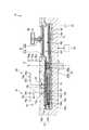
なお、プラズマ処理装置10は、噴射部16a、排気口18a、噴射口20aを含むユニットUを備える。すなわち、噴射部16a、排気口18a、および噴射口20aは、ユニットUを構成する部位として形成される。ユニットUは、例えば図4に示すように、第1の部材M1、第2の部材M2、第3の部材M3、および第4の部材M4が順次積み重ねられた構造を有する。ユニットUは、処理容器12の上部部材12bの下面に当接するように処理容器12に取り付けられる。 The
ユニットUには、例えば図4に示すように、第2の部材M2〜第4の部材M4を貫通するガス供給路16pが形成されている。ガス供給路16pは、上端が、処理容器12の上部部材12bに設けられたガス供給路12pと接続される。ガス供給路12pには、弁16vおよびマスフローコントローラ等の流量制御器16cを介して、前駆体ガスのガス供給源16gが接続される。また、ガス供給路16pの下端は、第1の部材M1と、第2の部材M2との間に形成された空間16dに接続される。空間16dには、第1の部材M1に設けられた噴射部16aの噴射口16hが接続される。 In the unit U, for example, as shown in FIG. 4, a
ユニットUには、第4の部材M4を貫通するガス供給路20rが形成される。ガス供給路20rは、上端が、処理容器12の上部部材12bに設けられたガス供給路12rと接続される。ガス供給路12rには、弁20vおよびマスフローコントローラ等の流量制御器20cを介して、パージガスのガス供給源20gが接続される。 In the unit U, a
ユニットUは、ガス供給路20rの下端が、第4の部材M4の下面と第3の部材M3の上面との間に設けられた空間20dに接続される。また、第4の部材M4は、第1の部材M1〜第3の部材M3を収容する凹部を形成する。凹部を形成する第4の部材M4の内側面と、第3の部材M3の外側面との間にはギャップ20pが設けられる。ギャップ20pは、空間20dに接続される。ギャップ20pの下端は、噴射口20aとして機能する。 In the unit U, the lower end of the
ユニットUには、第3の部材M3および第4の部材M4を貫通する排気路18qが形成される。排気路18qは、上端が、処理容器12の上部部材12bに設けられた排気路12qと接続される。排気路12qは、真空ポンプ等の排気装置34に接続される。また、排気路18qは、下端が、第3の部材M3の下面と、第2の部材M2の上面との間に設けられた空間18dに接続される。 In the unit U, an
第3の部材M3は、第1の部材M1および第2の部材M2を収容する凹部を備える。第3の部材M3が備える凹部を構成する第3の部材M3の内側面と、第1の部材M1および第2の部材M2の外側面との間には、ギャップ18gが設けられる。空間18dは、ギャップ18gに接続される。ギャップ18gの下端は、排気口18aとして機能する。プラズマ処理装置10は、噴射口20aからパージガスを噴射して排気口18aより載置台14の面に沿ってパージガスを排気することにより、第1の領域R1に供給する前駆体ガスが第1の領域R1の外へ漏れ出すことを抑制する。 The third member M3 includes a recess that accommodates the first member M1 and the second member M2. A
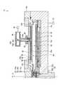
プラズマ処理装置10は、例えば図5に示すように、第2の領域R2の上方に設けられた上部部材12bの開口APに、載置台14の上面に対面するように設けられたプラズマ生成部22を備える。プラズマ生成部22は、アンテナ22aと、アンテナ22aにマイクロ波を供給する同軸導波管22bとを有する。本実施形態において、上部部材12bには例えば3つの開口APが形成され、プラズマ処理装置10は、例えば3つのプラズマ生成部22を備える。 For example, as shown in FIG. 5, the
プラズマ生成部22は、第2の領域R2へ、反応ガスおよびマイクロ波を供給して、第2の領域R2において反応ガスのプラズマを生成する。反応ガスに窒素含有ガスを用いた場合、プラズマ生成部22は、基板Wに化学的に吸着した原子層または分子層を窒化させる。反応ガスとしては、例えばN2(窒素)またはNH3(アンモニア)等の窒素含有ガスを用いることができる。 The
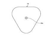
プラズマ生成部22は、例えば図5に示すように、開口APを閉塞するようにアンテナ22aを気密に配置する。アンテナ22aは、天板40、スロット板42、および遅波板44を有する。 For example, as shown in FIG. 5, the
図6および図7は、天板40の一例を示す図である。図6は、軸線Xに沿って天板40を上方から見た場合の天板40の形状の一例を示し、図7は、軸線Xに沿って天板40を下方から見た場合の天板40の形状の一例を示す。天板40は、誘電体により形成され、例えば図6および図7に示すように、平板部40aと、平板部40aの周縁に沿って平板部40aから上方に突出するリブ40bとを有する。本実施形態において、リブ40bは、平板部40aの周縁の全周に渡って平板部40a上に形成される。 6 and 7 are diagrams illustrating an example of the
本実施形態において、天板40は、例えば図6および図7に示すように、軸線Xの方向から見た場合の形状が、例えば角の丸い略正三角形状である。本実施形態において、天板40は、例えばアルミナで形成される。なお、天板40は、アルミナの他、石英、窒化アルミニウム、窒化シリコン、または酸化イットリウム等で形成されてもよい。天板40は、平板部40aの下面が処理容器12の上部部材12bに形成された開口APから第2の領域R2に露出するように上部部材12bによって支持されている。 In the present embodiment, for example, as shown in FIGS. 6 and 7, the
本実施形態の天板40では、少なくとも載置領域14aに載置された基板Wが通過する領域に対向する平板部40aの下面の領域が平面状に形成されている。そして、平面状に形成された平板部40aの下面の領域は、例えばAl2O3、Y2O3、またはYF2等によりコーティングされている。これらのコーティングは、溶射やエアロゾルデポジション法などによって行うことができる。これにより、基板Wの処理の過程で天板40の材料が基板Wの表面に付着することにより発生するコンタミネーションを防止することができる。また、本実施形態において、平板部40aの下面は平面状に形成されるため、平板部40aの下面にコーティングされる膜の密着性を向上させることができる。 In the
天板40上には、スロット板42が設けられている。スロット板42は、天板40のリブ40bで囲まれた領域内に配置されている。図8は、スロット板42の一例を示す図である。スロット板42は、金属により板状に形成される。スロット板42は、例えば図8に示すように、軸線Xの方向から見た場合の形状が、例えば角の丸い略正三角形状である。スロット板42には、例えば図8に示すように、複数のスロット対42cが形成されている。各スロット対42cには、互いに交差又は直交する方向に延びる長孔である二つのスロット孔42aおよび42bが含まれている。これらスロット対42cは、スロット板42の面内に半径の異なる同心円状に周方向に複数形成されている。また、スロット板42には、同軸導波管22bを配置するための開口42dが設けられる。スロット板42は、導体板の一例である。 On the
スロット板42上には遅波板44が設けられている。遅波板44は、天板40の遅波板44bで囲まれた領域内に配置されている。図9は、遅波板44の一例を示す図である。遅波板44は、例えばアルミナ等の誘電体で形成される。遅波板44は、例えば図9に示すように、軸線Xの方向から見た場合の形状が、例えば角の丸い略正三角形状である。遅波板44には、同軸導波管22bの外側導体62bを配置するための略円筒状の開口が設けられる。当該開口の周囲を形成する遅波板44の内径側の端部には、遅波板44の厚み方向に突出するリング状の突出部44aが設けられている。遅波板44は、突出部44aが上側に突出するように、スロット板42上に取り付けられる。 A
遅波板44の上面には冷却プレート46が設けられる。冷却プレート46は、その内部に形成された流路を流通する冷媒により、遅波板44を介してアンテナ22aを冷却する。冷却プレート46の表面は金属製である。冷却プレート46は、図示しないスパイラルスプリングガスケット等のバネにより遅波板44の上面に押圧されており、冷却プレート46の下面は、遅波板44の上面に密着している。これにより、アンテナ22aは、冷却プレート46を介して効率よく放熱することができる。 A cooling
同軸導波管22bは、中空の略円筒状の内側導体62aおよび外側導体62bを備える。内側導体62aは、アンテナ22aの上方から遅波板44の開口およびスロット板42の開口を貫通する。外側導体62bは、内側導体62aの外周面と、外側導体62bの内周面との間に隙間をあけて、内側導体62aを囲むように設けられる。外側導体62bの下端は、冷却プレート46の開口部に接続される。内側導体62aと外側導体62bとの間には、外側導体62bから内側導体62aの方向へ向かって、斜め下方向に複数のスタブ80が挿入されている。それぞれのスタブ80の挿入量を制御することにより、天板40の下面から第2の領域R2へ放射されるマイクロ波の分布を制御することができる。 The
プラズマ処理装置10は、導波管60および高周波発生器68を有する。高周波発生器68は、例えば1MHz〜3THzの帯域に含まれる高周波を発生させる。本実施形態において、高周波発生器68は、300MHz〜3THzの帯域に含まれるマイクロ波(例えば2.45GHzのマイクロ波)を発生させる。高周波発生器68が発生した、例えば約2.45GHzのマイクロ波は、導波管60を介して同軸導波管22bに伝搬し、内側導体62aと外側導体62bとの隙間を伝搬する。そして、遅波板44内を伝搬したマイクロ波は、スロット板42のスロット孔から天板40へ伝搬し、天板40から第2の領域R2へ放射される。 The
第2の領域R2には、反応ガス供給部22cから反応ガスが供給される。反応ガス供給部22cは、例えば開口APの周囲に延在するように、処理容器12の上部部材12bの内側に複数設けられ、反応ガスを天板40の下方に向けて噴射する。反応ガス供給部22cには、弁50vおよびマスフローコントローラ等の流量制御器50cを介して、反応ガスのガス供給源50gが接続される。 The reaction gas is supplied from the reaction
プラズマ生成部22は、反応ガス供給部22cにより第2の領域R2に反応ガスを供給し、アンテナ22aにより第2の領域R2にマイクロ波を放射する。これにより、第2の領域R2において反応ガスプラズマが生成される。 The
また、図3に示すように、プラズマ処理装置10は、プラズマ処理装置10の各構成要素を制御するための制御部70を備える。制御部70は、CPU(Central Processing Unit)等の制御装置、メモリ等の記憶装置、入出力装置等を備えるコンピュータであってもよい。制御部70は、メモリに記憶された制御プログラムに従ったCPUの動作に基づいて、プラズマ処理装置10の各構成要素を制御する。 As shown in FIG. 3, the
例えば、制御部70は、載置台14の回転速度を制御する制御信号を駆動装置24aへ出力する。また、制御部70は、基板Wの温度を制御する制御信号をヒータ26に接続された電源へ出力する。また、制御部70は、前駆体ガスの流量を制御する制御信号を弁16vおよび流量制御器16cへ出力する。また、制御部70は、排気量を制御する制御信号を排気装置34へ出力する。 For example, the
また、制御部70は、パージガスの流量を制御する制御信号を弁20vおよび流量制御器20cへ出力する。また、制御部70は、マイクロ波のパワーを制御する制御信号を高周波発生器68へ出力する。また、制御部70は、反応ガスの流量を制御する制御信号を弁50vおよび流量制御器50cへ出力する。また、制御部70は、排気口22hからの排気量を制御する制御信号を排気装置52へ送信する。 Further, the
[天板40の形状]
プラズマ処理装置10を用いた基板Wのプラズマ処理では、処理容器12内は、大気圧よりも低い圧力に設定される。そのため、天板40には、大気圧と処理容器12内の圧力との差圧に応じた圧力がかかる。そのため、天板40には、圧力に対する強度を確保するために、天板40にリブが設けられる場合がある。マイクロ波を用いたプラズマ処理では、アンテナ22aと基板Wとの間の距離が短くなると、基板Wに供給されるラジカルの量が増加し、基板W上に形成された膜の質が向上する。しかし、天板40の機械的な強度を確保するために、天板40の載置台14側の面にリブが設けられると、リブの高さの分、アンテナ22aを基板Wに近づけることが難しくなる。そのため、基板W上に形成された膜の質を向上させることが困難となる。[Shape of top plate 40]
In the plasma processing of the substrate W using the
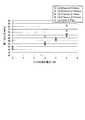
そこで、発明者らは、載置台14側の面にリブが設けられていない天板40を用いることを検討した。リブが設けられていない板状の天板を用いてプラズマ処理を実施した場合の天板の第一主応力をシミュレーションしたところ、図10に示すようなシミュレーション結果を得た。図10は、リブが設けられていない天板の第一主応力のシミュレーション結果の一例を示す図である。図10に示したシミュレーション結果では、11mm、13mm、および16mmの3通りの厚みL1の天板について、アンテナ22aから供給されるマイクロ波の電力を変えた場合の天板の第一主応力のシミュレーション結果が示されている。なお、図10に示したシミュレーション結果では、天板の材質としてアルミナを使用している。 Then, the inventors examined using the
図10の結果から明らかなように、いずれの厚みL1の天板においても、マイクロ波の電力が増加するに従って、天板の第一主応力が増加している。そして、厚みL1が11mmまたは13mmの天板では、5kWのマイクロ波を供給した場合の第一主応力が75MPaを超えている。また、厚みL1が16mmの天板では、5kWのマイクロ波を供給した場合の第一主応力が75MPa付近の値となっている。 As is apparent from the results of FIG. 10, the first principal stress of the top plate increases as the microwave power increases in any top plate of thickness L1. And in the top plate whose thickness L1 is 11 mm or 13 mm, the 1st main stress at the time of supplying a microwave of 5 kW exceeds 75 MPa. In the top plate having a thickness L1 of 16 mm, the first principal stress when a microwave of 5 kW is supplied is a value in the vicinity of 75 MPa.
ここで、本実施形態では、天板の過去の使用実績から、5kWのマイクロ波を供給した場合の第一主応力の上限値を75MPaと定めた。図10のシミュレーション結果を参照すると、厚みL1が11mmまたは13mmの天板では、5kWのマイクロ波を供給した場合の第一主応力が上限値を超えていることが分かる。また、厚みL1が16mmの天板では、5kWのマイクロ波を供給した場合の第一主応力が75MPa付近の値となっており、上限値に対してマージンがとれていないことが分かる。従って、リブが設けられていない板状の天板を用いた場合には、強度が確保できないことが分かった。 Here, in the present embodiment, the upper limit value of the first principal stress when a microwave of 5 kW is supplied is determined to be 75 MPa from the past use record of the top board. Referring to the simulation result of FIG. 10, it can be seen that the first principal stress when a microwave of 5 kW is supplied exceeds the upper limit value on a top plate having a thickness L1 of 11 mm or 13 mm. Moreover, in the top plate with a thickness L1 of 16 mm, the first principal stress when a microwave of 5 kW is supplied is a value near 75 MPa, and it can be seen that there is no margin with respect to the upper limit value. Therefore, it was found that the strength could not be secured when a plate-like top plate without ribs was used.
次に、リブが設けられた天板のシミュレーション結果について説明する。天板の載置台14側の面にリブが設けられると、リブの高さの分、アンテナ22aを基板Wに近づけることが難しくなる。そのため、本実施形態では、例えば図6および図7で説明したように、載置台14側の面と反対側の面の周縁全体にリブが設けられた天板40を用いる。 Next, the simulation result of the top plate provided with ribs will be described. If ribs are provided on the surface of the top plate on the mounting table 14 side, it is difficult to bring the
ここで、シミュレーションで用いたパラメータについて説明する。図11は、リブの高さおよび幅を説明する図である。図11に示すように、天板40において、平板部40aの厚みをL1、リブ40bの平板部40aからの高さをL2、リブ40bの幅をL3と定義する。 Here, parameters used in the simulation will be described. FIG. 11 is a diagram illustrating the height and width of the rib. As shown in FIG. 11, in the
なお、天板40の平板部40aは、スロット板42の下に配置される。そして、スロット板42に設けられたそれぞれのスロット孔42aおよび42bから放射されたマイクロ波は、天板40を伝搬し、天板40から第2の領域R2へ放射される。ここで、機械的な強度を上げるためには、天板40の厚みL1を増加させることが考えられる。しかし、天板40の厚みL1を増加させると、それぞれのスロット孔42aおよび42bから放射されたマイクロ波が、天板40の面内方向に広がりやすくなり、天板40上において、マイクロ波の定在波が発生しやすくなる。マイクロ波の定在波が発生すると、天板40の面内において、スロット孔42aおよび42bの直下とは異なる位置でマイクロ波が強まる場合がある。そのため、マイクロ波が、スロット孔42aおよび42bの配置とは異なる分布となり、マイクロ波の分布の制御性が低下する。これにより、プラズマの着火不良やプラズマ分布の偏りが発生する。そのため、平板部40aは、あまり厚すぎることも好ましくない。 The
本実施形態では、機械的な強度と、マイクロ波の分布の制御性の観点から、平板部40aの厚みL1は、天板40内のマイクロ波の波長をλとした場合に、例えばλ/8〜3λ/8の範囲内の厚みであることが好ましい。天板40の材質がアルミナである場合、2.45GHzのマイクロ波に対して、平板部40aの厚みL1は、例えば約5mm〜15mmの範囲内であることが好ましい。マイクロ波の分布の制御性の観点からは、平板部40aの厚みL1は、λ/4であることがより好ましい。天板40の材質がアルミナである場合、天板40内における2.45GHzのマイクロ波の波長は、約40mmであるため、マイクロ波の分布の制御性の観点からは、平板部40aの厚みL1は、約10mm程度であることが好ましい。しかし、機械的強度を考慮すると、約10mmの厚みでは、強度のマージンが少ないと考えられる。そのため、以下では、平板部40aの厚みL1を13mmとしてシミュレーションを行った。 In the present embodiment, from the viewpoint of mechanical strength and controllability of the microwave distribution, the thickness L1 of the
図12は、リブが設けられた天板40のシミュレーション結果の一例を示す図である。なお、図12に示したシミュレーション結果では、天板40の材質としてアルミナを使用している。 FIG. 12 is a diagram illustrating an example of a simulation result of the
図12のシミュレーション結果から明らかなように、リブ40bの高さL2が高くなる程、マイクロ波の強度の増加に対して、第一主応力の増加が抑えられている。しかし、リブ40bの高さL2が高くなり過ぎると、リブ40bと平板部40aとの接続部分に集中する応力が増加する傾向がある。そのため、リブ40bの高さL2は、所定範囲内であることが好ましく、例えば平板部40aの厚みL1の2倍〜4倍の範囲内であることが好ましい。本実施形態では、リブ40bの高さL2は、例えば20mm〜40mmの範囲内であることが好ましい。 As is apparent from the simulation results of FIG. 12, the increase in the first principal stress is suppressed with respect to the increase in the intensity of the microwave as the height L2 of the
また、図12のシミュレーション結果から明らかなように、リブ40bの幅L3が大きい程、マイクロ波の強度の増加に対して、第一主応力の増加が抑えられている。しかし、リブ40bの幅L3が大き過ぎると、スロット板42や遅波板44を配置するための平板部40aの領域が狭くなる。そのため、リブ40bの幅L3は、所定範囲内であることが好ましく、例えば平板部40aの厚みL1の1倍〜1.5倍の範囲内であることが好ましい。本実施形態では、リブ40bの幅L3は、例えば10mm〜15mmの範囲内であることが好ましい。 As is clear from the simulation results of FIG. 12, the increase in the first principal stress is suppressed as the microwave L increases as the width L3 of the
図12から明らかなように、シミュレーションでは、平板部40aの厚みL1を13mm、リブ40bの高さL2を27.5mm、リブ40bの幅L3を12.5mmに設定することにより、天板40に発生する第一主応力を62.9MPaまで抑えることができることが確認できた。 As is apparent from FIG. 12, in the simulation, the thickness L1 of the
このように、本実施形態では、例えば図5〜図7に示したように、載置台14側の面と反対側の面にリブが設けられた天板40を用いることにより、載置台14側の面にリブが設けられていない場合であっても、天板40に発生する第一主応力を所定値以下に抑えることができる。これにより、アンテナ22aと基板Wとの間の距離を短くすることができる。 As described above, in this embodiment, for example, as shown in FIGS. 5 to 7, by using the
例えば、下面にリブが形成された天板40を用いた従来のプラズマ処理装置10では、リブ以外の部分の天板40の下面から基板Wまでの距離が67mmであった。これに対し、本実施形態のプラズマ処理装置10では、天板40の下面から基板Wまでの距離を45.7mmまで短くすることができた。即ち、本実施形態のプラズマ処理装置10では、従来のプラズマ処理装置10と比べて、天板40から基板Wまでの距離を、21.3mm短縮することができる。 For example, in the conventional
このように、アンテナ22aと基板Wとの間の距離を短くすることにより、アンテナ22a付近で生成されたラジカルが、より基板Wに届きやすくなる。従って、基板Wに供給されるラジカルの量を増加させることができ、より低い処理温度でも、基板Wの膜質を向上させることが可能となる。 Thus, by shortening the distance between the
なお、天板40と基板Wとの間の距離は、あまり短くし過ぎると、基板Wにチャージアップダメージが発生する。実験では、天板40の下面と基板Wとの距離が30mm未満になった場合に、基板Wにチャージアップダメージが発生した。そのため、アンテナ22aと基板Wとの間の距離を短くし過ぎることも好ましくない。そのため、本実施例では、アンテナ22aと基板Wとの間の距離は、所定範囲内であることが好ましく、例えば平板部40aの厚みL1の3倍〜4倍の範囲内であることが好ましい。本実施形態では、アンテナ22aと基板Wとの間の距離は、例えば30mm〜40mmの範囲内であることが好ましい。 It should be noted that if the distance between the
以上、実施形態について説明した。本実施形態のプラズマ処理装置10によれば、基板Wの膜質を向上させることができる。特に、本実施形態のプラズマ処理装置10によれば、アンテナ22aの下面の天板40の厚みL1を3λ/8以下の厚みに維持したまま、天板40の下面を平坦にすることができるので、プラズマが生成される領域におけるマイクロ波の分布の制御性の向上と、基板Wに供給されるラジカルの量の増加とを両立することができる。 The embodiment has been described above. According to the
なお、開示の技術は、上記した実施形態に限定されるものではなく、その要旨の範囲内で数々の変形が可能である。 Note that the disclosed technique is not limited to the above-described embodiment, and various modifications can be made within the scope of the gist.
例えば、上記した実施形態では、アンテナ22aとして、軸線Xに沿う方向から見た場合の断面形状が、略正三角形状のアンテナ22aが用いられたが、開示の技術はこれに限られない。他の形態として、軸線Xに沿う方向から見た場合のアンテナ22aの形状は、略正三角形以外の形状、例えば略円状や多角形状等であってもよい。 For example, in the above-described embodiment, the
また、上記した実施形態では、プラズマ処理装置10として、セミバッチ式の基板処理装置を例に説明した。しかし、開示の技術はこれに限られない。例えば、枚葉式のプラズマ処理装置10に対しても、上記した天板40が用いられてもよい。 In the above-described embodiment, a semi-batch type substrate processing apparatus has been described as an example of the
また、上記した実施形態における天板40は、平板部40aの周縁の全周に渡って、リブ40bが設けられる。しかし、開示の技術はこれに限られない。例えば、リブ40bは、平板部40aの周縁の中で、一部の区間に設けられていなくてもよい。なお、軸線Xに沿う方向から見た場合の天板40の形状が、略正三角形状である場合、コーナー部分に応力が集中しやすい傾向がある。そのため、平板部40aの周縁の全周にリブ40bが設けられない場合であっても、該コーナー部分にはリブ40bが設けられることが好ましい。また、リブ40bは、平板部40aの周縁以外の部分に設けられていてもよい。 Moreover, the
また、リブ40bは、平板部40aの上面(載置台14と対向する側の面と反対側の面)に設けられていればよく、必ずしも平板部40aの上面の周縁に設けられていなくてもよい。ただし、この場合、リブ40bは、平板部40aの上面において、スロット板42が配置される領域以外の領域に設けられることが好ましい。 Moreover, the
また、上記した実施形態では、天板40のリブ40bは、平板部40aの周縁に沿って平板部40aから載置台14と対向する側の面と反対側に突出するが、開示の技術はこれに限られない。リブ40bは、例えば図13に示すように、平板部40aの周縁に沿って平板部40aから載置台14と対向する側の面と反対側に突出し、さらに平板部40aの面と略平行な方向に沿って外側に突出する形状であってもよい。これにより、天板40の機械的強度を保ちつつ、アンテナ22a全体をさらに基板Wに近づけることができる。 In the above-described embodiment, the
以上、本発明を実施の形態を用いて説明したが、本発明の技術的範囲は上記実施の形態に記載の範囲には限定されない。上記実施の形態に多様な変更または改良を加えることが可能であることが当業者には明らかである。また、そのような変更または改良を加えた形態も本発明の技術的範囲に含まれ得ることが、特許請求の範囲の記載から明らかである。 As mentioned above, although this invention was demonstrated using embodiment, the technical scope of this invention is not limited to the range as described in the said embodiment. It will be apparent to those skilled in the art that various modifications or improvements can be made to the above-described embodiment. In addition, it is apparent from the scope of the claims that the embodiments added with such changes or improvements can be included in the technical scope of the present invention.
W 基板
10 プラズマ処理装置
12 処理容器
14 載置台
16 第1のガス供給部
18 排気部
20 第2のガス供給部
22 プラズマ生成部
22a アンテナ
22b 同軸導波管
22c 反応ガス供給部
24 駆動機構
26 ヒータ
34 排気装置
40 天板
40a 平板部
40b リブ
42 スロット板
44 遅波板
Claims (11)
Translated fromJapanese前記処理容器内に設けられ、前記被処理基板を載置する載置台と、
前記載置台と対向するように前記載置台の上方に設けられ、誘電体板を有し、前記誘電体板を介して前記処理容器内にマイクロ波を放射することにより、前記処理容器内に供給された処理ガスのプラズマを生成するアンテナと
を備え、
前記誘電体板は、
前記アンテナの下面に設けられ、少なくとも前記載置台と対向する側の面が平面状に形成された平板部と、
前記平板部において前記載置台と対向する側の面と反対側の面に形成されたリブと
を有し、
前記リブの前記平板部からの高さは、前記平板部の厚みの2倍から4倍の範囲内であることを特徴とするプラズマ処理装置。In a plasma processing apparatus for processing a substrate to be processed in a processing container using microwave plasma,
A mounting table provided in the processing container, on which the substrate to be processed is mounted;
Provided above the mounting table so as to face the mounting table, having a dielectric plate, and supplying microwaves into the processing container through the dielectric plate. An antenna for generating a plasma of the treated gas,
The dielectric plate is
A flat plate portion provided on the lower surface of the antenna and having at least a surface facing the mounting table formed in a planar shape;
It possesses a rib formed on the surface opposite to the mounting table facing the side surface in saidplate,
Height from the flat portion of the rib, the plasma processing apparatus according to claimrange der Rukotofrom twice 4 times the thickness of said plate.
前記平板部において前記載置台と対向する側の面と反対側の面に接するように設けられ、前記マイクロ波を伝搬させる導体板を有し、
前記リブは、
前記平板部において前記載置台と対向する側の面と反対側の面の中で、前記導体板が設けられていない領域に形成されることを特徴とする請求項1に記載のプラズマ処理装置。The antenna is
The flat plate portion is provided so as to be in contact with the surface opposite to the surface facing the mounting table, and has a conductor plate that propagates the microwave,
The rib is
2. The plasma processing apparatus according to claim 1, wherein the flat plate portion is formed in a region where the conductive plate is not provided in a surface opposite to the surface facing the mounting table.
前記平板部から上方に突出するように、前記平板部において前記載置台と対向する側の面と反対側の面の周縁に沿って形成されることを特徴とする請求項1または2に記載のプラズマ処理装置。The rib is
The said flat plate part is formed along the peripheral edge of the surface on the opposite side to the surface opposite to the mounting table in the said flat plate part so that it may protrude upwards from the said flat plate part. Plasma processing equipment.
前記平板部において前記載置台と対向する側の面と反対側の面の周縁の全周に渡って、前記平板部に設けられることを特徴とする請求項3に記載のプラズマ処理装置。The said rib is provided in the said flat plate part over the perimeter of the surface on the opposite side to the surface on the opposite side to the said mounting base in the said flat plate part, The plasma processing apparatus of Claim 3 characterized by the above-mentioned. .
前記処理容器は、前記載置台の回転により前記軸線に対して前記被処理基板が移動する周方向に複数の領域に分けられており、
前記アンテナは、前記複数の領域の中の一つの領域において、前記処理容器内にマイクロ波を放射することにより、前記処理容器内に供給された処理ガスのプラズマを生成することを特徴とする請求項1から9のいずれか一項に記載のプラズマ処理装置。The mounting table is provided rotatably about the axis so that the substrate to be processed moves around the axis.
The processing container is divided into a plurality of regions in a circumferential direction in which the substrate to be processed moves with respect to the axis by rotation of the mounting table.
The antenna generates plasma of a processing gas supplied into the processing container by radiating a microwave into the processing container in one of the plurality of regions. Item 10. The plasma processing apparatus according to any one of Items 1 to9 .
Priority Applications (4)
| Application Number | Priority Date | Filing Date | Title |
|---|---|---|---|
| JP2015087747AJP6479550B2 (en) | 2015-04-22 | 2015-04-22 | Plasma processing equipment |
| TW105111718ATWI665713B (en) | 2015-04-22 | 2016-04-15 | Plasma processing apparatus |
| KR1020160048586AKR101928619B1 (en) | 2015-04-22 | 2016-04-21 | Plasma processing apparatus |
| CN201610258284.3ACN106067412B (en) | 2015-04-22 | 2016-04-22 | Plasma processing apparatus |
Applications Claiming Priority (1)
| Application Number | Priority Date | Filing Date | Title |
|---|---|---|---|
| JP2015087747AJP6479550B2 (en) | 2015-04-22 | 2015-04-22 | Plasma processing equipment |
Publications (2)
| Publication Number | Publication Date |
|---|---|
| JP2016207462A JP2016207462A (en) | 2016-12-08 |
| JP6479550B2true JP6479550B2 (en) | 2019-03-06 |
Family
ID=57420038
Family Applications (1)
| Application Number | Title | Priority Date | Filing Date |
|---|---|---|---|
| JP2015087747AActiveJP6479550B2 (en) | 2015-04-22 | 2015-04-22 | Plasma processing equipment |
Country Status (4)
| Country | Link |
|---|---|
| JP (1) | JP6479550B2 (en) |
| KR (1) | KR101928619B1 (en) |
| CN (1) | CN106067412B (en) |
| TW (1) | TWI665713B (en) |
Family Cites Families (19)
| Publication number | Priority date | Publication date | Assignee | Title |
|---|---|---|---|---|
| US5234526A (en)* | 1991-05-24 | 1993-08-10 | Lam Research Corporation | Window for microwave plasma processing device |
| JP3204145B2 (en)* | 1997-01-31 | 2001-09-04 | 住友金属工業株式会社 | Plasma processing equipment |
| JP4008728B2 (en)* | 2002-03-20 | 2007-11-14 | 株式会社 液晶先端技術開発センター | Plasma processing equipment |
| JP4141764B2 (en)* | 2002-08-20 | 2008-08-27 | 東京エレクトロン株式会社 | Plasma processing equipment |
| JP4563729B2 (en)* | 2003-09-04 | 2010-10-13 | 東京エレクトロン株式会社 | Plasma processing equipment |
| WO2009028376A1 (en)* | 2007-08-28 | 2009-03-05 | Tokyo Electron Limited | Top panel and plasma processing apparatus |
| JP5329167B2 (en)* | 2007-11-21 | 2013-10-30 | 東京エレクトロン株式会社 | Inductively coupled plasma processing apparatus, inductively coupled plasma processing method, and storage medium |
| JP2009132948A (en)* | 2007-11-28 | 2009-06-18 | Toyota Motor Corp | Plasma CVD equipment |
| WO2011122422A1 (en)* | 2010-03-30 | 2011-10-06 | 東京エレクトロン株式会社 | Plasma processing apparatus, and dielectric window |
| CN102753727A (en)* | 2010-03-31 | 2012-10-24 | 东京毅力科创株式会社 | Plasma processing device and plasma processing method |
| KR101312505B1 (en)* | 2010-12-10 | 2013-10-01 | 엘아이지에이디피 주식회사 | Substrate treatment device being capable of adjusting height of antenna |
| JP5644719B2 (en)* | 2011-08-24 | 2014-12-24 | 東京エレクトロン株式会社 | Film forming apparatus, substrate processing apparatus, and plasma generating apparatus |
| JP5712874B2 (en)* | 2011-09-05 | 2015-05-07 | 東京エレクトロン株式会社 | Film forming apparatus, film forming method, and storage medium |
| JP6190571B2 (en)* | 2012-01-17 | 2017-08-30 | 東京エレクトロン株式会社 | Plasma processing equipment |
| JP5882777B2 (en)* | 2012-02-14 | 2016-03-09 | 東京エレクトロン株式会社 | Deposition equipment |
| US20150087140A1 (en)* | 2012-04-23 | 2015-03-26 | Tokyo Electron Limited | Film forming method, film forming device, and film forming system |
| JP5947138B2 (en)* | 2012-07-25 | 2016-07-06 | 東京エレクトロン株式会社 | Deposition equipment |
| JP2015018686A (en) | 2013-07-10 | 2015-01-29 | 東京エレクトロン株式会社 | Microwave plasma treatment apparatus, slot antenna, and semiconductor device |
| JP6383674B2 (en)* | 2014-02-19 | 2018-08-29 | 東京エレクトロン株式会社 | Substrate processing equipment |
- 2015
- 2015-04-22JPJP2015087747Apatent/JP6479550B2/enactiveActive
- 2016
- 2016-04-15TWTW105111718Apatent/TWI665713B/enactive
- 2016-04-21KRKR1020160048586Apatent/KR101928619B1/ennot_activeExpired - Fee Related
- 2016-04-22CNCN201610258284.3Apatent/CN106067412B/enactiveActive
Also Published As
| Publication number | Publication date |
|---|---|
| KR101928619B1 (en) | 2018-12-12 |
| KR20160125908A (en) | 2016-11-01 |
| CN106067412A (en) | 2016-11-02 |
| TW201703099A (en) | 2017-01-16 |
| CN106067412B (en) | 2019-07-16 |
| TWI665713B (en) | 2019-07-11 |
| JP2016207462A (en) | 2016-12-08 |
Similar Documents
| Publication | Publication Date | Title |
|---|---|---|
| JP6383674B2 (en) | Substrate processing equipment | |
| JP5805227B2 (en) | Plasma processing equipment | |
| JP6345104B2 (en) | Deposition method | |
| JP6494443B2 (en) | Film forming method and film forming apparatus | |
| US9831067B2 (en) | Film-forming apparatus | |
| TWI693631B (en) | Substrate processing apparatus | |
| JP4344886B2 (en) | Plasma processing equipment | |
| US12018375B2 (en) | Flim forming method of carbon-containing film by microwave plasma | |
| JP6258184B2 (en) | Substrate processing equipment | |
| KR101411171B1 (en) | Plasma processing apparatus | |
| JP4554065B2 (en) | Plasma processing equipment | |
| JP3889280B2 (en) | Plasma processing equipment | |
| WO2013145932A1 (en) | Heating mechanism, film-forming device, and film-forming method | |
| US10370763B2 (en) | Plasma processing apparatus | |
| JP6479550B2 (en) | Plasma processing equipment | |
| JP2008182102A (en) | Top plate member and plasma processing apparatus using the same | |
| JP5728565B2 (en) | Plasma processing apparatus and slow wave plate used therefor | |
| US20230058928A1 (en) | Plasma processing apparatus and lid member | |
| JP6230986B2 (en) | Plasma processing equipment |
Legal Events
| Date | Code | Title | Description |
|---|---|---|---|
| A621 | Written request for application examination | Free format text:JAPANESE INTERMEDIATE CODE: A621 Effective date:20170911 | |
| A977 | Report on retrieval | Free format text:JAPANESE INTERMEDIATE CODE: A971007 Effective date:20180629 | |
| A131 | Notification of reasons for refusal | Free format text:JAPANESE INTERMEDIATE CODE: A131 Effective date:20180717 | |
| A521 | Request for written amendment filed | Free format text:JAPANESE INTERMEDIATE CODE: A523 Effective date:20180906 | |
| TRDD | Decision of grant or rejection written | ||
| A01 | Written decision to grant a patent or to grant a registration (utility model) | Free format text:JAPANESE INTERMEDIATE CODE: A01 Effective date:20190108 | |
| A61 | First payment of annual fees (during grant procedure) | Free format text:JAPANESE INTERMEDIATE CODE: A61 Effective date:20190206 | |
| R150 | Certificate of patent or registration of utility model | Ref document number:6479550 Country of ref document:JP Free format text:JAPANESE INTERMEDIATE CODE: R150 | |
| R250 | Receipt of annual fees | Free format text:JAPANESE INTERMEDIATE CODE: R250 | |
| R250 | Receipt of annual fees | Free format text:JAPANESE INTERMEDIATE CODE: R250 | |
| R250 | Receipt of annual fees | Free format text:JAPANESE INTERMEDIATE CODE: R250 |