JP6477228B2 - Information processing apparatus, memory control apparatus, and information processing apparatus control method - Google Patents
Information processing apparatus, memory control apparatus, and information processing apparatus control methodDownload PDFInfo
- Publication number
- JP6477228B2 JP6477228B2JP2015101267AJP2015101267AJP6477228B2JP 6477228 B2JP6477228 B2JP 6477228B2JP 2015101267 AJP2015101267 AJP 2015101267AJP 2015101267 AJP2015101267 AJP 2015101267AJP 6477228 B2JP6477228 B2JP 6477228B2
- Authority
- JP
- Japan
- Prior art keywords
- request
- transmitted
- memory
- storage device
- unselected
- Prior art date
- Legal status (The legal status is an assumption and is not a legal conclusion. Google has not performed a legal analysis and makes no representation as to the accuracy of the status listed.)
- Expired - Fee Related
Links
Images


Classifications
- G—PHYSICS
- G06—COMPUTING OR CALCULATING; COUNTING
- G06F—ELECTRIC DIGITAL DATA PROCESSING
- G06F13/00—Interconnection of, or transfer of information or other signals between, memories, input/output devices or central processing units
- G06F13/14—Handling requests for interconnection or transfer
- G06F13/16—Handling requests for interconnection or transfer for access to memory bus
- G06F13/1668—Details of memory controller
- G06F13/1673—Details of memory controller using buffers
- G—PHYSICS
- G06—COMPUTING OR CALCULATING; COUNTING
- G06F—ELECTRIC DIGITAL DATA PROCESSING
- G06F13/00—Interconnection of, or transfer of information or other signals between, memories, input/output devices or central processing units
- G06F13/14—Handling requests for interconnection or transfer
- G06F13/16—Handling requests for interconnection or transfer for access to memory bus
- G06F13/1605—Handling requests for interconnection or transfer for access to memory bus based on arbitration
- G06F13/1642—Handling requests for interconnection or transfer for access to memory bus based on arbitration with request queuing
Landscapes
- Engineering & Computer Science (AREA)
- Theoretical Computer Science (AREA)
- Physics & Mathematics (AREA)
- General Engineering & Computer Science (AREA)
- General Physics & Mathematics (AREA)
- Memory System (AREA)
- Multi Processors (AREA)
- Data Exchanges In Wide-Area Networks (AREA)
Description
Translated fromJapanese本発明は、情報処理装置、メモリ制御装置、および情報処理装置の制御方法に関する。 The present invention relates to an information processing device, a memory control device, and a control method for the information processing device.
近年、High Performance Computer(HPC)、サーバ、パーソナルコンピュータ(PC)、または携帯電話等の情報処理装置が備えるプロセッサの製造プロセスの微細化が進んでいる。それにより、プロセッサ当たりの計算速度は増々向上している。これに伴い、主記憶の容量や帯域も向上していくことが望まれている。最近では、従来採用されてきたDual Inline Memory Module(DIMM)に替わるメモリ素子として、Hybrid Memory Cube(HMC)に代表される、メモリコントローラを内蔵したDynamic Random Access Memory(DRAM)が開発されている。 2. Description of the Related Art In recent years, a process for manufacturing a processor included in an information processing apparatus such as a high performance computer (HPC), a server, a personal computer (PC), or a mobile phone has been miniaturized. Thereby, the calculation speed per processor is further improved. Along with this, it is desired to improve the capacity and bandwidth of the main memory. Recently, Dynamic Random Access Memory (DRAM) with a built-in memory controller, represented by Hybrid Memory Cube (HMC), has been developed as a memory element that replaces the conventionally used Dual Inline Memory Module (DIMM).
HMCは、DRAMの積層技術により、実装密度を向上することで大容量化を達成している。また、HMCは、複数のメモリコントローラを内蔵し、Central Processing Unit(CPU)とメモリ間のインターフェースに高速シリアル通信を採用することで、広帯域のデータ転送を実現している。 The HMC achieves a large capacity by improving the mounting density by the DRAM stacking technology. In addition, the HMC incorporates a plurality of memory controllers, and realizes wideband data transfer by adopting high-speed serial communication as an interface between the central processing unit (CPU) and the memory.
HMCは、ホストと接続する複数(例えば、2つ、4つ、または8つ等)のインターフェース(I/F)と、それぞれのI/Fにアドレスによって割り当てられた複数のクアドラントとを有する。クアドラントは、複数のVaultを含み、各VaultはVaultコントローラと複数のメモリバンクとを含む。具体的には、Vaultとは、シリコン貫通電極(TSV:Through Silicon Via)によって接続された複数の積層メモリである複数のメモリバンクと、当該複数のメモリバンクを制御するメモリコントローラであるVaultコントローラとを含む単位メモリである。 The HMC has a plurality of interfaces (I / F) (for example, two, four, or eight) connected to the host, and a plurality of quadrants assigned to each I / F by an address. The quadrant includes a plurality of vaults, and each vault includes a vault controller and a plurality of memory banks. Specifically, “Vault” refers to a plurality of memory banks that are a plurality of stacked memories connected by through silicon vias (TSVs), and a vault controller that is a memory controller that controls the plurality of memory banks. Is a unit memory including
HMCのI/Fは、ホストから受信したパケットを格納する入力バッファを備える。入力バッファからVaultコントローラへパケットが送信されると、送信された分のパケット数のTokenパケットがホストに転送される。ホストは、Tokenレジスタを有し、Tokenレジスタのレジスタ値以内のパケット数のパケットをHMCに送信することができる。ホストは、送信済みのパケット数をTokenレジスタの値から減算し、HMCから転送さられてきたTokenパケットが示すパケット数をTokenレジスタの値に加算する。 The HMC I / F includes an input buffer for storing packets received from the host. When a packet is transmitted from the input buffer to the value controller, Token packets corresponding to the number of packets transmitted are transferred to the host. The host has a Token register, and can transmit to the HMC packets whose number is within the register value of the Token register. The host subtracts the number of transmitted packets from the value of the Token register, and adds the number of packets indicated by the Token packet transferred from the HMC to the value of the Token register.
プロセッサがアクセスするデータのアドレスが非連続である非連続アクセスの履歴情報を格納し、過去にアクセスしたデータのアドレスの履歴情報に基づいて非連続アクセスを予測する。そして、非連続アクセスの予測に基づいて、読み出しアドレスを出力して、メモリから読み出しアドレスに対応するデータを読み出す技術が知られている(例えば、特許文献1参照)。 The history information of the non-continuous access in which the address of the data accessed by the processor is non-continuous is stored, and the non-continuous access is predicted based on the history information of the address of the data accessed in the past. A technique for outputting a read address and reading data corresponding to the read address from a memory based on prediction of non-continuous access is known (see, for example, Patent Document 1).
また、メモリリード要求を発したI/O装置が連続メモリ領域をアクセスする傾向にある場合にのみ、メモリリード要求で指定されたメモリ領域に加え、当該指定されたメモリ領域に連続するメモリ領域のデータを先行して読み出す技術が知られている(例えば、特許文献2参照)。 Further, only when the I / O device that has issued the memory read request tends to access the continuous memory area, in addition to the memory area specified by the memory read request, the memory area continuous to the specified memory area A technique for reading data in advance is known (see, for example, Patent Document 2).
ホストからHMCへのリクエストを含むパケットの送信時に、HMCのI/F全てがホストと接続されている場合、リクエストのアドレスに基づいて、アクセスするメモリバンクを含むクアドラントに直接属するI/Fにパケットを振り分ける(送信する)ことがある。一方、複数のI/Fのうち一部のI/Fのみがホストと接続している場合、パケットは接続されているI/Fに送信され、HMC内部のスイッチを介して指定されたアドレスのメモリバンクにアクセスする。 If all HMC I / Fs are connected to the host when sending a packet containing a request from the host to the HMC, the packet is sent to the I / F that directly belongs to the quadrant that includes the memory bank to be accessed based on the address of the request. May be distributed (sent). On the other hand, if only some of the multiple I / Fs are connected to the host, the packet is sent to the connected I / F, and the address specified via the switch inside the HMC Access the memory bank.
アクセス対象のメモリのアドレスが複数のVaultに万遍なく分散している場合は入力バッファがいっぱいになることはない。しかし、同一クアドラント、同一Vault、または同一Vault内の同一メモリバンクへのアクセスが重ねて発生すると処理スピードが低下し、入力バッファの空き容量が減少し、ホストはこれ以上パケットを送る事ができず、スループットが低下する。 When the addresses of the memory to be accessed are evenly distributed over a plurality of vaults, the input buffer is never filled. However, if multiple accesses to the same quadrant, the same vault, or the same memory bank in the same vault occur repeatedly, the processing speed decreases, the free capacity of the input buffer decreases, and the host cannot send any more packets. , Throughput decreases.
本発明の課題は、スループットの低下を防止することである。 An object of the present invention is to prevent a decrease in throughput.
実施の形態の情報処理装置は、記憶装置、演算処理装置、およびメモリ制御装置を備える。 An information processing apparatus according to an embodiment includes a storage device, an arithmetic processing device, and a memory control device.
前記記憶装置は、データを記憶するメモリのグループであるメモリグループを複数有する。
前記演算処理装置は、前記記憶装置に対するリクエストを発行する。The storage device includes aplurality of memory groups that are groups of memories that store data.
The arithmetic processing unit issues a request to the storage device.
前記メモリ制御装置は、バッファと、履歴レジスタと、選択部と、を備える。前記バッファは、前記演算処理装置が発行した未選択のリクエストである未選択リクエストを格納する。前記履歴レジスタは、前記記憶装置に送信されたリクエストである送信済みリクエストのアドレスを保持する。前記選択部は、前記履歴レジスタに保持された送信済みリクエストのアドレスに基づいて、前記記憶装置に送信する対象リクエストとして、前記送信済みリクエストが送信された回数が最も少ないメモリグループに送信するリクエストを、前記バッファが格納する未選択リクエストから選択するとともに、選択された前記対象リクエストを前記記憶装置に送信する。
The memory control device includes a buffer, a history register, and a selection unit. The buffer stores an unselected request that is an unselected request issued by the arithmetic processing unit. The history register holds an address of a transmitted request that is a request transmitted to the storage device. The selection unit,as a target request to be transmitted to the storage device, based on the address of the transmitted request held in the history register, transmits a request tobe transmitted to the memory group with the least number of times the transmitted request has been transmitted.The selected request is selected from unselected requests stored in the buffer, and the selected target request is transmitted to the storage device.
実施の形態の情報処理装置によれば、スループットの低下を防止することができる。 According to the information processing apparatus of the embodiment, it is possible to prevent a decrease in throughput.
以下、図面を参照しながら実施の形態について説明する。
図1は、実施の形態に係る情報処理装置の構成図である。Hereinafter, embodiments will be described with reference to the drawings.
FIG. 1 is a configuration diagram of an information processing apparatus according to an embodiment.
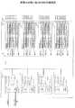
情報処理装置101は、プロセッサ201、メモリコントローラ301、およびHMC401を備える。情報処理装置101は、例えば、サーバやPC等のコンピュータである。 The
プロセッサ201は、HMC401に対するリクエストを発行する。プロセッサ201は、例えば、Central Processing Unit(CPU)である。 The
メモリコントローラ301は、プロセッサ201からリクエストを受信し、受信したリクエストを所定のルールに基づいて順番に、HMC401に送信する。 The
メモリコントローラ301は、FIFO311、リクエストコントローラ321、リクエストセレクタ331、リクエスト発行履歴レジスタ341、TOKENレジスタ351、Link MASTER361、Link Slave371を備える。 The
FIFO311は、プロセッサから発行されたリクエストが発行順に並んだリクエストキューを格納する。FIFO311は、例えば、シフトレジスタである。FIFO311は、フリップフロップ312−m(m=0〜7)を備える。FIFO311は、バッファの一例である。 The FIFO 311 stores a request queue in which requests issued from the processor are arranged in the order of issue. The FIFO 311 is, for example, a shift register. The FIFO 311 includes flip-flops 312-m (m = 0 to 7). The FIFO 311 is an example of a buffer.
フリップフロップ312−mは直列に接続されている。フリップフロップ312−mはリクエストを格納する。フリップフロップ312−2〜312−7は、それぞれ格納しているリクエストを後段のフリップフロップ312−0〜312−6に出力する。また、フリップフロップ312−mは、格納しているリクエストをリクエストセレクタ331に出力する。リクエストセレクタ331に出力される各リクエストには、リクエストキューのうちの何番目のリクエストであるかを示す情報(キュー番号)、すなわちどのフリップフロップ312−mに格納されているリクエストであるかを示す情報が含まれる。明細書及び図面において、フリップフロップ312−mに格納されているリクエストをそれぞれQmと表記する場合がある。 The flip-flops 312-m are connected in series. The flip-flop 312-m stores the request. The flip-flops 312-2 to 312-7 output the stored requests to the subsequent flip-flops 312-0 to 312-6. In addition, the flip-flop 312-m outputs the stored request to the
リクエストコントローラ321は、フリップフロップ312−mに格納されているリクエストへの読み書きやリクエストのシフトを制御する。リクエストコントローラ321は、リクエストセレクタ331から発行リクエストを受信し、発行リクエストに含まれているリクエストキューのうちのどのリクエストが選択されたかを示す情報(キュー番号)、すなわち選択されたリクエストを格納するフリップフロップ312−mを示す情報に基づいて、FIFO311に格納されているリクエストをシフトする。詳細には、リクエストコントローラ321は、選択されたリクエストより古いリクエストをホールドし、選択されたリクエストより新しいリクエストを1段シフトする。 The
リクエストセレクタ331は、リクエストキューに含まれる複数のリクエストから発行するリクエストを選択し、Link Master361に送信する。 The
リクエスト発行履歴レジスタ341は、リクエストセレクタ331が選択(出力)した新しい順に所定数のリクエストを格納する。詳細には、リクエスト発行履歴レジスタ341は、リクエストセレクタ331が選択した新しい順に所定数のリクエストのアドレスを格納する。 The request issuance history register 341 stores a predetermined number of requests in the new order selected (output) by the
TOKENレジスタ351は、メモリコントローラ301が送信可能なパケット数を格納する。メモリコントローラ301が送信可能なパケット数は、言い換えれば、HMC401が受け付け可能なパケット数である。TOKENレジスタ351は、送信したパケットのパケット数をLink MASTER361から受信し、送信可能なパケット数から送信したパケット数を減算する。TOKENレジスタ351は、Link Slave371からTokenパケットを受信し、送信可能なパケット数にTokenパケットが示すパケット数を加算する。 The TOKEN register 351 stores the number of packets that can be transmitted by the
Link MASTER361は、リクエストセレクタ331から受信したリクエストにヘッダやCRCを付加してパケットを生成し、HMC401に送信する。また、受信したリクエストに関連するパケットを生成し、HMC401に送信する。例えば、リクエストがデータの読み出しを要求するリードコマンドの場合、リードコマンドを含むパケットが生成及び送信される。例えば、リクエストがデータの書き込みを要求するライトコマンドであり且つ書き込みデータのサイズが大きい場合、書き込みデータは分割され、ライトコマンドと分割された書き込みデータの一部を含むパケット、および残りの分割された書き込みデータを含む複数のパケットが生成及び送信される。また、Link MASTER361は、送信したパケットの数(パケット数)をTOKENレジスタ351に通知する。 The link master 361 generates a packet by adding a header or CRC to the request received from the
Link Slave371は、HMC401からTokenパケットを受信し、TokenパケットをTokenレジスタ351に送信する。また、Link Slave371は、HMC401から読み出したデータを含む応答を受信し、プロセッサ201に送信する。 The
HMC401は、データを記憶する記憶装置である。HMC401は、受信したリクエストに応じてデータの読み書きを行う。 The
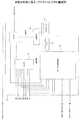
図2は、実施の形態に係るHMCの構成図である。
HMC401は、リンクインタフェースコントローラ411−i(i=1〜4)、スイッチ421、およびクアドラント(Quadrant)431−iを備える。FIG. 2 is a configuration diagram of the HMC according to the embodiment.
The
リンクインタフェースコントローラ411−iは、スイッチ421と接続し、クアドラント431−iと通信する場合、スイッチ421を介して通信する。 The link interface controller 411-i is connected to the
リンクインタフェースコントローラ411−iは、Link Slave412−i、入力バッファ413−i、およびLink Master414−iを備える。 The link interface controller 411-i includes a Link Slave 412-i, an input buffer 413-i, and a Link Master 414-i.
実施の形態では、複数のリンクインタフェースコントローラ411−iのうち、リンクインタフェースコントローラ411−1のみが使用され、リンクインタフェースコントローラ411−1はメモリコントローラ301と接続して通信する。尚、メモリコントローラ301と接続して通信するリンクインタフェースコントローラ411−iの数は、これに限られず、任意でよい。 In the embodiment, only the link interface controller 411-1 is used among the plurality of link interface controllers 411-i, and the link interface controller 411-1 is connected to and communicates with the
スイッチ421は、リンクインタフェースコントローラ411とクアドラント431とを接続する。スイッチ421を介することにより、任意のリンクインタフェースコントローラ411−iとクアドラント431−i間で通信を行うことができる。スイッチ421は、例えば、クロスバスイッチである。 The
クアドラント431−iは、Vault432−i−j(j=1〜4)を備える。クアドラント431−iは、リンクインタフェースコントローラ411−iに関連付けられたVault432−i−jの集合(グループ)である。実施の形態では、リンクインタフェースコントローラ411−1〜411−4それぞれに対し、関連付けられたクアドラント431−1〜431−4がある。リンクインタフェースコントローラ411−iに関連付けられたクアドラント431−iは、リンクインタフェースコントローラ411−iに直接属するクアドラント431−iと呼ぶ場合がある。リンクインタフェースコントローラ411−iは、直接属するクアドラント431−iに対し、直接には属しないクアドラント431−iよりも高速にアクセスできる。クアドラント431−iは、メモリグループの一例である。以下、Vault432−1−1〜433−4−4をそれぞれVault0〜15と表記する場合がある。 The quadrant 431-i includes a Vault 432-ij (j = 1 to 4). The quadrant 431-i is a set (group) of Vaults 432-i-j associated with the link interface controller 411-i. In the embodiment, there are quadrants 431-1 to 431-4 associated with each of the link interface controllers 411-1 to 411-4. The quadrant 431-i associated with the link interface controller 411-i may be referred to as a quadrant 431-i that directly belongs to the link interface controller 411-i. The link interface controller 411-i can access the quadrant 431-i to which it directly belongs at a higher speed than the quadrant 431-i that does not belong directly. Quadrant 431-i is an example of a memory group. Hereinafter, the Vaults 432-1-1 to 433-4-4 may be referred to as Vaults 0 to 15, respectively.
Vault432−i−jは、Vaultコントローラ433−i−jおよびメモリバンクグループ434−i−jを備える。Vault432−i−jには、それぞれアドレス(Vaultアドレス)が割り当てられる。Vault432−i−jは、メモリ部の一例である。 The Vault 432-ij includes a Vault controller 433-ij and a memory bank group 434-ij. An address (Vault address) is assigned to each of the Vault 432-ij. Vault 432-ij is an example of a memory unit.
Vaultコントローラ433−i−jは、メモリバンクグループ434−i−jを制御する。詳細には、Vaultコントローラ433−i−jは、メモリバンクグループ434−i−jに含まれるメモリバンクに対する読み書き等の制御を行う。 The vault controller 433-ij controls the memory bank group 434-ij. Specifically, the vault controller 433-ij performs control such as reading and writing with respect to the memory banks included in the memory bank group 434-ij.
メモリバンクグループ434−i−jは、メモリバンクの集合である。メモリバンクグループ434−i−jは、16個のメモリバンク0〜15を有する。 The memory bank group 434-ij is a set of memory banks. The memory bank group 434-ij has 16 memory banks 0-15.
図3は、実施の形態に係るリクエスト発行履歴レジスタの構成図である。
リクエスト発行履歴レジスタ341は、FIFO342、345、Vaultアドレスカウンタ344、およびBankアドレスカウンタ347を備える。FIG. 3 is a configuration diagram of a request issuance history register according to the embodiment.
The request
FIFO342は、リクエストセレクタ331が出力したリクエストに含まれるVault432−i−jのアドレス(以下、発行リクエストVaultアドレス)を新しい順に格納する。FIFO342は、フリップフロップ343−n(n=0〜14)を備える。すなわち、FIFO342は、15個の発行リクエストVaultアドレスを格納する。 The
フリップフロップ343−14には、リクエストセレクタ331が出力したリクエストが入力され、入力されたリクエストに含まれる発行リクエストVaultアドレスを格納する。リクエストセレクタ331からリクエストが出力されると、フリップフロップ343−1〜343−14は、それぞれ格納する発行リクエストVaultアドレスを後段のフリップフロップ343−0〜343−13に出力する。フリップフロップ343−0〜343−13は、前段のフリップフロップ343−1〜343−14から入力された発行リクエストVaultアドレスを格納する。このように、新しいリクエストがリクエストセレクタ331から発行されると、FIFO342内のデータ(発行リクエストVaultアドレス)はシフトし、FIFO342は、新しい順に15個の発行リクエストVaultアドレスを格納する。尚、フリップフロップ343−nの数は15に限られず、任意の数でよい。フリップフロップ343−nは、それぞれ格納する発行リクエストVaultアドレスをVaultアドレスカウンタ344に送信する。 The flip-flop 343-14 receives the request output from the
Vaultアドレスカウンタ344は、フリップフロップ343−nから入力された発行リクエストVaultアドレスを受信し、発行リクエストVaultアドレスが示すVault0〜15それぞれのアドレスの数をカウントする。Vaultアドレスカウンタ344は、カウントしたVault0〜15それぞれのアドレスの数をValult0〜15のリクエスト数としてリクエストセレクタ331に出力する。 The
FIFO345は、リクエストセレクタ331が発行したリクエストに含まれるメモリバンクのアドレス(以下、発行リクエストBankアドレス)を新しい順に格納する。FIFO345は、フリップフロップ346−n(n=0〜14)を備える。すなわち、FIFO342は、15個の発行リクエストBankアドレスを格納する。 The
フリップフロップ346−14には、リクエストセレクタ331が発行したリクエストが入力され、入力されたリクエストに含まれる発行リクエストBankアドレスを格納する。リクエストセレクタ331からリクエストが発行されると、フリップフロップ346−1〜346−14は、それぞれ格納する発行リクエストBankアドレスを後段のフリップフロップ346−0〜346−13に出力する。フリップフロップ346−0〜346−13は、前段のフリップフロップ343−1〜343−14から入力された発行リクエストBankアドレスを格納する。このように、新しいリクエストがリクエストセレクタ331から発行されると、FIFO345内のデータ(発行リクエストBankアドレス)はシフトし、FIFO345は、新しい順に15個の発行リクエストBankアドレスを格納する。尚、フリップフロップ346−nの数は15に限られず、任意の数でよい。フリップフロップ346−nは、それぞれ格納する発行リクエストBankアドレスをBankアドレスカウンタ347に送信する。 The flip-flop 346-14 receives a request issued by the
Bankアドレスカウンタ347は、フリップフロップ346−nから入力された発行リクエストBankアドレスを受信し、発行リクエストBankアドレスが示すメモリバンク0〜15それぞれのアドレスの数をカウントする。Bankアドレスカウンタ347は、カウントしたBank0〜15それぞれのアドレスの数をBank0〜15のリクエスト数としてリクエストセレクタ331に出力する。 The
図4は、実施の形態に係るリクエストセレクタの構成図である。
リクエストセレクタ331は、Tokenスレッシュホルドレジスタ332、比較回路333、リクエスト選択回路334、およびセレクタ335、336を備える。FIG. 4 is a configuration diagram of the request selector according to the embodiment.
The
Tokenスレッシュホルドレジスタ332は、閾値を格納する。尚、閾値は予め適当な値が設定されている。 The Token threshold register 332 stores a threshold value. Note that an appropriate value is set in advance as the threshold value.
比較回路333は、Tokenレジスタ351が格納する値(すなわち、メモリコントローラ301が送信可能なパケット数)とTokenスレッシュホルドレジスタ322が格納する閾値とを比較し、比較結果をセレクタ336に送信する。例えば、Tokenレジスタ351が格納する値が閾値以上の場合、比較結果はL(=0)、Tokenレジスタ351が格納する値が閾値未満の場合、比較結果はH(=1)とする。 The
リクエスト選択回路334は、各リクエストに含まれるVaultアドレスとBankアドレス、およびリクエスト履歴発行レジスタ341から入力されるValut0〜15のリクエスト数とBank0〜15のリクエスト数から、各リクエストQ0〜Q7の重みを算出する。実施の形態において、重みは9ビットで表現される。 The
各リクエストの重みは以下のように算出される。
リクエスト選択回路334は、リクエストが送信されるクアドラント431−iと同じクアドラント431−iに対して送信されたリクエストがリクエスト発行履歴レジスタ341に格納されたリクエストにあるか否か判定する。尚、リクエストがどのクアドラント431−iに送信されるかは、Vaultアドレスから判定できる。また、あるクアドラント431−iに対して送信されたリクエストがリクエスト発行履歴レジスタ341に格納されたリクエストにあるか否かは、Vault0〜15のリクエスト数から判定できる。例えば、Vault0のリクエスト数が1以上の場合、クアドラント431−1に対して送信されたリクエストがリクエスト発行履歴レジスタ341に格納されたリクエストにあると判定される。リクエストが送信されるクアドラント431−iと同じクアドラント431−iに対して送信されたリクエストがリクエスト発行履歴レジスタ341に格納されたリクエストにあった場合、リクエスト選択回路334は、重みの最上位ビットに1をセットする。無かった場合、リクエスト選択回路334は、重みの最上位ビットに0をセットする。重みの最上位ビットはリクエストが送信されるクアドラント431−iにコマンド発行履歴レジスタに格納されたリクエストが送信されていたか否かを示す。尚、他の実施の形態として、重みを12ビットにして、重みの上から1〜4ビット目(下から9〜12ビット目)に、リクエストが送信されるクアドラントにコマンド発行履歴レジスタに格納されたリクエストが送信された回数をセットしても良い。The weight of each request is calculated as follows.
The
リクエスト選択回路334は、リクエストのVaultアドレスと同じVaultのリクエスト数を重みの下から5〜8ビット目にセットする。重みの下から5〜8ビット目は、リクエストが送信されるVault432−i−jに対して、コマンド発行履歴レジスタに格納されたリクエストが送信された回数を示す。 The
リクエスト選択回路334は、リクエストのBankアドレスと同じBankのリクエスト数を重みの下から1〜4ビット目にセットする。 The
リクエスト選択回路334は、重みが1番小さいリクエストを選択する。これより、コマンド発行履歴レジスタに格納されたリクエストが送信された回数が最も少ない若しくは送信されていないクアドラントに送信するリクエストが選択される。リクエストが送信された回数が最も少ない若しくは送信されていないクアドラントに送信するリクエストが複数ある場合には、その中で、コマンド発行履歴レジスタに格納されたリクエストが送信された回数が最も少ないVault432−i−jに送信するリクエストが選択される。コマンド発行履歴レジスタに格納されたリクエストが送信された回数が最も少ないVault432−i−jに送信するリクエストが複数ある場合には、その中で、コマンド発行履歴レジスタに格納されたリクエストが送信された回数が最も少ないメモリバンクに送信するリクエストが選択される。 The
リクエスト選択回路334は、選択したリクエストを示す選択信号をセレクタ335に送信する。 The
また、上述の実施の形態では、重みにそれぞれ4ビットで示されるVaultのリクエスト数とBankのリクエスト数を用いていたが、それぞれ1ビットで示される同じVaultの有無および同じメモリバンクの有無を用いてもよい。それにより、回路規模を少なくすることが可能である。 In the above-described embodiment, the number of vault requests and the number of bank requests each indicated by 4 bits are used for the weight, but the presence or absence of the same vault and the presence or absence of the same memory bank each indicated by 1 bit are used. May be. Thereby, the circuit scale can be reduced.
セレクタ335には、リクエストQ0〜Q7と選択信号が入力される。セレクタ335は、入力された選択信号が示すリクエストを選択し、セレクタ336に出力する。 The
セレクタ336は、比較結果に基づいて、リクエストQ0またはセレクタ335から出力されたリクエストのいずれかを選択し、出力する。セレクタ336は、比較結果がLの場合(すなわち、Tokenレジスタ351が格納する値が閾値以上の場合)、リクエストQ0を選択し、出力する。セレクタ336は、比較結果がHの場合(すなわち、Tokenレジスタ351が格納する値が閾値未満の場合)、セレクタ335から出力されたリクエストを選択し、出力する。出力されたリクエストは、発行リクエストとも呼ぶ。 The selector 336 selects and outputs either the request Q0 or the request output from the
図5は、実施の形態に係るリクエスト選択処理のフローチャートである。
ステップS501において、比較回路333は、Tokenレジスタ351が格納する値(すなわち、メモリコントローラ301が送信可能なパケット数)とTokenスレッシュホルドレジスタ322が格納する閾値とを比較し、比較結果をセレクタ336に送信する。Tokenレジスタ351が格納する値が閾値以上の場合、制御はステップS502に進み、Tokenレジスタ351が格納する値が閾値未満の場合、制御はステップS503に進む。FIG. 5 is a flowchart of the request selection process according to the embodiment.
In step S501, the
ステップS502において、セレクタ336は、リクエストキューの先頭のリクエストQ0を選択し、Link Master361に出力する。 In step S502, the selector 336 selects the request Q0 at the head of the request queue and outputs it to the Link Master 361.
ステップS503において、リクエスト選択回路334は、リクエストQ0〜Q7のそれぞれの重みをリクエストQ0〜Q7のアドレスとVault0〜fのリクエスト履歴数とBank0〜fのリクエスト履歴数から算出する。 In step S503, the
ステップS504において、リクエスト選択回路334は、一番小さい重みに対応するリクエストを示す選択信号をセレクタ335に出力する。セレクタ335は、リクエストQ0〜Q7のうち、選択信号が示すリクエストを選択し、セレクタ336に出力する。 In step S504, the
ステップS505において、セレクタ336は、セレクタ335から入力されたリクエストを選択し、Link Master361に出力する。Link Master361は、入力されたリクエストを含むパケットを生成し、HMC401に送信する。 In step S505, the selector 336 selects the request input from the
図6は、実施の形態に係るメモリコントローラのタイミングチャートである。
サイクルC1において、FIFO311に格納されたリクエストキューのうちQ0〜Q5はそれぞれリクエストR0〜R5である。プロセッサ201からはリクエストR6が発行される。Tokenレジスタ351が格納する値が閾値以上であり、Tokenレジスタ351が格納する値が閾値以上であるか否かを示す比較結果はアサートされておらず、先頭のリクエストR0が選択され、出力される。FIG. 6 is a timing chart of the memory controller according to the embodiment.
In the cycle C1, Q0 to Q5 among the request queues stored in the
サイクルC2において、プロセッサ201からはリクエストR7が発行される。FIFO311に格納されたリクエストR0〜R5は1段シフトされる。それにより、リクエストR0は削除され、Q0〜Q5はそれぞれリクエストR1〜R4となる。また、リクエストR6は、リクエストキューの最後尾に格納されるので、Q5がリクエストR6となる。比較結果はアサートされておらず、先頭のリクエストR1が選択され、出力される。 In cycle C2, the
サイクルC3において、FIFO311に格納されたリクエストR1〜R6は1段シフトされる。それにより、リクエストR1は削除され、Q0〜Q5はそれぞれリクエストR2〜R6となる。また、リクエストR7は、リクエストキューの最後尾に格納されるので、Q5がリクエストR7となる。Tokenレジスタ351が格納する値が閾値未満となり、比較結果はアサートされる。リクエスト選択回路334により、Q3=リクエストR5が選択され、出力される。 In cycle C3, the requests R1 to R6 stored in the
サイクルC4において、FIFO311に格納されたリクエストR2〜R7のうち、サイクルC3で選択されたリクエストR5より前の(古い)リクエストR2〜R4はホールドされ、リクエストR5より後の(新しい)リクエストR6、R7は1段シフトされる。それにより、リクエストR1は削除され、Q0〜Q4はそれぞれリクエストR2〜R4、R6、R7となる。比較結果はアサートされている。リクエスト選択回路334により、Q3=リクエストR6が選択され、出力される。 In the cycle C4, among the requests R2 to R7 stored in the
サイクルC5において、プロセッサ201からはリクエストR8が発行される。FIFO311に格納されたリクエストR2〜R4、R6、R7のうち、サイクルC4で選択されたリクエストR6より前のリクエストR2〜R4はホールドされ、リクエストR6より後のリクエストR7は1段シフトされる。それにより、リクエストR6は削除され、Q0〜Q3はそれぞれリクエストR2〜R4、R7となる。Tokenレジスタ351が格納する値が閾値以上となり、比較結果はネゲートされ、先頭のリクエストR2が選択され、出力される。 In cycle C5, the
サイクルC6において、FIFO311に格納されたリクエストR2〜R4、R7は1段シフトされる。それにより、リクエストR2は削除され、Q0〜Q2はそれぞれリクエストR3、R4、R7となる。また、リクエストR8は、リクエストキューの最後尾に格納されるので、Q3がリクエストR8となる。比較結果はアサートされておらず、先頭のリクエストR3が選択され、出力される。 In cycle C6, the requests R2 to R4 and R7 stored in the
実施の形態の情報処理装置によれば、過去のリクエストのアドレス履歴に基づいて、送信された回数が少ないクアドラント、Vault、またはメモリバンクに対するリクエストを選択して送信することで、同一のクアドラント、同一のVault、または同一のメモリバンクへのアクセスが分散し、スループットの低下を防止することができる。 According to the information processing apparatus of the embodiment, by selecting and transmitting a request for a quadrant, a vault, or a memory bank with a small number of transmissions based on the address history of past requests, the same quadrant, the same Vault or accesses to the same memory bank are distributed, and a reduction in throughput can be prevented.
以上の実施の形態に関し、さらに以下の付記を開示する。
(付記1)
データを記憶する記憶装置と、
前記記憶装置に対するリクエストを発行する演算処理装置と、
前記演算処理装置が発行した未選択のリクエストである未選択リクエストを格納するバッファと、前記記憶装置に送信されたリクエストである送信済みリクエストのアドレスを保持する履歴レジスタと、前記履歴レジスタに保持された送信済みリクエストのアドレスに基づいて、前記記憶装置に送信する対象リクエストを前記バッファが格納する未選択リクエストから選択するとともに、選択された前記対象リクエストを前記記憶装置に送信する選択部とを備えたメモリ制御装置とを有する情報処理装置。
(付記2)
前記記憶装置は、前記メモリ制御装置と接続する複数のインタフェースコントローラ、および前記複数のインタフェースコントローラそれぞれに割り当てられた複数のメモリグループを備え、
前記メモリ制御装置は、前記送信済みリクエストが送信された回数が最も少ないメモリグループに送信するリクエストを前記未選択リクエストから選択することを特徴とする付記1記載の情報処理装置。
(付記3)
複数のメモリグループのそれぞれは、複数のメモリ部を備え、
前記複数のメモリ部のそれぞれは、制御部と前記制御部により制御される複数のメモリバンクを備え、
前記メモリ制御装置は、前記送信済みリクエストが送信された回数が最も少ないメモリ部に送信するリクエストを前記未選択リクエストから選択する付記2記載の情報処理装置。
(付記4)
前記メモリ制御装置は、前記送信済みリクエストが送信された回数が最も少ないメモリバンクに送信するリクエストを前記未選択リクエストから選択して送信する付記3記載の情報処理装置。
(付記5)
前記バッファは、前記未選択リクエストを前記演算処理装置から発行された順番に格納し、選択された前記対象リクエストより古いリクエストはホールドし、選択された前記対象リクエストより新しいリクエストをシフトすることを特徴とする付記1乃至4のいずれか1項に記載の情報処理装置。
(付記6)
演算処理装置が発行した未選択のリクエストである未選択リクエストを格納するバッファと、
記憶装置に送信されたリクエストである送信済みリクエストのアドレスを保持する履歴レジスタと、
前記履歴レジスタに保持された送信済みリクエストのアドレスに基づいて、前記記憶装置に送信する対象リクエストを前記バッファが格納する未選択リクエストから選択するとともに、選択された前記対象リクエストを記憶装置に送信する選択部と
を備えるメモリ制御装置。
(付記7)
前記記憶装置は、前記メモリ制御装置と接続する複数のインタフェースコントローラ、および前記複数のインタフェースコントローラそれぞれに割り当てられた複数のメモリグループを備え、
前記選択部は、前記送信済みリクエストが送信された回数が最も少ないメモリグループに送信するリクエストを前記未選択リクエストから選択することを特徴とする付記6記載のメモリ制御装置。
(付記8)
前記複数のメモリグループのそれぞれは、複数のメモリ部を備え、
前記複数のメモリ部のそれぞれは、制御部と前記制御部により制御される複数のメモリバンクを備え、
前記選択部は、前記送信済みリクエストが送信された回数が最も少ないメモリ部に送信するリクエストを前記未選択リクエストから選択する付記7記載のメモリ制御装置。
(付記9)
前記選択部は、前記送信済みリクエストが送信された回数が最も少ないメモリバンクに送信するリクエストを前記未選択リクエストから選択して送信する付記8記載のメモリ制御装置。
(付記10)
前記バッファは、前記未選択リクエストを前記演算処理装置から発行された順番に格納し、選択された前記対象リクエストより古いリクエストはホールドし、選択された前記対象リクエストより新しいリクエストをシフトすることを特徴とする付記6乃至9のいずれか1項に記載のメモリ制御装置。
(付記11)
データを記憶する記憶装置と、前記記憶装置に対するリクエストを発行する演算処理装置と、前記演算処理装置が発行した未選択のリクエストである未選択リクエストを格納するバッファと前記記憶装置に送信されたリクエストである送信済みリクエストのアドレスを保持する履歴レジスタとを備えたメモリ制御装置と、を有する情報処理装置の制御方法において、
前記メモリ制御装置が、前記履歴レジスタに保持された送信済みリクエストのアドレスに基づいて、前記記憶装置に送信する対象リクエストを前記バッファが格納するリクエストから選択し、
前記メモリ制御装置が、選択された前記対象リクエストを前記記憶装置に送信する情報処理装置の制御方法。
(付記12)
前記記憶装置は、前記メモリ制御装置と接続する複数のインタフェースコントローラ、および前記複数のインタフェースコントローラそれぞれに割り当てられた複数のメモリグループを備え、
前記選択する処理は、前記送信済みリクエストが送信された回数が最も少ないメモリグループに送信するリクエストを前記未選択リクエストから選択することを特徴とする付記11記載の制御方法。
(付記13)
前記複数のメモリグループのそれぞれは、複数のメモリ部を備え、
前記複数のメモリ部のそれぞれは、制御部と前記制御部により制御される複数のメモリバンクを備え、
前記選択する処理は、前記送信済みリクエストが送信された回数が最も少ないメモリ部に送信するリクエストを前記未選択リクエストから選択する付記12記載の制御方法。
(付記14)
前記選択する処理は、前記送信済みリクエストが送信された回数が最も少ないメモリバンクに送信するリクエストを前記未選択リクエストから選択して送信する付記13記載の制御方法。
(付記15)
前記バッファは、前記未選択リクエストを前記演算処理装置から発行された順番に格納し、
選択された前記対象リクエストより古いリクエストはホールドし、選択された前記対象リクエストより新しいリクエストをシフトする処理をさらに備えることを特徴とする付記11乃至14のいずれか1項に記載の制御方法。Regarding the above embodiment, the following additional notes are disclosed.
(Appendix 1)
A storage device for storing data;
An arithmetic processing unit that issues a request to the storage device;
A buffer that stores an unselected request that is an unselected request issued by the arithmetic processing unit, a history register that holds an address of a transmitted request that is a request sent to the storage device, and a history register that holds A selection unit configured to select a target request to be transmitted to the storage device from unselected requests stored in the buffer based on the address of the transmitted request, and to transmit the selected target request to the storage device. An information processing device having a memory control device.
(Appendix 2)
The storage device includes a plurality of interface controllers connected to the memory control device, and a plurality of memory groups assigned to the plurality of interface controllers,
The information processing apparatus according to
(Appendix 3)
Each of the plurality of memory groups includes a plurality of memory units,
Each of the plurality of memory units includes a control unit and a plurality of memory banks controlled by the control unit,
The information processing device according to
(Appendix 4)
The information processing apparatus according to
(Appendix 5)
The buffer stores the unselected requests in an order issued from the arithmetic processing unit, holds a request older than the selected target request, and shifts a request newer than the selected target request. The information processing apparatus according to any one of
(Appendix 6)
A buffer for storing an unselected request that is an unselected request issued by the arithmetic processing unit;
A history register that holds the address of a sent request that is a request sent to the storage device;
Based on the address of the transmitted request held in the history register, the target request to be transmitted to the storage device is selected from the unselected requests stored in the buffer, and the selected target request is transmitted to the storage device. A memory control device comprising: a selection unit;
(Appendix 7)
The storage device includes a plurality of interface controllers connected to the memory control device, and a plurality of memory groups assigned to the plurality of interface controllers,
The memory control device according to appendix 6, wherein the selection unit selects, from the unselected requests, a request to be transmitted to a memory group having the least number of times the transmitted request has been transmitted.
(Appendix 8)
Each of the plurality of memory groups includes a plurality of memory units,
Each of the plurality of memory units includes a control unit and a plurality of memory banks controlled by the control unit,
The memory control device according to appendix 7, wherein the selection unit selects, from the unselected requests, a request to be transmitted to the memory unit with the least number of times the transmitted request has been transmitted.
(Appendix 9)
The memory control device according to appendix 8, wherein the selection unit selects and transmits a request to be transmitted to a memory bank having the least number of times the transmitted request has been transmitted from the unselected requests.
(Appendix 10)
The buffer stores the unselected requests in an order issued from the arithmetic processing unit, holds a request older than the selected target request, and shifts a request newer than the selected target request. 10. The memory control device according to any one of appendices 6 to 9.
(Appendix 11)
A storage device for storing data, an arithmetic processing device for issuing a request to the storage device, a buffer for storing an unselected request that is an unselected request issued by the arithmetic processing device, and a request transmitted to the storage device And a memory control device having a history register that holds an address of a transmitted request that is an information processing device control method,
Based on the address of the transmitted request held in the history register, the memory control device selects a target request to be transmitted to the storage device from requests stored in the buffer,
A method for controlling an information processing device, wherein the memory control device transmits the selected target request to the storage device.
(Appendix 12)
The storage device includes a plurality of interface controllers connected to the memory control device, and a plurality of memory groups assigned to the plurality of interface controllers,
The control method according to appendix 11, wherein the selecting process selects a request to be transmitted to a memory group having the smallest number of times the transmitted request has been transmitted from the unselected requests.
(Appendix 13)
Each of the plurality of memory groups includes a plurality of memory units,
Each of the plurality of memory units includes a control unit and a plurality of memory banks controlled by the control unit,
The control method according to
(Appendix 14)
The control method according to
(Appendix 15)
The buffer stores the unselected requests in the order issued from the arithmetic processing unit,
The control method according to any one of appendices 11 to 14, further comprising a process of holding a request older than the selected target request and shifting a request newer than the selected target request.
101 情報処理装置
201 プロセッサ
301 メモリコントローラ
311 FIFO
321 リクエストコントローラ
331 リクエストセレクタ
332 Tokenスレッシュホルドレジスタ
333 比較回路
334 リクエスト選択回路
335、336 セレクタ
341 リクエスト発行履歴レジスタ
342 FIFO
344 Vaultアドレスカウンタ
345 FIFO
347 Bankアドレスカウンタ
351 TOKENレジスタ
361 Link MASTER
371 Link Slave
401 HMC
411 リンクインタフェースコントローラ
412 Link Slave
413 入力バッファ
414 Link Master
421 スイッチ
431 クアドラント
432 Vault
433 Vaultコントローラ
434 メモリバンクグループ101
321
344
347
371 Link Slave
401 HMC
411 Link interface controller 412 Link Slave
413
421
433
Claims (7)
Translated fromJapanese前記記憶装置に対するリクエストを発行する演算処理装置と、
前記演算処理装置が発行した未選択のリクエストである未選択リクエストを格納するバッファと、前記記憶装置に送信されたリクエストである送信済みリクエストのアドレスを保持する履歴レジスタと、前記履歴レジスタに保持された送信済みリクエストのアドレスに基づいて、前記記憶装置に送信する対象リクエストとして、前記送信済みリクエストが送信された回数が最も少ないメモリグループに送信するリクエストを、前記バッファが格納する未選択リクエストから選択するとともに、選択された前記対象リクエストを前記記憶装置に送信する選択部とを備えたメモリ制御装置とを有する情報処理装置。A storage devicehaving a plurality of memory groups which are groups of memories for storing data;
An arithmetic processing unit that issues a request to the storage device;
A buffer that stores an unselected request that is an unselected request issued by the arithmetic processing unit, a history register that holds an address of a transmitted request that is a request sent to the storage device, and a history register that holds was based on the address of the transmitted request selectedas target request to be transmitted to the storagedevice, therequest number of times the sent request is transmitted to transmit the least memorygroup, from unselected request said buffer store And a memory control device including a selection unit that transmits the selected target request to the storage device.
前記複数のメモリ部のそれぞれは、制御部と前記制御部により制御される複数のメモリバンクを備え、
前記メモリ制御装置は、前記送信済みリクエストが送信された回数が最も少ないメモリ部に送信するリクエストを前記未選択リクエストから選択する請求項2記載の情報処理装置。Each of the plurality of memory groups includes a plurality of memory units,
Each of the plurality of memory units includes a control unit and a plurality of memory banks controlled by the control unit,
The information processing apparatus according to claim 2, wherein the memory control apparatus selects, from the unselected requests, a request to be transmitted to a memory unit having the least number of times the transmitted request has been transmitted.
データを記憶するメモリのグループであるメモリグループを複数有する記憶装置に送信されたリクエストである送信済みリクエストのアドレスを保持する履歴レジスタと、
前記履歴レジスタに保持された送信済みリクエストのアドレスに基づいて、前記記憶装置に送信する対象リクエストとして、前記送信済みリクエストが送信された回数が最も少ないメモリグループに送信するリクエストを、前記バッファが格納する未選択リクエストから選択するとともに、選択された前記対象リクエストを記憶装置に送信する選択部と
を備えるメモリ制御装置。A buffer for storing an unselected request that is an unselected request issued by the arithmetic processing unit;
A history register that holds an address of a transmitted request that is a request transmitted toa storage devicehaving a plurality of memory groups that are groups of memories that store data ;
Based on the address of the transmitted request held in the history register,a target request to be transmitted to the storagedevice, therequest number of times the sent request is transmitted to transmit the least memorygroup, said buffer storage A memory control device comprising: a selection unit that selects from the unselected requests to be transmitted and transmits the selected target request to a storage device.
前記メモリ制御装置が、前記履歴レジスタに保持された送信済みリクエストのアドレスに基づいて、前記記憶装置に送信する対象リクエストとして、前記送信済みリクエストが送信された回数が最も少ないメモリグループに送信するリクエストを、前記バッファが格納する未選択リクエストから選択し、
前記メモリ制御装置が、選択された前記対象リクエストを前記記憶装置に送信する情報処理装置の制御方法。A storage devicehaving a plurality of memory groups that are groups of memories for storing data, an arithmetic processing device that issues a request for the storage device, and an unselected request that is an unselected request issued by the arithmetic processing device In a control method for an information processing device, comprising: a memory control device including a buffer and a history register that holds an address of a transmitted request that is a request transmitted to the storage device;
Based on the address of the transmitted request held in the history register, the memory control devicetransmits a request to the memory group with the least number of times the transmitted request has been transmitted as a target request to be transmitted to the storage device.to highlight theunselected request said buffer store,
A method for controlling an information processing device, wherein the memory control device transmits the selected target request to the storage device.
Priority Applications (2)
| Application Number | Priority Date | Filing Date | Title |
|---|---|---|---|
| JP2015101267AJP6477228B2 (en) | 2015-05-18 | 2015-05-18 | Information processing apparatus, memory control apparatus, and information processing apparatus control method |
| US15/095,203US10078602B2 (en) | 2015-05-18 | 2016-04-11 | Information processing apparatus, memory controller, and memory control method |
Applications Claiming Priority (1)
| Application Number | Priority Date | Filing Date | Title |
|---|---|---|---|
| JP2015101267AJP6477228B2 (en) | 2015-05-18 | 2015-05-18 | Information processing apparatus, memory control apparatus, and information processing apparatus control method |
Publications (2)
| Publication Number | Publication Date |
|---|---|
| JP2016218635A JP2016218635A (en) | 2016-12-22 |
| JP6477228B2true JP6477228B2 (en) | 2019-03-06 |
Family
ID=57324785
Family Applications (1)
| Application Number | Title | Priority Date | Filing Date |
|---|---|---|---|
| JP2015101267AExpired - Fee RelatedJP6477228B2 (en) | 2015-05-18 | 2015-05-18 | Information processing apparatus, memory control apparatus, and information processing apparatus control method |
Country Status (2)
| Country | Link |
|---|---|
| US (1) | US10078602B2 (en) |
| JP (1) | JP6477228B2 (en) |
Families Citing this family (5)
| Publication number | Priority date | Publication date | Assignee | Title |
|---|---|---|---|---|
| US10157023B2 (en)* | 2016-02-25 | 2018-12-18 | SK Hynix Inc. | Memory controller and request scheduling method using request queues and first and second tokens |
| US10162781B2 (en)* | 2016-06-01 | 2018-12-25 | Micron Technology, Inc. | Logic component switch |
| DE102020106357A1 (en) | 2019-03-11 | 2020-09-17 | Samsung Electronics Co., Ltd. | STORAGE DEVICE AND INSTRUCTION RING STORAGE QUEUE PROCEDURE |
| CN110890120B (en)* | 2019-10-21 | 2021-08-31 | 中国科学院计算技术研究所 | A general block chain application processing acceleration method and system based on resistive memory |
| JP7476676B2 (en) | 2020-06-04 | 2024-05-01 | 富士通株式会社 | Processing Unit |
Family Cites Families (11)
| Publication number | Priority date | Publication date | Assignee | Title |
|---|---|---|---|---|
| JPH09198300A (en) | 1996-01-16 | 1997-07-31 | Hitachi Ltd | Memory access control method |
| US7538694B2 (en)* | 1999-01-29 | 2009-05-26 | Mossman Holdings Llc | Network device with improved storage density and access speed using compression techniques |
| US6836831B2 (en)* | 2002-08-08 | 2004-12-28 | International Business Machines Corporation | Independent sequencers in a DRAM control structure |
| US20080177994A1 (en)* | 2003-01-12 | 2008-07-24 | Yaron Mayer | System and method for improving the efficiency, comfort, and/or reliability in Operating Systems, such as for example Windows |
| JP2006215799A (en) | 2005-02-03 | 2006-08-17 | Toshiba Corp | Memory controller |
| US7522468B2 (en)* | 2006-06-08 | 2009-04-21 | Unity Semiconductor Corporation | Serial memory interface |
| US7660952B2 (en)* | 2007-03-01 | 2010-02-09 | International Business Machines Corporation | Data bus bandwidth scheduling in an FBDIMM memory system operating in variable latency mode |
| US7975109B2 (en)* | 2007-05-30 | 2011-07-05 | Schooner Information Technology, Inc. | System including a fine-grained memory and a less-fine-grained memory |
| US7978721B2 (en)* | 2008-07-02 | 2011-07-12 | Micron Technology Inc. | Multi-serial interface stacked-die memory architecture |
| WO2013095639A1 (en)* | 2011-12-23 | 2013-06-27 | Intel Corporation | Utility and lifetime based cache replacement policy |
| JP2014154119A (en)* | 2013-02-14 | 2014-08-25 | Ricoh Co Ltd | Memory controller and semiconductor storage device |
- 2015
- 2015-05-18JPJP2015101267Apatent/JP6477228B2/ennot_activeExpired - Fee Related
- 2016
- 2016-04-11USUS15/095,203patent/US10078602B2/enactiveActive
Also Published As
| Publication number | Publication date |
|---|---|
| US10078602B2 (en) | 2018-09-18 |
| JP2016218635A (en) | 2016-12-22 |
| US20160342541A1 (en) | 2016-11-24 |
Similar Documents
| Publication | Publication Date | Title |
|---|---|---|
| US10642612B2 (en) | Memory device performing parallel arithmetic processing and memory module including the same | |
| JP6477228B2 (en) | Information processing apparatus, memory control apparatus, and information processing apparatus control method | |
| CN110175140A (en) | Fusion memory part and its operating method | |
| US10152434B2 (en) | Efficient arbitration for memory accesses | |
| EP1754229A2 (en) | System and method for improving performance in computer memory systems supporting multiple memory access latencies | |
| US11853231B2 (en) | Transmission of address translation type packets | |
| US12254213B2 (en) | Write request buffer capable of responding to read requests | |
| US12039200B2 (en) | Load balancing between storage devices | |
| CN111399757A (en) | Memory system and operating method thereof | |
| CN111209227B (en) | data processing system | |
| JP6331944B2 (en) | Information processing apparatus, memory control apparatus, and information processing apparatus control method | |
| US10684965B2 (en) | Method to reduce write responses to improve bandwidth and efficiency | |
| JP2011013835A (en) | Memory system, memory access method and program | |
| US10936534B2 (en) | Converged memory device and method thereof | |
| US11734203B2 (en) | Response-based interconnect control | |
| EP3244582B1 (en) | Switch and data accessing method thereof | |
| US12321288B2 (en) | Asymmetric read-write sequence for interconnected dies | |
| US12236098B2 (en) | Memory device and scheduling method thereof | |
| EP4586141A1 (en) | Smart storage devices | |
| EP4394576A1 (en) | Apparatus and methods for accessing data at a storage node | |
| US10216454B1 (en) | Method and apparatus of performing a memory operation in a hierarchical memory assembly | |
| KR20190056626A (en) | Convergence memory device and method thereof | |
| CN116578501A (en) | Memory address allocation and cache mapping for retaining data in cache |
Legal Events
| Date | Code | Title | Description |
|---|---|---|---|
| A621 | Written request for application examination | Free format text:JAPANESE INTERMEDIATE CODE: A621 Effective date:20180206 | |
| A977 | Report on retrieval | Free format text:JAPANESE INTERMEDIATE CODE: A971007 Effective date:20181127 | |
| A131 | Notification of reasons for refusal | Free format text:JAPANESE INTERMEDIATE CODE: A131 Effective date:20181204 | |
| A521 | Request for written amendment filed | Free format text:JAPANESE INTERMEDIATE CODE: A523 Effective date:20181220 | |
| TRDD | Decision of grant or rejection written | ||
| A01 | Written decision to grant a patent or to grant a registration (utility model) | Free format text:JAPANESE INTERMEDIATE CODE: A01 Effective date:20190108 | |
| A61 | First payment of annual fees (during grant procedure) | Free format text:JAPANESE INTERMEDIATE CODE: A61 Effective date:20190121 | |
| R150 | Certificate of patent or registration of utility model | Ref document number:6477228 Country of ref document:JP Free format text:JAPANESE INTERMEDIATE CODE: R150 | |
| LAPS | Cancellation because of no payment of annual fees |