JP6473578B2 - Optical connector - Google Patents
Optical connectorDownload PDFInfo
- Publication number
- JP6473578B2 JP6473578B2JP2014116622AJP2014116622AJP6473578B2JP 6473578 B2JP6473578 B2JP 6473578B2JP 2014116622 AJP2014116622 AJP 2014116622AJP 2014116622 AJP2014116622 AJP 2014116622AJP 6473578 B2JP6473578 B2JP 6473578B2
- Authority
- JP
- Japan
- Prior art keywords
- optical
- connector
- housing
- connector housing
- case
- Prior art date
- Legal status (The legal status is an assumption and is not a legal conclusion. Google has not performed a legal analysis and makes no representation as to the accuracy of the status listed.)
- Active
Links
- 230000003287optical effectEffects0.000titleclaimsdescription82
- 230000013011matingEffects0.000claimsdescription5
- 238000003780insertionMethods0.000description5
- 230000037431insertionEffects0.000description5
- 239000000758substrateSubstances0.000description5
- 230000004308accommodationEffects0.000description3
- 230000005540biological transmissionEffects0.000description3
- 239000013307optical fiberSubstances0.000description3
- 230000000052comparative effectEffects0.000description2
- ORQBXQOJMQIAOY-UHFFFAOYSA-NnobeliumChemical compound[No]ORQBXQOJMQIAOY-UHFFFAOYSA-N0.000description2
- 239000000853adhesiveSubstances0.000description1
- 230000001070adhesive effectEffects0.000description1
- 239000000835fiberSubstances0.000description1
- 238000000034methodMethods0.000description1
Images


Classifications
- G—PHYSICS
- G02—OPTICS
- G02B—OPTICAL ELEMENTS, SYSTEMS OR APPARATUS
- G02B6/00—Light guides; Structural details of arrangements comprising light guides and other optical elements, e.g. couplings
- G02B6/24—Coupling light guides
- G02B6/42—Coupling light guides with opto-electronic elements
- G02B6/4201—Packages, e.g. shape, construction, internal or external details
- G02B6/4219—Mechanical fixtures for holding or positioning the elements relative to each other in the couplings; Alignment methods for the elements, e.g. measuring or observing methods especially used therefor
- G02B6/4234—Passive alignment along the optical axis and active alignment perpendicular to the optical axis
- G—PHYSICS
- G02—OPTICS
- G02B—OPTICAL ELEMENTS, SYSTEMS OR APPARATUS
- G02B6/00—Light guides; Structural details of arrangements comprising light guides and other optical elements, e.g. couplings
- G02B6/24—Coupling light guides
- G02B6/42—Coupling light guides with opto-electronic elements
- G02B6/4201—Packages, e.g. shape, construction, internal or external details
- G02B6/4246—Bidirectionally operating package structures
- G—PHYSICS
- G02—OPTICS
- G02B—OPTICAL ELEMENTS, SYSTEMS OR APPARATUS
- G02B6/00—Light guides; Structural details of arrangements comprising light guides and other optical elements, e.g. couplings
- G02B6/24—Coupling light guides
- G02B6/42—Coupling light guides with opto-electronic elements
- G02B6/4201—Packages, e.g. shape, construction, internal or external details
- G02B6/4204—Packages, e.g. shape, construction, internal or external details the coupling comprising intermediate optical elements, e.g. lenses, holograms
- G—PHYSICS
- G02—OPTICS
- G02B—OPTICAL ELEMENTS, SYSTEMS OR APPARATUS
- G02B6/00—Light guides; Structural details of arrangements comprising light guides and other optical elements, e.g. couplings
- G02B6/24—Coupling light guides
- G02B6/42—Coupling light guides with opto-electronic elements
- G02B6/4201—Packages, e.g. shape, construction, internal or external details
- G02B6/4219—Mechanical fixtures for holding or positioning the elements relative to each other in the couplings; Alignment methods for the elements, e.g. measuring or observing methods especially used therefor
- G02B6/4236—Fixing or mounting methods of the aligned elements
- G02B6/4245—Mounting of the opto-electronic elements
- G—PHYSICS
- G02—OPTICS
- G02B—OPTICAL ELEMENTS, SYSTEMS OR APPARATUS
- G02B6/00—Light guides; Structural details of arrangements comprising light guides and other optical elements, e.g. couplings
- G02B6/24—Coupling light guides
- G02B6/42—Coupling light guides with opto-electronic elements
- G02B6/4201—Packages, e.g. shape, construction, internal or external details
- G02B6/4256—Details of housings
- G02B6/426—Details of housings mounting, engaging or coupling of the package to a board, a frame or a panel
- G—PHYSICS
- G02—OPTICS
- G02B—OPTICAL ELEMENTS, SYSTEMS OR APPARATUS
- G02B6/00—Light guides; Structural details of arrangements comprising light guides and other optical elements, e.g. couplings
- G02B6/24—Coupling light guides
- G02B6/42—Coupling light guides with opto-electronic elements
- G02B6/4292—Coupling light guides with opto-electronic elements the light guide being disconnectable from the opto-electronic element, e.g. mutually self aligning arrangements
Landscapes
- Physics & Mathematics (AREA)
- General Physics & Mathematics (AREA)
- Optics & Photonics (AREA)
- Optical Couplings Of Light Guides (AREA)
- Light Receiving Elements (AREA)
Description
Translated fromJapanese本発明は、相手側フェルールとの間で光伝送を行う光トランシーバを備えた光コネクタに関する。 The present invention relates to an optical connector including an optical transceiver that performs optical transmission with a counterpart ferrule.
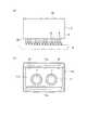
図5及び図6には、光コネクタの従来例が示されている(特許文献1参照)。図5及び図6に示すように、光コネクタ100は、光トランシーバ(FOT: Fiber・Optical・Transceiver)101と、光トランシーバ101を収容するコネクタハウジング110とを備えている。光トランシーバ101は、相手側フェルール(図示せず)との間で光伝送する光素子102と、光素子102を覆うケース103と、ケース103の端子突出面103aより外部に突出された複数の端子104とを有する。コネクタハウジング110の後端側(図5(b)の右側)には、光トランシーバ101を収容する収容室111が形成されている。収容室111には、1面(図5(b)の下面)111aが開口され、光トランシーバ101の3面に当接する面が形成されている。コネクタハウジング110の前端側(図5(b)の左側)には、光ファイバ120の端部が挿入されるフェルールガイド部112が形成されている。 5 and 6 show a conventional example of an optical connector (see Patent Document 1). As shown in FIGS. 5 and 6, the
上記構成にあって、コネクタハウジング110内の収容室111の開口された1面(図5(b)の下面)111aより光トランシーバ101を挿入する。これにより、光トランシーバ101の3面がコネクタハウジング110内の収容室111に形成される各面に当接するので、光トランシーバ101がコネクタハウジング110に位置決めされる。その結果、光トランシーバ101の光軸は、光ファイバ120の光軸C1と一致し、光ファイバ120と光トランシーバ101間の光伝達を円滑に行うことができる。 In the above configuration, the
ところで、前記従来例にあっては、光トランシーバ101をコネクタハウジング110内の収容室111に挿入可能にするため、収容室111の幅寸法W1を光トランシーバ101の横幅(側面間の寸法)W2より少し大きな寸法にする必要がある。しかしながら、このように収容室111の幅寸法W1が光トランシーバ101の横幅W2より大きいと、この寸法差(W1−W2)によって収容された光トランシーバ101が回転方向に位置ずれする。 By the way, in the conventional example, in order to allow the
そこで、本発明は、前記した課題を解決すべくなされたものであり、光トランシーバのコネクタハウジングに対する回転方向の位置ずれを極力防止できる光コネクタを提供することを目的とする。 Accordingly, the present invention has been made to solve the above-described problems, and an object of the present invention is to provide an optical connector that can prevent the positional deviation of the optical transceiver relative to the connector housing in the rotational direction as much as possible.
本発明は、光素子と前記光素子を覆うケースと前記ケースの端子突出面より外部に突出された複数の端子とを有する光トランシーバと、前記光トランシーバを収容する収容室を有するコネクタハウジングとを備えた光コネクタであって、前記ケースの前記端子突出面は、平坦な基準面として形成され、前記コネクタハウジングの前記収容室を形成する面で、且つ、前記ケースの前記端子突出面が当接する面は、平坦な位置矯正面として形成され、前記コネクタハウジングの前記収容室を形成する面で、且つ、前記ケースの前記端子突出面が当接する面の対向面には、突起が設けられ、複数の前記端子は、前記端子突出面の長手方向に沿って間隔を置いて配置され、前記コネクタハウジングが搭載基板上に載置された状態では、複数の前記端子の先端部が前記搭載基板に面接触して表面実装されることを特徴とする光コネクタである。The present invention includes an optical transceiver having an optical element, a case that covers the optical element, and a plurality of terminals that protrude outward from a terminal protruding surface of the case, and a connector housing that has a storage chamber for storing the optical transceiver. The terminal projecting surface of the case is formed as a flat reference surface, is a surface that forms the housing chamber of the connector housing, and the terminal projecting surface of the case is in contact with the optical connector. The surface is formed as a flat position correction surface, is a surface that forms thehousing chamber of the connector housing, and a protrusion is provided on a surface opposite to the surface with which the terminal protruding surface of the case abuts. The terminals are arranged at intervals along the longitudinal direction of the terminal protruding surface, and in a state where the connector housing is placed on a mounting board, a plurality of the terminals are provided. An optical connector, wherein the tip is surface-mounted in surface contact with the mounting substrate.
前記コネクタハウジングの前記収容室は、相手側コネクタハウジングが装着される側の反対側の面が開口され、前記光トランシーバが前記開口より前記収容室に挿入されることが好ましい。 In the housing of the connector housing, it is preferable that a surface opposite to the side on which the mating connector housing is mounted is opened, and the optical transceiver is inserted into the housing through the opening.
本発明によれば、コネクタハウジングの収容室に光トランシーバを挿入すると、コネクタハウジングの収容室に設けられた突起の復帰変形力によってケースの端子突出面がコネクタハウジングの位置矯正面に押圧されるため、光トランシーバがコネクタハウジングに位置決めされた状態で収容される。これにより、光トランシーバのコネクタハウジングに対する回転方向の位置ずれを極力防止できる。 According to the present invention, when the optical transceiver is inserted into the housing of the connector housing, the terminal projecting surface of the case is pressed against the position correcting surface of the connector housing by the restoring deformation force of the protrusion provided in the housing of the connector housing. The optical transceiver is accommodated in a state of being positioned in the connector housing. Thereby, the position shift of the rotation direction with respect to the connector housing of an optical transceiver is prevented as much as possible.
以下、本発明の実施形態を図面に基づいて説明する。 Hereinafter, embodiments of the present invention will be described with reference to the drawings.
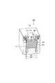
図1〜図4は本発明の一実施形態を示す。図1〜図4に示すように、光コネクタ1は、光トランシーバ2と、光トランシーバ2を収容するコネクタハウジング10と、コネクタハウジング10の外周を覆うシールドケース15とを備えている。 1 to 4 show an embodiment of the present invention. As shown in FIGS. 1 to 4, the optical connector 1 includes an
光トランシーバ2は、相手側フェルール(図示せず)が挿入されるフェルール挿入孔3aを有するスリーブ3と、リードフレーム(図示せず)に搭載され、相手側フェルールとの間で光伝送する光素子(図示せず)と、この光素子を覆うケース4と、ケース4の端子突出面4aより外部に突出された複数の端子6と、相手側フェルールとケース4間の光経路上に配置される球体状のレンズ7とを備えている。 The
各スリーブ3は、円筒状に形成され、内部のフェルール挿入孔3aにレンズ7が固定される。各スリーブ3は、軸心方向に延びるスリット3bを有している。 Each
複数の端子6は、ケース4内に埋設されるリードフレーム(図示せず)より延設されている。各端子6は、端子突出面4aの長手方向に沿って間隔を置いて配置されている。各端子6は、コネクタハウジング10が搭載基板8上に載置された状態では、各端子6の先端部が搭載基板8に面接触して表面実装されている。 The plurality of
コネクタハウジング10内の前端側(図2(a)の左側)には、前方から相手側コネクタハウジング(図示せず)が装着される。コネクタハウジング10の収容室11は、相手側コネクタハウジングが装着される側の反対側(図2(a)の右側)の面が開口され、この開口11aより光トランシーバ2が収容室11に挿入される。 A mating connector housing (not shown) is attached to the front end side (left side of FIG. 2A) in the connector housing 10 from the front. The
ケース4の端子突出面4aは、平坦な基準面として形成されている。コネクタハウジング10の収容室11の底面は、収容室11を形成する面で、且つ、ケース4の端子突出面4aが当接する面であり、平坦な位置矯正面11bとして形成されている。コネクタハウジング10の収容室11の天井面11cは、収容室11を形成する面で、且つ、ケース4の端子突出面4aが当接する面の対向面である。天井面11cには、幅方向の左右対称位置で、且つ、光トランシーバ2の挿入方向に延びる一対の突起12が設けられている。 The terminal protruding
次に、光トランシーバ2の組み立て手順を説明する。先ず、各スリーブ3のフェルール挿入孔3aの先端側にダミーフェルール(図示せず)を挿入し、スリット3bを利用してスリーブ3を縮径することによりダミーフェルールの外周に密着させる。これにより、ダミーフェルールの中心軸と同軸のスリーブ3が作製される。このスリーブ3のフェルール挿入孔3aの後端側に、ダミーフェルールと同一な直径のレンズ7を挿入して接着剤などで固定すると、レンズ7の中心軸とスリーブ3の中心軸が一致するレンズ7付きスリーブ3が作製される。 Next, the assembly procedure of the
次に、レンズ7付きスリーブ3及びケース4の組み付け品をコネクタハウジング10にセットする。その際、コネクタハウジング10の収容室11に後側の開口11aより光トランシーバ2を収容室11に挿入し、収容室11の天井面11cに設けられた一対の突起12をケース4の上面4bに当接させると共に、ケース4の端子突出面4aを収容室11の位置矯正面11bに当接させる。これにより、一対の突起12が圧縮変形するので、その復帰変形力によってケース4の端子突出面4aがコネクタハウジング10の収容室11の位置矯正面11bに押圧される。 Next, the assembly product of the
このようにして当該光コネクタ1を組み立てた後、コネクタハウジング10を搭載基板8上に載置し、ケース4の端子突出面4aから突出する複数の端子6の先端部が搭載基板8に面接触した状態で、当該光コネクタ1を表面実装する。 After assembling the optical connector 1 in this way, the
以上説明したように、光コネクタ1では、コネクタハウジング10の収容室11の天井面11cに設けられた一対の突起12の復帰変形力によってケース4の端子突出面4aがコネクタハウジング10の収容室11の位置矯正面11bに押圧される。従って、光トランシーバ2がコネクタハウジング10に位置決めされた状態で収容されるため、光トランシーバ2のコネクタハウジング10に対する回転方向の位置ずれを極力防止できる。 As described above, in the optical connector 1, the
上記したように、光トランシーバ2のコネクタハウジング10に対する回転方向の位置ずれを極力防止できるため、複数の端子4の底面が同一面上に位置し、光コネクタ1の搭載基板8における実装精度が向上する。 As described above, since the positional shift in the rotation direction of the
コネクタハウジング10の収容室11は、相手側コネクタハウジングが装着される側の反対側の面が開口され、この開口11aより光トランシーバ2が収容室11に挿入されるので、一対の突起12を圧縮変形させつつ光トランシーバ2を収容室11に挿入すれば良いため、光トランシーバ2の収容作業が容易である。 The
この実施形態では、ケース4の前記端子突出面4aが当接する面の対向面11cには、左右一対の突起12が設けられているが、ケース4の端子突出面4aをコネクタハウジング10の収容室11の位置矯正面11bに全域に亘って押圧するものであればよい。従って、左右方向に中心位置に配置された幅広の単一の突起12でも良く、又、3つ以上の突起12を設けても良い。 In this embodiment, a pair of left and
図4(b)に示す比較例の光コネクタ1Aのように、光トランシーバ2のコネクタハウジング10に対する回転方向の位置ずれDを生じるものあっては、搭載基板8の取付面に対し複数の端子6の先端部の高さ位置が同じ位置にならないため、光コネクタ1Aの表面実装の精度が低下する。これに対し、本発明の光コネクタ1では、図4(a)に示すように、光トランシーバ2のコネクタハウジング10に対する回転方向の位置ずれを防止できるので、複数の端子6の先端部の高さ位置に同じ位置になり、すべての端子6の先端部が搭載基板8に面接触した状態で光コネクタ1が表面実装される。 As in the optical connector 1 </ b> A of the comparative example shown in FIG. 4B, when there is a positional deviation D in the rotation direction of the
1 光コネクタ
2 光トランシーバ
4 ケース
4a 端子突出面(基準面)
6 端子
8 搭載基板
10 コネクタハウジング
11 収容室
11a 開口
11b 位置矯正面
11c 天井面(対向面)
12 突起1
6
12 Protrusions
Claims (2)
Translated fromJapanese前記光トランシーバを収容する収容室を有するコネクタハウジングとを備えた光コネクタであって、
前記ケースの前記端子突出面は、平坦な基準面として形成され、
前記コネクタハウジングの前記収容室を形成する面で、且つ、前記ケースの前記端子突出面が当接する面は、平坦な位置矯正面として形成され、
前記コネクタハウジングの前記収容室を形成する面で、且つ、前記ケースの前記端子突出面が当接する面の対向面には、突起が設けられ、
複数の前記端子は、前記端子突出面の長手方向に沿って間隔を置いて配置され、前記コネクタハウジングが搭載基板上に載置された状態では、複数の前記端子の先端部が前記搭載基板に面接触して表面実装されることを特徴とする光コネクタ。An optical transceiver having an optical element, a case covering the optical element, and a plurality of terminals protruding outward from a terminal protruding surface of the case;
An optical connector comprising a connector housing having a storage chamber for storing the optical transceiver,
The terminal protruding surface of the case is formed as a flat reference surface,
The surface of the connector housing that forms the housing chamber, and the surface with which the terminal protruding surface of the case abuts is formed as a flat position correction surface,
Projections are provided on the surface of the connector housing that forms thehousing chamber and on the surface that the terminal projecting surface of the case contacts.
The plurality of terminals are arranged at intervals along the longitudinal direction of the terminal projecting surface, and in a state where the connector housing is placed on the mounting board, the tip ends of the terminals are placed on the mounting board. An optical connector characterized by being surface-mounted in surface contact.
前記コネクタハウジングの前記収容室は、相手側コネクタハウジングが装着される側の反対側の面が開口され、前記開口より前記光トランシーバが前記収容室に挿入されることを特徴とする光コネクタ。The optical connector according to claim 1,
An optical connector in which the housing chamber of the connector housing has an opening on a surface opposite to a side on which a mating connector housing is mounted, and the optical transceiver is inserted into the housing chamber through the opening.
Priority Applications (3)
| Application Number | Priority Date | Filing Date | Title |
|---|---|---|---|
| JP2014116622AJP6473578B2 (en) | 2014-06-05 | 2014-06-05 | Optical connector |
| US14/729,194US9594221B2 (en) | 2014-06-05 | 2015-06-03 | Optical connector |
| DE102015210380.3ADE102015210380B4 (en) | 2014-06-05 | 2015-06-05 | Optical connector |
Applications Claiming Priority (1)
| Application Number | Priority Date | Filing Date | Title |
|---|---|---|---|
| JP2014116622AJP6473578B2 (en) | 2014-06-05 | 2014-06-05 | Optical connector |
Publications (2)
| Publication Number | Publication Date |
|---|---|
| JP2015230390A JP2015230390A (en) | 2015-12-21 |
| JP6473578B2true JP6473578B2 (en) | 2019-02-20 |
Family
ID=54707020
Family Applications (1)
| Application Number | Title | Priority Date | Filing Date |
|---|---|---|---|
| JP2014116622AActiveJP6473578B2 (en) | 2014-06-05 | 2014-06-05 | Optical connector |
Country Status (3)
| Country | Link |
|---|---|
| US (1) | US9594221B2 (en) |
| JP (1) | JP6473578B2 (en) |
| DE (1) | DE102015210380B4 (en) |
Families Citing this family (2)
| Publication number | Priority date | Publication date | Assignee | Title |
|---|---|---|---|---|
| WO2019173971A1 (en) | 2018-03-13 | 2019-09-19 | Leoni Kabel Gmbh | Adapter |
| JP2019184745A (en) | 2018-04-05 | 2019-10-24 | 矢崎総業株式会社 | Optical connector |
Family Cites Families (12)
| Publication number | Priority date | Publication date | Assignee | Title |
|---|---|---|---|---|
| US4808115A (en)* | 1987-07-28 | 1989-02-28 | Amp Incorporated | Line replaceable connector assembly for use with printed circuit boards |
| US4993803A (en)* | 1989-05-18 | 1991-02-19 | General Motors Corporation | Electro-optical header connector |
| JP3801464B2 (en)* | 2000-07-03 | 2006-07-26 | 矢崎総業株式会社 | Hybrid connector |
| US20040076385A1 (en) | 2002-10-16 | 2004-04-22 | Autonetworks Technologies, Ltd. | Optical connector |
| JP2004138708A (en)* | 2002-10-16 | 2004-05-13 | Auto Network Gijutsu Kenkyusho:Kk | Optical connector |
| JP2005062842A (en) | 2003-07-31 | 2005-03-10 | Toshiba Discrete Technology Kk | Optical transmission device |
| US7695199B2 (en)* | 2006-07-20 | 2010-04-13 | Finisar Corporation | Optical subassembly having insertable cylindrical sleeve |
| JP5058549B2 (en)* | 2006-10-04 | 2012-10-24 | 矢崎総業株式会社 | Optical element module |
| JP2010237636A (en)* | 2009-03-12 | 2010-10-21 | Toshiba Corp | Optical link device and manufacturing method thereof |
| JP2011197275A (en) | 2010-03-18 | 2011-10-06 | Toshiba Corp | Optical link module |
| DE102010031939B4 (en) | 2010-07-22 | 2012-05-24 | Asm Assembly Systems Gmbh & Co. Kg | Dispenser system for a placement machine, placement machine and method for applying a dispensing medium to components |
| JP2013004437A (en)* | 2011-06-21 | 2013-01-07 | Yazaki Corp | Substrate mounting component and substrate mounting component manufacturing method |
- 2014
- 2014-06-05JPJP2014116622Apatent/JP6473578B2/enactiveActive
- 2015
- 2015-06-03USUS14/729,194patent/US9594221B2/ennot_activeExpired - Fee Related
- 2015-06-05DEDE102015210380.3Apatent/DE102015210380B4/enactiveActive
Also Published As
| Publication number | Publication date |
|---|---|
| US20150355423A1 (en) | 2015-12-10 |
| DE102015210380B4 (en) | 2019-02-28 |
| JP2015230390A (en) | 2015-12-21 |
| DE102015210380A1 (en) | 2015-12-17 |
| US9594221B2 (en) | 2017-03-14 |
Similar Documents
| Publication | Publication Date | Title |
|---|---|---|
| JP6041107B2 (en) | Coaxial connector with floating mechanism | |
| JP6183626B2 (en) | Coaxial connector with floating mechanism | |
| US7618294B1 (en) | Audio plug connector | |
| JP6174005B2 (en) | Circuit board electrical connector | |
| JP5449033B2 (en) | connector | |
| KR102614627B1 (en) | Connector assembly and manufacturing method of socket for connector assembly | |
| US9966710B2 (en) | Electrical plug connector | |
| US9893480B2 (en) | Connector | |
| JP2016122050A (en) | Connector built-in plug | |
| JP6523802B2 (en) | Transceiver module plug connector | |
| US9746618B2 (en) | L-angle type optical connector | |
| JP2018081144A (en) | Optical connector | |
| JP6473578B2 (en) | Optical connector | |
| JP6263064B2 (en) | connector | |
| JP6814051B2 (en) | connector | |
| JP2015053210A (en) | Photoelectric composite connector | |
| JP2019056895A (en) | Optical connector device | |
| JP5342299B2 (en) | Connectors and connector assemblies | |
| JP6513480B2 (en) | connector | |
| JP6741175B2 (en) | jig | |
| JP2015185350A (en) | Connector and connector assembly | |
| JP6264921B2 (en) | Photoelectric conversion unit and method for manufacturing photoelectric conversion unit | |
| JP5044507B2 (en) | connector | |
| JP2015185351A (en) | connector assembly | |
| JP6188188B2 (en) | Panel mount connector misinsertion prevention structure |
Legal Events
| Date | Code | Title | Description |
|---|---|---|---|
| A621 | Written request for application examination | Free format text:JAPANESE INTERMEDIATE CODE: A621 Effective date:20170518 | |
| A977 | Report on retrieval | Free format text:JAPANESE INTERMEDIATE CODE: A971007 Effective date:20180117 | |
| A131 | Notification of reasons for refusal | Free format text:JAPANESE INTERMEDIATE CODE: A131 Effective date:20180123 | |
| A521 | Request for written amendment filed | Free format text:JAPANESE INTERMEDIATE CODE: A523 Effective date:20180312 | |
| A131 | Notification of reasons for refusal | Free format text:JAPANESE INTERMEDIATE CODE: A131 Effective date:20180731 | |
| A521 | Request for written amendment filed | Free format text:JAPANESE INTERMEDIATE CODE: A523 Effective date:20180823 | |
| TRDD | Decision of grant or rejection written | ||
| A01 | Written decision to grant a patent or to grant a registration (utility model) | Free format text:JAPANESE INTERMEDIATE CODE: A01 Effective date:20190122 | |
| A61 | First payment of annual fees (during grant procedure) | Free format text:JAPANESE INTERMEDIATE CODE: A61 Effective date:20190128 | |
| R150 | Certificate of patent or registration of utility model | Ref document number:6473578 Country of ref document:JP Free format text:JAPANESE INTERMEDIATE CODE: R150 | |
| R250 | Receipt of annual fees | Free format text:JAPANESE INTERMEDIATE CODE: R250 | |
| R250 | Receipt of annual fees | Free format text:JAPANESE INTERMEDIATE CODE: R250 | |
| S531 | Written request for registration of change of domicile | Free format text:JAPANESE INTERMEDIATE CODE: R313531 | |
| R350 | Written notification of registration of transfer | Free format text:JAPANESE INTERMEDIATE CODE: R350 | |
| R250 | Receipt of annual fees | Free format text:JAPANESE INTERMEDIATE CODE: R250 | |
| R250 | Receipt of annual fees | Free format text:JAPANESE INTERMEDIATE CODE: R250 |