JP6468686B2 - Input/Output Devices - Google Patents
Input/Output DevicesDownload PDFInfo
- Publication number
- JP6468686B2 JP6468686B2JP2015084961AJP2015084961AJP6468686B2JP 6468686 B2JP6468686 B2JP 6468686B2JP 2015084961 AJP2015084961 AJP 2015084961AJP 2015084961 AJP2015084961 AJP 2015084961AJP 6468686 B2JP6468686 B2JP 6468686B2
- Authority
- JP
- Japan
- Prior art keywords
- layer
- oxide
- light
- substrate
- film
- Prior art date
- Legal status (The legal status is an assumption and is not a legal conclusion. Google has not performed a legal analysis and makes no representation as to the accuracy of the status listed.)
- Active
Links
Images


Classifications
- G—PHYSICS
- G06—COMPUTING OR CALCULATING; COUNTING
- G06F—ELECTRIC DIGITAL DATA PROCESSING
- G06F3/00—Input arrangements for transferring data to be processed into a form capable of being handled by the computer; Output arrangements for transferring data from processing unit to output unit, e.g. interface arrangements
- G06F3/01—Input arrangements or combined input and output arrangements for interaction between user and computer
- G06F3/03—Arrangements for converting the position or the displacement of a member into a coded form
- G06F3/041—Digitisers, e.g. for touch screens or touch pads, characterised by the transducing means
- G06F3/0412—Digitisers structurally integrated in a display
- G—PHYSICS
- G06—COMPUTING OR CALCULATING; COUNTING
- G06F—ELECTRIC DIGITAL DATA PROCESSING
- G06F3/00—Input arrangements for transferring data to be processed into a form capable of being handled by the computer; Output arrangements for transferring data from processing unit to output unit, e.g. interface arrangements
- G06F3/01—Input arrangements or combined input and output arrangements for interaction between user and computer
- G06F3/03—Arrangements for converting the position or the displacement of a member into a coded form
- G06F3/041—Digitisers, e.g. for touch screens or touch pads, characterised by the transducing means
- G06F3/044—Digitisers, e.g. for touch screens or touch pads, characterised by the transducing means by capacitive means
- G06F3/0445—Digitisers, e.g. for touch screens or touch pads, characterised by the transducing means by capacitive means using two or more layers of sensing electrodes, e.g. using two layers of electrodes separated by a dielectric layer
- H—ELECTRICITY
- H10—SEMICONDUCTOR DEVICES; ELECTRIC SOLID-STATE DEVICES NOT OTHERWISE PROVIDED FOR
- H10K—ORGANIC ELECTRIC SOLID-STATE DEVICES
- H10K50/00—Organic light-emitting devices
- H10K50/80—Constructional details
- H10K50/84—Passivation; Containers; Encapsulations
- H10K50/844—Encapsulations
- H—ELECTRICITY
- H10—SEMICONDUCTOR DEVICES; ELECTRIC SOLID-STATE DEVICES NOT OTHERWISE PROVIDED FOR
- H10K—ORGANIC ELECTRIC SOLID-STATE DEVICES
- H10K59/00—Integrated devices, or assemblies of multiple devices, comprising at least one organic light-emitting element covered by group H10K50/00
- H10K59/40—OLEDs integrated with touch screens
- G—PHYSICS
- G06—COMPUTING OR CALCULATING; COUNTING
- G06F—ELECTRIC DIGITAL DATA PROCESSING
- G06F15/00—Digital computers in general; Data processing equipment in general
- G06F15/02—Digital computers in general; Data processing equipment in general manually operated with input through keyboard and computation using a built-in program, e.g. pocket calculators
- G06F15/0216—Constructional details or arrangements
- G—PHYSICS
- G06—COMPUTING OR CALCULATING; COUNTING
- G06F—ELECTRIC DIGITAL DATA PROCESSING
- G06F3/00—Input arrangements for transferring data to be processed into a form capable of being handled by the computer; Output arrangements for transferring data from processing unit to output unit, e.g. interface arrangements
- G06F3/01—Input arrangements or combined input and output arrangements for interaction between user and computer
- G06F3/03—Arrangements for converting the position or the displacement of a member into a coded form
- G06F3/041—Digitisers, e.g. for touch screens or touch pads, characterised by the transducing means
- G06F3/045—Digitisers, e.g. for touch screens or touch pads, characterised by the transducing means using resistive elements, e.g. a single continuous surface or two parallel surfaces put in contact
- H—ELECTRICITY
- H10—SEMICONDUCTOR DEVICES; ELECTRIC SOLID-STATE DEVICES NOT OTHERWISE PROVIDED FOR
- H10K—ORGANIC ELECTRIC SOLID-STATE DEVICES
- H10K2102/00—Constructional details relating to the organic devices covered by this subclass
- H10K2102/301—Details of OLEDs
- H10K2102/311—Flexible OLED
- H—ELECTRICITY
- H10—SEMICONDUCTOR DEVICES; ELECTRIC SOLID-STATE DEVICES NOT OTHERWISE PROVIDED FOR
- H10K—ORGANIC ELECTRIC SOLID-STATE DEVICES
- H10K50/00—Organic light-emitting devices
- H10K50/80—Constructional details
- H10K50/86—Arrangements for improving contrast, e.g. preventing reflection of ambient light
- H10K50/865—Arrangements for improving contrast, e.g. preventing reflection of ambient light comprising light absorbing layers, e.g. light-blocking layers
- H—ELECTRICITY
- H10—SEMICONDUCTOR DEVICES; ELECTRIC SOLID-STATE DEVICES NOT OTHERWISE PROVIDED FOR
- H10K—ORGANIC ELECTRIC SOLID-STATE DEVICES
- H10K59/00—Integrated devices, or assemblies of multiple devices, comprising at least one organic light-emitting element covered by group H10K50/00
- H10K59/30—Devices specially adapted for multicolour light emission
- H10K59/38—Devices specially adapted for multicolour light emission comprising colour filters or colour changing media [CCM]
- H—ELECTRICITY
- H10—SEMICONDUCTOR DEVICES; ELECTRIC SOLID-STATE DEVICES NOT OTHERWISE PROVIDED FOR
- H10K—ORGANIC ELECTRIC SOLID-STATE DEVICES
- H10K59/00—Integrated devices, or assemblies of multiple devices, comprising at least one organic light-emitting element covered by group H10K50/00
- H10K59/80—Constructional details
- H10K59/87—Passivation; Containers; Encapsulations
- H10K59/873—Encapsulations
- H—ELECTRICITY
- H10—SEMICONDUCTOR DEVICES; ELECTRIC SOLID-STATE DEVICES NOT OTHERWISE PROVIDED FOR
- H10K—ORGANIC ELECTRIC SOLID-STATE DEVICES
- H10K59/00—Integrated devices, or assemblies of multiple devices, comprising at least one organic light-emitting element covered by group H10K50/00
- H10K59/80—Constructional details
- H10K59/8791—Arrangements for improving contrast, e.g. preventing reflection of ambient light
- H10K59/8792—Arrangements for improving contrast, e.g. preventing reflection of ambient light comprising light absorbing layers, e.g. black layers
- H—ELECTRICITY
- H10—SEMICONDUCTOR DEVICES; ELECTRIC SOLID-STATE DEVICES NOT OTHERWISE PROVIDED FOR
- H10K—ORGANIC ELECTRIC SOLID-STATE DEVICES
- H10K77/00—Constructional details of devices covered by this subclass and not covered by groups H10K10/80, H10K30/80, H10K50/80 or H10K59/80
- H10K77/10—Substrates, e.g. flexible substrates
- H10K77/111—Flexible substrates
Landscapes
- Engineering & Computer Science (AREA)
- General Engineering & Computer Science (AREA)
- Theoretical Computer Science (AREA)
- Physics & Mathematics (AREA)
- Human Computer Interaction (AREA)
- General Physics & Mathematics (AREA)
- Optics & Photonics (AREA)
- Electroluminescent Light Sources (AREA)
- Optical Filters (AREA)
- Devices For Indicating Variable Information By Combining Individual Elements (AREA)
- Metal-Oxide And Bipolar Metal-Oxide Semiconductor Integrated Circuits (AREA)
- Thin Film Transistor (AREA)
Description
Translated fromJapanese本発明の一態様は、表示装置に関する。特に、可撓性を有し、曲面に沿って表示を行うことのできる表示装置に関する。また、本発明の一態様は、入出力装置に関する。特に、可撓性を有し、曲面に沿って信号の入出力を行うことのできる入出力装置に関する。One aspect of the present invention relates to a display device. In particular, the present invention relates to a display device that is flexible and capable of displaying along a curved surface. Another aspect of the present invention relates to an input/output device. In particular, the present invention relates to an input/output device that is flexible and capable of inputting and outputting signals along a curved surface.
なお本発明の一態様は、上記の技術分野に限定されない。本明細書等で開示する発明の一態様の技術分野は、物、方法、または、製造方法に関するものである。または、本発明の一態様は、プロセス、マシン、マニュファクチャ、または、組成物(コンポジション・オブ・マター)に関するものである。そのため、より具体的に本明細書で開示する本発明の一態様の技術分野としては、半導体装置、表示装置、発光装置、電子機器、それらの駆動方法、または、それらの製造方法、を一例として挙げることができる。Note that one aspect of the present invention is not limited to the above technical field. The technical field of one aspect of the invention disclosed in this specification relates to an object, a method, or a manufacturing method. Alternatively, one aspect of the present invention relates to a process, a machine, a manufacture, or a composition of matter. Therefore, more specifically, examples of the technical field of one aspect of the present invention disclosed in this specification include semiconductor devices, display devices, light-emitting devices, electronic devices, driving methods thereof, and manufacturing methods thereof.
近年、可撓性を有する基板上に半導体素子や発光素子などが設けられたフレキシブルデバイスの開発が進められている。フレキシブルデバイスの代表的な例としては、照明装置、画像表示装置の他、トランジスタなどの半導体素子を有する種々の半導体回路などが挙げられる。In recent years, flexible devices in which semiconductor elements or light-emitting elements are mounted on a flexible substrate have been developed. Representative examples of flexible devices include lighting devices, image display devices, and various semiconductor circuits that have semiconductor elements such as transistors.
可撓性を有する基板を用いた半導体装置の作製方法としては、ガラス基板や石英基板などの支持基板上に薄膜トランジスタ(TFT)などの半導体素子を作製したのち、可撓性を有する基板に半導体素子を転置する技術が開発されている。この方法では、支持基板から半導体素子を含む層を剥離する工程が必要である。As a method for manufacturing a semiconductor device using a flexible substrate, a technology has been developed in which semiconductor elements such as thin film transistors (TFTs) are manufactured on a support substrate such as a glass substrate or a quartz substrate, and then the semiconductor elements are transferred to a flexible substrate. This method requires a step of peeling off the layer containing the semiconductor elements from the support substrate.
例えば、特許文献1には次のようなレーザアブレーションを用いた剥離技術が記載されている。基板上に非晶質シリコンなどからなる分離層、分離層上に被剥離層を設け、被剥離層を接着層により転写体に接着させる。レーザ光の照射により分離層をアブレーションさせることで、分離層に剥離を生じさせている。For example,
また、特許文献2には次のような剥離技術が記載されている。基板と酸化物層との間に金属層を形成し、酸化物層と金属層との界面の結合が弱いことを利用して、酸化物層と金属層との界面で剥離を生じさせることで、被剥離層と基板とを分離している。
基板上に設けられた剥離層と、その上層に形成された被剥離層(以下、バッファ層ともいう)との間で剥離を行う場合、剥離層の上層に形成される層は、被剥離層、薄膜トランジスタ、配線、層間膜などを含む薄膜の積層体であり、その厚さは数μm以下と薄く、非常に脆い場合がある。また剥離層と被剥離層の間で剥離を行う際に、剥離の起点となる基板の端部では大きな曲げストレスがかかり、被剥離層に膜割れやひび(以下、クラックともいう)が生じやすい。When peeling is performed between a peeling layer provided on a substrate and a layer to be peeled off (hereinafter also referred to as a buffer layer) formed on the upper layer, the layer formed on the upper layer of the peeling layer is a laminate of thin films including the layer to be peeled off, thin film transistors, wiring, interlayer films, etc., and its thickness is as thin as a few μm or less, and it can be very brittle. In addition, when peeling is performed between the peeling layer and the layer to be peeled off, a large bending stress is applied to the edge of the substrate, which is the starting point of peeling, and film cracks and cracks (hereinafter also referred to as cracks) are likely to occur in the layer to be peeled off.
また、フレキシブルな入出力装置の生産性を向上させるためには、大型の基板を用いて複数の入出力装置を同時に作製した後、基板をスクライバなどにより分断することが望まれる。このとき、基板の分断の際にかかるストレスにより、基板の端部における薄膜、特に被剥離層にクラックが発生することがある。In addition, to improve the productivity of flexible input/output devices, it is desirable to simultaneously manufacture multiple input/output devices using a large substrate, and then cut the substrate using a scriber or the like. In this case, the stress applied when cutting the substrate can cause cracks to form in the thin film at the edge of the substrate, particularly in the layer to be peeled off.
また、上記のように剥離及び分断の工程を経て作製されたフレキシブルな入出力装置を高温高湿環境下で保持すると、剥離及び分断の工程で被剥離層の端部に発生したクラックが進行することがある。クラックが進行することによって、入出力装置における発光素子の信頼性が低下し、またはクラックが発光素子まで達すると発光素子の一部が非発光になることがある。Furthermore, if a flexible input/output device manufactured through the peeling and cutting processes as described above is kept in a high-temperature, high-humidity environment, the cracks that occurred at the ends of the layer to be peeled off during the peeling and cutting process may progress. As the cracks progress, the reliability of the light-emitting elements in the input/output device may decrease, or if the cracks reach the light-emitting elements, some of the light-emitting elements may become non-emitting.
したがって本発明の一態様は、クラックに起因する不良を低減したフレキシブルな入出力装置を提供することを課題の一とする。または、量産性に優れたフレキシブルな入出力装置を提供することを課題の一とする。または、信頼性が高い入出力装置を提供することを課題の一とする。Therefore, one aspect of the present invention has an objective to provide a flexible input/output device in which defects caused by cracks are reduced. Another objective is to provide a flexible input/output device with excellent mass productivity. Another objective is to provide a highly reliable input/output device.
または、本発明の一態様は、新規な入出力装置を提供することを課題の一とする。または、本発明の一態様は、軽量な入出力装置を提供することを目的の一とする。または、本発明の一態様は、破損しにくい入出力装置を提供することを目的の一とする。または、本発明の一態様は、厚さが薄い入出力装置を提供することを目的の一とする。Alternatively, one embodiment of the present invention has an objective to provide a novel input/output device. Alternatively, one embodiment of the present invention has an objective to provide a lightweight input/output device. Alternatively, one embodiment of the present invention has an objective to provide an input/output device that is not easily damaged. Alternatively, one embodiment of the present invention has an objective to provide a thin input/output device.
なお、本発明の一態様は、これらの課題の全てを解決する必要はないものとする。なお、これらの課題の記載は、他の課題の存在を妨げるものではない。なお、これら以外の課題は、明細書、図面、請求項などの記載から、自ずと明らかとなるものであり、明細書、図面、請求項などの記載から、これら以外の課題を抽出することが可能である。Note that one embodiment of the present invention does not necessarily solve all of these problems. Note that the description of these problems does not preclude the existence of other problems. Note that problems other than these will become apparent from the description in the specification, drawings, claims, etc., and it is possible to extract problems other than these from the description in the specification, drawings, claims, etc.
本発明の一態様は、第1の可撓性基板と、第2の可撓性基板と、を有する入出力装置であって、第1のバッファ層と、第1のクラック抑止層と、入力装置と、発光素子と、を有し、第1の可撓性基板の第1の面は、前記第2の可撓性基板の第2の面と対向するように設けられ、第1のバッファ層と、第1のクラック抑止層と、入力装置とは、第1の可撓性基板の第1の面側に設けられ、第1のバッファ層と前記第1のクラック抑止層とは、互いに重なる領域を有し、入力装置はトランジスタ及び検知素子を有し、検知素子は一対の電極と誘電体層とを有し、誘電体層は一対の電極の間に設けられ、トランジスタ及び検知素子は、互いに電気的に接続され、発光素子は、第2の可撓性基板の第2の面側に設けられている入出力装置である。One aspect of the present invention is an input/output device having a first flexible substrate and a second flexible substrate, the input/output device having a first buffer layer, a first crack prevention layer, an input device, and a light-emitting element, the first surface of the first flexible substrate being provided so as to face the second surface of the second flexible substrate, the first buffer layer, the first crack prevention layer, and the input device being provided on the first surface side of the first flexible substrate, the first buffer layer and the first crack prevention layer having an overlapping area, the input device having a transistor and a detection element, the detection element having a pair of electrodes and a dielectric layer, the dielectric layer being provided between the pair of electrodes, the transistor and the detection element being electrically connected to each other, and the light-emitting element being provided on the second surface side of the second flexible substrate.
また、上記入出力装置において、第2のバッファ層と、第2のクラック抑止層とが、第2の可撓性基板の第2の面側に設けられ、第2のバッファ層と第2のクラック抑止層とは、互いに重なる領域を有していてもよい。In addition, in the above-mentioned input/output device, a second buffer layer and a second crack prevention layer may be provided on the second surface side of the second flexible substrate, and the second buffer layer and the second crack prevention layer may have an overlapping area with each other.
また、上記入出力装置において、第1のバッファ層または/及び第2のバッファ層は無機材料を含み、発光素子は発光性の有機化合物を含み、第1のクラック抑止層または/及び第2のクラック抑止層は、導電性材料または樹脂材料のいずれか一方を含み、かつ第1の面に垂直な方向から見て、検知素子と第1の可撓性基板の端部との間に位置することが好ましい。In addition, in the above-mentioned input/output device, it is preferable that the first buffer layer and/or the second buffer layer contain an inorganic material, the light-emitting element contains a light-emitting organic compound, and the first crack prevention layer and/or the second crack prevention layer contain either a conductive material or a resin material, and are located between the detection element and the end of the first flexible substrate when viewed from a direction perpendicular to the first surface.
また、上記入出力装置において、一対の電極の一方は酸化物半導体を含むことが好ましい。In addition, in the above input/output device, it is preferable that one of the pair of electrodes contains an oxide semiconductor.
また、上記入出力装置において、カラーフィルタが、第1の可撓性基板の第1の面側に設けられ、一対の電極のいずれか一方は、第1の面に平行な方向から見て、カラーフィルタと第2の可撓性基板との間に位置することが好ましい。In addition, in the above input/output device, it is preferable that the color filter is provided on the first surface side of the first flexible substrate, and one of the pair of electrodes is located between the color filter and the second flexible substrate when viewed from a direction parallel to the first surface.
また、上記入出力装置において、封止層を有し、封止層は、第1の面と第2の面とを接着し、一対の電極のいずれか一方が、封止層と接することが好ましい。In addition, it is preferable that the input/output device has a sealing layer that bonds the first surface and the second surface, and one of the pair of electrodes is in contact with the sealing layer.
また、本発明の一態様は、上記入出力装置と、FPCとを有するモジュールである。Another aspect of the present invention is a module having the above-mentioned input/output device and an FPC.
また、本発明の一態様は、上記入出力装置、または上記モジュールと、スピーカ、マイクまたは操作ボタンとを有する電子機器である。Another aspect of the present invention is an electronic device having the above-mentioned input/output device or the above-mentioned module, as well as a speaker, a microphone, or an operation button.
本発明の一態様によれば、クラックに起因する不良を低減したフレキシブルな入出力装置を提供できる。または、量産性に優れたフレキシブルな入出力装置を提供できる。または、信頼性が高い入出力装置を提供できる。According to one aspect of the present invention, it is possible to provide a flexible input/output device that reduces defects caused by cracks. Alternatively, it is possible to provide a flexible input/output device that is excellent in mass productivity. Alternatively, it is possible to provide an input/output device that is highly reliable.
または、本発明の一態様によれば、新規な入出力装置を提供できる。または、軽量な入出力装置を提供できる。または、破損しにくい入出力装置を提供できる。または、厚さが薄い入出力装置を提供できる。Alternatively, according to one aspect of the present invention, a novel input/output device can be provided. Alternatively, a lightweight input/output device can be provided. Alternatively, an input/output device that is less likely to break can be provided. Alternatively, an input/output device with a thin thickness can be provided.
なお、これらの効果の記載は、他の効果の存在を妨げるものではない。なお、本発明の一態様は、必ずしも、これらの効果の全てを有する必要はない。なお、これら以外の効果は、明細書、図面、請求項などの記載から、自ずと明らかとなるものであり、明細書、図面、請求項などの記載から、これら以外の効果を抽出することが可能である。Note that the description of these effects does not preclude the existence of other effects. Note that one embodiment of the present invention does not necessarily have to have all of these effects. Note that effects other than these will become apparent from the description in the specification, drawings, claims, etc., and it is possible to extract effects other than these from the description in the specification, drawings, claims, etc.
実施の形態について、図面を用いて詳細に説明する。但し、本発明は以下の説明に限定されず、本発明の趣旨及びその範囲から逸脱することなくその形態及び詳細を様々に変更し得ることは当業者であれば容易に理解される。従って、本発明は以下に示す実施の形態の記載内容に限定して解釈されるものではない。The embodiments will be described in detail with reference to the drawings. However, the present invention is not limited to the following description, and those skilled in the art will easily understand that the form and details can be modified in various ways without departing from the spirit and scope of the present invention. Therefore, the present invention should not be interpreted as being limited to the description of the embodiments shown below.
なお、以下に説明する発明の構成において、同一部分または同様な機能を有する部分には同一の符号を異なる図面間で共通して用い、その繰り返しの説明は省略する場合がある。また、同様の機能を指す場合には、ハッチパターンを同じくし、特に符号を付さない場合がある。In the configuration of the invention described below, the same parts or parts having similar functions are denoted by the same reference numerals in different drawings, and repeated explanations may be omitted. Also, when referring to similar functions, the same hatch pattern may be used and no particular reference numeral may be used.
なお、本明細書で説明する各図において、各構成の大きさ、層の厚さ、または領域は、明瞭化のために誇張されている場合がある。よって、必ずしもそのスケールに限定されない。Note that in each figure described in this specification, the size of each component, the thickness of a layer, or the area may be exaggerated for clarity. Therefore, they are not necessarily limited to the scale.
なお、本明細書等における「第1」、「第2」等の序数詞は、構成要素の混同を避けるために付すものであり、数的に限定するものではない。In addition, ordinal numbers such as "first" and "second" are used in this specification to avoid confusion between components and do not limit the number.
(実施の形態1)
本実施の形態では、本発明の一態様の入出力装置の例として、画像表示装置に入力装置を組み合わせたタッチパネルの構成例とその作製方法例について図面を参照して説明する。以下では、画像表示装置の一例として、有機EL(Electro Luminescence)素子を備えるタッチパネルについて説明する。(Embodiment 1)
In this embodiment, as an example of an input/output device according to one embodiment of the present invention, a configuration example of a touch panel in which an input device is combined with an image display device and an example of a manufacturing method thereof will be described with reference to the drawings. Hereinafter, as an example of the image display device, a touch panel including an organic EL (Electro Luminescence) element will be described.
[タッチパネルの構成例]
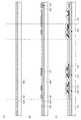
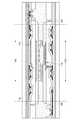
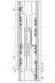
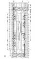
図1に、本発明の一態様であるタッチパネル100の構成を説明する投影図を示す。また図2に、図1に示すタッチパネル100の一点鎖線A1―A2における断面図を示す。なお、図1及び図2は明瞭化のため、構成要素の一部を省略して示している。[Touch panel configuration example]
Fig. 1 shows a projection view illustrating a configuration of a
タッチパネル100は、画像表示装置180と、入力装置190と、を備える(図2参照)。The
タッチパネル100は、第1の基板121の第2の基板101に対向する側の面上に、検知部106、走査線駆動回路107、変換器108、外部接続端子109及びクラック抑止領域110を有する。クラック抑止領域110は、検知部106を囲うようにして設けられている。The
ここで、クラック抑止領域110は、後述するクラック抑止層を一以上含む領域である。Here, the
タッチパネル100は、第1の基板121と第2の基板101が封止層153を介して対向している。第1の基板121は接着層125を介して第1のバッファ層(被剥離層ともいう。以下、単にバッファ層と表記する)120を有し、バッファ層120上に検知部や変換器などを構成するトランジスタ(116,117及び129)、検知素子118が設けられる。また、バッファ層120に接して複数のクラック抑止層122を含むクラック抑止領域110が設けられる。また、第2の基板101は接着層131を介して第2のバッファ層132を有し、第2のバッファ層132上に表示素子として機能する発光素子114や、表示部102、走査線駆動回路104などを構成するトランジスタ、外部接続端子105が設けられる。In the
なお、第1の基板121及び第2の基板101は、可撓性基板であることが好ましい。It is preferable that the
バッファ層120及び第2のバッファ層132は、基板(第1の基板121及び第2の基板101)や接着層(接着層125及び接着層131)を透過した不純物がトランジスタや発光素子114等に拡散することを抑制する機能を有する。The
バッファ層120は、不純物の発光素子114への拡散を防ぐバリア膜としての機能を有する。バッファ層120としては、例えば無機材料の単膜やその積層膜を用いることができる。このような材料を用いることで、第1の基板121にバリア性能、とくに防湿性の低い材料を用いた場合でも、タッチパネルの防湿性を高めることができる。The
しかし、無機膜はぜい性破壊が起きやすく、タッチパネル100を湾曲させるなどした場合に、バッファ層120にクラックが発生することがある。また、透湿性の低い無機膜は膨潤率が低いため、例えばタッチパネル100が高温高湿環境下に置かれた場合に、バッファ層120と比べてその近傍の層がより大きく膨潤することにより、バッファ層120の隣接する層との界面に応力集中が起こり、クラックが発生することがある。However, inorganic films are prone to brittle fracture, and cracks may occur in the
そこで、バッファ層120に接するように、バッファ層120を構成する無機膜とは異なる材料で形成されるクラック抑止層を設けることで、バッファ層120に発生したクラックの進行を抑制することができる。Therefore, by providing a crack prevention layer made of a material different from the inorganic film that constitutes the
クラック抑止層122としては、無機膜よりも展延性が高く、かつ膨潤率が低い導電膜を好適に用いることができる。A conductive film that has higher ductility and a lower swelling rate than an inorganic film can be preferably used as the
また、クラック抑止層122として、無機膜に対して密着性の高い樹脂材料を用いることで、バッファ層120の表面で起こる応力集中をその界面で緩和することができるため好ましい。In addition, it is preferable to use a resin material that has high adhesion to inorganic films as the
クラック抑止領域110は、2つのクラック抑止層122で構成されている。図1にあるように、一のクラック抑止層122は検知部106を囲い、且つ上面から見て閉じた一の曲線(閉曲線、または端部が一致した曲線ともいう)を形成している。また、クラック抑止層122は、検知部106及び外部接続端子109を囲い、且つ上面から見て閉じた一の曲線(閉曲線、または端部が一致した曲線ともいう)を形成していてもよい。The
このように検知部106の周囲を囲うように設けられたクラック抑止領域110により、大型の基板を用いて複数のタッチパネル100を同時に作製した後にそれぞれ分断するような場合に、バッファ層120の端部に発生するクラックが、クラック抑止領域110の内側に進行することを抑制できる。The
また、後述するように、タッチパネル100は支持基板を剥離する工程を経ることにより作製することができる。このとき、剥離が基板端部から進行する際にバッファ層120に生じるクラックが、クラック抑止領域110の内側に進行することを抑制できる。As described below, the
なお、本構成例ではクラック抑止層122を第1の基板121の面上、すなわち第1のバッファ層120に重なるように検知部106の周囲に設けているが、クラック抑止層を第2の基板101の面上に設けてもよい。すなわち、クラック抑止層122を第2のバッファ層132に重なるように表示部102の周囲に設けることで、バッファ層132に発生したクラックの進行を抑制することができる。また、クラック抑止層を第1の基板121の面上及び第2の基板101の面上の両側に設けてもよい。In this configuration example, the
また、図1や図2ではクラック抑止領域110が検知部106を囲う閉曲線となるように設ける構成を示しているが(図16(A)参照)、クラック抑止領域110は必ずしも閉曲線となるように配置しなくてもよく、複数の線分に分断されていてもよい(図16(B)参照)。なお、図16(A)は図1において破線で囲んだ領域150内のクラック抑止領域110の拡大上面図である。また図16(B)はクラック抑止領域110を構成するクラック抑止層122が、複数の線分に分断されている一例を示す拡大上面図である。In addition, although Fig. 1 and Fig. 2 show a configuration in which the
以下では、図1及び図2を参照して、タッチパネル100のそのほかの構成について説明する。The rest of the configuration of the
外部接続端子105は、画像表示装置180内のトランジスタ(トランジスタ112、113、119)または発光素子114を構成する導電層と同一の材料で構成すると、作製工程を簡略化できるため好ましい。本構成例では、トランジスタのソース電極またはドレイン電極を構成する電極136及び第1の電極143と同一の材料で構成する例を示している。画像表示装置180には、外部接続端子105に異方性導電フィルム(ACF:Anisotropic Conductive Film)や、異方性導電ペースト(ACP:Anisotropic Conductive Paste)などを介してFPC(Flexible Printed Circuits)やICを実装することにより、信号を入力することができる。本構成例では、接続体156を介してFPC155が設けられている。It is preferable that the
また、入力装置190の外部接続端子109には接続体157を介してFPC128が接続されている。Furthermore, the
図2には、画像表示装置180を構成する走査線駆動回路104の一部として、トランジスタ119を有する例を示している。走査線駆動回路104としては、例えばnチャネル型のトランジスタとpチャネル型のトランジスタとを組み合わせた回路、nチャネル型のトランジスタで構成された回路、pチャネル型のトランジスタで構成された回路などを有していてもよい。また、本構成例では、表示部102が形成される第2のバッファ層132上に走査線駆動回路104が形成され、信号線駆動回路は駆動回路用ICを用いて第2の基板101に実装する構成を示しているが、走査線駆動回路と信号線駆動回路の両方を第2のバッファ層132上に形成するドライバ一体型の構成としてもよい。Figure 2 shows an example in which a
また、図2には、表示部102の一例として一画素分の断面構造を示している。画素は、電流制御用のトランジスタ112と、スイッチング用のトランジスタ113と、電流制御用のトランジスタ112が備える一対の電極136の一方と電気的に接続された第1の電極143を含む。また第1の電極143の端部を覆う絶縁層144が設けられている。2 shows a cross-sectional structure of one pixel as an example of the
画像表示装置180が備えるトランジスタ(トランジスタ112、113、119)は、ボトムゲート型のトランジスタである例を示している。各トランジスタは、チャネルとして機能する領域を含む半導体層135と、ゲート電極133と、ゲート絶縁膜として機能する絶縁層134と、を有する。また半導体層135と接するように一対の電極136が設けられ、半導体層135及び電極136を覆うように絶縁層141及び絶縁層142が設けられている。なお、半導体層135において、チャネルとして機能する領域を挟んで低抵抗な領域が設けられていてもよい。In this example, the transistors (
発光素子114は、絶縁層142上に第1の電極143、EL層151、第2の電極152が順に積層された積層構造を有している。本構成例で例示する画像表示装置180はトップエミッション方式の表示装置であるため、第2の電極152に透光性の材料を用いる。また第1の電極143には反射性の材料を用いることが好ましい。EL層151は少なくとも発光性の有機化合物を含む。EL層151を挟持する第1の電極143と第2の電極152の間に電圧を印加し、EL層151に電流を流すことにより、発光素子114を発光させることができる。The light-emitting
第2の基板101と対向するように第1の基板121が設けられ、第2の基板101と第1の基板121とが、封止層153により接着されている。The
入力装置190が備えるトランジスタ(トランジスタ116、117、129)は、トランジスタ112等と同様にボトムゲート型のトランジスタである例を示している。各トランジスタは、チャネルとして機能する領域を含む半導体層173と、ゲート電極171と、ゲート絶縁膜として機能する絶縁層172と、を有する。また半導体層173と接するように一対の電極174が設けられ、半導体層173及び電極174を覆うように絶縁層175が設けられている。なお、半導体層173において、チャネルとして機能する領域を挟んで低抵抗な領域が設けられていてもよい。なお、入力装置190が備えるトランジスタは、画像表示装置180が備えるトランジスタと異なっていてもよい。The transistors (
検知素子118は、絶縁層175上に導電層176、絶縁層177、導電層178が順に積層された積層構造を有している。検知素子118は複数の発光素子114と重なる位置に設けられているため、導電層176及び導電層178には透光性の材料を用いる。導電層176及び導電層178は検知素子118における一対の電極として機能し、絶縁層177は誘電体として機能することができる。The
導電層178上には絶縁層179が設けられる。絶縁層179上には、発光素子114と重なる位置にカラーフィルタ127が設けられ、絶縁層144と重なる位置にブラックマトリクス126が設けられる。An insulating
[材料及び形成方法について]
以下では、上述した各要素に用いることのできる材料及び形成方法について説明する。[Materials and Forming Method]
The following describes materials and formation methods that can be used for each of the above-mentioned elements.
〔可撓性基板〕
可撓性基板の材料としては、有機樹脂や可撓性を有する程度に薄いガラス材料などを用いることができる。[Flexible Substrate]
The flexible substrate may be made of an organic resin or a glass material that is thin enough to be flexible.
例えば、ポリエチレンテレフタレート(PET)、ポリエチレンナフタレート(PEN)等のポリエステル樹脂、ポリアクリロニトリル樹脂、ポリイミド樹脂、ポリメチルメタクリレート樹脂、ポリカーボネート(PC)樹脂、ポリエーテルスルホン(PES)樹脂、ポリアミド樹脂、シクロオレフィン樹脂、ポリスチレン樹脂、ポリアミドイミド樹脂、ポリ塩化ビニル樹脂等が挙げられる。特に、熱膨張係数の低い材料を用いることが好ましく、例えば、熱膨張係数が30×10−6/K以下であるポリアミドイミド樹脂、ポリイミド樹脂、PET等を好適に用いることができる。また、繊維体に樹脂を含浸した基板(プリプレグとも記す)や、無機フィラーを有機樹脂に混ぜて熱膨張係数を下げた基板を使用することもできる。 Examples of the material include polyester resins such as polyethylene terephthalate (PET) and polyethylene naphthalate (PEN), polyacrylonitrile resins, polyimide resins, polymethyl methacrylate resins, polycarbonate (PC) resins, polyethersulfone (PES) resins, polyamide resins, cycloolefin resins, polystyrene resins, polyamideimide resins, polyvinyl chloride resins, etc. In particular, it is preferable to use a material with a low thermal expansion coefficient, and for example, polyamideimide resins, polyimide resins, PET, etc., with a thermal expansion coefficient of 30×10−6 /K or less can be suitably used. In addition, a substrate in which a fiber body is impregnated with a resin (also referred to as a prepreg) or a substrate in which an inorganic filler is mixed with an organic resin to reduce the thermal expansion coefficient can also be used.
上記材料中に繊維体が含まれている場合、繊維体は有機化合物または無機化合物の高強度繊維を用いる。高強度繊維とは、具体的には引張弾性率またはヤング率の高い繊維のことを言い、代表例としては、ポリビニルアルコール系繊維、ポリエステル系繊維、ポリアミド系繊維、ポリエチレン系繊維、アラミド系繊維、ポリパラフェニレンベンゾビスオキサゾール繊維、ガラス繊維、または炭素繊維が挙げられる。ガラス繊維としては、Eガラス、Sガラス、Dガラス、Qガラス等を用いたガラス繊維が挙げられる。これらは、織布または不織布の状態で用い、この繊維体に樹脂を含浸させ樹脂を硬化させた構造物を可撓性を有する基板として用いてもよい。可撓性を有する基板として、繊維体と樹脂からなる構造物を用いると、曲げや局所的押圧による破損に対する信頼性が向上するため、好ましい。When the above-mentioned material contains a fibrous body, the fibrous body is made of high-strength fibers of organic or inorganic compounds. High-strength fibers specifically refer to fibers with a high tensile modulus or Young's modulus, and representative examples include polyvinyl alcohol fibers, polyester fibers, polyamide fibers, polyethylene fibers, aramid fibers, polyparaphenylene benzobisoxazole fibers, glass fibers, and carbon fibers. Examples of glass fibers include glass fibers using E glass, S glass, D glass, Q glass, etc. These may be used in the form of woven or nonwoven fabric, and a structure in which the fibrous body is impregnated with resin and the resin is hardened may be used as a flexible substrate. It is preferable to use a structure made of a fibrous body and resin as a flexible substrate, since this improves reliability against breakage due to bending or local pressure.
発光素子114からの光を取り出す側の可撓性を有する基板には、EL層151からの発光に対して透光性を有する材料を用いる。光射出側に設ける材料において、光の取り出し効率向上のためには、可撓性及び透光性を有する材料の屈折率は高い方が好ましい。例えば、有機樹脂に屈折率の高い無機フィラーを分散させることで、該有機樹脂のみからなる基板よりも屈折率の高い基板を実現できる。特に粒子径40nm以下の小さな無機フィラーを使用すると、光学的な透明性を失わないため、好ましい。For the flexible substrate on the side from which light from the light-emitting
また、光射出側とは反対側に設ける基板は、透光性を有していなくてもよいため、上記に挙げた基板の他に、金属基板または合金基板等を用いることもできる。基板の厚さは、可撓性や曲げ性を得るために、10μm以上200μm以下、好ましくは20μm以上50μm以下であることが好ましい。基板を構成する材料としては、特に限定はないが、例えば、アルミニウム、銅、ニッケル、または、アルミニウム合金もしくはステンレス等の金属の合金などを好適に用いることができる。光を取り出さない側の可撓性を有する基板に、金属または合金材料を含む導電性の基板を用いると、発光素子114からの発熱に対する放熱性が高まるため好ましい。The substrate provided on the side opposite to the light emission side does not need to be light-transmitting, and therefore, in addition to the substrates listed above, a metal substrate or an alloy substrate can be used. In order to obtain flexibility and bendability, the thickness of the substrate is preferably 10 μm to 200 μm, and more preferably 20 μm to 50 μm. There are no particular limitations on the material constituting the substrate, but for example, aluminum, copper, nickel, or an alloy of a metal such as an aluminum alloy or stainless steel can be suitably used. It is preferable to use a conductive substrate containing a metal or alloy material as the flexible substrate on the side from which light is not extracted, since this enhances the heat dissipation properties against the heat generated by the light-emitting
また、導電性を有する基板を用いる場合には、基板の表面を酸化する、または表面に絶縁膜を形成するなどし、絶縁処理が施された基板を用いることが好ましい。例えば、電着法、スピンコート法やディップ法などの塗布法、スクリーン印刷法などの印刷法、蒸着法やスパッタリング法、堆積法などの方法を用いて導電性の基板表面に絶縁膜を形成してもよいし、酸素雰囲気下で放置または加熱する方法や、陽極酸化法などの方法により、基板の表面を酸化してもよい。When using a conductive substrate, it is preferable to use a substrate that has been subjected to an insulating treatment, such as by oxidizing the surface of the substrate or forming an insulating film on the surface. For example, an insulating film may be formed on the conductive substrate surface using a coating method such as electrodeposition, spin coating or dipping, a printing method such as screen printing, a vapor deposition method, a sputtering method, or a deposition method, or the substrate surface may be oxidized by leaving or heating in an oxygen atmosphere, or by anodizing.
また、可撓性を有する基板の表面に凹凸形状を有する場合、該凹凸形状を被覆して平坦化した絶縁表面を形成するために平坦化層を設けてもよい。平坦化層としては絶縁性の材料を用いることができ、有機材料または無機材料で形成することができる。例えば、平坦化層は、スパッタリング法などの堆積法、スピンコート法やディップ法などの塗布法、インクジェット法やディスペンス法などの吐出法、スクリーン印刷法などの印刷法等を用いて形成することができる。In addition, when the surface of a flexible substrate has an uneven shape, a planarizing layer may be provided to cover the uneven shape and form a flat insulating surface. An insulating material may be used as the planarizing layer, and the planarizing layer may be formed of an organic material or an inorganic material. For example, the planarizing layer may be formed by a deposition method such as sputtering, a coating method such as spin coating or dipping, a discharge method such as inkjet or dispensing, a printing method such as screen printing, or the like.
また、可撓性を有する基板として、複数の層を積層した材料を用いることもできる。例えば有機樹脂からなる層を2種類以上積層した材料、有機樹脂からなる層と無機材料からなる層を積層した材料、無機材料からなる層を2種類以上積層した材料などを用いる。無機材料からなる層を設けることにより、水分等の内部への浸入が抑制されるため、タッチパネルの信頼性を向上させることができる。A material having multiple laminated layers can also be used as a flexible substrate. For example, a material having two or more laminated layers made of organic resin, a material having a laminated layer made of organic resin and a layer made of inorganic material, or a material having two or more laminated layers made of inorganic material can be used. By providing a layer made of inorganic material, the intrusion of moisture and the like into the interior can be suppressed, improving the reliability of the touch panel.
上記無機材料としては、金属や半導体の酸化物材料や窒化物材料、酸化窒化物材料などを用いることができる。例えば、酸化シリコン、窒化シリコン、酸化窒化シリコン、酸化アルミニウム、窒化アルミニウム、酸化窒化アルミニウムなどを用いればよい。なお、本明細書中において、窒化酸化とは、その組成として、酸素よりも窒素の含有量が多いものであって、酸化窒化とは、その組成として、窒素よりも酸素の含有量が多いものを示す。なお、各元素の含有量は、例えば、ラザフォード後方散乱分光法(RBS)等を用いて測定することができる。As the inorganic material, metal or semiconductor oxide materials, nitride materials, oxynitride materials, etc. can be used. For example, silicon oxide, silicon nitride, silicon oxynitride, aluminum oxide, aluminum nitride, aluminum oxynitride, etc. can be used. In this specification, oxynitride refers to a composition in which the nitrogen content is greater than the oxygen content, and oxynitride refers to a composition in which the oxygen content is greater than the nitrogen content. The content of each element can be measured, for example, using Rutherford backscattering spectroscopy (RBS) or the like.
例えば、有機樹脂からなる層と無機材料からなる層を積層する場合、有機樹脂からなる層の上層または下層に、スパッタリング法、CVD(Chemical Vapor Deposition)法または塗布法などにより、上記無機材料からなる層を形成することができる。For example, when laminating a layer made of an organic resin and a layer made of an inorganic material, a layer made of the inorganic material can be formed on or under the layer made of the organic resin by a sputtering method, a CVD (Chemical Vapor Deposition) method, a coating method, or the like.
また、可撓性を有する基板として、可撓性を有する程度に薄いガラス基板を用いてもよい。特に発光素子114に近い側から有機樹脂層、接着層、及びガラス層を積層したシートを用いることが好ましい。該ガラス層の厚さとしては20μm以上200μm以下、好ましくは25μm以上100μm以下の厚さとする。このような厚さのガラス層は、水や酸素に対する高いバリア性と可撓性を同時に実現できる。また、有機樹脂層の厚さとしては、10μm以上200μm以下、好ましくは20μm以上50μm以下とする。このような有機樹脂層をガラス層と接して設けることにより、ガラス層の割れやクラックを抑制し、機械的強度を向上させることができる。このようなガラス材料と有機樹脂の複合材料を、可撓性を有する基板に適用することにより、極めて信頼性が高く、且つフレキシブルなタッチパネルとすることができる。In addition, a glass substrate thin enough to have flexibility may be used as the substrate having flexibility. In particular, it is preferable to use a sheet in which an organic resin layer, an adhesive layer, and a glass layer are laminated from the side close to the
なお、ガラス基板などの可撓性を有しない基板を用いてもよい。In addition, a non-flexible substrate such as a glass substrate may also be used.
〔発光素子〕
発光素子としては、自発光が可能な素子を用いることができ、電流又は電圧によって輝度が制御される素子をその範疇に含む。例えば、発光ダイオード(LED)、有機EL素子、無機EL素子等を用いることができる。[Light-emitting element]
The light-emitting element may be an element capable of self-emitting light, and may include an element whose luminance is controlled by a current or a voltage. For example, a light-emitting diode (LED), an organic EL element, an inorganic EL element, etc. may be used.
本実施の形態の画像表示装置180が有する発光素子114は、一対の電極(第1の電極143及び第2の電極152)と、該一対の電極間に設けられたEL層151とを有する。該一対の電極の一方は陽極として機能し、他方は陰極として機能する。The light-emitting
発光素子114において、光射出側に設ける電極にはEL層151からの発光に対して透光性を有する材料を用いる。In the light-emitting
透光性を有する材料としては、酸化インジウム、酸化インジウム酸化スズ、酸化インジウム酸化亜鉛、酸化亜鉛、ガリウムを添加した酸化亜鉛などを用いることができる。または、グラフェンを用いてもよい。また、上記導電層として、金、銀、白金、マグネシウム、ニッケル、タングステン、クロム、モリブデン、鉄、コバルト、銅、パラジウム、またはチタンなどの金属材料や、これらを含む合金を用いることができる。または、これら金属材料の窒化物(例えば、窒化チタン)などを用いてもよい。なお、金属材料(またはその窒化物)を用いる場合には、透光性を有する程度に薄くすればよい。また、上記材料の積層膜を導電層として用いることができる。例えば、銀とマグネシウムの合金と酸化インジウム酸化スズの積層膜などを用いると、導電性を高めることができるため好ましい。As a material having light-transmitting properties, indium oxide, indium oxide tin oxide, indium oxide zinc oxide, zinc oxide, zinc oxide with gallium added, or the like can be used. Alternatively, graphene may be used. In addition, as the conductive layer, a metal material such as gold, silver, platinum, magnesium, nickel, tungsten, chromium, molybdenum, iron, cobalt, copper, palladium, or titanium, or an alloy containing these, can be used. Alternatively, a nitride of these metal materials (for example, titanium nitride) or the like may be used. Note that when a metal material (or its nitride) is used, it is sufficient to make it thin enough to have light-transmitting properties. Also, a laminated film of the above materials can be used as the conductive layer. For example, it is preferable to use a laminated film of an alloy of silver and magnesium and indium oxide tin oxide, etc., because it is possible to increase the conductivity.
このような電極は、蒸着法や、スパッタリング法などにより形成する。そのほか、インクジェット法などの吐出法、スクリーン印刷法などの印刷法、またはメッキ法を用いて形成することができる。Such electrodes are formed by deposition or sputtering. They can also be formed by ejection methods such as inkjet printing, printing methods such as screen printing, or plating.
なお、透光性を有する上述の導電性酸化物をスパッタリング法によって形成する場合、該導電性酸化物を、アルゴン及び酸素を含む雰囲気下で成膜すると、透光性を向上させることができる。When the above-mentioned conductive oxide having translucency is formed by a sputtering method, the translucency can be improved by forming the conductive oxide in an atmosphere containing argon and oxygen.
また導電性酸化物膜をEL層上に形成する場合、酸素濃度が低減されたアルゴンを含む雰囲気下で成膜した第1の導電性酸化物膜と、アルゴン及び酸素を含む雰囲気下で成膜した第2の導電性酸化物膜の積層膜とすると、EL層への成膜ダメージを低減できるため好ましい。ここで特に第1の導電性酸化物膜を成膜する際に用いるアルゴンガスの純度が高いことが好ましく、例えば露点が−70℃以下、好ましくは−100℃以下のアルゴンガスを用いる。When forming a conductive oxide film on an EL layer, it is preferable to form a laminate film of a first conductive oxide film formed in an atmosphere containing argon with a reduced oxygen concentration and a second conductive oxide film formed in an atmosphere containing argon and oxygen, since this reduces damage to the EL layer during film formation. Here, it is particularly preferable to use argon gas with a high purity when forming the first conductive oxide film, and for example, argon gas with a dew point of -70°C or less, preferably -100°C or less is used.
光射出側とは反対側に設ける電極には、EL層151からの発光に対して反射性を有する材料を用いることが好ましい。It is preferable to use a material that is reflective to the light emitted from the
光反射性を有する材料としては、例えばアルミニウム、金、白金、銀、ニッケル、タングステン、クロム、モリブデン、鉄、コバルト、銅、またはパラジウム等の金属、またはこれらを含む合金を用いることができる。またこれら金属材料を含む金属または合金にランタンやネオジム、ゲルマニウムなどを添加してもよい。そのほか、アルミニウムとチタンの合金、アルミニウムとニッケルの合金、アルミニウムとネオジムの合金などのアルミニウムを含む合金(アルミニウム合金)や、銀と銅の合金、銀とパラジウムと銅の合金、銀とマグネシウムの合金などの銀を含む合金を用いることもできる。銀と銅を含む合金は耐熱性が高いため好ましい。さらに、アルミニウム合金膜に接する金属膜、または金属酸化物膜を積層することで、アルミニウム合金膜の酸化を抑制することができる。該金属膜、金属酸化物膜の材料としては、チタン、酸化チタンなどが挙げられる。また、上記透光性を有する材料からなる膜と金属材料からなる膜とを積層してもよい。例えば、銀と酸化インジウム酸化スズの積層膜、銀とマグネシウムの合金と酸化インジウム酸化スズの積層膜などを用いることができる。As the material having light reflectivity, for example, metals such as aluminum, gold, platinum, silver, nickel, tungsten, chromium, molybdenum, iron, cobalt, copper, or palladium, or alloys containing these metals can be used. Lanthanum, neodymium, germanium, or the like may also be added to the metals or alloys containing these metal materials. In addition, alloys containing aluminum (aluminum alloys) such as an alloy of aluminum and titanium, an alloy of aluminum and nickel, or an alloy of aluminum and neodymium, or alloys containing silver such as an alloy of silver and copper, an alloy of silver, palladium, and copper, or an alloy of silver and magnesium can also be used. The alloys containing silver and copper are preferable because of their high heat resistance. Furthermore, by laminating a metal film or a metal oxide film in contact with the aluminum alloy film, oxidation of the aluminum alloy film can be suppressed. Examples of the material of the metal film or metal oxide film include titanium and titanium oxide. In addition, a film made of the above-mentioned material having light transmittance and a film made of a metal material may be laminated. For example, a laminate film of silver and indium oxide-tin oxide, a laminate film of an alloy of silver and magnesium and indium oxide-tin oxide, or the like can be used.
このような電極は、蒸着法や、スパッタリング法などにより形成する。そのほか、インクジェット法などの吐出法、スクリーン印刷法などの印刷法、またはメッキ法を用いて形成することができる。Such electrodes are formed by deposition or sputtering. They can also be formed by ejection methods such as inkjet printing, printing methods such as screen printing, or plating.
EL層151は、少なくとも発光性の有機化合物を含む層(以下、発光層ともいう)を含めばよく、単数の層で構成されていても、複数の層が積層されていてもよい。複数の層で構成されている構成としては、陽極側から正孔注入層、正孔輸送層、発光層、電子輸送層、並びに電子注入層が積層された構成を例に挙げることができる。なお、発光層を除くこれらの層はEL層151中に必ずしも全て設ける必要はない。また、これらの層は重複して設けることもできる。具体的にはEL層151中に複数の発光層を重ねて設けてもよく、電子注入層に重ねて正孔注入層を設けてもよい。また、中間層として電荷発生層の他、電子リレー層など他の構成を適宜加えることができる。また、例えば、異なる発光色を呈する発光層を複数積層する構成としてもよい。例えば補色の関係にある2以上の発光層を積層することにより白色発光を得ることができる。The
EL層151は、真空蒸着法、またはインクジェット法やディスペンス法などの吐出法、スピンコート法などの塗布法を用いて形成できる。The
〔封止層、接着層〕
封止層153としては、例えば、二液混合型樹脂、熱硬化性樹脂、光硬化性樹脂などの硬化性材料や、ゲルなどを用いることができる。例えば、エポキシ樹脂やアクリル樹脂、シリコーン樹脂、フェノール樹脂、ポリイミド、ポリビニルクロライド(PVC)、ポリビニルブチラル(PVB)、エチレンビニルアセテート(EVA)などを用いることができる。特に、エポキシ樹脂等の透湿性が低い材料が好ましい。[Sealing layer, adhesive layer]
For example, a curable material such as a two-part mixed resin, a thermosetting resin, or a photocurable resin, or a gel can be used as the
封止層153には乾燥剤が含まれていてもよい。例えば、アルカリ土類金属の酸化物(酸化カルシウムや酸化バリウム等)のように、化学吸着によって水分を吸着する物質を用いることができる。その他の乾燥剤として、ゼオライトやシリカゲル等のように、物理吸着によって水分を吸着する物質を用いてもよい。また、粒状の乾燥剤を設けることにより、該乾燥剤により発光素子114からの発光が乱反射されるため、信頼性が高く、且つ視野角依存性が改善した発光装置(特に照明用途等に有用)を実現できる。なお、接着層125及び接着層131としては、封止層153と同様の材料を用いることができる。The
〔トランジスタ〕
トランジスタ112、113、119、116、117、129の構造は特に限定されない。例えば、トランジスタの構成は、スタガ型のトランジスタ、逆スタガ型のトランジスタなどを用いてもよい。また、トップゲート型またはボトムゲート型のいずれのトランジスタ構造としてもよい。また、チャネルエッチ型のトランジスタ、または、チャネル保護型のトランジスタを用いてもよい。チャネル保護型の場合、チャネル領域の上にのみ、チャネル保護膜を設けてもよい。または、ソースドレイン電極と半導体層とを接触させる部分のみ開口し、その開口以外の場所にも、チャネル保護膜を設けてもよい。[Transistor]
The structures of the
トランジスタのチャネルが形成される半導体層に適用可能な半導体として、例えばシリコンやゲルマニウムなどの半導体材料、化合物半導体材料、有機半導体材料、または酸化物半導体材料を用いてもよい。As a semiconductor that can be used for the semiconductor layer in which the transistor channel is formed, for example, a semiconductor material such as silicon or germanium, a compound semiconductor material, an organic semiconductor material, or an oxide semiconductor material may be used.
また、トランジスタに用いる半導体の結晶性についても特に限定されず、非晶質半導体、結晶性を有する半導体(微結晶半導体、多結晶半導体、単結晶半導体、または一部に結晶領域を有する半導体)のいずれを用いてもよい。結晶性を有する半導体を用いると、トランジスタ特性の劣化が抑制されるため好ましい。The crystallinity of the semiconductor used in the transistor is not particularly limited, and any of an amorphous semiconductor and a semiconductor having crystallinity (a microcrystalline semiconductor, a polycrystalline semiconductor, a single crystal semiconductor, or a semiconductor having a crystalline region in part) may be used. The use of a semiconductor having crystallinity is preferable because it suppresses deterioration of the transistor characteristics.
例えば上記半導体としてシリコンを用いる場合、アモルファスシリコン、微結晶シリコン、多結晶シリコン、または単結晶シリコンなどを用いることができる。For example, when silicon is used as the semiconductor, amorphous silicon, microcrystalline silicon, polycrystalline silicon, or single crystal silicon can be used.
また、上記半導体として酸化物半導体を用いる場合、インジウム、ガリウム、亜鉛のうち少なくともひとつを含む酸化物半導体を用いることが好ましい。代表的にはIn−Ga−Zn系金属酸化物などが挙げられる。シリコンよりもバンドギャップが広く、且つキャリア密度の小さい酸化物半導体を用いると、オフ状態におけるリーク電流を抑制できるため好ましい。When an oxide semiconductor is used as the semiconductor, it is preferable to use an oxide semiconductor containing at least one of indium, gallium, and zinc. Representative examples include In-Ga-Zn-based metal oxides. It is preferable to use an oxide semiconductor that has a wider band gap and a smaller carrier density than silicon, because this can suppress leakage current in the off state.
〔バッファ層、絶縁層〕
バッファ層120は、第1の基板121や接着層125を透過した不純物が拡散することを抑制する機能を有する。第2のバッファ層132は、第2の基板101や接着層131を透過した不純物が拡散することを抑制する機能を有する。また、トランジスタの半導体層に接する絶縁層134、絶縁層172及びトランジスタを覆う絶縁層141、絶縁層175は、半導体層への不純物の拡散を抑制することが好ましい。これらの層には、例えばシリコンなどの半導体の酸化物または窒化物、アルミニウムなどの金属の酸化物または窒化物を用いることができる。また、このような無機絶縁材料の積層膜、または無機絶縁材料と有機絶縁材料の積層膜を用いてもよい。[Buffer layer, insulating layer]
The
上記無機絶縁材料としては、例えば窒化アルミニウム、酸化アルミニウム、窒化酸化アルミニウム、酸化窒化アルミニウム、酸化マグネシウム、酸化ガリウム、窒化シリコン、酸化シリコン、窒化酸化シリコン、酸化窒化シリコン、酸化ゲルマニウム、酸化ジルコニウム、酸化ランタン、酸化ネオジム、酸化タンタル等から選ばれた材料を、単層でまたは積層して形成する。The inorganic insulating material is formed in a single layer or in a multilayer structure using a material selected from the group consisting of aluminum nitride, aluminum oxide, aluminum nitride oxide, aluminum oxynitride, magnesium oxide, gallium oxide, silicon nitride, silicon oxide, silicon nitride oxide, silicon oxynitride, germanium oxide, zirconium oxide, lanthanum oxide, neodymium oxide, and tantalum oxide.
また、上記無機絶縁材料として、ハフニウムシリケート(HfSiOx)、窒素が添加されたハフニウムシリケート(HfSixOyNz)、窒素が添加されたハフニウムアルミネート(HfAlxOyNz)、酸化ハフニウム、酸化イットリウム等のhigh−k材料を用いてもよい。 Furthermore, the inorganic insulating material may be a high-k material such as hafnium silicate (HfSiOx ), nitrogen-added hafnium silicate (HfSix Oy Nz ), nitrogen-added hafnium aluminate (HfAlx Oy Nz ), hafnium oxide, or yttrium oxide.
絶縁層142及び絶縁層177は、トランジスタや配線などに起因する段差を被覆する平坦化層として機能する。例えばポリイミド、アクリル、ポリアミド、エポキシ等の有機樹脂や、無機絶縁材料を用いることができる。絶縁層142としては感光性の樹脂(アクリル、ポリイミドなど)を用いて形成することが好ましい。絶縁層177としては、感光性の樹脂のほか、上記の絶縁層134等と同様の材料を用いることができる。また、絶縁層144及び絶縁層179も、絶縁層142と同様の材料を用いて形成することができる。The insulating
〔クラック抑止層〕
クラック抑止層122は、導電性材料を用いて形成することができる。また、クラック抑止層122をトランジスタ116等のゲート電極171と同一の材料で形成することで、工程を簡略化できるため好ましい。[Crack prevention layer]
The
クラック抑止層122はこれと接して設けられるバッファ層120のクラックの進行を抑止するため、外部応力に強い導電性材料が好ましい。The
クラック抑止層122は、例えば、モリブデン、チタン、クロム、タンタル、タングステン、アルミニウム、銅、ネオジム、スカンジウム等の金属材料又はこれらの元素を含む合金材料を用いて、単層で又は積層して形成することができる。また、クラック抑止層122は、導電性の金属酸化物を用いて形成しても良い。The
また、クラック抑止層122は、バッファ層120に対して密着性の高い樹脂材料を用いてもよい。樹脂材料として、例えばポリイミド、アクリル、ポリアミド、エポキシ等が挙げられる。The
クラック抑止層122の厚さとしては、機械的強度が保持できる膜厚を選択する必要がある。具体的には、厚さ50nm以上1000nm以下で形成し、好ましくは100nm以上500nm以下で形成する。The thickness of the
また、クラック抑止層122の幅としては、クラックの進行を抑止できる幅が必要である。しかし、クラック抑止層122の幅を大きくすることで、多面取りによってタッチパネル100を作製する場合などにおいて、一の基板から所望のタッチパネルが取れる個数(取り数ともいう)が減少する可能性がある。具体的には、幅20μm以上1000μm以下で形成し、好ましくは50μm以上500μm以下で形成する。The width of the
〔導電層〕
検知素子118において、一対の電極として機能する導電層176及び導電層178には、透光性を有する材料を用いる。[Conductive Layer]
In the
透光性を有する材料としては、酸化インジウム、酸化インジウム酸化スズ、酸化インジウム酸化亜鉛、酸化亜鉛、ガリウムを添加した酸化亜鉛などを用いることができる。または、グラフェンを用いてもよい。また、上記導電層として、金、銀、白金、マグネシウム、ニッケル、タングステン、クロム、モリブデン、鉄、コバルト、銅、パラジウム、またはチタンなどの金属材料や、これらを含む合金を用いることができる。または、これら金属材料の窒化物(例えば、窒化チタン)などを用いてもよい。なお、金属材料(またはその窒化物)を用いる場合には、透光性を有する程度に薄くすればよい。また、上記材料の積層膜を導電層として用いることができる。例えば、銀とマグネシウムの合金と酸化インジウム酸化スズの積層膜などを用いると、導電性を高めることができるため好ましい。As a material having light-transmitting properties, indium oxide, indium oxide tin oxide, indium oxide zinc oxide, zinc oxide, zinc oxide with gallium added, or the like can be used. Alternatively, graphene may be used. In addition, as the conductive layer, a metal material such as gold, silver, platinum, magnesium, nickel, tungsten, chromium, molybdenum, iron, cobalt, copper, palladium, or titanium, or an alloy containing these, can be used. Alternatively, a nitride of these metal materials (for example, titanium nitride) or the like may be used. Note that when a metal material (or its nitride) is used, it is sufficient to make it thin enough to have light-transmitting properties. Also, a laminated film of the above materials can be used as the conductive layer. For example, it is preferable to use a laminated film of an alloy of silver and magnesium and indium oxide tin oxide, etc., because it is possible to increase the conductivity.
導電層176及び導電層178は、蒸着法や、スパッタリング法などにより形成する。そのほか、インクジェット法などの吐出法、スクリーン印刷法などの印刷法、またはメッキ法を用いて形成することができる。The
なお、透光性を有する上述の導電性酸化物をスパッタリング法によって形成する場合、該導電性酸化物を、アルゴン及び酸素を含む雰囲気下で成膜すると、透光性を向上させることができる。When the above-mentioned conductive oxide having translucency is formed by a sputtering method, the translucency can be improved by forming the conductive oxide in an atmosphere containing argon and oxygen.
また、後に変形例で示すように、導電層の一方に酸化物導電体を用いてもよい。Also, as shown in a modified example later, an oxide conductor may be used for one of the conductive layers.
〔接続体〕
接続体156としては、熱硬化性の樹脂に金属粒子を混ぜ合わせたペースト状又はシート状の材料を用い、熱圧着によって異方性の導電性を示す材料を用いることができる。金属粒子としては、例えばニッケル粒子を金で被覆したものなど、2種類以上の金属が層状となった粒子を用いることが好ましい。[Connector]
A paste-like or sheet-like material made of a thermosetting resin mixed with metal particles, which exhibits anisotropic conductivity when bonded by heat, can be used as the
〔カラーフィルタ及びブラックマトリクス〕
カラーフィルタ127は、発光素子114からの発光色を調色し、色純度を高める目的で設けられている。例えば、白色発光の発光素子を用いてフルカラーの画像表示装置180とする場合には、異なる色のカラーフィルタを設けた複数の画素を用いる。その場合、赤色(R)、緑色(G)、青色(B)の3色のカラーフィルタを用いてもよいし、これに黄色(Y)を加えた4色とすることもできる。また、R、G、B、(及びY)に加えて白色(W)の画素を用い、4色(または5色)としてもよい。[Color filter and black matrix]
The
また、隣接するカラーフィルタ127の間には、ブラックマトリクス126が設けられている。ブラックマトリクス126は隣接する画素の発光素子114から回り込む光を遮光し、隣接画素間における混色を抑制する。ここで、カラーフィルタ127の端部を、ブラックマトリクス126と重なるように設けることにより、光漏れを抑制することができる。ブラックマトリクス126は、発光素子114からの発光を遮光する材料を用いることができ、金属材料や、顔料を含む有機樹脂などを用いて形成することができる。なお、ブラックマトリクス126は、走査線駆動回路104などの表示部102以外の領域に設けてもよい。A
また、カラーフィルタ127及びブラックマトリクス126を覆うオーバーコートを設けてもよい。オーバーコートは、カラーフィルタ127やブラックマトリクス126を保護するほか、これらに含まれる不純物が拡散することを抑制する。オーバーコートは発光素子114からの発光を透過する材料から構成され、無機絶縁膜や有機絶縁膜を用いることができる。An overcoat may also be provided to cover the
また、本構成例ではカラーフィルタを設ける構成としたが、それぞれR、G、Bなど異なる色の発光を呈する発光素子のうちいずれか一を画素に配置し、カラーフィルタを設けない構成としてもよい。In addition, in this configuration example, a color filter is provided, but it is also possible to arrange one of the light-emitting elements that emit light of a different color, such as R, G, or B, in each pixel, and not provide a color filter.
以上が各要素についての説明である。That concludes the explanation of each element.
[作製方法例]
以下では、上記タッチパネル100の作製方法の一例について、図面を参照して説明する。[Example of manufacturing method]
An example of a method for producing the
図3乃至図8は、以下で説明するタッチパネル100の作製方法例での、各段階における断面概略図である。図3乃至図8は、図1、図2で示した箇所の断面構造に対応する。Figures 3 to 8 are schematic cross-sectional views at each stage in an example of a method for fabricating a
〔剥離層の形成〕
まず、支持基板161上に剥離層162を形成する。[Formation of release layer]
First, a
支持基板161としては、少なくとも後の工程にかかる熱に対して耐熱性を有する基板を用いる。支持基板161としては、例えばガラス基板、樹脂基板の他、半導体基板、金属基板、セラミック基板などを用いることができる。The
なお、量産性を向上させるため、支持基板161として大型のガラス基板を用いることが好ましい。例えば、第3世代(550mm×650mm)、第3.5世代(600mm×720mm、または620mm×750mm)、第4世代(680mm×880mm、または730mm×920mm)、第5世代(1100mm×1300mm)、第6世代(1500mm×1850mm)、第7世代(1870mm×2200mm)、第8世代(2200mm×2400mm)、第9世代(2400mm×2800mm、2450mm×3050mm)、第10世代(2950mm×3400mm)等のガラス基板、またはこれよりも大型のガラス基板を用いることができる。In order to improve mass productivity, it is preferable to use a large glass substrate as the
剥離層162としては、例えばタングステン、チタン、モリブデンなどの高融点金属材料を用いることができる。好ましくはタングステンを用いる。The
剥離層162は、例えばスパッタリング法により形成することができる。The
〔バッファ層の形成〕
続いて、剥離層162の上にバッファ層120を形成する(図3(A)参照)。[Formation of Buffer Layer]
Next, the
バッファ層120としては、酸化シリコン、酸化窒化シリコン、窒化酸化シリコン、窒化シリコン、酸化アルミニウムなどの無機絶縁材料を用いることができる。またバッファ層120としては、上記無機絶縁材料を含む層を単層で、もしくは積層で用いることができる。The
バッファ層120は、支持基板161の外から不純物が浸入することを防ぐバリア膜の機能を有する。また、後述するように加熱によって剥離層162に水素を放出する機能を有する。そのため、特に、バッファ層120として2層以上の積層構造とし、そのうち少なくとも1層には加熱により水素を放出する層を用い、剥離層162から見て該水素を放出する層よりも遠い層には水素などの不純物を透過しない層を用いることが好ましい。例えば、剥離層162から酸化窒化シリコンを含む層と、窒化シリコンを含む層の積層構造とする。The
バッファ層120は、スパッタリング法、プラズマCVD法などの成膜方法により形成できる。特に、水素を含む成膜ガスを用いたプラズマCVDにより成膜することが好ましい。The
ここで、バッファ層120の成膜時に剥離層162の表面が酸化されることにより、剥離層162とバッファ層120の間に酸化物(図示しない)が形成される。該酸化物は、剥離層162に含まれる金属の酸化物を含む層である。好ましくは、タングステン酸化物を含む層とする。Here, the surface of the
タングステン酸化物は一般にWO(3−x)で表記され、代表的にはWO3、W2O5、W4O11、WO2といった様々な組成をとりうる不定比性化合物である。またチタン酸化物(TiO(2−x))、やモリブデン酸化物(MoO(3−x))も不定比性化合物である。 Tungsten oxide is generally represented asWO(3-x) and is a non-stoichiometric compound that can have various compositions, typicallyWO3 ,W2O5,W4O11 , andWO2 . Titanium oxide (TiO(2-x) ) and molybdenum oxide (MoO(3-x) ) are also non-stoichiometric compounds.
この段階における酸化物層は、酸素を多く含む状態であることが好ましい。例えば剥離層162としてタングステンを用いた場合には、酸化物層がWO3を主成分とするタングステン酸化物であることが好ましい。 The oxide layer at this stage preferably contains a large amount of oxygen. For example, when tungsten is used as the
ここで、バッファ層120の形成前に、剥離層162の表面に対して酸化性ガス、好ましくは一酸化二窒素ガスを含む雰囲気下でプラズマ処理を施し、剥離層162の表面に予め酸化物層を形成することもできる。このような方法を用いると、酸化物層の厚さをプラズマ処理の条件を異ならせることで変化させることができ、プラズマ処理を行わない場合に比べて酸化物層の厚さの制御性を高めることができる。Here, before forming the
酸化物層の厚さは、例えば0.1nm以上100nm以下、好ましくは0.5nm以上20nm以下とする。なお、酸化物層が極めて薄い場合には、断面観察像では観察されない場合がある。The thickness of the oxide layer is, for example, 0.1 nm to 100 nm, preferably 0.5 nm to 20 nm. If the oxide layer is extremely thin, it may not be observed in the cross-sectional observation image.
〔加熱処理〕
続いて、加熱処理を行い、酸化物層を変質させる。加熱処理を行うことにより、バッファ層120から水素が放出され、酸化物層に供給される。[Heat Treatment]
Subsequently, a heat treatment is performed to transform the oxide layer, whereby hydrogen is released from the
酸化物層に供給された水素により、酸化物層内の金属酸化物が還元され、酸化物層中に酸素の組成の異なる領域が複数混在した状態となる。例えば、剥離層162としてタングステンを用いた場合には、酸化物層中のWO3が還元されてこれよりも酸素の組成の少ない状態(例えばWO2など)が生成され、これらが混在した状態となる。このような金属酸化物は酸素の組成に応じて異なる結晶構造を示すため、酸化物層内に酸素の組成が異なる複数の領域を形成することで酸化物層の機械的強度が脆弱化する。その結果、酸化物層の内部で崩壊しやすい状態が実現され、後の剥離工程における剥離性を向上させることができる。 The hydrogen supplied to the oxide layer reduces the metal oxide in the oxide layer, resulting in a state in which multiple regions with different oxygen compositions are mixed in the oxide layer. For example, when tungsten is used as the
加熱処理は、バッファ層120から水素が脱離する温度以上、支持基板161の軟化点以下で行えばよい。また酸化物層内の金属酸化物と水素の還元反応が生じる温度以上で行うことが好ましい。例えば、剥離層162にタングステンを用いる場合には、420℃以上、450℃以上、600℃以上、または650℃以上の温度で加熱する。The heat treatment may be performed at a temperature equal to or higher than the temperature at which hydrogen is released from the
加熱処理の温度が高いほど、バッファ層120からの水素の脱離量が高まるため、その後の剥離性を向上させることができる。しかし、支持基板161の耐熱性や、生産性を考慮して加熱温度を低くしたい場合には、上述のように予め剥離層162に対してプラズマ処理を施して酸化物層を形成することにより、加熱処理の温度を低くしても高い剥離性を実現できる。The higher the temperature of the heat treatment, the greater the amount of hydrogen released from the
〔ゲート電極及びクラック抑止層の形成〕
続いて、バッファ層120上に導電膜を成膜する。その後、導電膜上にフォトリソグラフィ法等を用いてレジストマスクを形成し、導電膜の不要な部分をエッチングにより除去する。その後レジストマスクを除去することにより、ゲート電極171及び複数のクラック抑止層122からなるクラック抑止領域110を形成する。[Formation of gate electrode and crack prevention layer]
Next, a conductive film is formed on the
なお、このとき回路を構成する配線なども同時に形成してもよい。At this time, wiring that constitutes the circuit may also be formed at the same time.
ゲート電極171となる導電膜は、スパッタリング法、蒸着法、CVD法などにより成膜する。The conductive film that will become the
なお、クラック抑止層122はゲート電極171と同時に形成しなくてもよく、ゲート電極171と異なる材料を用いてもよい。The
〔ゲート絶縁層の形成〕
続いて、ゲート電極171を覆って絶縁層172を形成する。このとき、外部接続端子109となる配線、及び該配線の走査線駆動回路用のトランジスタ129の一方の電極174と接続する箇所のそれぞれに達する開口部を絶縁層172に形成する(図3(B)参照)。[Formation of Gate Insulating Layer]
Subsequently, an insulating
絶縁層172は、プラズマCVD法、スパッタリング法などにより形成することができる。The insulating
なお、本作製方法例では半導体層173上に形成される絶縁層として、絶縁層172の単層を形成する構成としたが、これに限られず2層以上の積層構造としてもよい。In this example of the manufacturing method, a single layer of insulating
〔半導体層の形成〕
続いて、絶縁層172上に半導体層を成膜する。その後、半導体膜上にフォトリソグラフィ法等を用いてレジストマスクを形成し、半導体膜の不要な部分をエッチングにより除去する。その後レジストマスクを除去することにより、トランジスタを構成する半導体層173を形成する。[Formation of Semiconductor Layer]
Next, a semiconductor layer is formed over the insulating
半導体膜の成膜は、用いる材料に応じて適切な方法を用いればよいが、例えばスパッタリング法、CVD法、MBE法、ALD(Atomic Layer Deposition)法、またはPLD(Pulsed Laser Deposition)法等を用いることができる。The semiconductor film can be formed by a method appropriate for the material used, such as sputtering, CVD, MBE, ALD (Atomic Layer Deposition), or PLD (Pulsed Laser Deposition).
半導体層に用いる半導体としては、酸化物半導体を用いることが好ましい。特にシリコンよりもバンドギャップの大きな酸化物半導体を適用することが好ましい。シリコンよりもバンドギャップが広く、且つキャリア密度の小さい半導体材料を用いると、トランジスタのオフ状態における電流を低減できるため好ましい。It is preferable to use an oxide semiconductor as the semiconductor used in the semiconductor layer. In particular, it is preferable to use an oxide semiconductor having a larger band gap than silicon. It is preferable to use a semiconductor material having a wider band gap than silicon and a smaller carrier density because it is possible to reduce the current in the off state of the transistor.
例えば、上記酸化物半導体として、少なくともインジウム(In)もしくは亜鉛(Zn)を含むことが好ましい。より好ましくは、In−M−Zn系酸化物(MはAl、Ti、Ga、Ge、Y、Zr、Sn、La、CeまたはHf等の金属)で表記される酸化物を含む。For example, the oxide semiconductor preferably contains at least indium (In) or zinc (Zn). More preferably, the oxide semiconductor contains an oxide represented by In-M-Zn oxide (M is a metal such as Al, Ti, Ga, Ge, Y, Zr, Sn, La, Ce, or Hf).
特に、半導体層として、複数の結晶部を有し、当該結晶部はc軸が半導体層の被形成面、または半導体層の上面に対し垂直に配向し、且つ隣接する結晶部間には粒界を有さない酸化物半導体膜を用いることが好ましい。In particular, it is preferable to use an oxide semiconductor film as the semiconductor layer, which has multiple crystal parts whose c-axes are oriented perpendicular to the surface on which the semiconductor layer is formed or the upper surface of the semiconductor layer, and which has no grain boundaries between adjacent crystal parts.
このような酸化物半導体は、結晶粒界を有さないために表示パネルを湾曲させたときの応力によって酸化物半導体膜にクラックが生じてしまうことが抑制される。したがって、可撓性を有し、湾曲させて用いる表示パネルなどに、このような酸化物半導体を好適に用いることができる。Since such oxide semiconductors do not have crystal grain boundaries, the occurrence of cracks in the oxide semiconductor film due to stress when the display panel is bent is suppressed. Therefore, such oxide semiconductors can be suitably used for display panels that are flexible and are used in a bent state.
また、半導体膜に多結晶シリコンを適用する場合には、アモルファスシリコンを成膜した後に結晶化(例えばレーザ光の照射や、熱処理など)を行い、多結晶シリコンを有する半導体膜を形成する。When polycrystalline silicon is used for the semiconductor film, the amorphous silicon is deposited and then crystallized (for example, by irradiation with laser light or heat treatment) to form a semiconductor film containing polycrystalline silicon.
〔ソース電極、ドレイン電極〕
続いて、絶縁層172及び半導体層173上に導電膜を成膜する。その後導電膜上にフォトリソグラフィ法等を用いてレジストマスクを形成し、導電膜の不要な部分をエッチングにより除去する。その後レジストマスクを除去することにより、トランジスタのソース電極またはドレイン電極として機能する電極174を形成する。[Source electrode, drain electrode]
Next, a conductive film is formed over the insulating
なおこのとき、回路を構成する配線なども同時に形成してもよい。本作製方法例では外部接続端子となる部分で該導電膜がゲート電極171と同一の導電膜上に形成される。At this time, wiring that constitutes the circuit may also be formed at the same time. In this example of the manufacturing method, the conductive film is formed on the same conductive film as the
導電膜はスパッタリング法、蒸着法、CVD法などにより成膜する。The conductive film is formed by sputtering, vapor deposition, CVD, etc.
また、この時点でトランジスタ116、トランジスタ117、及びトランジスタ129が形成される。Also at this point,
〔絶縁層の形成〕
続いて、絶縁層172、半導体層173及び電極174を覆う絶縁層175を成膜する。このとき、トランジスタ117の一方の電極174及び外部接続端子となる配線のそれぞれに達する開口部を絶縁層175に形成する(図3(C)参照)。[Formation of insulating layer]
Subsequently, an insulating
絶縁層175は、プラズマCVD法、スパッタリング法などにより形成することができる。The insulating
なお、本作製方法例では絶縁層172、半導体層173及び電極174上に形成される絶縁層として、絶縁層175の単層を形成する構成としたが、これに限られず2層以上の積層構造としてもよい。In this example of the manufacturing method, a single layer of insulating
〔電極及び絶縁層の形成〕
続いて、絶縁層175上に導電膜を成膜する。その後導電膜上にフォトリソグラフィ法等を用いてレジストマスクを形成し、導電膜の不要な部分をエッチングにより除去する。その後レジストマスクを除去することにより、検知素子118の一方の電極として機能する導電層176を形成する。[Formation of electrodes and insulating layers]
Next, a conductive film is formed over the insulating
なおこのとき、回路を構成する配線なども同時に形成してもよい。本作製方法例では外部接続端子となる部分で該導電膜が電極174と同一の導電膜上に形成することにより、外部接続端子109を形成する。At this time, wiring that constitutes the circuit may also be formed at the same time. In this example of the manufacturing method, the conductive film is formed on the same conductive film as the
導電膜はスパッタリング法、蒸着法、CVD法などにより成膜する。The conductive film is formed by sputtering, vapor deposition, CVD, etc.
続いて、絶縁層175及び導電層176上に絶縁層177を形成する。このとき、外部接続端子109に達する開口部を絶縁層177に形成する。Next, an insulating
また、検知部106となる領域を囲むように、絶縁層175に達する開口部を絶縁層177に形成してもよい。絶縁層177に有機樹脂を用いる場合は、検知部106となる領域を囲むように開口部を設けることで、絶縁層177を介して外部から水分が浸入することを抑制できる。本作製方法例では、支持基板161の端部と、走査線駆動回路107及び変換器108との間に、検知部106となる領域を囲むように開口部を設けている。Also, an opening reaching the insulating
絶縁層177は、プラズマCVD法、スパッタリング法などにより形成することができる。また、絶縁層177は、印刷法、インクジェット法、フォトリソグラフィ法などでそれぞれ形成することができる。The insulating
なお、本作製方法例では導電層176上に形成される絶縁層として、絶縁層177の単層を形成する構成としたが、これに限られず2層以上の積層構造としてもよい。In this example of the manufacturing method, a single layer of insulating
続いて、絶縁層177上に導電膜を成膜する。その後導電膜上にフォトリソグラフィ法等を用いてレジストマスクを形成し、導電膜の不要な部分をエッチングにより除去する。その後レジストマスクを除去することにより、検知素子118の他方の電極として機能する導電層178を形成する。Next, a conductive film is formed on the insulating
導電膜はスパッタリング法、蒸着法、CVD法などにより成膜する。The conductive film is formed by sputtering, vapor deposition, CVD, etc.
また、この時点で検知素子118が形成される(図4(A)参照)。Also, at this point, the
続いて、絶縁層177及び導電層178上に絶縁層179を形成する。このとき、外部接続端子109に達する開口部を絶縁層179に形成する。Next, an insulating
また、検知部106となる領域を囲むように、絶縁層175に達する開口部を絶縁層179に形成してもよい。本作製方法例では、支持基板161の端部と、走査線駆動回路107及び変換器108の間に、検知部106となる領域を囲むように開口部を設けている。Also, an opening reaching the insulating
絶縁層179は、プラズマCVD法、スパッタリング法などにより形成することができる。また、絶縁層179は、印刷法、インクジェット法、フォトリソグラフィ法などでそれぞれ形成することができる。The insulating
なお、本作製方法例では導電層178上に形成される絶縁層として、絶縁層179の単層を形成する構成としたが、これに限られず2層以上の積層構造としてもよい。In this example of the manufacturing method, a single layer of insulating
〔ブラックマトリクス及びカラーフィルタの形成〕
続いて、絶縁層179上にブラックマトリクス126及びカラーフィルタ127を形成する(図4(B)参照)。ブラックマトリクス126及びカラーフィルタ127は、印刷法、インクジェット法、フォトリソグラフィ法などでそれぞれ形成する。[Formation of Black Matrix and Color Filter]
Next, the
〔ゲート電極の形成〕
次に、剥離層164及び第2のバッファ層132を形成した支持基板163を準備する。剥離層164及び第2のバッファ層132の形成方法は前述の剥離層162及びバッファ層120と同様である。[Formation of Gate Electrode]
Next, a supporting
続いて、第2のバッファ層132上に導電膜を成膜する。その後、導電膜上にフォトリソグラフィ法等を用いてレジストマスクを形成し、導電膜の不要な部分をエッチングにより除去する。その後レジストマスクを除去することにより、ゲート電極133を形成する。Next, a conductive film is formed on the
なお、このとき回路を構成する配線なども同時に形成してもよい。At this time, wiring that constitutes the circuit may also be formed at the same time.
ゲート電極133となる導電膜は、スパッタリング法、蒸着法、CVD法などにより成膜する。The conductive film that will become the
〔ゲート絶縁層の形成〕
続いて、ゲート電極133を覆って絶縁層134を形成する。[Formation of Gate Insulating Layer]
Subsequently, an insulating
なお、このときゲート電極133と同一の導電膜で形成された回路を構成する配線に達する開口部を形成してもよい。At this time, an opening may be formed that reaches the wiring that constitutes the circuit, which is made of the same conductive film as the
絶縁層134は、プラズマCVD法、スパッタリング法などにより形成することができる。The insulating
〔半導体層の形成〕
続いて、絶縁層134上に半導体膜を成膜する。その後、半導体膜上にフォトリソグラフィ法等を用いてレジストマスクを形成し、半導体膜の不要な部分をエッチングにより除去する。その後レジストマスクを除去することにより、トランジスタを構成する半導体層135を形成する。[Formation of Semiconductor Layer]
Next, a semiconductor film is formed over the insulating
半導体膜の成膜は、用いる材料に応じて適切な方法を用いればよいが、例えばスパッタリング法、CVD法、MBE法、ALD(Atomic Layer Deposition)法、またはPLD(Pulsed Laser Deposition)法等を用いることができる。The semiconductor film can be formed by a method appropriate for the material used, such as sputtering, CVD, MBE, ALD (Atomic Layer Deposition), or PLD (Pulsed Laser Deposition).
半導体層に用いる半導体としては、酸化物半導体を用いることが好ましい。特にシリコンよりもバンドギャップの大きな酸化物半導体を適用することが好ましい。シリコンよりもバンドギャップが広く、且つキャリア密度の小さい半導体材料を用いると、トランジスタのオフ状態における電流を低減できるため好ましい。It is preferable to use an oxide semiconductor as the semiconductor used in the semiconductor layer. In particular, it is preferable to use an oxide semiconductor having a larger band gap than silicon. It is preferable to use a semiconductor material having a wider band gap than silicon and a smaller carrier density because it is possible to reduce the current in the off state of the transistor.
例えば、上記酸化物半導体として、少なくともインジウム(In)もしくは亜鉛(Zn)を含むことが好ましい。より好ましくは、In−M−Zn系酸化物(MはAl、Ti、Ga、Ge、Y、Zr、Sn、La、CeまたはHf等の金属)で表記される酸化物を含む。For example, the oxide semiconductor preferably contains at least indium (In) or zinc (Zn). More preferably, the oxide semiconductor contains an oxide represented by In-M-Zn oxide (M is a metal such as Al, Ti, Ga, Ge, Y, Zr, Sn, La, Ce, or Hf).
特に、半導体層として、複数の結晶部を有し、当該結晶部はc軸が半導体層の被形成面、または半導体層の上面に対し垂直に配向し、且つ隣接する結晶部間には粒界を有さない酸化物半導体膜を用いることが好ましい。In particular, it is preferable to use an oxide semiconductor film as the semiconductor layer, which has multiple crystal parts whose c-axes are oriented perpendicular to the surface on which the semiconductor layer is formed or the upper surface of the semiconductor layer, and which has no grain boundaries between adjacent crystal parts.
このような酸化物半導体は、結晶粒界を有さないために表示パネルを湾曲させたときの応力によって酸化物半導体膜にクラックが生じてしまうことが抑制される。したがって、可撓性を有し、湾曲させて用いる表示パネルなどに、このような酸化物半導体を好適に用いることができる。Since such oxide semiconductors do not have crystal grain boundaries, the occurrence of cracks in the oxide semiconductor film due to stress when the display panel is bent is suppressed. Therefore, such oxide semiconductors can be suitably used for display panels that are flexible and are used in a bent state.
また、半導体膜に多結晶シリコンを適用する場合には、アモルファスシリコンを成膜した後に結晶化(例えばレーザ光の照射や、熱処理など)を行い、多結晶シリコンを有する半導体膜を形成する。When polycrystalline silicon is used for the semiconductor film, the amorphous silicon is deposited and then crystallized (for example, by irradiation with laser light or heat treatment) to form a semiconductor film containing polycrystalline silicon.
〔ソース電極、ドレイン電極〕
続いて、絶縁層134及び半導体層135上に導電膜を成膜する。その後導電膜上にフォトリソグラフィ法等を用いてレジストマスクを形成し、導電膜の不要な部分をエッチングにより除去する。その後レジストマスクを除去することにより、トランジスタのソース電極またはドレイン電極として機能する電極136を形成する。[Source electrode, drain electrode]
Next, a conductive film is formed over the insulating
なおこのとき、回路を構成する配線なども同時に形成してもよい。At this time, wiring that constitutes the circuit may also be formed at the same time.
導電膜はスパッタリング法、蒸着法、CVD法などにより成膜する。The conductive film is formed by sputtering, vapor deposition, CVD, etc.
また、この時点でトランジスタ112、トランジスタ113、及びトランジスタ119が形成される(図5(A)参照)。At this point,
〔絶縁層の形成〕
続いて、絶縁層134、半導体層135及び電極136を覆う絶縁層141を成膜する。このとき、電流制御用のトランジスタ112の一方の電極136及び外部接続端子105となる配線のそれぞれに達する開口部を絶縁層141に形成する。[Formation of insulating layer]
Subsequently, an insulating
絶縁層141は、プラズマCVD法、スパッタリング法などにより形成することができる。The insulating
なお、本作製方法例では絶縁層134、半導体層135及び電極136上に形成される絶縁層として、絶縁層141の単層を積層する構成としたが、これに限られず2層以上の積層構造としてもよい。In this example of the manufacturing method, a single layer of insulating
〔平坦化層の形成〕
続いて、平坦化層として機能する絶縁層142を形成する。このとき、電流制御用のトランジスタ112の一方の電極136及び外部接続端子105となる配線のそれぞれに達する開口部を絶縁層142に形成する。[Formation of Planarizing Layer]
Subsequently, an insulating
また、表示部102となる領域を囲むように、絶縁層141に達する開口部を絶縁層142に形成してもよい。絶縁層142に有機樹脂を用いる場合は、表示部102となる領域を囲むように開口部を設けることで、絶縁層142を介して外部から水分等が浸入することを抑制できる。本作製方法例では、基板101の端部と走査線駆動回路104の間に、表示部102を囲むように開口部を設けている。Also, an opening reaching the insulating
絶縁層142は、例えば感光性の有機樹脂をスピンコート法などにより塗布した後、選択的に露光、現像を行って形成することが好ましい。このほかの形成方法としては、スパッタリング法、蒸着法、液滴吐出法(インクジェット法)、スクリーン印刷、オフセット印刷等などを用いればよい。The insulating
〔第1の電極の形成〕
続いて、絶縁層142上に導電膜を成膜する。その後導電膜上にフォトリソグラフィ法等を用いてレジストマスクを形成し、導電膜の不要な部分をエッチングにより除去する。その後レジストマスクを除去することにより、トランジスタ112の一方の電極136と電気的に接続する第1の電極143を形成する。[Formation of the first electrode]
Next, a conductive film is formed over the insulating
なおこのとき、回路を構成する配線なども同時に形成してもよい。本作製方法例では外部接続端子となる部分で電極136と同一の導電膜上に形成することにより、外部接続端子105を形成する。At this time, wiring that constitutes the circuit may also be formed at the same time. In this example of the manufacturing method, the
導電膜はスパッタリング法、蒸着法、CVD法などにより成膜する。The conductive film is formed by sputtering, vapor deposition, CVD, etc.
〔絶縁層の形成〕
続いて、第1の電極143の端部を覆う絶縁層144を形成する。このとき外部接続端子105に達する開口部を絶縁層144に形成する。[Formation of insulating layer]
Subsequently, an insulating
また、表示部102となる領域を囲むように、絶縁層141に達する開口部を絶縁層144に形成してもよい。本作製方法例では、基板101の端部と走査線駆動回路104の間に、表示部102を囲むように開口部を設けている。Also, an opening reaching the insulating
絶縁層144は、例えば感光性の有機樹脂をスピンコート法などにより塗布した後、選択的に露光、現像を行って形成することが好ましい。このほかの形成方法としては、スパッタリング法、蒸着法、液滴吐出法(インクジェット法)、スクリーン印刷、オフセット印刷等などを用いればよい。The insulating
なお、絶縁層144上に、絶縁層を設けてもよい。図2において、表示部102における絶縁層144上に該絶縁層を設けることで、第1の基板121と第2の基板101の間隔を調整することができる。該絶縁層は、絶縁層144と同様の材料を用いて形成することができる。Note that an insulating layer may be provided on the insulating
〔発光素子の形成〕
続いて、第1の電極143上にEL層151、第2の電極152を順次形成することにより、発光素子114を形成する(図5(B)参照)。[Formation of Light-Emitting Element]
Next, an
EL層151を構成する層は、それぞれ真空蒸着法、またはインクジェット法やディスペンス法などの吐出法、スピンコート法などの塗布法を用いて形成する。第2の電極152は蒸着法またはスパッタリング法などにより形成する。The layers constituting the
〔貼り合わせ〕
続いて、支持基板161の検知素子118が設けられた面または支持基板163の発光素子114が設けられた面に、封止層153を形成する。[Lamination]
Subsequently, a
封止層153は、例えばディスペンス法などの吐出法、スクリーン印刷法などの印刷法等を用いて硬化性樹脂を塗布した後、該樹脂に含まれる溶媒を揮発させる。The
このとき、支持基板161または支持基板163上に、検知部106または表示部102を囲うように接着層154を形成してもよい。接着層154は、封止層153の封止性能を補強するために設けることができる。接着層154は、封止層153と同様の方法により形成することができる。At this time, an adhesive layer 154 may be formed on the
続いて、支持基板161と支持基板163とを貼り合わせ、封止層153を硬化させることにより、支持基板161と支持基板163とを接着する(図6参照)。Next, the
〔剥離〕
続いて、支持基板163を剥離し、露出した第2のバッファ層132と第2の基板101を、接着層131を介して貼り合わせる。また、支持基板161を剥離し、露出したバッファ層120と第1の基板121を、接着層125を介して貼り合わせる(図7参照)。図7では、第2の基板101が外部接続端子109と重なる構成としたが、外部接続端子109と第2の基板101が重ならない構成としてもよい。また、図7では、第1の基板121が外部接続端子105と重ならない構成としたが、外部接続端子105と第1の基板121が重なる構成としてもよい。[Peeling]
Next, the
剥離の方法としては、例えば支持基板161を吸着ステージに固定し、剥離層164と第2のバッファ層132との間に剥離の起点を形成する。例えば、これらの間に刃物などの鋭利な形状の器具を差し込むことで剥離の起点を形成してもよい。また一部の領域に対してレーザ光を照射し、剥離層164の一部を溶解、蒸発、または熱的に破壊することで剥離の起点を形成してもよい。また液体(例えばアルコールや水、二酸化炭素を含む水など)を剥離層164の端部に滴下し、毛細管現象を利用して該液体を剥離層164と第2のバッファ層132の境界に浸透させることにより剥離の起点を形成してもよい。As a method of peeling, for example, the
次いで、剥離の起点が形成された部分において、密着面に対して略垂直方向に、緩やかに物理的な力を加えることにより、バッファ層132及びその上層に設けられる層を破損することなく剥離することができる。Next, by gently applying a physical force in a direction approximately perpendicular to the adhesion surface at the portion where the peeling starting point is formed, the
続いて支持基板161の剥離方法を説明する。例えばまず基板101に除去可能な接着層(例えば水溶性の接着剤や弱粘性の接着剤)を介して別の支持基板を貼り付ける。そして上記と同様に支持基板を固定し、剥離層162とバッファ層120の間に剥離の起点を形成して剥離してもよい。また、支持基板161を固定し、基板101を吸着パッドなどで固定した後、剥離層162とバッファ層120の間に剥離の起点を形成して、基板101を含む基板がたわまないように吸着パッドを緩やかに引き上げることで剥離してもよい。Next, a method for peeling off the
ここで、剥離を行う際、支持基板161の端部に剥離の起点を形成し、そこから剥離を進行させることが好ましい。また剥離の起点の形成時に、支持基板161の端部の近傍においてバッファ層120にクラックが生じる場合がある。またこのとき生成されたクラックは、剥離の進行と共にバッファ層120の外側から内側にかけて進行する場合がある。しかしながら、クラック抑止領域110が検知部106を囲うように設けられていることにより、このようなクラックが生じた場合であってもクラックの進行をクラック抑止領域110が設けられた領域で止めることができ、検知部106にまでクラックが到達することを効果的に抑制することができる。Here, when peeling, it is preferable to form a peeling start point at the end of the
最後に、バッファ層120、絶縁層172、絶縁層175、絶縁層177及び封止層153を開口することで、外部接続端子105を露出させる。また、第2の基板101、接着層131、バッファ層132、絶縁層134、絶縁層141、絶縁層142及び封止層153を開口することで、外部接続端子109を露出させる(図8参照)。開口の手段は特に限定されず、例えばレーザアブレーション法、エッチング法、イオンビームスパッタリング法などを用いればよい。また、外部接続端子105または/及び外部接続端子109上の膜に鋭利な刃物等を用いて切り込みを入れ、物理的な力で膜の一部を引き剥がしてもよい。このとき、外部接続端子105の最表面の電極143または/及び外部接続端子109の最表面の導電層176上に、EL層など導電膜との密着性が低い膜を設けることで、外部接続端子105を傷つけずに開口することができる。Finally, the
以上の工程により、タッチパネル100を作製することができる。Through the above steps, the
なお、上記剥離工程は本作製方法例の他にも様々な方法を適宜用いることができる。例えば、剥離層として、バッファ層と接する側に金属酸化膜を含む層を形成した場合は、該金属酸化膜を結晶化により脆弱化して、バッファ層を支持基板から剥離することができる。また、耐熱性の高い支持基板とバッファ層の間に、剥離層として水素を含む非晶質珪素膜を形成した場合はレーザ光の照射又はエッチングにより該非晶質珪素膜を除去することで、バッファ層を支持基板から剥離することができる。また、剥離層として、バッファ層と接する側に金属酸化膜を含む層を形成し、該金属酸化膜を結晶化により脆弱化し、さらに剥離層の一部を溶液やNF3、BrF3、ClF3等のフッ化ガスを用いたエッチングで除去した後、脆弱化された金属酸化膜において剥離することができる。さらには、剥離層として窒素、酸素や水素等を含む膜(例えば、水素を含む非晶質珪素膜、水素含有合金膜、酸素含有合金膜など)を用い、剥離層にレーザ光を照射して剥離層内に含有する窒素、酸素や水素をガスとして放出させバッファ層と支持基板との剥離を促進する方法を用いてもよい。また、バッファ層が形成された支持基板を機械的に削除又は溶液やNF3、BrF3、ClF3等のフッ化ガスによるエッチングで除去する方法等を用いることができる。この場合、剥離層を設けなくともよい。 In addition to the present manufacturing method example, various other methods can be appropriately used for the above peeling step. For example, when a layer containing a metal oxide film is formed on the side in contact with the buffer layer as a peeling layer, the metal oxide film can be weakened by crystallization, and the buffer layer can be peeled off from the support substrate. When an amorphous silicon film containing hydrogen is formed as a peeling layer between a support substrate having high heat resistance and the buffer layer, the buffer layer can be peeled off from the support substrate by removing the amorphous silicon film by irradiation with laser light or etching. In addition, a layer containing a metal oxide film is formed on the side in contact with the buffer layer as a peeling layer, the metal oxide film is weakened by crystallization, and a part of the peeling layer is removed by etching using a solution or a fluoride gas such as NF3 , BrF3 , or ClF3 , and then the weakened metal oxide film can be peeled off. Furthermore, a method may be used in which a film containing nitrogen, oxygen, hydrogen, etc. (for example, an amorphous silicon film containing hydrogen, a hydrogen-containing alloy film, an oxygen-containing alloy film, etc.) is used as the peeling layer, and the peeling layer is irradiated with laser light to release the nitrogen, oxygen, or hydrogen contained in the peeling layer as gas, thereby accelerating the peeling between the buffer layer and the support substrate. In addition, a method may be used in which the support substrate on which the buffer layer is formed is mechanically removed or removed by etching with a solution or a fluoride gas such asNF3 ,BrF3 , orClF3 . In this case, the peeling layer may not be provided.
また、上記剥離方法を複数組み合わせることでより容易に剥離工程を行うことができる。つまり、レーザ光の照射、ガスや溶液などによる剥離層へのエッチング、鋭いナイフやメスなどによる機械的な削除を行い、剥離層とバッファ層とを剥離しやすい状態にしてから、物理的な力(機械等による)によって剥離を行うこともできる。The peeling process can be performed more easily by combining multiple of the above peeling methods. That is, the peeling layer can be irradiated with laser light, etched with gas or solution, or mechanically removed with a sharp knife or scalpel to make the peeling layer and buffer layer in a state that makes them easy to peel off, and then the peeling can be performed by physical force (using a machine, etc.).
また、剥離層とバッファ層との界面に液体を浸透させて支持基板からバッファ層を剥離してもよい。また、剥離を行う際に水などの液体をかけながら剥離してもよい。The buffer layer may be peeled off from the support substrate by allowing a liquid to penetrate into the interface between the release layer and the buffer layer. The buffer layer may also be peeled off while a liquid such as water is being poured on the layer during the peeling process.
その他の剥離方法としては、剥離層をタングステンで形成した場合は、アンモニア水と過酸化水素水の混合溶液により剥離層をエッチングしながら剥離を行うとよい。As another peeling method, if the peeling layer is made of tungsten, it is advisable to peel it off while etching the peeling layer with a mixed solution of ammonia water and hydrogen peroxide.
なお、支持基板とバッファ層の界面で剥離が可能な場合には、剥離層を設けなくてもよい。If peeling is possible at the interface between the support substrate and the buffer layer, it is not necessary to provide a peeling layer.
例えば、支持基板としてガラスを用い、ガラスに接してポリイミド等の有機樹脂を形成し、有機樹脂上に絶縁膜やトランジスタ等を形成する。この場合、有機樹脂を加熱することにより、支持基板と有機樹脂の界面で剥離することができる。For example, glass is used as a support substrate, an organic resin such as polyimide is formed in contact with the glass, and an insulating film, transistors, etc. are formed on the organic resin. In this case, the organic resin can be heated to separate it at the interface between the support substrate and the organic resin.
また、支持基板と有機樹脂の間に金属層を設け、該金属層に電流を流すことで該金属層を加熱し、金属層と有機樹脂の界面で剥離を行ってもよい。Alternatively, a metal layer may be provided between the support substrate and the organic resin, and the metal layer may be heated by passing a current through the metal layer, thereby performing peeling at the interface between the metal layer and the organic resin.
以上により、クラックに起因する不良を低減した入出力装置を作製することができる。As a result, it is possible to create an input/output device that reduces defects caused by cracks.
[タッチパネルの変形例]
以下では、タッチパネル100の変形例について説明する。[Modification of Touch Panel]
Modifications of the
〔変形例1〕
図9は、本発明の一態様である、検知素子118を構成する一方の電極を、半導体層と同一の工程で形成した場合のタッチパネル100の断面概略図である。図2とは主に、以下の2つの層に酸化物半導体を用いている点、絶縁層175aを形成している点において異なる。2つの層とは、入力装置190の各トランジスタにおいてチャネルとして機能する領域を含む酸化物半導体層173a、及び検知素子118を構成する一方の電極としての機能を有する酸化物導電体層173bである。以下に、図2と異なる点についてのみ説明する。[Modification 1]
9 is a schematic cross-sectional view of a
なお、本明細書等において、酸化物導電体層は、キャリア密度が高く低抵抗な酸化物半導体層、導電性を有する酸化物半導体層、または導電性の高い酸化物半導体層等と言い換えることもできる。In this specification and the like, the oxide conductor layer can also be referred to as an oxide semiconductor layer having a high carrier density and low resistance, an oxide semiconductor layer having electrical conductivity, or an oxide semiconductor layer having high electrical conductivity.
酸化物半導体層は、透光性が高い。また、酸化物半導体層において、酸素欠損を増加させる、または/および酸化物半導体層の水素、水等の不純物を増加させることによって、キャリア密度が高く、低抵抗な酸化物半導体層とすることができる。このような酸化物半導体層を、タッチパネル100の検知素子118を構成する電極として好適に用いることができる。The oxide semiconductor layer has high light transmittance. In addition, by increasing oxygen vacancies in the oxide semiconductor layer and/or increasing impurities such as hydrogen and water in the oxide semiconductor layer, the oxide semiconductor layer can have a high carrier density and low resistance. Such an oxide semiconductor layer can be suitably used as an electrode that constitutes the
トランジスタの半導体層と検知素子を構成する電極と同一工程で形成することで、少ない工程数でタッチパネル100を作製することができ、好ましい。By forming the semiconductor layer of the transistor and the electrodes that make up the sensing element in the same process, the
酸化物半導体層173aと、酸化物導電体層173bとは、同一の成膜工程及び同一のエッチング工程を経て、それぞれ島状に加工された層である。酸化物半導体は、膜中の酸素欠損又は/及び膜中の水素、水等の不純物濃度によって、抵抗を制御することができる半導体材料である。そのため、それぞれ島状に加工された酸化物半導体層へ酸素欠損又は/及び不純物濃度が増加する処理、又は酸素欠損又は/及び不純物濃度が低減する処理を選択することによって、同一工程で形成された酸化物半導体層173a及び酸化物導電体層173bの有する抵抗率を制御することができる。The
具体的には、検知素子の電極として機能する酸化物導電体層173bとなる島状の酸化物半導体層にプラズマ処理を行い、酸化物半導体層中の酸素欠損を増加させる、又は/及び酸化物半導体層中の水素、水等の不純物を増加させることによって、キャリア密度が高く、低抵抗な酸化物半導体層とすることができる。また、酸化物半導体層に水素を含む絶縁膜を接して形成し、該水素を含む絶縁膜から酸化物半導体層に水素を拡散させることによって、キャリア密度が高く、低抵抗な酸化物半導体層とすることができる。Specifically, an oxide semiconductor layer having a high carrier density and low resistance can be obtained by performing plasma treatment on an island-shaped oxide semiconductor layer that becomes the
一方、トランジスタ116、117、129上には、酸化物半導体層173aが上記プラズマ処理に曝されないように、絶縁層175aを設ける。また、絶縁層175aを設けることによって、酸化物半導体層173aが水素を含む絶縁層175と接しない構成とする。絶縁層175aとして、酸素を放出することが可能な絶縁膜を用いることで、酸化物半導体層173aに酸素を供給することができる。酸素が供給された酸化物半導体層173aは、膜中又は界面の酸素欠損が低減され高抵抗な酸化物半導体となる。なお、酸素を放出することが可能な絶縁膜として、例えば、酸化シリコン膜、又は酸化窒化シリコン膜を用いることができる。On the other hand, an insulating
また、酸化物導電体層173bに行うプラズマ処理としては、代表的には、希ガス(He、Ne、Ar、Kr、Xe)、リン、ボロン、水素、及び窒素の中から選ばれた一種を含むガスを用いたプラズマ処理が挙げられる。より具体的には、Ar雰囲気下でのプラズマ処理、Arと水素の混合ガス雰囲気下でのプラズマ処理、アンモニア雰囲気下でのプラズマ処理、Arとアンモニアの混合ガス雰囲気下でのプラズマ処理、又は窒素雰囲気下でのプラズマ処理などが挙げられる。The plasma treatment performed on the
上記プラズマ処理によって、酸化物導電体層173bは、酸素が脱離した格子(又は酸素が脱離した部分)に酸素欠損が形成される。当該酸素欠損は、キャリアを発生する要因になる場合がある。また、酸化物導電体層173bの近傍、より具体的には、酸化物導電体層173bの下側又は上側に接する絶縁膜から水素が供給され、上記酸素欠損に水素が入ると、キャリアである電子を生成する場合がある。したがって、プラズマ処理によって酸素欠損が増加された酸化物導電体層173bは、酸化物半導体層173aよりもキャリア密度が高い。By the above plasma treatment, oxygen vacancies are formed in the lattice (or the portion from which oxygen is desorbed) of the
一方、酸素欠損が低減され、水素濃度が低減された酸化物半導体層173aは、高純度真性化、又は実質的に高純度真性化された酸化物半導体層といえる。ここで、実質的に真性とは、酸化物半導体のキャリア密度が、1×10¹⁷/cm3未満であること、好ましくは1×1015/cm3未満であること、さらに好ましくは1×1013/cm3未満であることを指す。または、不純物濃度が低く、欠陥準位密度の低い(酸素欠損の少ない)ことを高純度真性又は実質的に高純度真性とよぶ。高純度真性又は実質的に高純度真性である酸化物半導体は、キャリア発生源が少ないため、キャリア密度を低くすることができる。従って、当該酸化物半導体膜にチャネル領域が形成されるトランジスタは、しきい値電圧がプラスとなる電気特性(ノーマリーオフ特性ともいう。)になりやすい。また、高純度真性又は実質的に高純度真性である酸化物半導体層173aは、欠陥準位密度が低いため、トラップ準位密度を低減することができる。 On the other hand, the
また、高純度真性又は実質的に高純度真性である酸化物半導体層173aは、オフ電流が著しく小さく、チャネル幅が1×106μmでチャネル長Lが10μmの素子であっても、ソース電極とドレイン電極間の電圧(ドレイン電圧)が1Vから10Vの範囲において、オフ電流が、半導体パラメータアナライザの測定限界以下、すなわち1×10⁻¹³A以下という特性を得ることができる。したがって、酸化物半導体層173aにチャネル領域が形成されるトランジスタ117等は、電気特性の変動が小さく、信頼性の高いトランジスタとなる。 Furthermore, the highly purified intrinsic or substantially highly purified intrinsic
また、図9においては、絶縁層175aは、検知素子の電極として機能する酸化物導電体層173bと重なる領域が選択的に除去されるように設けられている。また、絶縁層175は、酸化物導電体層173bと接して形成した後に、除去されてもよい。絶縁層175として、例えば、水素を含む絶縁膜、換言すると水素を放出することが可能な絶縁膜、代表的には窒化シリコン膜を用いることで、酸化物導電体層173bに水素を供給することができる。水素を放出することが可能な絶縁膜は、膜中の含有水素濃度が1×10²²atoms/cm3以上であると好ましい。このような絶縁膜を酸化物導電体層173bに接して形成することで、酸化物導電体層173bに効果的に水素を含有させることができる。このように、上述したプラズマ処理と合わせて、酸化物半導体層(又は酸化物導電体層)に接する絶縁膜の構成を変えることによって、酸化物半導体層(又は酸化物導電体層)の抵抗を任意に調整することができる。 9, the insulating
酸化物導電体層173bに含まれる水素は、金属原子と結合する酸素と反応して水になると共に、酸素が脱離した格子(又は酸素が脱離した部分)に酸素欠損を形成する。当該酸素欠損に水素が入ることで、キャリアである電子が生成される場合がある。また、水素の一部が金属原子と結合する酸素と結合することで、キャリアである電子を生成する場合がある。したがって、水素が含まれている酸化物導電体層173bは、酸化物半導体層173aよりもキャリア密度が高い。Hydrogen contained in the
トランジスタ117等のチャネル領域が形成される酸化物半導体層173aは水素ができる限り低減されていることが好ましい。具体的には、酸化物半導体層173aにおいて、二次イオン質量分析法(SIMS:Secondary Ion Mass Spectrometry)により得られる水素濃度を、5×10¹⁹atoms/cm3以下、より好ましくは1×1019atoms/cm3以下、5×1018atoms/cm3未満、好ましくは1×1018atoms/cm3以下、より好ましくは5×1017atoms/cm3以下、さらに好ましくは1×1016atoms/cm3以下とする。 It is preferable that hydrogen be reduced as much as possible in the
一方、検知素子の電極として機能する酸化物導電体層173bは、酸化物半導体層173aよりも水素濃度又は/及び酸素欠損量が多く、低抵抗化されている。On the other hand, the
酸化物半導体層173a及び酸化物導電体層173bは、代表的には、In−Ga酸化物、In−Zn酸化物、In−M−Zn酸化物(Mは、Mg、Al、Ti、Ga、Y、Zr、La、Ce、Nd、又はHf)等の金属酸化物で形成される。なお、酸化物半導体層173a及び酸化物導電体層173bは、透光性を有する。The
なお、酸化物半導体層173aがIn−M−Zn酸化物の場合、In及びMの和を100atomic%としたとき、Inが25atomic%以上、Mが75atomic%未満、又はInが34atomic%以上、Mが66atomic%未満とする。In addition, when the
酸化物半導体層173aは、エネルギーギャップが2eV以上、又は2.5eV以上、又は3eV以上である。The
酸化物半導体層173aの厚さは、3nm以上200nm以下、又は3nm以上100nm以下、又は3nm以上60nm以下とすることができる。The thickness of the
酸化物半導体層173aがIn−M−Zn酸化物の場合、In−M−Zn酸化物を成膜するために用いるスパッタリングターゲットの金属元素の原子数比は、In≧M、Zn≧Mを満たすことが好ましい。このようなスパッタリングターゲットの金属元素の原子数比として、In:M:Zn=1:1:1、In:M:Zn=1:1:1.2、In:M:Zn=2:1:1.5、In:M:Zn=2:1:2.3、In:M:Zn=2:1:3、In:M:Zn=3:1:2等が好ましい。なお、成膜される酸化物半導体層173aの原子数比はそれぞれ、誤差として上記のスパッタリングターゲットに含まれる金属元素の原子数比のプラスマイナス40%の変動を含む。When the
〔変形例2〕
図10は、本発明の一態様である、検知素子118を構成する一方の電極を、半導体層と同一の工程で形成した場合のタッチパネル100の断面概略図である。図9とは主に、検知素子を構成する他方の電極である導電層178を、カラーフィルタ127よりも発光素子114に近い側に形成している点において異なる。以下に、図9と異なる点についてのみ説明する。[Modification 2]
Fig. 10 is a schematic cross-sectional view of a
ブラックマトリクス126およびカラーフィルタ127を絶縁層177上に設ける。また、カラーフィルタ127及びブラックマトリクス126上に絶縁層179を介して、導電層178を設ける。なお、絶縁層179を設けずに、導電層178をカラーフィルタ127及びブラックマトリクス126上に直接設けてもよい。また、導電層178上に絶縁層を設けてもよい。The
導電層178を、検知素子118を構成する一方の電極である酸化物導電体層173bとの間隔を広げて設けることで、検知素子118の容量を小さくすることができる。これにより、入力装置190の感度を上げることができる。By increasing the distance between the
また、封止層153と接するように導電層178を形成することで、ぬれ性を高めることができる。これにより、支持基板161の検知素子118が設けられた面に封止層153を形成する際(図6参照)、封止層153と導電層178の間に気泡が発生することを抑制できる。In addition, by forming the
なお、検知素子118を構成する一対の電極の一方をカラーフィルタ127よりも発光素子114に近い側に配置する構成も、本発明の一態様である。また、検知素子118を構成する一対の電極の一方を封止層153と接して配置する構成も、本発明の一態様である。In addition, a configuration in which one of a pair of electrodes constituting the
具体的には、本発明の一態様は、第1の可撓性基板と、第2の可撓性基板と、を有する入出力装置であって、入力装置と、発光素子と、カラーフィルタと、を有し、第1の可撓性基板の第1の面は、前記第2の可撓性基板の第2の面と対向するように設けられ、入力装置と、カラーフィルタとは、第1の可撓性基板の第1の面側に設けられ、入力装置はトランジスタと、検知素子とを有し、検知素子は一対の電極と誘電体層とを有し、誘電体層は一対の電極の間に設けられ、一対の電極のいずれか一方は、第1の面に平行な方向から見てカラーフィルタと第2の可撓性基板の間に位置し、トランジスタ及び検知素子は、互いに電気的に接続され、発光素子は、第2の可撓性基板の第2の面側に設けられている入出力装置である。Specifically, one aspect of the present invention is an input/output device having a first flexible substrate and a second flexible substrate, the input device having an input device, a light-emitting element, and a color filter, the first surface of the first flexible substrate being provided so as to face the second surface of the second flexible substrate, the input device and the color filter being provided on the first surface side of the first flexible substrate, the input device having a transistor and a detector element, the detector element having a pair of electrodes and a dielectric layer, the dielectric layer being provided between the pair of electrodes, one of the pair of electrodes being located between the color filter and the second flexible substrate when viewed from a direction parallel to the first surface, the transistor and the detector element being electrically connected to each other, and the light-emitting element being provided on the second surface side of the second flexible substrate.
また、本発明の一態様は、第1の可撓性基板と、第2の可撓性基板と、を有する入出力装置であって、入力装置と、発光素子と、封止層と、を有し、第1の可撓性基板の第1の面は、前記第2の可撓性基板の第2の面と対向するように設けられ、入力装置は、第1の可撓性基板の第1の面側に設けられ、入力装置はトランジスタと、検知素子とを有し、検知素子は一対の電極と誘電体層とを有し、誘電体層は一対の電極の間に設けられ、封止層は、第1の面と第2の面を接着し、一対の電極のいずれか一方は、封止層と接するように設けられ、トランジスタ及び検知素子は、互いに電気的に接続され、発光素子は、第2の可撓性基板の第2の面側に設けられている入出力装置である。Also, one aspect of the present invention is an input/output device having a first flexible substrate and a second flexible substrate, the input device having an input device, a light-emitting element, and a sealing layer, the first surface of the first flexible substrate being provided so as to face the second surface of the second flexible substrate, the input device being provided on the first surface side of the first flexible substrate, the input device having a transistor and a detection element, the detection element having a pair of electrodes and a dielectric layer, the dielectric layer being provided between the pair of electrodes, the sealing layer bonding the first surface and the second surface, one of the pair of electrodes being provided so as to be in contact with the sealing layer, the transistor and the detection element being electrically connected to each other, and the light-emitting element being provided on the second surface side of the second flexible substrate.
なお、本実施の形態では、発光素子を有するタッチパネルを例示したが、本発明の一態様はこれに限られない。本発明の一態様の特徴である可撓性基板を適用できる装置としては、各種半導体装置や各種表示装置が挙げられる。例えば、以下に示す素子もしくは装置の基板として、本発明の一態様の特徴である可撓性基板を適用できる。例えば、EL素子(有機物及び無機物を含むEL素子、有機EL素子、無機EL素子)、LED(白色LED、赤色LED、緑色LED、青色LEDなど)、トランジスタ(電流に応じて発光するトランジスタ)、電子放出素子、液晶素子、電子インク、電気泳動素子、グレーティングライトバルブ(GLV)、プラズマディスプレイ(PDP)、MEMS(マイクロ・エレクトロ・メカニカル・システム)を用いた表示素子、デジタルマイクロミラーデバイス(DMD)、DMS(デジタル・マイクロ・シャッター)、IMOD(インターフェアレンス・モジュレーション)素子、シャッター方式のMEMS表示素子、光干渉方式のMEMS表示素子、エレクトロウェッティング素子、圧電セラミックディスプレイ、カーボンナノチューブ、など、電気的または磁気的作用により、コントラスト、輝度、反射率、透過率などが変化する表示媒体が挙げられる。また、電子放出素子を用いた表示装置の一例である、フィールドエミッションディスプレイ(FED)又はSED方式平面型ディスプレイ(SED:Surface−conduction Electron−emitter Display)などが挙げられる。また、液晶素子を用いた表示装置の一例である、液晶ディスプレイ(透過型液晶ディスプレイ、半透過型液晶ディスプレイ、反射型液晶ディスプレイ、直視型液晶ディスプレイ、投射型液晶ディスプレイ)などが挙げられる。また、電子インク、電子粉流体(登録商標)、又は電気泳動素子を用いた表示装置の一例である、電子ペーパーなどが挙げられる。なお、半透過型液晶ディスプレイや反射型液晶ディスプレイを実現する場合には、画素電極の一部、または、全部が、反射電極としての機能を有するようにすればよい。例えば、画素電極の一部、または、全部が、アルミニウム、銀、などを有するようにすればよい。さらに、その場合、反射電極の下に、SRAMなどの記憶回路を設けることも可能である。これにより、さらに、消費電力を低減することができる。Note that, although a touch panel having a light-emitting element has been exemplified in this embodiment, one embodiment of the present invention is not limited thereto. Examples of devices to which the flexible substrate, which is a feature of one embodiment of the present invention, can be used include various semiconductor devices and various display devices. For example, the flexible substrate, which is a feature of one embodiment of the present invention, can be used as a substrate for the following elements or devices. Examples of such display media include EL elements (EL elements containing organic and inorganic materials, organic EL elements, inorganic EL elements), LEDs (white LEDs, red LEDs, green LEDs, blue LEDs, etc.), transistors (transistors that emit light in response to current), electron emission elements, liquid crystal elements, electronic ink, electrophoretic elements, grating light valves (GLVs), plasma displays (PDPs), display elements using MEMS (microelectromechanical systems), digital micromirror devices (DMDs), DMS (digital microshutters), IMOD (interference modulation) elements, shutter-type MEMS display elements, optical interference-type MEMS display elements, electrowetting elements, piezoelectric ceramic displays, carbon nanotubes, and the like, which change in contrast, brightness, reflectance, transmittance, etc. due to electrical or magnetic action. In addition, examples of display devices using electron-emitting elements include field emission displays (FEDs) and SED-type flat displays (SED: Surface-conduction Electron-emitter Displays). Examples of display devices using liquid crystal elements include liquid crystal displays (transmissive liquid crystal displays, semi-transmissive liquid crystal displays, reflective liquid crystal displays, direct-view liquid crystal displays, and projection liquid crystal displays). Examples of display devices using electronic ink, electronic liquid powder (registered trademark), or electrophoretic elements include electronic paper. In addition, when realizing a semi-transmissive liquid crystal display or a reflective liquid crystal display, a part or all of the pixel electrodes may function as a reflective electrode. For example, a part or all of the pixel electrodes may have aluminum, silver, or the like. In addition, in this case, it is also possible to provide a memory circuit such as an SRAM under the reflective electrode. This can further reduce power consumption.
本実施の形態は、本明細書中に記載する他の実施の形態及び実施例と適宜組み合わせて実施することができる。This embodiment can be implemented in combination with other embodiments and examples described in this specification.
(実施の形態2)
本実施の形態では、本発明の一態様の入出力装置の例として、画像表示装置に入力装置を組み合わせたタッチパネルの構成例と、タッチパネルが備える検知回路の駆動方法について説明する。(Embodiment 2)
In this embodiment, as an example of an input/output device of one embodiment of the present invention, a configuration example of a touch panel in which an image display device is combined with an input device and a driving method of a detection circuit included in the touch panel will be described.
なお、入力装置をタッチセンサということもできる。The input device can also be called a touch sensor.
本発明の一態様のタッチパネルは、一対の基板間にアクティブマトリクス方式のタッチセンサと表示素子と、を有する。タッチセンサは、例えば、静電容量方式であってもよい。なお、本明細書中では、各検知ユニットに能動素子を有するタッチセンサを、アクティブマトリクス方式のタッチセンサと記す。The touch panel of one embodiment of the present invention has an active matrix touch sensor and a display element between a pair of substrates. The touch sensor may be, for example, a capacitive touch sensor. In this specification, a touch sensor having an active element in each detection unit is referred to as an active matrix touch sensor.
センサ部と表示部を重ねて有するタッチパネルにおいて、静電容量方式のタッチセンサを構成する配線や電極と、表示部を構成する配線や電極との間には、寄生容量が形成される場合がある。表示素子を駆動させたときに生じるノイズが、寄生容量を通してタッチセンサ側に伝わることで、タッチセンサの検出感度が低下する恐れがある。In touch panels that have a sensor section and a display section stacked on top of each other, parasitic capacitance may form between the wiring and electrodes that make up the capacitive touch sensor and the wiring and electrodes that make up the display section. Noise generated when the display element is driven may be transmitted to the touch sensor through the parasitic capacitance, reducing the detection sensitivity of the touch sensor.
また、センサ部と表示部の距離を十分広くすることで、ノイズの影響を避け、タッチセンサの検出感度の低下を抑制することができるが、タッチパネル全体の厚さが厚くなる場合がある。In addition, by making the distance between the sensor unit and the display unit sufficiently large, the effects of noise can be avoided and a decrease in the detection sensitivity of the touch sensor can be suppressed, but this may result in an increase in the overall thickness of the touch panel.
本発明の一態様では、アクティブマトリクス方式のタッチセンサを提供する。該タッチセンサは、トランジスタ及び検知素子を有する。該トランジスタ及び該検知素子は電気的に接続する。In one aspect of the present invention, an active matrix touch sensor is provided. The touch sensor has a transistor and a sensing element. The transistor and the sensing element are electrically connected.
本発明の一態様のアクティブマトリクス方式のタッチセンサは、検知素子を構成する電極と、読み出し配線とを別の層で形成することができる。読み出し配線を細い幅で形成することで、寄生容量を小さくでき、ノイズの影響を抑制することができる。これにより、タッチセンサの検出感度の低下を抑制できる。また、検出信号を増幅して出力させることでも、ノイズの影響を抑制することができる。In an active matrix touch sensor according to one embodiment of the present invention, the electrodes constituting the sensing element and the readout wiring can be formed in separate layers. By forming the readout wiring with a narrow width, the parasitic capacitance can be reduced and the effects of noise can be suppressed. This makes it possible to prevent a decrease in the detection sensitivity of the touch sensor. In addition, the effects of noise can also be suppressed by amplifying and outputting the detection signal.
本発明の一態様のタッチパネルは、アクティブマトリクス方式のタッチセンサを用いることで、センサ部と表示部の距離を狭くし、タッチパネルを薄型化することができる。また、2枚の基板の間にタッチセンサ及び表示素子を配置することができることからも、タッチパネルを薄型化することができる。ここで、本発明の一態様のタッチセンサを用いることで、センサ部と表示部の距離を狭くしても、タッチセンサの検出感度の低下を抑制できる。したがって、本発明の一態様では、タッチセンサもしくはタッチパネルの薄型化と、高い検出感度を両立することができる。また、一対の基板に可撓性を有する材料を用いることで、可撓性を有するタッチパネルとすることもできる。また、本発明の一態様では、繰り返しの曲げに強いタッチパネルを提供することができる。または、大型のタッチパネルを提供することができる。In one embodiment of the present invention, the touch panel can be made thinner by narrowing the distance between the sensor portion and the display portion using an active matrix touch sensor. In addition, the touch sensor and the display element can be disposed between two substrates, so that the touch panel can be made thinner. Here, by using the touch sensor of one embodiment of the present invention, even if the distance between the sensor portion and the display portion is narrowed, the decrease in the detection sensitivity of the touch sensor can be suppressed. Therefore, in one embodiment of the present invention, both the thinning of the touch sensor or the touch panel and high detection sensitivity can be achieved. In addition, by using a flexible material for the pair of substrates, a flexible touch panel can be obtained. In addition, in one embodiment of the present invention, a touch panel that is resistant to repeated bending can be provided. Or, a large touch panel can be provided.
本発明の一態様のタッチパネルが有するタッチセンサには、実施の形態1で詳述した通り、検知素子の電極として酸化物導電体層を用いてもよい。アクティブマトリクス方式のタッチセンサにおいて、トランジスタを構成する半導体層や導電膜と、検知素子の電極とを同一工程で成膜することが好ましい。これにより、タッチパネルを作製するための工程数が少なくなり、製造コストを低減させることができる。As described in detail in
なお、本発明の一態様のタッチパネルは、検知素子の電極として酸化物導電体層を用いることで、他の材料を用いる場合に比べて、視野角依存性が小さくなることがある。また、本発明の一態様のタッチパネルは、検知素子の電極として酸化物導電体層を用いることで、他の材料を用いる場合に比べて、NTSC比を大きくできることがある。Note that the touch panel of one embodiment of the present invention may have a smaller viewing angle dependency than when other materials are used, by using an oxide conductor layer as the electrode of the detection element. Also, the touch panel of one embodiment of the present invention may have a larger NTSC ratio than when other materials are used, by using an oxide conductor layer as the electrode of the detection element.
具体的には、本発明の一態様は、一対の基板間にタッチセンサ、遮光層、及び表示素子を有するタッチパネルであり、遮光層は、タッチセンサと表示素子の間に位置し、遮光層は、タッチセンサが有するトランジスタと重なる部分を有し、表示素子は、タッチセンサが有する検知素子と重なる部分を有する、タッチパネルである。Specifically, one embodiment of the present invention is a touch panel having a touch sensor, a light-shielding layer, and a display element between a pair of substrates, the light-shielding layer being located between the touch sensor and the display element, the light-shielding layer having a portion that overlaps with a transistor in the touch sensor, and the display element having a portion that overlaps with a detection element in the touch sensor.
表示素子としては、特に限定はないが、例えば、有機EL素子を用いることができる。したがって、上記構成において、表示素子は、第1の電極、第2の電極、及び発光性の有機化合物を含む層を有し、第1の電極の端部を覆う絶縁膜を有し、発光性の有機化合物を含む層は、第1の電極及び第2の電極の間に位置し、絶縁膜は、タッチセンサが有するトランジスタと重なる部分を有していてもよい。The display element is not particularly limited, but for example, an organic EL element can be used. Therefore, in the above configuration, the display element has a first electrode, a second electrode, and a layer containing a light-emitting organic compound, and has an insulating film covering an end of the first electrode, the layer containing a light-emitting organic compound is located between the first electrode and the second electrode, and the insulating film may have a portion that overlaps with a transistor of the touch sensor.
[タッチパネルの構成例]
図11は本発明の一態様のタッチパネルの構成を説明する投影図である。図11(A)は本発明の一態様のタッチパネル500の投影図であり、図11(B)はタッチパネル500が備える検知ユニット10Uの構成を説明する投影図である。[Touch panel configuration example]
11A and 11B are projection views illustrating a configuration of a touch panel according to one embodiment of the present invention, in which Fig. 11A is a projection view of a
本実施の形態で説明するタッチパネル500は、可視光を透過する窓部14を具備し且つマトリクス状に配設される複数の検知ユニット10Uから構成される検知部10、行方向(図中に矢印Rで示す)に配置される複数の検知ユニット10Uと電気的に接続する走査線G1、列方向(図中に矢印Cで示す)に配置される複数の検知ユニット10Uと電気的に接続する信号線DL、並びに検知部10、走査線G1及び信号線DLを支持する可撓性の第1の基材16を備える可撓性の入力装置300と、窓部14に重なり且つマトリクス状に配設される複数の画素502及び画素502を支持する可撓性の第2の基材510を備える表示装置501と、を有する(図11(A)乃至図11(C))。The
検知ユニット10Uは、窓部14に重なる検知素子C及び検知素子Cと電気的に接続される検知回路19を備える。The
検知素子Cは、実施の形態1に示した検知素子118を適用することができる。図11(B)では、検知素子Cを構成する要素のうち、一対の電極である、導電層178及び酸化物導電体層173bを示す。The
検知回路19は、選択信号を供給され且つ検知素子Cの容量の変化に基づいて検知信号DATAを供給する。The
走査線G1は、選択信号を供給することができ、信号線DLは、検知信号DATAを供給することができ、検知回路19は、複数の窓部14の間隙に重なるように配置される。The scanning line G1 can supply a selection signal, the signal line DL can supply a detection signal DATA, and the
また、本実施の形態で説明するタッチパネル500は、検知ユニット10U及び検知ユニット10Uの窓部14と重なる画素502の間に、着色層を備える。The
本実施の形態で説明するタッチパネル500は、可視光を透過する窓部14を具備する検知ユニット10Uを複数備える可撓性の入力装置300と、窓部14に重なる画素502を複数備える可撓性の表示装置501と、を有し、窓部14と画素502の間に着色層を含んで構成される。The
これにより、タッチパネルは容量の変化に基づく検知信号及びそれを供給する検知ユニットの位置情報を供給すること、検知ユニットの位置情報と関連付けられた画像情報を表示すること、並びに曲げることができる。その結果、利便性又は信頼性に優れた新規なタッチパネルを提供することができる。This allows the touch panel to provide a detection signal based on a change in capacitance and position information of the detection unit that provides the detection signal, display image information associated with the position information of the detection unit, and bend. As a result, a novel touch panel with excellent convenience and reliability can be provided.
タッチパネル500は、可撓性の第1の基材16上に、検知部10、走査線駆動回路GD及び検知器CONVを囲むようにクラック抑止領域110を備える。これにより、クラックによる不良を低減し、かつ信頼性の高いタッチパネルとすることができる。The
また、タッチパネル500は、入力装置300が供給する信号を供給されるフレキシブル基板であるFPC1又は/及び画像情報を含む信号を表示装置501に供給するフレキシブル基板FPC2を備えていてもよい。The
また、傷の発生を防いでタッチパネル500を保護する保護層17p又は/及びタッチパネル500が反射する外光の強度を弱める反射防止層567pを備えていてもよい。The
また、タッチパネル500は、表示装置501の走査線に選択信号を供給する走査線駆動回路503g、信号を供給する配線511及びフレキシブル基板FPC2と電気的に接続される端子519を有する。The
以下に、タッチパネル500を構成する個々の要素について説明する。なお、これらの構成は明確に分離できず、一つの構成が他の構成を兼ねる場合や他の構成の一部を含む場合がある。The individual elements that make up the
例えば、複数の窓部14に重なる位置に着色層を備える入力装置300は、入力装置300であるとともにカラーフィルタでもある。For example, an
また、例えば入力装置300が表示装置501に重ねられたタッチパネル500は、入力装置300であるとともに表示装置501でもある。For example, a
タッチパネル500は、入力装置300と、表示装置501と、を備える(図11(A))。The
入力装置300は複数の検知ユニット10Uから構成される検知部10及び検知ユニットを支持する可撓性の基材16を備える。例えば、40行15列のマトリクス状に複数の検知ユニット10Uを可撓性の基材16に配設する。The
窓部14は可視光を透過する。The
例えば、可視光を透過する材料または可視光を透過する程度に薄い材料を用いた基材16、検知素子C、及び可撓性の保護基材17を、可視光の透過を妨げないように重ねて配置して、窓部14を構成すればよい。For example, the
例えば、可視光を透過しない材料に開口部を設けて用いてもよい。具体的には、矩形などさまざまな形の開口部を1つまたは複数設けて用いてもよい。For example, an opening may be provided in a material that is opaque to visible light. Specifically, one or more openings of various shapes, such as a rectangle, may be provided.
窓部14に重なる位置に所定の色の光を透過する着色層を備える。例えば、青色の光を透過する着色層CFB、着色層CFG又は着色層CFRを備える(図11(B))。A colored layer that transmits light of a predetermined color is provided at a position overlapping the
なお、青色、緑色又は/及び赤色に加えて、白色の光を透過する着色層又は黄色の光を透過する着色層などさまざまな色の光を透過する着色層を備えることができる。In addition to blue, green and/or red, colored layers that transmit light of various colors, such as a colored layer that transmits white light or a colored layer that transmits yellow light, may be provided.
着色層に金属材料、樹脂材料、顔料又は染料等を用いることができる。Metal materials, resin materials, pigments, dyes, etc. can be used for the colored layer.
窓部14を囲むように遮光層BMを備える。遮光層BMは窓部14より光を透過しにくい。A light-shielding layer BM is provided to surround the
カーボンブラック、金属酸化物、複数の金属酸化物の固溶体を含む複合酸化物等を遮光層BMに用いることができる。Carbon black, metal oxides, composite oxides including solid solutions of multiple metal oxides, etc. can be used for the light-shielding layer BM.
遮光層BMと重なる位置に走査線G1、信号線DL、配線VPI、配線RES及び配線VRES並びに検知回路19を備える。At a position overlapping with the light-shielding layer BM, a scanning line G1, a signal line DL, wiring VPI, wiring RES, wiring VRES, and a
なお、着色層及び遮光層BMを覆う透光性のオーバーコートを備えることができる。In addition, a light-transmitting overcoat may be provided to cover the colored layer and the light-shielding layer BM.
有機材料、無機材料又は有機材料と無機材料の複合材料を可撓性の基材16、基材510に用いることができる。Organic materials, inorganic materials, or composite materials of organic and inorganic materials can be used for the
5μm以上2500μm以下、好ましくは5μm以上680μm以下、より好ましくは5μm以上170以下、より好ましくは5μm以上45μm以下、より好ましくは8μm以上25μm以下の厚さを有する材料を、基材16に用いることができる。A material having a thickness of 5 μm or more and 2500 μm or less, preferably 5 μm or more and 680 μm or less, more preferably 5 μm or more and 170 μm or less, more preferably 5 μm or more and 45 μm or less, more preferably 8 μm or more and 25 μm or less, can be used for the
また、不純物の透過が抑制された材料を基材510に好適に用いることができる。例えば、水蒸気の透過率が10−5g/(m2・day)以下、好ましくは10−6g/(m2・day)以下である材料を好適に用いることができる。 Furthermore, a material that suppresses impurity permeation can be suitably used for the
また、線膨張率がおよそ等しい材料を基材16に好適に用いることができる。例えば、線膨張率が1×10⁻³/K以下、好ましくは5×10−5/K以下、より好ましくは1×10−5/K以下である材料を好適に用いることができる。 Furthermore, materials having approximately the same linear expansion coefficient can be suitably used for the
例えば、樹脂、樹脂フィルム又はプラスチックフィルム等の有機材料を、基材16に用いることができる。For example, organic materials such as resin, resin film, or plastic film can be used for the
例えば、金属板又は厚さ10μm以上50μm以下の薄板状のガラス板等の無機材料を、基材16に用いることができる。For example, inorganic materials such as a metal plate or a thin glass plate having a thickness of 10 μm or more and 50 μm or less can be used for the
例えば、金属板、薄板状のガラス板又は無機材料の膜を、樹脂層を用いて樹脂フィルム等に貼り合せて形成された複合材料を、基材16に用いることができる。For example, a composite material formed by bonding a metal plate, a thin glass plate, or a film of an inorganic material to a resin film or the like using a resin layer can be used for the
例えば、繊維状又は粒子状の金属、ガラスもしくは無機材料を樹脂又は樹脂フィルムに分散した複合材料を、基材16に用いることができる。For example, a composite material in which fibrous or particulate metal, glass, or inorganic material is dispersed in a resin or resin film can be used for the
例えば、熱硬化性樹脂や紫外線硬化樹脂を樹脂層に用いることができる。For example, a thermosetting resin or an ultraviolet-curing resin can be used for the resin layer.
具体的には、ポリエステル、ポリオレフィン、ポリアミド、ポリイミド、ポリカーボネートもしくはアクリル樹脂等の樹脂フィルム又は樹脂板を用いることができる。Specifically, resin films or resin plates such as polyester, polyolefin, polyamide, polyimide, polycarbonate, or acrylic resin can be used.
具体的には、無アルカリガラス、ソーダ石灰ガラス、カリガラスもしくはクリスタルガラス等を用いることができる。Specifically, non-alkali glass, soda-lime glass, potash glass, crystal glass, etc. can be used.
具体的には、金属酸化物膜、金属窒化物膜もしくは金属酸化窒化物膜等を用いることができる。例えば、酸化珪素、窒化珪素、酸化窒化珪素、アルミナ膜等を適用できる。Specifically, a metal oxide film, a metal nitride film, or a metal oxynitride film can be used. For example, silicon oxide, silicon nitride, silicon oxynitride, alumina film, etc. can be used.
具体的には、開口部が設けられたSUS又はアルミニウム等を用いることができる。Specifically, SUS or aluminum with openings can be used.
具体的には、アクリル、ウレタン、エポキシ、又はシロキサン結合を有する樹脂などの樹脂を用いることができる。Specifically, resins such as acrylic, urethane, epoxy, or resins having siloxane bonds can be used.
例えば、基板121と、不純物の拡散を防ぐバッファ層120と、基板121及びバッファ層120を貼り合わせる接着層125と、が積層された積層体を基材16に好適に用いることができる(図2参照)。For example, a laminate including a
例えば、基板101と、不純物の拡散を防ぐバッファ層132と、基板101及びバッファ層132を貼り合わせる接着層131と、が積層された積層体を基材510に好適に用いることができる(図2参照)。For example, a laminate including a
具体的には、600nmの酸化窒化珪素膜及び厚さ200nmの窒化珪素が積層された積層材料を含む膜を、バッファ層120または/及びバッファ層132に用いることができる。Specifically, a film containing a laminate material in which a 600 nm silicon oxynitride film and a 200 nm silicon nitride film are laminated can be used for the
具体的には、厚さ600nmの酸化窒化珪素膜、厚さ200nmの窒化珪素膜、厚さ200nmの酸化窒化珪素膜、厚さ140nmの窒化酸化珪素膜及び厚さ100nmの酸化窒化珪素膜がこの順に積層された積層材料を含む膜を、バッファ層120または/及びバッファ層132に用いることができる。Specifically, a film containing a laminated material in which a 600 nm thick silicon oxynitride film, a 200 nm thick silicon nitride film, a 200 nm thick silicon oxynitride film, a 140 nm thick silicon nitride oxide film, and a 100 nm thick silicon oxynitride film are laminated in this order can be used for the
可撓性の保護基材17又は/及び保護層17pを備えることができる。可撓性の保護基材17又は保護層17pは傷の発生を防いで入力装置300を保護する。A flexible
例えば、ポリエステル、ポリオレフィン、ポリアミド、ポリイミド、ポリカーボネートもしくはアクリル樹脂等の樹脂フィルム、樹脂板又は積層体等を可撓性の保護基材17に用いることができる。For example, a resin film, resin plate, or laminate such as polyester, polyolefin, polyamide, polyimide, polycarbonate, or acrylic resin can be used as the flexible
例えば、ハードコート層又はセラミックコート層を保護層17pに用いることができる。具体的には、UV硬化樹脂又は酸化アルミニウムを含む層を第2の電極に重なる位置に形成してもよい。For example, a hard coat layer or a ceramic coat layer can be used for the protective layer 17p. Specifically, a layer containing a UV-curable resin or aluminum oxide may be formed in a position overlapping the second electrode.
表示装置501は、マトリクス状に配置された複数の画素502を備える(図11(C))。例えば、画素502は副画素502B、副画素502G及び副画素502Rを含み、それぞれの副画素 は表示素子と表示素子を駆動する画素回路を備える。The
なお、画素502の副画素502Bは着色層CFBと重なる位置に配置され、副画素502Gは着色層CFGと重なる位置に配置され、副画素502Rは着色層CFRと重なる位置に配置される。Note that sub-pixel 502B of
本実施の形態では、白色の光を射出する有機エレクトロルミネッセンス素子を表示素子に適用する場合について説明するが、表示素子はこれに限られない。In this embodiment, we will explain the case where an organic electroluminescence element that emits white light is used as a display element, but the display element is not limited to this.
例えば、副画素毎に射出する光の色が異なるように、発光色が異なる有機エレクトロルミネッセンス素子を副画素毎に適用してもよい。For example, organic electroluminescent elements that emit different luminescent colors may be applied to each subpixel so that each subpixel emits a different color of light.
また、表示装置において、画素に能動素子を有するアクティブマトリクス方式、又は、画素に能動素子を有しないパッシブマトリクス方式を用いることが出来る。In addition, in display devices, it is possible to use an active matrix system in which the pixels have active elements, or a passive matrix system in which the pixels do not have active elements.
アクティブマトリクス方式では、能動素子(アクティブ素子、非線形素子)として、トランジスタだけでなく、さまざまな能動素子(アクティブ素子、非線形素子)を用いることが出来る。例えば、MIM(Metal Insulator Metal)、又はTFD(Thin Film Diode)などを用いることも可能である。これらの素子は、製造工程が少ないため、製造コストの低減、又は歩留まりの向上を図ることができる。または、これらの素子は、素子のサイズが小さいため、開口率を向上させることができ、低消費電力化や高輝度化をはかることが出来る。In the active matrix method, not only transistors but also various other active elements (non-linear elements) can be used as active elements (non-linear elements). For example, MIM (Metal Insulator Metal) or TFD (Thin Film Diode) can also be used. These elements require fewer manufacturing steps, which can reduce manufacturing costs and improve yields. Furthermore, these elements are small in size, which can improve the aperture ratio, leading to lower power consumption and higher brightness.
アクティブマトリクス方式以外のものとして、能動素子(アクティブ素子、非線形素子)を用いないパッシブマトリクス方式を用いることも可能である。能動素子(アクティブ素子、非線形素子)を用いないため、製造工程が少ないため、製造コストの低減、又は歩留まりの向上を図ることができる。または、能動素子(アクティブ素子、非線形素子)を用いないため、開口率を向上させることができ、低消費電力化、又は高輝度化などを図ることが出来る。As an alternative to the active matrix method, it is also possible to use a passive matrix method that does not use active elements (active elements, nonlinear elements). Since no active elements (active elements, nonlinear elements) are used, there are fewer manufacturing steps, which makes it possible to reduce manufacturing costs and improve yields. Also, since no active elements (active elements, nonlinear elements) are used, it is possible to improve the aperture ratio, which makes it possible to achieve lower power consumption and higher brightness.
表示装置501は、反射防止層567pを画素に重なる位置に備えていてもよい。反射防止層567pとして、例えば円偏光板を用いることができる。The
表示装置501は、信号を供給することができる配線511を備え、端子519が配線511に設けられている。なお、画像信号及び同期信号等の信号を供給することができるフレキシブル基板FPC2が端子519に電気的に接続されている。The
なお、フレキシブル基板FPC2にはプリント配線基板(PWB)が取り付けられていても良い。In addition, a printed wiring board (PWB) may be attached to the flexible substrate FPC2.
また、本発明の一態様のタッチパネルは、二次電池を有していてもよい。このとき、非接触電力伝送を用いて、二次電池を充電することができると好ましい。The touch panel of one embodiment of the present invention may also have a secondary battery. In this case, it is preferable that the secondary battery can be charged using non-contact power transmission.
二次電池としては、例えば、ゲル状電解質を用いるリチウムポリマー電池(リチウムイオンポリマー電池)等のリチウムイオン二次電池、リチウムイオン電池、ニッケル水素電池、ニカド電池、有機ラジカル電池、鉛蓄電池、空気二次電池、ニッケル亜鉛電池、銀亜鉛電池などが挙げられる。Examples of secondary batteries include lithium ion secondary batteries such as lithium polymer batteries (lithium ion polymer batteries) that use a gel electrolyte, lithium ion batteries, nickel-metal hydride batteries, nickel-cadmium batteries, organic radical batteries, lead-acid batteries, air secondary batteries, nickel-zinc batteries, and silver-zinc batteries.
本発明の一態様のタッチパネルは、アンテナを有していてもよい。アンテナで信号を受信することで、表示装置で映像や情報等の表示を行うことができる。また、タッチパネルが二次電池を有する場合、アンテナを、非接触電力伝送に用いてもよい。The touch panel of one embodiment of the present invention may have an antenna. By receiving a signal through the antenna, images, information, and the like can be displayed on the display device. In addition, when the touch panel has a secondary battery, the antenna may be used for contactless power transmission.
《検知素子C》
検知素子Cについて、図9に示す検知素子118を例に挙げて説明する。検知素子118は、一対の電極として酸化物導電体層173b及び導電層178を有する。一対の電極間には、誘電体層として絶縁層175、177を有する。Detector Element C
The detector element C will be described by taking the
酸化物導電体層173bは他の領域から分離されるように、例えば島状に形成される。特に、タッチパネル500の使用者に酸化物導電体層173bが識別されないように、酸化物導電体層173bと同一の工程で作製することができる層を酸化物導電体層173bに近接して配置する構成が好ましい。より好ましくは、酸化物導電体層173b及び酸化物導電体層173bに近接して配置する層の間隙に配置する窓部14の数をできるだけ少なくするとよい。特に、当該間隙に窓部14を配置しない構成が好ましい。The
酸化物導電体層173bと重なるように導電層178を備え、酸化物導電体層173bと導電層178の間に誘電体層(ここでは絶縁層175、177)を備える。A
例えば、大気中に置かれた検知素子Cの一対の電極のどちらかに、大気と異なる誘電率を有するものが近づくと、検知素子Cの容量が変化する。具体的には、指などのものが検知素子Cに近づくと、検知素子Cの容量が変化する。これにより、検知素子Cは近接検知器に用いることができる。For example, when an object with a dielectric constant different from that of the atmosphere approaches one of the pair of electrodes of a sensing element C placed in the atmosphere, the capacitance of the sensing element C changes. Specifically, when an object such as a finger approaches the sensing element C, the capacitance of the sensing element C changes. This allows the sensing element C to be used as a proximity detector.
本発明の一態様において、検知素子Cは実施の形態1に示す検知素子118に限られない。In one aspect of the present invention, the sensing element C is not limited to the
例えば、変形することができる検知素子Cの容量は、変形に伴い変化する。For example, the capacitance of a sensing element C that can be deformed changes as it is deformed.
具体的には、指などのものが検知素子Cに触れることにより、一対の電極の間隔が狭くなると、検知素子Cの容量は大きくなる。これにより、検知素子Cは接触検知器に用いることができる。Specifically, when a finger or other object touches the sensing element C and the distance between the pair of electrodes becomes narrower, the capacitance of the sensing element C increases. This allows the sensing element C to be used as a contact detector.
具体的には、検知素子Cを折り曲げることにより、一対の電極の間隔が狭くなる。これにより、検知素子Cの容量は大きくなる。これにより、検知素子Cは屈曲検知器に用いることができる。Specifically, by bending the sensing element C, the distance between the pair of electrodes becomes narrower. This increases the capacitance of the sensing element C. This allows the sensing element C to be used as a bending detector.
一対の電極は、導電性の材料を含む。The pair of electrodes includes a conductive material.
例えば、無機導電性材料、有機導電性材料、金属又は導電性セラミックスなどを一対の電極のそれぞれに用いることができる。For example, inorganic conductive materials, organic conductive materials, metals, conductive ceramics, etc. can be used for each of the pair of electrodes.
具体的には、アルミニウム、クロム、銅、タンタル、チタン、モリブデン、タングステン、ニッケル、銀又はマンガンから選ばれた金属元素、上述した金属元素を成分とする合金又は上述した金属元素を組み合わせた合金などを用いることができる。Specific examples include metal elements selected from aluminum, chromium, copper, tantalum, titanium, molybdenum, tungsten, nickel, silver, and manganese, alloys containing the above-mentioned metal elements, and alloys combining the above-mentioned metal elements.
又は、酸化インジウム、インジウム錫酸化物、インジウム亜鉛酸化物、酸化亜鉛、ガリウムを添加した酸化亜鉛などの導電性酸化物を用いることができる。Alternatively, conductive oxides such as indium oxide, indium tin oxide, indium zinc oxide, zinc oxide, and zinc oxide doped with gallium can be used.
又は、グラフェン又はグラファイトを用いることができる。グラフェンを含む膜は、例えば膜状に形成された酸化グラフェンを含む膜を還元して形成することができる。還元する方法としては、熱を加える方法や還元剤を用いる方法等を挙げることができる。Alternatively, graphene or graphite can be used. A film containing graphene can be formed, for example, by reducing a film containing graphene oxide formed in a film shape. Examples of reduction methods include a method of applying heat and a method of using a reducing agent.
又は、導電性高分子を用いることができる。なお、実施の形態1で示した酸化物導電体層の構成、形成方法を参照できる。Alternatively, a conductive polymer can be used. Note that the structure and formation method of the oxide conductor layer shown in
《検知回路19及び変換器CONV》
図12は本発明の一態様の検知回路19及び変換器CONVの構成及び駆動方法を説明する図である。<
FIG. 12 is a diagram for explaining the configuration and driving method of the
図12(A)は本発明の一態様の検知回路19及び変換器CONVの構成を説明する回路図であり、図12(B−1)及び図12(B−2)は駆動方法を説明するタイミングチャートである。また、図12(C)に図12(A)とは異なる構成の変換器CONVを示し、図13(A)に図12(A)で示した検知回路19をマトリクス状に配置した構成を示す。Figure 12(A) is a circuit diagram illustrating the configuration of the
検知回路19は例えばトランジスタM1乃至トランジスタM3を含む(図12(A)、図13(A))。また、検知回路19は電源電位及び信号を供給する配線を含む。例えば、配線VPI、配線CS、走査線G1、配線RES、配線VRES及び信号線DLなどを含む。The
なお、検知回路19を窓部14と重ならない領域に配置してもよい。例えば、窓部14と重ならない領域に配線を配置することにより、入力装置300の一方の側から他方の側にあるものを視認し易くできる。The
また、トランジスタM1乃至トランジスタM3は半導体層を有する。例えば、4族の元素、化合物半導体又は酸化物半導体を半導体層に用いることができる。具体的には、シリコンを含む半導体、ガリウムヒ素を含む半導体又はインジウムを含む酸化物半導体などを適用できる。The transistors M1 to M3 each have a semiconductor layer. For example, a Group 4 element, a compound semiconductor, or an oxide semiconductor can be used for the semiconductor layer. Specifically, a semiconductor containing silicon, a semiconductor containing gallium arsenide, or an oxide semiconductor containing indium can be used.
例えば、同一の工程で形成することができるトランジスタをトランジスタM1乃至トランジスタM3に用いることができる。For example, transistors that can be formed in the same process can be used for transistors M1 to M3.
トランジスタM1乃至トランジスタM3のいずれか一は、酸化物半導体層を有することが好ましい。このとき、該酸化物半導体層は、酸化物導電体層と同一表面上に位置することが好ましい。酸化物半導体層を有するトランジスタはオフ電流が小さいため、トランジスタM1は該酸化物半導体層を有することが特に好ましい。Any one of the transistors M1 to M3 preferably has an oxide semiconductor layer. In this case, the oxide semiconductor layer is preferably located on the same surface as the oxide conductor layer. Since a transistor having an oxide semiconductor layer has a small off-state current, it is particularly preferable that the transistor M1 has the oxide semiconductor layer.
導電性を有する材料を配線に適用できる。Conductive materials can be used for wiring.
例えば、無機導電性材料、有機導電性材料、金属又は導電性セラミックスなどを配線に用いることができる。具体的には、検知素子の一対の電極に用いることができる材料と同一の材料を適用できる。For example, inorganic conductive materials, organic conductive materials, metals, conductive ceramics, etc. can be used for the wiring. Specifically, the same materials as those that can be used for the pair of electrodes of the detection element can be applied.
アルミニウム、金、白金、銀、ニッケル、チタン、タングステン、クロム、モリブデン、鉄、コバルト、銅、又はパラジウム等の金属材料や、該金属材料を含む合金材料を走査線G1、信号線DL、配線VPI、配線RES及び配線VRESに用いることができる。Metal materials such as aluminum, gold, platinum, silver, nickel, titanium, tungsten, chromium, molybdenum, iron, cobalt, copper, or palladium, or alloy materials containing such metal materials can be used for the scanning line G1, the signal line DL, the wiring VPI, the wiring RES, and the wiring VRES.
基材16に形成した膜を加工して、基材16に検知回路19を形成してもよい。The film formed on the
又は、他の基材に形成された検知回路19を基材16に転置してもよい。Alternatively, the
検知ユニット10Uが供給する検知信号DATAを変換してFPC1に供給することができるさまざまな回路を、変換器CONVに用いることができる。例えば、図12(A)に示すように、トランジスタM4を変換器CONVに用いることができる。また図12(C)に示すように、トランジスタM4、M5を変換器CONVに用いることができる。Various circuits capable of converting the detection signal DATA supplied by the
本発明の一態様の検知回路19は、ゲートが検知素子Cの一方の電極(ここでは酸化物導電体層173b)と電気的に接続され、第1の電極が例えば接地電位を供給することができる配線VPIと電気的に接続される第1のトランジスタM1を備える(図12(A))。The
また、ゲートが選択信号を供給することができる走査線G1と電気的に接続され、第1の電極が第1のトランジスタM1の第2の電極と電気的に接続され、第2の電極が例えば検知信号DATAを供給することができる信号線DLと電気的に接続される第2のトランジスタM2を備える構成であってもよい。Alternatively, the configuration may include a second transistor M2 whose gate is electrically connected to a scanning line G1 capable of supplying a selection signal, whose first electrode is electrically connected to a second electrode of the first transistor M1, and whose second electrode is electrically connected to a signal line DL capable of supplying, for example, a detection signal DATA.
また、ゲートがリセット信号を供給することができる配線RESと電気的に接続され、第1の電極が検知素子Cの一方の電極(ここでは酸化物導電体層173b)と電気的に接続され、第2の電極が例えば接地電位を供給することができる配線VRESと電気的に接続される第3のトランジスタM3を備える構成であってもよい。Also, the configuration may include a third transistor M3 whose gate is electrically connected to a wiring RES capable of supplying a reset signal, whose first electrode is electrically connected to one electrode of the detection element C (here, the
検知素子Cの容量は、例えば、酸化物導電体層173b又は導電層178にものが近接すること、もしくは酸化物導電体層173b又は導電層178の間隔が変化することにより変化する。これにより、検知ユニット10Uは検知素子Cの容量の変化に基づく検知信号DATAを供給することができる。The capacitance of the sensing element C changes, for example, when an object approaches the
また、検知ユニット10Uは、検知素子Cの他方の電極(ここでは導電層178)の電位を制御することができる制御信号を供給することができる配線CSを備える。The
なお、検知素子Cの一方の電極(ここでは酸化物導電体層173b)、第1のトランジスタM1のゲート及び第3のトランジスタの第1の電極が電気的に接続される結節部をノードAという。The node where one electrode of the sensing element C (here, the
配線VRES及び配線VPIは例えば接地電位を供給することができ、配線VPO及び配線BRは例えば高電源電位を供給することができる。また、配線RESはリセット信号を供給することができ、走査線G1は選択信号を供給することができる。また、信号線DLは検知信号DATAを供給することができ、端子OUTは検知信号DATAに基づいて変換された信号を供給することができる。The wiring VRES and wiring VPI can supply, for example, a ground potential, and the wiring VPO and wiring BR can supply, for example, a high power supply potential. The wiring RES can supply a reset signal, and the scanning line G1 can supply a selection signal. The signal line DL can supply a detection signal DATA, and the terminal OUT can supply a signal converted based on the detection signal DATA.
なお、検知信号DATAを変換して端子OUTに供給することができるさまざまな回路を、変換器CONVに用いることができる。例えば、変換器CONVを検知回路19と電気的に接続することにより、ソースフォロワ回路又はカレントミラー回路などが構成されるようにしてもよい。Various circuits capable of converting the detection signal DATA and supplying it to the terminal OUT can be used for the converter CONV. For example, a source follower circuit or a current mirror circuit may be configured by electrically connecting the converter CONV to the
具体的には、トランジスタM4を用いた変換器CONVを用いて、ソースフォロワ回路を構成できる(図12(A))。また、図12(C)に示すように、変換器CONVは、トランジスタM4、M5を有していてもよい。なお、第1のトランジスタM1乃至第3のトランジスタM3と同一の工程で作製することができるトランジスタをトランジスタM4、M5に用いてもよい。トランジスタM4のゲートは、配線VPOGに接続され、第1の電極は配線ML[j]に接続され、第2の電極は配線VPOに接続される。また、トランジスタM5のゲートは、トランジスタM4の第1の電極に接続され、第1の電極は配線SF_GNDに接続され、第2の電極は端子OUT[j]に接続される。Specifically, a source follower circuit can be configured using a converter CONV using a transistor M4 (FIG. 12(A)). As shown in FIG. 12(C), the converter CONV may have transistors M4 and M5. Note that transistors M4 and M5 may be manufactured in the same process as the first to third transistors M1 to M3. The gate of transistor M4 is connected to the wiring VPOG, the first electrode is connected to the wiring ML[j], and the second electrode is connected to the wiring VPO. The gate of transistor M5 is connected to the first electrode of transistor M4, the first electrode is connected to the wiring SF_GND, and the second electrode is connected to the terminal OUT[j].
前述の通り、本発明の一態様のアクティブマトリクス方式のタッチセンサは、検知素子を構成する電極と、読み出し配線が別の層で形成することができる。図13(B)に示すように、検知素子の一方の電極である酸化物導電体層173bと配線MLとを別の層で形成し、配線MLを細い幅で形成することで、寄生容量を小さくでき、ノイズの影響を抑制することができる。これにより、タッチセンサの検出感度の低下を抑制できる。なお、酸化物導電体層173bは図13(C)に拡大図で示す複数の画素502と重なる。As described above, in the active matrix touch sensor of one embodiment of the present invention, the electrode constituting the sensing element and the readout wiring can be formed in different layers. As shown in FIG. 13B, the
[検知回路19の駆動方法]
以下では、検知回路19の駆動方法について説明する。[Method of driving the detection circuit 19]
A method for driving the
《第1のステップ》
第1のステップにおいて、第3のトランジスタM3を導通状態にした後に非導通状態にするリセット信号をゲートに供給し、検知素子Cの第1の電極の電位を所定の電位にする(図12(B−1)期間T1参照)。First Step
In a first step, a reset signal that turns the third transistor M3 on and then off is supplied to the gate, and the potential of the first electrode of the detection element C is set to a predetermined potential (see period T1 in FIG. 12 (B-1)).
具体的には、リセット信号を配線RESに供給させる。リセット信号が供給された第3のトランジスタM3は、ノードAの電位を例えば接地電位にする(図12(A))。Specifically, a reset signal is supplied to the wiring RES. The third transistor M3 to which the reset signal is supplied sets the potential of the node A to, for example, the ground potential (Figure 12 (A)).
《第2のステップ》
第2のステップにおいて、第2のトランジスタM2を導通状態にする選択信号をゲートに供給し、第1のトランジスタM1の第2の電極を信号線DLに電気的に接続する。Second Step
In a second step, a selection signal that renders the second transistor M2 conductive is supplied to the gate thereof, and the second electrode of the first transistor M1 is electrically connected to the signal line DL.
具体的には、走査線G1に選択信号を供給させる。選択信号が供給された第2のトランジスタM2は、第1のトランジスタM1の第2の電極を信号線DLに電気的に接続する(図12(B−1)期間T2参照)。Specifically, a selection signal is supplied to the scanning line G1. The second transistor M2 to which the selection signal is supplied electrically connects the second electrode of the first transistor M1 to the signal line DL (see period T2 in FIG. 12 (B-1)).
《第3のステップ》
第3のステップにおいて、制御信号を検知素子Cの第2の電極に供給し、制御信号及び検知素子Cの容量に基づいて変化する電位を第1のトランジスタM1のゲートに供給する。<<Third Step>>
In a third step, a control signal is supplied to the second electrode of the sensing element C, and a potential that varies based on the control signal and the capacitance of the sensing element C is supplied to the gate of the first transistor M1.
具体的には、配線CSに矩形の制御信号を供給させる。矩形の制御信号を第2の電極に供給された検知素子Cは、検知素子Cの容量に基づいてノードAの電位を上昇する(図12(B−1)期間T2の後半を参照)。Specifically, a rectangular control signal is supplied to the wiring CS. When a rectangular control signal is supplied to the second electrode of the sensing element C, the potential of the node A increases based on the capacitance of the sensing element C (see the latter half of the period T2 in FIG. 12 (B-1)).
一方で、検知素子が大気中に置かれている場合、大気より誘電率の高いものが、検知素子Cの第2の電極に近接して配置された場合、検知素子Cの容量は見かけ上大きくなる。On the other hand, when the sensing element is placed in the atmosphere, if an object with a higher dielectric constant than the atmosphere is placed close to the second electrode of sensing element C, the capacitance of sensing element C will appear larger.
これにより、矩形の制御信号がもたらすノードAの電位の変化は、大気より誘電率の高いものが近接して配置されていない場合に比べて小さくなる(図12(B−2)実線参照)。As a result, the change in potential at node A caused by the rectangular control signal is smaller than when there is nothing nearby with a higher dielectric constant than the air (see the solid line in Figure 12 (B-2)).
《第4のステップ》
第4のステップにおいて、第1のトランジスタM1のゲートの電位の変化がもたらす信号を信号線DLに供給する。The fourth step:
In a fourth step, a signal resulting from a change in the potential of the gate of the first transistor M1 is supplied to the signal line DL.
例えば、第1のトランジスタM1のゲートの電位の変化がもたらす電流の変化を信号線DLに供給する。For example, a change in current caused by a change in the potential of the gate of the first transistor M1 is supplied to the signal line DL.
変換器CONVは、信号線DLを流れる電流の変化を電圧の変化に変換して供給する。The converter CONV converts the change in current flowing through the signal line DL into a change in voltage and supplies it.
《第5のステップ》
第5のステップにおいて、第2のトランジスタM2を非導通状態にする選択信号をゲートに供給する。The fifth step:
In a fifth step, a selection signal is applied to the gate of the second transistor M2, which makes the second transistor M2 non-conductive.
本実施の形態は、本明細書中に記載する他の実施の形態及び実施例と適宜組み合わせて実施することができる。This embodiment can be implemented in combination with other embodiments and examples described in this specification.
(実施の形態3)
本実施の形態では、本発明の一態様を適用して作製できる電子機器及び照明装置について、図14及び図15を用いて説明する。(Embodiment 3)
In this embodiment, electronic devices and lighting devices which can be manufactured by applying one embodiment of the present invention will be described with reference to FIGS.
本発明の一態様のタッチパネルは可撓性を有する構成とすることができる。したがって、可撓性を有する電子機器や照明装置に好適に用いることができる。また、本発明の一態様を適用することで、信頼性が高く、繰り返しの曲げに対して強い電子機器や照明装置を作製できる。The touch panel of one embodiment of the present invention can be made flexible. Therefore, it can be suitably used in flexible electronic devices and lighting devices. Furthermore, by applying one embodiment of the present invention, electronic devices and lighting devices that are highly reliable and resistant to repeated bending can be manufactured.
電子機器としては、例えば、テレビジョン装置(テレビ、又はテレビジョン受信機ともいう)、コンピュータ用などのモニタ、デジタルカメラ、デジタルビデオカメラ、デジタルフォトフレーム、携帯電話機(携帯電話、携帯電話装置ともいう)、携帯型ゲーム機、携帯情報端末、音響再生装置、パチンコ機などの大型ゲーム機などが挙げられる。Examples of electronic devices include television devices (also called televisions or television receivers), computer monitors, digital cameras, digital video cameras, digital photo frames, mobile phones (also called mobile phones or mobile phone devices), portable game machines, personal digital assistants, audio playback devices, and large game machines such as pachinko machines.
また、本発明の一態様のタッチパネルは可撓性を有するため、家屋やビルの内壁もしくは外壁、又は、自動車の内装もしくは外装の曲面に沿って組み込むことも可能である。In addition, because the touch panel of one embodiment of the present invention is flexible, it can be installed along the curved surfaces of the interior or exterior walls of a house or building, or the interior or exterior of an automobile.
図14(A)は、携帯電話機の一例を示している。携帯電話機7400は、筐体7401に組み込まれた表示部7402のほか、操作ボタン7403、外部接続ポート7404、スピーカ7405、マイク7406などを備えている。なお、携帯電話機7400は、本発明の一態様のタッチパネルを表示部7402に用いることにより作製される。本発明の一態様により、湾曲した表示部を備え、且つ信頼性の高い携帯電話機を歩留まりよく提供できる。FIG. 14A shows an example of a mobile phone. The
図14(A)に示す携帯電話機7400は、指などで表示部7402に触れることで、情報を入力することができる。また、電話を掛ける、或いは文字を入力するなどのあらゆる操作は、指などで表示部7402に触れることにより行うことができる。The
また、操作ボタン7403の操作により、電源のON、OFF動作や、表示部7402に表示される画像の種類を切り替えることができる。例えば、メール作成画面から、メインメニュー画面に切り替えることができる。Furthermore, by operating the
図14(B)は、腕時計型の携帯情報端末の一例を示している。携帯情報端末7100は、筐体7101、表示部7102、バンド7103、バックル7104、操作ボタン7105、入出力端子7106などを備える。Figure 14 (B) shows an example of a wristwatch-type mobile information terminal. The
携帯情報端末7100は、移動電話、電子メール、文章閲覧及び作成、音楽再生、インターネット通信、コンピュータゲームなどの種々のアプリケーションを実行することができる。The
表示部7102はその表示面が湾曲して設けられ、湾曲した表示面に沿って表示を行うことができる。また、表示部7102はタッチセンサを備え、指やスタイラスなどで画面に触れることで操作することができる。例えば、表示部7102に表示されたアイコン7107に触れることで、アプリケーションを起動することができる。The display surface of the
操作ボタン7105は、時刻設定のほか、電源のオン、オフ動作、無線通信のオン、オフ動作、マナーモードの実行及び解除、省電力モードの実行及び解除など、様々な機能を持たせることができる。例えば、携帯情報端末7100に組み込まれたオペレーティングシステムにより、操作ボタン7105の機能を自由に設定することもできる。The
また、携帯情報端末7100は、通信規格された近距離無線通信を実行することが可能である。例えば無線通信可能なヘッドセットと相互通信することによって、ハンズフリーで通話することもできる。The
また、携帯情報端末7100は入出力端子7106を備え、他の情報端末とコネクターを介して直接データのやりとりを行うことができる。また入出力端子7106を介して充電を行うこともできる。なお、充電動作は入出力端子7106を介さずに無線給電により行ってもよい。The
携帯情報端末7100の表示部7102には、本発明の一態様のタッチパネルが組み込まれている。本発明の一態様により、湾曲した表示部を備え、且つ信頼性の高い携帯情報端末を歩留まりよく提供できる。A touch panel according to one embodiment of the present invention is incorporated in the
図14(C)乃至図14(E)は、照明装置の一例を示している。照明装置7200、照明装置7210、及び照明装置7220は、それぞれ、操作スイッチ7203を備える台部7201と、台部7201に支持される発光部を有する。Figures 14(C) to 14(E) show examples of lighting devices. Each of the
図14(C)に示す照明装置7200は、波状の発光面を有する発光部7202を備える。したがってデザイン性の高い照明装置となっている。The
図14(D)に示す照明装置7210の備える発光部7212は、凸状に湾曲した2つの発光部が対称的に配置された構成となっている。したがって照明装置7210を中心に全方位を照らすことができる。The light-emitting
図14(E)に示す照明装置7220は、凹状に湾曲した発光部7222を備える。したがって、発光部7222からの発光を、照明装置7220の前面に集光するため、特定の範囲を明るく照らす場合に適している。The
また、照明装置7200、照明装置7210及び照明装置7220の備える各々の発光部はフレキシブル性を有しているため、発光部を可塑性の部材や可動なフレームなどの部材で固定し、用途に合わせて発光部の発光面を自在に湾曲可能な構成としてもよい。In addition, since each of the light-emitting units of the
なおここでは、台部によって発光部が支持された照明装置について例示したが、発光部を備える筐体を天井に固定する、又は天井からつり下げるように用いることもできる。発光面を湾曲させて用いることができるため、発光面を凹状に湾曲させて特定の領域を明るく照らす、又は発光面を凸状に湾曲させて部屋全体を明るく照らすこともできる。Note that, although the example given here is of a lighting device in which the light-emitting unit is supported by a base, the housing containing the light-emitting unit can also be fixed to the ceiling or hung from the ceiling. The light-emitting surface can be curved, so that the light-emitting surface can be curved concavely to brightly illuminate a specific area, or curved convexly to brightly illuminate an entire room.
ここで、各発光部には、本発明の一態様のタッチパネルが組み込まれている。本発明の一態様により、湾曲した表示部を備え、且つ信頼性の高い照明装置を歩留まりよく提供できる。Here, each light-emitting section incorporates a touch panel according to one aspect of the present invention. According to one aspect of the present invention, it is possible to provide a highly reliable lighting device with a curved display section with a high yield rate.
図14(F)には、携帯型のタッチパネルの一例を示している。タッチパネル7300は、筐体7301、表示部7302、操作ボタン7303、引き出し部材7304、制御部7305を備える。Figure 14 (F) shows an example of a portable touch panel. The
タッチパネル7300は、筒状の筐体7301内にロール状に巻かれたフレキシブルな表示部7102を備える。The
また、タッチパネル7300は制御部7305によって映像信号を受信可能で、受信した映像を表示部7302に表示することができる。また、制御部7305にはバッテリをそなえる。また、制御部7305にコネクターを接続する端子部を備え、映像信号や電力を有線により外部から直接供給する構成としてもよい。The
また、操作ボタン7303によって、電源のON、OFF動作や表示する映像の切り替え等を行うことができる。In addition, the
図14(G)には、表示部7302を引き出し部材7304により引き出した状態のタッチパネル7300を示す。この状態で表示部7302に映像を表示することができる。また、筐体7301の表面に配置された操作ボタン7303によって、片手で容易に操作することができる。また、図14(F)のように操作ボタン7303を筐体7301の中央でなく片側に寄せて配置することで、片手で容易に操作することができる。Figure 14 (G) shows the
なお、表示部7302を引き出した際に表示部7302の表示面が平面状となるように固定するため、表示部7302の側部に補強のためのフレームを設けていてもよい。In addition, a reinforcing frame may be provided on the side of the
なお、この構成以外に、筐体にスピーカを設け、映像信号と共に受信した音声信号によって音声を出力する構成としてもよい。In addition to this configuration, a speaker may be provided on the housing and audio may be output based on an audio signal received together with the video signal.
表示部7302には、本発明の一態様のタッチパネルが組み込まれている。本発明の一態様により、軽量で、且つ信頼性の高いタッチパネルを歩留まりよく提供できる。A touch panel according to one embodiment of the present invention is incorporated in the
図15(A)乃至図15(C)に、折りたたみ可能な携帯情報端末310を示す。図15(A)に展開した状態の携帯情報端末310を示す。図15(B)に展開した状態又は折りたたんだ状態の一方から他方に変化する途中の状態の携帯情報端末310を示す。図15(C)に折りたたんだ状態の携帯情報端末310を示す。携帯情報端末310は、折りたたんだ状態では可搬性に優れ、展開した状態では、継ぎ目のない広い表示領域により表示の一覧性に優れる。Figures 15(A) to 15(C) show a foldable
表示パネル316はヒンジ313によって連結された3つの筐体315に支持されている。ヒンジ313を介して2つの筐体315間を屈曲させることにより、携帯情報端末310を展開した状態から折りたたんだ状態に可逆的に変形させることができる。本発明の一態様のタッチパネルを表示パネル316に用いることができる。例えば、曲率半径1mm以上150mm以下で曲げることができるタッチパネルを適用できる。The
なお、本発明の一態様において、タッチパネルが折りたたまれた状態又は展開された状態であることを検知して、検知情報を供給するセンサを備える構成としてもよい。タッチパネルの制御装置は、タッチパネルが折りたたまれた状態であることを示す情報を取得して、折りたたまれた部分(又は折りたたまれて使用者から視認できなくなった部分)の動作を停止してもよい。具体的には、表示を停止してもよい。また、タッチセンサによる検知を停止してもよい。In one aspect of the present invention, the touch panel may be configured to include a sensor that detects whether the touch panel is in a folded or unfolded state and supplies detection information. The touch panel control device may obtain information indicating that the touch panel is in a folded state and stop the operation of the folded portion (or the portion that is folded and cannot be seen by the user). Specifically, the display may be stopped. Detection by the touch sensor may also be stopped.
同様に、タッチパネルの制御装置は、タッチパネルが展開された状態であることを示す情報を取得して、表示やタッチセンサによる検知を再開してもよい。Similarly, the touch panel control device may obtain information indicating that the touch panel is in an unfolded state and resume display and detection by the touch sensor.
図15(D)(E)に、折りたたみ可能な携帯情報端末320を示す。図15(D)に表示部322が外側になるように折りたたんだ状態の携帯情報端末320を示す。図15(E)に、表示部322が内側になるように折りたたんだ状態の携帯情報端末320を示す。携帯情報端末320を使用しない際に、非表示部325を外側に折りたたむことで、表示部322の汚れや傷つきを抑制できる。本発明の一態様のタッチパネルを表示部322に用いることができる。Figures 15(D) and (E) show a foldable
図15(F)は携帯情報端末330の外形を説明する斜視図である。図15(G)は、携帯情報端末330の上面図である。図15(H)は携帯情報端末340の外形を説明する斜視図である。Figure 15 (F) is a perspective view illustrating the external shape of
携帯情報端末330、340は、例えば電話機、手帳又は情報閲覧装置等から選ばれた一つ又は複数の機能を有する。具体的には、スマートフォンとしてそれぞれ用いることができる。The
携帯情報端末330、340は、文字や画像情報をその複数の面に表示することができる。例えば、3つの操作ボタン339を一の面に表示することができる(図15(F)(H))。また、破線の矩形で示す情報337を他の面に表示することができる(図15(G)(H))。なお、情報337の例としては、SNS(ソーシャル・ネットワーキング・サービス)の通知、電子メールやや電話などの着信を知らせる表示、電子メールなどの題名、電子メールなどの送信者名、日時、時刻、バッテリの残量、アンテナ受信の強度などがある。または、情報337が表示されている位置に、情報337の代わりに、操作ボタン339、アイコンなどを表示してもよい。なお、図15(F)(G)では、上側に情報337が表示される例を示したが、本発明の一態様は、これに限定されない。例えば、図15(H)に示す携帯情報端末340のように、横側に表示されていてもよい。The
例えば、携帯情報端末330の使用者は、洋服の胸ポケットに携帯情報端末330を収納した状態で、その表示(ここでは情報337)を確認することができる。For example, a user of the
具体的には、着信した電話の発信者の電話番号又は氏名等を、携帯情報端末330の上方から観察できる位置に表示する。使用者は、携帯情報端末330をポケットから取り出すことなく、表示を確認し、電話を受けるか否かを判断できる。Specifically, the telephone number or name of the caller of an incoming call is displayed in a position that can be seen from above the
携帯情報端末330の筐体335、携帯情報端末340の筐体336がそれぞれ有する表示部333には、本発明の一態様のタッチパネルを用いることができる。本発明の一態様により、湾曲した表示部を備え、且つ信頼性の高いタッチパネルを歩留まりよく提供できる。The touch panel of one embodiment of the present invention can be used for the
また、図15(I)に示す携帯情報端末345のように、3面以上に情報を表示してもよい。ここでは、情報355、情報356、情報357がそれぞれ異なる面に表示されている例を示す。In addition, information may be displayed on three or more sides, as in the
携帯情報端末345の筐体354が有する表示部358には、本発明の一態様のタッチパネルを用いることができる。本発明の一態様により、湾曲した表示部を備え、且つ信頼性の高いタッチパネルを歩留まりよく提供できる。The touch panel of one embodiment of the present invention can be used for the
本実施の形態は、他の実施の形態と適宜組み合わせることができる。This embodiment can be combined with other embodiments as appropriate.
10 検知部
10U 検知ユニット
14 窓部
16 基材
17 保護基材
17p 保護層
19 検知回路
100 タッチパネル
101 基板
102 表示部
104 走査線駆動回路
105 外部接続端子
106 検知部
107 走査線駆動回路
108 変換器
109 外部接続端子
110 クラック抑止領域
112 トランジスタ
113 トランジスタ
114 発光素子
116 トランジスタ
117 トランジスタ
118 検知素子
119 トランジスタ
120 バッファ層
121 基板
122 クラック抑止層
125 接着層
126 ブラックマトリクス
127 カラーフィルタ
128 FPC
129 トランジスタ
131 接着層
132 バッファ層
133 ゲート電極
134 絶縁層
135 半導体層
136 電極
141 絶縁層
142 絶縁層
143 電極
144 絶縁層
150 領域
151 EL層
152 電極
153 封止層
154 接着層
155 FPC
156 接続体
157 接続体
161 支持基板
162 剥離層
163 支持基板
164 剥離層
171 ゲート電極
172 絶縁層
173 半導体層
173a 酸化物半導体層
173b 酸化物導電体層
174 電極
175 絶縁層
175a 絶縁層
176 導電層
177 絶縁層
178 導電層
179 絶縁層
180 画像表示装置
190 入力装置
300 入力装置
310 携帯情報端末
313 ヒンジ
315 筐体
316 表示パネル
320 携帯情報端末
322 表示部
325 非表示部
330 携帯情報端末
333 表示部
335 筐体
336 筐体
337 情報
339 操作ボタン
340 携帯情報端末
345 携帯情報端末
354 筐体
355 情報
356 情報
357 情報
358 表示部
500 タッチパネル
501 表示装置
502 画素
502B 副画素
502G 副画素
502R 副画素
503g 走査線駆動回路
510 基材
511 配線
519 端子
567p 反射防止層
7100 携帯情報端末
7101 筐体
7102 表示部
7103 バンド
7104 バックル
7105 操作ボタン
7106 入出力端子
7107 アイコン
7200 照明装置
7201 台部
7202 発光部
7203 操作スイッチ
7210 照明装置
7212 発光部
7220 照明装置
7222 発光部
7300 タッチパネル
7301 筐体
7302 表示部
7303 操作ボタン
7304 部材
7305 制御部
7400 携帯電話機
7401 筐体
7402 表示部
7403 操作ボタン
7404 外部接続ポート
7405 スピーカ
7406 マイク10
129
Claims (7)
Translated fromJapanese第2の可撓性基板と、
第1のバッファ層と、
第1のクラック抑止層と、
入力装置と、
発光素子と、を有し、
前記第1の可撓性基板の第1の面は、前記第2の可撓性基板の第2の面と対向するように設けられ、
前記第1のバッファ層と、前記第1のクラック抑止層と、前記入力装置とは、前記第1の面側に設けられ、
前記第1のバッファ層と前記第1のクラック抑止層とは、互いに重なる領域を有し、
前記入力装置は、トランジスタと、検知素子とを有し、
前記検知素子は、一対の電極と、誘電体層とを有し、
前記誘電体層は、前記一対の電極の間に設けられ、
前記トランジスタ及び前記検知素子は、互いに電気的に接続され、
前記発光素子は、前記第2の面側に設けられている、入出力装置。 A first flexible substrate;
A second flexible substrate; and
A first buffer layer;
A first crack inhibition layer;
An input device;
A light emitting element,
a first surface of thefirst flexible substrate is disposed opposite to a second surface of the second flexible substrate;
the first buffer layer, the first crack prevention layer, and the input device are provided onthe first surface side,
the first buffer layer and the first crack suppression layer have an overlapping region;
The input deviceincludes a transistorand a sensingelement .
The sensing element has a pair of electrodesand a dielectric layer,
the dielectric layer is provided between the pair of electrodes,
the transistor and the sensing element are electrically connected to each other;
The light-emitting element is provided on thesecond surface side.
前記第1のバッファ層は、無機材料を含み、
前記発光素子は、発光性の有機化合物を含み、
前記第1のクラック抑止層は、導電性材料または樹脂材料のいずれか一方を含み、
前記第1のクラック抑止層は、前記第1の面に垂直な方向から見て、前記検知素子と前記第1の可撓性基板の端部との間に位置する、入出力装置。 In claim 1,
the first buffer layer comprises an inorganic material;
The light-emitting element includes a light-emitting organic compound,
the first crack prevention layer includes either a conductive material or a resin material,
An input/output device, wherein the first crack prevention layer is located between the detection element and an end of the first flexible substrate when viewed in a direction perpendicular to the first surface.
第2のバッファ層と、第2のクラック抑止層とを有し、
前記第2のバッファ層と、前記第2のクラック抑止層とは、前記第2の面側に設けられ、
前記第2のバッファ層と前記第2のクラック抑止層とは、互いに重なる領域を有する、入出力装置。 In any one of claims 1 or 2,
A second buffer layer and a second crack suppression layer,
thesecond buffer layer and thesecond crack prevention layer are provided on thesecond surface side,
The second buffer layer and the second crack suppression layer have an overlapping region.
前記第2のクラック抑止層は、導電性材料または樹脂材料のいずれか一方を含み、
前記第2のクラック抑止層は、前記第2の面に垂直な方向から見て、前記発光素子と前記第2の可撓性基板の端部との間に位置する、入出力装置。 In claim 3,
the second crack prevention layer includes either a conductive material or a resin material,
An input/output device, wherein the second crack prevention layer is located between the light-emitting element and an end of the second flexible substrate when viewed from a direction perpendicular to the second surface.
前記一対の電極のいずれか一方は、酸化物導電体を含む、入出力装置。 In any one of claims 1 to 4,
An input/output device, wherein one of the pair of electrodes includes an oxide conductor.
カラーフィルタを有し、
前記カラーフィルタは、前記第1の可撓性基板の第1の面側に設けられ、
前記一対の電極のいずれか一方は、前記第1の面に平行な方向から見て、前記カラーフィルタと前記第2の可撓性基板との間に位置する、入出力装置。 In any one of claims 1 to 5,
having a color filter,
the color filter is provided on afirst surface side of the first flexible substrate,
An input/output device, wherein one of the pair of electrodes is located between the color filter and the second flexible substrate when viewed from a direction parallel to the first surface.
封止層を有する入出力装置であって、
前記封止層は、前記第1の面と前記第2の面とを接着し、
前記一対の電極のいずれか一方は、前記封止層と接する、入出力装置。 In any one of claims 1 to 6,
1. An input/output device having an encapsulation layer, comprising:
the sealing layer bonds the first surface and the second surface;
An input/output device, wherein one of the pair of electrodes is in contact with the sealing layer.
Priority Applications (1)
| Application Number | Priority Date | Filing Date | Title |
|---|---|---|---|
| JP2015084961AJP6468686B2 (en) | 2014-04-25 | 2015-04-17 | Input/Output Devices |
Applications Claiming Priority (3)
| Application Number | Priority Date | Filing Date | Title |
|---|---|---|---|
| JP2014091825 | 2014-04-25 | ||
| JP2014091825 | 2014-04-25 | ||
| JP2015084961AJP6468686B2 (en) | 2014-04-25 | 2015-04-17 | Input/Output Devices |
Related Child Applications (1)
| Application Number | Title | Priority Date | Filing Date |
|---|---|---|---|
| JP2019003974ADivisionJP2019109517A (en) | 2014-04-25 | 2019-01-14 | Semiconductor device |
Publications (3)
| Publication Number | Publication Date |
|---|---|
| JP2015215882A JP2015215882A (en) | 2015-12-03 |
| JP2015215882A5 JP2015215882A5 (en) | 2018-05-31 |
| JP6468686B2true JP6468686B2 (en) | 2019-02-13 |
Family
ID=54335517
Family Applications (2)
| Application Number | Title | Priority Date | Filing Date |
|---|---|---|---|
| JP2015084961AActiveJP6468686B2 (en) | 2014-04-25 | 2015-04-17 | Input/Output Devices |
| JP2019003974AWithdrawnJP2019109517A (en) | 2014-04-25 | 2019-01-14 | Semiconductor device |
Family Applications After (1)
| Application Number | Title | Priority Date | Filing Date |
|---|---|---|---|
| JP2019003974AWithdrawnJP2019109517A (en) | 2014-04-25 | 2019-01-14 | Semiconductor device |
Country Status (2)
| Country | Link |
|---|---|
| US (1) | US9960213B2 (en) |
| JP (2) | JP6468686B2 (en) |
Families Citing this family (31)
| Publication number | Priority date | Publication date | Assignee | Title |
|---|---|---|---|---|
| TWI832717B (en)* | 2014-04-25 | 2024-02-11 | 日商半導體能源研究所股份有限公司 | Display device and electronic device |
| KR102193091B1 (en)* | 2014-05-22 | 2020-12-21 | 엘지디스플레이 주식회사 | Flat Panel Display Having Low Reflective Black Matrix And Method For Manufacturing The Same |
| US9455281B2 (en) | 2014-06-19 | 2016-09-27 | Semiconductor Energy Laboratory Co., Ltd. | Touch sensor, touch panel, touch panel module, and display device |
| KR102317525B1 (en)* | 2014-09-05 | 2021-10-26 | 엘지전자 주식회사 | Protable electronic device and control method thereof |
| KR102338003B1 (en)* | 2014-10-07 | 2021-12-10 | 삼성전자 주식회사 | Electronic device comprising a flexible display |
| KR102246296B1 (en)* | 2014-12-19 | 2021-04-30 | 삼성디스플레이 주식회사 | Display device |
| KR102325187B1 (en)* | 2015-01-09 | 2021-11-10 | 삼성디스플레이 주식회사 | Cover window for display device, display device comprising the same, and method for manufacturing the same |
| US10372274B2 (en) | 2015-04-13 | 2019-08-06 | Semiconductor Energy Laboratory Co., Ltd. | Semiconductor device and touch panel |
| US10002970B2 (en) | 2015-04-30 | 2018-06-19 | Semiconductor Energy Laboratory Co., Ltd. | Semiconductor device, manufacturing method of the same, or display device including the same |
| JP6807683B2 (en) | 2015-09-11 | 2021-01-06 | 株式会社半導体エネルギー研究所 | Input / output panel |
| US9852926B2 (en) | 2015-10-20 | 2017-12-26 | Semiconductor Energy Laboratory Co., Ltd. | Manufacturing method for semiconductor device |
| KR102517446B1 (en)* | 2015-12-02 | 2023-04-04 | 엘지디스플레이 주식회사 | Display Device And Method For manufacturing Of The Same |
| US10558265B2 (en) | 2015-12-11 | 2020-02-11 | Semiconductor Energy Laboratory Co., Ltd. | Input device and system of input device |
| KR102665790B1 (en)* | 2016-01-14 | 2024-05-14 | 삼성디스플레이 주식회사 | Display panel and method of manufacturing the same |
| KR20170106200A (en) | 2016-03-11 | 2017-09-20 | 가부시키가이샤 한도오따이 에네루기 켄큐쇼 | Input/output panel and input/output device |
| CN105702697B (en)* | 2016-04-06 | 2018-10-23 | 深圳市华星光电技术有限公司 | graphene display |
| JP2017207744A (en)* | 2016-05-11 | 2017-11-24 | 株式会社半導体エネルギー研究所 | Display device, module, and electronic device |
| JP6756538B2 (en)* | 2016-08-03 | 2020-09-16 | 株式会社ジャパンディスプレイ | Display device |
| KR20230107411A (en)* | 2016-10-07 | 2023-07-14 | 가부시키가이샤 한도오따이 에네루기 켄큐쇼 | Glass substrate cleaning method, semiconductor device manufacturing method, and glass substrate |
| US10345977B2 (en) | 2016-10-14 | 2019-07-09 | Semiconductor Energy Laboratory Co., Ltd. | Input/output panel and semiconductor device having a current sensing circuit |
| JP6890003B2 (en)* | 2016-11-29 | 2021-06-18 | 株式会社ジャパンディスプレイ | Display device |
| KR20180076689A (en)* | 2016-12-28 | 2018-07-06 | 엘지디스플레이 주식회사 | Display device |
| KR102756220B1 (en)* | 2016-12-28 | 2025-01-17 | 엘지디스플레이 주식회사 | Display device |
| KR102741702B1 (en)* | 2016-12-30 | 2024-12-12 | 엘지디스플레이 주식회사 | Stretchable Touch Screen, Method for Manufacturing the Same, and Display Device Using the Same |
| JP2018124501A (en)* | 2017-02-03 | 2018-08-09 | 株式会社ジャパンディスプレイ | Display device |
| CN107479754B (en)* | 2017-08-22 | 2020-07-28 | 武汉天马微电子有限公司 | Flexible touch sensor and flexible touch display panel |
| JP7127802B2 (en) | 2018-04-18 | 2022-08-30 | 三国電子有限会社 | Display device with touch detection function and manufacturing method thereof |
| CN109103234A (en) | 2018-08-31 | 2018-12-28 | 京东方科技集团股份有限公司 | A kind of display base plate and preparation method thereof, display device |
| EP3864715A4 (en) | 2018-10-10 | 2022-07-27 | BOE Technology Group Co., Ltd. | DISPLAY SUBSTRATE, DISPLAY DEVICE, METHOD OF MAKING THE DISPLAY SUBSTRATE |
| KR102667402B1 (en)* | 2018-11-30 | 2024-05-23 | 삼성디스플레이 주식회사 | Display device |
| TWI710820B (en) | 2019-03-28 | 2020-11-21 | 友達光電股份有限公司 | Display apparatus |
Family Cites Families (137)
| Publication number | Priority date | Publication date | Assignee | Title |
|---|---|---|---|---|
| JPS60198861A (en) | 1984-03-23 | 1985-10-08 | Fujitsu Ltd | Thin film transistor |
| JPH0244256B2 (en) | 1987-01-28 | 1990-10-03 | Kagaku Gijutsucho Mukizaishitsu Kenkyushocho | INGAZN2O5DESHIMESARERUROTSUHOSHOKEINOSOJOKOZOOJUSURUKAGOBUTSUOYOBISONOSEIZOHO |
| JPH0244260B2 (en) | 1987-02-24 | 1990-10-03 | Kagaku Gijutsucho Mukizaishitsu Kenkyushocho | INGAZN5O8DESHIMESARERUROTSUHOSHOKEINOSOJOKOZOOJUSURUKAGOBUTSUOYOBISONOSEIZOHO |
| JPS63210023A (en) | 1987-02-24 | 1988-08-31 | Natl Inst For Res In Inorg Mater | Compound having a hexagonal layered structure represented by InGaZn↓4O↓7 and its manufacturing method |
| JPH0244258B2 (en) | 1987-02-24 | 1990-10-03 | Kagaku Gijutsucho Mukizaishitsu Kenkyushocho | INGAZN3O6DESHIMESARERUROTSUHOSHOKEINOSOJOKOZOOJUSURUKAGOBUTSUOYOBISONOSEIZOHO |
| JPH0244262B2 (en) | 1987-02-27 | 1990-10-03 | Kagaku Gijutsucho Mukizaishitsu Kenkyushocho | INGAZN6O9DESHIMESARERUROTSUHOSHOKEINOSOJOKOZOOJUSURUKAGOBUTSUOYOBISONOSEIZOHO |
| JPH0244263B2 (en) | 1987-04-22 | 1990-10-03 | Kagaku Gijutsucho Mukizaishitsu Kenkyushocho | INGAZN7O10DESHIMESARERUROTSUHOSHOKEINOSOJOKOZOOJUSURUKAGOBUTSUOYOBISONOSEIZOHO |
| JPH05251705A (en) | 1992-03-04 | 1993-09-28 | Fuji Xerox Co Ltd | Thin-film transistor |
| JP3479375B2 (en) | 1995-03-27 | 2003-12-15 | 科学技術振興事業団 | Metal oxide semiconductor device in which a pn junction is formed with a thin film transistor made of a metal oxide semiconductor such as cuprous oxide, and methods for manufacturing the same |
| KR100394896B1 (en) | 1995-08-03 | 2003-11-28 | 코닌클리케 필립스 일렉트로닉스 엔.브이. | A semiconductor device including a transparent switching element |
| JP3625598B2 (en) | 1995-12-30 | 2005-03-02 | 三星電子株式会社 | Manufacturing method of liquid crystal display device |
| CN1143394C (en) | 1996-08-27 | 2004-03-24 | 精工爱普生株式会社 | Peeling method, thin film device transfer method and thin film device |
| JP4619462B2 (en) | 1996-08-27 | 2011-01-26 | セイコーエプソン株式会社 | Thin film element transfer method |
| JP4170454B2 (en) | 1998-07-24 | 2008-10-22 | Hoya株式会社 | Article having transparent conductive oxide thin film and method for producing the same |
| JP2000150861A (en) | 1998-11-16 | 2000-05-30 | Tdk Corp | Oxide thin film |
| JP3276930B2 (en) | 1998-11-17 | 2002-04-22 | 科学技術振興事業団 | Transistor and semiconductor device |
| TW460731B (en) | 1999-09-03 | 2001-10-21 | Ind Tech Res Inst | Electrode structure and production method of wide viewing angle LCD |
| JP4089858B2 (en) | 2000-09-01 | 2008-05-28 | 国立大学法人東北大学 | Semiconductor device |
| KR20020038482A (en) | 2000-11-15 | 2002-05-23 | 모리시타 요이찌 | Thin film transistor array, method for producing the same, and display panel using the same |
| JP3997731B2 (en) | 2001-03-19 | 2007-10-24 | 富士ゼロックス株式会社 | Method for forming a crystalline semiconductor thin film on a substrate |
| JP2002289859A (en) | 2001-03-23 | 2002-10-04 | Minolta Co Ltd | Thin film transistor |
| JP4027740B2 (en) | 2001-07-16 | 2007-12-26 | 株式会社半導体エネルギー研究所 | Method for manufacturing semiconductor device |
| TW564471B (en) | 2001-07-16 | 2003-12-01 | Semiconductor Energy Lab | Semiconductor device and peeling off method and method of manufacturing semiconductor device |
| JP2003109773A (en) | 2001-07-27 | 2003-04-11 | Semiconductor Energy Lab Co Ltd | Light emitting device, semiconductor device, and manufacturing method thereof |
| JP4090716B2 (en) | 2001-09-10 | 2008-05-28 | 雅司 川崎 | Thin film transistor and matrix display device |
| JP3925839B2 (en) | 2001-09-10 | 2007-06-06 | シャープ株式会社 | Semiconductor memory device and test method thereof |
| JP4164562B2 (en) | 2002-09-11 | 2008-10-15 | 独立行政法人科学技術振興機構 | Transparent thin film field effect transistor using homologous thin film as active layer |
| WO2003040441A1 (en) | 2001-11-05 | 2003-05-15 | Japan Science And Technology Agency | Natural superlattice homologous single crystal thin film, method for preparation thereof, and device using said single crystal thin film |
| JP2003233326A (en)* | 2001-11-30 | 2003-08-22 | Semiconductor Energy Lab Co Ltd | Active matrix type display device and manufacturing method therefor |
| JP4083486B2 (en) | 2002-02-21 | 2008-04-30 | 独立行政法人科学技術振興機構 | Method for producing LnCuO (S, Se, Te) single crystal thin film |
| CN1445821A (en) | 2002-03-15 | 2003-10-01 | 三洋电机株式会社 | Forming method of ZnO film and ZnO semiconductor layer, semiconductor element and manufacturing method thereof |
| JP3875130B2 (en)* | 2002-03-26 | 2007-01-31 | 株式会社東芝 | Display device and manufacturing method thereof |
| JP3933591B2 (en) | 2002-03-26 | 2007-06-20 | 淳二 城戸 | Organic electroluminescent device |
| US7339187B2 (en) | 2002-05-21 | 2008-03-04 | State Of Oregon Acting By And Through The Oregon State Board Of Higher Education On Behalf Of Oregon State University | Transistor structures |
| JP2004022625A (en) | 2002-06-13 | 2004-01-22 | Murata Mfg Co Ltd | Semiconductor device and method of manufacturing the semiconductor device |
| US7105868B2 (en) | 2002-06-24 | 2006-09-12 | Cermet, Inc. | High-electron mobility transistor with zinc oxide |
| US7067843B2 (en) | 2002-10-11 | 2006-06-27 | E. I. Du Pont De Nemours And Company | Transparent oxide semiconductor thin film transistors |
| JP4166105B2 (en) | 2003-03-06 | 2008-10-15 | シャープ株式会社 | Semiconductor device and manufacturing method thereof |
| JP2004273732A (en) | 2003-03-07 | 2004-09-30 | Sharp Corp | Active matrix substrate and manufacturing method thereof |
| JP4108633B2 (en) | 2003-06-20 | 2008-06-25 | シャープ株式会社 | THIN FILM TRANSISTOR, MANUFACTURING METHOD THEREOF, AND ELECTRONIC DEVICE |
| US7262463B2 (en) | 2003-07-25 | 2007-08-28 | Hewlett-Packard Development Company, L.P. | Transistor including a deposited channel region having a doped portion |
| US7868957B2 (en) | 2003-12-02 | 2011-01-11 | Semiconductor Energy Laboratory Co., Ltd. | Thin film transistor, display device and liquid crystal display device and method for manufacturing the same |
| US7538488B2 (en)* | 2004-02-14 | 2009-05-26 | Samsung Mobile Display Co., Ltd. | Flat panel display |
| US7282782B2 (en) | 2004-03-12 | 2007-10-16 | Hewlett-Packard Development Company, L.P. | Combined binary oxide semiconductor device |
| CN1998087B (en) | 2004-03-12 | 2014-12-31 | 独立行政法人科学技术振兴机构 | Amorphous oxide and thin film transistor |
| US7145174B2 (en) | 2004-03-12 | 2006-12-05 | Hewlett-Packard Development Company, Lp. | Semiconductor device |
| US7297977B2 (en) | 2004-03-12 | 2007-11-20 | Hewlett-Packard Development Company, L.P. | Semiconductor device |
| US7211825B2 (en) | 2004-06-14 | 2007-05-01 | Yi-Chi Shih | Indium oxide-based thin film transistors and circuits |
| JP2006100760A (en) | 2004-09-02 | 2006-04-13 | Casio Comput Co Ltd | Thin film transistor and manufacturing method thereof |
| US7285501B2 (en) | 2004-09-17 | 2007-10-23 | Hewlett-Packard Development Company, L.P. | Method of forming a solution processed device |
| US7298084B2 (en) | 2004-11-02 | 2007-11-20 | 3M Innovative Properties Company | Methods and displays utilizing integrated zinc oxide row and column drivers in conjunction with organic light emitting diodes |
| US7453065B2 (en) | 2004-11-10 | 2008-11-18 | Canon Kabushiki Kaisha | Sensor and image pickup device |
| US7863611B2 (en) | 2004-11-10 | 2011-01-04 | Canon Kabushiki Kaisha | Integrated circuits utilizing amorphous oxides |
| US7829444B2 (en) | 2004-11-10 | 2010-11-09 | Canon Kabushiki Kaisha | Field effect transistor manufacturing method |
| US7791072B2 (en) | 2004-11-10 | 2010-09-07 | Canon Kabushiki Kaisha | Display |
| EP2453481B1 (en) | 2004-11-10 | 2017-01-11 | Canon Kabushiki Kaisha | Field effect transistor with amorphous oxide |
| KR100953596B1 (en) | 2004-11-10 | 2010-04-21 | 캐논 가부시끼가이샤 | Light emitting device |
| AU2005302964B2 (en) | 2004-11-10 | 2010-11-04 | Canon Kabushiki Kaisha | Field effect transistor employing an amorphous oxide |
| US7579224B2 (en) | 2005-01-21 | 2009-08-25 | Semiconductor Energy Laboratory Co., Ltd. | Method for manufacturing a thin film semiconductor device |
| TWI445178B (en) | 2005-01-28 | 2014-07-11 | Semiconductor Energy Lab | Semiconductor device, electronic device, and method of manufacturing semiconductor device |
| TWI505473B (en) | 2005-01-28 | 2015-10-21 | Semiconductor Energy Lab | Semiconductor device, electronic device, and method of manufacturing semiconductor device |
| US7858451B2 (en) | 2005-02-03 | 2010-12-28 | Semiconductor Energy Laboratory Co., Ltd. | Electronic device, semiconductor device and manufacturing method thereof |
| US7948171B2 (en) | 2005-02-18 | 2011-05-24 | Semiconductor Energy Laboratory Co., Ltd. | Light emitting device |
| US20060197092A1 (en) | 2005-03-03 | 2006-09-07 | Randy Hoffman | System and method for forming conductive material on a substrate |
| US8681077B2 (en) | 2005-03-18 | 2014-03-25 | Semiconductor Energy Laboratory Co., Ltd. | Semiconductor device, and display device, driving method and electronic apparatus thereof |
| US7544967B2 (en) | 2005-03-28 | 2009-06-09 | Massachusetts Institute Of Technology | Low voltage flexible organic/transparent transistor for selective gas sensing, photodetecting and CMOS device applications |
| US7645478B2 (en) | 2005-03-31 | 2010-01-12 | 3M Innovative Properties Company | Methods of making displays |
| US8300031B2 (en) | 2005-04-20 | 2012-10-30 | Semiconductor Energy Laboratory Co., Ltd. | Semiconductor device comprising transistor having gate and drain connected through a current-voltage conversion element |
| US8101990B2 (en) | 2005-05-31 | 2012-01-24 | Semiconductor Energy Laboratory Co., Ltd. | Semiconductor device |
| JP2006344849A (en) | 2005-06-10 | 2006-12-21 | Casio Comput Co Ltd | Thin film transistor |
| US7402506B2 (en) | 2005-06-16 | 2008-07-22 | Eastman Kodak Company | Methods of making thin film transistors comprising zinc-oxide-based semiconductor materials and transistors made thereby |
| US7691666B2 (en) | 2005-06-16 | 2010-04-06 | Eastman Kodak Company | Methods of making thin film transistors comprising zinc-oxide-based semiconductor materials and transistors made thereby |
| US7507618B2 (en) | 2005-06-27 | 2009-03-24 | 3M Innovative Properties Company | Method for making electronic devices using metal oxide nanoparticles |
| KR100711890B1 (en) | 2005-07-28 | 2007-04-25 | 삼성에스디아이 주식회사 | OLED display and manufacturing method thereof |
| JP2007059128A (en) | 2005-08-23 | 2007-03-08 | Canon Inc | Organic EL display device and manufacturing method thereof |
| JP5116225B2 (en) | 2005-09-06 | 2013-01-09 | キヤノン株式会社 | Manufacturing method of oxide semiconductor device |
| JP2007073705A (en) | 2005-09-06 | 2007-03-22 | Canon Inc | Oxide semiconductor channel thin film transistor and method for manufacturing the same |
| JP4280736B2 (en) | 2005-09-06 | 2009-06-17 | キヤノン株式会社 | Semiconductor element |
| JP4850457B2 (en) | 2005-09-06 | 2012-01-11 | キヤノン株式会社 | Thin film transistor and thin film diode |
| EP1770788A3 (en) | 2005-09-29 | 2011-09-21 | Semiconductor Energy Laboratory Co., Ltd. | Semiconductor device having oxide semiconductor layer and manufacturing method thereof |
| JP5037808B2 (en) | 2005-10-20 | 2012-10-03 | キヤノン株式会社 | Field effect transistor using amorphous oxide, and display device using the transistor |
| CN101577231B (en) | 2005-11-15 | 2013-01-02 | 株式会社半导体能源研究所 | Semiconductor device and method of manufacturing the same |
| TWI292281B (en) | 2005-12-29 | 2008-01-01 | Ind Tech Res Inst | Pixel structure of active organic light emitting diode and method of fabricating the same |
| US7867636B2 (en) | 2006-01-11 | 2011-01-11 | Murata Manufacturing Co., Ltd. | Transparent conductive film and method for manufacturing the same |
| JP4977478B2 (en) | 2006-01-21 | 2012-07-18 | 三星電子株式会社 | ZnO film and method of manufacturing TFT using the same |
| US7576394B2 (en) | 2006-02-02 | 2009-08-18 | Kochi Industrial Promotion Center | Thin film transistor including low resistance conductive thin films and manufacturing method thereof |
| US7977169B2 (en) | 2006-02-15 | 2011-07-12 | Kochi Industrial Promotion Center | Semiconductor device including active layer made of zinc oxide with controlled orientations and manufacturing method thereof |
| KR20070101595A (en) | 2006-04-11 | 2007-10-17 | 삼성전자주식회사 | ZnO TFT |
| US20070252928A1 (en) | 2006-04-28 | 2007-11-01 | Toppan Printing Co., Ltd. | Structure, transmission type liquid crystal display, reflection type display and manufacturing method thereof |
| JP5028033B2 (en) | 2006-06-13 | 2012-09-19 | キヤノン株式会社 | Oxide semiconductor film dry etching method |
| JP4999400B2 (en) | 2006-08-09 | 2012-08-15 | キヤノン株式会社 | Oxide semiconductor film dry etching method |
| JP4609797B2 (en) | 2006-08-09 | 2011-01-12 | Nec液晶テクノロジー株式会社 | Thin film device and manufacturing method thereof |
| JP2008052111A (en)* | 2006-08-25 | 2008-03-06 | Mitsubishi Electric Corp | TFT array substrate, inspection method thereof, and display device |
| JP4332545B2 (en) | 2006-09-15 | 2009-09-16 | キヤノン株式会社 | Field effect transistor and manufacturing method thereof |
| JP4274219B2 (en) | 2006-09-27 | 2009-06-03 | セイコーエプソン株式会社 | Electronic devices, organic electroluminescence devices, organic thin film semiconductor devices |
| JP5164357B2 (en) | 2006-09-27 | 2013-03-21 | キヤノン株式会社 | Semiconductor device and manufacturing method of semiconductor device |
| US7622371B2 (en) | 2006-10-10 | 2009-11-24 | Hewlett-Packard Development Company, L.P. | Fused nanocrystal thin film semiconductor and method |
| US7772021B2 (en) | 2006-11-29 | 2010-08-10 | Samsung Electronics Co., Ltd. | Flat panel displays comprising a thin-film transistor having a semiconductive oxide in its channel and methods of fabricating the same for use in flat panel displays |
| JP2008140684A (en) | 2006-12-04 | 2008-06-19 | Toppan Printing Co Ltd | Color EL display and manufacturing method thereof |
| KR101303578B1 (en) | 2007-01-05 | 2013-09-09 | 삼성전자주식회사 | Etching method of thin film |
| US8207063B2 (en) | 2007-01-26 | 2012-06-26 | Eastman Kodak Company | Process for atomic layer deposition |
| KR100851215B1 (en) | 2007-03-14 | 2008-08-07 | 삼성에스디아이 주식회사 | Thin film transistor and organic light emitting display device using same |
| JP2008242249A (en)* | 2007-03-28 | 2008-10-09 | Kyodo Printing Co Ltd | Flexible display |
| US7795613B2 (en) | 2007-04-17 | 2010-09-14 | Toppan Printing Co., Ltd. | Structure with transistor |
| KR101325053B1 (en) | 2007-04-18 | 2013-11-05 | 삼성디스플레이 주식회사 | Thin film transistor substrate and manufacturing method thereof |
| KR20080094300A (en) | 2007-04-19 | 2008-10-23 | 삼성전자주식회사 | Thin film transistors and methods of manufacturing the same and flat panel displays comprising thin film transistors |
| KR101334181B1 (en) | 2007-04-20 | 2013-11-28 | 삼성전자주식회사 | Thin Film Transistor having selectively crystallized channel layer and method of manufacturing the same |
| CN101663762B (en) | 2007-04-25 | 2011-09-21 | 佳能株式会社 | Oxynitride semiconductor |
| KR101345376B1 (en) | 2007-05-29 | 2013-12-24 | 삼성전자주식회사 | Fabrication method of ZnO family Thin film transistor |
| US8047442B2 (en) | 2007-12-03 | 2011-11-01 | Semiconductor Energy Laboratory Co., Ltd. | Semiconductor device |
| US8202365B2 (en) | 2007-12-17 | 2012-06-19 | Fujifilm Corporation | Process for producing oriented inorganic crystalline film, and semiconductor device using the oriented inorganic crystalline film |
| JP4332577B1 (en) | 2008-03-03 | 2009-09-16 | 西山ステンレスケミカル株式会社 | A method of manufacturing a flat panel display. |
| KR100953655B1 (en)* | 2008-07-08 | 2010-04-20 | 삼성모바일디스플레이주식회사 | Organic light emitting display |
| US8736587B2 (en)* | 2008-07-10 | 2014-05-27 | Semiconductor Energy Laboratory Co., Ltd. | Semiconductor device |
| JP2010049463A (en)* | 2008-08-21 | 2010-03-04 | Unon Giken:Kk | Transparent touch panel |
| JP5095814B2 (en)* | 2008-08-25 | 2012-12-12 | 日本写真印刷株式会社 | Touch input device and electronic device |
| JP4623179B2 (en) | 2008-09-18 | 2011-02-02 | ソニー株式会社 | Thin film transistor and manufacturing method thereof |
| JP5451280B2 (en) | 2008-10-09 | 2014-03-26 | キヤノン株式会社 | Wurtzite crystal growth substrate, manufacturing method thereof, and semiconductor device |
| JP5547901B2 (en)* | 2009-03-25 | 2014-07-16 | 株式会社ジャパンディスプレイ | Display device |
| JP5099060B2 (en)* | 2009-03-26 | 2012-12-12 | セイコーエプソン株式会社 | Organic EL device, method for manufacturing organic EL device, electronic device |
| JP5471035B2 (en) | 2009-05-26 | 2014-04-16 | ソニー株式会社 | Display device, display device manufacturing method, and electronic apparatus |
| JP2011107556A (en) | 2009-11-20 | 2011-06-02 | Technology Research Association For Advanced Display Materials | Method of manufacturing display device, and the display device |
| KR101845480B1 (en)* | 2010-06-25 | 2018-04-04 | 가부시키가이샤 한도오따이 에네루기 켄큐쇼 | Method for manufacturing semiconductor device |
| KR101717232B1 (en)* | 2010-08-19 | 2017-03-17 | 삼성디스플레이 주식회사 | Organic light emitting diode display |
| JP2013025015A (en)* | 2011-07-20 | 2013-02-04 | Mitsubishi Electric Corp | Liquid crystal panel and method for manufacturing the same |
| WO2013046545A1 (en) | 2011-09-26 | 2013-04-04 | パナソニック株式会社 | Method for manufacturing light emitting device, and light emitting device |
| US9099560B2 (en)* | 2012-01-20 | 2015-08-04 | Semiconductor Energy Laboratory Co., Ltd. | Semiconductor device and manufacturing method thereof |
| JP5726804B2 (en)* | 2012-04-19 | 2015-06-03 | 株式会社東芝 | Display panel and display device |
| KR102079188B1 (en) | 2012-05-09 | 2020-02-19 | 가부시키가이샤 한도오따이 에네루기 켄큐쇼 | Light-emitting device and electronic device |
| KR102091687B1 (en)* | 2012-07-05 | 2020-03-20 | 가부시키가이샤 한도오따이 에네루기 켄큐쇼 | Light-emitting device and method for fabricating the same |
| KR102114212B1 (en)* | 2012-08-10 | 2020-05-22 | 가부시키가이샤 한도오따이 에네루기 켄큐쇼 | Display device |
| TWI692108B (en) | 2013-04-10 | 2020-04-21 | 日商半導體能源研究所股份有限公司 | Semiconductor device and manufacturing method thereof |
| KR102100374B1 (en)* | 2013-10-11 | 2020-04-14 | 삼성디스플레이 주식회사 | Organic light emitting display apparatus and method for manufacturing the same |
| KR102124906B1 (en)* | 2013-12-26 | 2020-07-07 | 엘지디스플레이 주식회사 | Organic electro luminescent device having touch screen and method of fabricationg the same |
| KR102178796B1 (en)* | 2014-01-22 | 2020-11-16 | 삼성디스플레이 주식회사 | Display device |
| KR102197935B1 (en)* | 2014-02-21 | 2021-01-05 | 삼성디스플레이 주식회사 | Organic light emitting display device and method of manufacturing the same |
| CN106105388B (en) | 2014-03-06 | 2018-07-31 | 株式会社半导体能源研究所 | light emitting device |
- 2015
- 2015-04-17JPJP2015084961Apatent/JP6468686B2/enactiveActive
- 2015-04-20USUS14/690,834patent/US9960213B2/enactiveActive
- 2019
- 2019-01-14JPJP2019003974Apatent/JP2019109517A/ennot_activeWithdrawn
Also Published As
| Publication number | Publication date |
|---|---|
| US9960213B2 (en) | 2018-05-01 |
| JP2015215882A (en) | 2015-12-03 |
| US20150311260A1 (en) | 2015-10-29 |
| JP2019109517A (en) | 2019-07-04 |
Similar Documents
| Publication | Publication Date | Title |
|---|---|---|
| JP6468686B2 (en) | Input/Output Devices | |
| JP7599542B2 (en) | Display device | |
| JP7511064B2 (en) | Display device | |
| JP6781799B2 (en) | Light emitting device | |
| US10079353B2 (en) | Light-emitting device with flexible substrates | |
| US9977524B2 (en) | Flexible touch panel including a bonding layer | |
| US10096669B2 (en) | Display device | |
| JP6513929B2 (en) | Peeling method | |
| JP6596224B2 (en) | Light emitting device and input / output device | |
| JP6630490B2 (en) | Semiconductor device, touch sensor, touch panel, display device, touch panel module, display panel module, and electronic device | |
| JP6678406B2 (en) | Peeling method | |
| CN116670743A (en) | Manufacturing method of display device | |
| US20170271380A1 (en) | Peeling method | |
| JP2025156529A (en) | display device | |
| TW202535221A (en) | Electronic device |
Legal Events
| Date | Code | Title | Description |
|---|---|---|---|
| A521 | Request for written amendment filed | Free format text:JAPANESE INTERMEDIATE CODE: A523 Effective date:20180410 | |
| A621 | Written request for application examination | Free format text:JAPANESE INTERMEDIATE CODE: A621 Effective date:20180410 | |
| TRDD | Decision of grant or rejection written | ||
| A01 | Written decision to grant a patent or to grant a registration (utility model) | Free format text:JAPANESE INTERMEDIATE CODE: A01 Effective date:20181218 | |
| A977 | Report on retrieval | Free format text:JAPANESE INTERMEDIATE CODE: A971007 Effective date:20181219 | |
| A61 | First payment of annual fees (during grant procedure) | Free format text:JAPANESE INTERMEDIATE CODE: A61 Effective date:20190114 | |
| R150 | Certificate of patent or registration of utility model | Ref document number:6468686 Country of ref document:JP Free format text:JAPANESE INTERMEDIATE CODE: R150 | |
| R250 | Receipt of annual fees | Free format text:JAPANESE INTERMEDIATE CODE: R250 | |
| R250 | Receipt of annual fees | Free format text:JAPANESE INTERMEDIATE CODE: R250 | |
| R250 | Receipt of annual fees | Free format text:JAPANESE INTERMEDIATE CODE: R250 | |
| R250 | Receipt of annual fees | Free format text:JAPANESE INTERMEDIATE CODE: R250 |