JP6468168B2 - Electronic control unit - Google Patents
Electronic control unitDownload PDFInfo
- Publication number
- JP6468168B2 JP6468168B2JP2015217816AJP2015217816AJP6468168B2JP 6468168 B2JP6468168 B2JP 6468168B2JP 2015217816 AJP2015217816 AJP 2015217816AJP 2015217816 AJP2015217816 AJP 2015217816AJP 6468168 B2JP6468168 B2JP 6468168B2
- Authority
- JP
- Japan
- Prior art keywords
- microcomputer
- data
- reference value
- write data
- unit
- Prior art date
- Legal status (The legal status is an assumption and is not a legal conclusion. Google has not performed a legal analysis and makes no representation as to the accuracy of the status listed.)
- Active
Links
Images


Classifications
- G—PHYSICS
- G06—COMPUTING OR CALCULATING; COUNTING
- G06F—ELECTRIC DIGITAL DATA PROCESSING
- G06F21/00—Security arrangements for protecting computers, components thereof, programs or data against unauthorised activity
- G06F21/60—Protecting data
- G06F21/62—Protecting access to data via a platform, e.g. using keys or access control rules
- G06F21/6209—Protecting access to data via a platform, e.g. using keys or access control rules to a single file or object, e.g. in a secure envelope, encrypted and accessed using a key, or with access control rules appended to the object itself
- G—PHYSICS
- G06—COMPUTING OR CALCULATING; COUNTING
- G06F—ELECTRIC DIGITAL DATA PROCESSING
- G06F21/00—Security arrangements for protecting computers, components thereof, programs or data against unauthorised activity
- G06F21/70—Protecting specific internal or peripheral components, in which the protection of a component leads to protection of the entire computer
- G06F21/78—Protecting specific internal or peripheral components, in which the protection of a component leads to protection of the entire computer to assure secure storage of data
- G06F21/80—Protecting specific internal or peripheral components, in which the protection of a component leads to protection of the entire computer to assure secure storage of data in storage media based on magnetic or optical technology, e.g. disks with sectors
- G—PHYSICS
- G06—COMPUTING OR CALCULATING; COUNTING
- G06F—ELECTRIC DIGITAL DATA PROCESSING
- G06F2221/00—Indexing scheme relating to security arrangements for protecting computers, components thereof, programs or data against unauthorised activity
- G06F2221/21—Indexing scheme relating to G06F21/00 and subgroups addressing additional information or applications relating to security arrangements for protecting computers, components thereof, programs or data against unauthorised activity
- G06F2221/2143—Clearing memory, e.g. to prevent the data from being stolen
Landscapes
- Engineering & Computer Science (AREA)
- Computer Security & Cryptography (AREA)
- Theoretical Computer Science (AREA)
- Computer Hardware Design (AREA)
- Software Systems (AREA)
- Physics & Mathematics (AREA)
- General Engineering & Computer Science (AREA)
- General Physics & Mathematics (AREA)
- Health & Medical Sciences (AREA)
- Bioethics (AREA)
- General Health & Medical Sciences (AREA)
- Stored Programmes (AREA)
Description
Translated fromJapanese本発明は、マイコンと、マイコンの外部に設けられ、書換可能な不揮発性の外部メモリと、を備え、書換装置から送信された書込データがマイコンにより転送されて外部メモリに書き込まれ、外部メモリのデータが更新される電子制御装置に関する。The present invention includes a microcomputer and a rewritable non-volatile external memory provided outside the microcomputer. Write data transmitted from the rewrite device is transferred by the microcomputer and written to the external memory. The presentinvention relates to anelectronic control device in which data of the above is updated.
特許文献1には、マイコンと、マイコンの外部に設けられ、書換可能な不揮発性の外部メモリと、を備え、書換装置から送信された書込データがマイコンにより転送されて外部メモリに書き込まれ、外部メモリのデータが更新される電子制御装置が開示されている。 Patent Document 1 includes a microcomputer and a rewritable nonvolatile external memory provided outside the microcomputer. Write data transmitted from the rewriting device is transferred by the microcomputer and written to the external memory. An electronic control device in which data in an external memory is updated is disclosed.
特許文献1に開示された電子制御装置では、マイコン(第一マイコン)が、外部メモリ(第二マイコンのROM)から取得した書込データと、書換装置から送信された、書込データと同一のデータである比較対象データとを比較する。そして、マイコンは、比較結果を書換装置に送信する。これにより、マイコンから外部メモリへのデータ転送過程でエラーが生じたか否かを、書換装置にて把握することができる。 In the electronic control device disclosed in Patent Document 1, the microcomputer (first microcomputer) is the same as the write data acquired from the external memory (ROM of the second microcomputer) and the write data transmitted from the rewrite device. The comparison target data, which is data, is compared. Then, the microcomputer transmits the comparison result to the rewriting device. Thereby, it is possible to grasp by the rewriting device whether or not an error has occurred in the data transfer process from the microcomputer to the external memory.
しかしながら、上記電子制御装置では、第三者により不正データが書き込まれた場合、外部メモリに書き込まれたデータと比較対象データが一致することとなるため、不正データの書き込みを検出することができない。 However, in the electronic control device, when illegal data is written by a third party, the data written in the external memory matches the comparison target data, and thus the writing of illegal data cannot be detected.
本発明は上記問題点に鑑み、書込データがマイコンにより転送されて外部メモリに書き込まれ、外部メモリのデータが更新される電子制御装置において、不正データの書き込みを検出できるようにすることを目的とする。In view of the above problems, an object of the present invention is to enable detection of illegal data writing in anelectronic control device in which write data is transferred by a microcomputer and written to an external memory, and the data in the external memory is updated. And
ここに開示される発明は、上記目的を達成するために以下の技術的手段を採用する。なお、特許請求の範囲及びこの項に記載した括弧内の符号は、ひとつの態様として後述する実施形態に記載の具体的手段との対応関係を示すものであって、発明の技術的範囲を限定するものではない。 The invention disclosed herein employs the following technical means to achieve the above object. Note that the reference numerals in parentheses described in the claims and in this section indicate a corresponding relationship with specific means described in the embodiments described later as one aspect, and limit the technical scope of the invention. Not what you want.
開示された発明のひとつは、マイコン(30)と、マイコンの外部に設けられ、書換可能な不揮発性の外部メモリ(44)と、を備え、
書換装置(60)から送信された書込データがマイコンにより転送されて外部メモリに書き込まれ、外部メモリのデータが更新される電子制御装置であって、
マイコンが、書込データが不正データであるか否かを判定するための基準値を、受信した書込データ内の所定アドレスから抽出する抽出部(S506,S508)と、外部メモリに書き込まれた書込データを、外部メモリから取得する取得部(S520,S522)と、取得部が取得した書込データのうち、基準値を除くデータを用いて、所定の演算を実行する演算部(S524,S526,S528)と、演算部による演算結果と基準値との関係が、予め設定された所定の関係を満たすか否かを判定する判定部(S602)と、判定部の判定結果を書換装置に送信する通知部(S606,S610)と、を有し、
マイコンは、書換可能な不揮発性メモリ(34)を有し、
基準値のアドレス情報は、不揮発性メモリにおいてデータの書き換えが不可能な非書換領域(34b)に予め記憶されている。One of the disclosed inventions includes a microcomputer (30) and a rewritable nonvolatile external memory (44) provided outside the microcomputer,
An electronic control device in which write data transmitted from the rewrite device (60) is transferred by a microcomputer and written to an external memory, and data in the external memory is updated,
The microcomputer writes the reference value for determining whether the write data is illegal data from the predetermined address in the received write data (S506, S508) and the external memory. An acquisition unit (S520, S522) for acquiring write data from an external memory, and an arithmetic unit (S524, for executing a predetermined calculation using data excluding the reference value among the write data acquired by the acquisition unit) S526, S528), a determination unit (S602) for determining whether or not the relationship between the calculation result by the calculation unit and the reference value satisfies a predetermined relationship set in advance, and the determination result of the determination unit in the rewriting device notification unit that transmits a (S606, S610), thepossess,
The microcomputer has a rewritable nonvolatile memory (34),
The reference value address information is stored in advance in a non-rewritable area (34b) in which data cannot be rewritten in the nonvolatile memory .
不正データが書き込まれた場合、書込データ内の所定アドレスには基準値が格納されていない。よって、マイコンが所定アドレスから抽出した値と、所定アドレスのデータを除く書込データによる演算結果との関係が、所定の関係を満たすことはない。一方、正規の書込データが書き込まれた場合、書込データ内の所定アドレスには基準値が格納されている。よって、マイコンが抽出した基準値と、基準値を除く書込データによる演算結果との関係が、所定の関係を満たす。このように本発明によれば、書込データが正規に書き込まれたデータであるか、それとも不正データであるのかを判定することができる。すなわち、不正データの書き込みを検出することができる。 When illegal data is written, a reference value is not stored at a predetermined address in the write data. Therefore, the relationship between the value extracted by the microcomputer from the predetermined address and the calculation result based on the write data excluding the data at the predetermined address does not satisfy the predetermined relationship. On the other hand, when regular write data is written, a reference value is stored at a predetermined address in the write data. Therefore, the relationship between the reference value extracted by the microcomputer and the calculation result based on the write data excluding the reference value satisfies a predetermined relationship. As described above, according to the present invention, it is possible to determine whether the write data is data that has been normally written or illegal data. That is, it is possible to detect writing of illegal data.
以下、本発明の実施形態を図に基づいて説明する。なお、各実施形態において、共通乃至関連する要素には同一の符号を付与するものとする。 Hereinafter, embodiments of the present invention will be described with reference to the drawings. In each embodiment, common or related elements are given the same reference numerals.
(第1実施形態)
先ず、図1に基づき、本実施形態に係る電子制御装置及びデータ書換システムの概略構成を説明する。(First embodiment)
First, a schematic configuration of an electronic control device and a data rewriting system according to the present embodiment will be described with reference to FIG.
図1に示すように、データ書換システム10は、電子制御装置20と、書換装置60と、を備えている。以下において、電子制御装置20をECU20と称する。ECUは、Electronic Control Unitの略称である。 As shown in FIG. 1, the
ECU20は、車両用の電子制御装置である。ECU20の制御対象としては、たとえばエンジンを挙げることができる。しかしながら、制御対象についてエンジンに特に限定されず、各種電子制御装置に適用することができる。ECU20は、第1マイコン30と、第2マイコン40と、外部通信線50と、内部通信線51などを有している。 The ECU 20 is a vehicle electronic control device. An example of the control target of the ECU 20 is an engine. However, the control target is not particularly limited to the engine, and can be applied to various electronic control devices. The ECU 20 includes a
第1マイコン30は、通信回路31,32、CPU33、ROM34、RAM35、図示しないレジスタ、及びI/Oポートなどを備えて構成されたマイクロコンピュータである。この第1マイコン30がマイコンに相当し、ROM34が不揮発性メモリに相当する。 The
第1マイコン30において、CPU33が、RAM35やレジスタの一時記憶機能を利用しつつ、ROM34に予め記憶された制御プログラム、通信線を介して取得した各種データなどに応じて信号処理を行う。また、この信号処理で得られた信号を、通信線を介して第1マイコン30の外部に出力したりする。このようにして、第1マイコン30は、各種機能を実行する。 In the
CPU33は、通信回路31及び外部通信線50を介して、書換装置60とシリアル通信が可能である。さらにCUP33は、通信回路32及び内部通信線51を介して、第2マイコン40とシリアル通信が可能である。 The
ROM34は、書換可能、すなわちデータの消去及び書き込みが可能な不揮発性メモリである。ROM34としては、電気的に書換可能なフラッシュメモリを採用することができる。ROM34は、データの消去及び書き込みが可能な書換可能領域34aと、データの消去及び書き込みが不可能な非書換領域34bと、を有している。非書換領域34bは、マスク領域とも称される。 The ROM 34 is a non-volatile memory that is rewritable, that is, capable of erasing and writing data. As the ROM 34, an electrically rewritable flash memory can be adopted. The ROM 34 has a
書換可能領域34aには、第1マイコン30が制御対象を制御するために必要な演算処理を、CPU33にて実行するための制御プログラムなどが記憶されている。なお、制御プログラムは、制御ソフトとも称される。書換可能領域34aには、制御プログラムなどが記憶される領域とは別に、正規データの書き込みが完了したか否かを管理するためのフラグが記憶されるフラグ領域34a1が設けられている。 The
非書換領域34bには、第1マイコン30が、ROM34における書換可能領域34a内に記憶されたデータ(制御プログラムなど)を更新したり、書換可能領域34aに新規データを追加するための書換プログラムなどが記憶されている。なお、プログラムの書き換えは、リプログラミング、リプログ、リプロとも称される。このため、書換プロフラムは、リプログソフトとも称される。非書換領域34bには、書換プログラムなどが記憶される領域とは別に、後述する基準値格納先のアドレス情報が記憶されるアドレス情報領域34b1が設けられている。本実施形態では、アドレス情報領域34b1に、基準値のアドレス情報のみが記憶されている。 In the
第2マイコン40は、通信回路41、CPU43、ROM44、RAM45、図示しないレジスタ、及びI/Oポートなどを備えて構成されたマイクロコンピュータである。第2マイコン40のROM44が、不揮発性の外部メモリに相当する。 The
第2マイコン40において、CPU43が、RAM45やレジスタの一時記憶機能を利用しつつ、ROM44に予め記憶された制御プログラム、通信線を介して取得した各種データなどに応じて信号処理を行う。また、この信号処理で得られた信号を、通信線を介して第2マイコン40の外部に出力したりする。このようにして、第2マイコン40は、各種機能を実行する。 In the
CPU43は、通信回路41及び内部通信線51を介して第1マイコン30とシリアル通信が可能である。ROM44は、書換可能な不揮発性メモリである。ROM44としては、ROM34同様、電気的に書換可能なフラッシュメモリを採用することができる。ROM44も、データの消去及び書き込みが可能な書換可能領域44aと、データの消去及び書き込みが不可能な非書換領域44bと、を有している。 The
書換可能領域44aには、第2マイコン40が制御対象を制御するために必要な演算処理を、CPU43にて実行するための制御プログラムなどが記憶されている。非書換領域44bには、第2マイコン40が、ROM44における書換可能領域44a内に記憶されたデータ(制御プログラムなど)を更新したり、書換可能領域44aに新規データを追加するための書換プログラムなどが記憶されている。 The
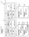
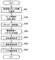
次に、図2に基づき、第2マイコン40のROM44のデータ更新について説明する。データ更新は、たとえばECU20の工場出荷時や、工場出荷後にディーラーなどで実行される。なお、更新するデータ、すなわち書き換えるプログラムは、ECU20が各種制御を実行するための制御プログラムなどである。本実施形態では、一例として、制御プログラムを書き換える。図2では、第1マイコン30を第1MC、第2マイコン40を第2MCとも示す。 Next, the data update of the
図2に示すように、第1マイコン30は、書換装置60から第2マイコン40のROM44の書換可能領域44aに記憶されている制御ログラムのリプロ要求(書換要求)を受信すると、上記したフラグを異常値にセットする。そして、第1マイコン30は、セットが完了したことを示す応答信号を、書換装置60に送信する。 As shown in FIG. 2, when the
次いで、第1マイコン30が、書換装置60から第2マイコン40への消去コマンドを受信及びROM44のデータを消去するアドレスデータを受信すると、消去コマンド及びアドレスデータを第2マイコン40に転送する。第2マイコン40は、消去コマンドを受信すると、CPU43にて実行する書換プログラムにより、書換可能領域44aにおけるアドレスデータに従う領域内のデータを消去する。データが消去された領域は、データ書き込み可能な状態となる。消去処理が終了すると、第2マイコン40は、消去処理終了を示す応答信号を第1マイコン30に送信し、第1マイコン30は、この応答信号を書換装置60に転送する。 Next, when the
次いで、第1マイコン30が、書換装置60から第2マイコン40への書込コマンド及び書込データを受信すると、書込コマンド及び書込データを第2マイコン40に転送する。第1マイコン30は、受信した書込データ内の所定アドレスに格納されている基準値を抽出する。第1マイコン30は、書込データを受信しながら基準値を抽出する。 Next, when the
本実施形態では、ECU20を安価に構成するために、第2マイコン40として第1マイコン30よりも不揮発性メモリ(ROM44)の容量が小さく、受信処理能力が低い安価なマイコンを用いている。したがって、書換装置60と第1マイコン30との間に一度に送受信可能なデータ量に対して、第1マイコン30と第2マイコン40との間で一度に送受信可能なデータ量が小さい。このため、第1マイコン30は、受信したデータを一旦RAM35に保存し、第2マイコン40が一度に受信可能なデータ量に分割して送信する。 In the present embodiment, in order to configure the
第2マイコン40は、書込コマンドを受信すると、その後送られてくる書込データを、ROM44の書換可能領域44a内において、データ消去によりデータ書き込み可能な状態となった領域に書き込み、ROM44が記憶するデータ(制御プログラム)を更新する。 When the
受信分の書込処理が終了すると、第2マイコン40は、書込処理終了を示す応答信号を第1マイコン30に送信し、第1マイコン30は、この応答信号を書換装置60に転送する。 When the writing process for the reception is completed, the
次いで、第1マイコン30は、書換装置60からROM44に書き込まれた書込データを読み出すための読出コマンドを受信すると、この読出コマンドを第2マイコン40に転送する。第2マイコン40は、読出コマンドを受信すると、先の書込処理によって書換可能領域44aに書き込んだ書込データを読み出して、第1マイコン30に送信する。以下においては、第2マイコン40から第1マイコン30へ送信する書込データを、読出データと示す。 Next, when the
第1マイコン30は読出データを受信しながら、予め設定された所定の演算を実行し、演算結果をRAM35に保存する。第1マイコン30は、後述するように、読出データに基準値が含まれていると、この基準値を除外して演算を実行する。そして、第2マイコン40から送信された読出データについて演算が終了すると、終了を示す応答信号を書換装置60に送信する。本実施形態では、図2に示すように、所定バイト単位、たとえば第2マイコン40が一括消去できるブロック単位(一例として16kバイト)で、上記した書き込み及び読み出しを繰り返す。したがって、最終的には、演算結果が、基準値を除くすべての読出データを用いたものとなる。 The
すべての書込データについてデータの書き込み及び読み出しが完了すると、書換装置60は、第1マイコン30に対して、不正確認コマンドを送信する。不正確認コマンドは、先に書き込まれた書込データが、不正に書き込まれたデータであったか否か、すなわちROM44のデータが不正に改ざんされたか否かの確認を指示するチェックコマンドである。不正確認コマンドは、ベリファイコマンドとも称される。 When the data writing and reading for all the write data are completed, the rewriting
第1マイコン30は、不正確認コマンドを受信すると、基準値と演算結果とに基づき、書込データが不正データか否かについて判定する判定処理を実行する。そして、判定結果に応じてフラグをセットし、判定結果、すなわちフラグのセット状態に応じた応答信号を、書換装置60に送信する。 When the
次に、図3〜図6に基づき、第2マイコン40のROM44のデータ更新に際して、第1マイコン30が実行する処理について説明する。第1マイコン30は、書換装置60から第2マイコン40のリプロ要求を受信すると、以下に示す処理を実行する。具体的には、第1マイコン30のCPU33が、ROM34の非書換領域34bに記憶されている書換プログラムに従って、処理を実行する。 Next, processing executed by the
書換装置60から、リプロ要求として、IDコードを含むデータが暗号化されて送信される。第1マイコン30は、通信回路31により受信したリプロ要求を復号し、非書換領域34bのアドレス情報領域34b1に記憶されている第2マイコン40のデータ更新用のIDコードと照合する。そして、照合の結果、一致する場合、図3に示すように、IDコードに関連付けられてアドレス情報領域34b1に記憶されている基準値のアドレス情報を、RAM35に設定(保存)する(ステップS100)。 From the
また、第1マイコン30は、書換可能領域34aのフラグ領域34a1に記憶されるフラグを異常値にセットする(ステップS200)。なお、ステップS100,S200の処理は、いずれを先に実行してもよい。たとえばフラグを異常値にセットした後に、アドレス情報をRAM35に設定してもよい。 Further, the
データの暗号化及び復号については、AES(Advanced Encryption Standard)などの共通鍵暗号アルゴリズムや公開鍵暗号アルゴリズムなどの周知技術を用いることができる。なお、リプロ要求に限らず、その他の各種コマンドや書込データも書換装置60にて暗号化されて送信され、第1マイコン30で復号される。以下において、暗号化及び復号に関する記載を省略する。 For data encryption and decryption, a known technique such as a common key encryption algorithm such as AES (Advanced Encryption Standard) or a public key encryption algorithm can be used. Not only the repro request but also various other commands and write data are encrypted and transmitted by the
ステップS100,S200の処理が終了すると、第1マイコン30は、フラグセットが完了したことを示す応答信号を、通信回路31を介して書換装置60に送信する(ステップS300)。ステップS300が終了すると、第1マイコン30は、消去通信処理を実行する(ステップS400)。図4は、第1マイコン30が実行する消去通信処理を示している。 When the processes of steps S100 and S200 are completed, the
図4に示すように、第1マイコン30は、通信回路31を介して第2マイコン40への消去コマンドを受信したか否かを判定する(ステップS402)。第1マイコン30は、消去コマンドを受信するまで待機する。 As shown in FIG. 4, the
第2マイコン40への消去コマンドを受信したと判定すると、第1マイコン30は、通信回路31を介して、データを消去するROM44のアドレスデータを受信する(ステップS404)。ステップS404では、第1マイコン30が、アドレスデータを受信するだけでなく、受信したアドレスデータを第2マイコン40用のアドレスデータに変換し、これをRAM35に保存することで、受信処理を終了する。 If it determines with having received the erase command to the
ステップS404の終了後、第1マイコン30は、受信した消去コマンドを、第2マイコン40が受付可能な第2マイコン40用の消去コマンドに変換し、通信回路32を介して第2マイコン40に送信する(ステップS406)。次いで第1マイコン30は、変換したアドレスデータを第2マイコン40に送信する(ステップS408)。アドレスデータについては、必要に応じて第2マイコン40が一度に受信可能なデータ量に分割し、通信回路32を介して第2マイコンに送信する。 After the end of step S404, the
ステップS408の終了後、第1マイコン30は、第2マイコン40の消去処理が終了したか否かを判定する(ステップS410)。第1マイコン30は、通信回路32を介して、第2マイコン40から消去処理終了を示す応答信号を受信するまで待機する。消去処理終了を示す応答信号を受信したと判定すると、第1マイコン30は次のステップS412の処理を実行する。第1マイコン30は、ステップS412において、第2マイコン40の消去処理が終了したことを示す応答信号を書換装置60に送信する。以上により、第1マイコン30は、消去通信処理を終了する。 After the end of step S408, the
図3に戻り、第1マイコン30は、ステップS400の消去通信処理が終了すると、次いで、書換通信処理を実行する(ステップS500)。図5は、第1マイコン30が実行する書換通信処理を示している。 Returning to FIG. 3, when the erasing communication process in step S400 is completed, the
図5に示すように、第1マイコン30は、通信回路31を介して第2マイコン40への書込コマンドを受信したか否かを判定する(ステップS502)。第1マイコン30は、書込コマンドを受信するまで待機する。 As shown in FIG. 5, the
書込コマンドを受信したと判定すると、第1マイコン30は、通信回路31を介して書込データを受信する(ステップS504)。ステップS504では、第1マイコン30が書込データを受信するだけでなく、受信した書込データを第2マイコン40が解釈可能な書込データに変換し、これをRAM35に保存することで、受信処理を終了する。 If it is determined that the write command has been received, the
上記したように、本実施形態では、第2マイコン40のデータを更新する際に、第1マイコン30が1回の処理で全書込データを受信するのではなく、所定バイト単位分の書込データを受信する。 As described above, in the present embodiment, when the data of the
第1マイコン30は、RAM35に設定されている基準値のアドレス情報(ステップS100参照)に基づき、書込データに所定アドレスのデータが含まれているか否か、すなわち所定アドレスのデータを受信したか否かを判定する(ステップS506)。第1マイコン30は、所定アドレスのデータを受信したと判定すると、当該アドレスの値を基準値としてRAM35に保存し(ステップS508)、次いでステップS510を実行する。ステップS506,508の処理については、書込データをRAM35に保存しつつ順に実行してもよいし、すべての書込データをRAM35に保存してから実行してもよい。なお、ステップS506,S508の処理が、抽出部に相当する。 Based on the reference value address information (see step S100) set in the
一方、受信した書込データが所定アドレスのものではないと判定した場合、ステップS508の処理を実行せずに、ステップS510の処理を実行する。ステップS510において、第1マイコン30は、通信回路32を介して第2マイコン40へ書込コマンドを送信する。このとき、第1マイコン30は、書込コマンドを、第2マイコン40が受付可能な書込コマンドに変換し、変換した書込コマンドを第2マイコン40へ送信する。 On the other hand, when it is determined that the received write data is not of the predetermined address, the process of step S510 is executed without executing the process of step S508. In step S <b> 510, the
次いで、第1マイコン30は、書込データを、第2マイコン40が一度に受信可能なデータ量に分割し、分割した書込データを通信回路32を介して順に第2マイコン40へ送信する(ステップS512)。第1マイコン30は、1回の送信で書換装置60から送信された分の書込データについて、書き込みが終了したか否かを判定する(ステップS514)。第1マイコン30は、書き込みが終了するまで待機する。第1マイコン30は、第2マイコン40から書込処理終了を示す応答信号を受信すると、書き込みが終了したと判定する。書込終了と判定すると、マイコン30は、通信回路31を介して書換装置60に、1回の送信分の書き込みが終了したことを示す応答信号を送信する(ステップ516)。 Next, the
次いで、第1マイコン30は、通信回路31を介して第2マイコン40への読出コマンドを受信したか否かを判定する(ステップS518)。第1マイコン30は、読出コマンドを受信するまで待機する。 Next, the
読出コマンドを受信すると、第1マイコン30は、読出コマンドを、第2マイコン40が受付可能な読出コマンドに変換し、変換した読出コマンドを第2マイコン40へ送信する(ステップS520)。そして、第2マイコン40から送信された読出データを受信する(ステップS522)。ステップS520,S522の処理が取得部に相当する。 When receiving the read command, the
次いで、第1マイコン30は、RAM35に設定されている基準値のアドレス情報に基づき、読出データに所定アドレスのデータが含まれているか否か、すなわち所定アドレスのデータを受信したか否かを判定する(ステップS524)。そして、所定アドレスのデータを受信したと判定した場合、当該アドレスの値が基準値であるとして、演算処理の対象から除外し(ステップS526)、予め設定された所定の演算を実行して演算結果をRAM35に保存する(ステップS528)。一方、読出データが所定アドレスのデータではない場合、ステップS526を実行せず、ステップS528を実行する。ステップS524,S526,S528の処理が、演算部に相当する。 Next, based on the reference value address information set in the
このように、所定アドレスに格納された値である基準値は演算に用いず、基準値以外のデータを演算に用いる。演算手法については特に限定されない。 As described above, the reference value that is the value stored at the predetermined address is not used for the calculation, and data other than the reference value is used for the calculation. The calculation method is not particularly limited.
次いで、第1マイコン30は、第2マイコン40から読み出した読出データについて演算が終了すると、演算終了を示す応答信号を書換装置60に送信する(ステップS530)。そして、第1マイコン30は、再び第2マイコン40への書込コマンドを受信したか否かを判定する(ステップS532)。書込コマンドを受信したと判定すると、ステップS504に戻り、ステップS504以降の処理を繰り返す。書換装置60から送信される書込データが残っている場合、ステップS532で書込コマンドを受信することとなる。 Next, when the calculation for the read data read from the
ステップS532で書込コマンドの受信なしと判定すると、第1マイコン30は、不正確認コマンドを受信したか否かを確認する(ステップS534)。そして、不正確認コマンドを受信したと判定すると、一連の処理を終了する。書換装置60から送信される書込データがなくなると、ステップS534で不正確認コマンドを受信することとなる。 If it is determined in step S532 that no write command has been received, the
一方、ステップS534で不正確認コマンドの受信なしと判定すると、ステップS532に戻る。すなわち、ステップS530の送信処理後、書込コマンド及び不正確認コマンドのいずれかを受信するまで、ステップS532,S534の処理を繰り返す。 On the other hand, if it is determined in step S534 that no fraud confirmation command has been received, the process returns to step S532. That is, after the transmission process in step S530, the processes in steps S532 and S534 are repeated until either the write command or the fraud confirmation command is received.
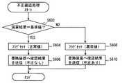
図3に戻り、第1マイコン30は、ステップS500の書換通信処理が終了すると、次いで、不正確認処理を実行する(ステップS600)。そして、不正確認処理の実行後、一連の処理を終了する。図6は、第1マイコン30が実行する不正確認処理を示している。 Returning to FIG. 3, when the rewrite communication process in step S500 is completed, the
第1マイコン30は、不正確認コマンドを受信すると、図6に示す不正確認処理を実行する。先ず第1マイコン30は、最終的にステップS528で得られた演算結果と、ステップS508でRAM35に保存した基準値とが、予め決定された所定の関係を満たすか否かを判定する。その一例として本実施形態では、第1マイコン30が、演算結果と基準値とが一致するか否かを判定する(ステップS602)。 When receiving the fraud confirmation command, the
ステップS602で一致と判定すると、第1マイコン30は、フラグ領域34a1に記憶されるフラグを正常値にセットする(ステップS604)。そして、第1マイコン30は、書換装置60へ不正データの書き込みなし、すなわち第三者によるデータ改ざんなしを示す確認結果を送信し(ステップS606)、一連の処理を終了する。 If it is determined in step S602 that they match, the
一方、ステップS602で一致せずと判定すると、第1マイコン30は、フラグ領域34a1に記憶されるフラグを異常値のまま維持する(ステップS608)。換言すれば、フラグを異常時に再びセットする。そして、第1マイコン30は、書換装置60へ不正データの書き込みあり、すなわち第三者によるデータ改ざんありを示す確認結果を送信し(ステップS610)、一連の処理を終了する。 On the other hand, if it is determined in step S602 that they do not match, the
なお、ステップS602に示す処理が、判定部に相当する。ステップS606,S610に示す処理が、通知部に相当する。ステップS200,S604,S608に示す処理が、フラグ状態設定部に相当する。 Note that the process shown in step S602 corresponds to a determination unit. The processing shown in steps S606 and S610 corresponds to a notification unit. The processes shown in steps S200, S604, and S608 correspond to a flag state setting unit.
次に、図7に基づき、第2マイコン40のROM44のデータ更新に際して、書換装置60が実行する処理について説明する。 Next, a process executed by the rewriting
書換装置60は、先ず、第1マイコン30に対して、第2マイコン40のリプロ要求を送信する(ステップS700)。このリプロ要求として、上記したように、第2マイコン40のデータ更新用のIDコードを含むデータが暗号化されて送信される。 The rewriting
次いで、書換装置60は、第1マイコン30のフラグが異常値にセットされたか否かを判定する(ステップS702)。書換装置60は、フラグが異常値にセットされたと判定するまで待機する。書換装置60は、第1マイコン30から、異常値へのセット完了を示す応答信号を受信すると、フラグセット済みと判定する。 Next, the rewriting
次いで、書換装置60は、第1マイコン30に対して、第2マイコン40への消去コマンドを送信し(ステップS704)、送信後は、第2マイコン40の消去処理が終了したか否かを判定する(ステップS706)。書換装置60は、第1マイコン30から、第2マイコン40の消去処理終了を示す応答信号を受信するまで待機する。 Next, the rewriting
ステップS706において消去処理終了と判定すると、書換装置60は、第1マイコン30に対して、第2マイコン40への書込コマンドを送信し(ステップS708)、次いで書込データを送信する(ステップS710)。上記したように、書換装置60は、1回の書込コマンドにつき、所定バイト分の書込データを送信する。 When it is determined in step S706 that the erasing process is completed, the rewriting
次いで、書換装置60は、送信分の書込データの書込処理が終了したか否かを判定する(ステップS712)。書換装置60は、第1マイコン30から、第2マイコン40の書込終了を示す応答信号を受信するまで待機する。ステップS712で書込処理が終了していると判定すると、書換装置60は、第2マイコン40への読出コマンドを送信する(ステップS714)。 Next, the rewriting
そして、書換装置60は、第2マイコン40のROM44のデータ更新に際して、すべての書込データの送信が終了したか否かを判定する(ステップS716)。ステップS716で、全書込データの送信が終了していないと判定すると、書換装置60は、ステップS708に戻り、残りの書込データについて、ステップS708以降の処理を実行する。書換装置60は、第1マイコン30から演算終了を示す応答信号(ステップS530参照)を受信したときに、書込データの送信に残りがある場合、全書込データの送信が終了していないと判定し、応答信号を受信したときに書込データに残りがないと、全書込データの送信が終了したと判定する。 Then, the
ステップS716で、全書込データの送信が終了したと判定すると、次いで書換装置60は、第1マイコン30に対し、不正確認コマンドを送信する(ステップS718)。そして、書換装置60は、第1マイコン30の判定結果を受信し(ステップS720)、判定結果に関して、ECU20の外部に通知する通知処理を実行する(ステップS722)。以上により、一連の処理を終了する。 If it is determined in step S716 that the transmission of all the write data has been completed, then the
なお、通知処理としては、たとえば車両のモニタに不正データの書き込みがなされたことを表示させるなどが考えられる。これによれば、ユーザに対して、書換装置60を用いた第2マイコン40のROM44のデータ更新の再度の実行を促すことができる。 As the notification process, for example, it may be possible to display that illegal data has been written on the vehicle monitor. According to this, it is possible to prompt the user to execute again the data update of the
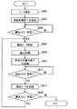
次に、図8に基づき、第2マイコン40のROM44のデータ更新に際して、第2マイコン40が実行する処理について説明する。第2マイコン40は、消去コマンド及びアドレスデータを受信すると、以下に示す処理を実行する。具体的には、第2マイコン40のCPU43が、ROM44の非書換領域44bに記憶されている書換プログラムに従って、処理を実行する。 Next, a process executed by the
消去コマンド及びアドレスデータを受信すると、図8に示すように、第2マイコン40は、書換可能領域44aにおけるアドレスデータに従う領域内のデータを消去する(ステップS800)。データが消去された領域は、データ書き込み可能な状態となる。消去処理が終了すると、第2マイコン40は、消去処理終了を示す応答信号を第1マイコン30に送信する(ステップS802)。 When the erase command and the address data are received, as shown in FIG. 8, the
次いで第2マイコン40は、第1マイコン30から書込コマンドを受信したか否かを判定する(ステップS804)。第2マイコン40は、書込コマンドを受信するまで待機する。書込コマンドの受信後、第2マイコン40は、第1マイコン30から書込データを受信し(ステップS806)、データが消去された領域に書込データの書込処理を実行する(ステップS808)。 Next, the
第2マイコン40は、受信分の書込データの書き込みが終了すると、書込終了を示す応答信号を第1マイコン30に送信する(ステップS810)。応答信号の送信後、第2マイコン40は、第1マイコン30から読出コマンドを受信したか否かを判定する(ステップS812)。第2マイコン40は、読出コマンドを受信するまで待機する。 When the writing of the received write data is completed, the
読出コマンドを受信したと判定すると、第2マイコン40は、ROM44の書換可能領域44aに書き込んだ書込データを読み出し、読出データとして第1マイコン30に送信する(ステップS814)。第2マイコン40は、読出データの送信から予め設定された所定時間の間に、書込コマンドを再び受信するか否かを判定する(ステップS816)。書込コマンドを受信したと判定すると、ステップS806に戻り、ステップS806以降の処理を実行する。書込データが残っている場合には、ステップS816で書込コマンドを受信することとなる。 If it is determined that the read command has been received, the
一方、すべての書込データについての書き込み及び読み出しが終了している場合、ステップS816で書込コマンドを受信することはなく、一連の処理は終了となる。 On the other hand, if writing and reading for all the write data have been completed, the write command is not received in step S816, and the series of processing ends.
次に、上記したECU20及びデータ書換システム10の効果について説明する。 Next, effects of the
書込データとして、第三者により不正データが書き込まれた場合、書込データ内の所定アドレスには基準値が格納されていない。よって、アドレス情報により第1マイコン30が抽出した基準値と、基準値を除く書込データによる演算結果との関係が、所定の関係を満たすことはない。 When illegal data is written as write data by a third party, a reference value is not stored at a predetermined address in the write data. Therefore, the relationship between the reference value extracted by the
一方、書換装置60により正規の書込データが書き込まれた場合、書込データ内の所定アドレスには基準値が格納されている。よって、アドレス情報により第1マイコン30が抽出した基準値と、基準値を除く書込データによる演算結果との関係が、所定の関係を満たす。 On the other hand, when regular write data is written by the rewriting
このように本実施形態によれば、基準値と演算結果との判定結果に基づき、書込データが正規に書き込まれたデータであるか、それとも不正データであるのかを判定することができる。すなわち、書込データが第1マイコン30により転送されて第2マイコン40のROM44(外部メモリ)に書き込まれ、ROM44のデータが更新されるECU20及びデータ書換システム10において、第三者による不正データの書き込み、すなわちデータ改ざんを検出することができる。 As described above, according to this embodiment, it is possible to determine whether the write data is data that has been written normally or illegal data based on the determination result between the reference value and the calculation result. That is, write data is transferred by the
なお、不正データの書き込みのみならず、ノイズ重畳により、第1マイコン30と第2マイコン40との通信過程でエラーが生じた場合にも、基準値と演算結果とが所定の関係を満たさなくなる。したがって、通信過程でのエラーも検出することができる。 Note that the reference value and the calculation result do not satisfy the predetermined relationship not only when the illegal data is written but also when an error occurs in the communication process between the
また、本実施形態では、基準値のアドレス情報が、第1マイコン30のROM34における非書換領域34b(アドレス情報領域34b1)に予め記憶されている。よって、基準値のアドレス情報を、第1マイコン30の外部から取得する構成に較べて、基準値及びアドレス情報が外部に第三者の手に渡りにくく、セキュリティ性を向上することができる。 In the present embodiment, reference value address information is stored in advance in a
また、本実施形態では、第1マイコン30のROM34のうち、書換可能領域34aにフラグ領域34a1を設け、フラグ領域34a1に、正規データの書き込みが完了したか否かを管理するフラグを記憶されている。そして、第1マイコン30は、書込データを第2マイコン40に送信する前に、敢えてフラグを異常状態に設定し、基準値と演算結果との判定の結果、所定の関係を満たす場合にのみフラグを正常状態に設定しなおす。一方、所定の関係を満たさない場合、フラグを異常状態に維持する。このように、フラグを用いることで、フラグ情報をROM44に格納することが厳しい第2マイコン40を用いる場合でも、不正データの確認を容易に行うことができる。また、途中で処理が止まっても、フラグの状態を確認することができる。 In the present embodiment, in the ROM 34 of the
(第2実施形態)
本実施形態は、先行実施形態を参照できる。このため、先行実施形態に示したECU20及びデータ書換システム10と共通する部分についての説明は省略する。(Second Embodiment)
This embodiment can refer to the preceding embodiment. For this reason, the description about the part which is common in ECU20 and the
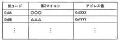
たとえば、要求される機能に応じて、複数の第2マイコン40の中からひとつを選択し、ECU20に搭載することが考えられる。このため、本実施形態では、非書換領域34bのアドレス情報領域34b1に、図9に示すように、複数のアドレス情報が記憶されている。具体的には、ECU20として搭載可能な複数の第2マイコン40分の基準値のアドレス情報が記憶されている。 For example, it is conceivable that one of the plurality of
本実施形態でも、書換装置60から、リプロ要求として、IDコードを含むデータが暗号化されて送信される。また、図9に示すように、第2マイコン40の種類に応じてIDコードが設定されている。したがって、第1マイコン30は、リプロ要求を受信すると、図10に示すように、リプロ要求として受信したデータのIDコードに基づいて、搭載されている第2マイコン40の種類、すなわち対応する基準値のアドレス情報を選択する(ステップS90)。このステップS90に示す処理が、選択部に相当する。 Also in this embodiment, the data including the ID code is encrypted and transmitted from the rewriting
ステップS90の実行後、第1マイコン30は、ステップS100を実行する。すなわち、ステップS90で選択した基準値のアドレス情報を、RAM35に設定する。以下の処理は第1実施形態と同じである。 After execution of step S90, the
本実施形態によれば、第2マイコン40を変更しても、共通する第1マイコン30にて、不正データの書き込み検出を実行することができる。 According to the present embodiment, even if the
(第3実施形態)
本実施形態は、先行実施形態を参照できる。このため、先行実施形態に示したECU20及びデータ書換システム10と共通する部分についての説明は省略する。(Third embodiment)
This embodiment can refer to the preceding embodiment. For this reason, the description about the part which is common in ECU20 and the
先行実施形態では、第1マイコン30が有するROM34の非書換領域34b(アドレス情報領域34b1)に、基準値のアドレス情報が予め記憶されている例を示した。これに対し、本実施形態では、書換装置60がリプロ要求として、IDコードに加えて基準値のアドレス情報も送信する。 In the preceding embodiment, the example in which the reference value address information is stored in advance in the
このため、第1マイコン30は、リプロ要求として、基準値のアドレス情報を受信する。そして、図11に示すように、受信した基準値のアドレス情報を、RAM35に設定する(ステップS110)。それ以後の処理については第1実施形態と同じである。ステップS110に示す処理が、設定部に相当する。 For this reason, the
これによれば、ROM44の容量や基準値の格納されるアドレスに変更が生じた場合にも、不正データの書き込み検出を実施することができる。すなわち、設計の自由度を向上することができる。また、ROM34に、予め基準値のアドレス情報を記憶させておく必要がない。 According to this, even when there is a change in the capacity of the
上記実施形態の構造は、あくまで例示であって、本発明の範囲はこれらの記載の範囲に限定されるものではない。本発明の範囲は、特許請求の範囲の記載によって示され、さらに特許請求の範囲の記載と均等の意味及び範囲内でのすべての変更を含むものである。 The structure of the said embodiment is an illustration to the last, Comprising: The scope of the present invention is not limited to the range of these description. The scope of the present invention is indicated by the description of the scope of claims, and further includes meanings equivalent to the description of the scope of claims and all modifications within the scope.
上記実施形態では、外部メモリとして、第2マイコン40のROM44の例を示したが
これに限定されるものではない。外部メモリとしては、第1マイコン30(マイコン)の外部に設けられ、書換可能な不揮発性のメモリであれば採用することができる。In the above embodiment, the example of the
上記実施形態では、第2マイコン40のROM44のデータ(制御プログラム)を更新する際に、所定バイト単位で書き込み及び読み出しを実行する例を示した。しかしながら、更新するためのすべての書込データを1回の書込コマンドで第1マイコン30に送信し、1回の読出コマンドですべての読出データを第1マイコン30に送信する構成を採用することもできる。この場合、図5に示したステップS530が不要となる。 In the above-described embodiment, an example in which writing and reading are performed in units of a predetermined byte when updating data (control program) in the
フラグを用いる例を示したが、フラグのない構成を採用することもできる。 Although an example using a flag has been shown, a configuration without a flag may be employed.
10…データ書換システム、20…電子制御装置(ECU)、30…第1マイコン、31,32…通信回路、33…CPU、34…ROM、34a…書換可能領域、34a1…フラグ領域、34b…非書換領域、34b1…アドレス情報領域、40…第2マイコン、41…通信回路、43…CPU、44…ROM、44a…書換可能領域、44b…非書換領域、45…RAM、50…外部通信線、51…内部通信線、60…書換装置DESCRIPTION OF
Claims (5)
Translated fromJapanese書換装置(60)から送信された書込データが前記マイコンにより転送されて前記外部メモリに書き込まれ、前記外部メモリのデータが更新される電子制御装置であって、
前記マイコンが、前記書込データが不正データであるか否かを判定するための基準値を、受信した前記書込データ内の所定アドレスから抽出する抽出部(S506,S508)と、前記外部メモリに書き込まれた前記書込データを、前記外部メモリから取得する取得部(S520,S522)と、前記取得部が取得した前記書込データのうち、前記基準値を除くデータを用いて、所定の演算を実行する演算部(S524,S526,S528)と、前記演算部による演算結果と前記基準値との関係が、予め設定された所定の関係を満たすか否かを判定する判定部(S602)と、前記判定部の判定結果を前記書換装置に送信する通知部(S606,S610)と、を有し、
前記マイコンは、書換可能な不揮発性メモリ(34)を有し、
前記基準値のアドレス情報は、前記不揮発性メモリにおいてデータの書き換えが不可能な非書換領域(34b)に予め記憶されている電子制御装置。A microcomputer (30) and a rewritable nonvolatile external memory (44) provided outside the microcomputer;
An electronic control device in which write data transmitted from a rewrite device (60) is transferred by the microcomputer and written to the external memory, and data in the external memory is updated,
An extracting unit (S506, S508) for extracting a reference value for determining whether or not the write data is illegal data from a predetermined address in the received write data; and the external memory The acquisition unit (S520, S522) that acquires the write data written in the external memory, and the write data acquired by the acquisition unit using data excluding the reference value, A calculation unit (S524, S526, S528) that executes a calculation, and a determination unit that determines whether or not the relationship between the calculation result by the calculation unit and the reference value satisfies a predetermined relationship (S602). If,possess the notification unit of the determination result of the determination unit is transmitted to the rewriting device and (S606, S610),and
The microcomputer has a rewritable nonvolatile memory (34),
The electronic control devicein which the address information of the reference value is stored in advance in a non-rewritable area (34b) where data cannot be rewritten in the nonvolatile memory .
前記マイコンは、前記書換装置から送信された情報に基づいて、前記複数のアドレス情報の中からひとつを選択する選択部(S90)を有し、
前記抽出部は、選択された前記アドレス情報に基づいて前記基準値を抽出する請求項1に記載の電子制御装置。In the non-rewritable area, a plurality of address information is stored in advance,
The microcomputer has a selection unit (S90) for selecting one of the plurality of address information based on the information transmitted from the rewriting device,
The electronic control device according toclaim 1 , wherein the extraction unit extracts the reference value based on the selected address information.
書換装置(60)から送信された書込データが前記マイコンにより転送されて前記外部メモリに書き込まれ、前記外部メモリのデータが更新される電子制御装置であって、
前記マイコンが、前記書込データが不正データであるか否かを判定するための基準値を、受信した前記書込データ内の所定アドレスから抽出する抽出部(S506,S508)と、前記外部メモリに書き込まれた前記書込データを、前記外部メモリから取得する取得部(S520,S522)と、前記取得部が取得した前記書込データのうち、前記基準値を除くデータを用いて、所定の演算を実行する演算部(S524,S526,S528)と、前記演算部による演算結果と前記基準値との関係が、予め設定された所定の関係を満たすか否かを判定する判定部(S602)と、前記判定部の判定結果を前記書換装置に送信する通知部(S606,S610)と、を有し、
前記マイコンは、前記書換装置から送信された情報を、前記基準値のアドレス情報として設定する設定部(S110)を有し、
前記抽出部は、設定された前記アドレス情報に基づいて前記基準値を抽出する電子制御装置。A microcomputer (30) and a rewritable nonvolatile external memory (44) provided outside the microcomputer;
An electronic control device in which write data transmitted from a rewrite device (60) is transferred by the microcomputer and written to the external memory, and data in the external memory is updated,
An extracting unit (S506, S508) for extracting a reference value for determining whether or not the write data is illegal data from a predetermined address in the received write data; and the external memory The acquisition unit (S520, S522) that acquires the write data written in the external memory, and the write data acquired by the acquisition unit using data excluding the reference value, A calculation unit (S524, S526, S528) that executes a calculation, and a determination unit that determines whether or not the relationship between the calculation result by the calculation unit and the reference value satisfies a predetermined relationship (S602). If,possess the notification unit of the determination result of the determination unit is transmitted to the rewriting device and (S606, S610),and
The microcomputer has a setting unit (S110) for setting information transmitted from the rewriting device as address information of the reference value,
The extraction unit is an electronic control devicethat extracts the reference value based on the set address information .
前記第1マイコンとは別に設けられた第2マイコン(40)をさらに備え、
前記第2マイコンに、前記外部メモリが内蔵されている請求項1〜4いずれか1項に記載の電子制御装置。The microcomputer is a first microcomputer;
A second microcomputer (40) provided separately from the first microcomputer;
The electronic control device according toclaim 1 , wherein the external memory is built in the second microcomputer.
Priority Applications (2)
| Application Number | Priority Date | Filing Date | Title |
|---|---|---|---|
| JP2015217816AJP6468168B2 (en) | 2015-11-05 | 2015-11-05 | Electronic control unit |
| DE102016221667.8ADE102016221667B4 (en) | 2015-11-05 | 2016-11-04 | Electronic control unit and data rewriting system |
Applications Claiming Priority (1)
| Application Number | Priority Date | Filing Date | Title |
|---|---|---|---|
| JP2015217816AJP6468168B2 (en) | 2015-11-05 | 2015-11-05 | Electronic control unit |
Publications (2)
| Publication Number | Publication Date |
|---|---|
| JP2017091057A JP2017091057A (en) | 2017-05-25 |
| JP6468168B2true JP6468168B2 (en) | 2019-02-13 |
Family
ID=58585312
Family Applications (1)
| Application Number | Title | Priority Date | Filing Date |
|---|---|---|---|
| JP2015217816AActiveJP6468168B2 (en) | 2015-11-05 | 2015-11-05 | Electronic control unit |
Country Status (2)
| Country | Link |
|---|---|
| JP (1) | JP6468168B2 (en) |
| DE (1) | DE102016221667B4 (en) |
Families Citing this family (3)
| Publication number | Priority date | Publication date | Assignee | Title |
|---|---|---|---|---|
| JP6898643B2 (en)* | 2017-08-10 | 2021-07-07 | 株式会社Subaru | Electronic control device for vehicles |
| JP7731690B2 (en)* | 2021-04-14 | 2025-09-01 | Astemo株式会社 | Control device and control system |
| JP7524939B2 (en)* | 2022-01-12 | 2024-07-30 | トヨタ自動車株式会社 | System, program update confirmation method and update confirmation program |
Family Cites Families (8)
| Publication number | Priority date | Publication date | Assignee | Title |
|---|---|---|---|---|
| JP2000200193A (en)* | 1999-01-06 | 2000-07-18 | Toshiba Tec Corp | Data processing device |
| US6725323B2 (en) | 2001-12-06 | 2004-04-20 | Kabushiki Kaisha Toshiba | Apparatus and method for updating flash ROM in an electronic apparatus having a plurality of boards |
| JP2004030539A (en)* | 2002-06-28 | 2004-01-29 | Sony Corp | Information processing apparatus and method, recording medium, and program |
| JP2005178169A (en)* | 2003-12-19 | 2005-07-07 | Canon Inc | Printing device |
| JP2005275843A (en)* | 2004-03-25 | 2005-10-06 | Murata Mach Ltd | Data processor |
| JP2006268107A (en) | 2005-03-22 | 2006-10-05 | Denso Corp | Electronic controller |
| JP2008040924A (en)* | 2006-08-09 | 2008-02-21 | Murata Mach Ltd | Firmware rewriting method and firmware reading method |
| JP5744078B2 (en)* | 2013-01-31 | 2015-07-01 | Necプラットフォームズ株式会社 | Embedded device control system, embedded device control device, and control method of embedded device control device |
- 2015
- 2015-11-05JPJP2015217816Apatent/JP6468168B2/enactiveActive
- 2016
- 2016-11-04DEDE102016221667.8Apatent/DE102016221667B4/enactiveActive
Also Published As
| Publication number | Publication date |
|---|---|
| DE102016221667B4 (en) | 2024-12-19 |
| JP2017091057A (en) | 2017-05-25 |
| DE102016221667A1 (en) | 2017-05-11 |
Similar Documents
| Publication | Publication Date | Title |
|---|---|---|
| US10013365B2 (en) | Method for programming a control unit of a motor vehicle | |
| CN110178114B (en) | Vehicle control device and program update system | |
| JP5411122B2 (en) | Information processing device | |
| CN103198270B (en) | Inventory is used to record the existence of effective software and calibration file | |
| JP6468168B2 (en) | Electronic control unit | |
| CN114844874A (en) | OTA manager, update control method, non-transitory storage medium, and vehicle | |
| JP6354566B2 (en) | Microcomputer | |
| JP2013026964A (en) | Information update device for vehicle and information update method for vehicle | |
| KR20170102285A (en) | Security Elements | |
| WO2020090418A1 (en) | Electronic control device, and reprogramming method for electronic control device | |
| JP6895373B2 (en) | Electronic control device for automobiles | |
| CN109983462B (en) | Information processing apparatus and information processing method | |
| JP7087334B2 (en) | Electronic control device | |
| JP7408593B2 (en) | Control devices, information processing devices, and information processing systems | |
| US20050034034A1 (en) | Control device with rewriteable control data | |
| JP6610060B2 (en) | Relay device, program, and information processing system | |
| JP7211189B2 (en) | Update processing system and update processing method | |
| JP5358599B2 (en) | Software rewriting device and software rewriting method using the device | |
| JP5226383B2 (en) | Microcomputer identification information management system and method | |
| JP6107710B2 (en) | Program management device, vehicle control device, and program management program | |
| JP2015140038A (en) | On-vehicle control device | |
| CN120787343A (en) | Apparatus and method for providing protected data, microcontroller system and sensor system | |
| JP2007015643A (en) | Electronic control device for vehicle | |
| JP4661244B2 (en) | Air conditioner | |
| JP2018205896A (en) | Software management system |
Legal Events
| Date | Code | Title | Description |
|---|---|---|---|
| A621 | Written request for application examination | Free format text:JAPANESE INTERMEDIATE CODE: A621 Effective date:20180209 | |
| A977 | Report on retrieval | Free format text:JAPANESE INTERMEDIATE CODE: A971007 Effective date:20181017 | |
| A131 | Notification of reasons for refusal | Free format text:JAPANESE INTERMEDIATE CODE: A131 Effective date:20181023 | |
| A521 | Request for written amendment filed | Free format text:JAPANESE INTERMEDIATE CODE: A523 Effective date:20181128 | |
| TRDD | Decision of grant or rejection written | ||
| A01 | Written decision to grant a patent or to grant a registration (utility model) | Free format text:JAPANESE INTERMEDIATE CODE: A01 Effective date:20181218 | |
| A61 | First payment of annual fees (during grant procedure) | Free format text:JAPANESE INTERMEDIATE CODE: A61 Effective date:20181231 | |
| R151 | Written notification of patent or utility model registration | Ref document number:6468168 Country of ref document:JP Free format text:JAPANESE INTERMEDIATE CODE: R151 | |
| R250 | Receipt of annual fees | Free format text:JAPANESE INTERMEDIATE CODE: R250 | |
| R250 | Receipt of annual fees | Free format text:JAPANESE INTERMEDIATE CODE: R250 | |
| R250 | Receipt of annual fees | Free format text:JAPANESE INTERMEDIATE CODE: R250 | |
| R250 | Receipt of annual fees | Free format text:JAPANESE INTERMEDIATE CODE: R250 |