JP6464064B2 - Charged particle equipment - Google Patents
Charged particle equipmentDownload PDFInfo
- Publication number
- JP6464064B2 JP6464064B2JP2015175938AJP2015175938AJP6464064B2JP 6464064 B2JP6464064 B2JP 6464064B2JP 2015175938 AJP2015175938 AJP 2015175938AJP 2015175938 AJP2015175938 AJP 2015175938AJP 6464064 B2JP6464064 B2JP 6464064B2
- Authority
- JP
- Japan
- Prior art keywords
- sample
- charged particles
- charged particle
- deflector
- detector
- Prior art date
- Legal status (The legal status is an assumption and is not a legal conclusion. Google has not performed a legal analysis and makes no representation as to the accuracy of the status listed.)
- Active
Links
Images


Description
Translated fromJapanese本発明は、荷電粒子装置に関する。 The present invention relates to a charged particle device.
透過電子顕微鏡(TEM)では、透過像(試料像)や、回折パターンを取得することができる(例えば特許文献1参照)。透過像は試料を透過した電子(透過電子)で結像された像であり、回折パターンは電子回折により得られる図形である。 With a transmission electron microscope (TEM), a transmission image (sample image) and a diffraction pattern can be acquired (see, for example, Patent Document 1). The transmission image is an image formed by electrons transmitted through the sample (transmission electrons), and the diffraction pattern is a figure obtained by electron diffraction.
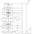
図10は、従来の透過電子顕微鏡1000の構成を模式的に示す図である。 FIG. 10 is a diagram schematically showing a configuration of a conventional
図10に示すように、透過電子顕微鏡1000は、電子源1002と、電子源1002からの電子を試料に照射する照射光学系1004と、試料を保持する試料ステージ1006と、試料を透過した電子を用いて最初に結像する対物レンズ1008と、対物レンズ1008で結像された透過像または回折パターンを検出面上に結像する結像光学系1010と、検出面に入射した電子を検出して透過像または回折パターンを取得する検出器1012と、これらを制御する制御部1020と、を備えている。 As shown in FIG. 10, a
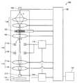
図11は、結像光学系1010がMAGモードの状態を模式的に示す図である。図12は、結像光学系1010がDIFFモードの状態を模式的に示す図である。 FIG. 11 is a diagram schematically showing a state in which the imaging
透過電子顕微鏡1000で試料の透過像を取得する場合、ユーザーは、試料の透過像を観察しながら試料を探索する。このとき、透過電子顕微鏡1000の結像光学系1010の条件は、図11に示すように、対物レンズ1008が生成する最初の像を検出面上に結像する条件(MAGモード)となっている。 When acquiring a transmission image of a sample with the
そして、所望の観察領域が見つかると、ユーザーは、必要に応じて制御部1020を操作して結像光学系1010の条件を切り替えて倍率を調整し、検出器で透過像を取得する。 When a desired observation region is found, the user operates the
通常、透過像のみでは、試料の構造を示す情報としては足りない場合が多い。透過電子顕微鏡1000では、試料で散乱した電子は、対物レンズ1008の後焦点面に回折パターンを形成している。そこで、結像光学系1010の条件を変えて、図12に示すように、回折パターンを検出面上に結像する条件(DIFFモード)にする。ユーザーは結像光学系1010の条件を変えて、回折パターンの拡大率(カメラ長)を調整し、検出器で回折パターンを取得する。 Usually, the transmission image alone is often insufficient as information indicating the structure of the sample. In the
上述したように、透過電子顕微鏡では、透過像(実空間像)と回折パターン(逆空間像)の両方を取得することができる。 As described above, the transmission electron microscope can acquire both a transmission image (real space image) and a diffraction pattern (reverse space image).
しかしながら、透過像を検出面上に結像する結像光学系の条件と、回折パターンを検出面上に結像する結像光学系の条件とは、大きく異なる。したがって、1つの試料から透過
像と回折パターンを取得する場合は、必ず結像光学系の条件を変える必要がある。However, the conditions of the imaging optical system that forms the transmission image on the detection surface are significantly different from the conditions of the imaging optical system that forms the diffraction pattern on the detection surface. Accordingly, when acquiring a transmission image and a diffraction pattern from one sample, it is necessary to change the conditions of the imaging optical system.
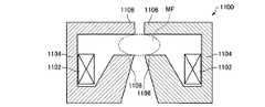
図13は、結像光学系を構成している、一般的な磁場レンズ1100を模式的に示す図である。 FIG. 13 is a diagram schematically showing a general
電子を結像するために用いられる磁場レンズ1100は、図13に示すように、コイル1102と、ヨーク1104と、ポールピース1106と、を有している。磁場レンズ1100では、コイル1102に電流を流し、コイル1102で発生した磁場をヨーク1104を介してポールピース1106に集めることで磁場MFを発生させる。磁場レンズ1100では、コイル1102に流れる電流を調整することで磁場MFをコントロールすることができる。磁場レンズ1100は、磁場MFによって電子の軌道を変更し、レンズとして機能する。 As shown in FIG. 13, the
ヨーク1104およびポールピース1106は、磁性体で構成されている。ヨーク1104およびポールピース1106を構成する磁性体には、磁気ヒステリシスが存在する。 The
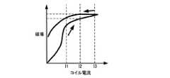
図14は、磁場レンズの磁気ヒステリシスを説明するためのグラフである。図14に示すグラフの横軸は、磁場レンズのコイルに流れる電流量であり、縦軸は磁場レンズが発生させる磁場の大きさである。 FIG. 14 is a graph for explaining the magnetic hysteresis of the magnetic lens. The horizontal axis of the graph shown in FIG. 14 is the amount of current flowing through the coil of the magnetic lens, and the vertical axis is the magnitude of the magnetic field generated by the magnetic lens.
図14に示すように、コイル電流量がI1の状態からコイル電流量を増加させてコイル電流量をI2にした場合と、コイル電流量がI3の状態からコイル電流量を減少させてコイル電流量をI2にした場合では、コイル励磁量が同じI2であっても、磁場の大きさ(レンズ強度)は異なっている。 As shown in FIG. 14, when the coil current amount is increased from the state where the coil current amount is I1 and the coil current amount is set to I2, and when the coil current amount is decreased from the state where the coil current amount is I3, the coil current amount is decreased. When I2 is I2, the magnitude of the magnetic field (lens strength) is different even if the coil excitation amount is the same I2.
したがって、透過電子顕微鏡において、結像光学系の条件を変えると、変える前の結像光学系の条件によって、同じ条件であっても結像光学系が実現している結像状態(倍率や、カメラ長)が変わってしまう。 Therefore, in the transmission electron microscope, when the conditions of the imaging optical system are changed, depending on the conditions of the imaging optical system before the change, the imaging state (magnification, Camera length) will change.
また、図13に示すコイル1102に電流を流すことで、コイル1102からジュール熱が発生する。このジュール熱によって、ヨーク1104およびポールピース1106が膨張する。コイル1102を流れる電流が一定であれば熱的平衡状態にあるため、特に大きな問題とならない。しかしながら、コイル1102を流れる電流を変化させると、熱的変化が発生して、ヨーク1104およびポールピース1106の形状の変化が起こる。これにより、磁場レンズ1100が発生させる磁場MFの形状も変わる。 In addition, Joule heat is generated from the
したがって、結像光学系の条件を変えることによって、結像光学系を構成している各レンズにおいて熱的変化が生じ結像状態が変動する可能性がある。 Therefore, changing the conditions of the imaging optical system may cause a thermal change in each lens constituting the imaging optical system and change the imaging state.
本発明は、以上のような問題点に鑑みてなされたものであり、本発明のいくつかの態様に係る目的の1つは、結像光学系の条件を変えることなく、透過像と回折パターンを取得することができる荷電粒子装置を提供することにある。 The present invention has been made in view of the above problems, and one of the objects according to some aspects of the present invention is to provide a transmission image and a diffraction pattern without changing the conditions of the imaging optical system. It is an object to provide a charged particle device capable of obtaining the above.
(1)本発明に係る荷電粒子装置は、
荷電粒子を発生させる荷電粒子源と、
前記荷電粒子を試料に照射する照射光学系と、
前記試料を透過した前記荷電粒子で透過像を結像する対物レンズと、
前記対物レンズの後段に配置され、前記試料を透過した前記荷電粒子を偏向させる偏向部と、
前記偏向部の後段に配置された絞りと、
前記対物レンズで結像された前記透過像を検出面上に結像する結像光学系と、
前記検出面に入射した前記荷電粒子を検出する検出器と、
前記偏向部を制御する制御部と、
を含み、
前記制御部は、前記試料で互いに異なる散乱角で散乱された前記荷電粒子が、順次、前記絞りを通過するように、前記偏向部を制御する。(1) A charged particle device according to the present invention includes:
A charged particle source for generating charged particles;
An irradiation optical system for irradiating the sample with the charged particles;
An objective lens that forms a transmission image with the charged particles transmitted through the sample;
A deflecting unit disposed behind the objective lens and deflecting the charged particles transmitted through the sample;
A diaphragm disposed at a rear stage of the deflection unit;
An imaging optical system that forms the transmission image formed by the objective lens on a detection surface;
A detector for detecting the charged particles incident on the detection surface;
A control unit for controlling the deflection unit;
Including
The control unit controls the deflection unit so that the charged particles scattered by the sample at different scattering angles sequentially pass through the diaphragm.
このような荷電粒子装置では、制御部が試料で互いに異なる散乱角で散乱された荷電粒子が、順次、絞りを通過するように偏向部を制御することにより、回折パターンを取得することができる。そのため、このような荷電粒子装置では、結像光学系の条件を変えることなく、透過像と回折パターンを取得することができる。したがって、このような荷電粒子装置では、結像光学系の磁気ヒステリシスや、磁場レンズの熱的変動の影響により観察倍率やカメラ長にばらつきが生じることを抑制することができる。 In such a charged particle apparatus, the control unit can acquire the diffraction pattern by controlling the deflecting unit so that the charged particles scattered by the sample at different scattering angles sequentially pass through the stop. Therefore, in such a charged particle apparatus, a transmission image and a diffraction pattern can be acquired without changing the conditions of the imaging optical system. Therefore, in such a charged particle device, it is possible to suppress variations in observation magnification and camera length due to the influence of the magnetic hysteresis of the imaging optical system and the thermal fluctuation of the magnetic lens.
(2)本発明に係る荷電粒子装置において、
前記偏向部は、第1偏向器と、前記第1偏向器の後段に配置された第2偏向器と、を有し、
前記制御部は、前記第1偏向器を制御して前記荷電粒子の偏向角度を連続的に変化させるとともに、前記第2偏向器を制御して前記第1偏向器で偏向された前記荷電粒子を光軸に沿って進行させてもよい。(2) In the charged particle device according to the present invention,
The deflecting unit includes a first deflector and a second deflector disposed at a subsequent stage of the first deflector,
The control unit controls the first deflector to continuously change the deflection angle of the charged particles, and controls the second deflector to deflect the charged particles deflected by the first deflector. You may advance along an optical axis.
このような荷電粒子装置では、制御部が第1偏向器を制御して荷電粒子の偏向角度を連続的に変化させるとともに、第2偏向器を制御して第1偏向器で偏向された荷電粒子を光軸に沿って進行させるため、試料で互いに異なる散乱角で散乱された荷電粒子を、順次、光軸上で進行させることができる。 In such a charged particle apparatus, the control unit controls the first deflector to continuously change the deflection angle of the charged particles, and controls the second deflector to deflect the charged particles deflected by the first deflector. Therefore, the charged particles scattered at different scattering angles on the sample can be sequentially advanced on the optical axis.
(3)本発明に係る荷電粒子装置において、
前記絞りの孔は、前記光軸上に配置され、
前記検出器は、前記絞りを通過した前記荷電粒子を検出してもよい。(3) In the charged particle device according to the present invention,
The aperture hole is disposed on the optical axis;
The detector may detect the charged particles that have passed through the diaphragm.
このような荷電粒子装置では、絞りの孔が光軸上に配置され、検出器が絞りを通過した荷電粒子を検出するため、試料で互いに異なる散乱角で散乱された荷電粒子が、順次、絞りを通過し、検出器において互いに異なる散乱角で散乱された荷電粒子を、順次、検出することができる。 In such a charged particle apparatus, since the aperture of the aperture is arranged on the optical axis and the detector detects the charged particles that have passed through the aperture, the charged particles scattered at different scattering angles on the sample are sequentially extracted. Charged particles that have passed through and scattered at different scattering angles in the detector can be sequentially detected.
(4)本発明に係る荷電粒子装置において、
前記偏向角度の情報と前記検出器で得られた前記荷電粒子の強度の情報とを関連づけて記憶する記憶部を含んでいてもよい。(4) In the charged particle device according to the present invention,
The information processing apparatus may include a storage unit that stores the deflection angle information and the charged particle intensity information obtained by the detector in association with each other.
このような荷電粒子装置では、記憶部が偏向角度の情報と荷電粒子の強度の情報とを関連づけて記憶するため、記憶部に記録された情報を読み出すことで、回折パターンを取得することができる。 In such a charged particle device, since the storage unit stores the information on the deflection angle and the information on the intensity of the charged particle in association with each other, the diffraction pattern can be acquired by reading the information recorded in the storage unit. .
(5)本発明に係る荷電粒子装置において、
前記制御部は、前記記憶部から前記偏向角度の情報と関連付けて記憶された前記荷電粒子の強度の情報を読み出して、前記偏向角度を前記散乱角に変換し、回折パターンを生成してもよい。(5) In the charged particle device according to the present invention,
The control unit may read out information on the intensity of the charged particles stored in association with the information on the deflection angle from the storage unit, convert the deflection angle into the scattering angle, and generate a diffraction pattern. .
(6)本発明に係る荷電粒子装置は、
荷電粒子を発生させる荷電粒子源と、
前記荷電粒子を試料に照射する照射光学系と、
前記試料を透過した前記荷電粒子で透過像を結像する対物レンズと、
前記対物レンズの後段に配置され、前記試料を透過した前記荷電粒子を偏向させる偏向部と、
前記対物レンズで結像された前記透過像を検出面上に結像する結像光学系と、
前記結像光学系の後段に配置され、前記荷電粒子を検出する第1検出器と、
前記検出面に入射した前記荷電粒子を検出する第2検出器と、
前記偏向部を制御する制御部と、
を含み、
前記制御部は、前記試料で互いに異なる散乱角で散乱された前記荷電粒子が、順次、前記第1検出器で検出されるように、前記偏向部を制御する。(6) The charged particle device according to the present invention is:
A charged particle source for generating charged particles;
An irradiation optical system for irradiating the sample with the charged particles;
An objective lens that forms a transmission image with the charged particles transmitted through the sample;
A deflecting unit disposed behind the objective lens and deflecting the charged particles transmitted through the sample;
An imaging optical system that forms the transmission image formed by the objective lens on a detection surface;
A first detector that is disposed downstream of the imaging optical system and detects the charged particles;
A second detector for detecting the charged particles incident on the detection surface;
A control unit for controlling the deflection unit;
Including
The control unit controls the deflecting unit so that the charged particles scattered by the sample at different scattering angles are sequentially detected by the first detector.
このような荷電粒子装置では、制御部が試料で互いに異なる散乱角で散乱された荷電粒子が、順次、第1検出器で検出されるように偏向部を制御することにより、回折パターンを取得することができる。そのため、このような荷電粒子装置では、結像光学系の条件を変えることなく、透過像と回折パターンを取得することができる。したがって、このような荷電粒子装置では、結像光学系の磁気ヒステリシスや、磁場レンズの熱的変動の影響により観察倍率やカメラ長にばらつきが生じることを抑制することができる。 In such a charged particle apparatus, the control unit acquires the diffraction pattern by controlling the deflecting unit so that the charged particles scattered by the sample at different scattering angles are sequentially detected by the first detector. be able to. Therefore, in such a charged particle apparatus, a transmission image and a diffraction pattern can be acquired without changing the conditions of the imaging optical system. Therefore, in such a charged particle device, it is possible to suppress variations in observation magnification and camera length due to the influence of the magnetic hysteresis of the imaging optical system and the thermal fluctuation of the magnetic lens.
以下、本発明の好適な実施形態について図面を用いて詳細に説明する。なお、以下に説明する実施形態は、特許請求の範囲に記載された本発明の内容を不当に限定するものではない。また、以下で説明される構成の全てが本発明の必須構成要件であるとは限らない。 DESCRIPTION OF EMBODIMENTS Hereinafter, preferred embodiments of the present invention will be described in detail with reference to the drawings. The embodiments described below do not unduly limit the contents of the present invention described in the claims. In addition, not all of the configurations described below are essential constituent requirements of the present invention.
1. 第1実施形態
1.1. 荷電粒子装置
まず、第1実施形態に係る荷電粒子装置について図面を参照しながら説明する。図1は、第1実施形態に係る荷電粒子装置100の構成を模式的に示す図である。ここでは、荷電粒子装置100が透過電子顕微鏡(TEM)である場合について説明する。1. 1. First embodiment 1.1. Charged Particle Device First, a charged particle device according to a first embodiment will be described with reference to the drawings. FIG. 1 is a diagram schematically illustrating a configuration of a charged
荷電粒子装置100は、図1に示すように、電子源(荷電粒子源の一例)102と、照
射光学系104と、試料ステージ106と、対物レンズ108と、偏向部110と、絞り112と、結像光学系114と、検出器116と、走査信号生成部118と、フレームメモリー(記憶部の一例)120と、制御部130と、画像表示部132と、を含む。As shown in FIG. 1, the charged
電子源102は、電子(荷電粒子の一例)を発生させる。電子源102は、例えば、陰極から放出された電子を陽極で加速し電子ビームとして放出する電子銃である。 The
照射光学系104は、電子源102で発生した電子を集束して試料に照射する。 The irradiation
試料ステージ106は、試料を保持する。試料ステージ106は、試料ホルダーを介して、試料を保持していてもよい。試料ステージ106は、試料(試料ホルダー)を移動および静止させることができ、試料の位置決めを行うことができる。 The
対物レンズ108は、試料を透過した電子(透過電子)で透過像を最初に結像する。すなわち、対物レンズ108は、試料を透過した電子で透過像を結像するための初段のレンズである。対物レンズ108の後焦点面には回折パターン(電子回折図形、逆空間像)が形成され、対物レンズ108の像面には透過像(実空間像)が形成される。 The
偏向部110は、対物レンズ108の後段(電子の流れの下流側)に配置されている。偏向部110は、対物レンズ108と絞り112との間に配置されている。偏向部110は、第1偏向器110aと、第1偏向器110aの後段に配置された第2偏向器110bと、を有している。第1偏向器110aおよび第2偏向器110bは、試料を透過した電子を二次元的に偏向させることができる。第1偏向器110aおよび第2偏向器110bは、光軸Lと直交する平面内において、電子を二次元的に偏向させる。光軸Lは、荷電粒子装置100の光学系を構成している各レンズの中心を通る軸である。 The deflecting
絞り112は、偏向部110の後段に配置されている。絞り112は、対物レンズ108の像面に配置されている。絞り112として、回折パターンを取得する試料の領域を制限する制限視野絞りを用いてもよい。 The
結像光学系114は、対物レンズ108で結像された透過像または回折パターンを検出面115上に結像する。結像光学系114は、中間レンズ114aと、投影レンズ114bと、を含んで構成されている。 The imaging
結像光学系114は、透過像を検出面115上に結像するモード(MAGモード)と、回折パターンを検出面115上に結像するモード(DIFFモード)と、を備えている。MAGモードでは、対物レンズ108の像面と中間レンズ114aの物面とを一致させて、検出面115上に透過像を結像する。DIFFモードでは、対物レンズ108の後焦点面と中間レンズ114aの物面とを一致させて、検出面115上に回折パターンを結像する。例えば、中間レンズ114aの励磁(焦点距離)を切り替えることによって、MAGモードと、DIFFモードと、を切り替えることができる。 The imaging
検出器116は、検出面115に入射する電子を検出する。検出器116は、検出面115に入射する電子を計数する。検出器116は、計数された電子の数に応じた強度の情報を出力する。検出器116は、結像光学系114によって検出面115上に結像された透過像や回折パターンを取得することができる。検出器116は、例えば、CCDカメラやCMOSカメラなどのデジタルカメラである。 The
走査信号生成部118は、偏向部110に供給される走査信号を生成する。走査信号は、偏向部110において、試料を透過した電子を二次元的に走査させるための信号である
。The scanning
フレームメモリー120は、走査信号生成部118で生成された走査信号に基づいて、検出器116で得られた電子の強度(計数された電子の数)の情報と、偏向部110での電子の偏向角度の情報と、を関連づけて記憶する。すなわち、フレームメモリー120は、偏向角度の情報と、その偏向角度における電子の強度の情報と、を1対1に対応させて記憶する。 Based on the scanning signal generated by the scanning
制御部130は、電子源102、照射光学系104、試料ステージ106、対物レンズ108、偏向部110、結像光学系114、を制御する。また、制御部130は、検出器116で取得された透過像や回折パターンを画像表示部132に表示する処理や、フレームメモリー120に記録された電子の強度の情報と偏向角度の情報とに基づいて回折パターンを生成して画像表示部132に表示する処理などを行う。なお、制御部130が行う制御の詳細については、後述する。 The
制御部130は、専用回路により実現して各種制御や処理を行うようにしてもよい。また、制御部130は、CPU(Central Processing Unit)が記憶部(図示せず)等に記憶された制御プログラムを実行することによりコンピューターとして機能し、各種制御や処理を行うようにしてもよい。 The
荷電粒子装置100は、図示はしないが、ユーザーによる操作に応じた操作信号を取得して制御部130に送る処理を行う操作部を有していてもよい。操作部は、ボタン、キー、タッチパネル型ディスプレイ、マイクなどであってもよい。 Although not illustrated, the charged
画像表示部132は、制御部130で生成された画像を表示するものであり、その機能は、LCD、CRTなどにより実現できる。 The
1.2. 荷電粒子装置の動作
次に、荷電粒子装置100の動作について説明する。以下、荷電粒子装置100で透過像および回折パターンを取得する例について説明する。1.2. Operation of Charged Particle Device Next, the operation of the charged
(1)透過像の取得
まず、透過像を取得するときの荷電粒子装置100の動作について説明する。(1) Acquisition of Transmission Image First, the operation of the charged
試料の所望の観察領域の透過像を取得するためには、試料の透過像(低倍率)を観察しながら、試料を探索する必要がある。そのため、結像光学系114は、MAGモードに設定される。例えば、ユーザーが操作部を介して結像光学系114をMAGモードにすることを要求すると、制御部130は、結像光学系114を制御して、対物レンズ108が結像する最初の像(透過像)を検出面115上に結像する条件にする。 In order to acquire a transmission image of a desired observation region of the sample, it is necessary to search the sample while observing the transmission image (low magnification) of the sample. Therefore, the imaging
ユーザーは、所望の観察領域をみつけると必要に応じて倍率を変更してもよい(例えば高倍率にしてもよい)。ユーザーが操作部を介して所望の倍率を指定すると、制御部130が結像光学系114の条件を切り替えて倍率を変更する。そして、ユーザーが操作部を介して透過像の撮影を要求すると、制御部130は検出器116の出力信号を取得し、当該出力信号に基づいて透過像を生成する。このとき、検出器116の出力信号は、フレームメモリー120を介さずに、直接、制御部130に送られてもよい。そして、制御部130は、生成した透過像を画像表示部132に表示する処理を行う。 When the user finds a desired observation area, the user may change the magnification as necessary (for example, the magnification may be increased). When the user designates a desired magnification via the operation unit, the
(2)回折パターンの取得
次に、回折パターンを取得するときの荷電粒子装置100の動作について説明する。(2) Acquisition of Diffraction Pattern Next, the operation of the charged
図2は、荷電粒子装置100の動作を説明するための図である。図2では、絞り112を光軸L上に挿入した状態を図示している。 FIG. 2 is a diagram for explaining the operation of the charged
回折パターンを取得するときには、まず、図2に示すように、所望の観察領域を観察している状態で、絞り112を光軸L上に挿入する。このとき、結像光学系114はMAGモードであり、対物レンズ108で結像された透過像が検出面115上に結像されている。絞り112は、図2に示すように、絞り孔が光軸L上に位置するように挿入される。これにより、絞り112を通過する電子は主に透過波Tである。ここで、透過波Tとは、試料を透過して入射電子と同じ方向に出射する波である。 When acquiring a diffraction pattern, first, as shown in FIG. 2, the
次に、例えば、ユーザーが操作部を介して回折パターンの取得を要求すると、制御部130は、試料で互いに異なる散乱角で散乱された電子が、順次、絞り112を通過するように、偏向部110を制御する。 Next, for example, when a user requests acquisition of a diffraction pattern via the operation unit, the
具体的には、制御部130は、第1偏向器110aを制御して試料を透過した電子の偏向角度を連続的に変化させるとともに、第2偏向器110bを制御して第1偏向器110aで偏向された電子を光軸Lに沿って進行させる。これにより、試料で互いに異なる散乱角で散乱された電子が、順次、絞り112を通過するため、検出器116において互いに異なる散乱角で散乱された電子を選択的に検出することができる。以下、この原理について説明する。 Specifically, the
図2に示す状態では、第1偏向器110aおよび第2偏向器110bは、電子を偏向させていない。このとき、主に透過波Tが絞り112を通過する。透過波Tは、散乱角θ=0°の透過電子である。絞り112を通過した電子は検出器116で検出される。すなわち、図2に示す状態では、透過波Tを選択的に検出することができる。 In the state shown in FIG. 2, the
なお、上記の「主に透過波Tが絞り112を通過する」とは、例えば後述する図3や図4に示す他の状態に比べて、図2に示す状態では絞り112を通過する電子において透過波Tの割合が多いことをいう。 The above-mentioned “mainly transmitted wave T passes through the
図3および図4は、荷電粒子装置100の偏向部110の動作を説明するための図である。 3 and 4 are diagrams for explaining the operation of the deflecting
図3に示す状態では、第1偏向器110aは、試料を透過した電子を偏向角度φAで偏向し、第2偏向器110bは、第1偏向器110aで偏向された電子を光軸Lに沿って進行するように偏向させる(光軸に戻す)。これにより、試料において散乱角θAで散乱された散乱波Aが光軸L上を進行し、主に散乱波Aが絞り112を通過する。絞り112を通過した電子は検出器116で検出される。すなわち、図3に示す状態では、散乱角θAで散乱された散乱波Aを選択的に検出することができる。In the state shown in FIG. 3, the
なお、上記の「主に散乱波Aが絞り112を通過する」とは、例えば図2や図4に示す他の状態に比べて、図3に示す状態では絞り112を通過する電子において散乱波Aの割合が多いことをいう。 Note that “mainly the scattered wave A passes through the
図4に示す状態では、第1偏向器110aは、試料を透過した電子を偏向角度φBで偏向し、第2偏向器110bは、第1偏向器110aで偏向された電子を光軸Lに沿って進行するように偏向させる(光軸に戻す)。これにより、試料において散乱角θBで散乱された散乱波Bが光軸L上を進行し、主に散乱波Bが絞り112を通過する。絞り112を通過した電子は検出器116で検出される。すなわち、図4に示す状態では、散乱角θB
で散乱された散乱波Bを選択的に検出することができる。In the state shown in FIG. 4, the
Scattered waves B scattered by can be selectively detected.
なお、上記の「主に散乱波Bが絞り112を通過する」とは、例えば図2や図3に示す他の状態に比べて、図4に示す状態では絞り112を通過する電子において散乱波Bの割合が多いことをいう。 Note that “mainly the scattered wave B passes through the
ここで、偏向角度φとは、対物レンズ108を通過して第1偏向器110aに入射する電子の進行方向(電子線の軸)と、第1偏向器110aで偏向された電子の進行方向(電子線の軸)と、がなす角度をいう。また、散乱角θとは、試料に電子を入射したときに、試料を構成する原子によって電子が散乱される角度をいう。偏向角度φと散乱角θとは、1対1に対応している。偏向角度φは、光学系の設計値、すなわち、例えば対物レンズ108の焦点距離や、対物レンズ108と第1偏向器110aとの間の光学的な距離などを用いることで、散乱角θに変換することができる。 Here, the deflection angle φ refers to the traveling direction (electron beam axis) of electrons passing through the
したがって、第1偏向器110aを制御して試料を透過した電子の偏向角度φを連続的に変化させるとともに、第2偏向器110bを制御して第1偏向器110aで偏向された電子を光軸Lに沿って進行させることで、試料で互いに異なる散乱角θで散乱された電子を、順次、取り出すことができる。また、第1偏向器110aにおいて、試料を透過した電子を二次元的に偏向させることにより、試料で互いに異なる方向に散乱された電子を、順次、取り出すことができる。 Therefore, the
制御部130は、走査信号生成部118を制御して、所定の走査信号を第1偏向器110aおよび第2偏向器110bに送る。第1偏向器110aは、走査信号に基づいて試料を透過した電子を二次元的に偏向させる。また、第2偏向器110bは、走査信号に基づいて第1偏向器110aで偏向された電子を光軸Lに沿って進行するように偏向させる。このように、制御部130が、第1偏向器110aと第2偏向器110bを連動(同期)させることにより、試料において互いに異なる散乱角θで散乱された電子が、順次、光軸L上を進行する。そのため、互いに異なる散乱角θで散乱された電子は、順次、絞り112を通過し、検出器116において、順次、検出される。 The
フレームメモリー120は、偏向角度φの情報と、検出器116で得られた電子の強度の情報とを関連づけて記憶する。フレームメモリー120は、走査信号に基づいて、検出器116の出力信号を記憶することで偏向角度φの情報と、電子の強度の情報とを関連づけて記憶する。 The
具体的には、荷電粒子装置100では、検出面115上に入射した電子は、検出器116で検出され、電気信号に変換される。この電気信号は、A/D変換器(図示せず)によりデジタル信号に変換され、走査信号に応じて指定されたフレームメモリー120内のアドレスの記憶領域に格納される。これにより、フレームメモリー120に、偏向角度φの情報と電子の強度の情報とが関連づけて記憶される。 Specifically, in the charged
このようにしてフレームメモリー120に記憶された偏向角度φの情報と電子の強度の情報は、回折パターンに相当するものとなる。 The information on the deflection angle φ and the information on the electron intensity stored in the
図5は、偏向角度φ(散乱角θ)と電子の強度の関係を示すグラフである。図5に示す例では、散乱角θ=0°(透過波T)に相当するピーク、散乱角θAで散乱された電子に相当するピーク、散乱角θBで散乱された電子に相当するピークが得られている。図5に示す例では、便宜上、偏向部110において電子を一次元的に偏向させて、偏向角度φを変化させた例を示しているが、偏向部110において電子を二次元的に偏向させて、偏向角度φを変化させることにより、回折パターンを得ることができる。FIG. 5 is a graph showing the relationship between the deflection angle φ (scattering angle θ) and the electron intensity. In the example shown in FIG. 5, the peak corresponding to the scattering angle θ = 0 ° (transmitted wave T), the peak corresponding to the electrons scattered at the scattering angle θA , and the peak corresponding to the electrons scattered at the scattering angle θB are used. Is obtained. In the example shown in FIG. 5, for convenience, an example is shown in which the
ここで、偏向角度φの範囲を変えることで、得られる回折パターンの大きさ、すなわち、得られる回折パターンにおけるカメラ長を変えることができる。カメラ長とは、試料から回折パターンを形成する面までの有効距離である。 Here, by changing the range of the deflection angle φ, the size of the obtained diffraction pattern, that is, the camera length in the obtained diffraction pattern can be changed. The camera length is an effective distance from the sample to the surface on which the diffraction pattern is formed.
制御部130は、フレームメモリー120から偏向角度φの情報と関連付けて記録された電子の強度の情報を読み出して、偏向角度φを散乱角θに変換して回折パターンを生成し、回折パターンを画像表示部132に表示させる処理を行う。 The
なお、荷電粒子装置100では、制御部130が偏向部110の制御を停止して、絞り112を光軸L上から退避させることで、直ちに透過像の観察が可能となる。 In the charged
荷電粒子装置100は、例えば、以下の特徴を有する。 The charged
荷電粒子装置100は、対物レンズ108の後段に配置され、試料を透過した電子を偏向させる偏向部110と、偏向部110の後段に配置された絞り112と、を備え、制御部130は、試料で互いに異なる散乱角で散乱された電子が、順次、絞り112を通過するように偏向部110を制御する。荷電粒子装置100では、制御部130が偏向部110を制御することにより、上述したように、回折パターンを取得することができる。すなわち、荷電粒子装置100では、結像光学系114がMAGモードの状態で、回折パターンを取得することができる。したがって、荷電粒子装置100では、結像光学系114の条件を変えることなく、透過像と回折パターンを取得することができる。したがって、荷電粒子装置100では、結像光学系114の磁気ヒステリシスや、磁場レンズの熱的変動の影響により観察倍率やカメラ長にばらつきが生じることを抑制することができる。 The charged
さらに、荷電粒子装置100では、上述したように、制御部130が試料で互いに異なる散乱角で散乱された電子が、順次、絞り112を通過するように偏向部110を制御することにより回折パターンを取得することができる。そのため、荷電粒子装置100では、結像光学系114の条件を変えることなく、回折パターンの大きさ(すなわちカメラ長)を変えることができる。したがって、荷電粒子装置100では、カメラ長を変更した場合であっても、結像光学系における磁気ヒステリシスや、磁場レンズの熱的変動の影響によりカメラ長にばらつきが生じることを抑制することができる。 Furthermore, in the charged
荷電粒子装置100では、偏向部110は、第1偏向器110aと、第1偏向器110aの後段に配置された第2偏向器110bと、を有し、制御部130は、第1偏向器110aを制御して電子の偏向角度φを連続的に変化させるとともに、第2偏向器110bを制御して第1偏向器110aで偏向された電子を光軸Lに沿って進行させる。そのため、荷電粒子装置100では、試料で互いに異なる散乱角θで散乱された電子を、順次、光軸Lで進行させることができる。 In the charged
荷電粒子装置100では、絞り112の孔が光軸L上に配置され、検出器116が絞り112を通過した電子を検出するため、試料で互いに異なる散乱角θで散乱された電子が、順次、絞り112を通過し、検出器116において互いに異なる散乱角θで散乱された電子を、順次、検出することができる。 In the charged
荷電粒子装置100では、フレームメモリー120が偏向角度φの情報と検出器116で得られ電子の強度の情報とを関連づけて記憶するため、フレームメモリー120に記録された情報を読み出すことで、回折パターンを生成することができる。 In the charged
2. 第2実施形態
2.1. 荷電粒子装置
次に、第2実施形態に係る荷電粒子装置について図面を参照しながら説明する。図6は、第2実施形態に係る荷電粒子装置200の構成を模式的に示す図である。2. Second Embodiment 2.1. Next, a charged particle device according to a second embodiment will be described with reference to the drawings. FIG. 6 is a diagram schematically showing the configuration of the charged
以下、第2実施形態に係る荷電粒子装置200において、上述した第1実施形態に係る荷電粒子装置100の構成部材と同様の機能を有する部材については同一の符号を付し、その説明を省略する。 Hereinafter, in the charged
上述した荷電粒子装置100では、図1に示すように、絞り112を含んで構成されており、絞り112を通過した電子を検出器116で検出して、所定の散乱角θで散乱された電子を選択的に検出していた。 As shown in FIG. 1, the charged
これに対して、荷電粒子装置200では、図6に示すように、所定の散乱角θで散乱された電子を選択的に検出する検出器210(以下、「第1検出器210」ともいう)を含んで構成されている。 On the other hand, in the charged
第1検出器210は、結像光学系114の後段に配置されている。図示の例では、第1検出器210は、結像光学系114と検出器116(以下「第2検出器116」ともいう)との間に配置されている。第1検出器210は、移動可能であり、光軸L上に配置したり、光軸Lから退避させたりすることができる。第1検出器210は、偏向部110(第1偏向器110a)において所定の偏向角度φで偏向された電子、すなわち所定の散乱角θで散乱された電子を選択的に検出できるような検出面(検出領域)を有している。すなわち、第1検出器210は、結像光学系114を通過した電子の一部のみを検出できるような検出面(検出領域)を有している。第1検出器210の検出領域は、例えば、第2検出器116の検出領域に比べて小さい。第1検出器210の出力信号は、フレームメモリー120に送られる。 The
2.2. 荷電粒子装置の動作
次に、荷電粒子装置200の動作について説明する。以下、荷電粒子装置200で透過像および回折パターンを取得する例について説明する。2.2. Operation of Charged Particle Device Next, the operation of the charged
(1)透過像の取得
まず、透過像を取得するときの荷電粒子装置200の動作について説明する。(1) Acquisition of Transmission Image First, the operation of the charged
透過像を取得するときの荷電粒子装置200の動作は、第1検出器210を光軸Lから退避させて第2検出器116を用いる点を除いて荷電粒子装置100の動作と同様でありその説明を省略する。 The operation of the charged
(2)回折パターンの取得
次に、回折パターンを取得するときの荷電粒子装置200の動作について説明する。(2) Acquisition of Diffraction Pattern Next, the operation of the charged
図7は、荷電粒子装置200の動作を説明するための図である。図7では、第1検出器210を光軸L上に挿入した状態を図示している。 FIG. 7 is a diagram for explaining the operation of the charged
回折パターンを取得するときには、まず、図7に示すように、所望の観察領域を観察している状態で、第1検出器210を光軸L上に挿入する。このとき、結像光学系114はMAGモードである。第1検出器210が、光軸L上に配置されることにより、第1検出器210で検出される電子は主に透過波Tである。 When acquiring a diffraction pattern, first, as shown in FIG. 7, the
次に、例えば、ユーザーが操作部を介して回折パターンの取得を要求すると、制御部1
30は、試料で互いに異なる散乱角で散乱された電子が、順次、第1検出器210で検出されるように、偏向部110を制御する。Next, for example, when the user requests acquisition of the diffraction pattern via the operation unit, the control unit 1
30 controls the
具体的には、制御部130は、第1偏向器110aを制御して試料を透過した電子の偏向角度を連続的に変化させるとともに、第2偏向器110bを制御して第1偏向器110aで偏向された電子を光軸Lに沿って進行させる。これにより、試料で互いに異なる散乱角で散乱された透過電子が、順次、第1検出器210で検出される。以下、この原理について図面を参照しながら説明する。 Specifically, the
図7に示す状態では、第1偏向器110aおよび第2偏向器110bは、電子を偏向させていない。このとき、主に透過波Tが第1検出器210で検出される。すなわち、図7に示す状態では、透過波Tを選択的に検出することができる。 In the state shown in FIG. 7, the
なお、上記の「主に透過波Tが第1検出器210で検出される」とは、例えば後述する図8や図9に示す他の状態に比べて、図7に示す状態では第1検出器210で検出される電子において透過波Tの割合が多いことをいう。 The above-mentioned “mainly transmitted wave T is detected by
図8および図9は、荷電粒子装置200の偏向部110の動作を説明するための図である。 8 and 9 are diagrams for explaining the operation of the deflecting
図8に示す状態では、第1偏向器110aは、試料を透過した透過電子を偏向角度φAで偏向し、第2偏向器110bは、第1偏向器110aで偏向された透過電子を光軸Lに沿って進行するように偏向させる(光軸に戻す)。これにより、試料において散乱角θAで散乱された散乱波Aが光軸L上を進行し、主に散乱波Aが第1検出器210で検出される。すなわち、図8に示す状態では、散乱角θAで散乱された散乱波Aを選択的に検出することができる。In the state shown in FIG. 8, the
なお、上記の「主に散乱波Aが第1検出器210で検出される」とは、例えば図7や図9に示す他の状態に比べて、図8に示す状態では第1検出器210で検出される電子において散乱波Aの割合が多いことをいう。 The above-mentioned “mainly the scattered wave A is detected by the
図9に示す状態では、第1偏向器110aは、試料を透過した透過電子を偏向角度φBで偏向し、第2偏向器110bは、第1偏向器110aで偏向された透過電子を光軸Lに沿って進行するように偏向させる(光軸に戻す)。これにより、試料において散乱角θBで散乱された散乱波Bが光軸L上を進行し、主に散乱波Bが第1検出器210で検出される。すなわち、図9に示す状態では、散乱角θBで散乱された散乱波Bを選択的に検出することができる。In the state shown in FIG. 9, the
なお、上記の「主に散乱波Bが第1検出器210で検出される」とは、例えば図7や図8に示す他の状態に比べて、図9に示す状態では第1検出器210で検出される電子において散乱波Bの割合が多いことをいう。 Note that “mainly the scattered wave B is detected by the
上述したように、偏向角度φは散乱角θに変換することができるため、第1偏向器110aを制御して試料を透過した電子の偏向角度φを連続的に変化させるとともに、第2偏向器110bを制御して第1偏向器110aで偏向された電子を光軸Lに沿って進行させることで、試料で互いに異なる散乱角θで散乱された電子を、順次、取り出すことができる。 As described above, since the deflection angle φ can be converted into the scattering angle θ, the
制御部130は、走査信号生成部118を制御して、所定の走査信号を第1偏向器110aおよび第2偏向器110bに送る。第1偏向器110aは、走査信号に基づいて試料
を透過した電子を二次元的に偏向させる。また、第2偏向器110bは、走査信号に基づいて第1偏向器110aで偏向された電子を光軸Lに沿って進行するように偏向させる。これにより、第1検出器210において、互いに異なる散乱角θで散乱された透過電子が、順次、検出される。The
フレームメモリー120は、偏向角度φの情報と、第1検出器210で得られた電子の強度の情報とを関連づけて記憶する。フレームメモリー120は、走査信号に基づいて、第1検出器210の出力信号を記憶することで偏向角度φの情報と、電子の強度の情報とを関連づけて記憶する。 The
制御部130は、フレームメモリー120から偏向角度φの情報と関連付けて記録された電子の強度の情報を読み出して、偏向角度φを散乱角θに変換して回折パターンを生成し、回折パターンを画像表示部132に表示させる処理を行う。 The
なお、荷電粒子装置200では、制御部130が偏向部110の制御を停止して、第1検出器210を光軸L上から退避させることで、直ちに透過像の観察が可能となる。 In the charged
荷電粒子装置200は、例えば、以下の特徴を有する。 The charged
荷電粒子装置200は、対物レンズ108の後段に配置され、試料を透過した電子を偏向させる偏向部110と、結像光学系114の後段に配置された第1検出器210と、を備え、制御部130は、試料で互いに異なる散乱角で散乱された電子が、順次、第1検出器210で検出されるように偏向部110を制御する。荷電粒子装置200では、上述した荷電粒子装置100と同様に、制御部130が偏向部110を制御することにより、回折パターンを取得することができる。そのため、荷電粒子装置200では、荷電粒子装置100と同様に、結像光学系114の条件を変えることなく、透過像と回折パターンを取得することができる。したがって、荷電粒子装置200では、結像光学系114の磁気ヒステリシスや、磁場レンズの熱的変動の影響により観察倍率やカメラ長にばらつきが生じることを抑制することができる。 The charged
さらに、荷電粒子装置200では、上述したように、制御部130が試料で互いに異なる散乱角で散乱された電子が、順次、第1検出器210で検出されるように偏向部110を制御することにより回折パターンを取得することができる。そのため、荷電粒子装置200では、荷電粒子装置100と同様に、結像光学系における磁気ヒステリシスや、磁場レンズの熱的変動の影響によりカメラ長にばらつきが生じることを抑制することができる。 Furthermore, in the charged
荷電粒子装置200では、偏向部110は、第1偏向器110aと、第1偏向器110aの後段に配置された第2偏向器110bと、を有し、制御部130は、第1偏向器110aを制御して電子の偏向角度φを連続的に変化させるとともに、第2偏向器110bを制御して第1偏向器110aで偏向された電子を光軸Lに沿って進行させる。そのため、荷電粒子装置200では、試料で互いに異なる散乱角θで散乱された電子を、順次、光軸L上で進行させることができる。したがって、荷電粒子装置200では、第1検出器210を光軸L上に配置することで、試料で互いに異なる散乱角θで散乱された電子を、順次、検出することができる。 In the charged
荷電粒子装置200では、フレームメモリー120が、偏向角度φの情報と第1検出器210で得られ電子の強度の情報とを関連づけて記憶するため、フレームメモリー120に記録された情報を読み出すことで、回折パターンを得ることができる。 In the charged
本発明は、実施の形態で説明した構成と実質的に同一の構成(例えば、機能、方法および結果が同一の構成、あるいは目的及び効果が同一の構成)を含む。また、本発明は、実施の形態で説明した構成の本質的でない部分を置き換えた構成を含む。また、本発明は、実施の形態で説明した構成と同一の作用効果を奏する構成又は同一の目的を達成することができる構成を含む。また、本発明は、実施の形態で説明した構成に公知技術を付加した構成を含む。 The present invention includes configurations that are substantially the same as the configurations described in the embodiments (for example, configurations that have the same functions, methods, and results, or configurations that have the same objects and effects). In addition, the invention includes a configuration in which a non-essential part of the configuration described in the embodiment is replaced. In addition, the present invention includes a configuration that exhibits the same operational effects as the configuration described in the embodiment or a configuration that can achieve the same object. Further, the invention includes a configuration in which a known technique is added to the configuration described in the embodiment.
100…荷電粒子装置、102…電子源、104…照射光学系、106…試料ステージ、108…対物レンズ、110…偏向部、110a…第1偏向器、110b…第2偏向器、112…絞り、114…結像光学系、114a…中間レンズ、114b…投影レンズ、115…検出面、116…検出器、118…走査信号生成部、120…フレームメモリー、130…制御部、132…画像表示部、200…荷電粒子装置、210…第1検出器、1000…透過電子顕微鏡、1002…電子源、1004…照射光学系、1006…試料ステージ、1008…対物レンズ、1010…結像光学系、1012…検出器、1020…制御部、1100…磁場レンズ、1102…コイル、1104…ヨーク、1106…ポールピースDESCRIPTION OF
Claims (6)
Translated fromJapanese前記荷電粒子を試料に照射する照射光学系と、
前記試料を透過した前記荷電粒子で透過像を結像する対物レンズと、
前記対物レンズの後段に配置され、前記試料を透過した前記荷電粒子を偏向させる偏向部と、
前記偏向部の後段に配置された絞りと、
前記対物レンズで結像された前記透過像を検出面上に結像する結像光学系と、
前記検出面に入射した前記荷電粒子を検出する検出器と、
前記偏向部を制御する制御部と、
を含み、
前記制御部は、前記試料で互いに異なる散乱角で散乱された前記荷電粒子が、順次、前記絞りを通過するように、前記偏向部を制御する、荷電粒子装置。A charged particle source for generating charged particles;
An irradiation optical system for irradiating the sample with the charged particles;
An objective lens that forms a transmission image with the charged particles transmitted through the sample;
A deflecting unit disposed behind the objective lens and deflecting the charged particles transmitted through the sample;
A diaphragm disposed at a rear stage of the deflection unit;
An imaging optical system that forms the transmission image formed by the objective lens on a detection surface;
A detector for detecting the charged particles incident on the detection surface;
A control unit for controlling the deflection unit;
Including
The charged particle apparatus, wherein the control unit controls the deflection unit so that the charged particles scattered by the sample at different scattering angles sequentially pass through the diaphragm.
前記偏向部は、第1偏向器と、前記第1偏向器の後段に配置された第2偏向器と、を有し、
前記制御部は、前記第1偏向器を制御して前記荷電粒子の偏向角度を連続的に変化させるとともに、前記第2偏向器を制御して前記第1偏向器で偏向された前記荷電粒子を光軸に沿って進行させる、荷電粒子装置。In claim 1,
The deflecting unit includes a first deflector and a second deflector disposed at a subsequent stage of the first deflector,
The control unit controls the first deflector to continuously change the deflection angle of the charged particles, and controls the second deflector to deflect the charged particles deflected by the first deflector. A charged particle device that travels along the optical axis.
前記絞りの孔は、前記光軸上に配置され、
前記検出器は、前記絞りを通過した前記荷電粒子を検出する、荷電粒子装置。In claim 2,
The aperture hole is disposed on the optical axis;
The detector is a charged particle device that detects the charged particles that have passed through the diaphragm.
前記偏向角度の情報と前記検出器で得られた前記荷電粒子の強度の情報とを関連づけて記憶する記憶部を含む、荷電粒子装置。In claim 2 or 3,
A charged particle device including a storage unit that stores information on the deflection angle and information on the intensity of the charged particles obtained by the detector in association with each other.
前記制御部は、前記記憶部から前記偏向角度の情報と関連付けて記憶された前記荷電粒子の強度の情報を読み出して、前記偏向角度を前記散乱角に変換し、回折パターンを生成する、荷電粒子装置。In claim 4,
The control unit reads out information on the intensity of the charged particles stored in association with the information on the deflection angle from the storage unit, converts the deflection angle into the scattering angle, and generates a diffraction pattern. apparatus.
前記荷電粒子を試料に照射する照射光学系と、
前記試料を透過した前記荷電粒子で透過像を結像する対物レンズと、
前記対物レンズの後段に配置され、前記試料を透過した前記荷電粒子を偏向させる偏向部と、
前記対物レンズで結像された前記透過像を検出面上に結像する結像光学系と、
前記結像光学系の後段に配置され、前記荷電粒子を検出する第1検出器と、
前記検出面に入射した前記荷電粒子を検出する第2検出器と、
前記偏向部を制御する制御部と、
を含み、
前記制御部は、前記試料で互いに異なる散乱角で散乱された前記荷電粒子が、順次、前記第1検出器で検出されるように、前記偏向部を制御する、荷電粒子装置。A charged particle source for generating charged particles;
An irradiation optical system for irradiating the sample with the charged particles;
An objective lens that forms a transmission image with the charged particles transmitted through the sample;
A deflecting unit disposed behind the objective lens and deflecting the charged particles transmitted through the sample;
An imaging optical system that forms the transmission image formed by the objective lens on a detection surface;
A first detector that is disposed downstream of the imaging optical system and detects the charged particles;
A second detector for detecting the charged particles incident on the detection surface;
A control unit for controlling the deflection unit;
Including
The charged particle apparatus, wherein the control unit controls the deflecting unit so that the charged particles scattered by the sample at different scattering angles are sequentially detected by the first detector.
Priority Applications (1)
| Application Number | Priority Date | Filing Date | Title |
|---|---|---|---|
| JP2015175938AJP6464064B2 (en) | 2015-09-07 | 2015-09-07 | Charged particle equipment |
Applications Claiming Priority (1)
| Application Number | Priority Date | Filing Date | Title |
|---|---|---|---|
| JP2015175938AJP6464064B2 (en) | 2015-09-07 | 2015-09-07 | Charged particle equipment |
Publications (2)
| Publication Number | Publication Date |
|---|---|
| JP2017054606A JP2017054606A (en) | 2017-03-16 |
| JP6464064B2true JP6464064B2 (en) | 2019-02-06 |
Family
ID=58317051
Family Applications (1)
| Application Number | Title | Priority Date | Filing Date |
|---|---|---|---|
| JP2015175938AActiveJP6464064B2 (en) | 2015-09-07 | 2015-09-07 | Charged particle equipment |
Country Status (1)
| Country | Link |
|---|---|
| JP (1) | JP6464064B2 (en) |
Families Citing this family (1)
| Publication number | Priority date | Publication date | Assignee | Title |
|---|---|---|---|---|
| US12183542B2 (en)* | 2019-08-27 | 2024-12-31 | Hitachi High-Tech Corporation | Transmission electron microscope and imaging method |
Family Cites Families (6)
| Publication number | Priority date | Publication date | Assignee | Title |
|---|---|---|---|---|
| JPS5613650A (en)* | 1979-07-13 | 1981-02-10 | Jeol Ltd | Scanning type focusing electron-ray diffractor |
| JPS59119661A (en)* | 1982-12-27 | 1984-07-10 | Jeol Ltd | Electron ray deflection device for electron microscope |
| JPH01267945A (en)* | 1988-04-19 | 1989-10-25 | Jeol Ltd | Focusing system of electron microscope |
| JP4083193B2 (en)* | 2006-04-03 | 2008-04-30 | 株式会社日立製作所 | electronic microscope |
| US9076632B2 (en)* | 2012-02-12 | 2015-07-07 | El-Mul Technologies Ltd. | Position sensitive STEM detector |
| JP2015032384A (en)* | 2013-07-31 | 2015-02-16 | 株式会社日立ハイテクノロジーズ | Charged particle beam device, and aberration measurement method in charged particle beam device |
- 2015
- 2015-09-07JPJP2015175938Apatent/JP6464064B2/enactiveActive
Also Published As
| Publication number | Publication date |
|---|---|
| JP2017054606A (en) | 2017-03-16 |
Similar Documents
| Publication | Publication Date | Title |
|---|---|---|
| KR101436218B1 (en) | Charged particle beam device and image display method | |
| JP5183318B2 (en) | Charged particle beam equipment | |
| CN104040676B (en) | Charged particle line apparatus and oblique view method for displaying image | |
| EP2854153A2 (en) | Multi-beam particle optical system for inspecting an object in transmission | |
| JP5798424B2 (en) | Charged particle beam axial alignment method and charged particle beam apparatus | |
| JP2011040240A5 (en) | ||
| JPH11148905A (en) | Electron beam inspection method and apparatus | |
| JP2008243485A (en) | Scanning electron microscope | |
| US10636622B2 (en) | Scanning transmission electron microscope | |
| JP2013251225A (en) | Axis alignment method of charged particle beam and charged particle beam device | |
| US20160013012A1 (en) | Charged Particle Beam System | |
| US20170092459A1 (en) | Charged-particle-beam device | |
| JP6266467B2 (en) | Electron microscope and monochromator adjustment method | |
| JP6464064B2 (en) | Charged particle equipment | |
| US9595416B2 (en) | Transmission electron microscope | |
| JP5459145B2 (en) | X-ray generator | |
| JP6121704B2 (en) | Charged particle beam equipment | |
| US10825649B2 (en) | Electron beam device | |
| CN111146062B (en) | Electron microscope and image processing method | |
| JP2009277619A (en) | Sample analysis method using scanning transmission electron microscope | |
| JP5945159B2 (en) | Charged particle beam axial alignment method and charged particle beam apparatus | |
| US20220130638A1 (en) | Charged particle beam device | |
| KR100962243B1 (en) | Apparatus and method for controlling electron beam current using focal lance | |
| JP6796516B2 (en) | Electron microscope and sample height adjustment method | |
| JP2017054607A (en) | Charged particle apparatus and measurement method |
Legal Events
| Date | Code | Title | Description |
|---|---|---|---|
| A621 | Written request for application examination | Free format text:JAPANESE INTERMEDIATE CODE: A621 Effective date:20180222 | |
| A977 | Report on retrieval | Free format text:JAPANESE INTERMEDIATE CODE: A971007 Effective date:20181206 | |
| TRDD | Decision of grant or rejection written | ||
| A01 | Written decision to grant a patent or to grant a registration (utility model) | Free format text:JAPANESE INTERMEDIATE CODE: A01 Effective date:20181219 | |
| A61 | First payment of annual fees (during grant procedure) | Free format text:JAPANESE INTERMEDIATE CODE: A61 Effective date:20190107 | |
| R150 | Certificate of patent or registration of utility model | Ref document number:6464064 Country of ref document:JP Free format text:JAPANESE INTERMEDIATE CODE: R150 |