JP6441761B2 - Piezoelectric thin film resonator and filter - Google Patents
Piezoelectric thin film resonator and filterDownload PDFInfo
- Publication number
- JP6441761B2 JP6441761B2JP2015150045AJP2015150045AJP6441761B2JP 6441761 B2JP6441761 B2JP 6441761B2JP 2015150045 AJP2015150045 AJP 2015150045AJP 2015150045 AJP2015150045 AJP 2015150045AJP 6441761 B2JP6441761 B2JP 6441761B2
- Authority
- JP
- Japan
- Prior art keywords
- film
- region
- piezoelectric
- resonance
- outer peripheral
- Prior art date
- Legal status (The legal status is an assumption and is not a legal conclusion. Google has not performed a legal analysis and makes no representation as to the accuracy of the status listed.)
- Active
Links
- 239000010409thin filmSubstances0.000titleclaimsdescription105
- 239000010408filmSubstances0.000claimsdescription315
- 230000002093peripheral effectEffects0.000claimsdescription148
- 238000003780insertionMethods0.000claimsdescription70
- 230000037431insertionEffects0.000claimsdescription70
- 239000006185dispersionSubstances0.000claimsdescription53
- 239000000758substrateSubstances0.000claimsdescription47
- PMHQVHHXPFUNSP-UHFFFAOYSA-Mcopper(1+);methylsulfanylmethane;bromideChemical compoundBr[Cu].CSCPMHQVHHXPFUNSP-UHFFFAOYSA-M0.000claimsdescription23
- VYPSYNLAJGMNEJ-UHFFFAOYSA-NSilicium dioxideChemical compoundO=[Si]=OVYPSYNLAJGMNEJ-UHFFFAOYSA-N0.000claimsdescription15
- 230000001902propagating effectEffects0.000claimsdescription11
- 229910052751metalInorganic materials0.000claimsdescription10
- 239000002184metalSubstances0.000claimsdescription10
- 229910052814silicon oxideInorganic materials0.000claimsdescription10
- 239000012528membraneSubstances0.000claimsdescription8
- 239000010410layerSubstances0.000description77
- 238000004088simulationMethods0.000description26
- 238000012986modificationMethods0.000description25
- 230000004048modificationEffects0.000description25
- 238000000034methodMethods0.000description23
- 238000010586diagramMethods0.000description21
- 239000000463materialSubstances0.000description16
- 238000012360testing methodMethods0.000description13
- 230000008878couplingEffects0.000description12
- 238000010168coupling processMethods0.000description12
- 238000005859coupling reactionMethods0.000description12
- 238000005530etchingMethods0.000description12
- 239000011651chromiumSubstances0.000description10
- 229910004298SiO 2Inorganic materials0.000description9
- 239000010936titaniumSubstances0.000description9
- 230000005540biological transmissionEffects0.000description8
- 238000005229chemical vapour depositionMethods0.000description8
- 230000000052comparative effectEffects0.000description8
- 230000006866deteriorationEffects0.000description7
- 238000004544sputter depositionMethods0.000description7
- 238000001771vacuum depositionMethods0.000description6
- 238000000206photolithographyMethods0.000description5
- 229910052782aluminiumInorganic materials0.000description4
- 238000004519manufacturing processMethods0.000description4
- 239000002356single layerSubstances0.000description4
- 229910052719titaniumInorganic materials0.000description4
- 239000010949copperSubstances0.000description3
- -1for exampleInorganic materials0.000description3
- BASFCYQUMIYNBI-UHFFFAOYSA-NplatinumChemical compound[Pt]BASFCYQUMIYNBI-UHFFFAOYSA-N0.000description3
- 239000010948rhodiumSubstances0.000description3
- 235000012239silicon dioxideNutrition0.000description3
- 229910052721tungstenInorganic materials0.000description3
- 229910052581Si3N4Inorganic materials0.000description2
- RTAQQCXQSZGOHL-UHFFFAOYSA-NTitaniumChemical compound[Ti]RTAQQCXQSZGOHL-UHFFFAOYSA-N0.000description2
- XLOMVQKBTHCTTD-UHFFFAOYSA-NZinc monoxideChemical group[Zn]=OXLOMVQKBTHCTTD-UHFFFAOYSA-N0.000description2
- 229910052804chromiumInorganic materials0.000description2
- 229910052802copperInorganic materials0.000description2
- 230000007423decreaseEffects0.000description2
- 238000009826distributionMethods0.000description2
- 239000000395magnesium oxideSubstances0.000description2
- CPLXHLVBOLITMK-UHFFFAOYSA-Nmagnesium oxideInorganic materials[Mg]=OCPLXHLVBOLITMK-UHFFFAOYSA-N0.000description2
- AXZKOIWUVFPNLO-UHFFFAOYSA-Nmagnesium;oxygen(2-)Chemical compound[O-2].[Mg+2]AXZKOIWUVFPNLO-UHFFFAOYSA-N0.000description2
- 229910052750molybdenumInorganic materials0.000description2
- 229910052703rhodiumInorganic materials0.000description2
- 229910052707rutheniumInorganic materials0.000description2
- 239000000377silicon dioxideSubstances0.000description2
- HQVNEWCFYHHQES-UHFFFAOYSA-Nsilicon nitrideChemical compoundN12[Si]34N5[Si]62N3[Si]51N64HQVNEWCFYHHQES-UHFFFAOYSA-N0.000description2
- 229910052715tantalumInorganic materials0.000description2
- 239000011800void materialSubstances0.000description2
- PIGFYZPCRLYGLF-UHFFFAOYSA-NAluminum nitrideChemical compound[Al]#NPIGFYZPCRLYGLF-UHFFFAOYSA-N0.000description1
- JBRZTFJDHDCESZ-UHFFFAOYSA-NAsGaChemical compound[As]#[Ga]JBRZTFJDHDCESZ-UHFFFAOYSA-N0.000description1
- ZOXJGFHDIHLPTG-UHFFFAOYSA-NBoronChemical compound[B]ZOXJGFHDIHLPTG-UHFFFAOYSA-N0.000description1
- VYZAMTAEIAYCRO-UHFFFAOYSA-NChromiumChemical compound[Cr]VYZAMTAEIAYCRO-UHFFFAOYSA-N0.000description1
- RYGMFSIKBFXOCR-UHFFFAOYSA-NCopperChemical compound[Cu]RYGMFSIKBFXOCR-UHFFFAOYSA-N0.000description1
- PXGOKWXKJXAPGV-UHFFFAOYSA-NFluorineChemical compoundFFPXGOKWXKJXAPGV-UHFFFAOYSA-N0.000description1
- ZOKXTWBITQBERF-UHFFFAOYSA-NMolybdenumChemical compound[Mo]ZOKXTWBITQBERF-UHFFFAOYSA-N0.000description1
- KJTLSVCANCCWHF-UHFFFAOYSA-NRutheniumChemical compound[Ru]KJTLSVCANCCWHF-UHFFFAOYSA-N0.000description1
- XUIMIQQOPSSXEZ-UHFFFAOYSA-NSiliconChemical compound[Si]XUIMIQQOPSSXEZ-UHFFFAOYSA-N0.000description1
- 239000000654additiveSubstances0.000description1
- 230000000996additive effectEffects0.000description1
- XAGFODPZIPBFFR-UHFFFAOYSA-NaluminiumChemical compound[Al]XAGFODPZIPBFFR-UHFFFAOYSA-N0.000description1
- 229910052796boronInorganic materials0.000description1
- 230000015556catabolic processEffects0.000description1
- 239000000919ceramicSubstances0.000description1
- 238000007796conventional methodMethods0.000description1
- 238000006731degradation reactionMethods0.000description1
- 230000000694effectsEffects0.000description1
- 239000011737fluorineSubstances0.000description1
- 229910052731fluorineInorganic materials0.000description1
- 229910052732germaniumInorganic materials0.000description1
- GNPVGFCGXDBREM-UHFFFAOYSA-Ngermanium atomChemical compound[Ge]GNPVGFCGXDBREM-UHFFFAOYSA-N0.000description1
- 239000011521glassSubstances0.000description1
- 238000003384imaging methodMethods0.000description1
- 229910052741iridiumInorganic materials0.000description1
- GKOZUEZYRPOHIO-UHFFFAOYSA-Niridium atomChemical compound[Ir]GKOZUEZYRPOHIO-UHFFFAOYSA-N0.000description1
- 229910044991metal oxideInorganic materials0.000description1
- 150000004706metal oxidesChemical class0.000description1
- 239000011733molybdenumSubstances0.000description1
- 150000004767nitridesChemical class0.000description1
- 238000002161passivationMethods0.000description1
- 229910052697platinumInorganic materials0.000description1
- 239000010453quartzSubstances0.000description1
- MHOVAHRLVXNVSD-UHFFFAOYSA-Nrhodium atomChemical compound[Rh]MHOVAHRLVXNVSD-UHFFFAOYSA-N0.000description1
- 229910052706scandiumInorganic materials0.000description1
- SIXSYDAISGFNSX-UHFFFAOYSA-Nscandium atomChemical compound[Sc]SIXSYDAISGFNSX-UHFFFAOYSA-N0.000description1
- 229910052710siliconInorganic materials0.000description1
- 239000010703siliconSubstances0.000description1
- GUVRBAGPIYLISA-UHFFFAOYSA-Ntantalum atomChemical compound[Ta]GUVRBAGPIYLISA-UHFFFAOYSA-N0.000description1
- WFKWXMTUELFFGS-UHFFFAOYSA-NtungstenChemical compound[W]WFKWXMTUELFFGS-UHFFFAOYSA-N0.000description1
- 239000010937tungstenSubstances0.000description1
Images


Classifications
- H—ELECTRICITY
- H03—ELECTRONIC CIRCUITRY
- H03H—IMPEDANCE NETWORKS, e.g. RESONANT CIRCUITS; RESONATORS
- H03H9/00—Networks comprising electromechanical or electro-acoustic elements; Electromechanical resonators
- H03H9/02—Details
- H03H9/02007—Details of bulk acoustic wave devices
- H03H9/02015—Characteristics of piezoelectric layers, e.g. cutting angles
- H—ELECTRICITY
- H03—ELECTRONIC CIRCUITRY
- H03H—IMPEDANCE NETWORKS, e.g. RESONANT CIRCUITS; RESONATORS
- H03H9/00—Networks comprising electromechanical or electro-acoustic elements; Electromechanical resonators
- H03H9/02—Details
- H03H9/02007—Details of bulk acoustic wave devices
- H03H9/02086—Means for compensation or elimination of undesirable effects
- H03H9/02118—Means for compensation or elimination of undesirable effects of lateral leakage between adjacent resonators
- H—ELECTRICITY
- H03—ELECTRONIC CIRCUITRY
- H03H—IMPEDANCE NETWORKS, e.g. RESONANT CIRCUITS; RESONATORS
- H03H9/00—Networks comprising electromechanical or electro-acoustic elements; Electromechanical resonators
- H03H9/02—Details
- H03H9/125—Driving means, e.g. electrodes, coils
- H03H9/13—Driving means, e.g. electrodes, coils for networks consisting of piezoelectric or electrostrictive materials
- H—ELECTRICITY
- H03—ELECTRONIC CIRCUITRY
- H03H—IMPEDANCE NETWORKS, e.g. RESONANT CIRCUITS; RESONATORS
- H03H9/00—Networks comprising electromechanical or electro-acoustic elements; Electromechanical resonators
- H03H9/15—Constructional features of resonators consisting of piezoelectric or electrostrictive material
- H03H9/17—Constructional features of resonators consisting of piezoelectric or electrostrictive material having a single resonator
- H03H9/171—Constructional features of resonators consisting of piezoelectric or electrostrictive material having a single resonator implemented with thin-film techniques, i.e. of the film bulk acoustic resonator [FBAR] type
- H03H9/172—Means for mounting on a substrate, i.e. means constituting the material interface confining the waves to a volume
- H03H9/173—Air-gaps
- H—ELECTRICITY
- H03—ELECTRONIC CIRCUITRY
- H03H—IMPEDANCE NETWORKS, e.g. RESONANT CIRCUITS; RESONATORS
- H03H9/00—Networks comprising electromechanical or electro-acoustic elements; Electromechanical resonators
- H03H9/15—Constructional features of resonators consisting of piezoelectric or electrostrictive material
- H03H9/17—Constructional features of resonators consisting of piezoelectric or electrostrictive material having a single resonator
- H03H9/171—Constructional features of resonators consisting of piezoelectric or electrostrictive material having a single resonator implemented with thin-film techniques, i.e. of the film bulk acoustic resonator [FBAR] type
- H03H9/172—Means for mounting on a substrate, i.e. means constituting the material interface confining the waves to a volume
- H03H9/174—Membranes
- H—ELECTRICITY
- H03—ELECTRONIC CIRCUITRY
- H03H—IMPEDANCE NETWORKS, e.g. RESONANT CIRCUITS; RESONATORS
- H03H9/00—Networks comprising electromechanical or electro-acoustic elements; Electromechanical resonators
- H03H9/15—Constructional features of resonators consisting of piezoelectric or electrostrictive material
- H03H9/17—Constructional features of resonators consisting of piezoelectric or electrostrictive material having a single resonator
- H03H9/171—Constructional features of resonators consisting of piezoelectric or electrostrictive material having a single resonator implemented with thin-film techniques, i.e. of the film bulk acoustic resonator [FBAR] type
- H03H9/172—Means for mounting on a substrate, i.e. means constituting the material interface confining the waves to a volume
- H03H9/175—Acoustic mirrors
Landscapes
- Physics & Mathematics (AREA)
- Acoustics & Sound (AREA)
- Piezo-Electric Or Mechanical Vibrators, Or Delay Or Filter Circuits (AREA)
- Chemical & Material Sciences (AREA)
- Engineering & Computer Science (AREA)
- Ceramic Engineering (AREA)
Description
Translated fromJapanese本発明は、圧電薄膜共振器及びフィルタに関する。The present invention relatesto a piezoelectric thin-film resonatorandfilter.
弾性波デバイスの1つである圧電薄膜共振器は、携帯電話をはじめとする無線機器のフィルタ及び分波器に用いられている。圧電薄膜共振器は、圧電膜を挟み下部電極と上部電極が対向した構造を有する。 Piezoelectric thin film resonators, which are one of acoustic wave devices, are used in filters and duplexers of wireless devices such as mobile phones. The piezoelectric thin film resonator has a structure in which a lower electrode and an upper electrode face each other with a piezoelectric film interposed therebetween.
圧電薄膜共振器は、圧電膜の膜厚方向(縦方向)に振動する厚み縦振動モードに加え、横モードと呼ばれる平面方向(横方向)に伝搬する波を付随的に発生させる。横方向に伝搬する波は、共振領域の端部で反射されるため、共振特性においてスプリアスが発生する要因となる。スプリアスが発生した圧電薄膜共振器をフィルタに用いると、リップルと呼ばれる大きな損失が通過帯域内に発生してしまう。このため、スプリアスを抑制する様々な方法が提案されている(例えば特許文献1から4参照)。また、圧電膜を伝搬する波には多くのモードが存在することが知られている(例えば非特許文献1参照)。 The piezoelectric thin film resonator additionally generates a wave propagating in a plane direction (lateral direction) called a transverse mode in addition to a thickness longitudinal vibration mode that vibrates in the film thickness direction (longitudinal direction) of the piezoelectric film. Since the wave propagating in the lateral direction is reflected at the end of the resonance region, it causes spurious in the resonance characteristics. When a piezoelectric thin film resonator in which spurious is generated is used for a filter, a large loss called ripple is generated in the passband. For this reason, various methods for suppressing spurious have been proposed (see, for example,
しかしながら、スプリアスを抑制する従来の方法では、Q値又は電気機械結合係数が劣化してしまう。 However, in the conventional method for suppressing spurious, the Q value or the electromechanical coupling coefficient is deteriorated.
本発明は、上記課題に鑑みなされたものであり、Q値及び電気機械結合係数の劣化を抑制しつつ、スプリアスを抑制することが可能な圧電薄膜共振器及びフィルタを提供することを目的とする。The present invention has been made in view of the above problems, and aims to provide while suppressing the deterioration of the Q value and the electromechanical coupling coefficient,the piezoelectric thin-film resonatorandfilter capable of suppressing spurious To do.
本発明は、基板と、前記基板上に設けられ、ポアソン比が0.33以下の圧電膜と、前記圧電膜を挟んで対向した下部電極及び上部電極と、前記圧電膜を挟み前記下部電極と前記上部電極とが対向する共振領域内の外周領域の前記圧電膜内若しくは前記圧電膜の下面又は上面に設けられ、前記共振領域の中央領域には設けられていない挿入膜と、を備え、前記共振領域内の外周領域の前記下部電極、前記圧電膜、及び前記上部電極の少なくとも1つは、対応する前記共振領域の中央領域の前記下部電極、前記圧電膜、及び前記上部電極の前記少なくとも1つに比べて薄く、前記共振領域内の外周領域の遮断周波数と前記共振領域の中央領域の遮断周波数とは、ほぼ同じであることを特徴とする圧電薄膜共振器である。The present invention includes a substrate, a piezoelectric film provided on the substrate and having a Poisson's ratio of 0.33 or less, a lower electrode and an upper electrode facing each other with the piezoelectric film interposed therebetween, and the lower electrode sandwiching the piezoelectric film An insertion film provided in the piezoelectric film in the outer peripheral area in the resonance area facing the upper electrode or on the lower surface or the upper surface of the piezoelectric film, and not provided in the central area of the resonance area, and At least one of the lower electrode, the piezoelectric film, and the upper electrode in the outer peripheral area in the resonance area is the at least one of the lower electrode, the piezoelectric film, and the upper electrode in thecorresponding central area of the resonance area. One in comparison withrather thin, the the cut-off frequency of the central region of the resonance region and cut-off frequency of the peripheral region of the resonance range, a piezoelectric thin film resonator, characterized in that itis approximately thesame.
本発明は、基板と、前記基板上に設けられ、ポアソン比が0.33以下の圧電膜と、前記圧電膜を挟んで対向した下部電極及び上部電極と、前記圧電膜を挟み前記下部電極と前記上部電極とが対向する共振領域内の外周領域の前記圧電膜内若しくは前記圧電膜の下面又は上面に設けられ、前記共振領域の中央領域には設けられていない挿入膜と、を備え、前記共振領域内の外周領域の前記下部電極、前記圧電膜、及び前記上部電極の少なくとも1つは、対応する前記共振領域の中央領域の前記下部電極、前記圧電膜、及び前記上部電極の前記少なくとも1つに比べて薄く、前記共振領域内の外周領域における遮断周波数と厚み縦振動モードの分散曲線の極小周波数との差は、前記共振領域の中央領域における遮断周波数と厚み縦振動モードの分散曲線の極小周波数との差よりも小さいことを特徴とする圧電薄膜共振器である。The present invention includes a substrate, a piezoelectric film provided on the substrate and having a Poisson's ratio of 0.33 or less, a lower electrode and an upper electrode facing each other with the piezoelectric film interposed therebetween, and the lower electrode sandwiching the piezoelectric film An insertion film provided in the piezoelectric film in the outer peripheral area in the resonance area facing the upper electrode or on the lower surface or the upper surface of the piezoelectric film, and not provided in the central area of the resonance area, and At least one of the lower electrode, the piezoelectric film, and the upper electrode in the outer peripheral area in the resonance area is the at least one of the lower electrode, the piezoelectric film, and the upper electrode in the corresponding central area of the resonance area. One thinner than the difference between the minimum frequency of the dispersion curve of the cutoff frequency and the thickness longitudinal vibration mode in the peripheral region of the resonance region, the cutoff frequency and the thickness extensional vibration mode in the central region of the resonance region Less than the difference between the minimum frequency of the dispersion curvethat is a piezoelectric thin-film resonator according to claim.
上記構成において、前記共振領域内の外周領域における前記下部電極、前記圧電膜、及び前記上部電極を含む積層膜は、前記共振領域の中央領域における前記下部電極、前記圧電膜、及び前記上部電極を含む積層膜に比べて薄い構成とすることができる。 In the above-described configuration, the laminated film including the lower electrode, the piezoelectric film, and the upper electrode in the outer peripheral region in the resonance region includes the lower electrode, the piezoelectric film, and the upper electrode in the central region of the resonance region. The structure can be made thinner than that of the laminated film including it.
上記構成において、前記共振領域内の外周領域の前記下部電極及び前記上部電極の少なくとも一方は、前記共振領域の中央領域の前記下部電極及び前記上部電極の前記少なくとも一方に比べて、金属層の層数が少ない構成とすることができる。 In the above configuration, at least one of the lower electrode and the upper electrode in the outer peripheral region in the resonance region is a layer of a metal layer compared to the at least one of the lower electrode and the upper electrode in the central region of the resonance region. It can be set as the structure with few numbers.
本発明は、基板と、前記基板上に設けられ、ポアソン比が0.33以下の圧電膜と、前記圧電膜を挟んで対向した下部電極及び上部電極と、前記圧電膜を挟み前記下部電極と前記上部電極とが対向する共振領域内の外周領域の前記圧電膜内若しくは前記圧電膜の下面又は上面に設けられ、前記共振領域の中央領域には設けられていない挿入膜と、を備え、前記共振領域内の外周領域の遮断周波数と前記共振領域の中央領域の遮断周波数とは、ほぼ同じであり、前記共振領域内の外周領域における遮断周波数と厚み縦振動モードの分散曲線の極小周波数との差は、前記共振領域の中央領域における遮断周波数と厚み縦振動モードの分散曲線の極小周波数との差よりも小さいことを特徴とする圧電薄膜共振器である。本発明によれば、Q値及び電気機械結合係数の劣化を抑制しつつ、スプリアスを抑制することができる。 The present invention includes a substrate, a piezoelectric film provided on the substrate and having a Poisson's ratio of 0.33 or less, a lower electrode and an upper electrode facing each other with the piezoelectric film interposed therebetween, and the lower electrode sandwiching the piezoelectric film An insertion film provided in the piezoelectric film in the outer peripheral area in the resonance area facing the upper electrode or on the lower surface or the upper surface of the piezoelectric film, and not provided in the central area of the resonance area, and The cutoff frequency of the outer peripheral region in the resonance region is substantially the same as the cutoff frequency of the central region of the resonance region, and the cutoff frequency in the outer peripheral region in the resonance region and the minimum frequency of the dispersion curve of the thickness longitudinal vibration mode are The difference is smaller than the difference between the cutoff frequency in the central region of the resonance region and the minimum frequency of the dispersion curve of the thickness longitudinal vibration mode. According to the present invention, spurious can be suppressed while suppressing deterioration of the Q value and the electromechanical coupling coefficient.
上記構成において、前記挿入膜は、前記圧電膜よりも音響インピーダンスが小さい構成とすることができる。 The said structure WHEREIN: The said insertion film | membrane can be set as the structure whose acoustic impedance is smaller than the said piezoelectric film.
上記構成において、前記挿入膜は、前記圧電膜よりもポアソン比が小さい構成とすることができる。 The said structure WHEREIN: The said insertion film | membrane can be set as the structure whose Poisson's ratio is smaller than the said piezoelectric film.
上記構成において、前記挿入膜は、酸化シリコン膜又は他の元素を含む酸化シリコン膜である構成とすることができる。 In the above structure, the insertion film may be a silicon oxide film or a silicon oxide film containing another element.
上記構成において、前記圧電膜は、窒化アルミニウム膜又は他の元素を含む窒化アルミニウム膜である構成とすることができる。 In the above structure, the piezoelectric film may be an aluminum nitride film or an aluminum nitride film containing another element.
上記構成において、前記共振領域において、前記基板と前記下部電極との間に空隙が形成されている構成とすることができる。 The said structure WHEREIN: It can be set as the structure by which the space | gap is formed between the said board | substrate and the said lower electrode in the said resonance area | region.
上記構成において、前記共振領域において、前記下部電極下に前記圧電膜を伝搬する弾性波を反射する音響反射膜を備える構成とすることができる。 The said structure WHEREIN: It can be set as the structure provided with the acoustic reflection film which reflects the elastic wave which propagates the said piezoelectric film under the said lower electrode in the said resonance area | region.
本発明は、上記のいずれかに記載の圧電薄膜共振器を含むことを特徴とするフィルタである。 The present invention is a filter including the piezoelectric thin film resonator according to any one of the above.
本発明は、基板と、前記基板上に設けられ、窒化アルミニウム膜又は他の元素を含む窒化アルミニウム膜である圧電膜と、前記圧電膜を挟んで対向した下部電極及び上部電極と、前記圧電膜を挟み前記下部電極と前記上部電極とが対向する共振領域内に位置し前記共振領域の外周を含み、前記外周に沿った領域である外周領域の前記圧電膜内若しくは前記圧電膜の下面又は上面に設けられ、前記共振領域内の領域であって、前記外周領域よりも内側部分であり、前記共振領域の中央を含む領域である中央領域には設けられてなく、前記圧電膜よりも音響インピーダンス及びポアソン比が小さい挿入膜と、を備え、前記共振領域内の外周領域の前記下部電極、前記圧電膜、及び前記上部電極の少なくとも1つは、対応する前記共振領域の中央領域の前記下部電極、前記圧電膜、及び前記上部電極の前記少なくとも1つに比べて薄く、前記共振領域内の外周領域の前記下部電極、前記圧電膜、前記挿入膜、及び前記上部電極を含む積層膜の厚さは、前記中央領域における前記下部電極、前記圧電膜、及び前記上部電極を含む積層膜の厚さよりも薄いことを特徴とする圧電薄膜共振器である。上記構成において、前記共振領域内に前記挿入膜が設けられる領域において、前記共振領域内の外周領域の前記下部電極、前記圧電膜、及び前記上部電極の少なくとも1つは、対応する前記共振領域の中央領域の前記下部電極、前記圧電膜、及び前記上部電極の前記少なくとも1つに比べて薄い構成とすることができる。The present invention provides a substrate, a piezoelectric film that is provided on the substrate and is an aluminum nitride film or an aluminum nitride film containing another element, a lower electrode and an upper electrode that face each other with the piezoelectric film interposed therebetween, and the piezoelectric film The lower electrode and the upper electrode arelocated in a resonance region facing eachother and include the outer periphery of the resonance region, and the inner surface of the piezoelectric film or the lower surface or the upper surface of the piezoelectric film in the outer periphery region. Provided in the resonance region, which is an inner portion of the outer peripheral region, and isnot provided ina central regionincluding the center of the resonance region, and ismore acoustic impedance than the piezoelectric film. and with insertion and filmPoisson's ratio is small, the, the lower electrode of the peripheral region of the resonance range, the piezoelectric film, and at least one of said upper electrode, the central territory of the resonance region corresponding Said lower electrode of said piezoelectric film, and thinner than said at least one of said upper electrode, includingpre-Symbol lower electrodeof the peripheral region of the resonance range, the piezoelectric layer, the intervening layer, and the upper electrode In the piezoelectric thin film resonator, the thickness of the multilayer film is thinner than the thickness of the multilayer film including the lower electrode, the piezoelectric film, and the upper electrode in the central region. In the above configuration, in the region where the insertion film is provided in the resonance region, at least one of the lower electrode, the piezoelectric film, and the upper electrode in the outer peripheral region in the resonance region is the corresponding resonance region. The structure may be thinner than the at least one of the lower electrode, the piezoelectric film, and the upper electrode in the central region.
本発明によれば、Q値及び電気機械結合係数の劣化を抑制しつつ、スプリアスを抑制することができる。 According to the present invention, spurious can be suppressed while suppressing deterioration of the Q value and the electromechanical coupling coefficient.
以下、図面を参照して、本発明の実施例について説明する。 Embodiments of the present invention will be described below with reference to the drawings.
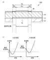
まず、図1を用いて、圧電膜の分散関係k(ω)について説明する。図1の縦軸は角周波数ωであり、縦軸より右側にある横軸は波数kの実数を示し、左側にある横軸は波数kの虚数を示す。波数kが虚数の場合には、圧電膜を伝搬する弾性波は指数関数的に減衰する。また、波数kが0(ゼロ)は遮断周波数を表していて、これは圧電薄膜共振器の共振に主に寄与する厚み縦振動モードの共振周波数である。図1のように、ポアソン比が0.33より大きいタイプIの材料を圧電膜に用いた場合、厚み縦振動モードに加えて付随的に発生する横モードは遮断周波数よりも高い周波数に存在することが分かる。タイプIの材料として、例えば酸化亜鉛(ZnO)がある。一方、ポアソン比が0.33以下のタイプIIの材料を圧電膜に用いた場合、横モードは遮断周波数よりも低い周波数に存在することが分かる。タイプIIの材料として、例えば窒化アルミニウム(AlN)がある。 First, the dispersion relationship k (ω) of the piezoelectric film will be described with reference to FIG. The vertical axis in FIG. 1 is the angular frequency ω, the horizontal axis on the right side of the vertical axis indicates the real number of the wave number k, and the horizontal axis on the left side indicates the imaginary number of the wave number k. When the wave number k is an imaginary number, the elastic wave propagating through the piezoelectric film attenuates exponentially. A wave number k of 0 (zero) represents a cut-off frequency, which is a resonance frequency of the thickness longitudinal vibration mode that mainly contributes to the resonance of the piezoelectric thin film resonator. As shown in FIG. 1, when a type I material having a Poisson's ratio greater than 0.33 is used for the piezoelectric film, a lateral mode that occurs incidentally in addition to the thickness longitudinal vibration mode exists at a frequency higher than the cutoff frequency. I understand that. As a type I material, for example, there is zinc oxide (ZnO). On the other hand, when a type II material having a Poisson's ratio of 0.33 or less is used for the piezoelectric film, it can be seen that the transverse mode exists at a frequency lower than the cutoff frequency. An example of the type II material is aluminum nitride (AlN).
図1では、圧電薄膜共振器の共振に主に寄与する厚み縦振動モードS1の分散曲線の波数kの小さい部分のみを図示している。図2は、圧電膜にAlNを用いた場合の分散特性を波数kの実数の大きい範囲まで示した図である。図2のように、モードS1の分散曲線は、波数k1までは単調に周波数が減少し、波数k1を超えると周波数は単調に増加するようになる。また、モードS1の他にも、モードS0、モードA1、及びモードA0などの多くのモードが存在することが分かる。モードA0は、非対称モードの基底モードである。モードS0は、対称モードの基底モードである。モードA1は、非対称モードの1次モードである。モードS1は、上述したように、圧電薄膜共振器の共振に主に寄与する主モードである。 In FIG. 1, only a portion where the wave number k is small in the dispersion curve of the thickness longitudinal
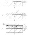
図3(a)は、比較例1に係る圧電薄膜共振器1000の断面図、図3(b)は、共振領域68の中央領域68aと外周領域68bとでの厚み縦振動モードの分散曲線を示す図である。図3(a)のように、比較例1の圧電薄膜共振器1000は、基板60上に下部電極62が形成されている。基板60及び下部電極62上に、AlNからなる圧電膜64が形成されている。圧電膜64を挟み下部電極62と対向する領域(共振領域68)を有するように、圧電膜64上に上部電極66が形成されている。共振領域68は、厚み縦振動モードが共振する領域である。基板60の共振領域68を含む領域に、空隙70が形成されている。 3A is a cross-sectional view of the piezoelectric
共振領域68内の外周領域68bの上部電極66は、共振領域68の中央領域68aの上部電極66に比べ薄くなっている。このため、外周領域68bの遮断周波数は、中央領域68aの遮断周波数よりも高くなっている。 The
図3(b)のように、外周領域68bの遮断周波数が中央領域68aの遮断周波数よりも高いため、外周領域68bでのモードS1の分散曲線は中央領域68aでのモードS1の分散曲線よりも高周波数側に移動する。これにより、中央領域68aの共振周波数よりも低い周波数f0における波数は、外周領域68bでは中央領域68aに比べて実数値が大きくなる。このため、中央領域68aの共振周波数より低い周波数を有して横方向に伝搬する弾性波は、中央領域68aから外部に漏れ易くなる。これにより、共振特性において横モードに起因したスプリアスの発生を抑制できる。しかしながら、中央領域68aから外部に弾性波が漏れることから、共振周波数から反共振周波数の広い範囲にわたってQ値が低下してしまう。 As shown in FIG. 3B, since the cutoff frequency of the outer
図4(a)は、比較例2に係る圧電薄膜共振器1100の断面図、図4(b)は、共振領域68の中央領域68aと第1外周領域68cと第2外周領域68dとでの厚み縦振動モードの分散曲線を示す図である。図4(a)のように、比較例2の圧電薄膜共振器1100では、共振領域68内の外周領域68bは、中央領域68aよりも上部電極66が薄い第1外周領域68cと、中央領域68aよりも上部電極66が厚い第2外周領域68dとで構成されている。このため、第1外周領域68cの遮断周波数は、中央領域68aの遮断周波数よりも高くなっている。第2外周領域68dの遮断周波数は、中央領域68aの遮断周波数よりも低くなっている。4A is a cross-sectional view of the piezoelectric
図4(b)のように、第1外周領域68cの遮断周波数が中央領域68aの遮断周波数よりも高いため、第1外周領域68cでのモードS1の分散曲線は中央領域68aでのモードS1の分散曲線よりも高周波数側に移動する。第2外周領域68dの遮断周波数が中央領域68aの遮断周波数よりも低いため、第2外周領域68dでのモードS1の分散曲線は中央領域68aでのモードS1の分散曲線よりも低周波数側に移動する。これにより、中央領域68aの共振周波数よりも低い周波数f0における波数は、第1外周領域68cでは中央領域68aに比べて実数値が大きくなり、第2外周領域68dでは虚数値となる。このため、中央領域68aの共振周波数より低い周波数を有して横方向に伝搬する弾性波は、中央領域68aから第1外周領域68cに漏れ易くなると共に、第2外周領域68dで漏れが抑制される。横方向に伝搬する弾性波が第1外周領域68cに漏れ易くなることで、共振特性において横モードに起因したスプリアスの発生を抑制でき、且つ、第2外周領域68dで横方向に伝搬する弾性波が反射されることで、共振周波数から反共振周波数の間でのQ値の劣化を抑制できる。しかしながら、遮断周波数が高い第1外周領域68cと遮断周波数が低い第2外周領域68dとを設けているため、中央領域68aの面積が小さくなり、電気機械結合係数k2が低下してしまう。As shown in FIG. 4B, since the cutoff frequency of the first outer
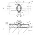
図5(a)は、実施例1に係る圧電薄膜共振器100の断面図、図5(b)は、共振領域20の中央領域20aと外周領域20bとでの厚み縦振動モードの分散曲線を示す図である。図5(a)のように、実施例1の圧電薄膜共振器100は、例えばシリコン(Si)基板からなる基板10上に、下部電極12が形成されている。下部電極12は、例えばクロム(Cr)膜やルテニウム(Ru)膜など金属膜である。基板10及び下部電極12上に、ポアソン比が0.33以下の圧電膜14が形成されている。圧電膜14は、例えばAlNからなる。圧電膜14を挟み下部電極12と対向する領域(共振領域20)を有するように、圧電膜14上に上部電極16が形成されている。上部電極16は、例えばCr膜やRu膜などの金属膜である。共振領域20は、厚み縦振動モードが共振する領域である。基板10の共振領域20を含む領域に、空隙22が形成されている。 5A is a cross-sectional view of the piezoelectric
圧電膜14内には、共振領域20内の外周領域20bに挿入膜18が形成されている。挿入膜18は、共振領域20の中央領域20aには形成されていない。挿入膜18は、例えば二酸化シリコン(SiO2)膜である。なお、共振領域20内の外周領域20bとは、共振領域20内の領域であって、共振領域20の外周を含み、外周に沿った領域である。共振領域20の中央領域20aとは、共振領域20内の領域であって、外周領域20bよりも内側部分であり、共振領域20の中央を含む領域である。In the
外周領域20bの上部電極16は、中央領域20aの上部電極16に比べて薄くなっている。これにより、共振領域20における下部電極12、圧電膜14、挿入膜18、及び上部電極16を含む積層膜の厚さは、外部領域20bで中央領域20aよりも薄くなっている。外周領域20bに挿入膜18が形成され且つ外周領域20bの上部電極16が薄くなっていることで、中央領域20aと外周領域20bとで遮断周波数が同一又はほぼ同一となっている。 The
図5(b)のように、モードS1の分散曲線は、中央領域20aと外周領域20bとで形状が異なっている。外周領域20bでのモードS1の分散曲線は、中央領域20aでのモードS1の分散曲線に比べて、極小周波数付近の曲率が大きくなっている。これは、外周領域20bの圧電膜14内に挿入膜18が形成されているため、下部電極12と上部電極16とで挟まれた材料のポアソン比が、中央領域20aと外周領域20bとで異なるためである。 As shown in FIG. 5B, the shape of the dispersion curve in mode S1 differs between the
中央領域20aでのモードS1の分散曲線と外周領域20bでのモードS1の分散曲線の形状を制御することで、中央領域20aの共振周波数より低い周波数f0における波数の実数値を、外周領域20bで中央領域20aよりも大きくすることができる。言い換えると、モードS1の分散曲線の傾きがゼロとなる周波数を制御することで、中央領域20aの共振周波数より低い周波数f0における波数の実数値を、外周領域20bで中央領域20aよりも大きくすることができる。このため、中央領域20aの共振周波数より低い周波数を有して横方向に伝搬する弾性波は、中央領域20aから外部に漏れ易くなり、共振特性において横モードに起因したスプリアスの発生を抑制できる。また、挿入膜18を設けることで、共振周波数から反共振周波数の間でのモードS0の弾性波の発生を弱めることができる。モードS0の弾性波の発生自体が弱まることから、弾性波の漏れも弱められ、その結果、共振周波数から反共振周波数の間でのQ値の劣化を抑制することができる。また、中央領域20aの遮断周波数と外周領域20bの遮断周波数を同一又は同等に近づけることができるため、電気機械結合係数k2の劣化を抑制することができる。 By controlling the shape of the dispersion curve of the mode S1 in the
以上のように、実施例1によれば、図5(a)のように、共振領域20内の外周領域20bに挿入膜18が設けられ、且つ、外周領域20bの上部電極16が中央領域20aに比べて薄くなっている。これによって、図5(a)及び図5(b)のように、外周領域20bと中央領域20aの遮断周波数がほぼ同じで、外周領域20bにおける遮断周波数と厚み縦振動モードの分散曲線の極小周波数との差が、中央領域20aにおける遮断周波数と厚み縦振動モードの分散曲線の極小周波数との差よりも小さくなっている。これにより、上述したように、Q値及び電気機械結合係数k2の劣化を抑制しつつ、スプリアスを抑制することができる。なお、遮断周波数がほぼ同じとは、完全に同じ場合の他に、電気機械結合係数k2の劣化を抑制できる程度に同じ場合を含む。 As described above, according to the first embodiment, as shown in FIG. 5A, the
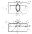
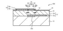
図6(a)は、実施例2に係る圧電薄膜共振器200の上面図、図6(b)及び図6(c)は、図6(a)のA−A間の断面図である。図6(b)は、ラダー型フィルタの直列共振子Sの断面図、図6(c)は、ラダー型フィルタの並列共振子Pの断面図である。 FIG. 6A is a top view of the piezoelectric
図6(a)及び図6(b)のように、直列共振子Sは、基板10上に、下部電極12が形成されている。基板10の平坦主面と下部電極12との間に、下部電極12側にドーム状の膨らみを有する空隙22が形成されている。ドーム状の膨らみとは、例えば空隙22の周辺では空隙22の高さが低く、空隙22の内部ほど空隙22の高さが高くなるような形状の膨らみである。下部電極12は、下層12aと上層12bとを含む。下層12aは、例えばCr膜であり、上層12bは、例えばRu膜である。 As shown in FIGS. 6A and 6B, the series resonator S has the
基板10及び下部電極12上に、(002)方向を主軸とするAlNを主成分とする圧電膜14が形成されている。圧電膜14を挟み下部電極12と対向する領域(共振領域20)を有するように、圧電膜14上に上部電極16が形成されている。上部電極16は、下層16aと上層16bとを含む。下層16aは、例えばRu膜であり、上層16bは、例えばCr膜である。共振領域20は、例えば楕円形形状を有し、厚み縦振動モードが共振する領域である。 On the
圧電膜14内には、共振領域20内の外周領域20bに挿入膜18が形成されている。挿入膜18は、共振領域20の中央領域20aには形成されていない。挿入膜18は、例えばSiO2膜である。挿入膜18は、共振領域20内の外周領域20bの全周にわたって形成されていて、外周領域20bから共振領域20の外側にまで延在して形成されている。挿入膜18は、圧電膜14の膜厚方向の中央部分に形成されていてもよいし、中央部分以外に形成されていてもよい。なお、実施例1に記載したように、外周領域20bとは、共振領域20内の領域であって、共振領域20の外周を含み外周に沿った領域である。外周領域20bは、例えばリング状をしている。共振領域20の中央領域20aとは、共振領域20内の領域であって、外周領域20bよりも内側部分であり、共振領域20の中央を含む領域である。In the
外周領域20bの上部電極16は、外周領域20bの全周にわたって、中央領域20aの上部電極16に比べて薄くなっている。例えば、上部電極16の下層16aの厚さが、中央領域20aよりも外周領域20bで薄くなっていて、上部電極16の上層16bの厚さは、中央領域20aと外周領域20bとで同じになっている。上部電極16上に、周波数調整膜24として酸化シリコン膜が形成されている。なお、周波数調整膜24は、パッシベーション膜として機能してもよい。上部電極16が中央領域20aよりも外周領域20bで薄いことで、共振領域20における下部電極12、圧電膜14、挿入膜18、上部電極16、及び周波数調整膜24を含む積層膜の厚さは、外部領域20bで中央領域20aよりも薄くなっている。 The
下部電極12及び圧電膜14には、犠牲層をエッチングするための導入路28が形成されている。犠牲層は、空隙22を形成するための層である。導入路28の先端付近は、下部電極12及び圧電膜14で覆われておらず、孔部30が形成されている。 In the
図6(a)及び図6(c)のように、並列共振子Pは、直列共振子Sと比較し、上部電極16の下層16aと上層16bとの間であって、共振領域20に、質量負荷膜26が形成されている。質量負荷膜26は、例えばチタン(Ti)膜である。その他の構成は、直列共振子Sと同じであるため説明を省略する。 6A and 6C, the parallel resonator P is between the
直列共振子Sと並列共振子Pとの間の共振周波数の差は、質量負荷膜26の膜厚によって調整できる。直列共振子Sと並列共振子Pの両方の共振周波数の調整は、周波数調整膜24の膜厚によって行うことができる。 The difference in resonance frequency between the series resonator S and the parallel resonator P can be adjusted by the film thickness of the
例えば2GHzの共振周波数を有する圧電薄膜共振器の場合、下部電極12のCr膜からなる下層12aの厚さは100nm、Ru膜からなる上層12bの厚さは250nmである。AlN膜からなる圧電膜14の厚さは1100nmであり、圧電膜14内の挿入膜18の厚さは150nmである。上部電極16のRu膜からなる下層16aの厚さは、共振領域20の中央領域20aで230nm、外周領域20bで50nmである。上部電極16のCr膜からなる上層16bの厚さは50nmである。酸化シリコン膜からなる周波数調整膜24の厚さは50nmである。Ti膜からなる質量負荷膜26の厚さは120nmである。なお、各層の厚さは、所望の共振特性を得るために適宜設計することができる。 For example, in the case of a piezoelectric thin film resonator having a resonance frequency of 2 GHz, the thickness of the
基板10としては、Si基板以外に、例えば石英基板、ガラス基板、セラミック基板、又はガリウム砒素(GaAs)基板などを用いることができる。下部電極12及び上部電極16としては、Cr及びRu以外にも、例えばアルミニウム(Al)、チタン(Ti)、銅(Cu)、モリブデン(Mo)、タングステン(W)、タンタル(Ta)、白金(Pt)、ロジウム(Rh)、又はイリジウム(Ir)などの金属単層膜又はこれらの積層膜を用いることができる。圧電膜14は、ポアソン比が0.33以下の材料であれば、AlN以外の材料を用いることができる。また、圧電膜14は、AlNを主成分とし、共振特性の向上又は圧電性の向上のために、他の元素を含んでもよい。例えば、添加元素としてスカンジウム(Sc)を用いることにより、圧電膜14の圧電性を向上できる。 As the
周波数調整膜24としては、酸化シリコン膜以外にも、窒化シリコン膜又は窒化アルミニウム膜などを用いることができる。質量負荷膜26としては、Ti以外にも、Ru、Cr、Al、Cu、Mo、W、Ta、Pt、Rh、又はIrなどの金属単層膜又はこれらの積層膜を用いることができる。また、例えば窒化シリコン又は酸化シリコンなどの窒化金属又は酸化金属からなる絶縁膜を用いることもできる。質量負荷膜26は、上部電極16の層間以外にも、例えば下部電極12の下、下部電極12の層間、上部電極16の上、下部電極12と圧電膜14の間、又は圧電膜14と上部電極16の間に形成することができる。質量負荷膜26は、共振領域20を含むように形成されていれば、共振領域20より大きくてもよい。 As the
次に、実施例2の圧電薄膜共振器200の製造方法を、直列共振子Sの場合を例に説明する。図7(a)から図7(c)は、実施例2に係る圧電薄膜共振器200の製造方法を示す断面図である。図7(a)のように、基板10の平坦主面上に空隙22を形成するために犠牲層32を成膜する。犠牲層32は、例えばスパッタリング法、真空蒸着法、又はCVD(Chemical Vapor Deposition)法を用い成膜される。犠牲層32は、例えば酸化マグネシウム(MgO)、酸化亜鉛(ZnO)、ゲルマニウム(Ge)、又は二酸化シリコン(SiO2)などのエッチング液又はエッチングガスに容易に溶解する材料を用いることができる。犠牲層32の厚さは、例えば10nm〜100nm程度である。その後、犠牲層32を、フォトリソグラフィ技術及びエッチング技術を用いて、所望の形状にパターニングする。犠牲層32の形状は、空隙22の平面形状に相当する形状であり、例えば共振領域20となる領域を含む。Next, a method for manufacturing the piezoelectric
次に、犠牲層32及び基板10上に、下部電極12として下層12a及び上層12bを成膜する。下部電極12は、例えばスパッタリング法、真空蒸着法、又はCVD法を用い成膜される。その後、下部電極12を、フォトリソグラフィ技術及びエッチング技術を用いて、所望の形状にパターニングする。なお、下部電極12をリフトオフ法によって形成してもよい。 Next, the
図7(b)のように、下部電極12及び基板10上に、第1圧電膜14aと挿入膜18を成膜する。第1圧電膜14aと挿入膜18は、例えばスパッタリング法、真空蒸着法、又はCVD法を用い成膜される。その後、挿入膜18を、フォトリソグラフィ技術及びエッチング技術を用いて、所望の形状にパターニングする。なお、挿入膜18をリフトオフ法によって形成してもよい。 As shown in FIG. 7B, the first
図7(c)のように、第1圧電膜14a及び挿入膜18上に、第2圧電膜14bを成膜する。第2圧電膜14bは、例えばスパッタリング法、真空蒸着法、又はCVD法を用い成膜される。第1圧電膜14a及び第2圧電膜14bから圧電膜14が形成される。圧電膜14上に、上部電極16として下層16a及び上層16bを成膜する。上部電極16は、例えばスパッタリング法、真空蒸着法、又はCVD法を用い成膜される。ここで、上部電極16の下層16aは、共振領域20の中央領域20aと外周領域20bとで膜厚を異ならせるように形成する。形成方法は、相対的に膜厚が薄い外周領域20bにおける厚さで下層16aを全面に成膜した後、中央領域20aに下層16aを追加で成膜してもよい。若しくは、相対的に膜厚が厚い中央領域20aにおける厚さで下層16aを全面に成膜した後、外周領域20bに成膜された下層16aに対してエッチングを行うことで形成してもよい。その後、上部電極16を、フォトリソグラフィ技術及びエッチング技術を用いて、所望の形状にパターニングする。上部電極16上に、例えばスパッタリング法又はCVD法を用いて周波数調整膜24を成膜する。 As illustrated in FIG. 7C, the second
なお、図6(c)の並列共振子Pにおいては、上部電極16の下層16aを形成した後、質量負荷膜26を、例えばスパッタリング法、真空蒸着法、又はCVD法を用い成膜する。質量負荷膜26をフォトリソグラフィ技術及びエッチング技術を用いて、所望の形状にパターニングする。その後に、上部電極16の上層16bを形成する。 In the parallel resonator P of FIG. 6C, after forming the
周波数調整膜24を形成した後、孔部30及び導入路28(図6(a)参照)を介し、犠牲層32のエッチング液を、下部電極12下の犠牲層32に導入する。これにより、犠牲層32が除去される。犠牲層32をエッチングする媒体としては、犠牲層32以外の共振器を構成する材料をエッチングしない媒体であることが好ましい。例えば、エッチング媒体は、エッチング媒体が接触する下部電極12及び圧電膜14がエッチングされない媒体であることが好ましい。下部電極12、圧電膜14、及び上部電極16を含む積層膜の応力を圧縮応力となるように設定しておくことにより、犠牲層32が除去されると、積層膜が基板10の反対側に基板10から離れるように膨れる。これにより、基板10と下部電極12の間にドーム状の膨らみを有する空隙22が形成される。以上の工程を含んで、実施例2の圧電薄膜共振器200が形成される。 After the
次に、実施例2の圧電薄膜共振器200に対して発明者が行ったシミュレーションについて説明する。発明者は、図6(a)及び図6(b)に示す実施例2の圧電薄膜共振器200に対し、外周領域20bの上部電極16の膜厚が共振周波数よりも低周波数側に発生するスプリアスに及ぼす影響について有限要素法を用いて調査した。シミュレーションは、第1、第2試験体(実施例2)及び第3試験体(比較例3)に対して行った。 Next, a simulation performed by the inventor on the piezoelectric
第1試験体は、下部電極12の下層12aを厚さ100nmのCr膜、上層12bを厚さ200nmのRu膜とし、圧電膜14を厚さ1260nmのAlN膜とした。上部電極16はRu膜からなる下層16aのみで構成され、中央領域20aにおける厚さを230nmとし、外周領域20bにおける厚さを50nmとした。挿入膜18は、厚さ125nmのSiO2膜とし、共振領域20に挿入されている長さ(すなわち、外周領域20bの幅)を2.5μmとした。In the first test body, the
第2試験体は、外周領域20bにおける上部電極16の厚さを60nmとし、その他は、第1試験体と同じにした。第3試験体は、外周領域20bにおける上部電極16の厚さを、中央領域20aにおける厚さと同じ230nmとし、その他は、第1試験体と同じにした。 In the second test body, the thickness of the
表1に、第1〜第3試験体の共振領域20の中央領域20aと外周領域20bとの遮断周波数のシミュレーション結果を示す。表1のように、第1試験体では、中央領域20aと外周領域20bの遮断周波数が同じ値となり、第2試験体では、中央領域20aと外周領域20bの遮断周波数が近い値になった。第3試験体では、中央領域20aと外周領域20bの遮断周波数は離れた値となった。
図8(a)及び図8(b)は、スプリアスを調査したシミュレーションの結果を示す図である。図8(a)は、共振周波数付近の反射特性(S11)であり、図8(b)は、スミスチャートである。第1試験体のシミュレーション結果を実線で示し、第2試験体のシミュレーション結果を一点鎖線で示し、第3試験体のシミュレーション結果を点線で示している。表1及び図8(a)、図8(b)のように、上部電極16の厚さを中央領域20aよりも外周領域20bで薄くして中央領域20aと外周領域20bの遮断周波数を近づけることにより、共振周波数よりも低周波数側に発生するスプリアスを低減できることが確認できた。 FIG. 8A and FIG. 8B are diagrams showing the results of a simulation for examining spurious. FIG. 8A is a reflection characteristic (S11) near the resonance frequency, and FIG. 8B is a Smith chart. The simulation result of the first specimen is indicated by a solid line, the simulation result of the second specimen is indicated by a one-dot chain line, and the simulation result of the third specimen is indicated by a dotted line. As shown in Table 1 and FIGS. 8A and 8B, the thickness of the
次に、発明者は、第1試験体に対して、中央領域20aと外周領域20bとでの厚み縦振動モードの分散曲線について有限要素法を用いて調査した。図9(a)及び図9(b)は、分散曲線を調査したシミュレーションの結果を示す図である。図9(a)は、中央領域20aでの厚み縦振動モードの分散曲線を示し、図9(b)は、外周領域20bでの厚み縦振動モードの分散曲線を示している。図9(a)及び図9(b)のように、波数が0(ゼロ)である遮断周波数は共に2010MHzであり、モードS1の分散曲線の極小周波数(傾きがゼロとなる周波数)はそれぞれ約1905MHz、約1935MHzであった。このことから、外周領域20bにおける遮断周波数と厚み縦振動モードの分散曲線の極小周波数との差を、中央領域20aにおける遮断周波数と厚み縦振動モードの分散曲線の極小周波数との差よりも小さくすることで、共振周波数よりも低周波数側に発生するスプリアスを低減できることが確認できた。 Next, the inventor investigated the dispersion curve of the thickness longitudinal vibration mode in the
したがって、外周領域20bに挿入膜18を形成し且つ外周領域20bの上部電極16の膜厚を中央領域20aよりも薄くして、外周領域20bと中央領域20aの遮断周波数をほぼ同じにし、外周領域20bにおける遮断周波数と厚み縦振動モードの分散曲線の極小周波数との差を、中央領域20aにおける遮断周波数と厚み縦振動モードの分散曲線の極小周波数との差よりも小さくする。これにより、スプリアスを抑制できることがシミュレーションからも確認できた。 Therefore, the
次に、発明者は、第1試験体に対して、反共振周波数のQ値及び電気機械結合係数k2について有限要素法を用いて調査した。また、比較のために、図4(a)に示した比較例2の圧電薄膜共振器1100である第4試験体に対してもシミュレーションを行った、第4試験体は、上部電極66の厚さは、中央領域68aで230nm、第1外周領域68cで220nm、第2外周領域68dで330nmとした。また、第1外周領域68cの長さを4.0μm、第2外周領域68dの長さを2.5μmとした。その他は、第1試験体と同じにした。表2に、反共振周波数のQ値及び電気機械結合係数k2のシミュレーション結果を示す。表2のように、第1試験体は、第4試験体に比べて、反共振周波数のQ値及び電気機械結合係数k2が改善された結果となった。
したがって、外周領域20bに挿入膜18を形成し且つ外周領域20bの上部電極16の膜厚を中央領域20aよりも薄くして、外周領域20bと中央領域20aの遮断周波数をほぼ同じにし、外周領域20bにおける遮断周波数と厚み縦振動モードの分散曲線の極小周波数との差を、中央領域20aにおける遮断周波数と厚み縦振動モードの分散曲線の極小周波数との差よりも小さくする。これにより反共振周波数のQ値及び電気機械結合係数k2を改善できることがシミュレーションからも確認できた。 Therefore, the
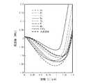
次に、発明者は、挿入膜18に様々な材料を用いた圧電薄膜共振器の外周領域20bでの厚み縦振動モードの分散曲線について有限要素法を用いて調査した。シミュレーションに用いた圧電薄膜共振器は、挿入膜18以外は第1試験体と同じにした。挿入膜18は、厚さ125nm、長さ1.9μmとした。表3は、シミュレーションに用いた挿入膜18の種類とそれぞれの材料定数とを示している。なお、表3では、音響インピーダンスは、密度とヤング率の積に対してAlNの音響インピーダンスで規格化した値を示している。表3のように、挿入膜18に、SiO2、Ru、Cr、Ti、Al、Ta、W、又はMoを用いてシミュレーションを行った。
図10は、挿入膜18に様々な材料を用いた圧電薄膜共振器の共振領域20内の外周領域20bでの厚み縦振動モードの分散曲線を調査したシミュレーションの結果を示す図である。なお、共振領域20の中央領域20aでの厚み縦振動モードの分散曲線を太破線で示している。図10のように、挿入膜18がSiO2又はAlである場合に、外周領域20bでの厚み縦振動モードの分散曲線の極小周波数が、中央領域20aでの厚み縦振動モードの分散曲線の極小周波数よりも高周波数側に移動していることが分かる。FIG. 10 is a diagram showing the results of a simulation in which the dispersion curve of the thickness longitudinal vibration mode in the outer
次に、発明者は、挿入膜18に様々な材料を用いた圧電薄膜共振器の共振周波数付近の反射特性(S11)について有限要素法を用いて調査した。また、比較のために、挿入膜18が設けられていない圧電薄膜共振器の共振周波数付近の反射特性(S11)についても調査した。図11(a)及び図11(b)は、シミュレーションに用いた圧電薄膜共振器を示す断面図である。図11(a)のように、Siからなる基板10上の下部電極12の下層12aを厚さ100nmのCr膜とし、上層12bを厚さ200nmのRu膜とした。圧電膜14を厚さ1260nmのAlN膜とした。上部電極16はRu膜のみで構成され、中央領域20aにおける厚さは230nmとし、外周領域20bにおける厚さは、外周領域20bの遮断周波数が中央領域20aの遮断周波数と一致するようにした。挿入膜18は、厚さ125nm、長さ1.9μmとした。図11(b)のように、挿入膜18が設けられていない圧電薄膜共振器は、上部電極16はRu膜のみで構成され、厚さを230nmと一定にした。その他は、図11(a)と同じである。 Next, the inventor investigated the reflection characteristic (S11) near the resonance frequency of the piezoelectric thin film resonator using various materials for the
図12(a)は、挿入膜18が設けられていない圧電薄膜共振器の共振周波数付近の反射特性(S11)のシミュレーションの結果を示す図である。図12(b)から図13(c)は、挿入膜18に様々な材料を用いた圧電薄膜共振器の共振周波数付近の反射特性(S11)のシミュレーションの結果を示す図である。図12(a)から図13(c)のように、挿入膜18がSiO2膜、Ti膜、又はAl膜である場合に、共振周波数以下のスプリアスを抑制できることが分かった。特に、挿入膜18がSiO2膜である場合に、共振周波数以下のスプリアスを大きく抑制できることが分かった。FIG. 12A is a diagram showing a result of simulation of the reflection characteristic (S11) near the resonance frequency of the piezoelectric thin film resonator in which the
したがって、挿入膜18は、スプリアスを抑制する点から、Ti、Alのような、AlNよりも音響インピーダンスの小さい膜であることが好ましく、SiO2のような、AlNよりも音響インピーダンスが小さく且つポアソン比が小さい膜であることがより好ましい。また、挿入膜18は、他の元素を含む酸化シリコン膜であってもよい。他の元素として、例えばフッ素又はボロンなどが挙げられる。このような元素を含む酸化シリコン膜の場合でも、AlNよりも音響インピーダンスが小さく且つポアソン比が小さくなる。Therefore, the
実施例2によれば、図6(a)から図6(c)のように、挿入膜18は、外周領域20bの全周にわたって形成され、且つ、外周領域20bの全周における上部電極16は、中央領域20aの上部電極16に比べて薄くなっている。これにより、スプリアスを効果的に抑制することができる。 According to the second embodiment, as shown in FIGS. 6A to 6C, the
図14(a)は、実施例2の変形例1に係る圧電薄膜共振器210の上面図、図14(b)は、図14(a)のA−A間の断面図である。なお、図14(b)はラダー型フィルタの直列共振子Sの断面図であり、並列共振子Pについては、図6(c)と同様、図14(a)の上部電極16の層間に質量負荷膜26が設けられた構造であるため図示を省略する(実施例2の変形例2から実施例5においても同じ)。 14A is a top view of the piezoelectric
図14(a)及び図14(b)のように、実施例2の変形例1の圧電薄膜共振器210では、上部電極16は、共振領域20内の外周領域20bだけでなく、外周領域20bから共振領域20の外側にかけて薄くなっている。その他の構成は、実施例2の圧電薄膜共振器200と同じであるため説明を省略する。 As shown in FIGS. 14A and 14B, in the piezoelectric
図15(a)は、実施例2の変形例2に係る圧電薄膜共振器220の上面図、図15(b)は、図15(a)のA−A間の断面図である。図15(a)及び図15(b)のように、実施例2の変形例2の圧電薄膜共振器220では、挿入膜18は、圧電膜14の上面に形成されている。言い換えると、挿入膜18は、圧電膜14と上部電極16の間に形成されている。その他の構成は、実施例2の圧電薄膜共振器200と同じであるため説明を省略する。 15A is a top view of the piezoelectric
図16(a)は、実施例2の変形例3に係る圧電薄膜共振器230の上面図、図16(b)は、図16(a)のA−A間の断面図である。図16(a)及び図16(b)のように、実施例2の変形例3の圧電薄膜共振器230では、挿入膜18は、圧電膜14の下面に形成されている。言い換えると、挿入膜18は、圧電膜14と下部電極12の間に形成されている。その他の構成は、実施例2の圧電薄膜共振器200と同じであるため説明を省略する。 16A is a top view of the piezoelectric
実施例2、実施例2の変形例2、及び実施例2の変形例3のように、挿入膜18は、圧電膜14内に形成されてもよいし、圧電膜14の上面又は下面に形成されてもよい。また、挿入膜18が、圧電膜14内、圧電膜14の上面、及び圧電膜14の下面の複数に形成されてもよい。 As in the second embodiment, the second modification of the second embodiment, and the third modification of the second embodiment, the
図17(a)は、実施例2の変形例4に係る圧電薄膜共振器240の上面図、図17(b)は、図17(a)のA−A間の断面図である。図17(a)及び図17(b)のように、実施例2の変形例4の圧電薄膜共振器240では、挿入膜18は、共振領域20内の外周領域20bの一部にのみ設けられている。その他の構成は、実施例2の圧電薄膜共振器200と同じであるため説明を省略する。 FIG. 17A is a top view of the piezoelectric
図18(a)は、実施例2の変形例5に係る圧電薄膜共振器250の上面図、図18(b)は、図18(a)のA−A間の断面図である。図18(a)及び図18(b)のように、実施例2の変形例5の圧電薄膜共振器250では、上部電極16は、共振領域20内の外周領域20bの一部でのみ薄くなっている。その他の構成は、実施例2の圧電薄膜共振器200と同じであるため説明を省略する。 FIG. 18A is a top view of the piezoelectric
なお、実施例2から実施例2の変形例5では、外周領域20bの上部電極16の下層16aが中央領域20aよりも薄い場合を例に示したが、外周領域20bの上部電極16の上層16bが薄い場合でもよいし、下層16aと上層16bの両方が薄い場合でもよい。また、上部電極16は、下層16aと上層16bの2層構造の場合に限られず、単層構造の場合や、3層以上の層構造の場合でもよい。下部電極12も同様に、単層構造や3層以上の層構造の場合でもよい。 In the modification 5 of the second embodiment to the second embodiment, the case where the
図19(a)は、実施例3に係る圧電薄膜共振器300の上面図、図19(b)は、図19(a)のA−A間の断面図である。図19(a)及び図19(b)のように、実施例3の圧電薄膜共振器300では、共振領域20内の外周領域20bでは、上部電極16の下層16aが形成されてなく、上層16bだけが形成されている。その他の構成は、実施例2の圧電薄膜共振器200と同じであるため説明を省略する。 FIG. 19A is a top view of the piezoelectric
実施例3のように、共振領域20内の外周領域20bの上部電極16が、中央領域20aの上部電極16に比べて金属層の層数が少ないことで、外周領域20bの上部電極16が中央領域20aの上部電極16よりも薄くなっていてもよい。 As in Example 3, the
図20(a)は、実施例4に係る圧電薄膜共振器400の上面図、図20(b)は、図20(a)のA−A間の断面図である。図20(a)及び図20(b)のように、実施例4の圧電薄膜共振器400では、共振領域20内の外周領域20bの圧電膜14が、中央領域20aの圧電膜14よりも薄くなっている。上部電極16は、中央領域20a及び外周領域20bで同じ厚さになっている。その他の構成は、実施例2の圧電薄膜共振器200と同じであるため説明を省略する。 20A is a top view of the piezoelectric
図21(a)は、実施例5に係る圧電薄膜共振器500の上面図、図21(b)は、図21(a)のA−A間の断面図である。図21(a)及び図21(b)のように、実施例5の圧電薄膜共振器500では、共振領域20内の外周領域20bの下部電極12が、中央領域20aの下部電極12よりも薄くなっている。上部電極16は、中央領域20a及び外周領域20bで同じ厚さになっている。その他の構成は、実施例2の圧電薄膜共振器200と同じであるため説明を省略する。 FIG. 21A is a top view of the piezoelectric
実施例2から実施例5のように、共振領域20内の外周領域20bの下部電極12、圧電膜14、及び上部電極16の少なくとも1つが、中央領域20aに比べて薄くなっていればよい。外周領域20bの下部電極12、圧電膜14、及び上部電極16のうちの2以上が、中央領域20aに比べて薄くなっていてもよい。 As in the second to fifth embodiments, at least one of the
なお、実施例5においても、実施例2の変形例1と同様に、下部電極12は、共振領域20内の外周領域20bだけでなく、外周領域20bから共振領域20の外側にかけて薄くなっていてもよい。実施例2の変形例5と同様に、下部電極12は、外周領域20bの一部でのみ薄くなっていてもよい。 In the fifth embodiment, as in the first modification of the second embodiment, the
なお、実施例5においても、実施例3と同様に、共振領域20内の外周領域20bの下部電極12が、中央領域20aの下部電極12に比べて金属層の層数が少ないことで、外周領域20bの下部電極12が中央領域20aの下部電極12よりも薄くなっていてもよい。すなわち、外周領域20bの上部電極16及び下部電極12の少なくとも一方が、中央領域20aの上部電極16及び下部電極12の前記少なくとも一方に比べて、金属層の層数が少なくなっていてもよい。 In Example 5, as in Example 3, the
なお、実施例5では、外周領域20bの下部電極12の下層12aが中央領域20aよりも薄い場合を例に示したが、外周領域20bの下部電極12の上層12bが薄い場合でもよいし、下層12aと上層12bの両方が薄い場合でもよい。 In the fifth embodiment, the case where the
なお、実施例3から実施例5においても、実施例2の変形例2、変形例3と同様に、挿入膜18は、圧電膜14の上面又は下面に形成されていてもよい。 In the third to fifth embodiments, the
図22は、実施例6に係る圧電薄膜共振器600の断面図である。図22のように、実施例6の圧電薄膜共振器600は、基板10の主面に窪みが形成されている。下部電極12は、基板10の主面上に、ほぼ平坦に形成されている。これにより、基板10の窪みが空隙22aとして機能する。空隙22aは、共振領域20を含むように形成されている。その他の構成は、実施例2の圧電薄膜共振器200と同じであるため説明を省略する。なお、空隙22aは、基板10を貫通するように形成されていてもよい。 FIG. 22 is a cross-sectional view of the piezoelectric
実施例6では、実施例2の空隙22の代わりに空隙22aが形成されている場合を例に示したが、実施例2の変形例1から実施例5においても、空隙22の代わりに空隙22aが形成されている場合でもよい。 In the sixth embodiment, the case where the
図23は、実施例7に係る圧電薄膜共振器700の断面図である。図23のように、実施例7の圧電薄膜共振器700は、共振領域20の下部電極12下に音響反射膜40が形成されている。音響反射膜40は、圧電膜14を伝搬する弾性波を反射する膜であり、音響インピーダンスの低い膜42と高い膜44とが交互に形成されている。音響インピーダンスの低い膜42と高い膜44の膜厚は、λ/4(λは弾性波の波長)が基本であるが、所望の特性を得るために適宜変更することができる。また、音響インピーダンスの低い膜42と高い膜44の積層数は任意に設定できる。その他の構成は、実施例2の圧電薄膜共振器200と同じであるため説明を省略する。 FIG. 23 is a cross-sectional view of the piezoelectric
実施例7では、実施例2の空隙22の代わりに音響反射膜40が形成されている場合を例に示したが、実施例2の変形例1から実施例5においても、空隙22の代わりに音響反射膜40を形成してもよい。 In the seventh embodiment, the case where the
このように、圧電薄膜共振器は、実施例1から実施例6のように、共振領域20における下部電極12と基板10との間に空隙22、22aが設けられたFBAR(Film Bulk Acoustic Resonator)の場合でもよい。実施例7のように、共振領域20における下部電極12の下に音響反射膜40が設けられたSMR(Solidly Mounted Resonator)の場合でもよい。 As described above, the piezoelectric thin film resonator is an FBAR (Film Bulk Acoustic Resonator) in which the
実施例2から実施例7では、共振領域20が楕円形形状を有している場合を例に説明したが、四角形又は五角形等の多角形形状を有している場合等、その他の形状を有している場合でもよい。 In
図24は、実施例8に係るフィルタ800を示す図である。図24のように、実施例8のフィルタ800は、入出力端子T1、T2の間に直列に接続された1又は複数の直列共振器S1〜S4と、並列に接続された1又は複数の並列共振器P1〜P4と、を備えたラダー型フィルタである。直列共振器S1〜S4及び並列共振器P1〜P4の少なくとも1つを、実施例1から実施例7の圧電薄膜共振器とすることができる。 FIG. 24 is a diagram illustrating the
図25は、実施例9に係る分波器900を示す図である。図25のように、実施例9の分波器900は、アンテナ端子Antと送信端子Txの間に接続された送信フィルタ50と、アンテナ端子Antと受信端子Rxの間に接続された受信フィルタ52と、を含む。送信フィルタ50と受信フィルタ52は、通過帯域が異なっている。送信フィルタ50は、送信端子Txから入力された信号のうち送信帯域の信号を送信信号としてアンテナ端子Antに通過させ、他の帯域の信号を抑圧する。受信フィルタ52は、アンテナ端子Antから入力された信号のうち受信帯域の信号を受信信号として受信端子Rxに通過させ、他の帯域の信号を抑圧する。送信フィルタ50及び受信フィルタ52の少なくとも一方を、実施例8のフィルタとすることができる。 FIG. 25 is a diagram illustrating a
以上、本発明の実施例について詳述したが、本発明はかかる特定の実施例に限定されるものではなく、特許請求の範囲に記載された本発明の要旨の範囲内において、種々の変形・変更が可能である。 Although the embodiments of the present invention have been described in detail above, the present invention is not limited to such specific embodiments, and various modifications and changes can be made within the scope of the gist of the present invention described in the claims. It can be changed.
10 基板
12 下部電極
14 圧電膜
16 上部電極
18 挿入膜
20 共振領域
20a 中央領域
20b 外周領域
22 空隙
24 周波数調整膜
26 質量負荷膜
28 導入路
30 孔部
32 犠牲層
40 音響反射膜
42 音響インピーダンスの低い膜
44 音響インピーダンスの高い膜
50 送信フィルタ
52 受信フィルタ
DESCRIPTION OF
Claims (14)
Translated fromJapanese前記基板上に設けられ、ポアソン比が0.33以下の圧電膜と、
前記圧電膜を挟んで対向した下部電極及び上部電極と、
前記圧電膜を挟み前記下部電極と前記上部電極とが対向する共振領域内の外周領域の前記圧電膜内若しくは前記圧電膜の下面又は上面に設けられ、前記共振領域の中央領域には設けられていない挿入膜と、を備え、
前記共振領域内の外周領域の前記下部電極、前記圧電膜、及び前記上部電極の少なくとも1つは、対応する前記共振領域の中央領域の前記下部電極、前記圧電膜、及び前記上部電極の前記少なくとも1つに比べて薄く、
前記共振領域内の外周領域の遮断周波数と前記共振領域の中央領域の遮断周波数とは、ほぼ同じであることを特徴とする圧電薄膜共振器。A substrate,
A piezoelectric film provided on the substrate and having a Poisson's ratio of 0.33 or less;
A lower electrode and an upper electrode facing each other across the piezoelectric film;
Provided in the piezoelectric film or on the lower surface or the upper surface of the piezoelectric film in the outer peripheral region in the resonance region where the lower electrode and the upper electrode face each other across the piezoelectric film, and in the central region of the resonance region No insertion membrane, and
At least one of the lower electrode, the piezoelectric film, and the upper electrode in the outer peripheral area in the resonance area is the at least one of the lower electrode, the piezoelectric film, and the upper electrode in the corresponding central area of the resonance area. Thin compared to one,
The piezoelectric thin film resonator according to claim 1, wherein a cutoff frequency of an outer peripheral region in the resonance region is substantially the same as a cutoff frequency of a central region of the resonance region.
前記基板上に設けられ、ポアソン比が0.33以下の圧電膜と、
前記圧電膜を挟んで対向した下部電極及び上部電極と、
前記圧電膜を挟み前記下部電極と前記上部電極とが対向する共振領域内の外周領域の前記圧電膜内若しくは前記圧電膜の下面又は上面に設けられ、前記共振領域の中央領域には設けられていない挿入膜と、を備え、
前記共振領域内の外周領域の前記下部電極、前記圧電膜、及び前記上部電極の少なくとも1つは、対応する前記共振領域の中央領域の前記下部電極、前記圧電膜、及び前記上部電極の前記少なくとも1つに比べて薄く、
前記共振領域内の外周領域における遮断周波数と厚み縦振動モードの分散曲線の極小周波数との差は、前記共振領域の中央領域における遮断周波数と厚み縦振動モードの分散曲線の極小周波数との差よりも小さいことを特徴とする圧電薄膜共振器。A substrate,
A piezoelectric film provided on the substrate and having a Poisson's ratio of 0.33 or less;
A lower electrode and an upper electrode facing each other across the piezoelectric film;
Provided in the piezoelectric film or on the lower surface or the upper surface of the piezoelectric film in the outer peripheral region in the resonance region where the lower electrode and the upper electrode face each other across the piezoelectric film, and in the central region of the resonance region No insertion membrane, and
At least one of the lower electrode, the piezoelectric film, and the upper electrode in the outer peripheral area in the resonance area is the at least one of the lower electrode, the piezoelectric film, and the upper electrode in the corresponding central area of the resonance area. Thin compared to one,
The difference between the cutoff frequency in the outer peripheral region in the resonance region and the minimum frequency of the dispersion curve of the thickness longitudinal vibration mode is based on the difference between the cutoff frequency in the center region of the resonance region and the minimum frequency of the dispersion curve of the thickness longitudinal vibration mode. A piezoelectric thin film resonator characterized by being small.
前記基板上に設けられ、ポアソン比が0.33以下の圧電膜と、
前記圧電膜を挟んで対向した下部電極及び上部電極と、
前記圧電膜を挟み前記下部電極と前記上部電極とが対向する共振領域内の外周領域の前記圧電膜内若しくは前記圧電膜の下面又は上面に設けられ、前記共振領域の中央領域には設けられていない挿入膜と、を備え、
前記共振領域内の外周領域の遮断周波数と前記共振領域の中央領域の遮断周波数とは、ほぼ同じであり、
前記共振領域内の外周領域における遮断周波数と厚み縦振動モードの分散曲線の極小周波数との差は、前記共振領域の中央領域における遮断周波数と厚み縦振動モードの分散曲線の極小周波数との差よりも小さいことを特徴とする圧電薄膜共振器。A substrate,
A piezoelectric film provided on the substrate and having a Poisson's ratio of 0.33 or less;
A lower electrode and an upper electrode facing each other across the piezoelectric film;
Provided in the piezoelectric film or on the lower surface or the upper surface of the piezoelectric film in the outer peripheral region in the resonance region where the lower electrode and the upper electrode face each other across the piezoelectric film, and in the central region of the resonance region No insertion membrane, and
The cutoff frequency of the outer peripheral region in the resonance region and the cutoff frequency of the central region of the resonance region are substantially the same,
The difference between the cutoff frequency in the outer peripheral region in the resonance region and the minimum frequency of the dispersion curve of the thickness longitudinal vibration mode is based on the difference between the cutoff frequency in the center region of the resonance region and the minimum frequency of the dispersion curve of the thickness longitudinal vibration mode. A piezoelectric thin film resonator characterized by being small.
前記基板上に設けられ、窒化アルミニウム膜又は他の元素を含む窒化アルミニウム膜である圧電膜と、
前記圧電膜を挟んで対向した下部電極及び上部電極と、
前記圧電膜を挟み前記下部電極と前記上部電極とが対向する共振領域内に位置し前記共振領域の外周を含み、前記外周に沿った領域である外周領域の前記圧電膜内若しくは前記圧電膜の下面又は上面に設けられ、前記共振領域内の領域であって、前記外周領域よりも内側部分であり、前記共振領域の中央を含む領域である中央領域には設けられてなく、前記圧電膜よりも音響インピーダンス及びポアソン比が小さい挿入膜と、を備え、
前記共振領域内の外周領域の前記下部電極、前記圧電膜、及び前記上部電極の少なくとも1つは、対応する前記共振領域の中央領域の前記下部電極、前記圧電膜、及び前記上部電極の前記少なくとも1つに比べて薄く、
前記共振領域内の外周領域の前記下部電極、前記圧電膜、前記挿入膜、及び前記上部電極を含む積層膜の厚さは、前記中央領域における前記下部電極、前記圧電膜、及び前記上部電極を含む積層膜の厚さよりも薄いことを特徴とする圧電薄膜共振器。A substrate,
A piezoelectric film that is provided on the substrate and is an aluminum nitride film or an aluminum nitride film containing another element;
A lower electrode and an upper electrode facing each other across the piezoelectric film;
The lower electrode and the upper electrode arelocated in a resonance region facing each other with the piezoelectric film interposed therebetweenand include the outer periphery of the resonance region . Provided on the lower surface or the upper surface, the regionwithin the resonance region, the inner portion of the outer peripheral region, andnot provided in the central regionthat includes the center of the resonance region.Including an insertion membranehaving a small acoustic impedance and Poisson's ratio ,
At least one of the lower electrode, the piezoelectric film, and the upper electrode in the outer peripheral area in the resonance area is the at least one of the lower electrode, the piezoelectric film, and the upper electrode in the corresponding central area of the resonance area. Thin compared to one,
Before Symbol lower electrodeof the peripheral region of the resonance range, the piezoelectric layer, the thickness of the intervening layer, and a laminated film including the upper electrode, the lower electrode in the central region, the piezoelectric film and the upper electrode A piezoelectric thin film resonator characterized by being thinner than a thickness of a laminated film including:
Priority Applications (2)
| Application Number | Priority Date | Filing Date | Title |
|---|---|---|---|
| JP2015150045AJP6441761B2 (en) | 2015-07-29 | 2015-07-29 | Piezoelectric thin film resonator and filter |
| US15/214,786US10177732B2 (en) | 2015-07-29 | 2016-07-20 | Piezoelectric thin film resonator, filter, and duplexer |
Applications Claiming Priority (1)
| Application Number | Priority Date | Filing Date | Title |
|---|---|---|---|
| JP2015150045AJP6441761B2 (en) | 2015-07-29 | 2015-07-29 | Piezoelectric thin film resonator and filter |
Publications (2)
| Publication Number | Publication Date |
|---|---|
| JP2017034358A JP2017034358A (en) | 2017-02-09 |
| JP6441761B2true JP6441761B2 (en) | 2018-12-19 |
Family
ID=57883178
Family Applications (1)
| Application Number | Title | Priority Date | Filing Date |
|---|---|---|---|
| JP2015150045AActiveJP6441761B2 (en) | 2015-07-29 | 2015-07-29 | Piezoelectric thin film resonator and filter |
Country Status (2)
| Country | Link |
|---|---|
| US (1) | US10177732B2 (en) |
| JP (1) | JP6441761B2 (en) |
Families Citing this family (25)
| Publication number | Priority date | Publication date | Assignee | Title |
|---|---|---|---|---|
| JP6441761B2 (en) | 2015-07-29 | 2018-12-19 | 太陽誘電株式会社 | Piezoelectric thin film resonator and filter |
| JP6469601B2 (en)* | 2016-02-05 | 2019-02-13 | 太陽誘電株式会社 | Piezoelectric thin film resonator, filter and duplexer |
| US11228299B2 (en)* | 2017-02-02 | 2022-01-18 | Taiyo Yuden Co., Ltd. | Piezoelectric thin film resonator with insertion film, filter, and multiplexer |
| JP7017364B2 (en) | 2017-10-18 | 2022-02-08 | 太陽誘電株式会社 | Ladder type filter, piezoelectric thin film resonator and its manufacturing method |
| JP7447372B2 (en)* | 2018-05-17 | 2024-03-12 | サムソン エレクトロ-メカニックス カンパニーリミテッド. | Bulk acoustic resonator and its manufacturing method |
| US11750169B2 (en) | 2018-07-17 | 2023-09-05 | Ii-Vi Delaware, Inc. | Electrode-defined unsuspended acoustic resonator |
| US12076973B2 (en) | 2018-07-17 | 2024-09-03 | Ii-Vi Delaware, Inc. | Bonded substrate including polycrystalline diamond film |
| US11121696B2 (en) | 2018-07-17 | 2021-09-14 | Ii-Vi Delaware, Inc. | Electrode defined resonator |
| US11738539B2 (en) | 2018-07-17 | 2023-08-29 | II-VI Delaware, Inc | Bonded substrate including polycrystalline diamond film |
| DE102019115589B4 (en) | 2018-07-17 | 2024-06-13 | Ii-Vi Delaware, Inc. | ELECTRODE LIMITED RESONATOR |
| KR20200030478A (en)* | 2018-09-12 | 2020-03-20 | 스카이워크스 글로벌 피티이. 엘티디. | Recess frame structure for a bulk acoustic wave resonator |
| US11082023B2 (en)* | 2018-09-24 | 2021-08-03 | Skyworks Global Pte. Ltd. | Multi-layer raised frame in bulk acoustic wave device |
| JP7290941B2 (en)* | 2018-12-27 | 2023-06-14 | 太陽誘電株式会社 | Acoustic wave devices, filters and multiplexers |
| US11146241B2 (en)* | 2019-02-08 | 2021-10-12 | Vtt Technical Research Centre Of Finland Ltd | Low loss acoustic device |
| CN111010099B (en)* | 2019-03-02 | 2024-08-20 | 天津大学 | Bulk acoustic resonator with concave structure and convex structure, filter and electronic equipment |
| SG10202004451PA (en) | 2019-05-23 | 2020-12-30 | Skyworks Global Pte Ltd | Film bulk acoustic resonator including recessed frame with scattering sides |
| US11601113B2 (en)* | 2019-05-24 | 2023-03-07 | Skyworks Global Pte. Ltd. | Bulk acoustic wave/film bulk acoustic wave resonator and filter for wide bandwidth applications |
| US11601112B2 (en)* | 2019-05-24 | 2023-03-07 | Skyworks Global Pte. Ltd. | Bulk acoustic wave/film bulk acoustic wave resonator and filter for wide bandwidth applications |
| US11431315B2 (en)* | 2019-09-06 | 2022-08-30 | Skyworks Solutions, Inc. | Recess frame structure for a bulk acoustic wave resonator including electrode recesses |
| CN111262541B (en)* | 2019-12-31 | 2021-03-12 | 诺思(天津)微系统有限责任公司 | Bulk acoustic wave resonator and its packaging method, filter, and electronic equipment |
| KR20210123827A (en) | 2020-04-06 | 2021-10-14 | 삼성전기주식회사 | Bulk-acoustic wave resonator |
| DE102021209875A1 (en) | 2020-09-18 | 2022-03-24 | Skyworks Global Pte. Ltd. | VOLUME WAVE ACOUSTIC DEVICE WITH RAISED FRAME STRUCTURE |
| US11581869B2 (en) | 2020-09-30 | 2023-02-14 | Skyworks Global Pte. Ltd. | Bulk acoustic wave resonator with mass loading layer |
| US12334908B2 (en) | 2021-12-10 | 2025-06-17 | Skyworks Solutions, Inc. | Bulk acoustic wave filters for improving noise factor |
| KR102806002B1 (en)* | 2023-04-18 | 2025-05-09 | 삼성전기주식회사 | Bulk acoustic resonator |
Family Cites Families (21)
| Publication number | Priority date | Publication date | Assignee | Title |
|---|---|---|---|---|
| JP3731348B2 (en) | 1998-06-09 | 2006-01-05 | 松下電器産業株式会社 | Piezoelectric vibrator |
| FI107660B (en) | 1999-07-19 | 2001-09-14 | Nokia Mobile Phones Ltd | resonator |
| JP2001244778A (en) | 1999-12-22 | 2001-09-07 | Toyo Commun Equip Co Ltd | High-frequency piezoelectric vibrator |
| JP2002374144A (en) | 2001-06-15 | 2002-12-26 | Ube Electronics Ltd | Thin film piezoelectric resonator |
| EP1489740A3 (en) | 2003-06-18 | 2006-06-28 | Matsushita Electric Industrial Co., Ltd. | Electronic component and method for manufacturing the same |
| JP2005159402A (en) | 2003-11-20 | 2005-06-16 | Matsushita Electric Ind Co Ltd | Acoustic resonator |
| JP2006020277A (en) | 2004-06-03 | 2006-01-19 | Sony Corp | Thin film bulk acoustic resonator and method of manufacturing the same |
| TW200610266A (en) | 2004-06-03 | 2006-03-16 | Sony Corp | Thin film bulk acoustic resonator and method of manufacturing the same |
| US7280007B2 (en) | 2004-11-15 | 2007-10-09 | Avago Technologies General Ip (Singapore) Pte. Ltd. | Thin film bulk acoustic resonator with a mass loaded perimeter |
| TWI365603B (en) | 2004-10-01 | 2012-06-01 | Avago Technologies Wireless Ip | A thin film bulk acoustic resonator with a mass loaded perimeter |
| US7388454B2 (en) | 2004-10-01 | 2008-06-17 | Avago Technologies Wireless Ip Pte Ltd | Acoustic resonator performance enhancement using alternating frame structure |
| US7369013B2 (en) | 2005-04-06 | 2008-05-06 | Avago Technologies Wireless Ip Pte Ltd | Acoustic resonator performance enhancement using filled recessed region |
| WO2006129532A1 (en)* | 2005-06-02 | 2006-12-07 | Murata Manufacturing Co., Ltd. | Piezoelectric resonator and piezoelectric thin film filter |
| EP1944866B1 (en)* | 2005-11-04 | 2011-12-28 | Murata Manufacturing Co., Ltd. | Piezoelectric thin film resonator |
| JP5161698B2 (en)* | 2008-08-08 | 2013-03-13 | 太陽誘電株式会社 | Piezoelectric thin film resonator and filter or duplexer using the same |
| US9048812B2 (en) | 2011-02-28 | 2015-06-02 | Avago Technologies General Ip (Singapore) Pte. Ltd. | Bulk acoustic wave resonator comprising bridge formed within piezoelectric layer |
| JP2012244616A (en)* | 2011-05-24 | 2012-12-10 | Taiyo Yuden Co Ltd | Piezoelectric thin film resonator, filter, and module |
| JP6336712B2 (en)* | 2013-01-28 | 2018-06-06 | 太陽誘電株式会社 | Piezoelectric thin film resonator, filter and duplexer |
| JP6325799B2 (en)* | 2013-11-11 | 2018-05-16 | 太陽誘電株式会社 | Piezoelectric thin film resonator, filter and duplexer |
| JP6594619B2 (en) | 2014-11-14 | 2019-10-23 | 太陽誘電株式会社 | Piezoelectric thin film resonator, filter and duplexer |
| JP6441761B2 (en) | 2015-07-29 | 2018-12-19 | 太陽誘電株式会社 | Piezoelectric thin film resonator and filter |
- 2015
- 2015-07-29JPJP2015150045Apatent/JP6441761B2/enactiveActive
- 2016
- 2016-07-20USUS15/214,786patent/US10177732B2/enactiveActive
Also Published As
| Publication number | Publication date |
|---|---|
| JP2017034358A (en) | 2017-02-09 |
| US20170033769A1 (en) | 2017-02-02 |
| US10177732B2 (en) | 2019-01-08 |
Similar Documents
| Publication | Publication Date | Title |
|---|---|---|
| JP6441761B2 (en) | Piezoelectric thin film resonator and filter | |
| JP6302263B2 (en) | Piezoelectric thin film resonator, filter and duplexer | |
| JP6336712B2 (en) | Piezoelectric thin film resonator, filter and duplexer | |
| JP6325799B2 (en) | Piezoelectric thin film resonator, filter and duplexer | |
| JP6556099B2 (en) | Piezoelectric thin film resonator, filter and multiplexer | |
| JP6886357B2 (en) | Piezoelectric thin film resonators, filters and multiplexers | |
| JP6903471B2 (en) | Piezoelectric thin film resonators, filters and multiplexers | |
| JP6374653B2 (en) | Elastic wave filter and duplexer | |
| JP5918522B2 (en) | Filters and duplexers | |
| US9444429B2 (en) | Piezoelectric thin-film resonator, method for fabricating same, filter and duplexer having an interposed film | |
| JP6510987B2 (en) | Piezoelectric thin film resonator, filter and duplexer | |
| JP6333540B2 (en) | Piezoelectric thin film resonator, filter, and duplexer | |
| JP6368298B2 (en) | Piezoelectric thin film resonator, filter and duplexer | |
| JP6325798B2 (en) | Piezoelectric thin film resonator, filter and duplexer | |
| JP6469601B2 (en) | Piezoelectric thin film resonator, filter and duplexer | |
| JP6556173B2 (en) | Piezoelectric thin film resonator, filter and multiplexer | |
| JP6423782B2 (en) | Piezoelectric thin film resonator and filter | |
| JP6302437B2 (en) | Elastic wave filter, duplexer, and module | |
| JP2018125696A (en) | Piezoelectric thin film resonator, filter and multiplexer | |
| JP6831256B2 (en) | Piezoelectric thin film resonators, filters and multiplexers |
Legal Events
| Date | Code | Title | Description |
|---|---|---|---|
| A621 | Written request for application examination | Free format text:JAPANESE INTERMEDIATE CODE: A621 Effective date:20170215 | |
| A977 | Report on retrieval | Free format text:JAPANESE INTERMEDIATE CODE: A971007 Effective date:20180122 | |
| A131 | Notification of reasons for refusal | Free format text:JAPANESE INTERMEDIATE CODE: A131 Effective date:20180130 | |
| A521 | Request for written amendment filed | Free format text:JAPANESE INTERMEDIATE CODE: A523 Effective date:20180330 | |
| A131 | Notification of reasons for refusal | Free format text:JAPANESE INTERMEDIATE CODE: A131 Effective date:20180605 | |
| A521 | Request for written amendment filed | Free format text:JAPANESE INTERMEDIATE CODE: A523 Effective date:20180806 | |
| TRDD | Decision of grant or rejection written | ||
| A01 | Written decision to grant a patent or to grant a registration (utility model) | Free format text:JAPANESE INTERMEDIATE CODE: A01 Effective date:20181106 | |
| A61 | First payment of annual fees (during grant procedure) | Free format text:JAPANESE INTERMEDIATE CODE: A61 Effective date:20181122 | |
| R150 | Certificate of patent or registration of utility model | Ref document number:6441761 Country of ref document:JP Free format text:JAPANESE INTERMEDIATE CODE: R150 | |
| R250 | Receipt of annual fees | Free format text:JAPANESE INTERMEDIATE CODE: R250 | |
| R250 | Receipt of annual fees | Free format text:JAPANESE INTERMEDIATE CODE: R250 | |
| R250 | Receipt of annual fees | Free format text:JAPANESE INTERMEDIATE CODE: R250 | |
| R250 | Receipt of annual fees | Free format text:JAPANESE INTERMEDIATE CODE: R250 |