JP6438382B2 - Circuit board electrical connector - Google Patents
Circuit board electrical connectorDownload PDFInfo
- Publication number
- JP6438382B2 JP6438382B2JP2015244322AJP2015244322AJP6438382B2JP 6438382 B2JP6438382 B2JP 6438382B2JP 2015244322 AJP2015244322 AJP 2015244322AJP 2015244322 AJP2015244322 AJP 2015244322AJP 6438382 B2JP6438382 B2JP 6438382B2
- Authority
- JP
- Japan
- Prior art keywords
- movable
- terminal
- housing
- fixed
- connector
- Prior art date
- Legal status (The legal status is an assumption and is not a legal conclusion. Google has not performed a legal analysis and makes no representation as to the accuracy of the status listed.)
- Active
Links
Images


Classifications
- H—ELECTRICITY
- H01—ELECTRIC ELEMENTS
- H01R—ELECTRICALLY-CONDUCTIVE CONNECTIONS; STRUCTURAL ASSOCIATIONS OF A PLURALITY OF MUTUALLY-INSULATED ELECTRICAL CONNECTING ELEMENTS; COUPLING DEVICES; CURRENT COLLECTORS
- H01R12/00—Structural associations of a plurality of mutually-insulated electrical connecting elements, specially adapted for printed circuits, e.g. printed circuit boards [PCB], flat or ribbon cables, or like generally planar structures, e.g. terminal strips, terminal blocks; Coupling devices specially adapted for printed circuits, flat or ribbon cables, or like generally planar structures; Terminals specially adapted for contact with, or insertion into, printed circuits, flat or ribbon cables, or like generally planar structures
- H01R12/70—Coupling devices
- H01R12/91—Coupling devices allowing relative movement between coupling parts, e.g. floating or self aligning
- H—ELECTRICITY
- H01—ELECTRIC ELEMENTS
- H01R—ELECTRICALLY-CONDUCTIVE CONNECTIONS; STRUCTURAL ASSOCIATIONS OF A PLURALITY OF MUTUALLY-INSULATED ELECTRICAL CONNECTING ELEMENTS; COUPLING DEVICES; CURRENT COLLECTORS
- H01R13/00—Details of coupling devices of the kinds covered by groups H01R12/70 or H01R24/00 - H01R33/00
- H01R13/02—Contact members
- H01R13/22—Contacts for co-operating by abutting
- H01R13/24—Contacts for co-operating by abutting resilient; resiliently-mounted
- H01R13/2407—Contacts for co-operating by abutting resilient; resiliently-mounted characterized by the resilient means
- H01R13/2428—Contacts for co-operating by abutting resilient; resiliently-mounted characterized by the resilient means using meander springs
- H—ELECTRICITY
- H01—ELECTRIC ELEMENTS
- H01R—ELECTRICALLY-CONDUCTIVE CONNECTIONS; STRUCTURAL ASSOCIATIONS OF A PLURALITY OF MUTUALLY-INSULATED ELECTRICAL CONNECTING ELEMENTS; COUPLING DEVICES; CURRENT COLLECTORS
- H01R12/00—Structural associations of a plurality of mutually-insulated electrical connecting elements, specially adapted for printed circuits, e.g. printed circuit boards [PCB], flat or ribbon cables, or like generally planar structures, e.g. terminal strips, terminal blocks; Coupling devices specially adapted for printed circuits, flat or ribbon cables, or like generally planar structures; Terminals specially adapted for contact with, or insertion into, printed circuits, flat or ribbon cables, or like generally planar structures
- H01R12/70—Coupling devices
- H01R12/7005—Guiding, mounting, polarizing or locking means; Extractors
- H—ELECTRICITY
- H01—ELECTRIC ELEMENTS
- H01R—ELECTRICALLY-CONDUCTIVE CONNECTIONS; STRUCTURAL ASSOCIATIONS OF A PLURALITY OF MUTUALLY-INSULATED ELECTRICAL CONNECTING ELEMENTS; COUPLING DEVICES; CURRENT COLLECTORS
- H01R12/00—Structural associations of a plurality of mutually-insulated electrical connecting elements, specially adapted for printed circuits, e.g. printed circuit boards [PCB], flat or ribbon cables, or like generally planar structures, e.g. terminal strips, terminal blocks; Coupling devices specially adapted for printed circuits, flat or ribbon cables, or like generally planar structures; Terminals specially adapted for contact with, or insertion into, printed circuits, flat or ribbon cables, or like generally planar structures
- H01R12/70—Coupling devices
- H01R12/71—Coupling devices for rigid printing circuits or like structures
- H01R12/712—Coupling devices for rigid printing circuits or like structures co-operating with the surface of the printed circuit or with a coupling device exclusively provided on the surface of the printed circuit
- H01R12/716—Coupling device provided on the PCB
- H—ELECTRICITY
- H01—ELECTRIC ELEMENTS
- H01R—ELECTRICALLY-CONDUCTIVE CONNECTIONS; STRUCTURAL ASSOCIATIONS OF A PLURALITY OF MUTUALLY-INSULATED ELECTRICAL CONNECTING ELEMENTS; COUPLING DEVICES; CURRENT COLLECTORS
- H01R13/00—Details of coupling devices of the kinds covered by groups H01R12/70 or H01R24/00 - H01R33/00
- H01R13/02—Contact members
- H01R13/04—Pins or blades for co-operation with sockets
- H01R13/05—Resilient pins or blades
- H—ELECTRICITY
- H01—ELECTRIC ELEMENTS
- H01R—ELECTRICALLY-CONDUCTIVE CONNECTIONS; STRUCTURAL ASSOCIATIONS OF A PLURALITY OF MUTUALLY-INSULATED ELECTRICAL CONNECTING ELEMENTS; COUPLING DEVICES; CURRENT COLLECTORS
- H01R13/00—Details of coupling devices of the kinds covered by groups H01R12/70 or H01R24/00 - H01R33/00
- H01R13/02—Contact members
- H01R13/22—Contacts for co-operating by abutting
- H01R13/24—Contacts for co-operating by abutting resilient; resiliently-mounted
- H01R13/2464—Contacts for co-operating by abutting resilient; resiliently-mounted characterized by the contact point
- H01R13/2471—Contacts for co-operating by abutting resilient; resiliently-mounted characterized by the contact point pin shaped
- H—ELECTRICITY
- H01—ELECTRIC ELEMENTS
- H01R—ELECTRICALLY-CONDUCTIVE CONNECTIONS; STRUCTURAL ASSOCIATIONS OF A PLURALITY OF MUTUALLY-INSULATED ELECTRICAL CONNECTING ELEMENTS; COUPLING DEVICES; CURRENT COLLECTORS
- H01R13/00—Details of coupling devices of the kinds covered by groups H01R12/70 or H01R24/00 - H01R33/00
- H01R13/46—Bases; Cases
- H01R13/502—Bases; Cases composed of different pieces
- H—ELECTRICITY
- H01—ELECTRIC ELEMENTS
- H01R—ELECTRICALLY-CONDUCTIVE CONNECTIONS; STRUCTURAL ASSOCIATIONS OF A PLURALITY OF MUTUALLY-INSULATED ELECTRICAL CONNECTING ELEMENTS; COUPLING DEVICES; CURRENT COLLECTORS
- H01R13/00—Details of coupling devices of the kinds covered by groups H01R12/70 or H01R24/00 - H01R33/00
- H01R13/62—Means for facilitating engagement or disengagement of coupling parts or for holding them in engagement
- H01R13/629—Additional means for facilitating engagement or disengagement of coupling parts, e.g. aligning or guiding means, levers, gas pressure electrical locking indicators, manufacturing tolerances
- H01R13/631—Additional means for facilitating engagement or disengagement of coupling parts, e.g. aligning or guiding means, levers, gas pressure electrical locking indicators, manufacturing tolerances for engagement only
- H01R13/6315—Additional means for facilitating engagement or disengagement of coupling parts, e.g. aligning or guiding means, levers, gas pressure electrical locking indicators, manufacturing tolerances for engagement only allowing relative movement between coupling parts, e.g. floating connection
- H—ELECTRICITY
- H01—ELECTRIC ELEMENTS
- H01R—ELECTRICALLY-CONDUCTIVE CONNECTIONS; STRUCTURAL ASSOCIATIONS OF A PLURALITY OF MUTUALLY-INSULATED ELECTRICAL CONNECTING ELEMENTS; COUPLING DEVICES; CURRENT COLLECTORS
- H01R12/00—Structural associations of a plurality of mutually-insulated electrical connecting elements, specially adapted for printed circuits, e.g. printed circuit boards [PCB], flat or ribbon cables, or like generally planar structures, e.g. terminal strips, terminal blocks; Coupling devices specially adapted for printed circuits, flat or ribbon cables, or like generally planar structures; Terminals specially adapted for contact with, or insertion into, printed circuits, flat or ribbon cables, or like generally planar structures
- H01R12/70—Coupling devices
- H01R12/7005—Guiding, mounting, polarizing or locking means; Extractors
- H01R12/7011—Locking or fixing a connector to a PCB
- H01R12/707—Soldering or welding
- H—ELECTRICITY
- H01—ELECTRIC ELEMENTS
- H01R—ELECTRICALLY-CONDUCTIVE CONNECTIONS; STRUCTURAL ASSOCIATIONS OF A PLURALITY OF MUTUALLY-INSULATED ELECTRICAL CONNECTING ELEMENTS; COUPLING DEVICES; CURRENT COLLECTORS
- H01R12/00—Structural associations of a plurality of mutually-insulated electrical connecting elements, specially adapted for printed circuits, e.g. printed circuit boards [PCB], flat or ribbon cables, or like generally planar structures, e.g. terminal strips, terminal blocks; Coupling devices specially adapted for printed circuits, flat or ribbon cables, or like generally planar structures; Terminals specially adapted for contact with, or insertion into, printed circuits, flat or ribbon cables, or like generally planar structures
- H01R12/70—Coupling devices
- H01R12/71—Coupling devices for rigid printing circuits or like structures
- H01R12/712—Coupling devices for rigid printing circuits or like structures co-operating with the surface of the printed circuit or with a coupling device exclusively provided on the surface of the printed circuit
Landscapes
- Coupling Device And Connection With Printed Circuit (AREA)
- Details Of Connecting Devices For Male And Female Coupling (AREA)
Description
Translated fromJapanese本発明は、回路基板に取り付けられた状態で相手接続体が回路基板の面に対して直角方向で接続される回路基板用電気コネクタに関する。 The present invention relates to an electrical connector for a circuit board in which a mating connector is connected in a direction perpendicular to the surface of the circuit board while being attached to the circuit board.
この種の回路基板用電気コネクタとしては、特許文献1に、端子を保持するハウジングが、回路基板に固定される固定ハウジングと、該固定ハウジングに対して可動な可動ハウジングとを有し、端子が上記固定ハウジングと可動ハウジングに架け渡されているコネクタが開示されている。 As an electrical connector for this type of circuit board,
この特許文献1のコネクタは、回路基板の面上に取り付けられる固定ハウジングが四角枠状をなしていてその内部となる中央部が上下に貫通して開口されており、可動ハウジングがこの中央部内に配置されており、該可動ハウジングの周囲には固定ハウジングとの間に空間が形成されている。可動ハウジングは上方に開口した中空部を有し、該中空部に相手接続体としての相手側コネクタが上方から嵌合する。 In the connector of
端子は一端側に相手側コネクタと接触接続する接点部を備えた弾性片部が上記可動ハウジングの中空部内に位置し、他端側に回路基板と半田接続される基板接続部が固定ハウジング外に突出して設けられている。 The terminal has an elastic piece provided with a contact portion for contact connection with the mating connector on one end side, located in the hollow portion of the movable housing, and a substrate connection portion soldered to the circuit board on the other end side outside the fixed housing. Protrusively provided.
上記端子は、一端側に上記接点部を備えた弾性片部が可動ハウジングの底部まで延び、その下端で屈曲されて可動ハウジング外へ延出する腕部が設けられ、該腕部の中間位置で固定片部が立設されていて可動ハウジングの孔部に圧入され固定されている。また、上記端子は他端側に設けられた基板接続部が固定ハウジングの底部に位置する腕部に連結されていて、該腕部の中間位置で固定片部が立設されていて固定ハウジングの孔部に圧入され固定されている。端子は、可動ハウジング側の腕部と固定ハウジング側の腕部との間に、上記底部の位置から隆起する開ループ状をなして弾性変位を可能とする可動部が設けられていてその基部にて両腕部を連結している。上記可動部は、その可能な弾性変形量を大きく確保するために開ループ状をなす可動部の両基部同士が互いに近接して位置することで、該可動部の全体形状を環状に近づけようとしている。該可動部は、固定ハウジングと可動ハウジングの間の空間に位置しており、該可動部の弾性変形により、該空間における直交座標軸のいずれの軸の方向でも上記可動ハウジングの移動を可能としており、いわゆるフローティングがなされるようになっている。 The terminal is provided with an arm portion having an elastic piece portion having the contact portion on one end side extending to the bottom portion of the movable housing, bent at the lower end thereof, and extending out of the movable housing, at an intermediate position of the arm portion. A fixed piece is erected and is press-fitted and fixed in the hole of the movable housing. Further, the terminal has a board connecting part provided on the other end side connected to an arm part located at the bottom of the fixed housing, and a fixed piece is erected at an intermediate position of the arm part. It is press-fitted into the hole and fixed. The terminal is provided with a movable part between the arm part on the movable housing side and the arm part on the fixed housing side so that it can be elastically displaced by forming an open loop protruding from the position of the bottom part. Connecting both arms. In order to ensure a large amount of possible elastic deformation, the movable part is positioned close to each other so that the entire shape of the movable part approaches an annular shape. Yes. The movable portion is located in a space between the fixed housing and the movable housing, and the movable housing can be moved in any of the orthogonal coordinate axes in the space by elastic deformation of the movable portion, So-called floating is made.
回路基板用電気コネクタは、回路基板の面からの高さ寸法が小さいことが要求される一方で、フローティング量はどの方向でも大きいことが望まれる。 The electrical connector for circuit boards is required to have a small height dimension from the surface of the circuit board, while the floating amount is desired to be large in any direction.
特許文献1の回路基板用電気コネクタにおける上記端子は、フローティングを可能とする上記可動部が一つの略ループ状をなしているため、コネクタの高さ方向(回路基板の板面に対し直角方向)あるいは幅方向(回路基板の板面に平行となる横方向)でもフローティング量を大きくしようとすると、それらの方向で可動部を大きくしなければならず、これは結果的に、同方向でのコネクタの大型化となってしまう。 The terminal in the electrical connector for circuit board disclosed in
本発明は、かかる事情に鑑み、コネクタの高さ方向でコネクタの寸法を大きくすることなく、コネクタの高さ方向と幅方向で十分なフローティング量を確保できる回路基板用電気コネクタを提供することを課題とする。 In view of such circumstances, the present invention provides an electrical connector for a circuit board that can secure a sufficient floating amount in the height direction and the width direction of the connector without increasing the size of the connector in the height direction of the connector. Let it be an issue.
本発明に係る回路基板用電気コネクタは、端子が一端側に回路基板へ接続のための接続部と他端側に相手接続部材の接触のための接触部とを有し、該端子を保持するハウジングが上記端子を介した回路基板への取付けのための固定ハウジングと該固定ハウジングに対して可動な可動ハウジングとを有し、上記相手接続部材が可動ハウジングに嵌合されるようになっており、次のごとくの特徴を有している。 The circuit board electrical connector according to the present invention has a terminal having a connection part for connecting to the circuit board on one end side and a contact part for contacting the mating connection member on the other end side, and holding the terminal The housing has a fixed housing for mounting on the circuit board via the terminal and a movable housing movable with respect to the fixed housing, and the mating connecting member is fitted into the movable housing. It has the following features.
かかる回路基板用電気コネクタにおいて、本発明では、上記端子は、固定ハウジングで保持される固定側被保持部と、可動ハウジングで保持されコネクタ幅方向で上記固定側被保持部と距離をもって位置する可動側被保持部と、固定側被保持部と可動側被保持部を連結していて弾性変形可能な弾性部とを有し、上記ハウジングは、固定ハウジングと可動ハウジングとの間に、上記端子の弾性部を収容する収容空間を形成し、上記弾性部は、一つの連続した帯状部をなすとともに、屈曲方向を繰り返して反転し、上記回路基板側に位置する下方の屈曲部と上記相手接続部材側に位置する上方の屈曲部との複数の屈曲部を経て波形部を連続して形成しているとともに、固定側被保持部と可動側被保持部に隣接するそれぞれの波形部が上方の屈曲部から下方に延びて波形の開き幅を、上記上方の屈曲部から離れ下方に向うにしたがい、広くしている拡幅部分を形成し、該拡幅部分の下端から上記下方の屈曲部よりも下方に延びる延長部が設けられていることを特徴としている。In such an electrical connector for a circuit board, in thepresent invention, the terminal includes a fixed side held portion held by a fixed housing and a movable side held by a movable housing andpositioned at adistance from the fixed side held portion in theconnector width direction. A side holding part, and an elastic part that is elastically deformable by connecting the fixed side holding part and the movable side holding part, and the housing is provided between the fixed housing and the movable housing. An accommodation space for accommodating the elastic portion is formed, and the elastic portion forms one continuous band-like portion, and the bending direction is repeatedly reversedand the lower bending portion positioned on the circuit board side and the mating connection member The corrugated portion is formed continuously througha pluralityof bent portions with the upper bent portion positioned on the side, and the corrugated portions adjacent to the fixed side held portion and the movable side held portion arebent upward. PartThe opening width of theextending Luo downwardwaveform, follow thedirected downwardly away from theupper bent portion, the widened portionis formedwidely, extending below the bent portion of the downwardly from the lower end of the enlarged width portion It is characterized inthat anextension is provided .
このような構成の本発明にあっては、端子は外力を受けると弾性部で弾性変形するので可動ハウジングが固定ハウジングに対し弾性変形量の分だけ移動して、フローティングが可能となる。本発明では、弾性部が一つの連続した帯状部で屈曲を繰り返し反転する複数の屈曲部を経て波形部を連続して有しているので、弾性部を高さ方向に大きくしなくとも十分に弾性変形量を確保可能となり、その結果、コネクタの高さ方向寸法が抑制される。さらには、本発明では、固定側被保持部と可動側被保持部がそれぞれ拡幅部分を有しているので、波形部の幅方向に収縮する弾性変位のもとで固定側被保持部と可動側被保持部に隣接する波形部の端部同士が近づいても当接せず、端子が損傷することがなく、また、フローティング量が大きく確保される。In thepresent invention having such a configuration, the terminal is elastically deformed by the elastic portion when receiving an external force, so that the movable housing moves by an amount corresponding to the amount of elastic deformation with respect to the fixed housing, thereby enabling floating. In the present invention, since the elastic portion has a continuous wave portion through a plurality of bent portions that repeatedly bend and reverse with one continuous belt-like portion, it is sufficient even if the elastic portion is not enlarged in the height direction. The amount of elastic deformation can be secured, and as a result, the height dimension of the connector is suppressed. Furthermore, in the present invention, since the fixed-side held portion and the movable-side held portion each have a widened portion, the fixed-side held portion and the movable portion are movable under the elastic displacement contracting in the width direction of the corrugated portion. Even if the end portions of the corrugated portions adjacent to the side held portions approach each other, they do not come into contact with each other, the terminals are not damaged, and a large floating amount is secured.
また、本発明では、端子は、弾性部の延長部から固定側被保持部へ移行する固定側移行部と、弾性部の延長部から可動側被保持部へ移行する可動側移行部とを有し、該固定側移行部と可動側移行部とが波形部の高さ方向で該波形部の範囲よりも下方に位置していることが好ましい。In thepresent invention, the terminal is closed and the fixed-side transition section moving fromthe extension of the elastic portion to the fixed side held part, and a movable-side transition section moving fromthe extension of the elastic portion to the movable side held part And it is preferable that this fixed side transition part and movable side transition part are locatedbelow the range of this waveform part in the height direction of a waveform part.
このような構成の好ましい形態では、弾性部での弾性変形によりフローティングが可能となり、この弾性部が一つの連続した帯状部で屈曲を繰り返し反転する複数の屈曲部を経て波形部を連続して形成することで、十分な弾性を確保できることに加え、固定側移行部と可動側移行部の両方が波形部の高さ方向で該波形部の範囲外に位置するので、上記高さ方向で上記固定側移行部そして可動側移行部とは反対側の空間を波形部の形成のために用いることができ、波形の高さを大きくできるようになる。また、固定側移行部と可動側移行部の両者を結ぶ方向(波形部の幅方向)では両者間に波形部が不存在であり、したがって、両者は弾性部が波形部の幅方向に収縮する弾性変位のもとでも当接しなくなる。上記波形部を、例えば上下に繰り返す形にするとき、中央の波部分を上記底部より少し高くすることで、固定側移行部と可動側移行部を近づけることが可能となり、コネクタ幅方向寸法が抑制される。In apreferred form of such a configuration, floating is possible by elastic deformation at the elastic portion, and this elastic portion continuously forms a corrugated portion through a plurality of bent portions that repeatedly invert and bend at one continuous belt-like portion. In addition to ensuring sufficient elasticity, both the fixed-side transition part and the movable-side transition part are located outside the range of the corrugated part in the height direction of the corrugated part. The space on the side opposite to the side transition part and the movable side transition part can be used for forming the corrugated part, and the height of the corrugation can be increased. Also, in the direction connecting both the fixed side transition part and the movable side transition part (the width direction of the corrugated part), there is no corrugated part between them, and therefore both elastic parts contract in the width direction of the corrugated part. No contact even under elastic displacement. For example, when the corrugated part is repeated up and down, the fixed side transition part and the movable side transition part can be brought closer by making the central wave part slightly higher than the bottom part, and the connector width direction dimension is suppressed. Is done.
本発明では、弾性部の両方の延長部がコネクタ幅方向で下方に向け互に近づく傾斜部を形成し、固定側移行部の一部と可動側移行部の一部が、コネクタ幅方向で弾性部の範囲内にあることが好ましい。
本発明においては、端子は、弾性部の各波形部が隣接の屈曲部同士間に直状部を有しているようにすることができる。このようにすることで、弾性部では屈曲部を支点部として撓むことで全体が弾性変形し、直状部が長ければそれだけで変位量が大きくなる。In the present invention, both extension portions of the elastic portion form inclined portions that approach each other downward in the connector width direction, and a part of the fixed side transition portion and a part of the movable side transition portion are elastic in the connector width direction. It is preferably within the range of parts.
In the present invention, the terminal can be such that each corrugated portion of the elastic portion has a straight portion between adjacent bent portions. By doing in this way, in the elastic part, the whole is elastically deformed by bending with the bent part as a fulcrum part, and if the straight part is long, the amount of displacement is increased by itself.
さらに、弾性部は、屈曲部が板面内で屈曲している帯状部をなし、端子幅が直状部で屈曲部よりも狭くなっているようにすることができる。こうすることで、弾性部が屈曲部を支点として弾性変形する際、直状部同士が近接しても当接しにくくなる。 Further, the elastic portion can be a band-like portion where the bent portion is bent in the plate surface, and the terminal width can be narrower than the bent portion at the straight portion. By doing so, when the elastic portion is elastically deformed with the bent portion as a fulcrum, even if the straight portions are close to each other, it becomes difficult to contact.
本発明においては、相手接続部材は電気コネクタでもよいし、回路基板であってもよい。 In the present invention, the mating connection member may be an electrical connector or a circuit board.
以上のように、本発明によれば、固定ハウジングと可動ハウジングとで保持された端子は、固定ハウジングと可動ハウジングとの間に形成される収容空間に位置する弾性部を有し、該弾性部が、一つの連続した帯状部をなすとともに、屈曲方向を繰り返して反転し、上記回路基板側に位置する下方の屈曲部と上記相手接続部材側に位置する上方の屈曲部との複数の屈曲部を経て波形部を連続して形成しているとともに、固定側被保持部と可動側被保持部に隣接するそれぞれの波形部が上方の屈曲部から下方に延びて波形の開き幅を、上記上方の屈曲部から離れ下方に向うにしたがい、広くしている拡幅部分を形成し、該拡幅部分の下端から上記下方の屈曲部よりも下方に延びる延長部が設けられているので、弾性部を高さ方向に大きくしなくとも十分に弾性変形量を確保でき、その結果、コネクタの高さ寸法を抑制したコネクタでもフローティング量を大きくすることができることに加え、波形部の幅方向に収縮する弾性変位のもとで固定側被保持部と可動側被保持部に隣接する波形部の端部同士が近づいても当接せず、端子が損傷することがなく、また、フローティング量が大きく確保される。As described above, according to the present invention, the terminal held by the fixed housing and the movable housing has the elastic portion located in the accommodating space formed between the fixed housing and the movable housing, and the elastic portion However, while forming one continuous belt-like portion, the bending direction is repeatedly reversedand a plurality of bent portions are formed ofa lower bent portion located on the circuit board side and an upper bent portion located on the counterpart connection member side. And the corrugated portionsadjacent to the fixed-side held portion and the movable-side held portion extend downward from the upper bent portion to increase the open width of the waveform. The widened portion that is widened is formed in the downward direction away from the bent portion, and an extended portion that extends downward from the lower bent portion from the lower end of the widened portion is provided. Without increasing in the vertical direction As a result, the amount of floating can be increased even with a connector that suppresses the height of the connector, and as a result, the fixed side under the elastic displacement that contracts in the width direction of the corrugated part. Even if the end portions of the corrugated portions adjacent to the held portion and the movable side held portion approach each other, they do not come into contact with each other, the terminal is not damaged, and a large floating amount is secured.
以下、添付図面にもとづき、本発明の実施の形態について説明する。 Hereinafter, embodiments of the present invention will be described with reference to the accompanying drawings.
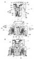
図1は、本発明の一実施形態としてのプラグ側コネクタ(以下「第一コネクタ」という)とこれに嵌合接続されるレセプタクル側コネクタ(以下「第二コネクタ」という)と、有するコネクタ組立体であり、図1(A)は嵌合接続前、そして図1(B)は嵌合接続後の状態をそれぞれ示す外観斜視図である。ここで、プラグ側とは雄型の端子を、レセプタクル側とはこれに嵌合する雌型の端子を有する側を示している。また、図2は図1の両コネクタの内部を示すように断面された斜視図であり、図2(A)は図1(A)に対応する嵌合接続前、図2(B)は図1(B)に対応する嵌合接続後の状態を示している。さらには、図3は上記プラグ側コネクタたる第一コネクタを単体で示しており、図3(A)は外観斜視図、(B)は断面斜視図である。そして図4は上記レセプタクル側コネクタたる第二コネクタを単体で示しており、図4(A)は外観斜視図、図4(B)は断面斜視図である。 FIG. 1 shows a connector assembly having a plug-side connector (hereinafter referred to as “first connector”) and a receptacle-side connector (hereinafter referred to as “second connector”) fitted and connected thereto as an embodiment of the present invention. FIG. 1A is an external perspective view showing a state before fitting connection, and FIG. 1B is a state after fitting connection. Here, the plug side indicates a male terminal, and the receptacle side indicates a side having a female terminal fitted therein. 2 is a perspective view of the inside of both connectors shown in FIG. 1, and FIG. 2 (A) is a pre-fitting connection corresponding to FIG. 1 (A), and FIG. The state after the fitting connection corresponding to 1 (B) is shown. 3 shows the first connector as the plug-side connector as a single unit, FIG. 3A is an external perspective view, and FIG. 3B is a cross-sectional perspective view. 4 shows the second connector as the receptacle-side connector alone, FIG. 4 (A) is an external perspective view, and FIG. 4 (B) is a cross-sectional perspective view.
第一コネクタ1は、雄型の第一端子(第一コネクタを構成する端子そしてハウジングには「第一」を付すこととし、第二コネクタ2については「第二」を付すこととする。)10と該第一端子10を保持する電気絶縁材製の第一ハウジング20とを有している。該第一ハウジング20は、回路基板(図示せず)に対し第一端子10を介し取り付けられる固定ハウジング21と該固定ハウジング21に対して可動な可動ハウジング26とを有している。上記第一コネクタ1は、その第一ハウジング20が回路基板に平行な面で長手方向と短手方向に延び略直方体外形をなしていて、該第一ハウジング20の長手方向に二列をなして上記第一端子10が配列されている。二列の第一端子10は、上記長手方向に対して直角な短手方向(コネクタ幅方向)で互いに対称な向きで対向している。 The
固定ハウジング21は、回路基板に対し垂立し長手方向に延びる側壁22と短手方向に延びる端壁23とで周壁24を形成し、該周壁24の内方は上下に貫通していて上方から可動ハウジング26を収める中央空間24Aを形成している。上記側壁22は、長手方向にて端子配列範囲にわたり、外壁面に第一端子10の保持のための突出壁22Aが設けられ、該側壁22の内壁面は内方そして下方に向け開口された固定側凹部22Bが形成されている。該固定側凹部22Bは、後述の第一端子10の弾性部を収める収容空間の一部を形成する。上記突出壁22Aそして固定側凹部22Bについては、後に第一端子10との関連で詳述する。 The fixed
上記固定ハウジング21の端壁23には、その外面位置にL型の取付金具30が設けられていて、該取付金具30に形成された取付孔31にて半田により回路基板に強固に固定取付される。なお、該取付金具30は固定ハウジング21の回路基板への取付けに際し、必須なものではなく、上記第一端子10の回路基板への半田接続による取付強度が十分確保できるときには、該取付金具30は不要である。 The
可動ハウジング26は、上記固定ハウジング21の中央空間24A内に貫入して位置する貫入部26Aと、上記中央空間24Aから上方へ突出して位置する突出部26Bとを有している。該可動ハウジング26は、上記突出部26Bから貫入部26Aに及ぶ範囲に相手接続部材、例えば相手コネクタとしての第二コネクタを受け入れる受入凹部27が上方に開口して形成されている。該受入凹部27内には、可動ハウジング26の底壁29から立ち上がる第一端子10の保持のための中央突壁29Aが設けられている。さらに、可動ハウジング26の貫入部26Aの外面には、上記固定ハウジング21の固定側凹部21Bに対向するように可動側凹部26Cが下方に開口して形成されている。該可動側凹部26Cは上記固定側凹部22Bとともに、後述の第一端子10の上記弾性部を収容する収容空間20Aを形成する。 The
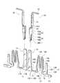
雄端子をなす第一端子10は、図5に見られるように、金属板の平坦面を維持したまま形状づけられている。この第一端子10は、同一形状の端子がコネクタ幅方向で左右対称となるようにして同方向で対向して対をなして配置されており、コネクタ長手方向で複数対が配列されている。図5では、複数対の第一端子10のうち、一対のみが第一ハウジング20から抽出された状態で、これらに接続される相手コネクタとしての第二コネクタ2の一対の第二端子40とともに図示されている。対をなして図示されている二つの第一端子10は、左右対称に配置されてはいるものの同一形状であるので、以下、一方の第一端子10について説明する。 As can be seen in FIG. 5, the
第一端子10は、コネクタ幅方向で対向する相手方となる第二端子40に近接する位置で垂立し可動ハウジング26により保持される可動側柱部11と、該可動側柱部11に対し上記コネクタ幅方向で、反対側に位置して垂立する固定側柱部12と、固定側柱部12の下端から横方向に延びる接続部13と、可動側柱部11と固定側柱部12の間に位置する弾性部14とを一体に有している。 The
上記可動側柱部11は、その上半部が第二コネクタ2の雌型の第二端子40と接触する接触部11Aをなし、下半部が可動ハウジング26に固定保持される可動側被保持部11Bをなしている。接触部11Aはその先端(上端)が上記第二端子40への嵌入を容易とするように面取りされており、可動側被保持部11Bは可動ハウジング26に係止するためにその側縁に係止突起11B−1が設けられている。 The movable
上記可動側被保持部11Bは、可動ハウジング26の底壁29に形成された保持溝29Bに下方から圧入されて該保持溝29Bで保持される(図3(B)参照)。その際、上記係止突起11B−1が該保持溝29Bの対応内面に喰い込み係止が強固になる。 The movable side held
上記固定側柱部12は、その下端側の基部12Aよりも上方部分が固定側被保持部12Bとして形成されている。該固定側被保持部12Bには、固定ハウジング21に係止するための係止突起12B−1が設けられている。該固定側被保持部12Bは、固定ハウジング21の側壁22の底壁面で突出した突出壁22Aの厚み内に上下貫通して形成された保持溝22A−1に下方から圧入されて該保持溝22A−1で保持される。その際、上記係止突起12B−1が該保持溝22A−1の対応内面に喰い込み係止が強固になる。 The fixed
上記固定側柱部12の基部12Aの下端からは固定ハウジング21の下面に沿って横方向に延び固定ハウジング21外へ向け突出する接続部13が設けられている。 A connecting
上記第一端子10は、上記可動側被保持部11Bと固定側被保持部12Bとの間に位置する部分に弾性部14を有している。該弾性部14は、左方へは、上記可動側被保持部11Bの下端から横方向に延びる可動側移行部15を経て上記可動側被保持部11Bと連結され、右方へは、上記固定側被保持部12Bの下方の基部12Aから横方向に延びる固定側移行部16を経て上記固定側被保持部12Bに連結されている。 The
上記弾性部14は、上記可動側移行部15と固定側移行部16とから立ち上がり、略M字状をなして屈曲されて一つの連続した帯状部をなしている。略M字状をなす該弾性部14は、可動側被保持部11Bそして固定側被保持部12Bよりも細い幅の帯状をなしており、上部に弯曲形状の二つの屈曲部14A,14Cと下部に弯曲形状の一つの屈曲部14Bを有するとともに、屈曲部14Aと屈曲部14Bを結ぶ内側直状部14Dそして屈曲部14Cと屈曲部14Bを結ぶ内側直状部14E、さらには、上記屈曲部14Aと屈曲部14Cのそれぞれから外側に延びる外側直状部14F,14Gを有し、二つの逆U字状の波形部の間に一つのU字状の波形部を位置させて全体として略M字状をなすように三つの波形部を連続した波形をなしていて弾性変形を可能としている。かくして、三つの波形部のそれぞれは、屈曲部と直状部とを有している。三つの波形部において、各直状部14D,14E,14F,14Gは、屈曲部14Aと14Cあるいは14Bから遠くになるにしたがい波形の開き幅を広くするように傾斜した拡幅部分を形成している。 The
上記三つの波形部のうち、左側に位置する波形部は、外側直状部14Fから下方に延びて上下方向で屈曲部14Bよりも下方位置で下方に向け内側(図5にて右側)に傾斜する傾斜部14Hを有しており、これに対し、右側に位置する波形部は、上記外側直状部14Gから下方に延びて下方の屈曲部14Bよりも下方位置で下方に向け内側(図5にて左側)に傾斜する傾斜部14Iを有している。かくして、上記傾斜部14Hと傾斜部14Iとが、下方に向け内側に傾斜することで、上記下方の屈曲部14Bよりも下方の範囲で、互いの間隔を狭めている。 Of the three corrugated parts, the corrugated part located on the left side extends downward from the outer
弾性部14は、細い幅の帯状で弾性を得るように波形をなしているが、本実施形態では、各直状部14D,14E,14F,14Gの中央部分にかけて屈曲部14A、14Cよりも除々に端子幅(帯幅)が狭くなっていて、また、内側直状部14D,14Eの中央部分にかけて屈曲部14Bよりも除々に端子幅(帯幅)が狭くなっている。また、弾性部14は外側直状部14F,14Gの中央部分にかけて傾斜部14H、14Iよりも除々に端子幅(帯幅)が狭くなっている。なお、該弾性部14は、除々に端子幅(帯幅)が狭くなっていればよく、中央部分の位置は問わない。かくして、上記弾性部14は、屈曲部を支点として弾性撓み変形を生じやすくしている。 The
次に、第二コネクタ2は、図1,2,4に見られるように、雌型の第二端子40と該第二端子40を保持する電気絶縁材製の第二ハウジング50を有し、該第二ハウジング50が回路基板(図示せず)に対し上記第二端子40を介して取り付けられている。該第二ハウジング50は、第一コネクタ1の第一ハウジング20における長手方向そして短手方向をそれぞれ該第二ハウジング50の長手方向そして短手方向とする略直方体外形をなしていて、該第二ハウジング50の長手方向に二列をなして上記第二端子40が配列されている。二列の第二端子40は、上記長手方向に対して直角な短手方向(コネクタ幅方向)で互いに対向している。なお、図1及び図2では、上記第二コネクタ2は第一コネクタ1に対する嵌合方向を向く姿勢で示されているが、第二コネクタ2単体を示す図4では、上下方向で反転した姿勢で描かれている。 Next, as shown in FIGS. 1, 2, and 4, the
第一コネクタ1の相手方たる第二コネクタ2の第二ハウジング50は、回路基板(図示せず)に対して取り付けられる取付ブロック部51と、該取付ブロック部51から第一コネクタ1への嵌合方向に突出する嵌合ブロック部52とを有し、ともに第一コネクタ1の長手方向そして短手方向をそれぞれ同じく長手方向そして短手方向とする略直方体外形をなしている。上記第二ハウジング50は、図1そして図2で上方から見て取付ブロック51の中央で、上部側に上部没入部53Aそして下部側に上部没入部53Aよりも幅狭で深い下部没入部53Bが形成されていて、該上部没入部53Aと下部没入部53Bの間の部分に、中央壁部54が形成されており、上記上部没入部53Aと下部没入部53Bの内壁に沿って延び上記中央壁部54を貫通する端子溝55が形成されている。該端子溝55には後に詳述する第二端子40が圧入保持されている。 The
上記取付ブロック部51の長手方向に延びる側壁56の外面(図4(A)参照)は、該長手方向中央部にて、短手方向に没した凹壁部56Aが形成されていて、ここに後に詳述する第二端子40の接続部42が位置しており、回路基板へのこの接続部42の半田接続そしてその接続確認を容易としている。 On the outer surface of the
上記第二ハウジング50の端壁57には、その外面位置にL型の取付金具60が設けられていて、該取付金具60に形成された取付孔61にて半田により回路基板に強固に固定取付される。なお、該取付金具60は第二ハウジング50の回路基板への取付けに際し、必須なものではなく、上記第二端子40の回路基板への半田接続による取付強度が十分確保できるときには、該取付金具60は不要である。 The
雌端子をなす第二端子40は、既述の第一端子10と対応してコネクタ嵌合接続前の状態を示す図5に見られるように、金属帯状部材を板厚方向に屈曲して形状づけられている。この第二端子40は、第一端子10と同様に同一形状の端子がコネクタ幅方向で左右対称となるようにして同方向で対向して対をなして配置されており、コネクタ長手方向で複数対が配列されている。図5では、複数対の第二端子40のうち、一対のみが第二ハウジング50から抽出された状態で図示されている。対をなして図示されている二つの第二端子40は、左右対称に配置されてはいるものの同一形状であるので、以下、一方の第二端子40について説明する。 The
上記第二端子40は、図5にて、該第二端子40の中間部の位置で上記第一端子10の板面に対し直角方向な板面をなす平帯状の被保持部41と、該被保持部41よりも上端側で該被保持部41の板面に対して直角に屈曲された接続部42と、上記被保持部41よりも下方での中間位置に断面がU字状をなす中間基部43と、該中間基部43よりもさらに下側で、フィンガ状に延びる一対の接触片44Aから成る接触部44とを有している。 The
上記被保持部41は平帯状をなし両側縁には、第二ハウジング50の端子溝55の対応面に喰い込む係止突起41Aが設けられている。 The held
上記被支持部43は、くびれた連結部45を介して上記被保持部41と連結されており、上記被保持部41の板面を下方に延長した板面状の底面部43Aと、該底面部43Aの両側縁から該底面部の板面に対して直角をなす側面部43Bを有し、上記底面部43Aと両側の側面部43BとでU字状をなしている。 The supported
上記接触部44は、上記中間基部43の両側の側面部43Bの下端からそれぞれ下方へ向けフィンガ状に延びる一対の接触片44Aを対向させることで形成されている。この一対の接触片44Aは下方に向けその間隔を次第に狭めて互いに近接する方向に傾斜し、下端近傍で上記間隔を最小とし、再び下端に向け広がり、この間隔が最小の部分で喉部44A−1を形成している。該喉部44A−1における両接触片44Aの間隔は既述の第一端子10の接触部11Aの板厚よりも小さく、上記喉部44A−1で該接触部11Aを挟圧して弾性接触するようになっている。 The
かかる形状の第二端子40は、図1そして図2において第二ハウジング50の端子溝55へ上方から圧入される(第二コネクタ2を図1,2に対して上下反転して示す図4にあっては下方から圧入される)。上記端子溝55は、図2(A)において、上記第二端子40が上方から圧入される関係上、上記中央壁部54には、上記第二端子40の最大外周形、すなわち、断面がU字状をなす中間基部43の外周形状に相当する内周形状の四角筒孔54Aが該中央壁部54を上下に貫通して形成されていて、上記中間基部43の通過を可能としている。一方、四角筒孔54A及び上部没入部53Aの内壁面には、上記断面がU字状の中間基部43が上記中央壁部54の上記四角筒孔54Aを通過した後に、該上部没入部53Aの内壁面に位置する平帯状の被保持部41を収める溝部55Aが該被保持部41の板厚に相当する深さの溝として形成されており、被保持部41の係止突起41Aが該被保持部41の溝部55Aへの圧入の際、この溝部55Aの内面へ喰い込んで、第二ハウジング50により保持され抜けが防止される。また、上記中央壁部54よりも下方(図4では上方)の下部没入部53Bの内壁面には上記第二端子40を所定位置に圧入組立てされた際に上記中間基部43と接触部44とを収める溝部55Bが形成されている。上記溝部55Bは、上記中間基部43に対しては、該溝部55Bの溝底面が上記中間基部43の底面部43Aと接触しあるいは間隙を形成し、溝側面が側面部43Bに対し間隙を形成しており、また接触部44に対しては、一対の接触片44Aの弾性変形を可能とする空間を形成している。 The
かかる構成の本実施形態の回路基板用電気コネクタの使用要領を、主として図1、図2にもとづき以下に説明する。 The usage point of the circuit board electrical connector of this embodiment having such a configuration will be described below mainly based on FIGS.
第一コネクタ1と第二コネクタ2は、それぞれ対応する回路基板へ半田接続により取り付けられる。すなわち、第一コネクタ1は、固定ハウジング21に保持されている第一端子10の接続部13と取付金具30とで半田され、第二コネクタ2は第二端子40の接続部42と取付金具60とで半田されることで、それぞれ回路基板へ取り付けられる。図1、図2では、回路基板は図示が省略されているが、第一コネクタ1はその下面でそして第二コネクタ2はその上面で回路基板に取り付けられている。 The
先ず、図1(A)そして図2(A)に見られるように、上面で回路基板に取り付けられている第二コネクタ2が、その嵌合ブロック部52を下向きとした姿勢で、上記第一コネクタ1の上方位置にもたらされる。しかる後、上記第二コネクタ2はそのままの姿勢で降下され、上記嵌合ブロック部52が第一コネクタ1の可動ハウジング26の受入凹部27へ進入し該可動ハウジング26に嵌合される(図1(B)、図2(B)参照)。 First, as can be seen in FIGS. 1A and 2A, the
第二コネクタ2が第一コネクタ1に嵌合されると、第二コネクタ2の第二端子40は対をなすフィンガ状の接触片44Aから成る接触部44が第一コネクタ1の第一端子10の接触部11Aを挟圧して該接触部11Aと弾性接触するようになる。 When the
上記第二端子40の接触部44は、対をなす接触片44Aの下端近傍に喉部44A−1を有しているので、この喉部44A−1へ第一端子10の平帯状の接触部11Aが円滑に進入することで、該第一端子10の接触部11Aを弾性力をもって挟圧して該第一端子10との電気的接続がなされる。 Since the
かくして、第一コネクタ1と第二コネクタ2とは接続され、第一コネクタ1側の回路基板と第二コネクタ2側の回路基板は、第一端子10そして第二端子40を介して導通状態となる。 Thus, the
上記第一コネクタ1の第一端子10は弾性部14を有しており、第二コネクタ2が正規位置あるいは正規姿勢からコネクタ長手方向、短手方向、挿抜方向で多少ずれていてもあるいは両コネクタ1,2の少なくとも一方が振動を受けても、上記弾性部14でそのずれあるいは振動を吸収する。さらには、上記弾性部14に加え、第一端子10の接触部11Aが平帯状であるので、これを挟圧する接触部44はその喉部44A−1が上記接触部11Aの板面との間でコネクタ短手方向及び挿抜方向での摩擦を伴うものの該板面に沿って上記接触部11Aに対して相対変位(移動)が可能であり、この相対変位によっても上記ずれや振動を吸収する。 The
上記弾性部14の挙動についてさらに詳述すると、上記第一端子10は、可動ハウジング26により保持されている可動側被保持部11Bと固定ハウジング21により保持されている固定側被保持部12Bとの間に、可動側移行部15と固定側移行部16のそれぞれを介して上記可動側被保持部11Bと固定側被保持部12Bに接続する弾性部14を有している。この弾性部14は上記可動側移行部15と固定側移行部16から立ち上がり略M字状の波形をなしており、コネクタ高さ方向、コネクタ長手方向そして短手方向(コネクタ幅方向)のいずれの方向にも弾性変位可能となっているので、したがって、第一コネクタ1と第二コネクタ2とが、上記のいずれの方向にずれても、あるいは振動を受けても、これを吸収する。 The behavior of the
波形をなす上記弾性部14は、直状部14D,14E,14F,14Gが傾斜していて中央のU字状そして両側の逆U字状をなす各波形部で、屈曲部14B,14A,14Cから離れるにしたがい波形の開き幅を大きくする拡幅部分を形成しているので、上記コネクタ幅方向で、該弾性部14が可動ハウジング26と固定ハウジング21からコネクタ幅方向に圧縮されたとき、各波形部が互いに近接しても当接しにくくなりそれだけ弾性変位量が大きく確保される。上記弾性部14は、図示されているごとく、すべての直状部で傾斜させて各波形部にて拡幅部分が形成されているようにしてもよいが、少なくとも、両方の外側に位置する可動側被保持部と固定側被保持部にそれぞれ隣接している波形部について拡幅部分が形成されていれば十分であり、中間に位置する波形部は傾斜せずに拡幅部分を有していなくてもよい。 The
さらには、両方の外側の直状部14F,14Gは、コネクタ幅方向で中央に位置する下側の屈曲部14Bよりも下方位置で互いにコネクタ幅方向で互いに近づくように傾斜した傾斜部14H,14Iを介してそれぞれ可動側移行部15そして固定側移行部16と接続されているので、可動側移行部15と固定側移行部16との間では波形部は不存在であり、上記弾性部14がコネクタ幅方向で圧縮される弾性変位を生じて上記可動側移行部15と固定側移行部16とが大きく近づいても両者が当接することはない。 Furthermore, the outer
また、本実施形態では、直状部14D,14E、14F,14Gが屈曲部14A,14B,14Cよりも帯幅が小さくなっているので、該屈曲部14A,14B,14Cを支点として撓みを生じやすくなっており、直状部14D,14E、14F,14Gを可能な限り長く、すなわち波の高さを大きくすることで、弾性部14の弾性変位量を、コネクタ高さ方向、コネクタ長手方向(弾性部の板面に対し直角方向)、コネクタ短手方向(コネクタ幅方向)のいずれかの方向でも大きく確保できる。また、屈曲部14A,14B,14Cよりも直状部14D,14E,14F,14Gの帯幅が小さいので、撓みが生じた際に屈曲部に掛かる応力を直状部14D,14E、14F,14Gに分散させることによって、屈曲部同士14A,14C、または、屈曲部14Bと直状部14F,14G、または、隣り合う直状部同士が弾性変位時に互いに当接しにくくなる。また、上記弾性部14は、図示されているごとく、すべての直状部において直状部の中央部分にかけて除々に端子幅(帯幅)が狭くなっているようにしてもよいが、少なくとも、いずれかの屈曲部と直状部においてから除々に端子幅(帯幅)が狭くなっているように形成されていれば十分であり、他の屈曲部と直状部はこのような端子幅(帯幅)を有していなくてもよい。 In the present embodiment, the
本発明は、図示された形態のような二つのコネクタのそれぞれが接続される回路基板同士を平行とする場合のみならず、例えば、互いに直角をなす、いわゆるライトアングルのコネクタにも適用可能である。 The present invention is applicable not only to the case where the circuit boards to which each of the two connectors as shown in the figure are connected are parallel to each other, but also to a so-called right angle connector that is perpendicular to each other, for example. .
1 (第一)コネクタ 14 弾性部
2 相手接続部材(第二コネクタ) 14A〜C 屈曲部
10 (第一)端子 14D〜G 直状部
11A 接触部 20 ハウジング
11B 可動側被保持部 20A 収容空間
12B 固定側被保持部 21 固定ハウジング
13 接続部 26 可動ハウジングDESCRIPTION OF SYMBOLS 1 (1st)
Claims (5)
Translated fromJapanese上記端子は、固定ハウジングで保持される固定側被保持部と、可動ハウジングで保持されコネクタ幅方向で上記固定側被保持部と距離をもって位置する可動側被保持部と、固定側被保持部と可動側被保持部を連結していて弾性変形可能な弾性部とを有し、
上記ハウジングは、固定ハウジングと可動ハウジングとの間に、上記端子の弾性部を収容する収容空間を形成し、
上記弾性部は、一つの連続した帯状部をなすとともに、屈曲方向を繰り返して反転し、上記回路基板側に位置する下方の屈曲部と上記相手接続部材側に位置する上方の屈曲部との複数の屈曲部を経て波形部を連続して形成しているとともに、固定側被保持部と可動側被保持部に隣接するそれぞれの波形部が上方の屈曲部から下方に延びて波形の開き幅を、上記上方の屈曲部から離れ下方に向うにしたがい、広くしている拡幅部分を形成し、該拡幅部分の下端から上記下方の屈曲部よりも下方に延びる延長部が設けられていることを特徴とする回路基板用電気コネクタ。The terminal has a connection part for connecting to the circuit board on one end side and a contact part for contacting the mating connection member on the other end side, and a housing for holding the terminal is connected to the circuit board via the terminal. In an electrical connector for a circuit board having a fixed housing for mounting and a movable housing movable with respect to the fixed housing, and the mating connecting member is fitted into the movable housing,
The terminal includes a fixed-side held portion which is held in a fixed housing, and the movable held partin the connector width direction are held by the movable housingyou position with the distance and the fixed-side held part, the fixed-side held part And an elastic part that is elastically deformable by connecting the movable side held part,
The housing forms an accommodating space for accommodating the elastic portion of the terminal between the fixed housing and the movable housing,
The elastic portion forms one continuous band-like portion, and reverses the bending direction repeatedly,and includes a plurality of lower bent portions located on the circuit board side and upper bent portions located on the counterpart connection member side. The corrugated portion is formed continuously through the bent portion, and the corrugated portions adjacent to the fixed side held portion and the movable side held portionextend downward from the upper bent portion to increase the opening widthof the corrugatedportion. , characterized in that following thedirected downwardly away from theupper bent portion, the widened portionis formedwidely, the extension extending downward from the bent portion of the downwardly from the lower end of the enlarged width portion isprovided An electrical connector for circuit boards.
Priority Applications (4)
| Application Number | Priority Date | Filing Date | Title |
|---|---|---|---|
| JP2015244322AJP6438382B2 (en) | 2015-12-15 | 2015-12-15 | Circuit board electrical connector |
| US15/364,400US10062995B2 (en) | 2015-12-15 | 2016-11-30 | Electrical connector |
| CN201611102268.1ACN107026335B (en) | 2015-12-15 | 2016-12-05 | Electrical connectors for circuit boards |
| EP16020483.0AEP3182523B1 (en) | 2015-12-15 | 2016-12-06 | Electrical connector |
Applications Claiming Priority (1)
| Application Number | Priority Date | Filing Date | Title |
|---|---|---|---|
| JP2015244322AJP6438382B2 (en) | 2015-12-15 | 2015-12-15 | Circuit board electrical connector |
Related Child Applications (1)
| Application Number | Title | Priority Date | Filing Date |
|---|---|---|---|
| JP2016247694ADivisionJP6356775B2 (en) | 2016-12-21 | 2016-12-21 | Electrical connector assembly |
Publications (2)
| Publication Number | Publication Date |
|---|---|
| JP2017111918A JP2017111918A (en) | 2017-06-22 |
| JP6438382B2true JP6438382B2 (en) | 2018-12-12 |
Family
ID=57517675
Family Applications (1)
| Application Number | Title | Priority Date | Filing Date |
|---|---|---|---|
| JP2015244322AActiveJP6438382B2 (en) | 2015-12-15 | 2015-12-15 | Circuit board electrical connector |
Country Status (4)
| Country | Link |
|---|---|
| US (1) | US10062995B2 (en) |
| EP (1) | EP3182523B1 (en) |
| JP (1) | JP6438382B2 (en) |
| CN (1) | CN107026335B (en) |
Cited By (1)
| Publication number | Priority date | Publication date | Assignee | Title |
|---|---|---|---|---|
| US12394928B2 (en) | 2022-02-03 | 2025-08-19 | Hirose Electronic Co., Ltd. | Circuit board electrical connector |
Families Citing this family (28)
| Publication number | Priority date | Publication date | Assignee | Title |
|---|---|---|---|---|
| JP6727103B2 (en)* | 2016-11-11 | 2020-07-22 | ヒロセ電機株式会社 | Electrical connector for circuit board and manufacturing method thereof |
| JP6480500B2 (en)* | 2017-04-28 | 2019-03-13 | 日本航空電子工業株式会社 | connector |
| US10608361B2 (en)* | 2017-05-19 | 2020-03-31 | Molex, Llc | Connector and connector assembly |
| JP7184996B2 (en)* | 2017-07-11 | 2022-12-06 | イリソ電子工業株式会社 | connector |
| JP6415654B1 (en)* | 2017-07-28 | 2018-10-31 | イリソ電子工業株式会社 | Electronic components |
| JP6851937B2 (en)* | 2017-08-09 | 2021-03-31 | ヒロセ電機株式会社 | Electrical connector for circuit board and its manufacturing method |
| JP6446109B1 (en) | 2017-10-10 | 2018-12-26 | イリソ電子工業株式会社 | connector |
| US10096914B1 (en)* | 2017-11-16 | 2018-10-09 | Greenconn Corp. | Floating connector and conductive terminal thereof |
| JP6400818B1 (en)* | 2017-11-17 | 2018-10-03 | イリソ電子工業株式会社 | Movable connector |
| WO2019146589A1 (en)* | 2018-01-24 | 2019-08-01 | パナソニックIpマネジメント株式会社 | Electronic device |
| JP6959876B2 (en)* | 2018-01-25 | 2021-11-05 | 日本航空電子工業株式会社 | connector |
| CN207743489U (en)* | 2018-01-30 | 2018-08-17 | 奥克斯空调股份有限公司 | Termination and air-conditioning |
| JP6971182B2 (en)* | 2018-03-23 | 2021-11-24 | 京セラ株式会社 | Connectors and electronics |
| JP6979380B2 (en)* | 2018-03-23 | 2021-12-15 | 京セラ株式会社 | Connectors and electronics |
| JP6598912B2 (en)* | 2018-03-26 | 2019-10-30 | 京セラ株式会社 | Connectors and electronic devices |
| JP7197995B2 (en)* | 2018-04-26 | 2022-12-28 | ヒロセ電機株式会社 | electrical connector for circuit board |
| KR102611241B1 (en)* | 2018-07-17 | 2023-12-06 | 엘에스엠트론 주식회사 | Receptacle connector and plug connector |
| JP7077177B2 (en) | 2018-08-08 | 2022-05-30 | 日本航空電子工業株式会社 | connector |
| CN111541071B (en)* | 2019-02-07 | 2024-03-15 | 泰科电子日本合同会社 | Connector assembly |
| CN109950716B (en)* | 2019-04-25 | 2024-02-06 | 苏州祥龙嘉业电子科技股份有限公司 | Floating BTB connector |
| JP7341842B2 (en)* | 2019-10-15 | 2023-09-11 | ヒロセ電機株式会社 | Connector assembly method, in-vehicle equipment assembly method, connector assembly, in-vehicle equipment |
| CN111326878A (en)* | 2020-02-28 | 2020-06-23 | 广州正业电子科技股份有限公司 | Electrical connector |
| JP7369666B2 (en) | 2020-05-15 | 2023-10-26 | ヒロセ電機株式会社 | electrical connector for circuit board |
| CN112882968A (en)* | 2021-01-19 | 2021-06-01 | 凯晖科技股份有限公司 | Floating plug-in computer equipment |
| US11621514B2 (en)* | 2021-05-28 | 2023-04-04 | Te Connectivity Solutions Gmbh | Electrical connector with connector housing joined by a flexible joining member |
| CN114039234B (en)* | 2021-10-28 | 2023-10-20 | 上海航天科工电器研究院有限公司 | Floating electric connection conductor structure, floating electric connector and vehicle-mounted electronic device |
| JP7732918B2 (en)* | 2022-02-03 | 2025-09-02 | ヒロセ電機株式会社 | Electrical Connectors for Circuit Boards |
| JP2023138067A (en) | 2022-03-18 | 2023-09-29 | イリソ電子工業株式会社 | connector |
Family Cites Families (21)
| Publication number | Priority date | Publication date | Assignee | Title |
|---|---|---|---|---|
| JP3016164B2 (en)* | 1991-06-19 | 2000-03-06 | 日本エー・エム・ピー株式会社 | Movable connector |
| JP3228460B2 (en)* | 1996-08-08 | 2001-11-12 | ヒロセ電機株式会社 | Floating electrical connector |
| JP2004214092A (en)* | 2003-01-07 | 2004-07-29 | Jst Mfg Co Ltd | Reinforcing tab for movable connector and movable connector using the same |
| JP2004214091A (en)* | 2003-01-07 | 2004-07-29 | Jst Mfg Co Ltd | Contact for movable connector and movable connector using the same |
| JP3905518B2 (en)* | 2004-01-23 | 2007-04-18 | ケル株式会社 | Floating connector |
| JP2006120448A (en)* | 2004-10-21 | 2006-05-11 | Sony Corp | Mounting structure for connector |
| TWI318483B (en)* | 2006-04-28 | 2009-12-11 | I Pex Co Ltd | Electrical connector |
| JP5135015B2 (en)* | 2008-03-21 | 2013-01-30 | 第一電子工業株式会社 | Electrical connector |
| JP5603790B2 (en)* | 2011-01-28 | 2014-10-08 | ケル株式会社 | Floating connector |
| DE102012016281B4 (en)* | 2012-08-17 | 2016-03-31 | Wago Verwaltungsgesellschaft Mbh | Electrical connection arrangement and its components |
| CN104584331B (en)* | 2012-09-05 | 2017-02-22 | 意力速电子工业株式会社 | Connector |
| JP5296915B1 (en)* | 2012-11-15 | 2013-09-25 | イリソ電子工業株式会社 | Electrical connection terminal and connector provided with the same |
| EP2733793B1 (en)* | 2012-11-15 | 2016-06-15 | Iriso Electronics Co., Ltd. | Electric connection terminal and connector including the same |
| JP5491664B1 (en)* | 2013-07-19 | 2014-05-14 | イリソ電子工業株式会社 | Electrical connector |
| JP6116056B2 (en)* | 2013-08-07 | 2017-04-19 | 日本航空電子工業株式会社 | connector |
| JP5481595B1 (en)* | 2013-08-20 | 2014-04-23 | イリソ電子工業株式会社 | Electrical connector |
| TWI525920B (en) | 2013-09-05 | 2016-03-11 | 意力速電子工業股份有限公司 | Connector |
| JP3192828U (en)* | 2014-06-20 | 2014-09-04 | イリソ電子工業株式会社 | Electrical connector |
| TWI614947B (en)* | 2013-11-13 | 2018-02-11 | Iriso Electronics Co Ltd | Electrical connector |
| JP6553843B2 (en)* | 2014-03-18 | 2019-07-31 | 日本航空電子工業株式会社 | connector |
| DE112015001539T5 (en)* | 2014-06-23 | 2016-12-22 | Iriso Electronics Co., Ltd. | Connection structure of a connector and connector |
- 2015
- 2015-12-15JPJP2015244322Apatent/JP6438382B2/enactiveActive
- 2016
- 2016-11-30USUS15/364,400patent/US10062995B2/enactiveActive
- 2016-12-05CNCN201611102268.1Apatent/CN107026335B/enactiveActive
- 2016-12-06EPEP16020483.0Apatent/EP3182523B1/enactiveActive
Cited By (1)
| Publication number | Priority date | Publication date | Assignee | Title |
|---|---|---|---|---|
| US12394928B2 (en) | 2022-02-03 | 2025-08-19 | Hirose Electronic Co., Ltd. | Circuit board electrical connector |
Also Published As
| Publication number | Publication date |
|---|---|
| EP3182523A1 (en) | 2017-06-21 |
| EP3182523B1 (en) | 2024-04-24 |
| US20170170588A1 (en) | 2017-06-15 |
| US10062995B2 (en) | 2018-08-28 |
| JP2017111918A (en) | 2017-06-22 |
| CN107026335B (en) | 2019-07-26 |
| CN107026335A (en) | 2017-08-08 |
Similar Documents
| Publication | Publication Date | Title |
|---|---|---|
| JP6438382B2 (en) | Circuit board electrical connector | |
| JP6446392B2 (en) | Connection structure between circuit board electrical connector and mating connection member | |
| CN112510404B (en) | Electrical connector for circuit board | |
| KR101639801B1 (en) | Connector | |
| JP6068405B2 (en) | Electrical connector assembly | |
| CN109802258B (en) | Electric connector and combination thereof | |
| JP2010040309A (en) | Electrical connector with multi-contact terminal | |
| JP6883305B2 (en) | Electrical connector assembly | |
| EP4224637A1 (en) | Circuit board electrical connector | |
| JP6356775B2 (en) | Electrical connector assembly | |
| CN103825134B (en) | Circuit board electric connector | |
| JP2017111931A (en) | Electrical connector for board connection | |
| JP5701915B2 (en) | Electrical connector with multi-contact terminals | |
| JP6279967B2 (en) | Connecting terminal | |
| JP2011165682A (en) | Electric connector with multi-contact terminal | |
| CN100511869C (en) | Electrical connector having ground planes | |
| JP6934095B2 (en) | Electrical connector for circuit board | |
| JP7732918B2 (en) | Electrical Connectors for Circuit Boards | |
| KR102539251B1 (en) | Contacts for direct plug-in connectors, and direct plug-in connectors | |
| JP2023111294A (en) | Floating Connectors, Board-to-Board Connectors and Terminals | |
| JP2024127273A (en) | Electrical Connectors for Circuit Boards | |
| JP2008097851A (en) | Electrical connector |
Legal Events
| Date | Code | Title | Description |
|---|---|---|---|
| A621 | Written request for application examination | Free format text:JAPANESE INTERMEDIATE CODE: A621 Effective date:20170728 | |
| A977 | Report on retrieval | Free format text:JAPANESE INTERMEDIATE CODE: A971007 Effective date:20180529 | |
| A131 | Notification of reasons for refusal | Free format text:JAPANESE INTERMEDIATE CODE: A131 Effective date:20180531 | |
| A521 | Request for written amendment filed | Free format text:JAPANESE INTERMEDIATE CODE: A523 Effective date:20180726 | |
| TRDD | Decision of grant or rejection written | ||
| A01 | Written decision to grant a patent or to grant a registration (utility model) | Free format text:JAPANESE INTERMEDIATE CODE: A01 Effective date:20181102 | |
| A61 | First payment of annual fees (during grant procedure) | Free format text:JAPANESE INTERMEDIATE CODE: A61 Effective date:20181116 | |
| R150 | Certificate of patent or registration of utility model | Ref document number:6438382 Country of ref document:JP Free format text:JAPANESE INTERMEDIATE CODE: R150 | |
| S531 | Written request for registration of change of domicile | Free format text:JAPANESE INTERMEDIATE CODE: R313531 | |
| R350 | Written notification of registration of transfer | Free format text:JAPANESE INTERMEDIATE CODE: R350 | |
| R250 | Receipt of annual fees | Free format text:JAPANESE INTERMEDIATE CODE: R250 | |
| R250 | Receipt of annual fees | Free format text:JAPANESE INTERMEDIATE CODE: R250 | |
| R250 | Receipt of annual fees | Free format text:JAPANESE INTERMEDIATE CODE: R250 | |
| R250 | Receipt of annual fees | Free format text:JAPANESE INTERMEDIATE CODE: R250 |