JP6434872B2 - Semiconductor device - Google Patents
Semiconductor deviceDownload PDFInfo
- Publication number
- JP6434872B2 JP6434872B2JP2015152626AJP2015152626AJP6434872B2JP 6434872 B2JP6434872 B2JP 6434872B2JP 2015152626 AJP2015152626 AJP 2015152626AJP 2015152626 AJP2015152626 AJP 2015152626AJP 6434872 B2JP6434872 B2JP 6434872B2
- Authority
- JP
- Japan
- Prior art keywords
- layer
- semiconductor layer
- semiconductor
- semiconductor device
- orientation
- Prior art date
- Legal status (The legal status is an assumption and is not a legal conclusion. Google has not performed a legal analysis and makes no representation as to the accuracy of the status listed.)
- Expired - Fee Related
Links
Images


Classifications
- H—ELECTRICITY
- H10—SEMICONDUCTOR DEVICES; ELECTRIC SOLID-STATE DEVICES NOT OTHERWISE PROVIDED FOR
- H10D—INORGANIC ELECTRIC SEMICONDUCTOR DEVICES
- H10D62/00—Semiconductor bodies, or regions thereof, of devices having potential barriers
- H10D62/40—Crystalline structures
- H10D62/405—Orientations of crystalline planes
- H—ELECTRICITY
- H10—SEMICONDUCTOR DEVICES; ELECTRIC SOLID-STATE DEVICES NOT OTHERWISE PROVIDED FOR
- H10D—INORGANIC ELECTRIC SEMICONDUCTOR DEVICES
- H10D30/00—Field-effect transistors [FET]
- H10D30/01—Manufacture or treatment
- H10D30/021—Manufacture or treatment of FETs having insulated gates [IGFET]
- H10D30/025—Manufacture or treatment of FETs having insulated gates [IGFET] of vertical IGFETs
- H—ELECTRICITY
- H10—SEMICONDUCTOR DEVICES; ELECTRIC SOLID-STATE DEVICES NOT OTHERWISE PROVIDED FOR
- H10D—INORGANIC ELECTRIC SEMICONDUCTOR DEVICES
- H10D30/00—Field-effect transistors [FET]
- H10D30/01—Manufacture or treatment
- H10D30/021—Manufacture or treatment of FETs having insulated gates [IGFET]
- H10D30/031—Manufacture or treatment of FETs having insulated gates [IGFET] of thin-film transistors [TFT]
- H10D30/0321—Manufacture or treatment of FETs having insulated gates [IGFET] of thin-film transistors [TFT] comprising silicon, e.g. amorphous silicon or polysilicon
- H—ELECTRICITY
- H10—SEMICONDUCTOR DEVICES; ELECTRIC SOLID-STATE DEVICES NOT OTHERWISE PROVIDED FOR
- H10D—INORGANIC ELECTRIC SEMICONDUCTOR DEVICES
- H10D30/00—Field-effect transistors [FET]
- H10D30/60—Insulated-gate field-effect transistors [IGFET]
- H10D30/63—Vertical IGFETs
- H—ELECTRICITY
- H10—SEMICONDUCTOR DEVICES; ELECTRIC SOLID-STATE DEVICES NOT OTHERWISE PROVIDED FOR
- H10D—INORGANIC ELECTRIC SEMICONDUCTOR DEVICES
- H10D30/00—Field-effect transistors [FET]
- H10D30/60—Insulated-gate field-effect transistors [IGFET]
- H10D30/67—Thin-film transistors [TFT]
- H10D30/6704—Thin-film transistors [TFT] having supplementary regions or layers in the thin films or in the insulated bulk substrates for controlling properties of the device
- H10D30/6713—Thin-film transistors [TFT] having supplementary regions or layers in the thin films or in the insulated bulk substrates for controlling properties of the device characterised by the properties of the source or drain regions, e.g. compositions or sectional shapes
- H10D30/6715—Thin-film transistors [TFT] having supplementary regions or layers in the thin films or in the insulated bulk substrates for controlling properties of the device characterised by the properties of the source or drain regions, e.g. compositions or sectional shapes characterised by the doping profiles, e.g. having lightly-doped source or drain extensions
- H—ELECTRICITY
- H10—SEMICONDUCTOR DEVICES; ELECTRIC SOLID-STATE DEVICES NOT OTHERWISE PROVIDED FOR
- H10D—INORGANIC ELECTRIC SEMICONDUCTOR DEVICES
- H10D30/00—Field-effect transistors [FET]
- H10D30/60—Insulated-gate field-effect transistors [IGFET]
- H10D30/67—Thin-film transistors [TFT]
- H10D30/6728—Vertical TFTs
- H—ELECTRICITY
- H10—SEMICONDUCTOR DEVICES; ELECTRIC SOLID-STATE DEVICES NOT OTHERWISE PROVIDED FOR
- H10D—INORGANIC ELECTRIC SEMICONDUCTOR DEVICES
- H10D30/00—Field-effect transistors [FET]
- H10D30/60—Insulated-gate field-effect transistors [IGFET]
- H10D30/67—Thin-film transistors [TFT]
- H10D30/6729—Thin-film transistors [TFT] characterised by the electrodes
- H10D30/673—Thin-film transistors [TFT] characterised by the electrodes characterised by the shapes, relative sizes or dispositions of the gate electrodes
- H10D30/6731—Top-gate only TFTs
- H—ELECTRICITY
- H10—SEMICONDUCTOR DEVICES; ELECTRIC SOLID-STATE DEVICES NOT OTHERWISE PROVIDED FOR
- H10D—INORGANIC ELECTRIC SEMICONDUCTOR DEVICES
- H10D30/00—Field-effect transistors [FET]
- H10D30/60—Insulated-gate field-effect transistors [IGFET]
- H10D30/67—Thin-film transistors [TFT]
- H10D30/6729—Thin-film transistors [TFT] characterised by the electrodes
- H10D30/673—Thin-film transistors [TFT] characterised by the electrodes characterised by the shapes, relative sizes or dispositions of the gate electrodes
- H10D30/6735—Thin-film transistors [TFT] characterised by the electrodes characterised by the shapes, relative sizes or dispositions of the gate electrodes having gates fully surrounding the channels, e.g. gate-all-around
- H—ELECTRICITY
- H10—SEMICONDUCTOR DEVICES; ELECTRIC SOLID-STATE DEVICES NOT OTHERWISE PROVIDED FOR
- H10D—INORGANIC ELECTRIC SEMICONDUCTOR DEVICES
- H10D30/00—Field-effect transistors [FET]
- H10D30/60—Insulated-gate field-effect transistors [IGFET]
- H10D30/67—Thin-film transistors [TFT]
- H10D30/674—Thin-film transistors [TFT] characterised by the active materials
- H10D30/6741—Group IV materials, e.g. germanium or silicon carbide
- H10D30/6743—Silicon
- H10D30/6745—Polycrystalline or microcrystalline silicon
- H—ELECTRICITY
- H10—SEMICONDUCTOR DEVICES; ELECTRIC SOLID-STATE DEVICES NOT OTHERWISE PROVIDED FOR
- H10D—INORGANIC ELECTRIC SEMICONDUCTOR DEVICES
- H10D30/00—Field-effect transistors [FET]
- H10D30/60—Insulated-gate field-effect transistors [IGFET]
- H10D30/67—Thin-film transistors [TFT]
- H10D30/674—Thin-film transistors [TFT] characterised by the active materials
- H10D30/675—Group III-V materials, Group II-VI materials, Group IV-VI materials, selenium or tellurium
- H—ELECTRICITY
- H10—SEMICONDUCTOR DEVICES; ELECTRIC SOLID-STATE DEVICES NOT OTHERWISE PROVIDED FOR
- H10D—INORGANIC ELECTRIC SEMICONDUCTOR DEVICES
- H10D30/00—Field-effect transistors [FET]
- H10D30/60—Insulated-gate field-effect transistors [IGFET]
- H10D30/67—Thin-film transistors [TFT]
- H10D30/6757—Thin-film transistors [TFT] characterised by the structure of the channel, e.g. transverse or longitudinal shape or doping profile
- H—ELECTRICITY
- H10—SEMICONDUCTOR DEVICES; ELECTRIC SOLID-STATE DEVICES NOT OTHERWISE PROVIDED FOR
- H10D—INORGANIC ELECTRIC SEMICONDUCTOR DEVICES
- H10D62/00—Semiconductor bodies, or regions thereof, of devices having potential barriers
- H10D62/40—Crystalline structures
Landscapes
- Chemical & Material Sciences (AREA)
- Engineering & Computer Science (AREA)
- Thin Film Transistor (AREA)
- Materials Engineering (AREA)
- Crystallography & Structural Chemistry (AREA)
- Microelectronics & Electronic Packaging (AREA)
- Metal-Oxide And Bipolar Metal-Oxide Semiconductor Integrated Circuits (AREA)
Description
Translated fromJapanese本発明の実施形態は、半導体装置に関する。 Embodiments described herein relate generally to a semiconductor device.
半導体を主なチャネルの材料とする薄膜トランジスタ(Thin Film Transistor:TFT)などの半導体装置がある。例えば、チャネルには、多結晶半導体が用いられる。半導体装置において、キャリアの移動度を向上させることが望まれる。 There is a semiconductor device such as a thin film transistor (TFT) using a semiconductor as a main channel material. For example, a polycrystalline semiconductor is used for the channel. In a semiconductor device, it is desired to improve carrier mobility.
本発明の実施形態は、キャリアの移動度を向上させた半導体装置を提供する。 Embodiments of the present invention provide a semiconductor device with improved carrier mobility.
本発明の実施形態によれば、第1半導体層と第2半導体層と第3半導体層とシード層と第1電極とを含む半導体装置が提供される。前記第3半導体層は、前記第1半導体層と前記第2半導体層との間に設けられる。前記シード層は、前記第1半導体層と前記第3半導体層との間に設けられる。前記第1電極は、前記第3半導体層と対向する。前記第1半導体層は、第1導電型の不純物を含む第1層と、前記第1層と前記シード層との間に設けられた第2層と、を含む。前記第1層における前記不純物の濃度は、前記第2層における前記不純物の濃度よりも高い。前記第3半導体層における配向性は、前記第1層における配向性よりも高く、前記第2層における配向性よりも高い。According to the embodiment of the present invention, a semiconductor device including a first semiconductor layer, a second semiconductor layer, a third semiconductor layer, aseed layer, and a first electrode is provided. The third semiconductor layer is provided between the first semiconductor layer and the second semiconductor layer.The seed layer is provided between the first semiconductor layer and the third semiconductor layer. The first electrode is opposed to the third semiconductor layer.The first semiconductor layer includes a first layer containing a first conductivity type impurity, and a second layer provided between the first layer and the seed layer. The concentration of the impurity in the first layer is higher than the concentration of the impurity in the second layer. The orientation in the third semiconductor layer is higher than the orientation in the first layer and higher than the orientation in the second layer.
以下に、各実施の形態について図面を参照しつつ説明する。
なお、図面は模式的または概念的なものであり、各部分の厚みと幅との関係、部分間の大きさの比率などは、必ずしも現実のものと同一とは限らない。また、同じ部分を表す場合であっても、図面により互いの寸法や比率が異なって表される場合もある。
なお、本願明細書と各図において、既出の図に関して前述したものと同様の要素には同一の符号を付して詳細な説明は適宜省略する。Each embodiment will be described below with reference to the drawings.
The drawings are schematic or conceptual, and the relationship between the thickness and width of each part, the size ratio between the parts, and the like are not necessarily the same as actual ones. Further, even when the same part is represented, the dimensions and ratios may be represented differently depending on the drawings.
Note that, in the present specification and each drawing, the same elements as those described above with reference to the previous drawings are denoted by the same reference numerals, and detailed description thereof is omitted as appropriate.
(第1の実施形態)
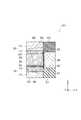
図1は、第1の実施形態に係る半導体装置を例示する模式的断面図である。
図1に表したように、本実施形態に係る半導体装置101は、第1半導体層10と、第2半導体層20と、第3半導体層30と、第1電極40と、を含む。半導体装置101は、さらに、第4半導体層34、絶縁膜43、絶縁層51及び絶縁層52を含む。半導体装置101は、例えば薄膜トランジスタである。(First embodiment)
FIG. 1 is a schematic cross-sectional view illustrating the semiconductor device according to the first embodiment.
As shown in FIG. 1, the
なお、以下の説明において、第1半導体層10から第2半導体層20へ向かう第1方向をZ軸方向とする。Z軸方向に対して垂直な一つの方向をX軸方向とする。X軸方向及びZ軸方向に対して垂直な方向をY軸方向とする。 In the following description, the first direction from the
第1半導体層10は、例えば、第1層11と第2層12とを含む。第2層12は、第1層11の上に積層されており、第1層11と第3半導体層30との間に設けられる。 The
第1半導体層10は、第1導電型の不純物を含む。例えば、第1半導体層10は、第1導電型の不純物として、リン(P)または砒素(As)を含む。第1半導体層10は、第3半導体層30と電気的に接続されている。第1半導体層10は、例えばトランジスタのソース領域及びドレイン領域の一方である。 The
第2層12における第1導電型の不純物の濃度は、第1層11における第1導電型の不純物の濃度よりも低い。例えば、第2層12は、導電性の不純物を実質的に含まない層(例えばノンドープ層)である。第1層11の不純物濃度は、例えば、1×1020cm−3以上1×1023cm−3以下である。第2層12の不純物濃度は、例えば、1×1014cm−3以上1×1020cm−3以下である。The concentration of the first conductivity type impurity in the
なお、この例では、第1導電型がn型であり、第2導電型がp型である。但し、実施形態においては、第1導電型がp型であり、第2導電型がn型であってもよい。p型の不純物としては、例えば、ホウ素(B)やガリウム(Ga)を用いることができる。 In this example, the first conductivity type is n-type, and the second conductivity type is p-type. However, in the embodiment, the first conductivity type may be p-type and the second conductivity type may be n-type. For example, boron (B) or gallium (Ga) can be used as the p-type impurity.
第1層11の厚さ(Z軸方向に沿った長さ)は、例えば、5ナノメートル(nm)以上1マイクロメートル(μm)以下である。第2層12の厚さ(Z軸方向に沿った長さ)は、例えば、1nm以上100nm以下である。 The thickness (length along the Z-axis direction) of the
第1半導体層10(第1層11及び第2層12)は、第1材料の結晶を含む。第1材料には、例えば、シリコン(Si)、ゲルマニウム(Ge)、SixGe1−x(0<x<1)、ガリウムアンチモン(GaSb)、InxGa1−xAs(0≦x≦1)及びInxGa1−xSb(0≦x≦1)の少なくともいずれかを用いることができる。第1半導体層10(第1層11及び第2層12)は、第1材料の多結晶半導体層である。The first semiconductor layer 10 (the
第1半導体層10の第1材料としてSiやGeを用いる場合には、n型の不純物としてPやAsを用いることができ、p型の不純物としてBやGaを用いることができる。第1半導体層10の第1材料として、III-V族化合物(InGaAs、GaAs、GaSb等)を用いる場合には、n型の不純物としてSiを用いることができ、p型の不純物として亜鉛(Zn)やベリリウム(Be)を用いることができる。 When Si or Ge is used as the first material of the
第2半導体層20は、第1方向において第1半導体層10と離間して設けられる。
第2半導体層20は、第3層13と第4層14とを含む。第4層14は、第3層13と第3半導体層30との間に設けられる。The
The
第2半導体層20は、第1導電型の不純物を含む。第2半導体層20は、第3半導体層30と電気的に接続されている。第2半導体層20は、例えばトランジスタのソース領域及びドレイン領域の他方である。 The
第4層14における第1導電型の不純物の濃度は、第3層13における第1導電型の不純物の濃度よりも低い。例えば、第4層14は、導電性の不純物を実質的に含まない層(例えばノンドープ層)である。第3層13の不純物濃度は、例えば、1×1020cm−3以上1×1023cm−3以下である。第4層14の不純物濃度は、例えば、1×1014cm−3以上1×1020cm−3以下である。The concentration of the first conductivity type impurity in the
第3層13の厚さ(Z軸方向に沿った長さ)は、例えば、5ナノメートル(nm)以上1μm以下である。第4層14の厚さ(Z軸方向に沿った長さ)は、例えば、1nm以上100nm以下である。 The thickness (length along the Z-axis direction) of the
第2半導体層20(第3層13及び第4層14)は、第1材料の結晶を含み、例えば、第1材料の多結晶半導体層である。 The second semiconductor layer 20 (the
第3半導体層30は、第1半導体層10と第2半導体層20との間に設けられる。第3半導体層30は、例えばトランジスタのチャネル領域である。第3半導体層30は、第1材料の結晶を含み、例えば、第1材料の多結晶半導体層である。 The
第3半導体層30における第1導電型の不純物濃度は、第1半導体層10における第1導電型の不純物濃度よりも低く、第2半導体層20における第1導電型の不純物濃度よりも低い。例えば、第3半導体層30には、導電性の不純物を実質的に含まない。または、第3半導体層30は、第2導電型の不純物を含んでもよい。これにより、トランジスタの閾値を調整することができる。第3半導体層30には、電気的特性の向上のために、フッ素(F)や水素(H)等の不純物を含んでもよい。第3半導体層30の厚さは、例えば、50nm以上10μm以下である。 The impurity concentration of the first conductivity type in the
第4半導体層34は、第1半導体層10と第3半導体層30との間に設けられる。第4半導体層34は、例えば、第1材料を含む。第4半導体層34は、例えば、第4半導体層34の上に形成される第3半導体層30の結晶性を制御するシード層である。第4半導体層34の厚さは、例えば、1nm以上10nm以下である。 The
第1電極40は、第3半導体層30と対向する。第1電極40の少なくとも一部は、Z軸方向と交差する方向(例えばX軸方向)において、第3半導体層30と並ぶ。第1電極40の少なくとも一部は、Z軸方向と交差する方向において、第3半導体層30と重なる。第1電極40は、例えば、トランジスタのゲート電極である。ゲート長(第1電極40のZ軸方向に沿った長さ)は、例えば、50nm以上10μm以下である。 The
第1電極40は、例えば、タングステン(W)、タンタル(Ta)、窒化タンタル(TaN)、チタン(Ti)、窒化チタン(TiN)、ニッケル(Ni)及びコバルト(Co)の少なくともいずれかを含む。第1電極40は、これらの材料の少なくともいずれかとSiとが反応してできるシリサイド金属を含んでもよい。第1電極40は、不純物を含むポリシリコン(Doped poly-Si)を含んでもよい。 The
絶縁膜43の少なくとも一部は、第3半導体層30と第1電極40との間に設けられる。絶縁膜43は、例えば、トランジスタのゲート絶縁膜である。絶縁膜43には、例えば、酸化シリコン(SiO2)、酸化アルミニウム(Al2O3)、酸化ハフニウム(HfO2)、酸化ジルコニウム(ZrO2)、酸化ランタン(La2O3)、窒化シリコン(SiN)または酸窒化シリコン(SiON)などの材料を用いることができる。絶縁膜43には、これらの材料の積層膜または混合膜を用いてもよい。絶縁膜43の厚さ(X軸方向に沿った長さ)は、例えば、1nm以上100nm以下である。At least a part of the insulating
絶縁層51及び絶縁層52は、Z軸方向において第1電極40と並ぶ。第1電極40は、絶縁層51と絶縁層52との間に設けられる。例えば、絶縁層51は、第1電極40と第1半導体層10との間を絶縁する。絶縁層52は、第1電極40と第2半導体層20との間を絶縁する。なお、絶縁層51は、下部に配線層(配線層61等)が設けられた場合(図3を参照)には、第1電極40と配線層とを絶縁する。また、絶縁層52は、上部に配線層(配線層63等)が設けられた場合(図3を参照)には、第1電極40と配線層とを絶縁する。
絶縁層51には、例えば、酸化シリコン、窒化シリコンまたはポリシラザン(Polysilazane:PSZ)が用いられる。絶縁層52には、例えば、酸化シリコン、窒化シリコンまたはポリシラザンが用いられる。The insulating
For example, silicon oxide, silicon nitride, or polysilazane (PSZ) is used for the insulating
半導体装置101は、例えば、縦型のTFTである。第1〜第3半導体層10〜30は、基板50(図3を参照)の上に設けられ、トランジスタの電流が流れる方向(ソースとドレインとを結ぶチャネル方向)は、基板50の第1面50a(主面)に対して垂直な方向に略平行である。すなわち、第1方向(Z軸方向)は、基板の主面に対して垂直である。実施形態に係る半導体装置は、後述する横型のTFTでもよい。 The
半導体装置101の構造についてさらに説明する。以下の説明においては、第1材料がSiである場合について説明する。すなわち、第1半導体層10、第2半導体層20及び第3半導体層30は、それぞれ、ポリシリコン層である。 The structure of the
第3半導体層30における配向性は、第1半導体層10における配向性よりも高く、第2半導体層20における配向性よりも高い。この場合、例えば、第3半導体層30中の粒界B3の密度は、第1半導体層10中の粒界B1の密度よりも低く、第2半導体層20中の粒界B2の密度よりも低い。例えば、第3半導体層30中の結晶粒G3の大きさの平均は、第1半導体層10中の結晶粒G1の大きさの平均よりも大きく、第2半導体層20中の結晶粒G2の大きさの平均よりも大きい。
例えば、第3半導体層30は、特定の結晶配向性を有する。第1半導体層10及び第2半導体層20は、例えば、特定の結晶配向性を有さない。第1半導体層10及び第2半導体層20においては、例えば結晶がランダムに配向している。The orientation in the
For example, the
すなわち、第3半導体層30におけるSi結晶の特定の方位(第1結晶方位)の配向性は、第1半導体層10におけるSi結晶の当該特定の方位の配向性よりも高い。そして、第3半導体層30における第1結晶方位の配向性は、第2半導体層20における第1結晶方位の配向性よりも高い。つまり、第3半導体層30のうち第1結晶方位に配向した領域の密度は、第1半導体層10のうち第1結晶方位に配向した領域の密度よりも高く、第2半導体層20のうち第1結晶方位に配向した領域の密度よりも高い。
第1結晶方位は、例えば、<100>方向、<110>方向及び<111>方向のいずれかである。That is, the orientation of the specific orientation (first crystal orientation) of the Si crystal in the
The first crystal orientation is, for example, any of the <100> direction, the <110> direction, and the <111> direction.
さらに、第3半導体層30の第1結晶方位の配向性は、第1層11の第1結晶方位の配向性及び第2層12の第1結晶方位の配向性のそれぞれよりも高い。また、第3半導体層30の第1結晶方位の配向性は、第3層13の第1結晶方位の配向性及び第4層14の第1結晶方位の配向性のそれぞれよりも高い。 Furthermore, the first crystal orientation of the
配向性の評価においては、例えば電子線回折法を用いることができる。例えば、半導体装置101の断面構造を取得し、チャネル方向(第1方向)の結晶方位を<100>、<110>及び<111>のいずれかに帰属させる。このとき、第3半導体層30においては、ある特定の1つの方位を向く領域(結晶粒)の割合が、他の2つの方位を向く領域の割合よりも有意に大きい。一方、第1半導体層10及び第2半導体層20においては、特定の結晶方位を向く領域のみが有意に大きな割合を有さない。 In the evaluation of orientation, for example, an electron beam diffraction method can be used. For example, the cross-sectional structure of the
換言すると、第3半導体層30のうち第1方向が第1結晶方位に沿った領域の割合は、第3半導体層30のうち第1方向が第1結晶方位とは異なる結晶方位(第2結晶方位)に沿った領域の割合よりも高い。一方、第1半導体層10のうち第1方向が第1結晶方位に沿った領域の割合は、第1半導体層10のうち第1方向が第2結晶方位に沿った領域の割合と実質的に同じである。また、第2半導体層20のうち第1方向が第1結晶方位に沿った領域の割合は、第2半導体層20のうち第1方向が第2結晶方位に沿った領域の割合と実質的に同じである。 In other words, the proportion of the
なお、ここで「割合」とは、観察した断面において、評価対象の半導体層の面積に対する、着目している結晶方位に配向した領域の面積の比率である。または、「割合」は、評価対象の半導体層の体積に対する、着目している結晶方位に配向した領域の体積の比率であってもよい。 Here, “ratio” is the ratio of the area of the region oriented in the crystal orientation of interest to the area of the semiconductor layer to be evaluated in the observed cross section. Alternatively, the “ratio” may be the ratio of the volume of the region oriented in the crystal orientation of interest to the volume of the semiconductor layer to be evaluated.
例えば、ゲート長が短い場合、第3半導体層30において、Z軸方向に沿って延在する粒界は、X軸方向またはY軸方向に沿って延在する粒界よりも多い。一方、第1及び第2半導体層中において、Z軸方向に沿って延在する粒界が生じる頻度は、X軸方向またはY軸方向に沿って延在する粒界が生じる頻度と実質的に等しい。 For example, when the gate length is short, in the
図1に表したように、第1電極40は、第1端部E1と第2端部E2とを有する。第1端部及び第2端部E2は、第1方向において互いに離間した端部である。
第1端部E1は、第1方向と交差する方向(例えばX軸方向)において、第3半導体層30及び第2層12のいずれかと重なる。この例では、第1端部E1は、X軸方向において第2層12と重なっている。第1端部E1は、X軸方向において第1層11とは重ならない。As shown in FIG. 1, the
The first end E1 overlaps with either the
第2端部E2は、第1方向と交差する方向において、第3半導体層30及び第4層14のいずれかと重なる。この例では、第2端部E2は、X軸方向において第4層14と重なっている。第2端部E2は、X軸方向において第3層13とは重ならない。 The second end E2 overlaps with either the
ところで、チャネル材料にポリシリコンが用いられたトランジスタにおいて、チャネル中には、例えば、数多くの粒界が存在する。このため、チャネル材料にポリシリコンを用いたトランジスタにおいては、単結晶Siを用いたトランジスタと比べて、キャリアが粒界ポテンシャルの影響を受けやすい。これにより、キャリア移動度の低下、S値(サブスレッショルドスロープ)の低下及び閾値のシフトなどが生じやすい。
これに対して、チャネル中を垂直に粒界が横切らないような結晶粒の配向制御によって、キャリアの移動度の低下などを抑制することができる。前述したように、実施形態に係る半導体装置101においては、第3半導体層30における第1結晶方位の配向性は、第1半導体層10における第1結晶方位の配向性よりも高い。例えば、半導体装置101のチャネルにおいては、電流が流れる方向と平行となるように結晶配向が揃っている。これにより、キャリアがソースからドレインへ移動する際に、粒界を横切る確率が低下する。したがって、粒界ポテンシャルのキャリアへの影響が低減され、移動度を向上させることができる。閾値のシフトやS値の低下を抑制することができ、良好なサブスレッショルド特性を得ることができる。By the way, in a transistor in which polysilicon is used as a channel material, for example, many grain boundaries exist in the channel. Therefore, in a transistor using polysilicon as a channel material, carriers are more susceptible to the grain boundary potential than a transistor using single crystal Si. This tends to cause a decrease in carrier mobility, a decrease in S value (subthreshold slope), a shift in threshold value, and the like.
In contrast, a decrease in carrier mobility and the like can be suppressed by controlling the crystal grain orientation so that the grain boundaries do not cross vertically in the channel. As described above, in the
さらに、実施形態においては、前述したように、第1電極40の第1端部E1が不純物濃度の低い第2層12と重なり、第2端部E2が不純物濃度の低い第4層14と重なっている。第1電極40は、X軸方向において、不純物濃度の高い第1層11及び第3層13とは重ならない。これにより、GIDL(Gate Induced Drain Leakage)などによるリーク電流を低減することができる。また、第1電極40の端部が第2層12及び第4層14とオーバーラップすることにより、寄生抵抗の増大が抑制される。 Furthermore, in the embodiment, as described above, the first end E1 of the
そして、第1半導体層10及び第2半導体層20においては結晶粒の配向性が低いため、ソース・ドレイン領域からの不純物拡散が抑制される。例えば、粒界に沿って不純物がチャネルへ熱拡散することが抑制される。これにより、さらにGIDLを抑制することができる。 In the
以上説明したように、実施形態では、チャネルを形成するポリシリコン層の結晶粒は、特定方向の配向性を有する。このため、例えば、チャネルを垂直方向に横切る粒界が減少する。これにより、チャネル中に生じていた粒界ポテンシャルの影響が低減され、閾値増大や移動度低下などのトランジスタ特性の劣化を抑制できる。また、ソース・ドレイン領域近傍の結晶のみ配向性を持たせないことで、ソース・ドレイン間に生じるオフリークを低減することを可能とする。 As described above, in the embodiment, the crystal grains of the polysilicon layer forming the channel have orientation in a specific direction. For this reason, for example, the grain boundaries crossing the channel in the vertical direction are reduced. Thereby, the influence of the grain boundary potential generated in the channel is reduced, and deterioration of transistor characteristics such as an increase in threshold and a decrease in mobility can be suppressed. In addition, since only the crystal in the vicinity of the source / drain region is not oriented, off-leakage generated between the source / drain can be reduced.
図2(a)及び図2(b)は、第1の実施形態に係る別の半導体装置を例示する模式的断面図である。
図2(a)に表した半導体装置101aにおいては、第1電極40の第1端部E1は、X軸方向において、第2層12と第4半導体層34との境界と重なっている。第2端部E2は、X軸方向において第4層14と第3半導体層30との境界と重なっている。すなわち、第1電極40の端部は、結晶がランダムに配向した領域と特定の配向性を有する領域との境界と重なっている。
図2(b)に表した半導体装置101bにおいては、第1端部E1及び第2端部E2は、それぞれ、X軸方向において第3半導体層30と重なっている。
上記以外については、半導体装置101a及び101bには、図1に関して説明した半導体装置101と同様の説明を適用することができる。FIG. 2A and FIG. 2B are schematic cross-sectional views illustrating another semiconductor device according to the first embodiment.
In the
In the
Except for the above, the description similar to the
半導体装置101a及び101bにおいても、図1の半導体装置101と同様に、チャネルを形成する第3半導体層30の結晶粒は、特定方向の配向性を有する。これにより、チャネル中の粒界ポテンシャルの影響が低減され、閾値の増大やキャリアの移動度の低下などのトランジスタ特性の劣化を抑制することができる。 Also in the
さらに、第1半導体層10及び第2半導体層20における結晶の配向性が低いため、不純物がチャネル領域へ拡散しにくい。そして、第1電極40は、不純物濃度の高い第1層11及び第3層13と重ならないため、リーク電流を抑制することができる。半導体装置101a及び101bにおいては、第1電極40と第1及び第2半導体層とのオーバーラップ量が、半導体装置101に比べて小さいため、さらにリーク電流を抑制することができる。 Furthermore, since the crystal orientation in the
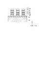
図3は、第1の実施形態に係るさらに別の半導体装置を例示する模式的断面図である。図3に表した半導体装置102は、複数のトランジスタ(半導体装置101c)を含む。 さらに、半導体装置102は、基板50と、絶縁層60と、配線層61と、コンタクト層62と、保護膜53と、コンタクト層64と、配線層63と、を含む。 FIG. 3 is a schematic cross-sectional view illustrating still another semiconductor device according to the first embodiment. The
複数の半導体装置101cは、X−Y平面においてアレイ状に並べられて設けられる。例えば、複数の半導体装置101cの上に図示しないデバイスが積層される。積層されるデバイスは、例えばメモリセルアレイであり、この場合、複数の半導体装置101cは、メモリのドライバトランジスタとして機能する。
なお、メモリセルアレイは、複数の半導体装置101cの下側に配置されてもよい。例えば、基板50と絶縁膜60との間にメモリセルアレイが配置されてもよい。また、基板50には、CMOS等の回路が形成されていてもよい。The plurality of
Note that the memory cell array may be disposed below the plurality of
図3に表した例では、1つの第3半導体層30は、2つの第1電極40の間に設けられている。すなわち、このトランジスタは、ダブルゲート構造を有する。半導体装置101cにおいては、絶縁膜43の一部は、第1電極40と絶縁層51との間、及び、第2半導体層20と絶縁層52との間、にも設けられている。
これ以外については、半導体装置101cには、図1に関して説明した半導体装置101と同様の説明を適用することができる。例えば、複数の第3半導体層30における第1結晶方位の配向性は、複数の第1半導体層10における第1結晶方位の配向性よりも高い。また、複数の第3半導体層30のうちチャネル方向が第1結晶方位に沿った領域の割合は、複数の第3半導体層30のうちチャネル方向が第1結晶方位とは異なる方位に沿った領域の割合よりも高い。In the example shown in FIG. 3, one
Except for this, the same description as the
なお、半導体装置101cの替わりに、前述した半導体装置101aまたは101b等を用いてもよい。また、複数のトランジスタ(半導体装置101c)は、シングルゲート構造であってもよい。 Note that the
基板50は、例えば、支持基板であり、Si基板を用いることができる。
絶縁層60は、基板50の上に設けられ、複数の半導体装置101cと基板50との間に配置されている。絶縁層60は、酸化シリコン(SiO2)、窒化シリコン(SiN)または酸化アルミニウム(Al2O3)を含む。The
The insulating
絶縁層60は、例えば、基板50を酸化することで得られる熱酸化膜である。または、絶縁層60は、スパッタ装置やCVD(Chemical Vapor Deposition)装置等によって堆積された絶縁膜である。絶縁層60には、これらの熱酸化膜及び絶縁膜を組み合わせた積層膜を用いてもよい。絶縁層60によって、基板50と配線層61との絶縁性が保たれる。 The insulating
配線層61及びコンタクト層62は、複数の半導体装置101cと絶縁層60との間に設けられる。配線層61及びコンタクト層62は、第1半導体層10と電気的に接続されている。 The
配線層61及びコンタクト層62には、500℃以上の温度に対する耐熱性を有する金属材料を用いることが好ましい。例えば、配線層61には、WやTiを含む金属材料を用いることができる。コンタクト層62には、W、Ti、TiN、Ni、Co、白金(Pt)及びパラジウム(Pd)の少なくともいずれかを用いることができる。 For the
保護膜53は、コンタクト層62と絶縁層51との間、及び、第1半導体層10と絶縁層51との間に設けられる。保護膜53は、例えばSiNを含む。 The
複数の半導体装置101cは、配線層63と配線層61との間に設けられる。コンタクト層64は、配線層63と第2半導体層20との間に設けられる。配線層63及びコンタクト層64は、第2半導体層20と電気的に接続されている。 The plurality of
コンタクト層64は、ポリシリコン層(第2半導体層20)とコンタクトする。このため、コンタクト層64には、コンタクト抵抗の低い金属材料として、コンタクト層62と同様に、W、Ti、TiN、Ni、Co、Pt、Pd等を含む金属材料を用いることができる。 The
配線層63に用いられる材料は、例えば、半導体装置101cの上に積層されるデバイスの熱負荷によって決められる。500℃以上の熱負荷が掛かる場合には、配線層63には、配線層61と同様に、WやTiを含む金属材料を用いることができる。熱負荷が500℃未満の場合には、配線層63には、AlやCu等の耐熱性が低いものの低抵抗な金属材料を用いることができる。 The material used for the
半導体装置102においても、ポリシリコン層(第1半導体層10及び第2半導体層20)と第1電極40とがオーバーラップする領域において、ポリシリコンは、特定の配向性を有していない。さらに、ゲート直下のチャネル領域(第3半導体層30)において、ポリシリコンは配向性を有する。これにより、キャリアの高移動度と、低リークと、を両立したTFTを実現することが可能となる。 Also in the
半導体装置102の配向性の評価においても、例えば電子線回折法を用いることができる。一例として示すと、まず、複数の(縦型または横型)TFTのチャネル中央部を含む断面、複数のTFTのチャネル端部を含む断面、または、複数のTFTのソース(またはドレイン)領域を含む断面、を取得する。各断面は、例えば、X−Y平面に対して平行である。そして、各断面(各観測点)において、ポリシリコンの結晶の配向方向を電子線回折法によって確認する。典型的な結晶の配向方向は、例えば、<100>方向、<110>方向及び<111>方向である。このとき、<100>方向±10°以内に配向している結晶粒、<110>方向±10°以内に配向している結晶粒、及び、<111>方向±10°以内に配向している結晶粒、をそれぞれ抽出する。そして、それぞれの方位について、当該方位に配向している結晶粒の割合を見積もる。ここで、「割合」は、観察した断面において、複数の半導体層全体の面積に対する、着目した方位に配向している結晶粒の面積の割合である。または、「割合」は、複数の半導体層全体の体積に対する、着目した方位に配向している結晶粒の体積の割合であってもよい。 In the evaluation of the orientation of the
この割合のうち、ある特定の方位を向く結晶の割合が、他の方位を向く結晶の割合よりも有意に高い場合、当該断面(当該観測点)においてポリシリコン層が当該特定の方位に配向していると定義する。例えば、<111>方向を向く結晶の割合が、他の方位を向く結晶の割合よりも有意に高い場合(例えば、<111>方向を向く結晶の割合が全体の50%以上を占める場合等)、当該断面においてポリシリコン層が<111>配向している、とすることができる。 When the proportion of crystals facing a specific orientation is significantly higher than the proportion of crystals facing other orientations, the polysilicon layer is oriented in the particular orientation in the section (the observation point). It is defined that For example, when the proportion of crystals facing the <111> direction is significantly higher than the proportion of crystals facing the other orientation (for example, when the proportion of crystals facing the <111> direction accounts for 50% or more of the total) In the cross section, the polysilicon layer may be <111> oriented.
例えば、第1〜第3半導体層の幅が狭い場合においても、上記のようにして配向性を評価することができる。すなわち、セルサイズが微細な場合においても、複数のトランジスタに亘って統計をとることで配向性を評価することができる。 For example, even when the widths of the first to third semiconductor layers are narrow, the orientation can be evaluated as described above. That is, even when the cell size is fine, the orientation can be evaluated by taking statistics over a plurality of transistors.
なお、本構造の観測に用いられる手法は、上記のみに限定されるものではない。また結晶の配向方向は、上述した3方位のみに限られるものではない。 Note that the method used for observation of this structure is not limited to the above. Further, the orientation direction of the crystal is not limited to the above three orientations.
次に半導体装置102の製造方法について説明する。
図4(a)〜図4(c)は、実施形態に係る半導体装置の製造方法を例示する工程順模式的断面図である。Next, a method for manufacturing the
FIG. 4A to FIG. 4C are schematic cross-sectional views in order of the processes, illustrating the method for manufacturing a semiconductor device according to the embodiment.
図4(a)に表したように、基板50の上に、絶縁層60、配線層61及びコンタクト層62をこの順に積層する。前述したように、絶縁層60の形成には、基板50の酸化、または、スパッタ装置やCVD装置等による堆積、を用いることができる。 As illustrated in FIG. 4A, the insulating
コンタクト層62の上に、第1半導体層10(第1層11及び第2層12)として多結晶半導体層を形成する。第1半導体層10の形成においては、結晶粒の結晶方位に配向性が生じないような条件で多結晶半導体層を形成する。例えば、LPCVD装置等を用いて、コンタクト層62の上に直接ポリシリコン層を形成することで、多結晶半導体層を形成することができる。または、500℃以上の温度にてSiH4ガスを用いてCVD装置等でアモルファスシリコン層を形成した後、アモルファスシリコン層を結晶化させることで多結晶半導体層を形成してもよい。ポリシリコン層を形成した後にSi等のイオン注入によってポリシリコン層の非晶質化を行ってから、再結晶化を行ってもよい。A polycrystalline semiconductor layer is formed on the
第1層11が含有する第1導電型の不純物の導入には、イオン注入が用いられる。または、CVD装置内におけるin−situプロセスによって、第1層11の形成時に不純物を導入してもよい。第1層11のシート抵抗の低減、及び、チャネルや配線層とのコンタクト抵抗の低減のため、第1層11における第1導電型の不純物濃度は、1×1020cm−3以上であることが好ましい。前述したように、第2層12には、例えば、導電性を付与する不純物を導入しない。Ion implantation is used to introduce the first conductivity type impurities contained in the
導電性を付与する不純物以外に、ポリシリコンの電気的特性の向上のためのFやH、歪導入のための炭素(C)やGe、配線層とのシリサイド化抑制のための窒素(N)などを第1半導体層10に導入してもよい。 In addition to impurities that impart conductivity, F and H for improving the electrical characteristics of polysilicon, carbon (C) and Ge for introducing strain, and nitrogen (N) for suppressing silicidation with the wiring layer Or the like may be introduced into the
図4(b)に表したように、第1半導体層10の上に第4半導体層34となるシード層34fを形成する。シード層34fは、非晶質であるアモルファスシリコン層を低温で形成することで得られる。例えば、シード層34fは、CVD装置にてSi2H6ガスを用いて450℃未満の低温で形成される。ここで形成される層の厚さは、例えば5nm以下である。As shown in FIG. 4B, a
シード層34fの上に、第3半導体層30(チャネル)となるアモルファスシリコン層30fを形成する。アモルファスシリコン層30fは、第4半導体層34に比べて高い温度で形成されることが好ましい。例えば、CVD装置にてSiH4ガスを用いて500℃以上の温度で、アモルファスシリコン層30fを形成することができる。An
その後、チャネルを結晶化させるため、650℃以下の熱処理を加える。これにより、アモルファスシリコン層30f及びシード層34fをポリシリコン層へと結晶化させて、第3半導体層30及び第4半導体層34を形成する。 Thereafter, heat treatment at 650 ° C. or lower is applied to crystallize the channel. As a result, the
Si2H6ガスを用いて低温で形成されたシード層34fが存在することで、シード層34fからの核発生が減少するとともに歪みが増加する。これにより、例えば、基板垂直方向に<111>配向したポリシリコン層(第3半導体層30)が得られる。このため、チャネル方向に対して交差する方向(例えば垂直な方向)にチャネルを横切る結晶粒界が減少する。The presence of the
その後、図4(c)に表したように、第3半導体層30の上に、導電性を付与する不純物を含まない第4層14を形成する。さらに、第4層14の上に、第1導電型の不純物を含む第3層13を形成して、第2半導体層20を形成する。 Thereafter, as illustrated in FIG. 4C, the
第2半導体層20は、第1半導体層10と同様に、ポリシリコン中の結晶粒に配向性が生じないように形成される。このためには、ポリシリコンをLPCVD法によって直接、第3半導体層30の上に堆積する。または、ポリシリコン層を形成した後にSiやGe等のイオン注入によってポリシリコン層の非晶質化を行ってから、再結晶化を行ってもよい。 Similar to the
図5(a)〜図5(c)は、第1の実施形態に係る半導体装置の製造方法を例示する工程順模式的断面図である。
これらの図は、図4(c)に続く、半導体装置102の製造工程を例示している。図5(a)に表したように、反応性イオンエッチング(Reactive Ion Etching:RIE)プロセスにて、第1〜第4半導体層をエッチングする。これにより、複数の柱状の縦型FET構造80を形成する。FIG. 5A to FIG. 5C are schematic cross-sectional views in order of the processes, illustrating the method for manufacturing the semiconductor device according to the first embodiment.
These drawings illustrate the manufacturing process of the
図5(b)に表したように、第1〜第3半導体層及びコンタクト層62を覆うように保護膜53としてSiN膜を形成する。保護膜53の形成には、例えば、原子層堆積(Atomic Layer deposition:ALD)プロセスを用いることができる。 As shown in FIG. 5B, a SiN film is formed as the
その後、保護膜53の上にgap−fill膜としてALD−SiO2またはポリシラザンを堆積する。そして、RIEプロセス等によって、gap−fill膜をエッチバックする。これにより、第1半導体層10同士の間に埋め込まれた絶縁層51が形成される。Thereafter, ALD-SiO2 or polysilazane is deposited on the
その後、図5(c)に表したように、第2層12の一部が露出するように、ウェット処理等によって、保護膜53をエッチバックする。このエッチバックプロセスによって、第1電極40とソース領域(第1半導体層10)とのオーバーラップ量が決まる。このため、図3に示した半導体装置101cの場合には、第2層12の一部のみが露出するように、エッチングが行われる。なお、エッチング量を調整することで、図2(a)及び図2(b)に示したような第1電極40を形成することも可能である。 Thereafter, as shown in FIG. 5C, the
図6(a)及び図6(b)は、第1の実施形態に係る半導体装置の製造方法を例示する工程順模式的断面図である。
これらの図は、図5(c)に続く、半導体装置102の製造工程を例示している。図6(a)に表したように、絶縁膜43を第1〜第3半導体層及び絶縁層51の上に、ALDプロセスまたはCVDプロセスによって形成する。FIGS. 6A and 6B are schematic cross-sectional views in order of the processes, illustrating the method for manufacturing the semiconductor device according to the first embodiment.
These drawings illustrate the manufacturing process of the
その後、絶縁膜43の上に、第1電極40となる導電層をALDまたはCVDによって堆積する。この導電層をRIEプロセス等によってエッチバックすることで、第1電極40が形成される。このとき、第4層14の一部のみが第1電極40とX軸方向においてオーバーラップするようにエッチングが行われる。これにより、前述したように、GIDL等のリーク電流を抑制することができる。 Thereafter, a conductive layer to be the
その後、第1電極40及び絶縁膜43の上に、ALDプロセスやCVDプロセスによって、絶縁層52を形成する。図6(b)に表したように、絶縁層52は、化学機械研磨(Chemical Mechanical Polishing:CMP)プロセスにて平坦化される。このとき、第2半導体層20上の絶縁膜43の一部も除去される。第2半導体層20上の絶縁膜43の一部は、ウェット処理等によって除去されても良い。 Thereafter, the insulating
その後、第2半導体層20上にコンタクト層64及び配線層63を堆積する。これにより、図3に表した半導体装置102が形成される。 Thereafter, a
なお、図5(a)においては、第1半導体層10の下部に設けられた配線層61及びコンタクト層62が共通化されている。但し、実施形態においては、図7のように、配線層61及びコンタクト層62が複数の配線に分断されていてもよい。複数の第1半導体層10のそれぞれは、互いに異なる配線に接続されている。 In FIG. 5A, the
配線層63の形成後には、さらに、配線層63上にデバイスを形成すればよい。例えば、配線層63の上に再度、多結晶半導体TFTを形成することも可能である。3次元積層メモリとして、金属と酸化物とを用いたReRAM等を積層してもよい。または、配線層63上に層間絶縁膜を形成した後に、基板貼り合わせ技術を用いて、バルクSi−CMOSやIII−V族化合物半導体のチップを貼り合わせて新たな回路を実現することも可能である。 After the formation of the
以上説明した半導体装置102においては、トランジスタ(半導体装置101c)は、反転型の電界効果トランジスタである。但し、実施形態において、トランジスタは、蓄積型の電界効果トランジスタであってもよい。 In the
蓄積型トランジスタの形成方法は、シード層34fを形成するまでは、上述の方法と同様である。蓄積型トランジスタの形成においては、チャネルとなるアモルファスシリコン層30fを形成する際、第1層11に含まれる不純物と同じ導電型の不純物をアモルファスシリコン層30fに導入する。すなわち、第1層11にPやAsが導入されていた場合、アモルファスシリコン層30fにもPやAsを導入する。
例えば、アモルファスシリコン層30f中の不純物濃度は、1×1018cm−3以上である。ここで、チャネル中の不純物濃度は、ソース・ドレイン領域と同程度(例えば1×1020cm−3以上)でもよいが、チャネル厚(チャネル長)によってはカットオフ特性が劣化する。このため、チャネル幅が10nm以下でない場合は、濃度を低めに設定することが好ましい。蓄積型のトランジスタにおいても、チャネル中の欠陥を終端するためにFやH等の不純物を導入してもよい。この後、結晶化アニールとして650℃以下の熱処理を行うことで、シード層34fとアモルファスシリコン層30fとを結晶化する。これにより、第3半導体層30及び第4半導体層34としてポリシリコン層を形成する。The method for forming the storage transistor is the same as that described above until the
For example, the impurity concentration in the
蓄積型トランジスタにおいては、反転型トランジスタとは異なり、チャネルとソースの導電型が同じである。このため、蓄積型トランジスタにおいては、反転型トランジスタに比べて、チャネルへの不純物拡散による閾値変調が低減される。したがって、蓄積型トランジスタは、閾値の調整において有効である。一方で、先述したように、チャネル中の不純物濃度にもよるが、蓄積型トランジスタのチャネル厚が10nm程度以下の薄膜でない場合には、サブスレッショルド特性が劣化してしまうことがある。
結晶化により第3半導体層30を形成した後には、ドレイン領域を形成し、ポリシリコン層をピラー形状に加工する。以降の工程は、反転型トランジスタの形成と同様であるため省略する。In the storage transistor, unlike the inverting transistor, the conductivity type of the channel and the source is the same. For this reason, in the storage transistor, threshold modulation due to impurity diffusion into the channel is reduced as compared with the inversion transistor. Therefore, the storage transistor is effective in adjusting the threshold value. On the other hand, as described above, depending on the impurity concentration in the channel, if the channel thickness of the storage transistor is not a thin film of about 10 nm or less, the subthreshold characteristics may be deteriorated.
After the
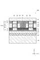
図8は、第1の実施形態に係るさらに別の半導体装置を例示する模式的断面図である。 実施形態に係る半導体装置は、図3に表した半導体装置102の例に限られず、例えば、図8に表した半導体装置104のようであってもよい。 FIG. 8 is a schematic cross-sectional view illustrating still another semiconductor device according to the first embodiment. The semiconductor device according to the embodiment is not limited to the example of the
半導体装置104は、図3に関して説明した半導体装置102と同様に、複数のトランジスタ(半導体装置101d)、基板50、絶縁層60、配線層61、コンタクト層62、保護層53、コンタクト層64及び配線層63を含む。 Similar to the
図8の例では、複数の第3半導体層30のうち互いに隣合う第3半導体層30同士の間に、2つの第1電極40が設けられる。絶縁層52の一部は、上記の2つの第1電極40同士の間にも設けられる。これ以外については、半導体装置104には、図3に関して説明した半導体装置102と同様の説明を適用することができる。 In the example of FIG. 8, two
(第2の実施形態)
図9は、第2の実施形態に係る半導体装置を例示する模式的断面図である。
図9に示した半導体装置103においても、第1半導体層10、第2半導体層20、第3半導体層30、第4半導体層34、第1電極40、絶縁膜43、が設けられる。これらについては、図1の半導体装置101における説明と、同様の説明を適用することができる。半導体装置103は、さらに、基板70、絶縁層71、絶縁層72、絶縁層73、絶縁層75及び第5半導体層35を含む。(Second Embodiment)
FIG. 9 is a schematic cross-sectional view illustrating a semiconductor device according to the second embodiment.
Also in the
基板70は、例えば、支持基板である。支持基板には、Si基板を用いることができる。図9に表したように基板70は、第1面70a(主面)を有する。 The
本実施形態に係る半導体装置103は、例えば、横型のトランジスタである。すなわち、第1〜第3半導体層等は、第1面70aの上に設けられ、ソースとドレインとを結ぶチャネル方向は、第1面70aに対して平行である。 The
絶縁層71は、基板70の第1面70a上に設けられる。絶縁層71の材料には、例えば、SiN、Al2O3またはSiO2等が用いられる。The insulating
絶縁層72及び絶縁層73は、絶縁層71の一部71aと別の一部71bとの間において、絶縁層71(71c)の上に設けられる。絶縁層72及び絶縁層73は、例えば、Al2O3またはSiO2等を含む。The insulating
第1半導体層10は、絶縁層72と絶縁層73との間に位置し、第3半導体層30は、第1半導体層10と絶縁層73との間に位置し、第2半導体層20は、第3半導体層30と絶縁層73との間に位置する。 The
第5半導体層35は、第2半導体層20と第3半導体層30との間に設けられる。なお、第5半導体層35の材料等は、第4半導体層34と同様である。 The
絶縁層75は、例えば、第1電極40の側面の一部を覆うように設けられる。絶縁層75は、例えば、ゲート電極の側壁である。絶縁層75の材料として、SiO2やSiNを用いることができる。The insulating
次に半導体装置103の製造方法について説明する。
図10(a)〜図10(d)は、第2の実施形態に係る半導体装置の製造方法を例示する工程順模式的断面図である。
図10(a)に表したように、基板70の上に絶縁層71を形成する。絶縁層71の形成においては、まず基板70上に絶縁膜を形成し、リソグラフィ及びRIEプロセスによって、この絶縁膜をパターニングする。これにより、絶縁層71には凹部71eが形成される。多結晶半導体層(第1〜第3半導体層)を含むTFT構造は、この凹部71eに埋め込まれる。Next, a method for manufacturing the
FIG. 10A to FIG. 10D are schematic cross-sectional views in order of the processes, illustrating the method for manufacturing a semiconductor device according to the second embodiment.
As shown in FIG. 10A, the insulating
多結晶半導体層としてポリシリコンを用いる場合には、絶縁層71の材料として、絶縁層71上にアモルファスシリコン膜を形成することが困難となる材料が用いられる。例えば、SiNやAl2O3を用いることができる。一方、多結晶半導体層としてIII−V族化合物を用いる場合には、絶縁層71の材料には、SiO2やSiN等が用いられる。When polysilicon is used as the polycrystalline semiconductor layer, a material that makes it difficult to form an amorphous silicon film on the insulating
その後、図10(b)に表したように、例えばALDプロセス等によって、絶縁層71上に絶縁膜を形成した後、RIE等によって凹部71eの側面のみに絶縁膜を形成する。これにより、絶縁層72及び絶縁層73が形成される。 Thereafter, as shown in FIG. 10B, after an insulating film is formed on the insulating
多結晶半導体層にInGaAsやGaSb等のIII−V族化合物半導体が用いられる場合には、絶縁層72及び絶縁層73としてAl2O3膜等を用いることができる。多結晶半導体層にSiやGe等のIV族の材料が用いられる場合には、絶縁層72及び絶縁層73としてSiO2膜等を用いることができる。When a III-V group compound semiconductor such as InGaAs or GaSb is used for the polycrystalline semiconductor layer, an Al2 O3 film or the like can be used as the insulating
なお、以下の例では、多結晶半導体層の材料としてポリシリコンを用い、絶縁層72及び絶縁層73の材料としてSiO2を用いた場合について述べる。但し、実施形態における多結晶半導体層の材料は、上記に限定されない。例えば、多結晶半導体層の材料として、Si、Ge、SixGe1−x(0<x<1)、GaSb、InAsまたはInxGa1−xAs(0<x<1)を用いてもよい。In the following example, a case where polysilicon is used as the material of the polycrystalline semiconductor layer and SiO2 is used as the material of the insulating
その後、図10(c)に表したように、第1半導体層10及び第2半導体層20を形成する。第1半導体層10及び第2半導体層20は、第1の実施形態と同様に、結晶粒が特定の配向性を有さないように形成される。そのためには、例えば、LPCVD等によって、絶縁層71上に直接ポリシリコン層を形成する。または、500℃以上の温度においてSiH4ガスを用いてアモルファスシリコン層を形成した後、600℃以上の熱処理によって結晶化を行う。このアモルファスシリコン層の形成に用いられる条件においては、絶縁層72、73上にアモルファスシリコンが形成され、絶縁層71上にはアモルファスシリコンが形成されにくい。Thereafter, as shown in FIG. 10C, the
その後、第4半導体層34及び第5半導体層35となるアモルファスシリコン層(シード層)を形成する。例えば、CVD装置によってSi2H6ガスを用いて450℃未満の低温において、シード層を形成することができる。シード層の厚さ(チャネル方向に沿った長さ)は、例えば5nm以下である。シード層を形成することによって、第3半導体層30の結晶性を制御することができる。Thereafter, an amorphous silicon layer (seed layer) to be the
シード層を形成した後に、第3半導体層30となるアモルファスシリコン層をさらに形成する。例えば、このアモルファスシリコン層は、CVD装置によって、SiH4ガスを用いて500℃以上の温度において形成される。形成されたアモルファスシリコン層には、閾値調整のために導電性を付与する不純物を導入することができる。例えば、pMOSFETを形成する場合には、不純物としてPやAsが用いられ、nMOSFETを形成する場合には、不純物としてBやBF2を用いることができる。電気的特性の向上のために、FやHが導入されてもよい。After forming the seed layer, an amorphous silicon layer to be the
その後、600℃以上の熱処理を行う。これにより、アモルファスシリコンをポリシリコンへと結晶化させる。結晶化後においては、第3半導体層30、第4半導体層34及び第5半導体層35のみが第1面70aと平行な方向への結晶粒の配向性を持つ。第1半導体層10及び第2半導体層20においては、結晶粒の配向性は低い(例えば配向性はない)。 Thereafter, heat treatment at 600 ° C. or higher is performed. Thereby, amorphous silicon is crystallized into polysilicon. After crystallization, only the
凹部71eよりも上部へ突出したSiを除去するためCMPプロセスによって平坦化する。これにより、中央部のポリシリコン層のみが結晶配向性を有する平坦なポリシリコン層を得ることができる。なお、チャネル中への不純物導入は、CMPによる平坦化を行った後に行われてもよく、さらに再結晶化アニールが行われてもよい。 Planarization is performed by a CMP process to remove Si protruding upward from the
チャネルであるポリシリコン層を形成した後の製造工程は、通常のTFT形成プロセスフローと同様である。
図10(d)に表したように、例えば、少なくとも第3半導体層30の上に、絶縁膜43及び第1電極40を積層して、ゲートスタック構造を形成する。ゲートスタック構造の形成には、リソグラフィ及びRIEプロセスを用いることができる。The manufacturing process after forming the polysilicon layer as the channel is the same as the normal TFT formation process flow.
As illustrated in FIG. 10D, for example, the insulating
ゲートスタック構造を形成した後に、絶縁層75となるSiO2膜等を、第1電極40の側面及び上面を覆うように積層する。その後、RIEプロセスによって側壁として絶縁層75を形成する。After forming the gate stack structure, an SiO2 film or the like that becomes the insulating
その後、ソース・ドレイン領域(第1半導体層10の一部及び第2半導体層20の一部)に、不純物のイオン注入を行う。nMOSFETを形成する場合には、不純物としてPやAsを注入する。pMOSFETを形成する場合には、不純物としてBやBF2を注入する。さらに、歪みを導入するためにnMOSFETの場合には、不純物としてCを導入してもよく、pMOSFETの場合にはGeを導入してもよい。イオン注入の後に、活性化アニールを行う。その後、Ni等の金属材料を用いて、セルフアラインプロセスによって、ソース・ドレイン領域に、シリサイド層を形成する。そして、シリサイド層と電気的に接続された配線層を適宜形成する。Thereafter, impurity ions are implanted into the source / drain regions (a part of the
以上説明したようにして、図9に表した半導体装置103を形成することができる。
横型のTFTである半導体装置103においても、縦型のTFTである半導体装置101と同様に、チャネル中のみ結晶粒の配向性が高い。このため、閾値のシフトやキャリアの移動度低下などのトランジスタ特性の劣化を抑制することができる。
横型のTFTにおいては、側壁の形成後にソース・ドレイン領域の不純物注入が行われる。このため、チャネル方向に対して垂直な方向において、第1電極40は、不純物濃度の高いソース・ドレイン領域と重ならない。これにより、GIDLを抑制することができ、リーク電流を低減することができる。さらに、第1の実施形態と同様に、第1電極の端部の直下には、配向性の低い第1半導体層10及び第2半導体層20が位置する。このため、ソース・ドレイン領域からチャネルへの不純物の拡散が抑制される。したがって、この点からもGIDLが抑制され、リーク電流を低減することができる。As described above, the
Also in the
In the lateral TFT, the impurity implantation of the source / drain regions is performed after the sidewalls are formed. For this reason, in the direction perpendicular to the channel direction, the
実施形態によれば、キャリアの移動度を向上させた半導体装置が提供できる。 According to the embodiment, a semiconductor device with improved carrier mobility can be provided.
なお、本願明細書において、「垂直」及び「平行」は、厳密な垂直及び厳密な平行だけではなく、例えば製造工程におけるばらつきなどを含むものであり、実質的に垂直及び実質的に平行であれば良い。「電気的に接続」には、直接接触して接続される場合の他に、他の導電性部材などを介して接続される場合も含む。 In the present specification, “vertical” and “parallel” include not only strictly vertical and strictly parallel, but also include, for example, variations in the manufacturing process, and may be substantially vertical and substantially parallel. It ’s fine. “Electrically connected” includes not only the case of being connected in direct contact but also the case of being connected via another conductive member.
以上、具体例を参照しつつ、本発明の実施の形態について説明した。しかし、本発明の実施形態は、これらの具体例に限定されるものではない。例えば、第1半導体層、第2半導体層、第3半導体層及び第1電極などの各要素の具体的な構成に関しては、当業者が公知の範囲から適宜選択することにより本発明を同様に実施し、同様の効果を得ることができる限り、本発明の範囲に包含される。
また、各具体例のいずれか2つ以上の要素を技術的に可能な範囲で組み合わせたものも、本発明の要旨を包含する限り本発明の範囲に含まれる。The embodiments of the present invention have been described above with reference to specific examples. However, embodiments of the present invention are not limited to these specific examples. For example, regarding the specific configuration of each element such as the first semiconductor layer, the second semiconductor layer, the third semiconductor layer, and the first electrode, the present invention is similarly implemented by appropriately selecting from a well-known range by those skilled in the art. As long as the same effect can be obtained, it is included in the scope of the present invention.
Moreover, what combined any two or more elements of each specific example in the technically possible range is also included in the scope of the present invention as long as the gist of the present invention is included.
その他、本発明の実施の形態として上述した半導体装置を基にして、当業者が適宜設計変更して実施し得る全ての半導体装置も、本発明の要旨を包含する限り、本発明の範囲に属する。 In addition, all semiconductor devices that can be implemented by those skilled in the art based on the above-described semiconductor device as an embodiment of the present invention are included in the scope of the present invention as long as they include the gist of the present invention. .
その他、本発明の思想の範疇において、当業者であれば、各種の変更例及び修正例に想到し得るものであり、それら変更例及び修正例についても本発明の範囲に属するものと了解される。 In addition, in the category of the idea of the present invention, those skilled in the art can conceive of various changes and modifications, and it is understood that these changes and modifications also belong to the scope of the present invention. .
本発明のいくつかの実施形態を説明したが、これらの実施形態は、例として提示したものであり、発明の範囲を限定することは意図していない。これら新規な実施形態は、その他の様々な形態で実施されることが可能であり、発明の要旨を逸脱しない範囲で、種々の省略、置き換え、変更を行うことができる。これら実施形態やその変形は、発明の範囲や要旨に含まれるとともに、特許請求の範囲に記載された発明とその均等の範囲に含まれる。 Although several embodiments of the present invention have been described, these embodiments are presented by way of example and are not intended to limit the scope of the invention. These novel embodiments can be implemented in various other forms, and various omissions, replacements, and changes can be made without departing from the scope of the invention. These embodiments and modifications thereof are included in the scope and gist of the invention, and are included in the invention described in the claims and the equivalents thereof.
10…第1半導体層、 11…第1層、 12…第2層、 13…第3層、 14…第4層、 20…第2半導体層、 30…第3半導体層、 30f…アモルファスシリコン層、 34…第4半導体層、 34f…シード層、 35…第5半導体層、 40…第1電極、 43…絶縁膜、 50…基板、 50a…第1面、 51、52…絶縁層、 53…保護膜、 60…絶縁層、 61…配線層、 62…コンタクト層、 63…配線層、 64…コンタクト層、 70…基板、 70a…第1面、 71…絶縁層、 71a、71b…一部、 71e…凹部、 72、73、75…絶縁層、 80…FET構造、 101、101a、101b、101c、102、103…半導体装置、 B1、B2、B3…粒界、 E1…第1端部、 E2…第2端部 DESCRIPTION OF
Claims (16)
Translated fromJapanese第2半導体層と、
前記第1半導体層と前記第2半導体層との間に設けられた第3半導体層と、
前記第1半導体層と前記第3半導体層との間に設けられたシード層と、
前記第3半導体層と対向する第1電極と、
を備え、
前記第1半導体層は、
第1導電型の不純物を含む第1層と、
前記第1層と前記シード層との間に設けられた第2層と、
を含み、
前記第1層における前記不純物の濃度は、前記第2層における前記不純物の濃度よりも高く、
前記第3半導体層における配向性は、前記第1層における配向性よりも高く、前記第2層における配向性よりも高い、半導体装置。A first semiconductor layer;
A second semiconductor layer;
A third semiconductor layer provided between the first semiconductor layer and the second semiconductor layer;
A seed layer provided between the first semiconductor layer and the third semiconductor layer;
A first electrode facing the third semiconductor layer;
With
The first semiconductor layer includes
A first layer containing impurities of a first conductivity type;
A second layer provided between the first layer and the seed layer;
Including
The concentration of the impurity in the first layer is higher than the concentration of the impurity in the second layer,
The semiconductor device in which the orientation in the third semiconductor layer is higher than the orientation in the first layer and higher than the orientation in the second layer .
前記第1端部は、前記第1方向と交差する方向において、前記第3半導体層および前記第2層のいずれかと重なる請求項1〜5のいずれか1つに記載の半導体装置。The first electrode includes a first end, and a second end spaced from the first end in a first direction from the first semiconductor layer toward the second semiconductor layer,
Said first end, a semiconductor device according to the direction intersecting the first direction,any one of claims1 to 5 which overlaps with one of the third semiconductor layer and the second layer.
前記第1導電型の前記不純物を含む第3層と、
前記第3層と前記第3半導体層との間に設けられた第4層と、
を含み、
前記第3層における前記不純物の濃度は、前記第4層における前記不純物の濃度よりも高く、
前記第3半導体層における前記配向性は、前記第4層における配向性よりも高い請求項1〜5のいずれか1つに記載の半導体装置。The second semiconductor layer includes
A third layer containing the impurity of the first conductivity type;
A fourth layer provided between the third layer and the third semiconductor layer;
Including
The concentration of the impurity in the third layer is higher than the concentration of the impurity in the fourth layer,
Wherein the orientation in the third semiconductor layer is a semiconductor device according toany one of high claims1-5 than orientation in said fourth layer.
前記第1端部は、前記第1方向と交差する方向において、前記第3半導体層および前記第2層のいずれかと重なり、
前記第2端部は、前記交差する方向において、前記第3半導体層および前記第4層のいずれかと重なる請求項8記載の半導体装置。The first electrode includes a first end, and a second end spaced from the first end in a first direction from the first semiconductor layer toward the second semiconductor layer,
The first end overlaps with either the third semiconductor layer or the second layer in a direction intersecting the first direction;
The semiconductor device according to claim8, wherein the second end portion overlaps one of the third semiconductor layer and the fourth layer in the intersecting direction.
前記第1材料は、Si、Ge、SixGe1−x(0<x<1)、InxGa1−xAs(0≦x≦1)およびInxGa1−xSb(0≦x≦1)のいずれかである請求項1〜11のいずれか1つに記載の半導体装置。The third semiconductor layer includes a crystal of a first material,
The first material includes Si, Ge, Six Ge1-x (0 <x <1), Inx Ga1-x As (0 ≦ x ≦ 1) and Inx Ga1-x Sb (0 ≦ x ≦ 1) semiconductor device according to any one of claims 1 to 11 is either.
前記第1半導体層は、前記第1面の上に設けられ、
前記第1半導体層から前記第2半導体層へ向かう方向は、前記第1面に対して垂直である請求項1〜15のいずれか1つに記載の半導体装置。A substrate having a first surface;
The first semiconductor layer is provided on the first surface,
Wherein said secondpower sale way direction suited to the semiconductor layer from the first semiconductor layer, a semiconductor device according to any one of claims 1 to 15 is perpendicular to the first plane.
Priority Applications (2)
| Application Number | Priority Date | Filing Date | Title |
|---|---|---|---|
| JP2015152626AJP6434872B2 (en) | 2015-07-31 | 2015-07-31 | Semiconductor device |
| US15/223,632US10043864B2 (en) | 2015-07-31 | 2016-07-29 | Thin film semiconductor device |
Applications Claiming Priority (1)
| Application Number | Priority Date | Filing Date | Title |
|---|---|---|---|
| JP2015152626AJP6434872B2 (en) | 2015-07-31 | 2015-07-31 | Semiconductor device |
Publications (2)
| Publication Number | Publication Date |
|---|---|
| JP2017034085A JP2017034085A (en) | 2017-02-09 |
| JP6434872B2true JP6434872B2 (en) | 2018-12-05 |
Family
ID=57882952
Family Applications (1)
| Application Number | Title | Priority Date | Filing Date |
|---|---|---|---|
| JP2015152626AExpired - Fee RelatedJP6434872B2 (en) | 2015-07-31 | 2015-07-31 | Semiconductor device |
Country Status (2)
| Country | Link |
|---|---|
| US (1) | US10043864B2 (en) |
| JP (1) | JP6434872B2 (en) |
Families Citing this family (13)
| Publication number | Priority date | Publication date | Assignee | Title |
|---|---|---|---|---|
| US10014311B2 (en)* | 2016-10-17 | 2018-07-03 | Micron Technology, Inc. | Methods of forming an array of elevationally-extending strings of memory cells, methods of forming polysilicon, elevationally-extending strings of memory cells individually comprising a programmable charge storage transistor, and electronic components comprising polysilicon |
| US10461184B1 (en) | 2018-05-04 | 2019-10-29 | International Business Machines Corporation | Transistor having reduced gate-induced drain-leakage current |
| CN109309122B (en)* | 2018-09-17 | 2022-02-01 | 京东方科技集团股份有限公司 | Array substrate, manufacturing method thereof and display device |
| CN109659235B (en)* | 2018-12-14 | 2021-12-03 | 武汉华星光电半导体显示技术有限公司 | TFT preparation method, TFT, array substrate and display device |
| CN120500079A (en) | 2019-08-09 | 2025-08-15 | 美光科技公司 | Transistor and method of forming transistor |
| US11024736B2 (en)* | 2019-08-09 | 2021-06-01 | Micron Technology, Inc. | Transistor and methods of forming integrated circuitry |
| US10923593B1 (en)* | 2019-08-09 | 2021-02-16 | Micron Technology, Inc. | Transistor and methods of forming transistors |
| US10964811B2 (en) | 2019-08-09 | 2021-03-30 | Micron Technology, Inc. | Transistor and methods of forming transistors |
| US11637175B2 (en) | 2020-12-09 | 2023-04-25 | Micron Technology, Inc. | Vertical transistors |
| JP2022143580A (en)* | 2021-03-17 | 2022-10-03 | キオクシア株式会社 | Semiconductor device and semiconductor memory device |
| CN113506738B (en)* | 2021-04-20 | 2025-01-10 | 芯盟科技有限公司 | T-type double-channel transistor and manufacturing method, semiconductor device and manufacturing method |
| CN113314421B (en)* | 2021-04-20 | 2023-07-14 | 芯盟科技有限公司 | Double-gate transistor and its manufacturing method, semiconductor device and its manufacturing method |
| JP2023045215A (en) | 2021-09-21 | 2023-04-03 | キオクシア株式会社 | Semiconductor device and semiconductor storage device |
Family Cites Families (14)
| Publication number | Priority date | Publication date | Assignee | Title |
|---|---|---|---|---|
| US5208172A (en)* | 1992-03-02 | 1993-05-04 | Motorola, Inc. | Method for forming a raised vertical transistor |
| JPH07297406A (en) | 1994-04-21 | 1995-11-10 | Tdk Corp | Vertical thin film semiconductor device |
| JPH11274502A (en)* | 1998-03-20 | 1999-10-08 | Toshiba Corp | Thin film transistor and method of manufacturing thin film transistor |
| US6602765B2 (en)* | 2000-06-12 | 2003-08-05 | Seiko Epson Corporation | Fabrication method of thin-film semiconductor device |
| KR100390522B1 (en)* | 2000-12-01 | 2003-07-07 | 피티플러스(주) | Method for fabricating thin film transistor including a crystalline silicone active layer |
| JP4732599B2 (en)* | 2001-01-26 | 2011-07-27 | 株式会社日立製作所 | Thin film transistor device |
| US6977406B2 (en) | 2001-04-27 | 2005-12-20 | National Institute Of Information And Communications Technology, Incorporated Administrative Agency | Short channel insulated-gate static induction transistor and method of manufacturing the same |
| JP2002329871A (en) | 2001-04-27 | 2002-11-15 | Telecommunication Advancement Organization Of Japan | Vertical short channel insulated gate static induction transistor and method of manufacturing the same |
| KR100492727B1 (en)* | 2001-11-15 | 2005-06-07 | 엘지.필립스 엘시디 주식회사 | A method of doping semiconductor without remaining inferiority of photoresist and a liquid crystal display device fabricating method using thereof |
| KR100483985B1 (en)* | 2001-11-27 | 2005-04-15 | 삼성에스디아이 주식회사 | Polysilicon thin layer for thin film transistor and device using thereof |
| US6847050B2 (en)* | 2002-03-15 | 2005-01-25 | Semiconductor Energy Laboratory Co., Ltd. | Semiconductor element and semiconductor device comprising the same |
| JP2009212331A (en) | 2008-03-05 | 2009-09-17 | Seiko Epson Corp | Method for manufacturing semiconductor device and method for manufacturing electrooptical device |
| WO2012090799A1 (en)* | 2010-12-28 | 2012-07-05 | Semiconductor Energy Laboratory Co., Ltd. | Semiconductor device and method for manufacturing the same |
| JP2014093319A (en) | 2012-10-31 | 2014-05-19 | Toshiba Corp | Semiconductor device and method for manufacturing the same |
- 2015
- 2015-07-31JPJP2015152626Apatent/JP6434872B2/ennot_activeExpired - Fee Related
- 2016
- 2016-07-29USUS15/223,632patent/US10043864B2/enactiveActive
Also Published As
| Publication number | Publication date |
|---|---|
| US20170033175A1 (en) | 2017-02-02 |
| JP2017034085A (en) | 2017-02-09 |
| US10043864B2 (en) | 2018-08-07 |
Similar Documents
| Publication | Publication Date | Title |
|---|---|---|
| JP6434872B2 (en) | Semiconductor device | |
| US9236345B2 (en) | Oxide mediated epitaxial nickel disilicide alloy contact formation | |
| US20200212226A1 (en) | Area-efficient inverter using stacked vertical transistors | |
| US11978783B2 (en) | Vertical fin field effect transistor devices with reduced top source/drain variability and lower resistance | |
| US20220246753A1 (en) | Method of manufacturing a semiconductor device and a semiconductor device | |
| US9202845B2 (en) | Memory device having a stacked variable resistance layer | |
| US8421156B2 (en) | FET with self-aligned back gate | |
| US9793400B2 (en) | Semiconductor device including dual-layer source/drain region | |
| JP2004349291A (en) | Semiconductor device and method of manufacturing the same | |
| US20200365607A1 (en) | One-time programmable device compatible with vertical transistor processing | |
| TW202303685A (en) | Method of forming the semiconductor structure | |
| CN110970360A (en) | Semiconductor device and method of manufacturing semiconductor device | |
| US9985136B2 (en) | Semiconductor device | |
| CN119654984A (en) | Isolation column structure for stacked device structure | |
| US20150318371A1 (en) | Self-aligned liner formed on metal semiconductor alloy contacts | |
| US10804262B2 (en) | Cointegration of FET devices with decoupling capacitor | |
| US20220344333A1 (en) | Field effect transistor and method | |
| US9356119B2 (en) | MOSFETs with reduced contact resistance | |
| CN119486167A (en) | Field effect transistor with recrystallized source/drain and method | |
| US20240072051A1 (en) | Vertical field-effect transistor with isolation pillars | |
| US20230122250A1 (en) | Field effect transistor with multiple hybrid fin structure and method | |
| US12119346B2 (en) | Vertical field-effect transistor with wrap-around contact structure | |
| TWI873464B (en) | Method of manufacturing semiconductor device | |
| US20240234530A1 (en) | Field effect transistor with strained channels and method | |
| JP2021500741A (en) | Semiconductor devices, semiconductor devices and semiconductor device forming methods |
Legal Events
| Date | Code | Title | Description |
|---|---|---|---|
| A711 | Notification of change in applicant | Free format text:JAPANESE INTERMEDIATE CODE: A712 Effective date:20170620 | |
| A621 | Written request for application examination | Free format text:JAPANESE INTERMEDIATE CODE: A621 Effective date:20170803 | |
| A977 | Report on retrieval | Free format text:JAPANESE INTERMEDIATE CODE: A971007 Effective date:20180521 | |
| A131 | Notification of reasons for refusal | Free format text:JAPANESE INTERMEDIATE CODE: A131 Effective date:20180524 | |
| A521 | Request for written amendment filed | Free format text:JAPANESE INTERMEDIATE CODE: A523 Effective date:20180712 | |
| A711 | Notification of change in applicant | Free format text:JAPANESE INTERMEDIATE CODE: A712 Effective date:20180905 | |
| TRDD | Decision of grant or rejection written | ||
| A01 | Written decision to grant a patent or to grant a registration (utility model) | Free format text:JAPANESE INTERMEDIATE CODE: A01 Effective date:20181011 | |
| A61 | First payment of annual fees (during grant procedure) | Free format text:JAPANESE INTERMEDIATE CODE: A61 Effective date:20181109 | |
| R150 | Certificate of patent or registration of utility model | Ref document number:6434872 Country of ref document:JP Free format text:JAPANESE INTERMEDIATE CODE: R150 | |
| S531 | Written request for registration of change of domicile | Free format text:JAPANESE INTERMEDIATE CODE: R313531 | |
| S533 | Written request for registration of change of name | Free format text:JAPANESE INTERMEDIATE CODE: R313533 | |
| R350 | Written notification of registration of transfer | Free format text:JAPANESE INTERMEDIATE CODE: R350 | |
| LAPS | Cancellation because of no payment of annual fees |