JP6432189B2 - Organic semiconductor device and manufacturing method thereof - Google Patents
Organic semiconductor device and manufacturing method thereofDownload PDFInfo
- Publication number
- JP6432189B2 JP6432189B2JP2014148106AJP2014148106AJP6432189B2JP 6432189 B2JP6432189 B2JP 6432189B2JP 2014148106 AJP2014148106 AJP 2014148106AJP 2014148106 AJP2014148106 AJP 2014148106AJP 6432189 B2JP6432189 B2JP 6432189B2
- Authority
- JP
- Japan
- Prior art keywords
- wiring
- insulating film
- semiconductor device
- organic
- film
- Prior art date
- Legal status (The legal status is an assumption and is not a legal conclusion. Google has not performed a legal analysis and makes no representation as to the accuracy of the status listed.)
- Expired - Fee Related
Links
- 239000004065semiconductorSubstances0.000titleclaimsdescription96
- 238000004519manufacturing processMethods0.000titleclaimsdescription29
- 239000012044organic layerSubstances0.000claimsdescription46
- 239000000758substrateSubstances0.000claimsdescription30
- 238000000034methodMethods0.000claimsdescription15
- 238000000231atomic layer depositionMethods0.000claimsdescription12
- 239000011368organic materialSubstances0.000claimsdescription9
- 238000007789sealingMethods0.000claimsdescription9
- 229910010272inorganic materialInorganic materials0.000claimsdescription8
- 239000011147inorganic materialSubstances0.000claimsdescription8
- 230000000149penetrating effectEffects0.000claims2
- 230000005012migrationEffects0.000description13
- 238000013508migrationMethods0.000description13
- 239000010410layerSubstances0.000description11
- 238000005401electroluminescenceMethods0.000description9
- 230000001681protective effectEffects0.000description8
- 238000000206photolithographyMethods0.000description5
- 230000008646thermal stressEffects0.000description4
- 229910018072Al 2 O 3Inorganic materials0.000description3
- 238000005229chemical vapour depositionMethods0.000description3
- 238000009413insulationMethods0.000description3
- 239000002184metalSubstances0.000description3
- 229910052751metalInorganic materials0.000description3
- 230000035882stressEffects0.000description3
- 150000002500ionsChemical class0.000description2
- 239000000463materialSubstances0.000description2
- 239000012528membraneSubstances0.000description2
- 239000011347resinSubstances0.000description2
- 229920005989resinPolymers0.000description2
- 238000004544sputter depositionMethods0.000description2
- XLYOFNOQVPJJNP-UHFFFAOYSA-NwaterSubstancesOXLYOFNOQVPJJNP-UHFFFAOYSA-N0.000description2
- 239000004642PolyimideSubstances0.000description1
- 230000015572biosynthetic processEffects0.000description1
- 230000005494condensationEffects0.000description1
- 238000009833condensationMethods0.000description1
- 229910052802copperInorganic materials0.000description1
- 230000007547defectEffects0.000description1
- 238000010586diagramMethods0.000description1
- 230000000694effectsEffects0.000description1
- 239000011521glassSubstances0.000description1
- AMGQUBHHOARCQH-UHFFFAOYSA-Nindium;oxotinChemical compound[In].[Sn]=OAMGQUBHHOARCQH-UHFFFAOYSA-N0.000description1
- 238000002347injectionMethods0.000description1
- 239000007924injectionSubstances0.000description1
- 238000010030laminatingMethods0.000description1
- 229910052745leadInorganic materials0.000description1
- 238000000465mouldingMethods0.000description1
- 229920001721polyimidePolymers0.000description1
- 229920000642polymerPolymers0.000description1
- 229910052709silverInorganic materials0.000description1
- 229910052718tinInorganic materials0.000description1
- 238000001771vacuum depositionMethods0.000description1
- 238000007740vapor depositionMethods0.000description1
- YVTHLONGBIQYBO-UHFFFAOYSA-Nzinc indium(3+) oxygen(2-)Chemical compound[O--].[Zn++].[In+3]YVTHLONGBIQYBO-UHFFFAOYSA-N0.000description1
Images


Landscapes
- Electroluminescent Light Sources (AREA)
Description
Translated fromJapanese本発明は、電極に電圧が印加されると有機層が発光する有機半導体装置およびその製造方法に関する。 The present invention relates to an organic semiconductor device in which an organic layer emits light when a voltage is applied to an electrode, and a method for manufacturing the same.
従来、電極に電圧が印加されると有機層が発光する有機半導体装置、すなわち有機EL(Electro-Luminescence:エレクトロルミネッセンス)を利用した発光素子が知られている。この種の有機半導体装置としては、例えば、特許文献1に記載のものが提案されている。この有機半導体装置は、一面を有する基板と、基板の一面側に形成された下部電極と、下部電極の所定領域上に形成された有機層と、有機層上に形成された上部電極と、下部電極、有機層、および上部電極を封止する絶縁膜とを備える。また、この有機半導体装置は、端子部を有し、下部電極もしくは上部電極に接続された複数の配線が、端子部における一面の上方にまで延設されている。そして、この有機半導体装置では、端子部における配線にコネクタが接触させられて、下部電極および上部電極に電圧が印加されると有機層が発光する。 Conventionally, an organic semiconductor device in which an organic layer emits light when a voltage is applied to an electrode, that is, a light emitting element using organic EL (Electro-Luminescence) is known. As this type of organic semiconductor device, for example, the one described in
このように、この有機半導体装置では、端子部における複数の配線は、コネクタとの接触のために、絶縁膜によって覆われずに外部に露出している。ここで、このような絶縁膜の厚さは、従来、一般には数十μmとされ、薄くても数μm程度とされている。 Thus, in this organic semiconductor device, the plurality of wirings in the terminal portion are exposed to the outside without being covered with the insulating film for contact with the connector. Here, the thickness of such an insulating film has conventionally been generally several tens of μm, and is approximately several μm even if it is thin.
上記したように、電極に電圧が印加されると有機層が発光する有機半導体装置では、絶縁膜の厚さが数μmもしくは数十μm程度とされる。そして、特許文献1に記載の有機半導体装置では、端子部における複数の配線は、コネクタとの接触のために、絶縁膜によって覆われずに外部に露出している。このため、湿度の高い環境(水中や結露が生じる状態など)で下部電極および上部電極に電圧が印加された場合、複数の配線の各配線間で電気的に接続するいわゆるマイグレーションが発生し易い。すなわち、例えば、端子部における配線を構成する材料(Agなど)の成分イオンが移行して、複数の配線の各配線間で電気的に接続してしまう、いわゆるイオンマイグレーションが発生することがある。また、電子が移行することによって、複数の配線の各配線間で電気的に接続してしまう、いわゆるエレクトロマイグレーションが生じることもある。 As described above, in the organic semiconductor device in which the organic layer emits light when a voltage is applied to the electrode, the thickness of the insulating film is about several μm or several tens of μm. In the organic semiconductor device described in
本発明は上記点に鑑みて、電極に電圧が印加されると有機層が発光する有機半導体装置において、マイグレーションが発生し難い構成を提供することを目的とする。 In view of the above points, an object of the present invention is to provide a configuration in which migration hardly occurs in an organic semiconductor device in which an organic layer emits light when a voltage is applied to an electrode.
上記目的を達成するため、請求項1に記載の発明では、一面(2a)および一端(2b)を有する基板(2)と、基板の一面側に形成された下部電極(5)と、下部電極の所定領域上に形成された有機層(6)と、有機層上に形成された上部電極(7)と、少なくとも上部電極の上方に配置されて、下部電極、有機層、および上部電極を封止する絶縁膜(8)と、ゲート電極(4d)およびゲート電極を被覆するゲート絶縁膜(4e)を有するトランジスタ部(4)と、を備えると共に、基板の一端側において、ターミナル(101)を有するコネクタ(100)のターミナルに接触させられる部分として構成された端子部(20)を有し、下部電極もしくは上部電極に接続された配線(10)が、端子部における一面の上方にまで延設されており、端子部における配線がコネクタと電気的に接続させられて、下部電極または上部電極に電圧が印加されると、有機層が発光する有機半導体装置において、以下の特徴を有する。すなわち、絶縁膜は、端子部において配線を被覆しており、ゲート絶縁膜が、ゲート電極を封止しつつ、端子部における配線の上方にまで延設されて形成され、端子部において配線をすべて被覆しており、端子部において配線の上方に配置されて配線を被覆する絶縁膜およびゲート絶縁膜を含む膜の厚さ(t1)が、ターミナルによって絶縁膜およびゲート絶縁膜を含む膜が所定方向(D)に貫通させられることで配線とコネクタとの電気的接続が行われる厚さに設定されていることを特徴とする。In order to achieve the above object, according to the first aspect of the present invention, a substrate (2) having one surface (2a) and one end (2b), a lower electrode (5) formed on one surface of the substrate, and a lower electrode An organic layer (6) formed on a predetermined region of the substrate, an upper electrode (7) formed on the organic layer, and disposed at least above the upper electrode to seal the lower electrode, the organic layer, and the upper electrode. And a transistor part (4) having a gate electrode (4d) and a gate insulating film (4e) covering the gate electrode, and a terminal (101) on one end side of the substrate. The connector (100) has a terminal part (20) configured as a part to be brought into contact with the terminal, and the lower electrode or the wiring (10) connected to the upper electrode extends to the upper side of the terminal part. Is Cage, and the wiring at the terminal unit is to connect the connector electrically, the voltage to the lower electrode or the upper electrode is applied, in the organic semiconductor device in which an organic layer emits light, having the following features. That is,the insulating film is coated with a wire in the terminal portion, a gate insulating film, while sealing the gate electrode is formed so as to extend up above the wiring at the terminal unit,all of the wiring in the terminal portion coated and the thickness of the film including theinsulating film and the gate insulating film covering the wires are arranged above the wiring in the terminal portion (t1) is the membrane predetermined direction including aninsulating film and the gate insulating film by the terminal The thickness is set such that electrical connection between the wiring and the connector is performed by passing through (D).
このため、導通させる(コネクタを接触させる)前においては、端子部における配線が絶縁膜によって覆われているため、配線への水分の接触が抑制される。さらに、導通させた(コネクタを接触させた)後においても、端子部における配線がゲート絶縁膜によって覆われているため、配線への水分の接触が抑制される。また、導通させるときには、コネクタによってゲート絶縁膜が貫通させられることで配線とコネクタとの電気的接続が行われる。このように、配線とコネクタとの電気的接続が可能であると共に、端子部における配線への水分の接触を抑制でき、マイグレーションの発生を抑制することができる。 For this reason, since it is covered with the insulating film before making it conduct | electrically_connects (a connector is made to contact), the contact of the water | moisture content to a wiring is suppressed. Furthermore, since the wiring in the terminal portion is covered with the gate insulating film even after conducting (connecting the connector), contact of moisture with the wiring is suppressed. When conducting, the gate insulating film is penetrated by the connector so that the wiring and the connector are electrically connected. Thus, electrical connection between the wiring and the connector is possible, and contact of moisture with the wiring at the terminal portion can be suppressed, and occurrence of migration can be suppressed.
なお、この欄および特許請求の範囲で記載した各手段の括弧内の符号は、後述する実施形態に記載の具体的手段との対応関係を示すものである。 In addition, the code | symbol in the bracket | parenthesis of each means described in this column and the claim shows the correspondence with the specific means as described in embodiment mentioned later.
以下、本発明の実施形態について図に基づいて説明する。なお、以下の各実施形態相互において、互いに同一もしくは均等である部分には、同一符号を付して説明を行う。 Hereinafter, embodiments of the present invention will be described with reference to the drawings. In the following embodiments, parts that are the same or equivalent to each other will be described with the same reference numerals.
(第1実施形態)
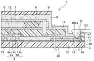
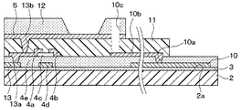
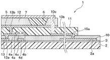
本発明の第1実施形態に係る有機半導体装置1について図1〜図4を参照して説明する。図1、図2に示すように、本実施形態に係る有機半導体装置1は、基板2の一面2a上に、第1絶縁膜3、トランジスタ部4、下部電極5、有機層6、上部電極7、第2絶縁膜8、偏光板9が順次積層されて構成されている。この有機半導体装置1は、下部電極5もしくは上部電極7に接続された配線10がコネクタ100(図3、図4を参照)と電気的に接続させられて、電極(下部電極5または上部電極7)に電圧が印加されると有機層6が発光する発光素子である。すなわち、この有機半導体装置1では、下部電極5、有機層6、および上部電極7によって有機EL素子を構成している。また、有機半導体装置1は、コネクタ100(図1、図2を参照)のターミナルとしてのカンチレバー101(図3、図4を参照)に接触させられる端子部(図1、図2中の一点鎖線20で囲まれた部分)を有する。端子部20は、少なくとも基板2を含む部分である。図2に示すように、この有機半導体装置1では、配線10が、基板2の一面2aのうち端子部20にまで延設されている。(First embodiment)
An
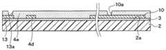
基板2は、ガラス、樹脂、金属等の可視光に対して透明な材料で構成されており、ここでは樹脂を用いて構成されている。図2に示すように、基板2は一面2aおよび一端2bを有し、本実施形態に係る有機半導体装置1では、この基板2の一端2b側において、端子部20が形成されている。 The
図2に示すように、第1絶縁膜3は、外部の湿気が配線10に接触することを抑制するために、基板2の一面2a側に設けられた絶縁膜である。第1絶縁膜3は、基板2の一面2aと配線10との間に設けられている。第1絶縁膜3は、は、ここでは一例として、有機材料を主成分とする有機膜と、該有機膜を挟んで配線10の反対側に配置された無機材料を主成分とする無機膜と、が順に積層された構成とされている。第1絶縁膜3は、例えば、Al2O3で構成された無機膜とAlCHOで構成された有機膜が順に積層された構成とされる。As shown in FIG. 2, the first
図2に示すように、トランジスタ部4は、下部電極5、有機層6、および上部電極7で構成された有機EL素子を駆動するスイッチなどとして設けられたものであり、ソース電極4a、ドレイン電極4b、チャンネル層4c、ゲート絶縁膜4eを有する。チャンネル層4cは、ソース電極4aとドレイン電極4bの間に形成され、ゲート絶縁膜4eは、ゲート電極4d、チャンネル層4cとゲート電極4dの間に形成され、ゲート電極4dを被覆している。ソース電極4a、ドレイン電極4bは、例えば、Ag、Pb、Sn、Cu、Au等の金属で構成される。チャンネル層4cは、例えば、有機半導体で構成される。なお、ここでは、ゲート電極4dは、配線10と同時に形成された膜である。また、図2に示すように、第1絶縁膜3上には、ソース電極4aに接続された配線13が形成されており、この配線13も、ゲート電極4dや配線10と同時に形成された膜である。また、ゲート絶縁膜4eは、ここでは一例として、有機材料を主成分とする有機膜と、該有機膜を挟んで配線10の反対側に配置された無機材料を主成分とする無機膜と、が順に積層された構成とされている。ゲート絶縁膜4eは、例えば、Al2O3で構成された無機膜とAlCHOで構成された有機膜が順に積層された構成とされる。As shown in FIG. 2, the
また、図2に示すように、本実施形態に係る有機半導体装置1では、ゲート絶縁膜4eと下部電極5の間に配置されて、ソース電極4a、ドレイン電極4b、チャンネル層4c、ゲート絶縁膜4eを被覆して保護する保護膜11が形成されている。保護膜11は、ポリマー等で構成される。 As shown in FIG. 2, in the
図2に示すように、ゲート絶縁膜4eは、ゲート電極4dを封止しつつ、端子部20における配線10の上方にまで延設されるように一体に成形されている。これにより、本実施形態に係る有機半導体装置1では、端子部20における配線10が、ゲート絶縁膜4eによって被覆されている。 As shown in FIG. 2, the
下部電極5は、有機EL素子に用いられる電極として設けられたものであり、図2に示すように、ここでは、発光素子における陽極として用いられる電極として保護膜11上に設けられている。下部電極5は、例えば、インジウム−スズの酸化物(ITO)やインジウム−亜鉛の酸化物等の透明導電膜を用いて構成される。図2に示すように、下部電極5は、所定方向(本実施形態では、図2における紙面左右方向)に延びるストライプ状となるように形成されている。また、下部電極5は、ソース電極4aと電気的に接続されている。 The
有機層6は、通常の有機EL素子における有機層の構成と同様な周知なものであり、例えば、下部電極5側から正孔注入層、正孔輸送性層、発光層、電子輸送層等が順次積層されて構成される。また、図2に示すように、有機層6は、下部電極5の所定領域上に形成されている。具体的には、本実施形態に係る有機半導体装置1では、図示しないが、複数の有機層6がバンク12によって互いに区画されている。バンク12は、例えば、ポリイミド等で構成される。 The
上部電極7は、発光素子における陰極として用いられる電極であって、図2に示すように、ここでは、発光素子における陰極として用いられる電極として有機層6やバンク12の上方に設けられている。上部電極7は、例えば、MgAg、Al等の金属膜等を用いて構成されている。図2に示すように、上部電極7は、各有機層6を跨ぐように下部電極5の延設方向と垂直方向に延びるストライプ状となるように形成されている。これにより、下部電極5と上部電極7との交差部において、下部電極5、有機層6、上部電極7が積層されて有機EL素子が形成されている。また、上部電極7は、配線10と電気的に接続されており、図2とは別断面においてドレイン電極4bと電気的に接続されている。 The
第2絶縁膜8は、下部電極5、有機層6、上部電極7などを封止するために設けられた絶縁膜である。第2絶縁膜8は、ここでは一例として、有機材料を主成分とする有機膜と、該有機膜を挟んで配線10の反対側に配置された無機材料を主成分とする無機膜と、が順に積層された構成とされている。第2絶縁膜8は、例えば、Al2O3で構成された無機膜とAlCHOで構成された有機膜が順に積層された構成とされる。図2に示すように、第2絶縁膜8は、少なくとも上部電極7の上方に配置され、下部電極5、有機層6、および上部電極7を封止している。なお、ここでは特に、図2に示すように、第2絶縁膜8は、下部電極5、有機層6、および上部電極7で構成された有機EL素子を基板2との間に挟み込んでおり、この有機EL素子の全面が外部に露出しないように構成されている。The second
なお、上記したように、本実施形態では、第1絶縁膜3、ゲート絶縁膜4e、第2絶縁膜8は、それぞれ、有機材料を主成分とする有機膜と、該有機膜を挟んで配線10の反対側に配置された無機材料を主成分とする無機膜とが順に積層された構成とされている。ここで、これらの膜3、4e、8を有機膜のみによって構成した場合には、有機材料が水分を吸収し易いことにより、有機半導体装置1の周囲の水分が膜3、4e、8に吸収されて配線10にまで到達し易くなってしまう。しかしながら、本実施形態に係る有機半導体装置1では、膜3、4e、8が、水分を透過し難い無機膜によって有機膜が被覆された構成とされているため、有機半導体装置1の周囲の水分が配線10に到達し難くなる。さらに、無機膜は有機膜と比較して硬いことから、本実施形態に係る有機半導体装置1では、有機膜への応力緩和も図ることができる。このように、本実施形態に係る有機半導体装置1では、これらの膜3、4e、8が有機膜を含む構成とされつつ、無機膜も備えられることにより、水分が配線10に到達し難くなり、かつ、有機膜への応力緩和も図ることができる。 As described above, in the present embodiment, the first insulating
第2絶縁膜8は、上部電極5、有機層6、および上部電極7を封止しつつ、端子部20における配線10の上方にまで延設されて形成されている。具体的には、本実施形態では、第2絶縁膜8は、端子部20における配線10の上方に形成されたゲート絶縁膜4eの上方に形成されて、端子部20における配線10を被覆している。 The second
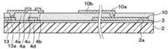
ここで、上記したように、本実施形態に係る有機半導体装置1では、ゲート絶縁膜4eおよび第2絶縁膜8が、端子部20における配線10の上方にまで延設されるように一体に成形されている。すなわち、本実施形態に係る有機半導体装置1では、端子部20における配線10の上方にゲート絶縁膜4eおよび第2絶縁膜8を含む膜が形成されている。そして、本実施形態に係る有機半導体装置1では、ゲート絶縁膜4eおよび第2絶縁膜8を含む膜が、カンチレバー101によって所定方向(図4中の矢印Dを参照)に貫通させられることで配線10とコネクタ100との電気的接続が行われる厚さに設定されている。具体的には、ここでは、端子部20における配線10の上方に形成されたゲート絶縁膜4eおよび第2絶縁膜8を含む膜の厚さが、1〜999nmとされている。 Here, as described above, in the
このため、本実施形態に係る有機半導体装置1では、導通させる(コネクタ100を接触させる)前においては、端子部20における配線10がゲート絶縁膜4eや第2絶縁膜8によって覆われているため、配線10への水分の接触が抑制される。さらに、導通させた(コネクタ100を接触させた)後においても、図4に示すように、端子部20における配線10がゲート絶縁膜4eや第2絶縁膜8によって覆われているため、配線10への水分の接触が抑制される。また、導通させるときには、コネクタ100によって第2絶縁膜8が貫通させられることで配線10とコネクタ100との電気的接続が行われる。このように、本実施形態に係る有機半導体装置1では、配線10とコネクタ100との電気的接続が可能であると共に、端子部20における配線10への水分の接触を抑制でき、マイグレーションの発生を抑制することができる。なお、本実施形態に係る有機半導体装置1では、基板2の一面2aと配線10との間に、外部の湿気が配線10に接触することを抑制する第1絶縁膜3が設けられているため、マイグレーションの発生をさらに抑制できる。 For this reason, in the
また、本実施形態に係る有機半導体装置1では、端子部20における配線10の上方に形成された膜(ゲート絶縁膜4eおよび第2絶縁膜8を含む膜)の厚さが1〜999nmと薄いため、コネクタ100のうち配線10に接触させられる部分(接触凸部101a)が該膜を十分に貫通して配線10に到達させ易い。さらに、端子部20における配線10の上方に形成された膜が薄いことにより、熱応力が発生し難いという利点もある。すなわち、本実施形態に係る有機半導体装置1では、端子部20における配線10の上方に形成された膜における経時的なクラックが生じ難く、また、端子部20における配線10の上方に形成された膜に発生する熱応力によって基板2等が反ってしまう等の不具合が生じ難い。 In the
偏光板9は、外光反射を防ぐために設けられたものであって、外部から有機半導体装置1の内部に進入して有機半導体装置1の内部(例えば、下部電極5や上部電極7)で反射した光を吸収するものである。なお、ここでは、具体的には、偏光板9は円偏光板である。 The
図3に示すように、本実施形態に係る有機半導体装置1に電気的に接続されるコネクタ100は、ここでは、ターミナルとしてのカンチレバー101を有する。また、コネクタ100は、カンチレバー101において、配線10に接触させられる部分である接触凸部101aを有する構成のものである。 As shown in FIG. 3, the
そして、図4に示すように、本有機半導体装置1では、端子部20における配線10の上方に配置されたゲート絶縁膜4eおよび第2絶縁膜8を含む膜の所定方向Dにおける厚さ(図4中の符号t1を参照)が、コネクタ100の接触凸部101aの所定方向Dにおける厚さ(図4中の符号t2を参照)よりも薄くされている。言い換えると、端子部20における配線10にコネクタ100の接触凸部101aを接触させたときに、この膜とコネクタ100(カンチレバー101)との間に隙間(図4中の符号w1を参照)ができる構成とされている。このため、コネクタ100の接触凸部101aを配線10に接触させるときに、配線10の上方に配置された膜(ゲート絶縁膜4eおよび第2絶縁膜8を含む膜)が高温となって熱膨張していても、接触凸部101aが下部電極5に届かないという事態が生じ難い。よって、本実施形態では、有機半導体装置1とコネクタ100とを確実に導通させることができる。 As shown in FIG. 4, in the
上記したように、本実施形態に係る有機半導体装置1では、ゲート絶縁膜4eおよび第2絶縁膜8が、端子部20における配線10の上方にまで延設されるように一体に成形されている。すなわち、本実施形態に係る有機半導体装置1では、端子部20における配線10の上方にゲート絶縁膜4eおよび第2絶縁膜8を含む膜が形成されている。そして、本実施形態に係る有機半導体装置1では、ゲート絶縁膜4eおよび第2絶縁膜8を含む膜が、カンチレバー101によって所定方向Dに貫通させられることで配線10とコネクタ100との電気的接続が行われる厚さに設定されている。 As described above, in the
このため、本実施形態に係る有機半導体装置1では、導通させる(コネクタ100を接触させる)前においては、端子部20における配線10がゲート絶縁膜4eや第2絶縁膜8によって覆われているため、配線10への水分の接触が抑制される。さらに、導通させた(コネクタ100を接触させた)後においても、端子部20における配線10がゲート絶縁膜4eや第2絶縁膜8によって覆われているため、配線10への水分の接触が抑制される。また、導通させるときには、コネクタ100によって第2絶縁膜8が貫通させられることで配線10とコネクタ100との電気的接続が行われる。このように、本実施形態に係る有機半導体装置1では、配線10とコネクタ100との電気的接続が可能であると共に、端子部20における配線10への水分の接触を抑制でき、マイグレーションの発生を抑制することができる。 For this reason, in the
また、本実施形態に係る有機半導体装置1では、端子部20における配線10の上方に形成された膜(ゲート絶縁膜4eおよび第2絶縁膜8を含む膜)の厚さが1〜999nmとされている。 In the
このように、本実施形態に係る有機半導体装置1では、端子部20における配線10の上方に形成された膜の厚さが薄いため、コネクタ100のうち配線10に接触させられる部分(接触凸部101a)が該膜を十分に貫通して配線10に到達させ易い。さらに、端子部20における配線10の上方に形成された膜が薄いことにより、熱応力が発生し難いという利点もある。すなわち、本実施形態に係る有機半導体装置1では、端子部20における配線10の上方に形成された膜における経時的なクラックが生じ難く、また、端子部20における配線10の上方に形成された膜に発生する熱応力によって基板2等が反ってしまう等の不具合が生じ難い。 Thus, in the
以上、本実施形態に係る有機半導体装置1の構成および作用効果について説明した。次に、本実施形態に係る有機半導体装置1の製造方法について図5を参照しつつ説明する。 The configuration and operational effects of the
まず、図5(a)に示すように、基板2の一面2a側に、ALD(Atomic Layer Deposition:原子層堆積)法、CVD(Chemical Vapor Deposition:化学気相成長)法等により、第1絶縁膜3を形成する。ここでは、ALD法によって、第1絶縁膜3を形成している。 First, as shown in FIG. 5A, the first insulation is formed on the
次に、図5(b)に示すように、第1絶縁膜3の上面に、印刷等によって、ゲート電極4d、配線10、および配線13を同時に形成する。これが、特許請求の範囲に記載のゲート電極形成工程に相当する。 Next, as shown in FIG. 5B, the
次に、図5(c)に示すように、第1絶縁膜3、ゲート電極4d、配線10、および配線13を被覆するように、ALD法、CVD法等により、ゲート絶縁膜4eを形成する。ここでは、ALD法によって、ゲート絶縁膜4eを形成している。ここで、本製造方法では、端子部20における配線10の上方に、端子部20(図2中の一点鎖線20で囲まれた部分を参照)における配線10を被覆する一体成形されたゲート絶縁膜4eを形成している。これが、特許請求の範囲に記載のゲート絶縁膜形成工程に相当する。 Next, as shown in FIG. 5C, the
次に、図5(d)に示すように、フォトリソグラフィ等を用いて、ゲート絶縁膜4eにおいて、配線10と後述する配線(図5(f)〜(l)中の符号10bを参照)とを電気的に接続するための第1ビア(図5(d)中の符号10aを参照)、配線13とソース電極4aとを電気的に接続するための第2ビア(図5(d)中の符号13aを参照)を形成する。 Next, as shown in FIG. 5D, using photolithography or the like, in the
次に、図5(e)に示すように、ゲート絶縁膜4eの上面に、印刷等によって、チャンネル層4cを形成する。 Next, as shown in FIG. 5E, a
次に、図5(f)に示すように、印刷等によって、ソース電極4a、ドレイン電極4b、上部電極7と配線10とを電気的に接続するための配線(図5(f)中の符号10bを参照)を同時に形成する。 Next, as shown in FIG. 5 (f), wiring for electrically connecting the
次に、図5(g)に示すように、第1絶縁膜3、ソース電極4a、ドレイン電極4b、チャンネル層4c、ゲート電極4d、および配線10bを被覆もしくは封止するように、印刷等により、保護膜11を形成する。ここでは、ALD法によって、保護膜11を形成している。 Next, as shown in FIG. 5G, the first insulating
次に、図5(h)に示すように、フォトリソグラフィ等を用いて、ゲート絶縁膜4eにおいて、ソース電極4aと下部電極5とを電気的に接続するための第3ビア(図5(h)中の符号13bを参照)を形成する。 Next, as shown in FIG. 5H, a third via for electrically connecting the
次に、図5(i)に示すように、保護膜11の上面に、スパッタやフォトリソグラフィ等により、下部電極5を形成する。これが、特許請求の範囲に記載の第1工程に相当する。また、スパッタやフォトリソグラフィ等により、バンク12を形成する。また、フォトリソグラフィ等を用いて、バンク12および保護膜11において、上部電極7と配線10bとを電気的に接続するための第4ビア(図5(i)中の符号10cを参照)を形成する。 Next, as shown in FIG. 5I, the
次に、図5(j)に示すように、印刷、真空蒸着法等により、有機層6を形成する。これが、特許請求の範囲に記載の第2工程に相当する。 Next, as shown in FIG. 5 (j), the
次に、図5(k)に示すように、有機層6およびバンク12の上面に、蒸着等により、上部電極7を形成する。これが、特許請求の範囲に記載の第3工程に相当する。 Next, as shown in FIG. 5K, the
次に、図5(l)に示すように、有機層6、保護膜11、バンク12、ゲート絶縁膜4e等の上面に、ALD法、CVD法等により、下部電極5、有機層6、および上部電極7を封止する第2絶縁膜8を形成する。ここでは、ALD法によって、第2絶縁膜8を形成している。ここで、本製造方法では、端子部20における配線10の上方に、端子部20における配線10を封止する一体成形された第2絶縁膜8を形成している。厳密には、本製造方法では、端子部20における配線10の上方に形成されたゲート絶縁膜4eの上方に、第2絶縁膜8を形成している。これが、特許請求の範囲に記載の第4工程に相当する。 Next, as shown in FIG. 5 (l), the
ここで、上記したように、本製造方法では、端子部20における配線10の上方に、端子部20における配線10を被覆する一体成形されたゲート絶縁膜4eを形成している。また、端子部20における配線10の上方に形成されたゲート絶縁膜4eの上方に、第2絶縁膜8を形成している。そして、本製造方法では、端子部20における配線10の上方に形成されたゲート絶縁膜4eおよび第2絶縁膜8を含む膜の厚さがカンチレバー101によって所定方向Dに貫通させられる厚さとなるように、ゲート絶縁膜4eおよび第2絶縁膜8を形成している。具体的には、ここでは、端子部20における配線10の上方に形成されたゲート絶縁膜4eおよび第2絶縁膜8を含む膜の厚さが1〜999nmとなるように、ゲート絶縁膜4eおよび第2絶縁膜8を形成している。 Here, as described above, in this manufacturing method, the integrally formed
また、上記したように、本製造方法では、ALD法によって、端子部20における配線10を被覆する膜(ゲート絶縁膜4eおよび第2絶縁膜8を含む膜)を形成している。ALD法によれば、成膜対象の形状、位置によらず均一な膜厚が得られるため、ゲート絶縁膜4eや第2絶縁膜8が形成される。すなわち、ALD法を用いた場合には、ゲート絶縁膜4eや第2絶縁膜8においてピンホールなどの欠陥が形成され難く、これにより、本製造方法で製造される有機半導体装置1では、特に、配線10への水分の接触が抑制され、マイグレーションの発生を抑制できる。 Further, as described above, in this manufacturing method, the film (the film including the
その後、図2に示すように、第2絶縁膜8の上面に偏光板9を備え付ける。 Thereafter, as shown in FIG. 2, a
以上の工程を経て、本実施形態に係る有機半導体装置1は完成する。このように、本製造方法では、一体成形により、容易に、マイグレーションの発生を抑制する第2絶縁膜8を備える有機半導体装置1を製造することができる。 Through the above steps, the
上記で説明したように、本実施形態に係る有機半導体装置1では、ゲート絶縁膜4eおよび第2絶縁膜8が、端子部20における配線10の上方にまで延設されるように一体に成形されている。すなわち、本実施形態に係る有機半導体装置1では、端子部20における配線10の上方にゲート絶縁膜4eおよび第2絶縁膜8を含む膜が形成されている。そして、本実施形態に係る有機半導体装置1では、ゲート絶縁膜4eおよび第2絶縁膜8を含む膜が、カンチレバー101によって所定方向に貫通させられることで配線10とコネクタ100との電気的接続が行われる厚さに設定されている。 As described above, in the
このため、本実施形態に係る有機半導体装置1では、導通させる前においては、端子部20における配線10がゲート絶縁膜4eや第2絶縁膜8によって覆われているため、配線10への水分の接触が抑制される。さらに、導通させた後においても、端子部20における配線10がゲート絶縁膜4eや第2絶縁膜8によって覆われているため、配線10への水分の接触が抑制される。また、導通させるときには、コネクタ100によって第2絶縁膜8が貫通させられるが、ゲート絶縁膜4eおよび第2絶縁膜8を含む膜が薄いため、コネクタ100のうち配線10に接触させられる部分が該膜を十分に貫通して配線10に到達し易い。このように、本実施形態に係る有機半導体装置1では、端子部20における配線10への水分の接触が抑制されるため、マイグレーションの発生を抑制できる。また、ゲート絶縁膜4eおよび第2絶縁膜8を含む膜が薄いことから、配線10とコネクタ100とを十分に接触させられ、確実に電気的接続を実現することができる。 For this reason, in the
また、本実施形態に係る有機半導体装置1では、第1絶縁膜3、ゲート絶縁膜4e、第2絶縁膜8は、それぞれ、有機材料を主成分とする有機膜と、該有機膜を挟んで配線10の反対側に配置された無機材料を主成分とする無機膜とが順に積層された構成とされている。 In the
このため、本実施形態に係る有機半導体装置1では、これらの膜3、4e、8が有機膜を含む構成とされつつ、無機膜も備えられることにより、水分が配線10に到達し難くなり、かつ、有機膜への応力緩和も図ることができる。 For this reason, in the
(他の実施形態)
本発明は上記した実施形態に限定されるものではなく、特許請求の範囲に記載した範囲内において適宜変更が可能である。(Other embodiments)
The present invention is not limited to the embodiment described above, and can be appropriately changed within the scope described in the claims.
例えば、第1実施形態に係る有機半導体装置1では、第1絶縁膜3を設けていたが、例えば基板2の水分不透過性が十分である場合等には、第1絶縁膜3を省略してもよい。 For example, although the first insulating
また、第1実施形態に係る有機半導体装置1では、端子部20における配線10の上方にゲート絶縁膜4eおよび第2絶縁膜8を含む膜を形成して、端子部20における配線10を被覆していた。しかし、端子部20における配線10の上方に形成されて端子部20における配線10を被覆する膜は、この構成に限られるものではない。すなわち、例えば、第1実施形態に係る有機半導体装置1において、ゲート絶縁膜4eを端子部20における配線10の上方にまで延設しないようにして、端子部20における配線10の上方に、ゲート絶縁膜4eを含まず第2絶縁膜8を含み、カンチレバー101によって所定方向Dに貫通させられる厚さ(例えば、1〜999nm)の膜を形成してもよい。この場合においても、第2絶縁膜8を含む膜によって、端子部20における配線10への水分の接触が抑制されるため、マイグレーションの発生を抑制でき、膜が薄いことから、配線10とコネクタ100とを十分に接触させられ易い。また、第1実施形態に係る有機半導体装置1において、第2絶縁膜8を端子部20における配線10の上方にまで延設しないようにして、端子部20における配線10の上方に、第2絶縁膜8を含まずゲート絶縁膜4eを含み、カンチレバー101によって所定方向Dに貫通させられる厚さ(例えば、1〜999nm)の膜を形成してもよい。この場合においても、ゲート絶縁膜4eを含む膜によって、端子部20における配線10への水分の接触が抑制されるため、マイグレーションの発生を抑制でき、膜が薄いことから、配線10とコネクタ100とを十分に接触させられ易い。 In the
また、第1実施形態において、第1絶縁膜3、ゲート絶縁膜4e、第2絶縁膜8のうち、いずれかのみを、有機材料を主成分とする有機膜と、該有機膜を挟んで配線10の反対側に配置された無機材料を主成分とする無機膜とが順に積層された構成としてもよい。 Further, in the first embodiment, only one of the first insulating
2 基板
3 第1絶縁膜3
4 トランジスタ部
4e ゲート絶縁膜
5 下部電極
6 有機層
7 上部電極
8 第2絶縁膜
20 端子部
100 コネクタ2
4
Claims (10)
Translated fromJapanese前記基板の一面側に形成された下部電極(5)と、
前記下部電極の所定領域上に形成された有機層(6)と、
前記有機層上に形成された上部電極(7)と、
少なくとも前記上部電極の上方に配置されて、前記下部電極、前記有機層、および前記上部電極を封止する絶縁膜(8)と、
ゲート電極(4d)および前記ゲート電極を被覆するゲート絶縁膜(4e)を有するトランジスタ部(4)と、を備えると共に、
前記基板の一端側において、ターミナル(101)を有するコネクタ(100)の前記ターミナルに接触させられる部分として構成された端子部(20)を有し、
前記下部電極もしくは前記上部電極に接続された配線(10)が、前記端子部における前記一面の上方にまで延設されており、
前記端子部における前記配線が前記コネクタと電気的に接続させられて、前記下部電極または前記上部電極に電圧が印加されると、前記有機層が発光する有機半導体装置であって、
前記絶縁膜は、前記端子部において前記配線を被覆しており、
前記ゲート絶縁膜は、前記ゲート電極を封止しつつ、前記端子部における前記配線の上方にまで延設されて形成され、前記端子部において前記配線をすべて被覆しており、
前記端子部において前記配線の上方に配置されて前記配線を被覆する前記絶縁膜および前記ゲート絶縁膜を含む膜の厚さ(t1)が、前記ターミナルによって前記絶縁膜および前記ゲート絶縁膜を含む膜が所定方向(D)に貫通させられることで前記配線と前記コネクタとの電気的接続が行われる厚さに設定されていることを特徴とする有機半導体装置。A substrate (2) having one side (2a) and one end (2b);
A lower electrode (5) formed on one side of the substrate;
An organic layer (6) formed on a predetermined region of the lower electrode;
An upper electrode (7) formed on the organic layer;
An insulating film (8) disposed at least above the upper electrode and sealing the lower electrode, the organic layer, and the upper electrode;
A transistor portion (4) having a gate electrode (4d) and a gate insulating film (4e) covering the gate electrode,
On one end side of the substrate, the connector (100) having the terminal (101) has a terminal portion (20) configured as a portion to be brought into contact with the terminal,
The wiring (10) connected to the lower electrode or the upper electrode extends to above the one surface of the terminal portion,
When the wiring in the terminal portion is electrically connected to the connector and a voltage is applied to the lower electrode or the upper electrode, the organic layer emits light from the organic layer,
The insulating film covers the wiring in the terminal portion,
The gate insulating film is formed to extend to above the wiring in the terminal portion while sealing the gate electrode, and coversall the wiring in the terminal portion,
The thickness (t1) of the film including theinsulating film and the gate insulating film which is disposed above the wiring in the terminal portion and covers the wiring is a film including theinsulating film and the gate insulating film by the terminal. Is set to a thickness at which electrical connection between the wiring and the connector is performed by allowing the wiring to penetrate in a predetermined direction (D).
前記下側絶縁膜が、有機材料を主成分とする有機膜と、前記有機膜を挟んで前記配線の反対側に配置された無機材料を主成分とする無機膜と、が順に積層された構成とされていることを特徴とする請求項1ないし3のいずれか1つに記載の有機半導体装置。A lower insulating film (3) is disposed between the substrate and the wiring;
The lower insulating film has a structure in which an organic film mainly composed of an organic material and an inorganic film mainly composed of an inorganic material disposed on the opposite side of the wiring with the organic film interposed therebetween are sequentially stacked. The organic semiconductor device according to any one of claims 1 to3 , wherein the organic semiconductor device is configured as follows.
請求項1ないし3のいずれか1つに記載の有機半導体装置の前記ターミナルが、前記配線に接触させられる接触凸部(101a)を有し、
前記端子部において前記配線の上方に配置されて前記配線を被覆する前記ゲート絶縁膜を含む膜の前記所定方向における厚さ(t1)が、前記接触凸部の前記所定方向における厚さ(t2)よりも薄いことを特徴とする有機半導体装置と前記コネクタとの接続構造。A connection structure between the organic semiconductor device according to claim5 and the connector,
The said terminal of the organic-semiconductor device as described in anyone of Claim1 thru | or3 has a contact convex part (101a) made to contact the said wiring,
The thickness (t1) in the predetermined direction of the film including the gate insulating film that is disposed above the wiring and covers the wiring in the terminal portion is the thickness (t2) in the predetermined direction of the contact convex portion. A connection structure between an organic semiconductor device and the connector, wherein the connection structure is thinner.
前記基板の一面側に前記下部電極を形成する第1工程と、
前記下部電極の所定領域上に前記有機層を形成する第2工程と、
前記有機層上に前記上部電極を形成する第3工程と、
前記下部電極、前記有機層、および前記上部電極を封止する前記絶縁膜を形成する第4工程と、を有し、
前記第4工程において、前記上部電極、前記有機層、および前記上部電極を封止しつつ前記端子部における前記配線の上方にまで延設されて前記端子部における前記配線を被覆する前記絶縁膜を含むと共に前記ターミナルによって前記所定方向に貫通させられる厚さとされた膜を形成することを特徴とする有機半導体装置の製造方法。A method for manufacturing an organic semiconductor device according to anyone of claims1 to 4 ,
A first step of forming the lower electrode on one side of the substrate;
A second step of forming the organic layer on a predetermined region of the lower electrode;
A third step of forming the upper electrode on the organic layer;
A fourth step of forming the insulating film that seals the lower electrode, the organic layer, and the upper electrode, and
In the fourth step, the insulating film that extends to above the wiring in the terminal portion and covers the wiring in the terminal portion while sealing the upper electrode, the organic layer, and the upper electrode A method of manufacturing an organic semiconductor device comprising: forming a film including the terminal and having a thickness penetrating in the predetermined direction by the terminal.
前記基板の一面側にゲート電極(4a)を形成するゲート電極形成工程と、
前記基板の一面側において前記ゲート電極を被覆するゲート絶縁膜(4e)を形成するゲート絶縁膜形成工程と、
前記ゲート絶縁膜上に前記下部電極を形成する第1工程と、
前記下部電極の所定領域上に前記有機層を形成する第2工程と、
前記有機層上に前記上部電極を形成する第3工程と、
前記下部電極、前記有機層、および前記上部電極を封止する前記絶縁膜を形成する第4工程と、を有し、
前記ゲート絶縁膜形成工程において、前記上部電極、前記有機層、および前記上部電極を封止しつつ前記端子部における前記配線の上方にまで延設されて前記端子部における前記配線を被覆する前記ゲート絶縁膜を含むと共に前記ターミナルによって前記所定方向に貫通させられる厚さとされた膜を形成する工程、および、前記第4工程において、前記上部電極、前記有機層、および前記上部電極を封止しつつ前記端子部における前記配線の上方にまで延設されて前記端子部における前記配線を被覆する前記絶縁膜を含むと共に前記ターミナルによって前記所定方向に貫通させられる厚さとされた膜を形成する工程のうち少なくとも一方を行うことを特徴とする有機半導体装置の製造方法。A method for producing an organic semiconductor device according to anyone of claims1 to 3 ,
Forming a gate electrode (4a) on one side of the substrate;
Forming a gate insulating film (4e) covering the gate electrode on one surface side of the substrate;
A first step of forming the lower electrode on the gate insulating film;
A second step of forming the organic layer on a predetermined region of the lower electrode;
A third step of forming the upper electrode on the organic layer;
A fourth step of forming the insulating film that seals the lower electrode, the organic layer, and the upper electrode, and
In the gate insulating film forming step, the gate covering the wiring in the terminal portion by extending up to the wiring in the terminal portion while sealing the upper electrode, the organic layer, and the upper electrode In the step of forming a film including an insulating film and having a thickness penetrating in the predetermined direction by the terminal, and in the fourth step, while sealing the upper electrode, the organic layer, and the upper electrode Among the steps of forming a film that extends to above the wiring in the terminal portion and covers the wiring in the terminal portion and has a thickness that is penetrated in the predetermined direction by the terminal A method for manufacturing an organic semiconductor device, comprising performing at least one of the steps.
Priority Applications (1)
| Application Number | Priority Date | Filing Date | Title |
|---|---|---|---|
| JP2014148106AJP6432189B2 (en) | 2014-07-18 | 2014-07-18 | Organic semiconductor device and manufacturing method thereof |
Applications Claiming Priority (1)
| Application Number | Priority Date | Filing Date | Title |
|---|---|---|---|
| JP2014148106AJP6432189B2 (en) | 2014-07-18 | 2014-07-18 | Organic semiconductor device and manufacturing method thereof |
Publications (2)
| Publication Number | Publication Date |
|---|---|
| JP2016024949A JP2016024949A (en) | 2016-02-08 |
| JP6432189B2true JP6432189B2 (en) | 2018-12-05 |
Family
ID=55271554
Family Applications (1)
| Application Number | Title | Priority Date | Filing Date |
|---|---|---|---|
| JP2014148106AExpired - Fee RelatedJP6432189B2 (en) | 2014-07-18 | 2014-07-18 | Organic semiconductor device and manufacturing method thereof |
Country Status (1)
| Country | Link |
|---|---|
| JP (1) | JP6432189B2 (en) |
Families Citing this family (2)
| Publication number | Priority date | Publication date | Assignee | Title |
|---|---|---|---|---|
| JP2020017377A (en)* | 2018-07-24 | 2020-01-30 | 株式会社東海理化電機製作所 | Organic el element |
| JP7622625B2 (en) | 2021-12-28 | 2025-01-28 | 株式会社デンソー | Graphene device and method for producing same |
Family Cites Families (15)
| Publication number | Priority date | Publication date | Assignee | Title |
|---|---|---|---|---|
| JPS6039790A (en)* | 1983-08-11 | 1985-03-01 | 関西日本電気株式会社 | Organic el |
| JPH03116696U (en)* | 1990-03-12 | 1991-12-03 | ||
| JP3817081B2 (en)* | 1999-01-29 | 2006-08-30 | パイオニア株式会社 | Manufacturing method of organic EL element |
| JP2005100685A (en)* | 2003-09-22 | 2005-04-14 | Toshiba Matsushita Display Technology Co Ltd | Display device and manufacturing method of display device |
| JP5276792B2 (en)* | 2006-03-03 | 2013-08-28 | 株式会社半導体エネルギー研究所 | Method for manufacturing semiconductor device |
| JP5335190B2 (en)* | 2006-12-28 | 2013-11-06 | 双葉電子工業株式会社 | Organic EL panel |
| JP2008300612A (en)* | 2007-05-31 | 2008-12-11 | Panasonic Corp | Display device and manufacturing method thereof |
| JP4752818B2 (en)* | 2007-07-06 | 2011-08-17 | ソニー株式会社 | Organic EL display device, electronic device, substrate for organic EL display device, and method for manufacturing organic EL display device |
| JP5111273B2 (en)* | 2008-07-22 | 2013-01-09 | 株式会社ジャパンディスプレイイースト | Organic EL display device |
| US9385238B2 (en)* | 2011-07-08 | 2016-07-05 | Semiconductor Energy Laboratory Co., Ltd. | Transistor using oxide semiconductor |
| JP2013054863A (en)* | 2011-09-01 | 2013-03-21 | Sony Corp | Organic el display device, manufacturing method of organic el display device and electronic apparatus |
| WO2013046545A1 (en)* | 2011-09-26 | 2013-04-04 | パナソニック株式会社 | Method for manufacturing light emitting device, and light emitting device |
| JP2013122836A (en)* | 2011-12-09 | 2013-06-20 | Sony Corp | Display unit, method of manufacturing the same, electronic apparatus, and illumination unit |
| JP5868757B2 (en)* | 2012-03-28 | 2016-02-24 | 株式会社東芝 | THIN FILM TRANSISTOR, ITS MANUFACTURING METHOD, AND DISPLAY DEVICE |
| CN104782230B (en)* | 2012-11-16 | 2016-11-16 | 柯尼卡美能达株式会社 | Translucent electrodes and electronic devices |
- 2014
- 2014-07-18JPJP2014148106Apatent/JP6432189B2/ennot_activeExpired - Fee Related
Also Published As
| Publication number | Publication date |
|---|---|
| JP2016024949A (en) | 2016-02-08 |
Similar Documents
| Publication | Publication Date | Title |
|---|---|---|
| USRE50526E1 (en) | Method for manufacturing light emitting device, and light emitting device | |
| CN107482042B (en) | OLED display substrate and manufacturing method thereof, and OLED display device | |
| US9722204B2 (en) | Display device | |
| US9660007B2 (en) | Display device and method of manufacturing display device | |
| CN118785752A (en) | Display Devices | |
| US12133420B2 (en) | Display device and manufacturing method thereof | |
| KR102105509B1 (en) | Encapsulation structure, display panel and manufacturing method thereof | |
| CN111463236A (en) | display screen | |
| CN114361235A (en) | Display device | |
| KR20170095444A (en) | Display device and the method of manufacturing thereof | |
| US9076980B2 (en) | Organic light-emitting display apparatus and manufacturing method thereof | |
| KR101893281B1 (en) | Light emitting apparatus | |
| JP2017152245A (en) | Display device | |
| WO2019097823A1 (en) | Display device | |
| JP2015173078A (en) | Organic EL display device and organic EL display device manufacturing method | |
| US20170279073A1 (en) | Display device | |
| US20140353671A1 (en) | Display device and manufacturing method thereof | |
| KR20140137713A (en) | Organinc light emitting display device and manufacturing method for the same | |
| JP6432189B2 (en) | Organic semiconductor device and manufacturing method thereof | |
| US11508799B2 (en) | Display device comprising frame region surrounding display region | |
| JP2009277549A (en) | Organic electroluminescent panel and defect detecting method of the same | |
| JP7033679B2 (en) | Light emitting device | |
| CN118660510A (en) | Display device having substrate hole | |
| JP6617024B2 (en) | Light emitting device | |
| JP4823685B2 (en) | EL device and manufacturing method thereof |
Legal Events
| Date | Code | Title | Description |
|---|---|---|---|
| A621 | Written request for application examination | Free format text:JAPANESE INTERMEDIATE CODE: A621 Effective date:20170308 | |
| A131 | Notification of reasons for refusal | Free format text:JAPANESE INTERMEDIATE CODE: A131 Effective date:20180206 | |
| A977 | Report on retrieval | Free format text:JAPANESE INTERMEDIATE CODE: A971007 Effective date:20180207 | |
| A521 | Request for written amendment filed | Free format text:JAPANESE INTERMEDIATE CODE: A523 Effective date:20180402 | |
| TRDD | Decision of grant or rejection written | ||
| A01 | Written decision to grant a patent or to grant a registration (utility model) | Free format text:JAPANESE INTERMEDIATE CODE: A01 Effective date:20181009 | |
| A61 | First payment of annual fees (during grant procedure) | Free format text:JAPANESE INTERMEDIATE CODE: A61 Effective date:20181022 | |
| R151 | Written notification of patent or utility model registration | Ref document number:6432189 Country of ref document:JP Free format text:JAPANESE INTERMEDIATE CODE: R151 | |
| LAPS | Cancellation because of no payment of annual fees |