Movatterモバイル変換


[0]ホーム

URL:


JP6415813B2 - Current sensor, current measurement module and smart meter - Google Patents

Current sensor, current measurement module and smart meter
Download PDF

Info

Publication number
JP6415813B2
JP6415813B2JP2013268067AJP2013268067AJP6415813B2JP 6415813 B2JP6415813 B2JP 6415813B2JP 2013268067 AJP2013268067 AJP 2013268067AJP 2013268067 AJP2013268067 AJP 2013268067AJP 6415813 B2JP6415813 B2JP 6415813B2
Authority
JP
Japan
Prior art keywords
layer
magnetoresistive element
magnetic
linear response
magnetic field
Prior art date
Legal status (The legal status is an assumption and is not a legal conclusion. Google has not performed a legal analysis and makes no representation as to the accuracy of the status listed.)
Active
Application number
JP2013268067A
Other languages
Japanese (ja)
Other versions
JP2015125020A (en
Inventor
祥弘 東
祥弘 東
慶彦 藤
慶彦 藤
福澤 英明
英明 福澤
哲郎 和村
哲郎 和村
元通 芝野
元通 芝野
Current Assignee (The listed assignees may be inaccurate. Google has not performed a legal analysis and makes no representation or warranty as to the accuracy of the list.)
Toshiba Corp
Original Assignee
Toshiba Corp
Priority date (The priority date is an assumption and is not a legal conclusion. Google has not performed a legal analysis and makes no representation as to the accuracy of the date listed.)
Filing date
Publication date
Application filed by Toshiba CorpfiledCriticalToshiba Corp
Priority to JP2013268067ApriorityCriticalpatent/JP6415813B2/en
Priority to EP14198210.8Aprioritypatent/EP2889631A1/en
Priority to US14/580,984prioritypatent/US10254315B2/en
Publication of JP2015125020ApublicationCriticalpatent/JP2015125020A/en
Application grantedgrantedCritical
Publication of JP6415813B2publicationCriticalpatent/JP6415813B2/en
Activelegal-statusCriticalCurrent
Anticipated expirationlegal-statusCritical

Links

Images

Classifications

Landscapes

Description

Translated fromJapanese

本実施の形態は、電流センサ、電流測定モジュール及びこれを搭載したスマートメータに関する。  The present embodiment relates to a current sensor, a current measurement module, and a smart meter equipped with the current sensor.

近年、電力需給の安定化や効率化などを目的として、電力をデジタルで計測し、メーター内に通信機能を持たせた次世代電力量計であるスマートメータの導入が進められようとしている。スマートメータで必要となる広ダイナミックレンジ・高分解能を低消費電力で実現する電流センサが求められている。  In recent years, for the purpose of stabilizing and improving power supply and demand, the introduction of smart meters, which are next-generation watt-hour meters that measure power digitally and have a communication function in the meter, is being promoted. There is a need for a current sensor that achieves the wide dynamic range and high resolution required by smart meters with low power consumption.

高分解能の電流センサを実現するためには、磁場に対する感度の高い磁気抵抗素子を用いることが有効である。また、高分解能と広ダイナミックレンジを両立するために、磁気抵抗素子を用いた磁気平衡方式の電流センサが提案されている。しかし、磁気平衡方式では、被測定電流が大きくなった場合に被測定電流により発生する大きな誘導磁場と同程度のキャンセル磁場をコイルにて発生させる必要がある。この場合、キャンセル磁場を発生させるためにコイルに流す電流は、被測定電流の大きさに比例して大きくなるため、大きな被測定電流の場合には電流センサ自体の消費電力が大きくなってしまうという問題がある。  In order to realize a high-resolution current sensor, it is effective to use a magnetoresistive element having high sensitivity to a magnetic field. In order to achieve both high resolution and a wide dynamic range, a magnetic balance type current sensor using a magnetoresistive element has been proposed. However, in the magnetic balance method, it is necessary to generate a cancel magnetic field in the coil that is about the same as a large induction magnetic field generated by the current to be measured when the current to be measured becomes large. In this case, the current that flows through the coil to generate the canceling magnetic field increases in proportion to the magnitude of the current to be measured, so that in the case of a large current to be measured, the power consumption of the current sensor itself increases. There's a problem.

特開2013−113799号公報JP 2013-113799 A特許5260109号公報Japanese Patent No. 5260109

本実施の形態に係る電流センサ、電流測定モジュール及びスマートメータは、広い測定範囲にわたって高精度な測定を低消費電力で可能とする電流センサ、電流測定モジュール及びスマートメータを提供するものである。  The current sensor, the current measurement module, and the smart meter according to the present embodiment provide a current sensor, a current measurement module, and a smart meter that enable highly accurate measurement with low power consumption over a wide measurement range.

本発明の一の実施の形態に係る電流センサは、被測定電流からの誘導磁界の印加により抵抗値が変化する複数の磁気抵抗素子と、これら複数の磁気抵抗素子から一の磁気抵抗素子を選択し、選択した磁気抵抗素子の抵抗値を出力する選択回路とを有する。前記複数の磁気抵抗素子は、印加された前記誘導磁界の大きさと前記抵抗値との関係が互いに異なる。また、本発明の一の実施の形態に係るスマートメータは、例えば本実施の形態に係る電流センサを搭載している。  A current sensor according to an embodiment of the present invention selects a plurality of magnetoresistive elements whose resistance values change by applying an induced magnetic field from a current to be measured, and one magnetoresistive element from the plurality of magnetoresistive elements And a selection circuit for outputting the resistance value of the selected magnetoresistive element. In the plurality of magnetoresistive elements, the relationship between the magnitude of the applied induction magnetic field and the resistance value is different from each other. Moreover, the smart meter which concerns on one embodiment of this invention mounts the current sensor which concerns on this embodiment, for example.

第1の実施の形態に係る電流センサの構成例を示す概略図である。It is the schematic which shows the structural example of the current sensor which concerns on 1st Embodiment.同実施の形態に係る磁気抵抗素子の概略構成を例示する模式的斜視図である。FIG. 3 is a schematic perspective view illustrating a schematic configuration of a magnetoresistive element according to the same embodiment.同実施の形態に係る磁気抵抗素子の機能について説明するための模式図である。It is a schematic diagram for demonstrating the function of the magnetoresistive element based on the embodiment.同実施の形態に係る磁気抵抗素子を例示する模式的斜視図である。It is a typical perspective view which illustrates the magnetoresistive element concerning the embodiment.同実施の形態の他の構成に係る第1の磁気抵抗素子100Eを例示する模式的斜視図である。It is a typical perspective view which illustrates the 1stmagnetoresistive element 100E concerning other composition of the embodiment.同実施の形態の他の構成に係る第1の磁気抵抗素子100Fを示す模式的斜視図である。It is a typical perspective view showing the 1stmagnetoresistive element 100F concerning other composition of the embodiment.同実施の形態に係る第1の磁気抵抗素子100と、第1の線形応答磁性体160Aの模式図である。It is a schematic diagram of the 1stmagnetoresistive element 100 and the 1st linear responsemagnetic body 160A which concern on the embodiment.同実施の形態に係る電流センサの構成例を示す模式図である。It is a schematic diagram which shows the structural example of the current sensor which concerns on the same embodiment.同実施の形態に係る電流センサの他の構成例を示す模式図である。It is a schematic diagram which shows the other structural example of the current sensor which concerns on the same embodiment.同実施の形態に係る電流センサの他の構成例を示す模式図である。It is a schematic diagram which shows the other structural example of the current sensor which concerns on the same embodiment.同実施の形態に係る電流センサの他の構成例を示す模式図である。It is a schematic diagram which shows the other structural example of the current sensor which concerns on the same embodiment.同実施の形態に係る電流センサの他の構成例を示す模式図である。It is a schematic diagram which shows the other structural example of the current sensor which concerns on the same embodiment.同実施の形態に係る電流センサの構成例を示す模式図である。It is a schematic diagram which shows the structural example of the current sensor which concerns on the same embodiment.同実施の形態に係る第1の磁気抵抗素子100と第1の線形応答磁性体160Gの模式図である。It is a schematic diagram of the 1stmagnetoresistive element 100 and the 1st linear responsemagnetic body 160G which concern on the embodiment.同実施の形態に係る電流センサの他の構成例を示す模式図である。It is a schematic diagram which shows the other structural example of the current sensor which concerns on the same embodiment.同実施の形態に係る電流センサの製造方法を例示する模式的な斜視図である。It is a typical perspective view which illustrates the manufacturing method of the current sensor which concerns on the same embodiment.同実施の形態に係る電流センサの別の製造方法を例示する模式的な斜視図である。It is a typical perspective view which illustrates another manufacturing method of the current sensor concerning the embodiment.第2の実施の形態に係る電流センサの構成を示す模式図である。It is a schematic diagram which shows the structure of the current sensor which concerns on 2nd Embodiment.同電流センサの構成例を示す概略図である。It is the schematic which shows the structural example of the same current sensor.同実施の形態に係る電流センサの構成例を示す模式図である。It is a schematic diagram which shows the structural example of the current sensor which concerns on the same embodiment.同実施の形態に係る電流センサの他の構成例を示す模式図である。It is a schematic diagram which shows the other structural example of the current sensor which concerns on the same embodiment.本実施の形態に係る電流センサの製造方法を例示する模式的な斜視図である。It is a typical perspective view which illustrates the manufacturing method of the current sensor which concerns on this Embodiment.本実施の形態に係る電流センサの別の製造方法を例示する模式的な斜視図である。It is a typical perspective view which illustrates another manufacturing method of the current sensor concerning this embodiment.第3の実施の形態に係る電流センサの構成を示す回路ブロック図である。It is a circuit block diagram which shows the structure of the current sensor which concerns on 3rd Embodiment.同実施の形態に係る電流センサのコンパレータ630の構成を示す回路図である。It is a circuit diagram which shows the structure of thecomparator 630 of the current sensor which concerns on the same embodiment.同実施の形態に係る電流センサの複数の測定用磁気抵抗素子610−1〜610−n及びリファレンス磁気抵抗素子620の特性を示すグラフである。It is a graph which shows the characteristic of the several magnetoresistive element 610-1 to 610-n for a current sensor and the referencemagnetoresistive element 620 of the current sensor which concerns on the same embodiment.同実施の形態に係る電流センサの制御信号の真理値表である。It is a truth table of the control signal of the current sensor according to the same embodiment.同実施の形態に係る電流センサのメモリ680の動作を説明するための回路ブロック図である。It is a circuit block diagram for demonstrating operation | movement of thememory 680 of the current sensor which concerns on the embodiment.第4の実施の形態に係る電流センサコンパレータ639の構成を示す回路図である。It is a circuit diagram which shows the structure of thecurrent sensor comparator 639 which concerns on 4th Embodiment.同実施の形態に係る電流センサの複数の測定用磁気抵抗素子610−1〜610−n及びリファレンス磁気抵抗素子620の特性を示すグラフである。It is a graph which shows the characteristic of the several magnetoresistive element 610-1 to 610-n for a current sensor and the referencemagnetoresistive element 620 of the current sensor which concerns on the same embodiment.同実施の形態に係る電流センサの制御信号の真理値表である。It is a truth table of the control signal of the current sensor according to the same embodiment.同実施の形態に係る電流センサのメモリ680の動作を説明するための回路ブロック図である。It is a circuit block diagram for demonstrating operation | movement of thememory 680 of the current sensor which concerns on the embodiment.測定用磁気抵抗素子及びリファレンス磁気抵抗素子の構成例を示す回路図である。It is a circuit diagram which shows the structural example of the magnetoresistive element for a measurement, and a reference magnetoresistive element.第5の実施の形態に係るスマートメータ700を示す模式図である。It is a schematic diagram which shows thesmart meter 700 which concerns on 5th Embodiment.同スマートメータ700の一部の概略構成を示す模式図である。4 is a schematic diagram showing a schematic configuration of a part of thesmart meter 700. FIG.同スマートメータ700の概略構成を示す機能ブロック図である。2 is a functional block diagram showing a schematic configuration of thesmart meter 700. FIG.第6の実施の形態に係るスマートメータ701を示す模式図である。It is a schematic diagram which shows thesmart meter 701 which concerns on 6th Embodiment.第7の実施の形態に係るスマートメータ702を示す模式図である。It is a schematic diagram which shows thesmart meter 702 which concerns on 7th Embodiment.同スマートメータの他の構成例を示す模式図である。It is a schematic diagram which shows the other structural example of the smart meter.第8の実施の形態に係るスマートメータ703を示す模式図である。It is a schematic diagram which shows thesmart meter 703 which concerns on 8th Embodiment.同スマートメータ703の一部の概略構成を示す模式図である。3 is a schematic diagram showing a schematic configuration of a part of thesmart meter 703. FIG.第9の実施の形態に係るスマートメータ704を示す模式図である。It is a schematic diagram which shows thesmart meter 704 which concerns on 9th Embodiment.第10の実施の形態に係るスマートメータ705を示す模式図である。It is a schematic diagram which shows thesmart meter 705 which concerns on 10th Embodiment.同スマートメータの他の構成例を示す模式図である。It is a schematic diagram which shows the other structural example of the smart meter.第11の実施の形態に係る家庭用電化製品の様子を示す模式図である。It is a schematic diagram which shows the mode of the household electrical appliance which concerns on 11th Embodiment.

[1.第1の実施の形態]
[1−1.全体構成]
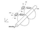
図1は、第1の実施の形態に係る電流センサの構成例を示す概略図である。第1の実施の形態に係る電流センサは、配線500の近傍に配置され、この配線500に流れる測定電流からの誘導磁界の印加により抵抗値が変化する第1の磁気抵抗素子100及び第2の磁気抵抗素子200を有する。第1の磁気抵抗素子100及び第2の磁気抵抗素子200は、それぞれ磁化自由層として動作する第1磁性層101,201及び磁化固定層102,202を有する。また、第1の磁気抵抗素子100及び第2の磁気抵抗素子200は、印加された誘導磁界の大きさと抵抗値との関係が互いに異なる。更に言えば、本実施の形態に係る第1の磁気抵抗素子100及び第2の磁気抵抗素子200は、所定の誘導磁界の増加量に応じた抵抗値の増加量又は減少量が異なる。このような形態の電流センサを用いることによって、広いレンジの電流値に対して高精度な測定を低消費電力で実現することができる。
[1. First Embodiment]
[1-1. overall structure]
FIG. 1 is a schematic diagram illustrating a configuration example of a current sensor according to the first embodiment. The current sensor according to the first embodiment is arranged in the vicinity of thewiring 500, and the firstmagnetoresistive element 100 and the secondmagnetoresistive element 100 whose resistance value changes due to application of an induced magnetic field from a measurement current flowing through thewiring 500. Amagnetoresistive element 200 is included. The firstmagnetoresistive element 100 and thesecond magnetoresistive element 200 have firstmagnetic layers 101 and 201 and magnetization fixedlayers 102 and 202 that operate as magnetization free layers, respectively. Further, the firstmagnetoresistive element 100 and thesecond magnetoresistive element 200 are different from each other in the relationship between the magnitude of the applied induction magnetic field and the resistance value. Furthermore, the firstmagnetoresistive element 100 and thesecond magnetoresistive element 200 according to the present embodiment differ in the amount of increase or decrease in resistance value according to the amount of increase in the predetermined induction magnetic field. By using such a current sensor, highly accurate measurement can be realized with low power consumption for a wide range of current values.

以下、所定の誘導磁界の増加量に応じた抵抗値の増加量又は減少量を磁場感度と呼ぶ。磁場感度は、磁気抵抗素子の抵抗値の変化量をdR、磁気抵抗素子の通常の抵抗値をR、磁気抵抗素子の飽和磁場をHsとすると、(dR/R)/2Hsで表すことが可能である。尚、飽和磁場は、誘導磁場の変化に対し、抵抗値が変化しなくなった時の磁場の大きさである。  Hereinafter, the amount of increase or decrease in resistance according to the amount of increase in the predetermined induction magnetic field is referred to as magnetic field sensitivity. Magnetic field sensitivity can be expressed as (dR / R) / 2Hs, where dR is the amount of change in the resistance value of the magnetoresistive element, R is the normal resistance value of the magnetoresistive element, and Hs is the saturation magnetic field of the magnetoresistive element. It is. The saturation magnetic field is the magnitude of the magnetic field when the resistance value no longer changes with respect to the change of the induction magnetic field.

尚、図1に示した電流センサでは、異なる磁気−抵抗特性を有する2つの磁気抵抗素子100及び200を例示したが、異なる3つ以上の磁気−抵抗特性を有する複数の磁気抵抗素子を用いてもよい。異なる磁気−抵抗特性を有する磁気抵抗素子の数は、測定対象の電流レンジおよび求められる測定分解能に応じて適切に調整することができる。  In the current sensor shown in FIG. 1, twomagnetoresistive elements 100 and 200 having different magneto-resistance characteristics are illustrated, but a plurality of magnetoresistive elements having three or more different magneto-resistance characteristics are used. Also good. The number of magnetoresistive elements having different magneto-resistance characteristics can be appropriately adjusted according to the current range to be measured and the required measurement resolution.

[1−2.動作原理]
図2は、本実施の形態に係る電流センサに用いられる磁気抵抗素子の概略構成を例示する模式的斜視図である。例えば第1の磁気抵抗素子100は、第1磁性層101と、第2磁性層102と、第1磁性層と第2磁性層との間に設けられた中間層103と、図示しない電極層とを含む。尚、第2の磁気抵抗素子200は、第1の磁気抵抗素子100とほぼ同様に構成されている。
[1-2. Operating principle]
FIG. 2 is a schematic perspective view illustrating a schematic configuration of a magnetoresistive element used in the current sensor according to the present embodiment. For example, the firstmagnetoresistive element 100 includes a firstmagnetic layer 101, a secondmagnetic layer 102, anintermediate layer 103 provided between the first magnetic layer and the second magnetic layer, an electrode layer (not shown), including. Thesecond magnetoresistive element 200 is configured in substantially the same manner as the firstmagnetoresistive element 100.

中間層103は、例えば、非磁性層である。第1磁性層101は、例えば、磁化が自由に変化する磁化自由層である。第2磁性層102は、例えば、磁化の固定された磁化固定層である。  Theintermediate layer 103 is, for example, a nonmagnetic layer. The firstmagnetic layer 101 is, for example, a magnetization free layer whose magnetization changes freely. The secondmagnetic layer 102 is, for example, a magnetization fixed layer whose magnetization is fixed.

第1の磁気抵抗素子100は、中間層103が導電材料で形成されている場合はGMR(Giant Magneto Resistance)素子であり、中間層103が絶縁材料で形成されている場合はTMR(Tunneling Magneto Resistance)素子である。第1の磁気抵抗素子100がGMR素子である場合には、電流が膜面垂直方向に通電されるCPP−GMR素子である場合や、電流が膜面内方向に通電されるCIP−GMR素子である場合がある。第1の磁気抵抗素子100がTMR素子である場合には、電流が膜面垂直方向に通電される。また、第1の磁気抵抗素子100は、AMR素子であっても良い。  The firstmagnetoresistive element 100 is a GMR (Giant Magneto Resistance) element when theintermediate layer 103 is formed of a conductive material, and the TMR (Tunneling Magneto Resistance) when theintermediate layer 103 is formed of an insulating material. ) Element. When the firstmagnetoresistive element 100 is a GMR element, it is a CPP-GMR element in which current is passed in the direction perpendicular to the film surface, or a CIP-GMR element in which current is passed in the direction in the film plane. There may be. When the firstmagnetoresistive element 100 is a TMR element, a current is passed in the direction perpendicular to the film surface. The firstmagnetoresistive element 100 may be an AMR element.

図3は、本実施の形態で用いる磁気抵抗素子が磁場を検知する機能について説明する模式図である。以降、第1磁性層101が磁化自由層、第2磁性層102が磁化固定層の場合を例にとり、説明する。  FIG. 3 is a schematic diagram for explaining the function of the magnetic resistance element used in the present embodiment detecting a magnetic field. Hereinafter, the case where the firstmagnetic layer 101 is a magnetization free layer and the secondmagnetic layer 102 is a magnetization fixed layer will be described as an example.

磁気抵抗素子が磁場を検知する機能は「MR効果」に基づく。「MR効果」は、第1磁性層101と中間層103と第2磁性層102との積層膜において発現する。「MR効果」とは、磁性体を有する積層膜において、外部磁界が印加されたときに、磁性体の磁化の変化によって積層膜の電気抵抗の値が変化する現象である。  The function of detecting the magnetic field by the magnetoresistive element is based on the “MR effect”. The “MR effect” is manifested in a laminated film of the firstmagnetic layer 101, theintermediate layer 103, and the secondmagnetic layer 102. The “MR effect” is a phenomenon in which the value of the electrical resistance of the laminated film changes due to a change in magnetization of the magnetic substance when an external magnetic field is applied to the laminated film having a magnetic substance.

図3(b)に示すように第1の磁気抵抗素子100に誘導磁界が加わっていない初期状態では、第1磁性層101と第2磁性層102の磁化方向が所定の角度を有する。第2磁性層102の磁化方向は、後述するように積層方向に隣接する反強磁性層などで固定されており、第1磁性層101の磁化方向は、第1の線形応答磁性体160等や磁界中アニールの方向によって所定の向きに設定される。  As shown in FIG. 3B, in the initial state where no induced magnetic field is applied to the firstmagnetoresistive element 100, the magnetization directions of the firstmagnetic layer 101 and the secondmagnetic layer 102 have a predetermined angle. As will be described later, the magnetization direction of the secondmagnetic layer 102 is fixed by an antiferromagnetic layer or the like adjacent to the stacking direction, and the magnetization direction of the firstmagnetic layer 101 is changed to the first linear responsemagnetic body 160 or the like. A predetermined direction is set depending on the direction of annealing in a magnetic field.

図3(a),(c)に示すように、第1の磁気抵抗素子100に誘導磁界が加わることで、第1磁性層101の磁化方向が変化する。その結果、第1磁性層101と第2磁性層102の磁化方向の相対角度が変化する。  As shown in FIGS. 3A and 3C, the magnetization direction of the firstmagnetic layer 101 is changed by applying an induction magnetic field to the firstmagnetoresistive element 100. As a result, the relative angles of the magnetization directions of the firstmagnetic layer 101 and the secondmagnetic layer 102 change.

第1の磁気抵抗素子100に電流を流すと、磁化方向の相対角度の変化が抵抗変化として表れる。低抵抗状態の抵抗をRとし、MR効果によって変化する電気抵抗の変化量をΔRとしたときに、ΔR/Rを「MR変化率」という。第1磁性層101と中間層103と第2磁性層102の材料の組み合わせによって正の磁気抵抗効果が生ずる場合、第1磁性層101と第2磁性層102の磁化方向の相対角度の減少に伴って電気抵抗が減少する。一方、第1磁性層101と中間層103と第2磁性層102の材料の組み合わせによって負の磁気抵抗効果が生ずる場合、第1磁性層101と第2磁性層102の磁化方向の相対角度の減少に伴って電気抵抗が増大する。  When a current is passed through the firstmagnetoresistive element 100, a change in the relative angle of the magnetization direction appears as a resistance change. ΔR / R is referred to as “MR change rate”, where R is the resistance in the low resistance state and ΔR is the amount of change in electrical resistance that changes due to the MR effect. When a positive magnetoresistance effect is generated by the combination of the materials of the firstmagnetic layer 101, theintermediate layer 103, and the secondmagnetic layer 102, the relative angle of the magnetization direction of the firstmagnetic layer 101 and the secondmagnetic layer 102 decreases. Electric resistance decreases. On the other hand, when a negative magnetoresistance effect is generated by the combination of the materials of the firstmagnetic layer 101, theintermediate layer 103, and the secondmagnetic layer 102, the relative angle of the magnetization direction of the firstmagnetic layer 101 and the secondmagnetic layer 102 is decreased. As a result, the electrical resistance increases.

図3(d)に示す例では、正の磁気抵抗効果を例にとっている。GMR素子やTMR素子などの磁気抵抗素子では、「MR変化率」が非常に大きいため、ホール素子などに比べて、磁界に対する感度が高い。また、磁気抵抗素子では、図3(d)に例示するとおり、磁化自由層と磁化固定層が平行の場合が抵抗の最小値、反平行である場合が抵抗の最大値とした、磁場に対する電気抵抗変化のダイナミックレンジが存在する。図3(d)に示したとおり、磁気抵抗素子のダイナミックレンジは2Hsで定義される。  In the example shown in FIG. 3D, the positive magnetoresistance effect is taken as an example. A magnetoresistive element such as a GMR element or a TMR element has a very large “MR change rate” and therefore has higher sensitivity to a magnetic field than a Hall element or the like. In the magnetoresistive element, as illustrated in FIG. 3D, the electric resistance against the magnetic field is set such that the minimum value of resistance is obtained when the magnetization free layer and the magnetization fixed layer are parallel, and the maximum value of resistance is obtained when the magnetization free layer is antiparallel. There is a dynamic range of resistance change. As shown in FIG. 3D, the dynamic range of the magnetoresistive element is defined by 2Hs.
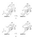
[1−3.磁気抵抗素子の構成例]
以下、本実施の形態に係る磁気抵抗素子の構成例について説明する。図4(a)〜図4(d)は、本実施の形態に係る電流センサに用いられる磁気抵抗素子を例示する模式的斜視図である。尚、以下において、「材料A/材料B」の記載は、材料Aの層の上に、材料Bの層が設けられている状態を示す。尚、以下の説明においては第1の磁気抵抗素子100を例として説明するが、第2の磁気抵抗素子200も同様に構成することが可能であり、更に磁気抵抗素子を設ける場合にも、同様に構成することが可能である。
[1-3. Example of magnetoresistive element configuration]
Hereinafter, a configuration example of the magnetoresistance element according to the present exemplary embodiment will be described. FIG. 4A to FIG. 4D are schematic perspective views illustrating a magnetoresistive element used in the current sensor according to this embodiment. In the following description, “material A / material B” indicates a state in which a layer of material B is provided on a layer of material A. In the following description, the firstmagnetoresistive element 100 will be described as an example. However, thesecond magnetoresistive element 200 can be configured in the same manner. It is possible to configure.

図4(a)は、所定の実施の形態に用いられる第1の磁気抵抗素子100Aを例示する模式的斜視図である。図4(a)に表したように、第1の磁気抵抗素子100Aは、順に並べられた、下部電極E1と、下地層104と、ピニング層105と、第2磁化固定層106と、磁気結合層107と、第2磁性層102と、中間層103と、第1磁性層101と、キャップ層108と、上部電極E2とを含む。  FIG. 4A is a schematic perspective view illustrating the firstmagnetoresistive element 100A used in the predetermined embodiment. As shown in FIG. 4A, the firstmagnetoresistive element 100A includes a lower electrode E1, anunderlayer 104, a pinninglayer 105, a second magnetization fixedlayer 106, and a magnetic coupling arranged in order. Thelayer 107, the secondmagnetic layer 102, theintermediate layer 103, the firstmagnetic layer 101, thecap layer 108, and the upper electrode E2 are included.

この例では、第1磁性層101は磁化自由層として機能し、第2磁性層102は第1磁化固定層として機能する。図4(a)の第1の磁気抵抗素子100Aは、ボトムスピンバルブ型と呼ばれる。  In this example, the firstmagnetic layer 101 functions as a magnetization free layer, and the secondmagnetic layer 102 functions as a first magnetization fixed layer. The firstmagnetoresistive element 100A in FIG. 4A is called a bottom spin valve type.

下地層104には、例えば、Ta/Ruが用いられる。このTa層の厚さ(Z軸方向の長さ)は、例えば、3nmである。このRu層の厚さは、例えば、2nmである。ピニング層105には、例えば、7nmの厚さのIrMn層が用いられる。第2磁化固定層106には、例えば、2.5nmの厚さのCo75Fe25層が用いられる。磁気結合層107には、例えば、0.9nmの厚さのRu層が用いられる。第1磁化固定層102には、例えば、3nmの厚さのCo40Fe4020層が用いられる。中間層103には、例えば、1.6nmの厚さのMgO層が用いられる。第1磁性層101には、例えば、Co40Fe4020/Ni80Fe20が用いられる。2nmの厚さのCo40Fe4020と8nmの厚さのNi80Fe20の積層体が用いられる。キャップ層108には、例えばTa/Ruが用いられる。このTa層の厚さは、例えば、1nmである。このRu層の厚さは、例えば、5nmである。For example, Ta / Ru is used for theunderlayer 104. The thickness of this Ta layer (the length in the Z-axis direction) is, for example, 3 nm. The thickness of this Ru layer is 2 nm, for example. For the pinninglayer 105, for example, an IrMn layer having a thickness of 7 nm is used. For the second magnetization fixedlayer 106, for example, a Co75 Fe25 layer having a thickness of 2.5 nm is used. For themagnetic coupling layer 107, for example, a Ru layer having a thickness of 0.9 nm is used. For the first magnetization fixedlayer 102, for example, a Co40 Fe40 B20 layer having a thickness of 3 nm is used. For theintermediate layer 103, for example, an MgO layer having a thickness of 1.6 nm is used. For the firstmagnetic layer 101, for example, Co40 Fe40 B20 / Ni80 Fe20 is used. A stack of Co40 Fe40 B20 with a thickness of 2 nm and Ni80 Fe20 with a thickness of 8 nm is used. For example, Ta / Ru is used for thecap layer 108. The thickness of this Ta layer is 1 nm, for example. The thickness of this Ru layer is 5 nm, for example.

下部電極E1及び上部電極E2には、例えば、アルミニウム(Al)、アルミニウム銅合金(Al−Cu)、銅(Cu)、銀(Ag)、及び、金(Au)の少なくともいずれかが用いられる。下部電極E1及び上部電極E2として、このような電気抵抗が比較的小さい材料を用いることで、第1の磁気抵抗素子100Aに効率的に電流を流すことができる。  For example, at least one of aluminum (Al), aluminum copper alloy (Al-Cu), copper (Cu), silver (Ag), and gold (Au) is used for the lower electrode E1 and the upper electrode E2. By using such a material having a relatively small electric resistance as the lower electrode E1 and the upper electrode E2, a current can be efficiently passed through the firstmagnetoresistive element 100A.

下部電極E1は、下部電極E1用の下地層(図示せず)と、キャップ層(図示せず)と、の間に、Al、Al−Cu、Cu、Ag、及び、Auの少なくともいずれかの層が設けられた構造を有しても良い。例えば、下部電極E1には、タンタル(Ta)/銅(Cu)/タンタル(Ta)などが用いられる。下部電極E1用の下地層としてTaを用いることで、例えば、下部電極E1を構成する層間の密着性を向上させることができる。下部電極E1用の下地層として、チタン(Ti)、または、窒化チタン(TiN)などを用いても良い。下部電極E1用のキャップ層としてTaを用いることで、そのキャップ層の下の銅(Cu)などの酸化を防ぐことができる。下部電極E1用のキャップ層として、チタン(Ti)、または、窒化チタン(TiN)などを用いても良い。  The lower electrode E1 includes at least one of Al, Al—Cu, Cu, Ag, and Au between a base layer (not shown) for the lower electrode E1 and a cap layer (not shown). You may have the structure in which the layer was provided. For example, tantalum (Ta) / copper (Cu) / tantalum (Ta) is used for the lower electrode E1. By using Ta as the base layer for the lower electrode E1, for example, the adhesion between the layers constituting the lower electrode E1 can be improved. Titanium (Ti), titanium nitride (TiN), or the like may be used as a base layer for the lower electrode E1. By using Ta as the cap layer for the lower electrode E1, oxidation of copper (Cu) or the like under the cap layer can be prevented. As the cap layer for the lower electrode E1, titanium (Ti), titanium nitride (TiN), or the like may be used.

下地層104には、バッファ層(図示せず)とシード層(図示せず)との積層構造を用いることができる。このバッファ層は、例えば、下部電極E1の表面の荒れを緩和し、バッファ層の上に積層される層の結晶性を改善する。バッファ層として、例えば、タンタル(Ta)、チタン(Ti)、バナジウム(V)、タングステン(W)、ジルコニウム(Zr)、ハフニウム(Hf)及びクロム(Cr)よりなる群から選択された少なくともいずれかが用いられる。バッファ層として、これらの材料から選択された少なくとも1つの材料を含む合金を用いても良い。  As thebase layer 104, a stacked structure of a buffer layer (not shown) and a seed layer (not shown) can be used. This buffer layer, for example, reduces the roughness of the surface of the lower electrode E1, and improves the crystallinity of the layer stacked on the buffer layer. As the buffer layer, for example, at least one selected from the group consisting of tantalum (Ta), titanium (Ti), vanadium (V), tungsten (W), zirconium (Zr), hafnium (Hf), and chromium (Cr) Is used. An alloy containing at least one material selected from these materials may be used as the buffer layer.

バッファ層の厚さは、1nm以上10nm以下が好ましい。バッファ層の厚さは、1nm以上5nm以下がより好ましい。バッファ層が薄すぎると、バッファ効果が失われる。バッファ層が厚すぎると、第1の磁気抵抗素子100Aが過度に厚くなる。バッファ層の上にシード層が形成され、そのシード層がバッファ効果を有することができる。バッファ層は省略しても良い。バッファ層には、例えば、3nmの厚さのTa層が用いられる。  The thickness of the buffer layer is preferably 1 nm or more and 10 nm or less. The thickness of the buffer layer is more preferably 1 nm or more and 5 nm or less. If the buffer layer is too thin, the buffer effect is lost. If the buffer layer is too thick, the firstmagnetoresistive element 100A becomes excessively thick. A seed layer is formed on the buffer layer, and the seed layer may have a buffer effect. The buffer layer may be omitted. As the buffer layer, for example, a Ta layer having a thickness of 3 nm is used.

図示しないシード層は、シード層の上に積層される層の結晶配向を制御する。シード層は、シード層の上に積層される層の結晶粒径を制御する。シード層として、fcc構造(Face-Centered Cubic Structure:面心立方格子構造)、hcp構造(Hexagonal Close-Packed Structure:六方最密格子構造)またはbcc構造(Body-Centered Cubic Structure:体心立方格子構造)の金属等が用いられる。  A seed layer (not shown) controls the crystal orientation of a layer stacked on the seed layer. The seed layer controls the crystal grain size of the layer stacked on the seed layer. As seed layer, fcc structure (Face-Centered Cubic Structure), hcp structure (Hexagonal Close-Packed Structure) or bcc structure (Body-Centered Cubic Structure) ) Or the like is used.

シード層として、hcp構造のルテニウム(Ru)、または、fcc構造のNiFe、または、fcc構造のCuを用いることにより、例えば、シード層の上のスピンバルブ膜の結晶配向をfcc(111)配向にすることができる。シード層には、例えば、2nmの厚さのCu層、または、2nmの厚さのRu層が用いられる。シード層の上に形成される層の結晶配向性を高める場合には、シード層の厚さは、1nm以上5nm以下が好ましい。シード層の厚さは、1nm以上3nm以下がより好ましい。これにより、結晶配向を向上させるシード層としての機能が十分に発揮される。一方、例えば、シード層の上に形成される層を結晶配向させる必要がない場合(例えば、アモルファスの磁化自由層を形成する場合など)には、シード層は省略しても良い。シード層としては、例えば、2nmの厚さのRu層が用いられる。  By using ruthenium (Ru) with an hcp structure, NiFe with an fcc structure, or Cu with an fcc structure as the seed layer, for example, the crystal orientation of the spin valve film on the seed layer is changed to the fcc (111) orientation. can do. For the seed layer, for example, a Cu layer having a thickness of 2 nm or a Ru layer having a thickness of 2 nm is used. In order to increase the crystal orientation of the layer formed on the seed layer, the thickness of the seed layer is preferably 1 nm or more and 5 nm or less. The thickness of the seed layer is more preferably 1 nm or more and 3 nm or less. Thereby, the function as a seed layer for improving the crystal orientation is sufficiently exhibited. On the other hand, for example, when it is not necessary to orient the layer formed on the seed layer (for example, when an amorphous magnetization free layer is formed), the seed layer may be omitted. As the seed layer, for example, a Ru layer having a thickness of 2 nm is used.

ピニング層105は、ピニング層105の上に形成される強磁性層に、一方向異方性(unidirectional anisotropy)を付与して磁化を固定する。図4(a)に示した例では、ピニング層105の上に形成される第2磁化固定層106の強磁性層に、一方向異方性(unidirectional anisotropy)を付与して磁化を固定する。ピニング層105には、例えば、反強磁性層が用いられる。ピニング層105には、例えば、Ir−Mn、Pt−Mn、Pd−Pt−Mn、Ru−Mn、Rh−Mn、Ru−Rh−Mn、Fe−Mn、Ni−Mn、Cr−Mn−PtおよびNi−Oよりなる群から選択された少なくともいずれかが用いられる。Ir−Mn、Pt−Mn、Pd−Pt−Mn、Ru−Mn、Rh−Mn、Ru−Rh−Mn、Fe−Mn、Ni−Mn、Cr−Mn−PtおよびNi−Oにさらに添加元素を加えた合金を用いても良い。十分な強さの一方向異方性を付与するために、ピニング層105の厚さが適切に設定する。  The pinninglayer 105 imparts unidirectional anisotropy to the ferromagnetic layer formed on the pinninglayer 105 to fix the magnetization. In the example shown in FIG. 4A, unidirectional anisotropy is imparted to the ferromagnetic layer of the second magnetization fixedlayer 106 formed on the pinninglayer 105 to fix the magnetization. For the pinninglayer 105, for example, an antiferromagnetic layer is used. The pinninglayer 105 includes, for example, Ir—Mn, Pt—Mn, Pd—Pt—Mn, Ru—Mn, Rh—Mn, Ru—Rh—Mn, Fe—Mn, Ni—Mn, Cr—Mn—Pt and At least one selected from the group consisting of Ni-O is used. Ir—Mn, Pt—Mn, Pd—Pt—Mn, Ru—Mn, Rh—Mn, Ru—Rh—Mn, Fe—Mn, Ni—Mn, Cr—Mn—Pt and Ni—O further added elements An added alloy may be used. In order to impart sufficient strength of unidirectional anisotropy, the thickness of the pinninglayer 105 is appropriately set.

ピニング層105に接する強磁性層の磁化の固定を行うためには、磁場印加中での熱処理が行われる。熱処理時に印加されている磁場の方向にピニング層105に接する強磁性層の磁化が固定される。アニール温度は、例えば、ピニング層105に用いられる反強磁性材料の磁化固着温度よりも高い温度とする。また、Mnを含む反強磁性層を用いる場合、ピニング層105以外の層にMnが拡散してMR変化率を低減する場合がある。よってMnの拡散が起こる温度以下に設定することが望ましい。例えば200度(℃)以上、500度(℃)以下とすることができる。好ましくは、260度(℃)以上、400度(℃)以下とすることができる。  In order to fix the magnetization of the ferromagnetic layer in contact with the pinninglayer 105, heat treatment is performed while applying a magnetic field. The magnetization of the ferromagnetic layer in contact with the pinninglayer 105 is fixed in the direction of the magnetic field applied during the heat treatment. The annealing temperature is set to a temperature higher than the magnetization fixing temperature of the antiferromagnetic material used for the pinninglayer 105, for example. In addition, when an antiferromagnetic layer containing Mn is used, Mn diffuses in a layer other than the pinninglayer 105 to reduce the MR ratio. Therefore, it is desirable to set it below the temperature at which Mn diffusion occurs. For example, it can be set to 200 ° C. or more and 500 ° C. or less. Preferably, it can be set to 260 ° C. or more and 400 ° C. or less.

ピニング層105としてPt−MnまたはPd−Pt−Mnが用いられる場合には、ピニング層105の厚さは、8nm以上20nm以下が好ましい。ピニング層105の厚さは、10nm以上15nm以下がより好ましい。ピニング層105としてIrMnを用いる場合には、ピニング層105としてPtMnを用いる場合よりも薄いピニング層105で、一方向異方性を付与することができる。この場合には、ピニング層105の厚さは、4nm以上18nm以下が好ましい。ピニング層105の厚さは、5nm以上15nm以下がより好ましい。ピニング層105には、例えば、7nmの厚さのIr22Mn78層が用いられる。Ir22Mn78層を用いる場合、磁界中熱処理条件として、10kOeの磁場を印加しつつ320℃において一時間の熱処理を行うことができる。Pt50Mn50層を用いる場合、磁界中熱処理条件として、10kOeの磁場を印加しつつ320―℃で10時間の熱処理を行うことができる。When Pt—Mn or Pd—Pt—Mn is used as the pinninglayer 105, the thickness of the pinninglayer 105 is preferably 8 nm or more and 20 nm or less. The thickness of the pinninglayer 105 is more preferably 10 nm or more and 15 nm or less. In the case where IrMn is used as the pinninglayer 105, unidirectional anisotropy can be imparted with the pinninglayer 105 thinner than in the case where PtMn is used as the pinninglayer 105. In this case, the thickness of the pinninglayer 105 is preferably 4 nm or more and 18 nm or less. The thickness of the pinninglayer 105 is more preferably 5 nm or more and 15 nm or less. For the pinninglayer 105, for example, an Ir22 Mn78 layer having a thickness of 7 nm is used. When the Ir22 Mn78 layer is used, the heat treatment can be performed at 320 ° C. for one hour while applying a magnetic field of 10 kOe as the heat treatment condition in the magnetic field. When the Pt50 Mn50 layer is used, the heat treatment can be performed at 320- ° C. for 10 hours while applying a magnetic field of 10 kOe as a heat treatment condition in the magnetic field.

第2磁化固定層106には、例えば、Fe、Co及びNiの少なくともいずれか、または、これらの少なくとも1種を含む合金とすることができる。また、これらの材料に添加元素を加えた材料とすることもできる。  The second magnetization fixedlayer 106 may be, for example, at least one of Fe, Co, and Ni, or an alloy containing at least one of these. Moreover, it can also be set as the material which added the additive element to these materials.

第2磁化固定層106には、例えば、CoFe100−x合金(xは0at.%以上100at.%以下)、NiFe100−x合金(xは0at.%以上100at.%以下)、または、これらに非磁性元素を添加した材料が用いられる。第2磁化固定層106として、例えば、Co、Fe及びNiよりなる群から選択された少なくともいずれかが用いられる。第2磁化固定層106として、これらの材料から選択された少なくとも1つの材料を含む合金を用いても良い。The second magnetization fixedlayer 106 includes, for example, a Cox Fe100-x alloy (x is 0 at.% Or more and 100 at.% Or less), a Nix Fe100-x alloy (x is 0 at.% Or more and 100 at.% Or less). Or the material which added the nonmagnetic element to these is used. As the second magnetization fixedlayer 106, for example, at least one selected from the group consisting of Co, Fe, and Ni is used. As the second magnetization fixedlayer 106, an alloy containing at least one material selected from these materials may be used.

第2磁化固定層106の厚さは、例えば、1.5nm以上5nm以下が好ましい。これにより、例えば、ピニング層105による一方向異方性磁界の強度をより強くすることができる。例えば、第2磁化固定層106の上に形成される磁気結合層107を介して、第2磁化固定層106と第1磁化固定層102との間の反強磁性結合磁界の強度をより強くすることができる。第2磁化固定層106の磁気膜厚(飽和磁化Bsと厚さtとの積(Bs・t))は、第1磁化固定層102の磁気膜厚と実質的に等しいことが好ましい。  The thickness of the second magnetization fixedlayer 106 is preferably 1.5 nm or more and 5 nm or less, for example. Thereby, for example, the strength of the unidirectional anisotropic magnetic field by the pinninglayer 105 can be further increased. For example, the strength of the antiferromagnetic coupling magnetic field between the second magnetization fixedlayer 106 and the first magnetization fixedlayer 102 is increased through themagnetic coupling layer 107 formed on the second magnetization fixedlayer 106. be able to. The magnetic film thickness of the second magnetization fixed layer 106 (the product of the saturation magnetization Bs and the thickness t (Bs · t)) is preferably substantially equal to the magnetic film thickness of the first magnetization fixedlayer 102.

薄膜でのCo40Fe4020の飽和磁化は、約1.9T(テスラ)である。例えば、第1磁化固定層102として、3nmの厚さのCo40Fe4020層を用いる場合には、第1磁化固定層102の磁気膜厚は、1.9T×3nmであり、5.7Tnmとなる。一方、Co75Fe25の飽和磁化は、約2.1Tである。上記と等しい磁気膜厚が得られる第2磁化固定層106の厚さは、5.7Tnm/2.1Tであり、2.7nmとなる。この場合、第2磁化固定層106には、約2.7nmの厚さのCo75Fe25を用いることが好ましい。第2磁化固定層106として、例えば、2.5nmの厚さのCo75Fe25層が用いられる。The saturation magnetization of Co40 Fe40 B20 in the thin film is about 1.9 T (Tesla). For example, when a Co40 Fe40 B20 layer having a thickness of 3 nm is used as the first magnetization fixedlayer 102, the magnetic film thickness of the first magnetization fixedlayer 102 is 1.9T × 3 nm, and 7 Tnm. On the other hand, the saturation magnetization of Co75 Fe25 is about 2.1T. The thickness of the second magnetization fixedlayer 106 capable of obtaining a magnetic film thickness equal to the above is 5.7 Tnm / 2.1T, which is 2.7 nm. In this case, it is preferable to use Co75 Fe25 having a thickness of about 2.7 nm for the second magnetization fixedlayer 106. As the second magnetization fixedlayer 106, for example, a Co75 Fe25 layer having a thickness of 2.5 nm is used.

図4(a)に示す第1の磁気抵抗素子100Aにおいては、第2磁化固定層106と磁気結合層107と第1磁化固定層102とのシンセティックピン構造が用いられている。その代わりに、1層の磁化固定層からなるシングルピン構造を用いても良い。シングルピン構造を用いる場合には、磁化固定層として、例えば、3nmの厚さのCo40Fe4020層が用いられる。シングルピン構造の磁化固定層に用いる強磁性層として、後述する第1磁化固定層102と同じ材料を用いても良い。In the firstmagnetoresistive element 100A shown in FIG. 4A, a synthetic pin structure of the second magnetization fixedlayer 106, themagnetic coupling layer 107, and the first magnetization fixedlayer 102 is used. Instead, a single pin structure composed of a single magnetization fixed layer may be used. When the single pin structure is used, for example, a Co40 Fe40 B20 layer having a thickness of 3 nm is used as the magnetization fixed layer. As the ferromagnetic layer used for the single pinned magnetization fixed layer, the same material as that of the first magnetization fixedlayer 102 described later may be used.

磁気結合層107は、第2磁化固定層106と第1磁化固定層102との間に反強磁性結合を生じさせる。磁気結合層107は、シンセティックピン構造を形成する。磁気結合層107として、例えば、Ruが用いられる。磁気結合層107の厚さは、0.8nm以上1nm以下であることが好ましい。第2磁化固定層106と第1磁化固定層102との間に十分な反強磁性結合を生じさせる材料であれば、磁気結合層107としてRu以外の材料を用いても良い。磁気結合層107の厚さは、RKKY(Ruderman-Kittel-Kasuya-Yosida)結合のセカンドピーク(2ndピーク)に対応する0.8nm以上1nm以下の厚さに設定することができる。さらに、磁気結合層107の厚さは、RKKY結合のファーストピーク(1stピーク)に対応する0.3nm以上0.6nm以下の厚さに設定しても良い。磁気結合層107として、例えば、0.9nmの厚さのRuが用いられる。これにより、高信頼性の結合がより安定して得られる。  Themagnetic coupling layer 107 generates antiferromagnetic coupling between the second magnetization fixedlayer 106 and the first magnetization fixedlayer 102. Themagnetic coupling layer 107 forms a synthetic pin structure. For example, Ru is used as themagnetic coupling layer 107. The thickness of themagnetic coupling layer 107 is preferably 0.8 nm or more and 1 nm or less. Any material other than Ru may be used for themagnetic coupling layer 107 as long as the material generates sufficient antiferromagnetic coupling between the second magnetization fixedlayer 106 and the first magnetization fixedlayer 102. The thickness of themagnetic coupling layer 107 can be set to a thickness of 0.8 nm or more and 1 nm or less corresponding to a second peak (2nd peak) of RKKY (Ruderman-Kittel-Kasuya-Yosida) coupling. Furthermore, the thickness of themagnetic coupling layer 107 may be set to a thickness of 0.3 nm or more and 0.6 nm or less corresponding to the first peak (1st peak) of the RKKY coupling. As themagnetic coupling layer 107, for example, Ru having a thickness of 0.9 nm is used. Thereby, highly reliable coupling can be obtained more stably.

第1磁化固定層には、例えば、Fe、Co及びNiの少なくともいずれか、または、これらの少なくとも1種を含む合金とすることができる。また、これらの材料に添加元素を加えた材料とすることもできる。  The first magnetization fixed layer can be, for example, at least one of Fe, Co, and Ni, or an alloy containing at least one of these. Moreover, it can also be set as the material which added the additive element to these materials.

第1磁化固定層102に用いられる磁性層は、MR効果に直接的に寄与する。第1磁化固定層102として、例えば、Co−Fe−B合金が用いられる。具体的には、第1磁化固定層102として、(CoFe100−x100−y合金(xは0at.%以上100at.%以下、yは0at.%以上30at.%以下)を用いることもできる。第1磁化固定層102として、(CoFe100−x100−yのアモルファス合金を用いた場合には、例えば、磁気抵抗素子のサイズが小さい場合においても、結晶粒に起因した素子間のばらつきを抑えることができる。第1磁化固定層102として、アモルファス合金を用いた場合には、第1磁化固定層102の上に形成される層(例えばトンネル絶縁層)を平坦化することができる。トンネル絶縁層の平坦化により、トンネル絶縁層の欠陥密度を減らすことができる。例えば、トンネル絶縁層の材料としてMgOを用いる場合には、(CoFe100−x100−yのアモルファス合金を用いることで、トンネル絶縁層の上に形成されるMgO層の(100)配向性を強めることができる。MgO層の(100)配向性をより高くすることで、より大きいMR変化率が得られる。(CoFe100−x100−y合金は、アニール時にMgO層の(100)面をテンプレートとして結晶化する。このため、MgOと(CoFe100−x100−y合金との良好な結晶整合が得られる。良好な結晶整合を得ることで、より大きいMR変化率が得られる。第1磁化固定層102として、Co−Fe−B合金以外に、例えば、Fe−Co合金を用いても良い。The magnetic layer used for the first magnetization fixedlayer 102 directly contributes to the MR effect. For example, a Co—Fe—B alloy is used as the first magnetization fixedlayer 102. Specifically, as the first magnetization fixedlayer 102, a (Cox Fe100-x )100-y By alloy (x is 0 at.% To 100 at.%, Y is 0 at.% To 30 at.%) Can also be used. The first magnetization pinned layer102, in the case of using the(Co x Fe 100-x) 100-y B y of the amorphous alloy, for example, in a case where the size of the magnetoresistive element is smaller, due to the grain element Variations between them can be suppressed. When an amorphous alloy is used as the first magnetization fixedlayer 102, a layer (for example, a tunnel insulating layer) formed on the first magnetization fixedlayer 102 can be planarized. By planarizing the tunnel insulating layer, the defect density of the tunnel insulating layer can be reduced. For example, in the case of using MgO as a material of the tunnel insulatinglayer, (Co x Fe 100-x ) By using the amorphous alloy100-yB y, the MgO layer formed on the tunnel insulating layer (100 ) The orientation can be strengthened. By increasing the (100) orientation of the MgO layer, a higher MR ratio can be obtained. The (Cox Fe100-x )100-y By alloy crystallizes using the (100) plane of the MgO layer as a template during annealing. Therefore, good crystal matching between MgO and(Co x Fe 100-x) 100-y B y alloys are obtained. By obtaining good crystal matching, a higher MR ratio can be obtained. As the first magnetization fixedlayer 102, for example, an Fe—Co alloy may be used in addition to the Co—Fe—B alloy.

第1磁化固定層102がより厚いと、より大きなMR変化率が得られる。より大きな固定磁界を得るためには、第1磁化固定層102は薄いほうが好ましい。MR変化率と固定磁界との間には、第1磁化固定層102の厚さにおいてトレードオフの関係が存在する。第1磁化固定層102としてCo−Fe−B合金を用いる場合には、第1磁化固定層102の厚さは、1.5nm以上5nm以下が好ましい。第1磁化固定層102の厚さは、2.0nm以上4nm以下がより好ましい。  When the first magnetization fixedlayer 102 is thicker, a larger MR change rate is obtained. In order to obtain a larger fixed magnetic field, the first magnetization fixedlayer 102 is preferably thin. A trade-off relationship exists in the thickness of the first magnetization fixedlayer 102 between the MR change rate and the fixed magnetic field. When a Co—Fe—B alloy is used as the first magnetization fixedlayer 102, the thickness of the first magnetization fixedlayer 102 is preferably 1.5 nm or more and 5 nm or less. The thickness of the first magnetization fixedlayer 102 is more preferably 2.0 nm or more and 4 nm or less.

第1磁化固定層102(第2磁性層20)には、上述した材料の他に、fcc構造のCo90Fe10合金、または、hcp構造のCo、または、hcp構造のCo合金が用いられる。第1磁化固定層102として、Co、Fe及びNiよりなる群から選択された少なくとも1つが用いられる。第1磁化固定層102として、これらの材料から選択された少なくとも1つの材料を含む合金が用いられる。第1磁化固定層102として、bcc構造のFeCo合金材料、50at.%以上のコバルト組成を含むCo合金、または、50at.%以上のNi組成の材料を用いることで、例えば、より大きなMR変化率が得られる。第1磁化固定層102として、CoMnGe、CoFeGe、CoMnSi、CoFeSi、CoMnAl、CoFeAl、CoMnGa0.5Ge0.5、及び、CoFeGa0.5Ge0.5などのホイスラー磁性合金層を用いることもできる。例えば、第1磁化固定層102として、3nmの厚さのCo40Fe4020層が用いられる。In addition to the materials described above, the first magnetization fixed layer 102 (second magnetic layer 20) is made of an fcc-structured Co90 Fe10 alloy, an hcp-structure Co, or an hcp-structure Co alloy. As the first magnetization fixedlayer 102, at least one selected from the group consisting of Co, Fe, and Ni is used. As the first magnetization fixedlayer 102, an alloy containing at least one material selected from these materials is used. As the first magnetization fixedlayer 102, an FeCo alloy material having a bcc structure, 50 at. % Co alloy containing cobalt composition of 50% or more, or 50 at. By using a material having a Ni composition of at least%, for example, a larger MR change rate can be obtained. As the first magnetization fixedlayer 102, Co2 MnGe, Co2 FeGe, Co2 MnSi, Co2 FeSi, Co2 MnAl, Co2 FeAl, Co2 MnGa0.5 Ge0.5 , and Co2 FeGa0. A Heusler magnetic alloy layer such as5 Ge0.5 can also be used. For example, a Co40 Fe40 B20 layer having a thickness of 3 nm is used as the first magnetization fixedlayer 102.

中間層103は、第1磁化固定層102と第1磁性層101との磁気的な結合を分断する。中間層103には、金属または絶縁体または半導体が用いられる。中間層103として金属を用いる場合、例えば、Cu、AuまたはAg等が用いられる。この場合、中間層103の厚さは、例えば、1nm以上7nm以下程度である。中間層103として絶縁体または半導体を用いる場合、例えば、マグネシウム酸化物(Mg−O等)、アルミ酸化物(Al等)、チタン酸化物(Ti−O等)、亜鉛酸化物(Zn−O等)、または、酸化ガリウム(Ga−O)などが用いられる。この場合、中間層103の厚さは、例えば0.6nm以上5nm以下程度である。Theintermediate layer 103 breaks the magnetic coupling between the first magnetization fixedlayer 102 and the firstmagnetic layer 101. For theintermediate layer 103, a metal, an insulator, or a semiconductor is used. When a metal is used for theintermediate layer 103, for example, Cu, Au, Ag, or the like is used. In this case, the thickness of theintermediate layer 103 is, for example, about 1 nm to 7 nm. In the case where an insulator or a semiconductor is used as theintermediate layer 103, for example, magnesium oxide (Mg—O or the like), aluminum oxide (Al2 O3 or the like), titanium oxide (Ti—O or the like), zinc oxide (Zn) -O or the like) or gallium oxide (Ga-O) or the like is used. In this case, the thickness of theintermediate layer 103 is, for example, about 0.6 nm to 5 nm.

第1磁性層101の材料は、例えば、Fe、Co及びNiの少なくともいずれか、または、これらの少なくとも1種を含む合金とすることができる。また、これらの材料に添加元素を加えた材料とすることもできる。第1磁性層は、磁化方向が外部磁界によって変化する強磁性体を有する層である。また、これらの金属、合金に、添加元素や極薄層として、B,Al,Si,Mg,C,Ti,V,Cr,Mn、Cu,Zn,Ga,Zr,Hfなどを添加することもできる。また、結晶磁性層だけではなく、アモルファス磁性層を用いることも可能である。  The material of the firstmagnetic layer 101 can be, for example, at least one of Fe, Co, and Ni, or an alloy containing at least one of these. Moreover, it can also be set as the material which added the additive element to these materials. The first magnetic layer is a layer having a ferromagnetic material whose magnetization direction is changed by an external magnetic field. In addition, B, Al, Si, Mg, C, Ti, V, Cr, Mn, Cu, Zn, Ga, Zr, Hf, etc. may be added to these metals and alloys as additive elements and ultrathin layers. it can. In addition to the crystalline magnetic layer, an amorphous magnetic layer can also be used.

また、酸化物や窒化物の磁性層を用いることも可能である。例えば、界面にCoFeを形成してNiFeを用いたCo90Fe10[1nm]/Ni80Fe20[3.5nm]という二層構成を用いることができる。なお、NiFe層を用いない場合には、Co90Fe10[4nm]単層を用いることができる。また、第1磁性層101として、CoFe/NiFe/CoFeなどの三層構成を採用しても構わない。It is also possible to use an oxide or nitride magnetic layer. For example, a two-layer structure of Co90 Fe10 [1 nm] / Ni80 Fe20 [3.5 nm] using NiFe by forming CoFe at the interface can be used. In the case where the NiFe layer is not used, a Co90 Fe10 [4 nm] single layer can be used. The firstmagnetic layer 101 may have a three-layer structure such as CoFe / NiFe / CoFe.

第1磁性層101には、CoFe合金のなかでも、軟磁気特性が安定であることから、Co90Fe10が好ましい。Co90Fe10近傍のCoFe合金を用いる場合には、膜厚を0.5nm以上4nm以下とすることが好ましい。その他、CoFe100−x(x=70at.%〜90at.%)も用いることができる。The firstmagnetic layer 101 is preferably Co90 Fe10 among the CoFe alloys because the soft magnetic properties are stable. When a CoFe alloy near Co90 Fe10 is used, the film thickness is preferably 0.5 nm or more and 4 nm or less. In addition, Cox Fe100-x (x = 70 at.% To 90 at.%) Can also be used.

また、中間層にMgOを用いたTMR素子では、第1磁性層の材料として、(CoFe100−x100−y合金(x=0at.%〜100at.%、y=0at.%〜30at.%)を用いることが好ましい。(CoFe100−x100合金はアニール時にMgO(100)面をテンプレートとして結晶化するため、MgOと(CoFe100−x100合金の良好な結晶整合を得ることが出来る。このような良好な結晶整合は高いMR変化率を得る観点で重要である。一方で、第1磁性層にCo−Fe−B合金を用いる場合、軟磁気特性を良好にする観点で、Ni−Fe合金との積層体とすることが好ましい。例えば、Co40Fe4020[2nm]/Ni80Fe20[8nm]などを用いることができる。ここで、高いMR変化率を得る観点で、Co−Fe−B層は中間層側に配置するのが好ましい。また、Co40Fe4020層とNi80Fe20層の間の結晶整合を切ると、Co40Fe4020層がMgO中間層をテンプレートとして良好な配向が得られるため、TaやTiなどの非磁性金属を間に挿入しても良い。また、Co−Fe−B層とNi―Fe―B層の積層体としても良い。Further, in the TMR element using MgO in the intermediate layer, as the material of the first magneticlayer, (Co x Fe 100-x ) 100-y B y alloys (x = 0at.% ~100at. %, Y = 0at. % To 30 at.%) Is preferred.(Co x Fe 100-x) 100 - y B y alloys to crystallize the MgO (100) plane as a template during annealing, MgO and(Co x Fe 100-x) 100 - good crystal yB y alloys Match can be obtained. Such good crystal matching is important from the viewpoint of obtaining a high MR ratio. On the other hand, when a Co—Fe—B alloy is used for the first magnetic layer, a laminate with a Ni—Fe alloy is preferable from the viewpoint of improving soft magnetic properties. For example, Co40 Fe40 B20 [2 nm] / Ni80 Fe20 [8 nm] can be used. Here, from the viewpoint of obtaining a high MR ratio, the Co—Fe—B layer is preferably disposed on the intermediate layer side. In addition, when the crystal matching between the Co40 Fe40 B20 layer and the Ni80 Fe20 layer is cut, the Co40 Fe40 B20 layer can obtain a good orientation using the MgO intermediate layer as a template. The nonmagnetic metal may be inserted between them. Alternatively, a stacked body of a Co—Fe—B layer and a Ni—Fe—B layer may be used.

キャップ層108は、キャップ層108の下に設けられる層を保護する。キャップ層108には、例えば、複数の金属層が用いられる。キャップ層108には、例えば、非磁性金属を用いることができる。キャップ層108には、例えば、Ta層とRu層との2層構造(Ta/Ru)が用いられる。このTa層の厚さは、例えば1nmであり、このRu層の厚さは、例えば5nmである。キャップ層108として、Ta層やRu層の代わりに他の金属層を設けても良い。キャップ層108の構成は、任意である。キャップ層108には、例えば、非磁性材料を用いることができる。キャップ層108の下に設けられる層を保護可能なものであれば、キャップ層108として、他の材料を用いても良い。  Thecap layer 108 protects a layer provided under thecap layer 108. For thecap layer 108, for example, a plurality of metal layers are used. For example, a nonmagnetic metal can be used for thecap layer 108. For thecap layer 108, for example, a two-layer structure (Ta / Ru) of a Ta layer and a Ru layer is used. The thickness of the Ta layer is 1 nm, for example, and the thickness of the Ru layer is 5 nm, for example. As thecap layer 108, another metal layer may be provided instead of the Ta layer or the Ru layer. The configuration of thecap layer 108 is arbitrary. For thecap layer 108, for example, a nonmagnetic material can be used. As long as the layer provided under thecap layer 108 can be protected, other materials may be used for thecap layer 108.

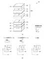
図4(b)は、他の実施の形態に用いられる第1の磁気抵抗素子100Bを例示する模式的斜視図である。図4(b)に表したように、第1の磁気抵抗素子100Bは、順に並べられた、下部電極E1と、下地層104と、第1磁性層101と、中間層103と、第2磁性層102と、磁気結合層107と、第2磁化固定層106と、ピニング層105と、キャップ層108と、上部電極E2とを含む。  FIG. 4B is a schematic perspective view illustrating the firstmagnetoresistive element 100B used in another embodiment. As shown in FIG. 4B, the firstmagnetoresistive element 100B includes a lower electrode E1, anunderlayer 104, a firstmagnetic layer 101, anintermediate layer 103, and a second magnetic element arranged in order. Thelayer 102, themagnetic coupling layer 107, the second magnetization fixedlayer 106, the pinninglayer 105, thecap layer 108, and the upper electrode E2 are included.

この例では、第1磁性層101は磁化自由層として機能し、第2磁性層102は第1磁化固定層として機能する。図4(b)の第1の磁気抵抗素子100Bは、トップスピンバルブ型と呼ばれる。第1の磁気抵抗素子100Bに含まれる層のそれぞれには、例えば、図4(a)に示す磁気抵抗素子に関して説明した材料を用いることができる。  In this example, the firstmagnetic layer 101 functions as a magnetization free layer, and the secondmagnetic layer 102 functions as a first magnetization fixed layer. The firstmagnetoresistive element 100B in FIG. 4B is called a top spin valve type. For each of the layers included in the firstmagnetoresistive element 100B, for example, the materials described for the magnetoresistive element shown in FIG.

図4(c)は、他の実施の形態に用いられる第1の磁気抵抗素子100Cを例示する模式的斜視図である。図4(c)に表したように、第1の磁気抵抗素子100Cは、順に並べられた、下部電極E1と、下地層104と、下部ピニング層105aと、下部第2磁化固定層106aと、下部磁気結合層107aと、下部第2磁性層102aと、下部中間層103aと、第1磁性層101と、上部中間層103bと、上部第2磁性層102bと、上部磁気結合層107bと、上部第2磁化固定層106bと、上部ピニング層105bと、キャップ層108と、上部電極E2とを含む。  FIG. 4C is a schematic perspective view illustrating the firstmagnetoresistive element 100C used in another embodiment. As shown in FIG. 4C, the firstmagnetoresistive element 100C includes a lower electrode E1, anunderlayer 104, a lower pinninglayer 105a, a lower second magnetization fixedlayer 106a, Lowermagnetic coupling layer 107a, lower secondmagnetic layer 102a, lowerintermediate layer 103a, firstmagnetic layer 101, upperintermediate layer 103b, upper secondmagnetic layer 102b, uppermagnetic coupling layer 107b, upper The second magnetization fixedlayer 106b, the upper pinninglayer 105b, thecap layer 108, and the upper electrode E2 are included.

この例では、第1磁性層101が磁化自由層として機能し、下部第2磁性層102aが下部第1磁化固定層102aとして機能し、上部第2磁性層102bが上部第1磁化固定層として機能する。既に説明した図4(a)に示す第1の磁気抵抗素子100A及び図4(b)に示す第1の磁気抵抗素子100Bにおいては、磁化自由層である第1磁性層101の一方の面側に磁化固定層である第2磁性層102が配置されている。一方、図4(c)に示す第1の磁気抵抗素子100Cにおいては、2つの磁化固定層の間に磁化自由層が配置されている。図4(c)に示す第1の磁気抵抗素子100Cは、デュアルスピンバルブ型と呼ばれる。図4(c)に示す第1の磁気抵抗素子100Cに含まれる層のそれぞれには、例えば、図4(a)に示す第1の磁気抵抗素子100Aに関して説明した材料を用いることができる。  In this example, the firstmagnetic layer 101 functions as a magnetization free layer, the lower secondmagnetic layer 102a functions as a lower first magnetization fixedlayer 102a, and the upper secondmagnetic layer 102b functions as an upper first magnetization fixed layer. To do. In the already described firstmagnetoresistive element 100A shown in FIG. 4A and the firstmagnetoresistive element 100B shown in FIG. 4B, one surface side of the firstmagnetic layer 101 which is a magnetization free layer is provided. The secondmagnetic layer 102, which is a magnetization fixed layer, is disposed. On the other hand, in the firstmagnetoresistive element 100C shown in FIG. 4C, a magnetization free layer is disposed between two magnetization fixed layers. The firstmagnetoresistive element 100C shown in FIG. 4C is called a dual spin valve type. For each of the layers included in the firstmagnetoresistive element 100C shown in FIG. 4C, for example, the materials described for the firstmagnetoresistive element 100A shown in FIG. 4A can be used.

図4(d)は、他の実施の形態に用いられる第1の磁気抵抗素子100Dを例示する模式的斜視図である。図4(d)に表したように、第1の磁気抵抗素子100Dは、順に並べられた、下部電極E1と、下地層104と、ピニング層105と、第2磁性層102と、中間層103と、第1磁性層101と、キャップ層108と、上部電極E2とを含む。  FIG. 4D is a schematic perspective view illustrating afirst magnetoresistance element 100D used in another embodiment. As shown in FIG. 4D, thefirst magnetoresistive element 100D includes the lower electrode E1, theunderlayer 104, the pinninglayer 105, the secondmagnetic layer 102, and theintermediate layer 103, which are arranged in order. A firstmagnetic layer 101, acap layer 108, and an upper electrode E2.

この例では、第1磁性層101は磁化自由層として機能し、第2磁性層102は磁化固定層として機能する。既に説明した図4(a)に示す第1の磁気抵抗素子100A及び図4(b)に示す第1の磁気抵抗素子100Bにおいては、第2磁化固定層106と、磁気結合層107と、第1磁化固定層として機能する第2磁性層102とを用いた構造が適用されている。一方、図4(d)に示す第1の磁気抵抗素子100Dにおいては、単一の磁化固定層24を用いたシングルピン構造が適用されている。図4(d)に示す第1の磁気抵抗素子100Dに含まれる層のそれぞれには、例えば、図4(a)に示す第1の磁気抵抗素子100Aに関して説明した材料を用いることができる。  In this example, the firstmagnetic layer 101 functions as a magnetization free layer, and the secondmagnetic layer 102 functions as a magnetization fixed layer. In the firstmagnetoresistive element 100A shown in FIG. 4A and the firstmagnetoresistive element 100B shown in FIG. 4B, the second magnetization fixedlayer 106, themagnetic coupling layer 107, the first A structure using the secondmagnetic layer 102 functioning as a single magnetization fixed layer is applied. On the other hand, in thefirst magnetoresistive element 100D shown in FIG. 4D, a single pin structure using a single magnetization fixed layer 24 is applied. For each of the layers included in thefirst magnetoresistive element 100D shown in FIG. 4D, for example, the materials described with respect to the firstmagnetoresistive element 100A shown in FIG. 4A can be used.

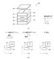
図5は、他の構成に係る第1の磁気抵抗素子100Eを例示する模式的斜視図である。図5に表したように、第1の磁気抵抗素子100Eにおいては、絶縁層109が設けられる。すなわち、下部電極E1と上部電極E2との間に、互いに離間する2つの絶縁層(絶縁部分)109が設けられ、それらの間に、下地層104と、ピニング層105と、第2磁化固定層106と、磁気結合層107と、第2磁性層102と、中間層103と、磁化自由層101と、キャップ層108からなる積層体が設けられる。  FIG. 5 is a schematic perspective view illustrating thefirst magnetoresistance element 100E according to another configuration. As shown in FIG. 5, the insulatinglayer 109 is provided in thefirst magnetoresistive element 100E. That is, two insulating layers (insulating portions) 109 that are separated from each other are provided between the lower electrode E1 and the upper electrode E2, and thebase layer 104, the pinninglayer 105, and the second magnetization fixed layer are provided therebetween. A laminated body including 106, amagnetic coupling layer 107, a secondmagnetic layer 102, anintermediate layer 103, a magnetizationfree layer 101, and acap layer 108 is provided.

この例では、第1磁性層101は磁化自由層として機能し、第2磁性層102は第1磁化固定層として機能する。第1の磁気抵抗素子100Eに含まれる層のそれぞれには、例えば、図4(a)に示す磁気抵抗素子に関して説明した材料を用いることができる。また、絶縁層109には、例えば、アルミニウム酸化物(例えば、Al)、または、シリコン酸化物(例えば、SiO)などを用いることができる。絶縁層109により、上記積層体の周囲におけるリーク電流を抑制することができる。上記の絶縁層109は、図4(a)〜(d)に示すいずれの磁気抵抗素子にも適用できる。In this example, the firstmagnetic layer 101 functions as a magnetization free layer, and the secondmagnetic layer 102 functions as a first magnetization fixed layer. For each of the layers included in thefirst magnetoresistive element 100E, for example, the materials described for the magnetoresistive element shown in FIG. For the insulatinglayer 109, for example, aluminum oxide (eg, Al2 O3 ), silicon oxide (eg, SiO2 ), or the like can be used. The insulatinglayer 109 can suppress leakage current around the stacked body. The insulatinglayer 109 can be applied to any of the magnetoresistive elements shown in FIGS.

[1−4.磁気抵抗素子の他の構成例]
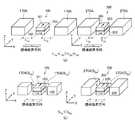
図6(a)は、他の構成に係る第1の磁気抵抗素子100Fを示す模式的斜視図である。図6(a)に示す第1の磁気抵抗素子100Fはグラニュラー型の磁気抵抗素子と呼ばれ、母層(マトリックス)中に磁性体の微粒子が3次元的に分散した構造と、この構造の側部に設けられる一対の電極Eとを有する。母層が導電体の場合にはグラニュラー型GMR素子と呼ばれ、絶縁体の場合にはグラニュラー型TMR素子と呼ばれる。
[1-4. Other configuration examples of magnetoresistive element]
FIG. 6A is a schematic perspective view showing a firstmagnetoresistive element 100F according to another configuration. The firstmagnetoresistive element 100F shown in FIG. 6A is called a granular type magnetoresistive element, and has a structure in which fine particles of magnetic material are three-dimensionally dispersed in a mother layer (matrix), and a side of this structure. And a pair of electrodes E provided in the part. When the mother layer is a conductor, it is called a granular type GMR element, and when it is an insulator, it is called a granular type TMR element.

図6(c)に示すとおり、外部磁界なしの状態では、3次元的に分散した磁性粒子の磁化の向きは3次元的にランダムとなっており、図6(b)、(d)に示すとおり、外部磁界が加わると一方向に揃う。図6(e)に示したとおり、分散した磁性粒子の相対角度に応じて電気抵抗が変化する。このMR現象は、前述した積層型のGMR素子やTMR素子と同じ原理に基づく。第1の磁気抵抗素子100Fは、積層型に比べて作製が容易であるなどの利点を持つ。  As shown in FIG. 6C, in the state without an external magnetic field, the magnetization directions of the magnetic particles dispersed three-dimensionally are random three-dimensionally, as shown in FIGS. 6B and 6D. As shown, when an external magnetic field is applied, they are aligned in one direction. As shown in FIG. 6E, the electric resistance changes according to the relative angle of the dispersed magnetic particles. This MR phenomenon is based on the same principle as the above-described stacked GMR element and TMR element. The firstmagnetoresistive element 100F has advantages such as being easier to manufacture than the stacked type.

第1の磁気抵抗素子100Fに用いられる磁性粒子は、前述した積層型の磁気抵抗素子における磁化自由層に対応する。磁性粒子に用いられる材料として、例えば、Fe、Co及びNiの少なくともいずれか、または、これらの少なくとも1種を含む合金とすることができる。また、これらの金属、合金に、添加元素として、B,Al,Si,Mg,C,Ti,V,Cr,Mn、Cu,Zn,Ga,Zr,Hfなどを添加することもできる。例えば、Co90Fe10からなる磁性粒子を用いることができる。The magnetic particles used in the firstmagnetoresistive element 100F correspond to the magnetization free layer in the multilayer magnetoresistive element described above. As a material used for the magnetic particles, for example, at least one of Fe, Co, and Ni, or an alloy containing at least one of them can be used. Further, B, Al, Si, Mg, C, Ti, V, Cr, Mn, Cu, Zn, Ga, Zr, Hf, and the like can be added to these metals and alloys as additive elements. For example, magnetic particles made of Co90 Fe10 can be used.

第1の磁気抵抗素子100Fのマトリックスとしては、グラニュラー型TMR素子の場合には、絶縁材料や半導体材料として、マグネシウム酸化物(Mg−O等)、アルミ酸化物(Al等)、チタン酸化物(Ti−O等)、亜鉛酸化物(Zn−O等)、または、酸化ガリウム(Ga−O)などが用いられる。一方、グラニュラー型GMR素子の場合には、導電体材料として、Cu,Ag,Au,Al,Cr,Ruなどの金属を用いることができる。As a matrix of the firstmagnetoresistive element 100F, in the case of a granular type TMR element, as an insulating material or a semiconductor material, magnesium oxide (Mg—O or the like), aluminum oxide (Al2 O3 or the like), titanium An oxide (Ti—O or the like), zinc oxide (Zn—O or the like), gallium oxide (Ga—O), or the like is used. On the other hand, in the case of a granular type GMR element, a metal such as Cu, Ag, Au, Al, Cr, Ru can be used as the conductor material.

尚、第1の磁気抵抗素子100Fは、電極Eを側壁に設け、膜面内方向に通電するCIP素子として形成されているが、下部電極E1及び上部電極E2を介して膜面垂直方向に通電を行うCPP素子とすることもできる。  The firstmagnetoresistive element 100F is formed as a CIP element in which the electrode E is provided on the side wall and energizes in the in-plane direction of the film. It is also possible to use a CPP element that performs the above.

[1−5.磁気抵抗素子の磁場感度の調整]
次に、磁気抵抗素子の磁場感度の調整について説明する。磁気抵抗素子の磁場感度を調整するためには、線形応答磁性体を用いる方法、磁束ガイドを用いる方法、磁気抵抗素子の配置による方法及びその他の方法を適用することが可能である。線形応答磁性体は、被測定電流による誘導磁界の方向と略垂直な方向から磁気抵抗素子に磁場を印加する。本実施の形態に係る電流センサは、この線形応答磁性体を用いて磁場感度の調整を行っている。
[1-5. Adjustment of magnetic field sensitivity of magnetoresistive element]
Next, adjustment of the magnetic field sensitivity of the magnetoresistive element will be described. In order to adjust the magnetic field sensitivity of the magnetoresistive element, it is possible to apply a method using a linear response magnetic body, a method using a magnetic flux guide, a method using an arrangement of magnetoresistive elements, and other methods. The linear response magnetic body applies a magnetic field to the magnetoresistive element from a direction substantially perpendicular to the direction of the induced magnetic field caused by the current to be measured. The current sensor according to the present embodiment uses this linear response magnetic body to adjust the magnetic field sensitivity.

[1−6.横置き線形応答磁性体]
線形応答磁性体を用いて磁気抵抗素子の磁場感度を調整する方法について説明する。図7は、第1の磁気抵抗素子100と、第1の線形応答磁性体160Aの模式図である。第1の線形応答磁性体160Aは、線形応答磁性体の一態様である。
[1-6. Horizontally mounted linear response magnetic body]
A method for adjusting the magnetic field sensitivity of the magnetoresistive element using the linear response magnetic material will be described. FIG. 7 is a schematic diagram of the firstmagnetoresistive element 100 and the first linear responsemagnetic body 160A. The first linear responsemagnetic body 160A is an embodiment of the linear response magnetic body.

第1の線形応答磁性体160Aは、第1の磁気抵抗素子100中の第1磁性層101、第2磁性層102及び中間層103に隣接して配置され、第1磁性層101、第2磁性層102及び中間層103に磁界を加える。また、第1の線形応答磁性体160Aは、下部電極E1と上部電極E2との間に設けられる。更に、例えば第1の線形応答磁性体160Aと第1の磁気抵抗素子100との間には、絶縁層109が配置される。この例では、第1の線形応答磁性体160Aと下部電極E1との間に、絶縁層109が延在している。  The first linear responsemagnetic body 160A is disposed adjacent to the firstmagnetic layer 101, the secondmagnetic layer 102, and theintermediate layer 103 in the firstmagnetoresistive element 100, and the firstmagnetic layer 101, the second magnetic layer A magnetic field is applied to thelayer 102 and theintermediate layer 103. The first linear responsemagnetic body 160A is provided between the lower electrode E1 and the upper electrode E2. Further, for example, the insulatinglayer 109 is disposed between the first linear responsemagnetic body 160 </ b> A and the firstmagnetoresistive element 100. In this example, the insulatinglayer 109 extends between the first linear responsemagnetic body 160A and the lower electrode E1.

図7では1つの第1の磁気抵抗素子100を挟むように一対の第1の線形応答磁性体160Aが設けられる。しかし、1つの第1の磁気抵抗素子100に対して1つの第1の線形応答磁性体160Aを設けてもよい。以降で説明する具体例においても1対の第1の線形応答磁性体160Aが設けられているが、片側のみとしてもよい。  In FIG. 7, a pair of first linear responsemagnetic bodies 160 </ b> A are provided so as to sandwich onefirst magnetoresistive element 100. However, one first linear responsemagnetic body 160A may be provided for onefirst magnetoresistive element 100. Also in the specific examples described below, the pair of first linear responsemagnetic bodies 160A is provided, but only one side may be provided.

第1の線形応答磁性体160Aの磁界により、外部磁界が印加されていない状態における第1の磁性層101の磁化方向を所望の方向に設定できる。例えば、第1の線形応答磁性体160Aの磁化方向を第2の磁性層102の磁化方向と直交方向に設定することで、図3(b)に示すように、第1の磁性層101の磁化方向を第2の磁性層102の磁化方向と直交させることができる。第1の磁性層101の磁化方向と第2の磁性層102の磁化方向とを交差(直交)させることで、図3(d)に示すように正負の磁界に線形的に感応させることができる。  With the magnetic field of the first linear responsemagnetic body 160A, the magnetization direction of the firstmagnetic layer 101 in a state where no external magnetic field is applied can be set to a desired direction. For example, by setting the magnetization direction of the first linear responsemagnetic body 160A to a direction orthogonal to the magnetization direction of the secondmagnetic layer 102, as shown in FIG. 3B, the magnetization of the firstmagnetic layer 101 The direction can be orthogonal to the magnetization direction of the secondmagnetic layer 102. By making the magnetization direction of the firstmagnetic layer 101 and the magnetization direction of the secondmagnetic layer 102 intersect (orthogonal), it is possible to linearly respond to positive and negative magnetic fields as shown in FIG. .

第1の線形応答磁性体160Aには、例えば、Co−Pt、Fe−Pt、Co−Pd、Fe−Pdなどの磁気異方性および保磁力が比較的高いハード磁性材料(硬質強磁性材料)が用いられる。また、Co−Pt、Fe−Pt、Co−Pd、Fe−Pdにさらに添加元素を加えた合金を用いても良い。例えば、CoPt(Coの比率は、50at.%以上85at.%以下)、(CoPt100−x100−yCr(xは50at.%以上85at.%以下、yは0at.%以上40at.%以下)、または、FePt(Ptの比率は40at.%以上60at.%以下)などが用いられてもよい。このような材料を用いる場合、第1の線形応答磁性体160Aの磁化の方向は、線形応答磁性体160Aの保磁力よりも大きい外部磁界を加えることで、外部磁界を加えた方向に設定(固定)することができる。第1の線形応答磁性体160Aの厚さ(例えば、下部電極E1から上部電極E2に向かう方向に沿った長さ)は、例えば5nm以上50nm以下である。The first linear responsemagnetic body 160A includes, for example, a hard magnetic material (hard ferromagnetic material) having a relatively high magnetic anisotropy and coercive force, such as Co—Pt, Fe—Pt, Co—Pd, and Fe—Pd. Is used. Alternatively, an alloy obtained by further adding an additive element to Co—Pt, Fe—Pt, Co—Pd, or Fe—Pd may be used. For example, CoPt (ratio of Co is, 50at.% Or more 85 at.% Orless), (Co x Pt 100- x) 100-y Cr y (x is 50at.% Or more 85 at.% Or less, y is 0 atomic.% Or more 40 at.% Or less) or FePt (the ratio of Pt is 40 at.% To 60 at.%) May be used. When such a material is used, the direction of magnetization of the first linear responsemagnetic body 160A is set (fixed) by applying an external magnetic field larger than the coercive force of the linear responsemagnetic body 160A. )can do. The thickness (for example, the length along the direction from the lower electrode E1 to the upper electrode E2) of the first linear responsemagnetic body 160A is, for example, 5 nm or more and 50 nm or less.

図7に示すように、第1の線形応答磁性体160Aと下部電極E1との間に絶縁層109を配置する場合、絶縁層109の材料として、SiOやAlOを用いることができる。さらに、絶縁層109と第1の線形応答磁性体160Aの間に、図示しない磁性体下地層を設けてもよい。線形応答磁性体160AにCo−Pt、Fe−Pt、Co−Pd、Fe−Pdなどの磁気異方性および保磁力が比較的高い硬質強磁性材料を用いる場合には、磁性体下地層の材料として、CrやFe−Coなどを用いることができる。上記の第1の線形応答磁性体160Aは、上記及び以下で説明する第1の磁気抵抗素子100のいずれにも適用できる。As shown in FIG. 7, when the insulatinglayer 109 is disposed between the first linear responsemagnetic body 160A and the lower electrode E1, SiOx or AlOx can be used as the material of the insulatinglayer 109. Further, a magnetic underlayer (not shown) may be provided between the insulatinglayer 109 and the first linear responsemagnetic body 160A. When a hard ferromagnetic material having a relatively high magnetic anisotropy and coercive force such as Co—Pt, Fe—Pt, Co—Pd, and Fe—Pd is used for the linear responsemagnetic body 160A, the material of the magnetic underlayer For example, Cr or Fe—Co can be used. The first linear responsemagnetic body 160A can be applied to any of the firstmagnetoresistive elements 100 described above and below.

第1の線形応答磁性体160Aは、図示しない線形応答磁性体用ピニング層に積層された構造を有していてもよい。この場合、第1の線形応答磁性体160Aと線形応答磁性体用ピニング層の交換結合により、第1の線形応答磁性体160Aの磁化の方向を設定(固定)できる。この場合、第1の線形応答磁性体160Aには、Fe、Co及びNiの少なくともいずれか、または、これらの少なくとも1種を含む合金からなる強磁性材料を用いることができる。この場合、第1の線形応答磁性体160Aには、例えば、CoFe100−x合金(xは0at.%以上100at.%以下)、NiFe100−x合金(xは0at.%以上100at.%以下)、または、これらに非磁性元素を添加した材料が用いることができる。第1の線形応答磁性体160Aとして、前述した第2磁性層102と同様の材料を用いることができる。また、線形応答磁性体用ピニング層には、前述した磁気抵抗素子のピニング層105と同様の材料を用いることができる。また、線形応答磁性体用ピニング層を設ける場合、磁気抵抗素子の下地層で説明した材料と同様の下地層を線形応答磁性体用ピニング層の下に設けても良い。また、線形応答磁性体用ピニング層は、第1の線形応答磁性体160Aの下部に設けても良いし、上部に設けても良い。この場合の第1の線形応答磁性体160Aの磁化方向は、磁気抵抗素子のピニング層で説明したとおり、磁界中熱処理により決定することができる。160 A of 1st linear response magnetic bodies may have the structure laminated | stacked on the pinning layer for linear response magnetic bodies which is not shown in figure. In this case, the direction of magnetization of the first linear responsemagnetic body 160A can be set (fixed) by exchange coupling between the first linear responsemagnetic body 160A and the linear response magnetic body pinning layer. In this case, for the first linear responsemagnetic body 160A, a ferromagnetic material made of an alloy containing at least one of Fe, Co, and Ni, or at least one of them can be used. In this case, the first linear responsemagnetic body 160A includes, for example, a Cox Fe100-x alloy (x is 0 at.% Or more and 100 at.% Or less), a Nix Fe100-x alloy (x is 0 at.% Or more). 100 at.% Or less), or a material obtained by adding a nonmagnetic element to these can be used. As the first linear responsemagnetic body 160A, the same material as that of the secondmagnetic layer 102 described above can be used. The linear response magnetic pinning layer can be made of the same material as the pinninglayer 105 of the magnetoresistive element described above. When the linear response magnetic pinning layer is provided, an underlayer similar to the material described for the underlayer of the magnetoresistive element may be provided under the linear response magnetic pinning layer. Further, the linear response magnetic body pinning layer may be provided in the lower portion or the upper portion of the first linear responsemagnetic body 160A. In this case, the magnetization direction of the first linear responsemagnetic body 160A can be determined by heat treatment in a magnetic field as described in the pinning layer of the magnetoresistive element.

上記の第1の線形応答磁性体160Aは、上記第1の磁気抵抗素子100及び以下で説明する第1の磁気抵抗素子100のいずれにも適用できる。上述したような第1の線形応答磁性体160Aと線形応答磁性体用ピニング層の積層構造を用いた場合、被測定電流として瞬間的に大電流が流れ、大きい誘導磁界が第1の線形応答磁性体160Aに加わった場合においても、第1の線形応答磁性体160Aの磁化の向きを容易に保持することが出来る。  The first linear responsemagnetic body 160A can be applied to both the firstmagnetoresistive element 100 and the firstmagnetoresistive element 100 described below. When the laminated structure of the first linear responsemagnetic body 160A and the linear response magnetic body pinning layer as described above is used, a large current instantaneously flows as a current to be measured, and a large induced magnetic field is generated by the first linear response magnetic body. Even when added to thebody 160A, the magnetization direction of the first linear responsemagnetic body 160A can be easily maintained.

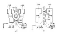
ここで、磁気抵抗素子の磁場感度((dR/R)/2Hs)は、線形応答磁性体等の構成によって調整することができる。図8(a)〜(c)には、2つの磁気抵抗素子について異なる磁場感度を得るために、第1の線形応答磁性体160A及び第2の線形応答磁性体260Aの構成に差を設けた例を示す。尚、図8(a)〜(c)においては、電流センサが2つの磁気抵抗素子を備える例について説明しているが、電流センサは、当然3つ以上の磁気抵抗素子を備えていても良い。また、図8では、図7に示すような、磁気抵抗素子の側方に隣接して第1又は第2の線形応答磁性体160A,260Aを設けた場合を例にとり説明しているが、磁気抵抗素子の斜め側方に第1又は第2の線形応答磁性体を設けた場合でも、同様に異なる磁場感度を得ることができる。尚、図8及び以下の図中において、201は第2の磁気抵抗素子200の第1磁性層(磁化自由層)を、202は中間層を、203は第2磁性層(磁化固定層)を、それぞれ表している。  Here, the magnetic field sensitivity ((dR / R) / 2Hs) of the magnetoresistive element can be adjusted by the configuration of a linear response magnetic body or the like. 8A to 8C, in order to obtain different magnetic field sensitivities for the two magnetoresistive elements, a difference is provided in the configuration of the first linear responsemagnetic body 160A and the second linear responsemagnetic body 260A. An example is shown. 8A to 8C, an example in which the current sensor includes two magnetoresistive elements has been described. However, the current sensor may naturally include three or more magnetoresistive elements. . FIG. 8 shows an example in which the first or second linear responsemagnetic bodies 160A and 260A are provided adjacent to the side of the magnetoresistive element as shown in FIG. Even when the first or second linear response magnetic body is provided on the oblique side of the resistance element, different magnetic field sensitivities can be obtained similarly. 8 and the following drawings, 201 is the first magnetic layer (magnetization free layer) of thesecond magnetoresistive element 200, 202 is the intermediate layer, and 203 is the second magnetic layer (magnetization fixed layer). , Respectively.

図8(a)に示すとおり、磁気抵抗素子と第1及び第2の線形応答磁性体160A,260Aとの間の距離を変えることで、磁場感度を変えることが可能である。図8(a)に示す第1の磁気抵抗素子100と一対の第1の線形応答磁性体160Aとのそれぞれの間の距離の和L1a+L1bは、第2の磁気抵抗素子200と一対の第2の線形応答磁性体260Aのそれぞれの距離の和L2a+L2bよりも大きく設定されている。この場合、第1又は第2の線形応答磁性体160A,260Aから距離が大きいほど、第1又は第2の磁気抵抗素子100,200に加わる磁界は小さくなる。従って、第1の磁気抵抗素子100の飽和磁場Hsは小さくなり、第1の磁気抵抗素子100の磁場感度((dR/R)/2Hs)は、第2の磁気抵抗素子200と比較して高く設定される。As shown in FIG. 8A, the magnetic field sensitivity can be changed by changing the distance between the magnetoresistive element and the first and second linear responsemagnetic bodies 160A and 260A. The sum L1a + L1b of the distance between each of the firstmagnetoresistive element 100 and the pair of first linear responsemagnetic bodies 160A shown in FIG. It is set larger than the sum L2a + L2b of the distances of the second linear responsemagnetic body 260A. In this case, the greater the distance from the first or second linear responsemagnetic body 160A, 260A, the smaller the magnetic field applied to the first or secondmagnetoresistive element 100, 200. Therefore, the saturation magnetic field Hs of the firstmagnetoresistive element 100 is reduced, and the magnetic field sensitivity ((dR / R) / 2Hs) of the firstmagnetoresistive element 100 is higher than that of thesecond magnetoresistive element 200. Is set.

図8(b)に示すとおり、第1の線形応答磁性体160Aの基板平面における面積と、第2の線形応答磁性体260Aの基板平面における面積を変えることで、磁場感度を変えることが可能である。図8(b)に示す一対の第1の線形応答磁性体160Aのそれぞれの面積の和S1a+S1bは、一対の第2の線形応答磁性体260Aのそれぞれの面積の和S2a+S2bよりも小さく設定されている。この場合、第1又は第2の線形応答磁性体160A,260Aの面積が大きいほど、第1又は第2の線形応答磁性体160A,260Aの磁気体積が大きくなる。従って、第1の磁気抵抗素子100の飽和磁場Hsは小さくなり、第1の磁気抵抗素子100の磁場感度((dR/R)/2Hs)は、第2の磁気抵抗素子200と比較して高く設定される。As shown in FIG. 8B, the magnetic field sensitivity can be changed by changing the area of the first linear responsemagnetic body 160A on the substrate plane and the area of the second linear responsemagnetic body 260A on the substrate plane. is there. The area sum S1a + S1b of each of the pair of first linear responsemagnetic bodies 160A illustrated in FIG. 8B is greater than the area sum S2a + S2b of each of the pair of second linear responsemagnetic bodies 260A. Is set too small. In this case, the larger the area of the first or second linear responsemagnetic body 160A, 260A, the larger the magnetic volume of the first or second linear responsemagnetic body 160A, 260A. Therefore, the saturation magnetic field Hs of the firstmagnetoresistive element 100 is reduced, and the magnetic field sensitivity ((dR / R) / 2Hs) of the firstmagnetoresistive element 100 is higher than that of thesecond magnetoresistive element 200. Is set.

図8(c)に示すとおり、第1及び第2の線形応答磁性体160A,260Aの膜厚を変えることで、磁場感度を変えることが可能である。図8(c)に示す一対の第1の線形応答磁性体160Aのそれぞれの膜厚の和t1a+t1bは、一対の第2の線形応答磁性体260Aのそれぞれの膜厚の和t2a+t2bよりも小さく設定されている。この場合、第1及び第2の線形応答磁性体160A,260Aの膜厚が厚いほど、第1及び第2の線形応答磁性体160A,260Aの磁気体積が大きくなる。従って、第1の磁気抵抗素子100の飽和磁場Hsは小さくなり、第1の磁気抵抗素子100の磁場感度((dR/R)/2Hs)は、第2の磁気抵抗素子200と比較して高く設定される。As shown in FIG. 8C, the magnetic field sensitivity can be changed by changing the film thickness of the first and second linear responsemagnetic bodies 160A and 260A. The sum of film thicknesses t1a + t1b of the pair of first linear responsemagnetic bodies 160A shown in FIG. 8C is the sum of film thicknesses of the pair of second linear responsemagnetic bodies 260A t2a + t. It is set smaller than2b . In this case, the larger the film thickness of the first and second linear responsemagnetic bodies 160A and 260A, the larger the magnetic volume of the first and second linear responsemagnetic bodies 160A and 260A. Therefore, the saturation magnetic field Hs of the firstmagnetoresistive element 100 is reduced, and the magnetic field sensitivity ((dR / R) / 2Hs) of the firstmagnetoresistive element 100 is higher than that of thesecond magnetoresistive element 200. Is set.

上述した図8(b)、図8(c)では、第1及び第2の線形応答磁性体160A,260Aの面積または膜厚を変えることで磁気体積を変えた場合について説明したが、第1及び第2の線形応答磁性体160A,260Aに用いられる磁性材料の種類を変えることでも磁気体積を変えることができる。例えば、第1の線形応答磁性体160Aと第2の線形応答磁性体260Aのそれぞれに飽和磁化の異なる磁性材料を用いることで、磁気体積を変え、第1および第2の磁気抵抗素子100,200の磁場感度を変えることも出来る。  In FIGS. 8B and 8C described above, the case where the magnetic volume is changed by changing the area or film thickness of the first and second linear responsemagnetic bodies 160A and 260A has been described. The magnetic volume can also be changed by changing the type of magnetic material used for the second linear responsemagnetic bodies 160A and 260A. For example, by using magnetic materials having different saturation magnetizations for the first linear responsemagnetic body 160A and the second linear responsemagnetic body 260A, the magnetic volume is changed, and the first andsecond magnetoresistance elements 100, 200 are changed. You can change the magnetic field sensitivity.

図9(a)及び(b)には、複数の磁気抵抗素子に対して、一対の第1の線形応答磁性体160D又は160Eから磁界を印加する場合について説明するための模式図である。第1の線形応答磁性体160D又は160Eは、第1の線形応答磁性体160の他の態様である。このような構成によっても、それぞれの磁気抵抗素子の磁場感度を変えることが可能である。尚、図9においては、電流センサが第1の磁気抵抗素子100及び第2の磁気抵抗素子200に加え、第3の磁気抵抗素子300を備えた例について説明する。但し、磁気抵抗素子の数は2つでも良いし、4つ以上でも良い。  FIGS. 9A and 9B are schematic diagrams for explaining a case where a magnetic field is applied from a pair of first linear responsemagnetic bodies 160D or 160E to a plurality of magnetoresistive elements. The first linear responsemagnetic body 160D or 160E is another embodiment of the first linear responsemagnetic body 160. Even with such a configuration, it is possible to change the magnetic field sensitivity of each magnetoresistive element. In FIG. 9, an example in which the current sensor includes a thirdmagnetoresistive element 300 in addition to the firstmagnetoresistive element 100 and thesecond magnetoresistive element 200 will be described. However, the number of magnetoresistive elements may be two, or four or more.

図9(a)に示すとおり、複数の磁気抵抗素子に対して、一対の第1の線形応答磁性体160Dを用いても、それぞれの磁気抵抗素子の磁場感度を変えることが可能である。図9(a)では、第1の線形応答磁性体160Dの磁化方向(Y方向)における幅がそれぞれの磁気抵抗素子に対して同等となっているが、複数の磁気抵抗素子のそれぞれと一対の第1の線形応答磁性体160Dの間の距離が異なる。このような形状の第1の線形応答磁性体160Dを用いることによって、それぞれの磁気抵抗素子に最も近接した位置の第1の線形応答磁性体160Dとそれぞれの磁気抵抗素子の間の実効的な距離が異なるため、図8(a)で説明したとおり、それぞれの磁気抵抗素子の磁場感度を変えることが可能となる。  As shown in FIG. 9A, even if a pair of first linear responsemagnetic bodies 160D is used for a plurality of magnetoresistive elements, the magnetic field sensitivity of each magnetoresistive element can be changed. In FIG. 9A, the width in the magnetization direction (Y direction) of the first linear responsemagnetic body 160D is equal to each magnetoresistive element. The distance between the first linear responsemagnetic bodies 160D is different. By using the first linear responsemagnetic body 160D having such a shape, an effective distance between the first linear responsemagnetic body 160D closest to each magnetoresistive element and each magnetoresistive element. Therefore, as described in FIG. 8A, the magnetic field sensitivity of each magnetoresistive element can be changed.

図9(b)に示すとおり、複数の磁気抵抗素子に対して、一対の第1の線形応答磁性体160Eを用いても、それぞれの磁気抵抗素子の磁場感度を変えることが可能である。図9(b)では、第1の線形応答磁性体160Eの磁化方向(Y方向)における幅がそれぞれの磁気抵抗素子に対して異なっており、かつ、複数の磁気抵抗素子のそれぞれと一対の第1の線形応答磁性体160Eの間の距離が異なる。このような形状の第1の線形応答磁性体160Eを用いた場合、それぞれの磁気抵抗素子に最も近接した位置の第1の線形応答磁性体160Eとそれぞれの磁気抵抗素子の間の実効的な距離および面積が異なるため、図8(a)、(b)で説明したとおり、それぞれの磁気抵抗素子の磁場感度を変えることが可能となる。  As shown in FIG. 9B, even if a pair of first linear responsemagnetic bodies 160E is used for a plurality of magnetoresistive elements, the magnetic field sensitivity of each magnetoresistive element can be changed. In FIG. 9B, the width in the magnetization direction (Y direction) of the first linear responsemagnetic body 160E is different for each magnetoresistive element, and each of the plurality of magnetoresistive elements is paired with the pair of first magnetoresistive elements. The distances between the one linear responsemagnetic bodies 160E are different. When the first linear responsemagnetic body 160E having such a shape is used, an effective distance between the first linear responsemagnetic body 160E closest to each magnetoresistive element and each magnetoresistive element. Since the areas are different, the magnetic field sensitivity of each magnetoresistive element can be changed as described with reference to FIGS.

ここまで説明した線形応答磁性体160A〜Eのいずれにおいても、Co−Pt、Fe−Pt、Co−Pd、Fe−Pdなどの磁気異方性および保磁力が比較的高い硬質強磁性材料を用いることができ、また、線形応答磁性体と線形応答磁性体用ピニング層とを積層した構造を用いてもよい。図10には、図8(a)のバリエーションとして、それぞれ第1の線形応答磁性体160A及び第2の線形応答磁性体260Aの下面に接する線形応答磁性体用ピニング層169及び269を配置した例を示す。ピニング層169及び269は、線形応答磁性体用ピニング層の一例である。尚、図10においては図8(a)の変形例を示しているが、このような線形応答磁性体と線形応答磁性体用のピニング層を用いたバリエーションは、図7〜図9のいずれの例にも適用できる。また、線形応答磁性体用ピニング層は、線形応答磁性体の下部に設けても良いし、上部に設けても良い。  Any of the linear responsemagnetic bodies 160A to 160E described so far uses a hard ferromagnetic material having a relatively high magnetic anisotropy and coercive force, such as Co—Pt, Fe—Pt, Co—Pd, and Fe—Pd. Alternatively, a structure in which a linear response magnetic body and a linear response magnetic pinning layer are stacked may be used. FIG. 10 shows an example in which linear response magnetic pinninglayers 169 and 269 are arranged in contact with the lower surfaces of the first linear responsemagnetic body 160A and the second linear responsemagnetic body 260A, respectively, as a variation of FIG. 8A. Indicates. The pinninglayers 169 and 269 are examples of a linear response magnetic pinning layer. FIG. 10 shows a modification of FIG. 8A. Variations using such a linear response magnetic body and a pinning layer for the linear response magnetic body are shown in any of FIGS. It can also be applied to examples. Further, the linear response magnetic body pinning layer may be provided at the lower portion or the upper portion of the linear response magnetic body.

図11は、第1の線形応答磁性体160Aと線形応答磁性体用ピニング層169の積層の構成例を示す模式図である。第1の線形応答磁性体160Aと線形応答磁性体用ピニング層169の積層構造を用いる場合、図11(a)に示す構造だけでなく、図11(b)に示すように、線形応答磁性体用ピニング層169/線形応答磁性体160A/線形応答磁性体用磁気結合層169/線形応答磁性体160Aのような積層構造としてもよい。また、図11(c)に示すように、線形応答磁性体用磁気結合層168を介して線形応答磁性体160Aを3層以上積層してもよい。このような積層構造の場合、線形応答磁性体用磁気結合層169を介した2つの線形応答磁性体160Aは互いに反平行の磁化方向となる。この場合、第1の磁気抵抗素子100の第1磁性層101に最も距離の近い第1の線形応答磁性体160Aの磁化の向きに第1磁性層101の磁化が向く。また、このような構造を用いる場合、第1の磁気抵抗素子100の第1磁性層101に最も距離の近い線形応答磁性体160Aの厚みを、積層構造に含まれるほかの線形応答磁性体160Aの厚みよりも厚くすることが好ましい。  FIG. 11 is a schematic diagram illustrating a configuration example of a stack of the first linear responsemagnetic body 160A and the linear response magneticbody pinning layer 169. When the laminated structure of the first linear responsemagnetic body 160A and the linear response magneticbody pinning layer 169 is used, not only the structure shown in FIG. 11A but also the linear response magnetic body shown in FIG. A laminated structure such as a pinninglayer 169 / linear responsemagnetic body 160A /magnetic coupling layer 169 for linear response magnetic body / linear responsemagnetic body 160A may be used. Further, as shown in FIG. 11C, three or more linear responsemagnetic bodies 160A may be stacked via the linear response magnetic bodymagnetic coupling layer 168. In the case of such a laminated structure, the two linear responsemagnetic bodies 160A via the linear response magnetic bodymagnetic coupling layer 169 have antiparallel magnetization directions. In this case, the magnetization of the firstmagnetic layer 101 is oriented in the direction of the magnetization of the first linear responsemagnetic body 160 </ b> A that is closest to the firstmagnetic layer 101 of the firstmagnetoresistive element 100. When such a structure is used, the thickness of the linear responsemagnetic body 160A closest to the firstmagnetic layer 101 of the firstmagnetoresistive element 100 is set to the thickness of the other linear responsemagnetic body 160A included in the stacked structure. It is preferable to make it thicker than the thickness.

第1の線形応答磁性体160Aと線形応答磁性体用ピニング層169の積層構造を用いた場合、被測定電流として瞬間的に大電流が流れ、大きい誘導磁界が第1の線形応答磁性体160Aに加わった場合においても、第1の線形応答磁性体160Aの磁化の向きを容易に保持することが出来る。  When the laminated structure of the first linear responsemagnetic body 160A and the linear response magneticbody pinning layer 169 is used, a large current instantaneously flows as a current to be measured, and a large induced magnetic field flows into the first linear responsemagnetic body 160A. Even when added, the magnetization direction of the first linear responsemagnetic body 160A can be easily maintained.

[1−7.縦置き線形応答磁性体]
次に、線形応答磁性体を磁気抵抗素子に積層して配置する場合の磁気抵抗素子と線形応答磁性体との関係について説明する。以下の説明においては、第1の磁気抵抗素子100と第1の線形応答磁性体160を例として説明するが第2の磁気抵抗素子200や第2の線形応答磁性体260等も同様に構成することが可能である。
[1-7. Vertically mounted linear response magnetic body]
Next, the relationship between the magnetoresistive element and the linear response magnetic body when the linear response magnetic body is laminated on the magnetoresistive element will be described. In the following description, the firstmagnetoresistive element 100 and the first linear responsemagnetic body 160 will be described as an example. However, thesecond magnetoresistive element 200, the second linear response magnetic body 260, and the like are configured similarly. It is possible.

図12には、第1の磁気抵抗素子100と、線形応答磁性体として機能する第1の線形応答磁性体160Fの模式図を示す。第1の線形応答磁性体160Fは、第1の線形応答磁性体160の他の態様である。尚、図12においては、上部電極E2を省略している。  FIG. 12 is a schematic diagram of the firstmagnetoresistive element 100 and the first linear responsemagnetic body 160F that functions as a linear response magnetic body. The first linear responsemagnetic body 160F is another embodiment of the first linear responsemagnetic body 160. In FIG. 12, the upper electrode E2 is omitted.

本実施の形態においては、第1の線形応答磁性体160Fが第1の磁気抵抗素子100の積層方向に設けられる。例えば、第1の線形応答磁性体160Fは、図12に示すように、第1の磁気抵抗素子100中のキャップ層108の上に設けられる。但し、第1の線形応答磁性体160Fは、例えば下地層104よりも下方に設けてもよい。但し、磁化自由層として機能する第1磁性層101が磁化固定層として機能する第2磁性層102よりも上に位置する場合には、第1磁性層101よりも上に第1の線形応答磁性体160Fを設けたほうが好ましく、第1磁性層101が第2磁性層102よりも下に位置する場合には、第2磁性層102よりも下に第1の線形応答磁性体160Fを設けたほうが好ましい。  In the present embodiment, the first linear responsemagnetic body 160F is provided in the stacking direction of the firstmagnetoresistive element 100. For example, the first linear responsemagnetic body 160F is provided on thecap layer 108 in the firstmagnetoresistive element 100 as shown in FIG. However, the first linear responsemagnetic body 160F may be provided below theunderlayer 104, for example. However, when the firstmagnetic layer 101 functioning as the magnetization free layer is positioned above the secondmagnetic layer 102 functioning as the magnetization fixed layer, the first linear response magnetism is positioned above the firstmagnetic layer 101. It is preferable to provide thebody 160F. When the firstmagnetic layer 101 is located below the secondmagnetic layer 102, it is preferable to provide the first linear responsemagnetic body 160F below the secondmagnetic layer 102. preferable.

また、図12に示すとおり、第1の線形応答磁性体とキャップ層108の間に第1の線形応答磁性体160F用の下地層161を設けてもよい。図12において、第1の線形応答磁性体160上に図示しない上部電極を設けることで、上部電極と下部電極E1の間に通電した電流が第1の線形応答磁性体160Fと磁気抵抗素子に流れる。また、上部電極は、第1の線形応答磁性体160Fとキャップ層108の間に設けても良い。  In addition, as shown in FIG. 12, anunderlayer 161 for the first linear responsemagnetic body 160F may be provided between the first linear response magnetic body and thecap layer 108. In FIG. 12, by providing an upper electrode (not shown) on the first linear responsemagnetic body 160, a current passed between the upper electrode and the lower electrode E1 flows through the first linear responsemagnetic body 160F and the magnetoresistive element. . The upper electrode may be provided between the first linear responsemagnetic body 160F and thecap layer 108.

第1の線形応答磁性体160Fを用いることにより、上述した第1の線形応答磁性体160Aを用いた場合と同様の効果を得ることが可能である。ここで、第1の線形応答磁性体160Fは第1の磁性層101等の積層方向に設けられる為、第1の線形応答磁性体160Fから第1の磁性層101への漏洩磁界は第1の線形応答磁性体160Fの磁化方向と逆向きとなる。尚、このような第1の線形応答磁性体160Fを前述した線形応答磁性体と組み合わせて使用してもよい。  By using the first linear responsemagnetic body 160F, it is possible to obtain the same effect as when the above-described first linear responsemagnetic body 160A is used. Here, since the first linear responsemagnetic body 160F is provided in the stacking direction of the firstmagnetic layer 101 and the like, the leakage magnetic field from the first linear responsemagnetic body 160F to the firstmagnetic layer 101 is the first magnetic field 101F. The direction is opposite to the magnetization direction of the linear responsemagnetic body 160F. Such a first linear responsemagnetic body 160F may be used in combination with the linear response magnetic body described above.

第1の線形応答磁性体160Fや線形応答磁性体用下地層151に用いる材料は、図7の説明で述べた材料と同様のものを使うことができる。図12のような積層方向に配置した第1の線形応答磁性体では、第1の線形応答磁性体160Fの端部から漏洩磁界が発生する。従って、第1の線形応答磁性体160Fの面積を第1の磁気抵抗素子100の面積と比べて大きくしすぎると、第1の線形応答磁性体160Fからの磁界が第1の磁気抵抗素子100に十分加わらない。従って、第1の線形応答磁性体160Fの面積は、適切に設定する必要がある。例えば、第1の線形応答磁性体160Fの面積は第1磁性層100の面積と同等以上、25倍以下程度が好ましい。また、第1の線形応答磁性体160Fにおいても、前述した線形応答磁性体と線形応答磁性体用ピニング層の積層構造を用いてもよい。この場合、被測定電流として瞬間的に大電流が流れ、大きい誘導磁界が第1の線形応答磁性体160Fに加わった場合においても、第1の線形応答磁性体160Fの磁化の向きを容易に保持することが出来る。  The materials used for the first linear responsemagnetic body 160F and the linear response magnetic body underlayer 151 can be the same as the materials described in the description of FIG. In the first linear response magnetic body arranged in the stacking direction as shown in FIG. 12, a leakage magnetic field is generated from the end of the first linear responsemagnetic body 160F. Therefore, if the area of the first linear responsemagnetic body 160F is made too large compared to the area of the firstmagnetoresistive element 100, the magnetic field from the first linear responsemagnetic body 160F is applied to the firstmagnetoresistive element 100. Not enough. Therefore, the area of the first linear responsemagnetic body 160F needs to be set appropriately. For example, the area of the first linear responsemagnetic body 160 </ b> F is preferably equal to or greater than the area of the firstmagnetic layer 100 and about 25 times or less. In addition, the first linear responsemagnetic body 160F may also have the laminated structure of the linear response magnetic body and the linear response magnetic body pinning layer described above. In this case, even when a large current flows instantaneously as the current to be measured and a large induction magnetic field is applied to the first linear responsemagnetic body 160F, the magnetization direction of the first linear responsemagnetic body 160F can be easily maintained. I can do it.

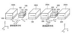
ここで、磁気抵抗素子の感度((dR/R)/2Hs)は、第1の線形応答磁性体160F等の構成によって調整することができる。図13(a)及び(b)には、2つの磁気抵抗素子について異なる磁場感度を得るために、第1の線形応答磁性体160F及び第2の磁性体260Fの構成に差を設けた例を示す。尚、図13(a)及び(b)では、2つの磁気抵抗素子について例にとっているが、3つ以上の磁気抵抗素子としてもよい。  Here, the sensitivity ((dR / R) / 2Hs) of the magnetoresistive element can be adjusted by the configuration of the first linear responsemagnetic body 160F and the like. FIGS. 13A and 13B show an example in which a difference is provided in the configuration of the first linear responsemagnetic body 160F and the secondmagnetic body 260F in order to obtain different magnetic field sensitivities for the two magnetoresistive elements. Show. In FIGS. 13A and 13B, two magnetoresistive elements are taken as an example, but three or more magnetoresistive elements may be used.

図13(a)に示すとおり、磁気抵抗素子と第1及び第2の線形応答磁性体160F,260Fとの間の距離を変えることで、磁界を変えることが可能である。図13(a)に示す第1の磁気抵抗素子100と第1の線形応答磁性体160Fの間の距離Lは、第2の磁気抵抗素子200と第2の線形応答磁性体260Fの間の距離Lよりも大きく設定されている。この場合、第1又は第2の線形応答磁性体160F,260Fから距離が大きいほど、第1又は第2の磁気抵抗素子100,200に加わる磁界は小さくなる。従って、第1の磁気抵抗素子100の飽和磁場Hsは小さくなり、第1の磁気抵抗素子100の磁場感度((dR/R)/2Hs)は、第2の磁気抵抗素子200と比較して高く設定される。As shown in FIG. 13A, the magnetic field can be changed by changing the distance between the magnetoresistive element and the first and second linear responsemagnetic bodies 160F and 260F. Figure 13 the distanceL 1 between thefirst magnetoresistance element 100 first linear response magnetic 160F shown in (a), the second magnetoresistive element 200 between the second linear response magnetic 260F It is set larger than the distance L2. In this case, the greater the distance from the first or second linear responsemagnetic body 160F, 260F, the smaller the magnetic field applied to the first or secondmagnetoresistive element 100, 200. Therefore, the saturation magnetic field Hs of the firstmagnetoresistive element 100 is reduced, and the magnetic field sensitivity ((dR / R) / 2Hs) of the firstmagnetoresistive element 100 is higher than that of thesecond magnetoresistive element 200. Is set.

図13(b)に示すとおり、第1及び第2の線形応答磁性体160F,260Fの膜厚を変えることで、磁界を変えることが可能である。図13(b)に示す第1の線形応答磁性体160Fの膜厚tは、第2の線形応答磁性体260Fの膜厚tよりも小さく設定されている。この場合、第1又は第2の線形応答磁性体160F,260Fの膜厚が厚いほど、第1又は第2の線形応答磁性体160F,260Fの磁気体積が大きくなる。従って、第1の磁気抵抗素子100の飽和磁場Hsは小さくなり、第1の磁気抵抗素子100の磁場感度((dR/R)/2Hs)は、第2の磁気抵抗素子200と比較して高く設定される。As shown in FIG. 13B, the magnetic field can be changed by changing the film thickness of the first and second linear responsemagnetic bodies 160F and 260F. The film thickness t1 of thefirst linear responsemagnetic body 160F shown in FIG. 13B is set smaller than the film thickness t2 of thesecond linear responsemagnetic body 260F. In this case, the larger the film thickness of the first or second linear responsemagnetic body 160F, 260F, the larger the magnetic volume of the first or second linear responsemagnetic body 160F, 260F. Therefore, the saturation magnetic field Hs of the firstmagnetoresistive element 100 is reduced, and the magnetic field sensitivity ((dR / R) / 2Hs) of the firstmagnetoresistive element 100 is higher than that of thesecond magnetoresistive element 200. Is set.

図13(b)では、第1及び第2の線形応答磁性体160F,260Fの膜厚を変えることで磁気体積を変えた場合について説明したが、第1及び第2の線形応答磁性体160F,260Fに用いられる磁性材料の種類を変えることでも磁気体積を変えることができる。例えば、第1の線形応答磁性体160Fと第2の線形応答磁性体260Fのそれぞれに飽和磁化の異なる磁性材料を用いることで、磁気体積を変え、第1および第2の磁気抵抗素子100,200の磁場感度((dR/R)/2Hs)を変えることも出来る。  In FIG. 13B, the case where the magnetic volume is changed by changing the film thickness of the first and second linear responsemagnetic bodies 160F, 260F has been described. However, the first and second linear responsemagnetic bodies 160F, The magnetic volume can also be changed by changing the type of magnetic material used for 260F. For example, by using magnetic materials having different saturation magnetizations for the first linear responsemagnetic body 160F and the second linear responsemagnetic body 260F, the magnetic volume is changed, and the first and secondmagnetoresistive elements 100, 200 are changed. The magnetic field sensitivity ((dR / R) / 2Hs) can be changed.

また、前述したように第1及び第2の線形応答磁性体160F,260Fの面積を変えることで、磁界を変えることが可能である。第1及び第2の線形応答磁性体160F,260Fを第1及び第2の磁気抵抗素子100,200に対して積層方向に配置する場合、第1及び第2の線形応答磁性体160F,260Fの端部と第1及び第2の磁気抵抗素子100,200の端部の距離が離れるほど、第1及び第2の磁気抵抗素子100,200に加わる磁界は小さくなり、第1及び第2の磁気抵抗素子100,200の磁場感度((dR/R)/2Hs)は高くなる。  Further, as described above, the magnetic field can be changed by changing the areas of the first and second linear responsemagnetic bodies 160F and 260F. When the first and second linear responsemagnetic bodies 160F and 260F are arranged in the stacking direction with respect to the first and secondmagnetoresistive elements 100 and 200, the first and second linear responsemagnetic bodies 160F and 260F The greater the distance between the end and the end of the first and secondmagnetoresistive elements 100, 200, the smaller the magnetic field applied to the first and secondmagnetoresistive elements 100, 200, and the first and second magnetic resistance elements. The magnetic field sensitivity ((dR / R) / 2Hs) of theresistance elements 100 and 200 is increased.

また、図9(a)〜(c)の、平面方向から第1の線形応答磁性体160を隣接させた場合と同じように、積層方向に配置した第1の線形応答磁性体160においても形状を変えた1つの第1の線形応答磁性体160で複数の磁気抵抗素子の感度を調整してもよい。  9A to 9C, the first linear responsemagnetic body 160 arranged in the stacking direction is shaped similarly to the case where the first linear responsemagnetic body 160 is adjacent from the planar direction. The sensitivity of a plurality of magnetoresistive elements may be adjusted by one first linear responsemagnetic body 160 with different values.

[1−8.インスタック型の線形応答磁性体]
次に、線形応答磁性体を磁気抵抗素子に包含する場合の磁気抵抗素子と線形応答磁性体との関係について説明する。以下の説明においては、第1の磁気抵抗素子100と第1の線形応答磁性体160を例として説明するが第2の磁気抵抗素子200や第2の線形応答磁性体260等も同様に構成することが可能である。
[1-8. In-stack linear response magnet]
Next, the relationship between the magnetoresistive element and the linear response magnetic body when the linear response magnetic body is included in the magnetoresistive element will be described. In the following description, the firstmagnetoresistive element 100 and the first linear responsemagnetic body 160 will be described as an example. However, thesecond magnetoresistive element 200, the second linear response magnetic body 260, and the like are configured similarly. It is possible.

図14には、本実施の形態に係る第1の磁気抵抗素子100と第1の線形応答磁性体160Gの模式図を示す。第1の線形応答磁性体160Gは、第1の線形応答磁性体160の一態様である。  In FIG. 14, the schematic diagram of the1st magnetoresistive element 100 and the 1st linear responsemagnetic body 160G which concern on this Embodiment is shown. The first linear responsemagnetic body 160G is an embodiment of the first linear responsemagnetic body 160.

図14に示す態様においては、第1の磁気抵抗素子100が第1の線形応答磁性体160Gを包含している。第1の線形応答磁性体160Gは、積層構造からなるインスタックバイアス層として構成される。従って、第1の線形応答磁性体160Gは、内部に含まれるバイアス磁性層の磁化と磁化自由層の間の交換結合磁界により、第1の磁気抵抗素子100の磁場感度を調整することができる。例えば、第1の磁性層160Gの磁化方向を被測定電流から生ずる誘導磁界と略垂直に設定することで、上述した第1の線形応答磁性体160Aを用いた場合と同様の効果を得ることが可能である。  In the embodiment shown in FIG. 14, the firstmagnetoresistive element 100 includes a first linear responsemagnetic body 160G. The first linear responsemagnetic body 160G is configured as an in-stack bias layer having a laminated structure. Therefore, the first linear responsemagnetic body 160G can adjust the magnetic field sensitivity of the firstmagnetoresistive element 100 by the exchange coupling magnetic field between the magnetization of the bias magnetic layer and the magnetization free layer included therein. For example, by setting the magnetization direction of the firstmagnetic layer 160G to be substantially perpendicular to the induced magnetic field generated from the current to be measured, the same effect as that obtained when the first linear responsemagnetic body 160A described above is used can be obtained. Is possible.

図14に表した態様において、第1の線形応答磁性体160Gは、分離層162と、第1バイアス磁性層163と、バイアス磁気結合層164と、第2バイアス磁性層165と、バイアスピニング層166とを含む。  In the embodiment shown in FIG. 14, the first linear responsemagnetic body 160G includes theseparation layer 162, the first biasmagnetic layer 163, the biasmagnetic coupling layer 164, the second biasmagnetic layer 165, and thebias pinning layer 166. Including.

第1バイアス磁性層163および第2バイアス磁性層165は、例えば、磁性材料によって形成される。第2バイアス磁性層165の磁化は、バイアスピニング層166によって一方向に固定される。第1バイアス磁性層163の磁化は、バイアス磁気結合層164を介して隣り合う第2バイアス磁性層165の磁化とは反対に設定される。一方向に磁化が固定された第1バイアス磁性層163は、交換結合などの磁気的結合によって、第1磁性層101にバイアスを加える。このような、バイアス磁性層とバイアスピニング層の積層構造からなる線形応答磁性体160Gを用いた場合、被測定電流として瞬間的に大電流が流れ、大きい誘導磁界が第1の線形応答磁性体160Gに加わった場合においても、第1の線形応答磁性体160Gの磁化の向きを容易に保持することが出来る。  The first biasmagnetic layer 163 and the second biasmagnetic layer 165 are made of, for example, a magnetic material. The magnetization of the second biasmagnetic layer 165 is fixed in one direction by thebias pinning layer 166. The magnetization of the first biasmagnetic layer 163 is set to be opposite to the magnetization of the second biasmagnetic layer 165 adjacent via the biasmagnetic coupling layer 164. The first biasmagnetic layer 163 whose magnetization is fixed in one direction applies a bias to the firstmagnetic layer 101 by magnetic coupling such as exchange coupling. When such a linear responsemagnetic body 160G having a laminated structure of a bias magnetic layer and a bias pinning layer is used, a large current instantaneously flows as a current to be measured, and a large induced magnetic field is generated by the first linear responsemagnetic body 160G. Even in the case of being added to, the magnetization direction of the first linear responsemagnetic body 160G can be easily maintained.

分離層162は、例えば、非磁性材料などから形成され、第1バイアス磁性層163と第1磁性層101とを物理的に分離することで、第1バイアス磁性層163と第1磁性層101との間の磁気的結合の強度を調整する。なお、第1バイアス磁性層163の材料によっては、分離層162は必ずしも設けられなくともよい。図14のように、複数のオフセット磁性層の磁化を反平行(180°)とすることで、バイアス磁性層から外部への漏洩磁界を抑え、磁化自由層への交換結合によるバイアス印加以外の磁気的干渉を抑えることができる。  Theseparation layer 162 is made of, for example, a nonmagnetic material or the like, and physically separates the first biasmagnetic layer 163 and the firstmagnetic layer 101, so that the first biasmagnetic layer 163 and the firstmagnetic layer 101 are separated from each other. Adjust the strength of magnetic coupling between. Note that theseparation layer 162 is not necessarily provided depending on the material of the first biasmagnetic layer 163. As shown in FIG. 14, by making the magnetizations of the plurality of offset magnetic layers antiparallel (180 °), the leakage magnetic field from the bias magnetic layer to the outside is suppressed, and magnetism other than bias application by exchange coupling to the magnetization free layer is performed. Interference can be suppressed.

第1の線形応答磁性体160Gは、図14で示すように、第1バイアス磁性層163/バイアス磁気結合層164/第2バイアス磁性層165を含んでいるが、分離層162とバイアスピニング層166の間に単層の第1バイアス磁性層163のみを設けることによって構成してもよい。また、第1バイアス磁性層/第1磁気結合層/第2バイアス磁性層/第2磁気結合層/第3バイアス磁性層のように、オフセット磁性層の層数を3層以上としてもよい。  As shown in FIG. 14, the first linear responsemagnetic body 160G includes a first biasmagnetic layer 163 / biasmagnetic coupling layer 164 / second biasmagnetic layer 165, but includes aseparation layer 162 and abias pinning layer 166. Alternatively, a single-layer first biasmagnetic layer 163 may be provided therebetween. The number of offset magnetic layers may be three or more, such as first bias magnetic layer / first magnetic coupling layer / second bias magnetic layer / second magnetic coupling layer / third bias magnetic layer.

分離層162には、例えば、5nmのCuが用いられる。第1バイアス磁性層163には、例えば、3nmのFe50Co50が用いられる。バイアス磁気結合層164には、例えば、0.9nmのRuが用いられる。第2バイアス磁性層165には、例えば、3nmのFe50Co50が用いられる。バイアスピニング層166には、例えば、7nmのIrMnが用いられる。For theseparation layer 162, for example, 5 nm of Cu is used. For the first biasmagnetic layer 163, for example, 3 nm of Fe50 Co50 is used. For the biasmagnetic coupling layer 164, for example, Ru of 0.9 nm is used. For the second biasmagnetic layer 165, for example, Fe50 Co50 of 3 nm is used. For thebias pinning layer 166, for example, 7 nm IrMn is used.

第1バイアス磁性層163および第2バイアス磁性層165には、例えば、Co、Fe及びNiよりなる群から選択された少なくともいずれかを用いることができる。第1バイアス磁性層163として、Co、Fe及びNiよりなる群から選択された少なくとも1つの材料を含む合金を用いてもよい。例えば、第1バイアス磁性層163には、CoFe100−x合金(xは0at.%以上100at.%以下)、NiFe100−x合金(xは0at.%以上100at.%以下)、または、これらに非磁性元素を添加した材料が用いられる。第1バイアス磁性層163として、(CoFe100−x100−y合金(xは0at.%以上100at.%以下、yは0at.%以上30at.%以下)が用いられてもよい。For the first biasmagnetic layer 163 and the second biasmagnetic layer 165, for example, at least one selected from the group consisting of Co, Fe, and Ni can be used. As the first biasmagnetic layer 163, an alloy containing at least one material selected from the group consisting of Co, Fe, and Ni may be used. For example, the first biasmagnetic layer 163 includes a Cox Fe100-x alloy (x is 0 at.% Or more and 100 at.% Or less), a Nix Fe100-x alloy (x is 0 at.% Or more and 100 at.% Or less). Or the material which added the nonmagnetic element to these is used. As the first bias magnetic layer163, (Co x Fe 100- x) 100-y B y alloys (x is 0 atomic.% Or more 100 atomic.% Or less, y is 0 atomic.% Or more 30 at.% Or less) even if used Good.

分離層162には、例えば、非磁性材料が用いられる。分離層43は、例えば、Cu、Ru、Rh、Ir、V、Cr、Nb、Mo、Ta、W、Rr、Au、Ag、Pt、Pd、Ti、Zr、Hf、及び、Hfの群から選択された少なくとも一つの元素を含む層を用いることができる。  For example, a nonmagnetic material is used for theseparation layer 162. The separation layer 43 is, for example, selected from the group of Cu, Ru, Rh, Ir, V, Cr, Nb, Mo, Ta, W, Rr, Au, Ag, Pt, Pd, Ti, Zr, Hf, and Hf A layer containing at least one element formed can be used.

バイアスピニング層166は、バイアスピニング層に接して形成される第2バイアス磁性層165に、一方向異方性(Unidirectional Anisotropy)を付与して第1オフセット磁性層163の磁化を固定する。バイアスピニング層166には、例えば、反強磁性層が用いられる。バイアスピニング層166には、例えば、Ir−Mn、Pt−Mn、Pd−Pt−Mn、Ru−Mn、Rh−Mn、Ru−Rh−Mn、Fe−Mn、Ni−Mn、Cr−Mn−PtおよびNi−Oよりなる群から選択された少なくともいずれかが用いられる。Ir−Mn、Pt−Mn、Pd−Pt−Mn、Ru−Mn、Rh−Mn、Ru−Rh−Mn、Fe−Mn、Ni−Mn、Cr−Mn−PtおよびNi−Oにさらに添加元素を加えた合金を用いても良い。十分な強さの一方向異方性を付与するために、バイアスピニング層166の厚さは適切に設定される。  Thebias pinning layer 166 imparts unidirectional anisotropy to the second biasmagnetic layer 165 formed in contact with the bias pinning layer to fix the magnetization of the first offsetmagnetic layer 163. For thebias pinning layer 166, for example, an antiferromagnetic layer is used. Thebias pinning layer 166 includes, for example, Ir—Mn, Pt—Mn, Pd—Pt—Mn, Ru—Mn, Rh—Mn, Ru—Rh—Mn, Fe—Mn, Ni—Mn, and Cr—Mn—Pt. And at least one selected from the group consisting of Ni-O is used. Ir—Mn, Pt—Mn, Pd—Pt—Mn, Ru—Mn, Rh—Mn, Ru—Rh—Mn, Fe—Mn, Ni—Mn, Cr—Mn—Pt and Ni—O further added elements An added alloy may be used. In order to impart sufficient strength of unidirectional anisotropy, the thickness of thebias pinning layer 166 is appropriately set.

バイアスピニング層166としてPtMnまたはPdPtMnが用いられる場合には、バイアスピニング層の厚さは、8nm以上20nm以下が好ましい。バイアスピニング層166の厚さは、10nm以上15nm以下がより好ましい。バイアスピニング層166としてIrMnが用いられる場合には、バイアスピニング層166としてPtMnが用いられる場合よりも薄いバイアスピニング層166で、一方向異方性を第1バイアス磁性層163に付与することができる。この場合には、バイアスピニング層166の厚さは、4nm以上18nm以下が好ましい。バイアスピニング層166の厚さは、5nm以上15nm以下がより好ましい。  When PtMn or PdPtMn is used as thebias pinning layer 166, the thickness of the bias pinning layer is preferably 8 nm or more and 20 nm or less. The thickness of thebias pinning layer 166 is more preferably 10 nm or more and 15 nm or less. When IrMn is used as thebias pinning layer 166, unidirectional anisotropy can be imparted to the first biasmagnetic layer 163 with a thinnerbias pinning layer 166 than when PtMn is used as thebias pinning layer 166. . In this case, the thickness of thebias pinning layer 166 is preferably 4 nm or more and 18 nm or less. The thickness of thebias pinning layer 166 is more preferably 5 nm or more and 15 nm or less.

バイアスピニング層166として、ハード磁性層(硬質強磁性材料)が用いられてもよい。例えば、Co−Pt、Fe−Pt、Co−Pd、Fe−Pdなどの磁気異方性および保磁力が比較的高いハード磁性材料(硬質強磁性材料)が用いられる。また、Co−Pt、Fe−Pt、Co−Pd、Fe−Pdにさらに添加元素を加えた合金を用いても良い。ハード磁性層として、例えば、CoPt(Coの比率は、50at.%以上85at.%以下)、(CoPt100−x100−yCr(xは50at.%以上85at.%以下、yは0at.%以上40at.%以下)、または、FePt(Ptの比率は40at.%以上60%at.以下)などが用いられてもよい。As thebias pinning layer 166, a hard magnetic layer (hard ferromagnetic material) may be used. For example, a hard magnetic material (hard ferromagnetic material) having a relatively high magnetic anisotropy and coercive force such as Co—Pt, Fe—Pt, Co—Pd, and Fe—Pd is used. Alternatively, an alloy obtained by further adding an additive element to Co—Pt, Fe—Pt, Co—Pd, or Fe—Pd may be used. As a hard magnetic layer, for example, CoPt (ratio of Co is, 50at.% Or more 85 at.% Orless), (Co x Pt 100- x) is100-y Cr y (x 50at .% Or more 85 at.% Or less, y May be 0 at.% Or more and 40 at.% Or less), or FePt (the ratio of Pt is 40 at.% Or more and 60% at. Or less).

バイアス磁気結合層165は、第1バイアス磁性層163と第2バイアス磁性層165との間に反強磁性結合を生じさせる。バイアス磁気結合層165は、シンセティックピン構造を形成する。第1磁気結合層として、例えば、Ruが用いられる。第1磁気結合層の厚さは、0.8nm以上1nm以下であることが好ましい。第1バイアス磁性層163と第2バイアス磁性層165との間に十分な反強磁性結合を生じさせる材料であれば、バイアス磁気結合層165としてRu以外の材料を用いてもよい。バイアス磁気結合層164の厚さは、RKKY(Ruderman-Kittel-Kasuya-Yosida)結合のセカンドピーク(2ndピーク)に対応する0.8nm以上1nm以下の厚さに設定することができる。さらに、バイアス磁気結合層164の厚さは、RKKY結合のファーストピーク(1stピーク)に対応する0.3nm以上0.6nm以下の厚さに設定してもよい。第1磁気結合層として、例えば、0.9nmの厚さのRuが用いられる。これにより、高信頼性の結合がより安定して得られる。  The biasmagnetic coupling layer 165 generates antiferromagnetic coupling between the first biasmagnetic layer 163 and the second biasmagnetic layer 165. The biasmagnetic coupling layer 165 forms a synthetic pin structure. For example, Ru is used as the first magnetic coupling layer. The thickness of the first magnetic coupling layer is preferably 0.8 nm or more and 1 nm or less. Any material other than Ru may be used for the biasmagnetic coupling layer 165 as long as the material generates sufficient antiferromagnetic coupling between the first biasmagnetic layer 163 and the second biasmagnetic layer 165. The thickness of the biasmagnetic coupling layer 164 can be set to a thickness of 0.8 nm or more and 1 nm or less corresponding to a second peak (2nd peak) of RKKY (Ruderman-Kittel-Kasuya-Yosida) coupling. Furthermore, the thickness of the biasmagnetic coupling layer 164 may be set to a thickness of 0.3 nm to 0.6 nm corresponding to the first peak (1st peak) of the RKKY coupling. As the first magnetic coupling layer, for example, Ru having a thickness of 0.9 nm is used. Thereby, highly reliable coupling can be obtained more stably.

第1バイアス磁性層163の厚さは、例えば、1.5nm以上5nm以下が好ましい。第2バイアス磁性層165の厚さは、例えば、1.5nm以上5nm以下が好ましい。これにより、例えば、バイアスピニング層166による一方向異方性磁界の強度をより強くすることができる。第1バイアス磁性層163の磁気膜厚(飽和磁化Bsと厚さtとの積(Bs・t))は、第2バイアス磁性層165の磁気膜厚と実質的に等しいことが好ましい。  The thickness of the first biasmagnetic layer 163 is preferably, for example, not less than 1.5 nm and not more than 5 nm. The thickness of the second biasmagnetic layer 165 is preferably, for example, not less than 1.5 nm and not more than 5 nm. Thereby, for example, the strength of the unidirectional anisotropic magnetic field by thebias pinning layer 166 can be further increased. The magnetic film thickness (product of saturation magnetization Bs and thickness t (Bs · t)) of the first biasmagnetic layer 163 is preferably substantially equal to the magnetic film thickness of the second biasmagnetic layer 165.

第1の線形応答磁性体160Gから第1磁性層101に加わるバイアス磁界の方向は、第2磁性層102の磁化方向に対して、任意の方向とすることが可能である。  The direction of the bias magnetic field applied to the firstmagnetic layer 101 from the first linear responsemagnetic body 160 </ b> G can be any direction with respect to the magnetization direction of the secondmagnetic layer 102.

図14(b)は、第1の線形応答磁性体160Gにおける磁化方向の設定方法を説明するための模式図である。例えば、第2磁性層102の磁化方向に対して、第1の線形応答磁性体160Gから第1磁性層101に加わるバイアス磁界の方向を90°(若しくは270℃)に設定することも可能である。このようなバイアス磁界の方向の設定は、2段階の磁界中アニール、並びに、ピニング層105に用いられる材料構成及びバイアスピニング層166に用いられる材料構成の選択によって可能となる。  FIG. 14B is a schematic diagram for explaining a method of setting the magnetization direction in the first linear responsemagnetic body 160G. For example, the direction of the bias magnetic field applied to the firstmagnetic layer 101 from the first linear responsemagnetic body 160G can be set to 90 ° (or 270 ° C.) with respect to the magnetization direction of the secondmagnetic layer 102. . Such setting of the direction of the bias magnetic field can be performed by two-stage annealing in the magnetic field and selection of the material configuration used for the pinninglayer 105 and the material configuration used for thebias pinning layer 166.

ピニング層105またはバイアスピニング層166に用いられる反強磁性材料については、その組成によって磁化固着が生ずる温度が異なる。例えば、PtMnなど規則合金系の材料については、IrMnなどの不規則でも磁化固着を生ずる材料にくらべて、磁化固着が行われる温度が高い。例えば、ピニング層105にPtMnを用い、バイアスピニング層166にIrMnを用いることが可能である。  With respect to the antiferromagnetic material used for the pinninglayer 105 or thebias pinning layer 166, the temperature at which magnetization fixation occurs differs depending on the composition. For example, an ordered alloy-based material such as PtMn has a higher temperature at which magnetization fixation is performed compared to a material that causes magnetization fixation even with irregularities such as IrMn. For example, PtMn can be used for the pinninglayer 105 and IrMn can be used for thebias pinning layer 166.

次に、図14(b)に示すような2段階の磁界中熱処理を行う。例えば、図14(b)の(1)に表すように、図14(b)の右方向に磁場を印加しつつ320℃において10時間アニールを行う。これにより、ピニング層105に接した第2磁化固定層106の磁化方向は、右向きに固着される。また、バイアスピニング層166に接した第2バイアス磁性層165の磁化方向は、いったん右向きに固着される。  Next, a two-stage heat treatment in a magnetic field as shown in FIG. For example, as shown in (1) of FIG. 14B, annealing is performed at 320 ° C. for 10 hours while applying a magnetic field in the right direction of FIG. 14B. Thereby, the magnetization direction of the second magnetization fixedlayer 106 in contact with the pinninglayer 105 is fixed to the right. The magnetization direction of the second biasmagnetic layer 165 in contact with thebias pinning layer 166 is once fixed to the right.

次に、例えば、図13(b)の(2)に表すように、図15(b)の左方向に磁場を印加しつつ260℃において1時間アニールを行う。これにより、ピニング層105に接した第2磁化固定層106の磁化方向は右向きのまま変化せず、バイアスピニング層166に接した第2バイアス磁性層165の磁化方向は、左向きに固着される。この磁化の向きは、図13(b)の右図に示すように、室温においても保持される。  Next, for example, as shown in (2) of FIG. 13B, annealing is performed at 260 ° C. for 1 hour while applying a magnetic field in the left direction of FIG. 15B. As a result, the magnetization direction of the second magnetization fixedlayer 106 in contact with the pinninglayer 105 remains rightward, and the magnetization direction of the second biasmagnetic layer 165 in contact with thebias pinning layer 166 is fixed to the left. This magnetization direction is maintained even at room temperature, as shown in the right figure of FIG.

このように、磁界中アニールの方法、並びに、ピニング層105の材料構成及びバイアスピニング層166の材料構成の選択によって、第1の磁性層101及び第2の磁性層102へのバイアス磁界の方向を任意に設定することが可能である。そのほか、ピニング層105とバイアスピニング層166の磁化固着の温度差は、それぞれの材料の選定のみでなく、それぞれの層の膜厚で設定することも可能である。例えば、ピニング層105にIrMn7nmを用い、バイアスピニング層166にIrMn5nmを用いた場合においても、図14(b)に示した磁界中2段階アニールを行うことで、図14(a)に示したような磁化方向のアライメントを行うことが可能である。  As described above, the direction of the bias magnetic field to the firstmagnetic layer 101 and the secondmagnetic layer 102 is determined by the method of annealing in a magnetic field and the selection of the material configuration of the pinninglayer 105 and the material configuration of thebias pinning layer 166. It is possible to set arbitrarily. In addition, the temperature difference in magnetization fixation between the pinninglayer 105 and thebias pinning layer 166 can be set not only by selection of each material but also by the film thickness of each layer. For example, even when IrMn 7 nm is used for the pinninglayer 105 andIrMn 5 nm is used for thebias pinning layer 166, the two-step annealing in the magnetic field shown in FIG. 14B is performed, as shown in FIG. It is possible to perform alignment in a proper magnetization direction.

ここで、磁気抵抗素子の磁場感度((dR/R)/2Hs)は、インスタックバイアス層の構成によって調整することができる。例えば、第1の磁気抵抗素子100及び第1の線形応答磁性体160Gを図14に示すように構成し、更に第2の磁気抵抗素子200及び第2の線形応答磁性体260をこれらと同様に構成する。但し、第2の線形応答磁性体260においては、第1の磁気抵抗素子160Gと比較して分離層162を厚くする。これによって、第1の磁気抵抗素子100のほうが、バイアス磁界が相対的に弱まる。そのほか、第1バイアス磁性層163と第2バイアス磁性層165の厚みを2つの磁気抵抗素子で差をつけることによってもバイアス磁界を変えることが可能である。この場合、第1バイアス磁性層163と第2バイアス磁性層165の厚みを厚くしたほうが、第1磁性層101に加わるバイアス磁界が弱まる。従って、飽和磁化Hsは低くなり、感度((dR/R)/2Hs)は高く設定させる。  Here, the magnetic field sensitivity ((dR / R) / 2Hs) of the magnetoresistive element can be adjusted by the configuration of the in-stack bias layer. For example, the firstmagnetoresistive element 100 and the first linear responsemagnetic body 160G are configured as shown in FIG. 14, and thesecond magnetoresistive element 200 and the second linear response magnetic body 260 are configured similarly to these. Configure. However, in the second linear response magnetic body 260, theseparation layer 162 is made thicker than the firstmagnetoresistive element 160G. As a result, the bias magnetic field is relatively weaker in the firstmagnetoresistive element 100. In addition, it is also possible to change the bias magnetic field by differentiating the thicknesses of the first biasmagnetic layer 163 and the second biasmagnetic layer 165 with two magnetoresistive elements. In this case, the bias magnetic field applied to the firstmagnetic layer 101 is weakened as the thickness of the first biasmagnetic layer 163 and the second biasmagnetic layer 165 is increased. Therefore, the saturation magnetization Hs is lowered, and the sensitivity ((dR / R) / 2Hs) is set high.

尚、ここまでの説明では、第1の線形応答磁性体160Gの磁化方向を設定するために2段階の磁界中アニールを行う事について説明した。ここで、このような2段階の磁界中アニールを用いた場合、第1の磁性層101の磁化方向を設定することも可能である。図15は、この為の方法を説明するための模式図である。このような方法によっても、例えば、図3(b)に示すように、磁化自由層の磁化方向を磁化固定層の磁化方向と直交させ、図3(d)に示すように正負の磁界に線形的に感応させることができる。  In the above description, the two-stage annealing in the magnetic field is performed in order to set the magnetization direction of the first linear responsemagnetic body 160G. Here, when such two-step annealing in a magnetic field is used, the magnetization direction of the firstmagnetic layer 101 can also be set. FIG. 15 is a schematic diagram for explaining a method for this purpose. Also by such a method, for example, as shown in FIG. 3B, the magnetization direction of the magnetization free layer is orthogonal to the magnetization direction of the magnetization fixed layer, and linearly changes to a positive and negative magnetic field as shown in FIG. Can be sensitive.

第1磁性層101の磁化方向と第2磁性層102の磁化方向を異なる方向に設定するためには、例えば、図15(b)の左図に示すように、第1の磁界中熱処理を行う。第1の磁界中熱処理は、例えば図15(b)の右方向に磁場を印加しつつ320℃において10時間アニールを行うことによって行われる。これにより、ピニング層105に接した第2磁化固定層106の磁化方向は、右向きに固着される。  In order to set the magnetization direction of the firstmagnetic layer 101 and the magnetization direction of the secondmagnetic layer 102 to different directions, for example, as shown in the left diagram of FIG. . The first heat treatment in a magnetic field is performed, for example, by annealing for 10 hours at 320 ° C. while applying a magnetic field in the right direction in FIG. Thereby, the magnetization direction of the second magnetization fixedlayer 106 in contact with the pinninglayer 105 is fixed to the right.

次に、例えば、第2の磁界中熱処理を行う。第2の磁界中熱処理は、例えば図15(b)の中図に示すように、図15(b)の上方向に磁場を印加しつつアニールを行うことによって行う。この際の温度は、320℃よりも低温であり、且つバイアスピニング層166に用いる反強磁性体の磁化固着温度よりも低温に設定する。これにより、第2磁化固定層106の磁化方向を右向きにしたままで、第1磁性層101の磁化方向を上向きに設定することができる。即ち、第1磁性層101の誘導磁気異方性の方向を上下方向に設定することが出来る。  Next, for example, a second heat treatment in a magnetic field is performed. The second heat treatment in a magnetic field is performed, for example, by annealing while applying a magnetic field upward in FIG. 15B, as shown in the middle diagram of FIG. The temperature at this time is set lower than 320 ° C. and lower than the magnetization fixed temperature of the antiferromagnetic material used for thebias pinning layer 166. As a result, the magnetization direction of the firstmagnetic layer 101 can be set upward while the magnetization direction of the second magnetization fixedlayer 106 remains rightward. That is, the direction of the induced magnetic anisotropy of the firstmagnetic layer 101 can be set to the up and down direction.

ここで、磁気抵抗素子の磁場感度((dR/R)/2Hs)は、2段階アニールの第2の磁界中熱処理の温度や時間によって調整することができる。例えば、第1の磁気抵抗素子100と第2の磁気抵抗素子200を作製し、第1の磁気抵抗素子100製造時の第2の磁界中熱処理の時間を第2の磁気抵抗素子200製造時の第2の磁界中熱処理の時間よりも長時間とすることによって、第2の磁気抵抗素子200の第1磁性層の誘導磁気異方性が第1の磁気抵抗素子100のそれよりも高くなるため、Hsが大きくなり、磁場感度((dR/R)/2Hs)は低く設定される。  Here, the magnetic field sensitivity ((dR / R) / 2Hs) of the magnetoresistive element can be adjusted by the temperature and time of the second magnetic field heat treatment in the two-step annealing. For example, the firstmagnetoresistive element 100 and thesecond magnetoresistive element 200 are manufactured, and the time of the second heat treatment in the magnetic field when the firstmagnetoresistive element 100 is manufactured is the same as that when thesecond magnetoresistive element 200 is manufactured. Since the induction magnetic anisotropy of the first magnetic layer of thesecond magnetoresistive element 200 becomes higher than that of the firstmagnetoresistive element 100 by making it longer than the time of the heat treatment in the second magnetic field. , Hs increases, and the magnetic field sensitivity ((dR / R) / 2Hs) is set low.

[1−9.製造方法]
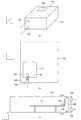
次に、本実施の形態に係る電流センサの製造方法について述べる。図16(a)〜図16(j)は、本実施の形態に係る電流センサの製造方法を例示する工程順模式的斜視図である。
[1-9. Production method]
Next, a method for manufacturing the current sensor according to the present embodiment will be described. FIG. 16A to FIG. 16J are schematic perspective views in order of the processes, illustrating the method for manufacturing the current sensor according to this embodiment.

図16(a)に表したように、基板110上に下部電極E1を形成する。例えば、Ta(5nm)/Cu(200nm)/Ta(35nm)を形成する。この後に、下部電極E1の最表面にCMP処理などの表面平滑化処理を行い、下部電極E1上に形成される構成を平坦にしても良い。  As shown in FIG. 16A, the lower electrode E <b> 1 is formed on thesubstrate 110. For example, Ta (5 nm) / Cu (200 nm) / Ta (35 nm) is formed. Thereafter, a surface smoothing process such as a CMP process may be performed on the outermost surface of the lower electrode E1 to flatten the structure formed on the lower electrode E1.

次に、図16(b)に示すように、下部電極E1の平面形状を加工する。この工程では、レジストをフォトリソグラフィによりパターニングし、その後、図示しないレジストパターンをマスクとして用いて、物理ミリングまたは化学ミリングが実施される。例えば、Arイオンミリングを行う。  Next, as shown in FIG. 16B, the planar shape of the lower electrode E1 is processed. In this step, the resist is patterned by photolithography, and then physical milling or chemical milling is performed using a resist pattern (not shown) as a mask. For example, Ar ion milling is performed.

次に、図16(c)に示すように、下部電極E1の周辺に絶縁層111の埋め込み成膜を行う。この工程では、例えば、リフトオフ工程が行われる。例えば、図16(b)のフォトリソグラフィで形成したレジストパターンは残したままで、全面に絶縁層111を成膜し、その後レジストパターンを除去する。絶縁層111として、例えば、SiO、AlO、SiN及びAlNなどを用いることができる。Next, as shown in FIG. 16C, an insulatingfilm 111 is embedded around the lower electrode E1. In this process, for example, a lift-off process is performed. For example, the insulatinglayer 111 is formed on the entire surface while leaving the resist pattern formed by photolithography in FIG. 16B, and then the resist pattern is removed. For example, SiOx , AlOx , SiNx, and AlNx can be used as the insulatinglayer 111.

次に、下部電極E1上に磁気抵抗素子の電極間の構成を成膜する。例えば、下地層104として、Ta(3nm)/Ru(2nm)を形成する。その上にピニング層105として、IrMn(7nm)を形成する。その上に第2磁性膜102として、Co75Fe25(2.5nm)/Ru(0.9nm)/Co40Fe4020(3nm)を形成する。その上に中間層103として、MgO(2nm)を形成する。その上に第1磁性膜101として、Co40Fe4020(2nm)/Ta(0.4nm)/Ni80Fe20(6nm)を形成する。その上にキャップ層108として、Cu(1nm)/Ta(2nm)/Ru(5nm)を形成する。Next, a structure between the electrodes of the magnetoresistive element is formed on the lower electrode E1. For example, Ta (3 nm) / Ru (2 nm) is formed as thebase layer 104. On top of that, IrMn (7 nm) is formed as a pinninglayer 105. On top of this, Co75 Fe25 (2.5 nm) / Ru (0.9 nm) / Co40 Fe40 B20 (3 nm) is formed as the secondmagnetic film 102. On top of that, MgO (2 nm) is formed as anintermediate layer 103. On top of that, Co40 Fe40 B20 (2 nm) / Ta (0.4 nm) / Ni80 Fe20 (6 nm) is formed as the firstmagnetic film 101. On top of that, Cu (1 nm) / Ta (2 nm) / Ru (5 nm) is formed as acap layer 108.

次に、第2磁性膜102の磁化方向を固着する磁界中アニールを行う。例えば、7kOeの磁場を印加しつつで300℃で一時間のアニールを行う。このアニールは、例えば、誘導磁界印加方向(X方向)に対して、略平行に外部磁界を加えて行う。ここで、例えば、前述したインスタックバイアス層を設けた線形応答磁性体(160G,図14(a))を用いる場合などには、2段階のアニールを行っても良い。  Next, annealing in a magnetic field that fixes the magnetization direction of the secondmagnetic film 102 is performed. For example, annealing is performed for one hour at 300 ° C. while applying a magnetic field of 7 kOe. This annealing is performed, for example, by applying an external magnetic field substantially parallel to the induction magnetic field application direction (X direction). Here, for example, when the linear response magnetic body (160G, FIG. 14A) provided with the in-stack bias layer described above is used, two-stage annealing may be performed.

次に、図16(e)に示すように、磁気抵抗素子の電極間の構成の平面形状を加工する。この工程では、レジストをフォトリソグラフィによりパターニングし、その後、図示しないレジストパターンをマスクとして用いて、物理ミリングまたは化学ミリングが実施される。この工程によって、図16(e)に示すように、複数の構成を一括して加工することができる。  Next, as shown in FIG. 16E, the planar shape of the configuration between the electrodes of the magnetoresistive element is processed. In this step, the resist is patterned by photolithography, and then physical milling or chemical milling is performed using a resist pattern (not shown) as a mask. By this step, as shown in FIG. 16E, a plurality of components can be processed at once.

次に、図16(f)に示すように、磁気抵抗素子の電極間の構成の周辺に絶縁層109の埋め込み成膜を行う。この工程では、例えば、リフトオフ工程が行われる。例えば、図16(e)のフォトリソグラフィで形成したレジストパターンは残したままで、全面に絶縁層109を成膜し、その後レジストパターンを除去する。絶縁層109として、例えば、SiO、AlO、SiN及びAlNなどを用いることができる。Next, as shown in FIG. 16F, an insulatinglayer 109 is embedded in the periphery of the configuration between the electrodes of the magnetoresistive element. In this process, for example, a lift-off process is performed. For example, the insulatinglayer 109 is formed on the entire surface while leaving the resist pattern formed by photolithography in FIG. 16E, and then the resist pattern is removed. As the insulatinglayer 109, for example, SiOx , AlOx , SiNx, AlNx, or the like can be used.

次に、図16(g)に示すように、磁気抵抗素子の電極間の構成に隣接して設ける線形応答磁性体160を埋め込むためのホール109aを形成する。この工程では、レジストをフォトリソグラフィによりパターニングし、その後、図示しないレジストパターンをマスクとして用いて、物理ミリングまたは化学ミリングが実施される。図16(g)では、複数の磁気抵抗素子に対して、一対の第1の線形応答磁性体160Eを形成する場合を例にとっているが、複数の磁気抵抗素子に対して、別個にオフセット磁性体を形成する場合でも一括で加工することができる。この工程において、ホール109aは絶縁層109を貫通するところまで行っても良いし、途中で止めても良い。図16(g)では途中で止めた場合を例示している。後述するが、ホール109aを、絶縁層109を貫通するところまでエッチングした場合には、図16(h)に示す第1のオフセット磁性体150の埋め込み工程において、第1の線形応答磁性体160Eの下に図示しない絶縁層を成膜する必要がある。  Next, as shown in FIG. 16G, ahole 109a for embedding the linear responsemagnetic body 160 provided adjacent to the configuration between the electrodes of the magnetoresistive element is formed. In this step, the resist is patterned by photolithography, and then physical milling or chemical milling is performed using a resist pattern (not shown) as a mask. FIG. 16G shows an example in which a pair of first linear responsemagnetic bodies 160E are formed for a plurality of magnetoresistive elements, but an offset magnetic body is separately provided for a plurality of magnetoresistive elements. Even when forming, it can be processed in a lump. In this step, thehole 109a may be formed up to the point where it penetrates the insulatinglayer 109, or may be stopped halfway. FIG. 16 (g) illustrates a case of stopping in the middle. As will be described later, when thehole 109a is etched to the point where it penetrates the insulatinglayer 109, the first offsetmagnetic body 160E is embedded in the first offset magnetic body 150 embedding step shown in FIG. It is necessary to form an insulating layer (not shown) below.

次に、図16(h)に示すように、図16(g)で形成したホール109aに第1の線形応答磁性体160Eを埋め込む。この工程では、例えば、リフトオフ工程が行われる。例えば、図16(h)のフォトリソグラフィで形成したレジストパターンは残したままで、全面に第1の線形応答磁性体160Eを成膜し、その後レジストパターンを除去する。ここでは、例えば、第1の線形応答磁性体160E用下地層として、Cr(5nm)を形成し、その上に第1の線形応答磁性体160Eとして、例えば、Co80Pt20(20nm)を形成する。その上に、さらに図示しないキャップ層を形成しても良い。このキャップ層として、磁気抵抗素子のキャップ層108に使用可能な材料として上述した材料を用いても良いし、SiO、AlO、SiN及びAlNなどの絶縁層を用いても良い。図16(h)にて、第1の線形応答磁性体160Eを埋め込んだ後に、室温で外部磁界を加えて、第1の線形応答磁性体160Eに含まれるハード磁性層(硬質磁性材料)の磁化方向の設定を行う。例えば、誘導磁界の方向に対して、略垂直な方向に外部磁界の印加を行う。この外部磁界による第1の線形応答磁性体160Eの磁化方向の設定は、第1の線形応答磁性体160Eの埋め込み後であれば、レジストパターンの除去前、除去後、及び図16(j)に示す上部電極E2の加工後のいずれのタイミングに行っても良い。Next, as shown in FIG. 16H, the first linear responsemagnetic body 160E is embedded in thehole 109a formed in FIG. In this process, for example, a lift-off process is performed. For example, the first linear responsemagnetic body 160E is formed on the entire surface while leaving the resist pattern formed by photolithography in FIG. 16H, and then the resist pattern is removed. Here, for example, Cr (5 nm) is formed as an underlayer for the first linear responsemagnetic body 160E, and, for example, Co80 Pt20 (20 nm) is formed as the first linear responsemagnetic body 160E thereon. To do. A cap layer (not shown) may be further formed thereon. As the cap layer, the above-described materials that can be used for thecap layer 108 of the magnetoresistive element may be used, or insulating layers such as SiOx , AlOx , SiNx, and AlNx may be used. In FIG. 16H, after embedding the first linear responsemagnetic body 160E, an external magnetic field is applied at room temperature to magnetize the hard magnetic layer (hard magnetic material) included in the first linear responsemagnetic body 160E. Set the direction. For example, the external magnetic field is applied in a direction substantially perpendicular to the direction of the induction magnetic field. The setting of the magnetization direction of the first linear responsemagnetic body 160E by the external magnetic field is after embedding the first linear responsemagnetic body 160E, before and after the removal of the resist pattern, and in FIG. It may be performed at any timing after the processing of the upper electrode E2 shown.

次に、図16(i)に示すように、上部電極E2を成膜する。次に、図16(j)に示すように、上部電極E2の平面形状を加工する。この工程では、レジストをフォトリソグラフィによりパターニングし、その後、図示しないレジストパターンをマスクとして用いて、物理ミリングまたは化学ミリングが行われる。  Next, as shown in FIG. 16I, the upper electrode E2 is formed. Next, as shown in FIG. 16J, the planar shape of the upper electrode E2 is processed. In this step, the resist is patterned by photolithography, and then physical milling or chemical milling is performed using a resist pattern (not shown) as a mask.

このような態様に係る製造方法によれば、工程数の増加を招くことなく本実施の形態に係る電流センサを製造することが可能である。尚、図16(a)〜(j)では図示していないが、下部電極E1へのコンタクトホールの形成を行っても良いし、上部電極E2の加工後に保護膜を形成しても良い。  According to the manufacturing method according to such an aspect, the current sensor according to the present embodiment can be manufactured without increasing the number of steps. Although not shown in FIGS. 16A to 16J, a contact hole may be formed in the lower electrode E1, or a protective film may be formed after processing the upper electrode E2.

次に、本実施の形態に係る電流センサの別の製造方法について述べる。図17(a)〜図17(j)は、本実施の形態に係る電流センサの別の製造方法を例示する工程順模式的斜視図である。尚、図17(a)〜図17(d)に示す工程は、図16(a)〜図16(d)に示した工程と同様であるため、説明を省略する。  Next, another method for manufacturing the current sensor according to the present embodiment will be described. FIG. 17A to FIG. 17J are schematic perspective views in order of the processes, illustrating another method for manufacturing the current sensor according to the present embodiment. In addition, since the process shown to Fig.17 (a)-FIG.17 (d) is the same as the process shown to Fig.16 (a)-FIG.16 (d), description is abbreviate | omitted.

図17(e)に示すように、磁気抵抗素子の電極間の構成の平面形状を加工する。この工程は、図16(e)に示した工程とほぼ同様に行われるが、積層された第1の磁性膜101等のY方向の寸法を最終的な寸法よりも長くしている点において異なる。  As shown in FIG. 17E, the planar shape of the configuration between the electrodes of the magnetoresistive element is processed. This step is performed in substantially the same manner as the step shown in FIG. 16E, but differs in that the dimension in the Y direction of the laminated firstmagnetic film 101 and the like is longer than the final dimension. .

次に、図17(f)に示すように、積層体の周辺に絶縁層の埋め込み成膜を行う。この工程は、図16(f)に示した工程と同様に行われる。  Next, as shown in FIG. 17F, an embedded insulating layer is formed around the stacked body. This step is performed in the same manner as the step shown in FIG.

次に、図17(g)に示すように、磁気抵抗素子の電極間の構成に隣接して設ける第1の線形応答磁性体160Eを埋め込むためのホール109aを形成する。この工程では、レジストをフォトリソグラフィによりパターニングし、その後、図示しないレジストパターンをマスクとして用いて、物理ミリングまたは化学ミリングが実施される。図17(g)では、複数の磁気抵抗素子に対して、一対の第1の線形応答磁性体160Eを形成する場合を例にとっているが、複数の磁気抵抗素子に対して、別個に線形応答磁性体160を形成する場合でも一括で加工することができる。図17(g)には、ホール109aが絶縁層109を貫通するまでエッチングを行った例を示している。図17(g)に示した例では、このエッチングによって、積層された第1の磁性膜101等のY方向の寸法が最終的な寸法になるように加工を行っている。  Next, as shown in FIG. 17G, ahole 109a for embedding the first linear responsemagnetic body 160E provided adjacent to the configuration between the electrodes of the magnetoresistive element is formed. In this step, the resist is patterned by photolithography, and then physical milling or chemical milling is performed using a resist pattern (not shown) as a mask. FIG. 17G illustrates an example in which a pair of first linear responsemagnetic bodies 160E are formed for a plurality of magnetoresistive elements, but linear response magnetism is separately provided for a plurality of magnetoresistive elements. Even when thebody 160 is formed, it can be processed at once. FIG. 17G shows an example in which etching is performed until thehole 109 a penetrates the insulatinglayer 109. In the example shown in FIG. 17G, the etching is performed so that the dimension in the Y direction of the laminated firstmagnetic film 101 and the like becomes the final dimension.

次に、図17(h)に示すように、図17(g)で形成したホール109aに第1の線形応答磁性体160Eを埋め込む。この工程では、例えば、リフトオフ工程が行われる。例えば、図17(h)のフォトリソグラフィで形成したレジストパターンは残したままで、全面に第1の線形応答磁性体160Eを成膜し、その後レジストパターンを除去する。ここでは、ホール109aが絶縁層109を貫通しているため、第1の線形応答磁性体160Eの埋め込み工程の第1層として、絶縁層112の形成を行う。絶縁層112は、例えば、SiOを10nm製膜することによって形成される。ここで、形成された絶縁層112はホール109aの側壁にも堆積する。従って、その側壁に堆積した絶縁層112によって、磁気抵抗素子と第1の線形応答磁性体160Eとを絶縁し、更にこれらの間の距離を好適に調整することができる。その後、例えば、図16(h)に示した工程と同様の工程によって第1の線形応答磁性体160Eを埋め込む。図17(h)にて、第1の線形応答磁性体160Eを埋め込んだ後に、室温で外部磁界を加えて、第1の線形応答磁性体160Eに含まれる硬質磁性材料の磁化方向の設定を行う。例えば、誘導磁界の方向に対して、略垂直な方向に外部磁界の印加を行う。この外部磁界による第1の線形応答磁性体160Eの磁化方向の設定は、第1の線形応答磁性体160Eの埋め込み後であれば、レジストパターンの除去前、除去後、及び図16(j)に示す上部電極E2の加工後のいずれのタイミングに行っても良い。Next, as shown in FIG. 17H, the first linear responsemagnetic body 160E is embedded in thehole 109a formed in FIG. In this process, for example, a lift-off process is performed. For example, the first linear responsemagnetic body 160E is formed on the entire surface while leaving the resist pattern formed by photolithography in FIG. 17H, and then the resist pattern is removed. Here, since thehole 109a penetrates the insulatinglayer 109, the insulatinglayer 112 is formed as the first layer in the step of embedding the first linear responsemagnetic body 160E. The insulatinglayer 112 is formed, for example, by depositing SiOx to a thickness of 10 nm. Here, the formed insulatinglayer 112 is also deposited on the side wall of thehole 109a. Therefore, the magnetoresistive element and the first linear responsemagnetic body 160E can be insulated from each other by the insulatinglayer 112 deposited on the side wall, and the distance between them can be suitably adjusted. Thereafter, for example, the first linear responsemagnetic body 160E is embedded by a process similar to the process shown in FIG. In FIG. 17H, after embedding the first linear responsemagnetic body 160E, an external magnetic field is applied at room temperature to set the magnetization direction of the hard magnetic material included in the first linear responsemagnetic body 160E. . For example, the external magnetic field is applied in a direction substantially perpendicular to the direction of the induction magnetic field. The setting of the magnetization direction of the first linear responsemagnetic body 160E by the external magnetic field is after embedding the first linear responsemagnetic body 160E, before and after the removal of the resist pattern, and in FIG. It may be performed at any timing after the processing of the upper electrode E2 shown.

次に、図17(i)に示すように、上部電極E2を形成する。次に、図17(j)に示すように、上部電極E2の平面形状を加工する。この工程は、図16(j)を用いて説明した工程と同様に行われる。  Next, as shown in FIG. 17I, the upper electrode E2 is formed. Next, as shown in FIG. 17J, the planar shape of the upper electrode E2 is processed. This step is performed in the same manner as the step described with reference to FIG.

このような態様に係る製造方法によっても、工程数の増加を招くことなく本実施の形態に係る電流センサを製造することが可能である。尚、図17(a)〜(j)では図示していないが、下部電極E1へのコンタクトホールの形成を行っても良いし、上部電極E2の加工後に保護膜を形成しても良い。  Also with the manufacturing method according to such an aspect, the current sensor according to the present embodiment can be manufactured without increasing the number of steps. Although not shown in FIGS. 17A to 17J, a contact hole may be formed in the lower electrode E1, or a protective film may be formed after processing the upper electrode E2.

[2.第2の実施の形態]
[2−1.構成]
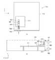
次に、図18及び図19を参照して、第2の実施の形態に係る電流センサについて説明する。図18は、本実施の形態に係る電流センサの一部の概略構成を示す平面図、図19は、同電流センサの構成例を示す概略図である。図19に示す通り、本実施の形態に係る電流センサは、第1の実施の形態に係る電流センサと同様に、配線500の近傍に配置され、この配線500に流れる測定電流からの誘導磁界の印加により抵抗値が変化する第1の磁気抵抗素子100及び第2の磁気抵抗素子200を有する。また、本実施の形態に係る第1の磁気抵抗素子100及び第2の磁気抵抗素子200は、第1の実施の形態と同様に、磁場感度が異なる。しかしながら、本実施の形態に係る磁気抵抗素子は、線形応答磁性体では無く磁束ガイド(例えば図18、図19中の170A)を用いて磁場感度の調整を行っている点において第1の実施の形態と異なる。
[2. Second Embodiment]
[2-1. Constitution]
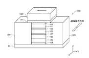
Next, a current sensor according to a second embodiment will be described with reference to FIGS. FIG. 18 is a plan view showing a schematic configuration of a part of the current sensor according to the present embodiment, and FIG. 19 is a schematic diagram showing a configuration example of the current sensor. As shown in FIG. 19, the current sensor according to the present embodiment is arranged in the vicinity of thewiring 500, as in the current sensor according to the first embodiment, and the induced magnetic field from the measurement current flowing through thewiring 500 is It has the1st magnetoresistive element 100 and the 2ndmagnetoresistive element 200 which change resistance value by application. In addition, the firstmagnetoresistive element 100 and thesecond magnetoresistive element 200 according to the present embodiment have different magnetic field sensitivities as in the first embodiment. However, the magnetoresistive element according to the present exemplary embodiment is different from the first exemplary embodiment in that the magnetic field sensitivity is adjusted using a magnetic flux guide (for example, 170A in FIGS. 18 and 19) instead of the linear response magnetic body. Different from form.

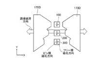
磁束ガイド170は従来のインダクタンス型で用いられている磁性コアと同一の原理で働くものであり、磁気抵抗素子の周辺に配置された高透磁率の磁性体からなる。高誘磁率の磁性体が配置されていた場合、この磁性体を通過する磁束が磁性体の飽和磁束以下である限り、磁束はこの磁性体に引き寄せられる。従って、上記磁束ガイドを使用することにより、磁気抵抗素子に磁束を集中させることが可能である。従って、磁束ガイドの有無、又は構成等の違いにより、磁気抵抗素子に入射する磁束密度(すなわち磁界)に差を設け、磁場感度に差を設けることが可能である。  Themagnetic flux guide 170 works on the same principle as a magnetic core used in a conventional inductance type, and is made of a high-permeability magnetic material disposed around the magnetoresistive element. When a magnetic material with a high magnetic permeability is disposed, the magnetic flux is attracted to the magnetic material as long as the magnetic flux passing through the magnetic material is less than or equal to the saturation magnetic flux of the magnetic material. Therefore, it is possible to concentrate the magnetic flux on the magnetoresistive element by using the magnetic flux guide. Therefore, it is possible to provide a difference in magnetic flux density (that is, a magnetic field) incident on the magnetoresistive element and to provide a difference in magnetic field sensitivity depending on the presence or absence of the magnetic flux guide or the configuration.

図18及び図19に示す通り、本実施の形態に係る電流センサにおいては、第1の磁気抵抗素子100の周辺に、第1の磁束ガイド170Aが配置されている。第1の磁束ガイド170Aは、磁束ガイドの一態様である。また、第2の磁気抵抗素子200の周辺には、磁束ガイドが配置されていない。  As shown in FIGS. 18 and 19, in the current sensor according to the present embodiment, a firstmagnetic flux guide 170 </ b> A is disposed around the firstmagnetoresistive element 100. The firstmagnetic flux guide 170A is an aspect of the magnetic flux guide. Further, no magnetic flux guide is disposed around thesecond magnetoresistive element 200.

磁束ガイド170は、第1の磁気抵抗素子100の、被測定電流からの誘導磁場が印加される方向の側面に配置される。また、磁束ガイド170は台形状に形成されており、第1の磁気抵抗素子100から離れた面170aが、第1の磁気抵抗素子100に対向する面よりも広くなるように形成されている。更に、磁束ガイド170の第1の磁気抵抗素子100に対向する面170bの幅は、第1の磁気抵抗素子100の幅より少し大きい。  Themagnetic flux guide 170 is disposed on the side surface of the firstmagnetoresistive element 100 in the direction in which the induced magnetic field from the current to be measured is applied. Further, themagnetic flux guide 170 is formed in a trapezoidal shape, and thesurface 170 a away from the firstmagnetoresistive element 100 is formed so as to be wider than the surface facing the firstmagnetoresistive element 100. Further, the width of thesurface 170 b of themagnetic flux guide 170 facing the firstmagnetoresistive element 100 is slightly larger than the width of the firstmagnetoresistive element 100.

被測定電流からの誘導磁界は、第1磁性層101の磁化方向に対しては垂直、第2磁性層102の磁化方向に対しては平行に入射する。ここで、磁束ガイド170は高透磁率の磁性体から形成されている為、誘導磁界は磁束ガイド170の面170aに向かって収束し、磁束ガイド170に入射する。また、磁束が出射する面170bの面積は、磁束が入射する面170aの面積と比較して小さい。従って、磁束ガイド170に入射した磁束は更に収束して第1の磁気抵抗素子100に入射する。従って、第1の磁気抵抗素子100に印加される磁界は、磁束ガイド170を設けない場合と比較して大きくなる。  The induced magnetic field from the current to be measured is incident perpendicular to the magnetization direction of the firstmagnetic layer 101 and parallel to the magnetization direction of the secondmagnetic layer 102. Here, since themagnetic flux guide 170 is formed of a magnetic material having a high magnetic permeability, the induced magnetic field converges toward thesurface 170 a of themagnetic flux guide 170 and enters themagnetic flux guide 170. Further, the area of thesurface 170b from which the magnetic flux exits is smaller than the area of thesurface 170a from which the magnetic flux enters. Accordingly, the magnetic flux incident on themagnetic flux guide 170 is further converged and incident on the firstmagnetoresistive element 100. Therefore, the magnetic field applied to the firstmagnetoresistive element 100 is larger than when themagnetic flux guide 170 is not provided.

磁束ガイド170は、種々の高透磁率の軟磁性体(Fe,Co,Niの単体または合金)から形成することが可能であるが、例えばニッケル鉄、コバルトジルコニウムニオブ、鉄アルミニウムシリコン、鉄コバルトニッケルと軟磁性アモルファス合金等の軟磁性材料を適用することが可能である。  Themagnetic flux guide 170 can be formed from various high-permeability soft magnetic materials (single or alloy of Fe, Co, Ni), for example, nickel iron, cobalt zirconium niobium, iron aluminum silicon, iron cobalt nickel. It is possible to apply soft magnetic materials such as soft magnetic amorphous alloys.

ここで、図19においては、磁束ガイド170の有無によって磁場感度((dR/R)/2Hs)に差を設けた例について説明したが、磁気抵抗素子の磁場感度((dR/R)/2Hs)は、磁束ガイド170等の構成によって調整することもできる。図20(a)及び(b)には、第1の磁気抵抗素子100及び第2の磁気抵抗素子200について異なる磁場感度を得るために、第1の磁束ガイド170A及び第2の磁束ガイド270Aの構成に差を設けた例を示す。第2の磁束ガイド270Aは、磁束ガイドの一態様である。尚、図20(a)及び(b)においては、電流センサが2つの磁気抵抗素子を備える例について説明しているが、電流センサは、当然3つ以上の磁気抵抗素子を備えていても良い。また、図20及び図19では、磁気抵抗素子の側方に隣接して第1又は第2の磁束ガイド170A,270Aを設けた場合を例にとり説明しているが、磁気抵抗素子の斜め側方に第1又は第2の磁束ガイド170A,270Aを設けた場合でも、同様に異なる磁場感度を得ることができる。また、図20においては簡略化のために、第1又は第2の磁束ガイド170A,270Aの凸部のみを図示している。  Here, in FIG. 19, the example in which the magnetic field sensitivity ((dR / R) / 2Hs) is different depending on the presence or absence of themagnetic flux guide 170 has been described. However, the magnetic field sensitivity ((dR / R) / 2Hs of the magnetoresistive element is described. ) Can be adjusted by the configuration of themagnetic flux guide 170 or the like. 20A and 20B, in order to obtain different magnetic field sensitivities for the firstmagnetoresistive element 100 and thesecond magnetoresistive element 200, the first magnetic flux guide 170A and the second magnetic flux guide 270A are shown. The example which provided the difference in the structure is shown. The secondmagnetic flux guide 270A is an aspect of the magnetic flux guide. In FIGS. 20A and 20B, an example in which the current sensor includes two magnetoresistive elements is described. However, the current sensor may naturally include three or more magnetoresistive elements. . FIGS. 20 and 19 illustrate the case where the first or second magnetic flux guides 170A and 270A are provided adjacent to the side of the magnetoresistive element, but the oblique side of the magnetoresistive element is illustrated. Even when the first or second magnetic flux guides 170A and 270A are provided, different magnetic field sensitivities can be obtained. In FIG. 20, only the convex portions of the first or second magnetic flux guides 170A and 270A are shown for the sake of simplicity.

図20(a)に示すとおり、磁気抵抗素子と第1及び第2の磁束ガイド170A,270Aとの間の距離を変えることで、磁場感度を変えることが可能である。図20(a)に示す第1の磁気抵抗素子100と一対の磁束ガイド170Aとのそれぞれの間の距離の和L1a+L1bは、第2の磁気抵抗素子200と一対の第2の磁束ガイド270Aのそれぞれの距離の和L2a+L2bよりも大きく設定されている。この場合、第1又は第2の磁束ガイド170A,270Aから距離が大きいほど、第1又は第2の磁気抵抗素子100,200に加わる誘導磁界は小さくなる。第1の磁気抵抗素子100の磁場感度((dR/R)/2Hs)は、第2の磁気抵抗素子200と比較して低く設定される。As shown in FIG. 20A, the magnetic field sensitivity can be changed by changing the distance between the magnetoresistive element and the first and second magnetic flux guides 170A and 270A. The sum L1a + L1b of the distance between the firstmagnetoresistive element 100 and the pair of magnetic flux guides 170A shown in FIG. 20A is thesecond magnetoresistive element 200 and the pair of second magnetic flux guides. It is set to be larger than the sum L2a + L2b of the distances of 270A. In this case, the greater the distance from the first or secondmagnetic flux guide 170A, 270A, the smaller the induced magnetic field applied to the first or secondmagnetoresistive element 100, 200. The magnetic field sensitivity ((dR / R) / 2Hs) of the firstmagnetoresistive element 100 is set lower than that of thesecond magnetoresistive element 200.

図20(b)に示すとおり、第1の磁束ガイド170Aの第1の磁気抵抗素子100に対向する面の面積と、第2の磁束ガイド270Aの第2の磁気抵抗素子200に対向する面の面積を変えることで、磁場感度を変えることが可能である。図20(b)に示す一対の第1の磁束ガイド170A凸部の面積S1aは、第1の磁気抵抗素子100の側面の面積と同程度に設定されている。これに対し、一対の第2の磁束ガイド270A凸部の面積S2a、第2の磁気抵抗素子200の側面の面積よりも大きく設定されている。この場合、第1又は第2の磁束ガイド170A,270Aの面積が大きいほど、磁気抵抗素子100,200に印加される磁界の磁束密度が小さくなる。従って、第1の磁気抵抗素子100の磁場感度((dR/R)/2Hs)は、第2の磁気抵抗素子200と比較して高く設定される。As shown in FIG. 20B, the area of the surface of the firstmagnetic flux guide 170A facing the firstmagnetoresistive element 100 and the surface of the secondmagnetic flux guide 270A facing thesecond magnetoresistive element 200 are shown. It is possible to change the magnetic field sensitivity by changing the area. The area S1a of the pair of firstmagnetic flux guide 170A protrusions shown in FIG. 20B is set to be approximately the same as the area of the side surface of the firstmagnetoresistive element 100. In contrast, the area S2a of the convex portions of the pair of second magnetic flux guides 270A and the area of the side surface of thesecond magnetoresistive element 200 are set. In this case, the larger the area of the first or secondmagnetic flux guide 170A, 270A, the smaller the magnetic flux density of the magnetic field applied to themagnetoresistive elements 100, 200. Therefore, the magnetic field sensitivity ((dR / R) / 2Hs) of the firstmagnetoresistive element 100 is set higher than that of thesecond magnetoresistive element 200.

図20(a)及び(b)では、第1及び第2の磁束ガイド170A,270Aの配置または膜厚を変えることで磁場感度を変えた場合について説明したが、第1及び第2の磁束ガイド170A,270Aに用いられる磁性材料の種類を変えることでも磁場感度を変えることができる。例えば、第1の磁束ガイド170Aと第2の磁束ガイド270Aのそれぞれに透磁率の異なる磁性材料を用いることで、第1および第2の磁気抵抗素子100,200の磁場感度を変えることも出来る。  20A and 20B, the case where the magnetic field sensitivity is changed by changing the arrangement or film thickness of the first and second magnetic flux guides 170A and 270A has been described. However, the first and second magnetic flux guides are described. The magnetic field sensitivity can also be changed by changing the type of magnetic material used for 170A and 270A. For example, the magnetic field sensitivities of the first and secondmagnetoresistive elements 100 and 200 can be changed by using magnetic materials having different magnetic permeability for the first magnetic flux guide 170A and the secondmagnetic flux guide 270A.

図21には、複数の磁気抵抗素子に対して、一対の磁束ガイド170Dから磁界を印加する場合について説明するための模式図である。第1の磁束ガイド170Dは、第1の磁束ガイド170の他の態様である。このような構成によっても、それぞれの磁気抵抗素子の磁場感度を変えることが可能である。尚、図21においては、電流センサが第1の磁気抵抗素子100及び第2の磁気抵抗素子200に加え、第3の磁気抵抗素子300を備えた例について説明する。但し、磁気抵抗素子の数は2つでも良いし、4つ以上でも良い。  FIG. 21 is a schematic diagram for explaining a case where a magnetic field is applied from a pair of magnetic flux guides 170D to a plurality of magnetoresistive elements. The firstmagnetic flux guide 170 </ b> D is another aspect of the firstmagnetic flux guide 170. Even with such a configuration, it is possible to change the magnetic field sensitivity of each magnetoresistive element. 21, an example in which the current sensor includes a thirdmagnetoresistive element 300 in addition to the firstmagnetoresistive element 100 and thesecond magnetoresistive element 200 will be described. However, the number of magnetoresistive elements may be two, or four or more.

図21に示すとおり、複数の磁気抵抗素子に対して、一対の第1の磁束ガイド170Dを用いても、それぞれの磁気抵抗素子の磁場感度を変えることが可能である。図21では、第1の磁束ガイド170Dの磁化方向(Y方向)における幅がそれぞれの磁気抵抗素子に対して異なっており、かつ、複数の磁気抵抗素子のそれぞれと一対の第1の磁束ガイド170Dの間の距離が異なる。このような形状の第1の磁束ガイド170Dを用いた場合、それぞれの磁気抵抗素子に最も近接した位置の第1の磁束ガイド170Dとそれぞれの磁気抵抗素子の間の実効的な距離および面積が異なるため、それぞれの磁気抵抗素子の磁場感度を変えることが可能となる。  As shown in FIG. 21, even if a pair of first magnetic flux guides 170D is used for a plurality of magnetoresistive elements, the magnetic field sensitivity of each magnetoresistive element can be changed. In FIG. 21, the width of the firstmagnetic flux guide 170D in the magnetization direction (Y direction) is different for each magnetoresistive element, and each of the plurality of magnetoresistive elements and the pair of first magnetic flux guides 170D. The distance between is different. When the firstmagnetic flux guide 170D having such a shape is used, the effective distance and area between the firstmagnetic flux guide 170D closest to each magnetoresistive element and each magnetoresistive element are different. Therefore, it is possible to change the magnetic field sensitivity of each magnetoresistive element.

[2−2.製造方法]
次に、本実施の形態に係る電流センサの製造方法について述べる。図22(a)〜(g)及び図23(a)〜(b)は、それぞれ本実施の形態に係る電流センサの製造方法を例示する工程順模式的斜視図である。本実施の形態に係る電流センサの製造方法は、第1の実施の形態に係る電流センサの製造方法とほぼ同様であるが、第1の線形応答磁性体160を製造する工程において、第1の磁束ガイド170を製造する点において異なる。尚、第1の磁束ガイド170の材料としては、上述した高透磁率の磁性体を適用することが可能である。
[2-2. Production method]
Next, a method for manufacturing the current sensor according to the present embodiment will be described. 22A to 22G and FIGS. 23A to 23B are schematic perspective views in order of the processes, illustrating the method for manufacturing the current sensor according to this embodiment. The manufacturing method of the current sensor according to the present embodiment is substantially the same as the manufacturing method of the current sensor according to the first embodiment, but in the process of manufacturing the first linear responsemagnetic body 160, the first It differs in that themagnetic flux guide 170 is manufactured. In addition, as a material of the firstmagnetic flux guide 170, the above-described high-permeability magnetic body can be applied.

[3.第3の実施の形態]
次に、図24を参照して、第3の実施の形態に係る電流センサ600について説明する。図24は、本実施の形態に係る電流センサ600の構成を示す回路ブロック図である。
[3. Third Embodiment]
Next, acurrent sensor 600 according to a third embodiment will be described with reference to FIG. FIG. 24 is a circuit block diagram showing a configuration of acurrent sensor 600 according to the present embodiment.

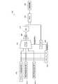
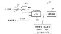
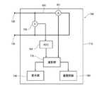
上記実施の形態に係る電流センサは、誘導磁場の大きさに応じて、異なる磁場感度を有する複数の磁気抵抗素子から最適な磁気抵抗素子を選択し、その出力電圧から選択出力信号を算出する。しかしながら、複数の磁気抵抗素子はそれぞれ磁場感度が異なるため、同一の出力電圧によって駆動していたとしても、測定した誘導磁界の値が異なる。そのため、どの磁気抵抗素子から出力された出力電圧が適切であるかを特定できなければ、被測定電流からの誘導磁場値を測定することができない。  The current sensor according to the above embodiment selects an optimum magnetoresistive element from a plurality of magnetoresistive elements having different magnetic field sensitivities according to the magnitude of the induced magnetic field, and calculates a selected output signal from the output voltage. However, since the plurality of magnetoresistive elements have different magnetic field sensitivities, even if they are driven by the same output voltage, the measured values of the induced magnetic field are different. Therefore, unless it is possible to specify which magnetoresistive element is suitable for the output voltage, it is impossible to measure the induced magnetic field value from the current to be measured.

そこで、本実施の形態に係る電流センサ600においては、n個配置された測定用磁気抵抗素子610−1〜610−nの出力信号と一つのリファレンス磁気抵抗素子620の出力信号をすべてマルチプレクサ650に入力し、所定の制御信号Scに基づいて最適な出力信号を選択する。尚、制御信号Scは、リファレンス磁気抵抗素子620の出力信号に応じて生成される。また、本実施の形態に係る電流センサ600は、直流電流を測定する。  Therefore, in thecurrent sensor 600 according to the present embodiment, all the output signals of the n measuring magnetoresistive elements 610-1 to 610-n and the output signal of onereference magnetoresistive element 620 are sent to themultiplexer 650. An optimum output signal is selected based on a predetermined control signal Sc. The control signal Sc is generated according to the output signal of thereference magnetoresistive element 620. Moreover, thecurrent sensor 600 according to the present embodiment measures a direct current.

図24に示す通り、本実施の形態に係る電流センサ600は、n個の測定用磁気抵抗素子610−1〜610−nと、リファレンス磁気抵抗素子620と、コンパレータ630と、レジスタ640と、マルチプレクサ650と、増幅器660と、A/D変換回路670と、メモリ680と、通信回路690とを備える。  As shown in FIG. 24, thecurrent sensor 600 according to the present embodiment includes n measuring magnetoresistive elements 610-1 to 610-n, areference magnetoresistive element 620, acomparator 630, aregister 640, and a multiplexer. 650, anamplifier 660, an A /D conversion circuit 670, amemory 680, and acommunication circuit 690.

n個の測定用磁気抵抗素子610−1〜610−nとリファレンス磁気抵抗効果素子は、n+1通りの異なる磁場感度を有する。測定用磁気抵抗素子610−1〜610−nとリファレンス磁気抵抗素子620は、第1及び第2の実施の形態のいずれかに係る磁気抵抗素子等を適用することが可能である。また、測定用磁気抵抗素子610−1〜610−nの近傍には、線形応答磁性体160や磁束ガイド170等を設けることも可能である。  The n measuring magnetoresistive elements 610-1 to 610-n and the reference magnetoresistive element have n + 1 different magnetic field sensitivities. As the magnetoresistive elements for measurement 610-1 to 610-n and thereference magnetoresistive element 620, the magnetoresistive elements according to any of the first and second embodiments can be applied. In addition, a linear responsemagnetic body 160, amagnetic flux guide 170, and the like can be provided in the vicinity of the measurement magnetoresistance elements 610-1 to 610-n.

リファレンス磁気抵抗素子620は、誘導磁場の大まかな大きさを測定する磁気抵抗素子であり、リファレンス磁気抵抗素子620の出力信号は、コンパレータ630による制御信号Scの生成に用いられる。従って、リファレンス磁気抵抗素子620は、n個の測定用磁気抵抗素子610−1〜610−nと比較して広い磁場範囲に感度を有する。また、リファレンス磁気抵抗素子620として、第1及び第2の実施の形態のいずれかに係る磁気抵抗素子を採用することも可能である。また、リファレンス磁気抵抗素子620の近傍に線形応答磁性体160や磁束ガイド170等を設けることも可能である。  Thereference magnetoresistive element 620 is a magnetoresistive element that measures the approximate magnitude of the induced magnetic field, and the output signal of thereference magnetoresistive element 620 is used for generation of the control signal Sc by thecomparator 630. Therefore, thereference magnetoresistive element 620 has sensitivity in a wider magnetic field range than the n measuring magnetoresistive elements 610-1 to 610-n. In addition, as thereference magnetoresistive element 620, the magnetoresistive element according to any of the first and second embodiments can be adopted. It is also possible to provide a linear responsemagnetic body 160, amagnetic flux guide 170, etc. in the vicinity of thereference magnetoresistive element 620.

コンパレータ630は、リファレンス磁気抵抗素子620の出力信号に基づいて、誘導磁場の大まかな大きさを示す制御信号Scを生成する。図25は、コンパレータ630の構成を示す回路図である。コンパレータ630は、n+1個の比較器631−1〜631−n+1を備える。比較器631−1〜631−n+1は、リファレンス磁気抵抗素子620の出力信号を基準電圧V…V,Vmax(本実施の形態に係る磁気抵抗素子のフリー層(第1磁性層101等)とピン層(第2磁性層102等)の磁化ベクトルが180°方向に向いた状態の出力電圧)と比較してその結果を出力する。従って、比較器631−1〜631−n+1の一方の入力端子はそれぞれリファレンス磁気抵抗素子620に接続されている。また、他方の入力端子にはそれぞれ異なる基準電圧V…Vn,maxが印加されている。更に、これら複数の比較器631の出力端子はレジスタ640に接続されている。尚、制御信号Scは、比較器631−1〜631−n+1の出力信号からなるn+1bitのデータ列である。Thecomparator 630 generates a control signal Sc indicating the approximate magnitude of the induced magnetic field based on the output signal of thereference magnetoresistive element 620. FIG. 25 is a circuit diagram illustrating a configuration of thecomparator 630. Thecomparator 630 includes n + 1 comparators 631-1 to 631-n + 1. The comparators 631-1 to 631-n + 1 output the output signal of thereference magnetoresistive element 620 to the reference voltages V1 ... Vn , Vmax (the free layer of the magnetoresistive element according to the present embodiment (the firstmagnetic layer 101, etc. ) And the pinned layer (secondmagnetic layer 102, etc.) with the magnetization vectors oriented in the 180 ° direction), and the result is output. Accordingly, one input terminal of each of the comparators 631-1 to 631-n + 1 is connected to thereference magnetoresistive element 620. Further, different reference voltages V1 ... Vn, Vmax are applied to the other input terminals. Further, the output terminals of the plurality ofcomparators 631 are connected to theregister 640. The control signal Sc is an n + 1 bit data string composed of output signals of the comparators 631-1 to 631-n + 1.

図24に戻って説明を続ける。レジスタ640は、コンパレータ630の出力信号を制御信号Scとして保持する。マルチプレクサ650は、この制御信号Scに基づいて測定用磁気抵抗素子610−1〜610−n、リファレンス磁気抵抗素子620の出力信号から一の出力信号を選択する。換言すれば、マルチプレクサ650は、リファレンス磁気抵抗素子620の出力電圧に基づいて測定用磁気抵抗素子610−1〜610−n、リファレンス磁気抵抗素子620を選択する。増幅器660はマルチプレクサ650の出力信号を増幅し、A/D変換回路670は増幅器660の出力信号をデジタル出力値に変換する。メモリ680はA/D変換回路670の出力信号及びレジスタ640の出力信号を格納し、通信回路690はメモリ680に格納された信号を外部に出力する。  Returning to FIG. 24, the description will be continued. Theregister 640 holds the output signal of thecomparator 630 as the control signal Sc. Themultiplexer 650 selects one output signal from the output signals of the measurement magnetoresistive elements 610-1 to 610-n and thereference magnetoresistive element 620 based on the control signal Sc. In other words, themultiplexer 650 selects the measurement magnetoresistive elements 610-1 to 610-n and thereference magnetoresistive element 620 based on the output voltage of thereference magnetoresistive element 620. Theamplifier 660 amplifies the output signal of themultiplexer 650, and the A /D conversion circuit 670 converts the output signal of theamplifier 660 into a digital output value. Thememory 680 stores the output signal of the A /D conversion circuit 670 and the output signal of theregister 640, and thecommunication circuit 690 outputs the signal stored in thememory 680 to the outside.

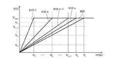
図26は、複数の測定用磁気抵抗素子610−1〜610−n及びリファレンス磁気抵抗素子620の特性を示すグラフである。横軸は誘導磁場の大きさを表しており、縦軸は測定用磁気抵抗素子610−1〜610−n及びリファレンス磁気抵抗素子620の出力電圧を表している。  FIG. 26 is a graph showing characteristics of a plurality of measurement magnetoresistive elements 610-1 to 610-n and thereference magnetoresistive element 620. The horizontal axis represents the magnitude of the induced magnetic field, and the vertical axis represents the output voltages of the measurement magnetoresistive elements 610-1 to 610-n and thereference magnetoresistive element 620.

図に示すように、複数の測定用磁気抵抗素子610−1〜610−nは、それぞれ異なる磁場感度及び異なる飽和磁場H〜Hを有する。即ち、kを1以上n以下の整数とすると、測定用磁気抵抗素子610−kは、k番目に高い磁場感度と、k番目に小さい飽和磁場Hを有する。また、リファレンス磁気抵抗素子620の磁場感度は測定用磁気抵抗素子610−nよりも低く、飽和磁場Hは測定用磁気抵抗素子610−nよりも大きい。As shown in the drawing, the plurality of measurement magnetoresistive elements 610-1 to 610-n have different magnetic field sensitivities and different saturation magnetic fields H1 to Hn , respectively. That is, if an integer from 1 to n and k, the magnetoresistive element 610-k for measurement has a high magnetic field sensitivity k-th, a small saturation magnetic field Hk in the k-th. The magnetic field sensitivity of thereference magnetoresistive element 620 is lower than that of the measuring magnetoresistive element 610-n, and the saturation magnetic fieldHr is larger than that of the measuring magnetoresistive element 610-n.

高い磁場感度を有する測定用磁気抵抗素子610−1の抵抗値は、磁場変化に対して急峻に変化し、比較的小さい磁場Hが印加された時点で磁化状態が飽和する。従って、微小な磁場を高精度に測定することが可能である。一方、低い磁場感度を有するリファレンス磁気抵抗素子620の抵抗値は、磁場変化に対してなだらかに変化し、比較的大きい磁場Hが印加されるまで磁化状態が飽和しない。従って、比較的広いダイナミックレンジにおいて磁場を測定することが可能である。The resistance of the measuring magnetoresistance element 610-1 having high magnetic field sensitivity, steeply changes with respect to the magnetic field change, and saturation magnetization at the time when a relatively small magnetic field H1 is applied. Therefore, it is possible to measure a minute magnetic field with high accuracy. On the other hand, the resistance value of thereference magnetoresistive element 620 having a low magnetic field sensitivity changes gently with respect to the magnetic field change, and the magnetization state is not saturated until a relatively large magnetic fieldHr is applied. Therefore, it is possible to measure the magnetic field in a relatively wide dynamic range.

測定用磁気抵抗素子610−1〜610−nの磁場感度の設定は、例えば次のように行う事が考えられる。先ず、要求される分解能に応じて、最も高い磁場感度を有する測定用磁気抵抗素子610−1の磁場感度を設定する。次に、要求されるダイナミックレンジに応じて、最も低い、即ち、磁場変化に対する抵抗値の変化が少ないリファレンス磁気抵抗素子620の磁場感度を設定する。更に、測定用磁気抵抗素子610−2〜610−nの磁場感度を設定する。  The magnetic field sensitivity of the measurement magnetoresistive elements 610-1 to 610-n can be set as follows, for example. First, the magnetic field sensitivity of the measuring magnetoresistive element 610-1 having the highest magnetic field sensitivity is set according to the required resolution. Next, in accordance with the required dynamic range, the magnetic field sensitivity of thereference magnetoresistive element 620 that is the lowest, that is, the resistance value change with respect to the magnetic field change is small is set. Furthermore, the magnetic field sensitivity of the magnetoresistive elements for measurement 610-2 to 610-n is set.

図26中のV〜V及びVmaxは、リファレンス磁気抵抗素子620の出力電圧と比較される上記基準電圧である。本実施の形態において、基準電圧V〜Vは、全ての測定用磁気抵抗素子610−1〜610−nについてそれぞれ1つ設定される。測定用磁気抵抗素子610−kに対応する基準電圧V(k=1〜n)は、測定用磁気抵抗素子610−kの飽和磁場Hにおける、リファレンス磁気抵抗素子620の出力電圧である。In FIG. 26, V1 to Vn and Vmax are the reference voltages that are compared with the output voltage of thereference magnetoresistive element 620. In the present embodiment,one reference voltage V1 to Vn is set for each of the measurement magnetoresistive elements 610-1 to 610 -n. Measuring the magnetoresistance element 610-k to the corresponding reference voltageV k (k =1~n) is in the saturation magnetic fieldH k of the measurement the magnetoresistive element 610-k, which is the output voltage of thereference magnetoresistive element 620.

但し、実際には、誘導磁場が飽和磁場に近付くと、誘導磁場と磁気抵抗素子の抵抗値との線形成が劣化する。従って、測定用磁気抵抗素子610−kに対応する基準電圧Vを、測定用磁気抵抗素子610−kの飽和磁場Hよりも低い磁場におけるリファレンス磁気抵抗素子620の出力電圧としても良い。同様に、Vmaxは、第1磁性層と第2磁性層の磁化ベクトルが180°方向に向き切る前の状態の磁気抵抗素子の出力電圧とすることも可能である。However, in practice, when the induction magnetic field approaches the saturation magnetic field, the line formation between the induction magnetic field and the resistance value of the magnetoresistive element deteriorates. Therefore, the reference voltage Vk corresponding to the measuring magnetoresistive element 610-k may be used as the output voltage of thereference magnetoresistive element 620 in a magnetic field lower than the saturation magnetic field Hk of the measuring magnetoresistive element 610-k. Similarly, Vmax may be the output voltage of the magnetoresistive element in a state before the magnetization vectors of the first magnetic layer and the second magnetic layer are turned in the 180 ° direction.

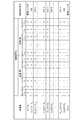
図27は、誘導磁場の大きさ、制御信号Scの値及びマルチプレクサ650によって選択される測定用磁気抵抗素子610−1〜610−n又はリファレンス磁気抵抗素子620の関係を示す表である。図27の左欄には誘導磁場の大きさを、中欄には制御信号Scを、右欄には選択される磁気抵抗素子を示している。尚、制御信号Scはn+1個の比較器631−1〜631−n+1(図25)の出力信号からなるため、図27においては、比較器631−1〜631−n+1の出力信号毎のデータを記載している。  FIG. 27 is a table showing the relationship between the magnitude of the induced magnetic field, the value of the control signal Sc, and the measurement magnetoresistive elements 610-1 to 610-n or thereference magnetoresistive element 620 selected by themultiplexer 650. The left column of FIG. 27 shows the magnitude of the induced magnetic field, the middle column shows the control signal Sc, and the right column shows the selected magnetoresistive element. Since the control signal Sc is composed of output signals of n + 1 comparators 631-1 to 631-n + 1 (FIG. 25), the data for each output signal of the comparators 631-1 to 631-n + 1 is shown in FIG. It is described.

誘導磁場の大きさHが、Hk−1≦H<Hであった場合、リファレンス磁気抵抗素子620の出力電圧は、Vk−1以上であり、Vより小さい。従って、比較器631−1〜631−k−1の出力信号は1(High)となり、比較器631−k〜631−nの出力信号は0(low)となる。これらの出力信号からなる制御信号Scを受けて、コンパレータ630は測定用磁気抵抗素子610−kの出力信号を選択し、出力する。When the magnitude H of the induced magnetic field is Hk−1 ≦ H <Hk , the output voltage of thereference magnetoresistive element 620 is equal to or higher than Vk−1 and smaller than Vk . Therefore, the output signals of the comparators 631-1 to 631-k-1 are 1 (High), and the output signals of the comparators 631-k to 631-n are 0 (low). Receiving the control signal Sc composed of these output signals, thecomparator 630 selects and outputs the output signal of the measuring magnetoresistive element 610-k.

次に、メモリ680の動作について説明する。図28は、メモリ680の動作を説明するための回路ブロック図である。マルチプレクサ650から出力された出力信号は、A/D変換回路670によってNbitのデジタルデータに変換される。また、制御信号Scはn+1bitのデジタルデータである。本実施の形態に係る電流センサ600は、制御信号Scによって選択した測定用磁気抵抗素子610を特定する。従って、メモリ680は、N+n+1bitのデジタルデータを1ユニットとして格納する。  Next, the operation of thememory 680 will be described. FIG. 28 is a circuit block diagram for explaining the operation of thememory 680. The output signal output from themultiplexer 650 is converted into N-bit digital data by the A /D conversion circuit 670. The control signal Sc is n + 1 bit digital data. Thecurrent sensor 600 according to the present embodiment specifies themeasurement magnetoresistive element 610 selected by the control signal Sc. Therefore, thememory 680 stores N + n + 1 bit digital data as one unit.

[4.第4の実施の形態]
次に、第4の実施の形態に係る電流センサ601について説明する。第3の実施に係る電流センサ600が直流電流を測定していたのに対し、第4の実施に係る電流センサ601は交流電流を測定する。本実施の形態に係る電流センサ601は、基本的には第3の実施の形態に係る電流センサ600と同様に構成されているが、コンパレータ639の構成において第3の実施の形態と異なる。以下、第3の実施の形態と同様である部分については、説明を省略する。
[4. Fourth Embodiment]
Next, acurrent sensor 601 according to the fourth embodiment will be described. Thecurrent sensor 600 according to the third implementation measures a direct current, whereas thecurrent sensor 601 according to the fourth implementation measures an alternating current. Thecurrent sensor 601 according to the present embodiment is basically configured in the same manner as thecurrent sensor 600 according to the third embodiment, but differs in the configuration of thecomparator 639 from the third embodiment. Hereinafter, description of the same parts as those of the third embodiment will be omitted.

図29は、本実施の形態に係るコンパレータ639の構成を示す回路図である。本実施の形態に係る電流センサ601は交流電流を測定するため、誘導磁場が正の値のみならず負の値にもなり得る。従って、本実施の形態に係るコンパレータ639は、2n個の比較器631−1〜631−(2n+2)を備える。比較器631−1〜631−(2n+2)は、リファレンス磁気抵抗素子620の出力信号を基準電圧Vmin(本実施の形態に係る磁気抵抗素子のフリー層(第1磁性層101等)とピン層(第2磁性層102等)の磁化ベクトルが0°方向に向いた状態の出力電圧),V…V2n,Vmaxと比較してその結果を出力する。従って、比較器631−1〜631−(2n+2)の一方の入力端子はそれぞれリファレンス磁気抵抗素子620に接続されている。また、他方の入力端子にはそれぞれ異なる基準電圧Vmin,V…V2n,Vmaxが印加されている。更に、これら複数の比較器631−1〜631−(2n+2)の出力端子はレジスタ640に接続されている。尚、本実施の形態において、制御信号Scは、比較器631−1〜631−(2n+2)の出力信号からなる2n+2bitのデータ列である。FIG. 29 is a circuit diagram showing a configuration of acomparator 639 according to the present embodiment. Since thecurrent sensor 601 according to the present embodiment measures an alternating current, the induced magnetic field can be a positive value as well as a negative value. Therefore, thecomparator 639 according to the present embodiment includes 2n comparators 631-1 to 631- (2n + 2). The comparators 631-1 to 631- (2n + 2) output the output signal of thereference magnetoresistive element 620 to the reference voltage Vmin (the free layer (firstmagnetic layer 101 etc.) and pinned layer of the magnetoresistive element according to the present embodiment). (Output voltage in a state where the magnetization vector of the secondmagnetic layer 102 etc. is oriented in the 0 ° direction), V1 ... V2n , Vmax and the result is output. Accordingly, one input terminal of each of the comparators 631-1 to 631- (2n + 2) is connected to thereference magnetoresistive element 620. Further, different reference voltages Vmin , V1 ... V2n , Vmax are applied to the other input terminals. Further, the output terminals of the plurality of comparators 631-1 to 631- (2n + 2) are connected to theregister 640. In the present embodiment, the control signal Sc is a 2n + 2 bit data string composed of the output signals of the comparators 631-1 to 631- (2n + 2).

図30は、複数の測定用磁気抵抗素子610−1〜610−n及びリファレンス磁気抵抗素子620の特性を示すグラフである。横軸は誘導磁場の大きさを表しており、縦軸は測定用磁気抵抗素子610−1〜610−n及びリファレンス磁気抵抗素子620の出力電圧を表している。  FIG. 30 is a graph showing characteristics of the plurality of magnetoresistive elements for measurement 610-1 to 610-n and thereference magnetoresistive element 620. The horizontal axis represents the magnitude of the induced magnetic field, and the vertical axis represents the output voltages of the measurement magnetoresistive elements 610-1 to 610-n and thereference magnetoresistive element 620.

図30中のVmin,V〜V2n,Vmaxは、リファレンス磁気抵抗素子620の出力電圧と比較される上記基準電圧である。本実施の形態において、基準電圧V〜V2nは、全ての測定用磁気抵抗素子610−1〜610−nについてそれぞれ2つ設定される。測定用磁気抵抗素子610−k(k=1〜n)に対応する基準電圧Vn+k及びVn−k+1は、それぞれ測定用磁気抵抗素子610−kの飽和磁場H及び−Hにおける、リファレンス磁気抵抗素子620の出力電圧である。In FIG. 30, Vmin , V1 to V2n , and Vmax are the reference voltages that are compared with the output voltage of thereference magnetoresistive element 620. In the present embodiment, two reference voltages V1 to V2n are set for each of the measurement magnetoresistive elements 610-1 to 610 -n. The reference voltages Vn + k and Vn−k + 1 corresponding to the measurement magnetoresistive element 610-k (k = 1 to n) are the reference in the saturation magnetic field Hk and −Hk of the measurement magnetoresistive element 610-k, respectively. This is the output voltage of themagnetoresistive element 620.

図31は、誘導磁場の大きさ、制御信号Scの値及びマルチプレクサ650によって選択される測定用磁気抵抗素子610−1〜610−n又はリファレンス磁気抵抗素子620の関係を示す表である。図31の左欄には誘導磁場の大きさを、中欄には制御信号Scを、右欄には選択される磁気抵抗素子を示している。尚、制御信号Scは2n+2個の比較器631−1〜631−(2n+2)(図29)の出力信号からなるため、図31においては、比較器631−1〜631−(2n+2)の出力信号毎のデータを記載している。  FIG. 31 is a table showing the relationship between the magnitude of the induced magnetic field, the value of the control signal Sc, and the measurement magnetoresistive elements 610-1 to 610-n or thereference magnetoresistive element 620 selected by themultiplexer 650. The left column of FIG. 31 shows the magnitude of the induced magnetic field, the middle column shows the control signal Sc, and the right column shows the selected magnetoresistive element. Since the control signal Sc is composed of output signals of 2n + 2 comparators 631-1 to 631- (2n + 2) (FIG. 29), the output signals of the comparators 631-1 to 631- (2n + 2) are shown in FIG. Each data is described.

誘導磁場の大きさHが負の値であり、−H≦H<−Hk−1であった場合、リファレンス磁気抵抗素子620の出力電圧は、Vn−k+1以上であり、Vn−kより小さい。従って、比較器631−1〜631−(n−k+1)の出力信号は1(High)となり、比較器631−(n−k)〜631−2nの出力信号は0(low)となる。一方、誘導磁場の大きさHが正の値であり、Hk−1≦H<Hであった場合、リファレンス磁気抵抗素子620の出力電圧は、Vn+k−1以上であり、Vn+kより小さい。従って、比較器631−1〜631−(k−1)の出力信号は1(High)となり、比較器631−k〜631−nの出力信号は0(low)となる。これらの出力信号からなる制御信号Scを受けて、コンパレータ639は測定用磁気抵抗素子610−kの出力信号を選択し、出力する。When the magnitude H of the induced magnetic field is a negative value and −Hk ≦ H <−Hk−1 , the output voltage of thereference magnetoresistive element 620 is Vn−k + 1 or more, and Vn− less thank . Therefore, the output signals of the comparators 631-1 to 631- (n−k + 1) are 1 (High), and the output signals of the comparators 631- (n−k) to 631-2n are 0 (low). On the other hand, when the magnitude H of the induced magnetic field is a positive value and Hk−1 ≦ H <Hk , the output voltage of thereference magnetoresistive element 620 is equal to or higher than Vn + k−1 and from Vn + k small. Therefore, the output signals of the comparators 631-1 to 631- (k-1) are 1 (High), and the output signals of the comparators 631-k to 631-n are 0 (low). Receiving the control signal Sc composed of these output signals, thecomparator 639 selects and outputs the output signal of the measuring magnetoresistive element 610-k.

次に、メモリ680の動作について説明する。図32は、メモリ680の動作を説明するための回路ブロック図である。マルチプレクサ650から出力された出力信号は、A/D変換回路670によってNbitのデジタルデータに変換される。また、制御信号Scは2n+2bitのデジタルデータである。本実施の形態に係る電流センサ600は、制御信号Scによって選択した測定用磁気抵抗素子610を特定する。従って、メモリ680は、N+2n+2bitのデジタルデータを1ユニットとして格納する。  Next, the operation of thememory 680 will be described. FIG. 32 is a circuit block diagram for explaining the operation of thememory 680. The output signal output from themultiplexer 650 is converted into N-bit digital data by the A /D conversion circuit 670. The control signal Sc is 2n + 2 bit digital data. Thecurrent sensor 600 according to the present embodiment specifies themeasurement magnetoresistive element 610 selected by the control signal Sc. Therefore, thememory 680 stores N + 2n + 2 bit digital data as one unit.

尚、上記測定用磁気抵抗素子610_1〜610_n及びリファレンス磁気抵抗素子620としては、複数の第1の磁気抵抗素子100又は第2の磁気抵抗素子200を直列又は並列に接続した物を用いることも可能である。図33は、このような実施の形態に係る電流センサを例示する模式図である。  As the measurement magnetoresistive elements 610_1 to 610_n and thereference magnetoresistive element 620, it is possible to use a plurality of firstmagnetoresistive elements 100 or secondmagnetoresistive elements 200 connected in series or in parallel. It is. FIG. 33 is a schematic view illustrating a current sensor according to such an embodiment.

図33(a)に表したように、例えば複数の第1の磁気抵抗素子100を電気的に直列に接続して測定用磁気抵抗素子610_k(k=1〜n−1)とし、複数の第2の磁気抵抗素子200を電気的に直列に接続して測定用磁気抵抗素子610_k+1としてもよい。直列に接続されている磁気抵抗素子の数をNとしたとき、得られる電気信号は、磁気抵抗素子の数が1である場合のN倍となる。その一方で、熱ノイズ及びショットキーノイズは、N1/2倍になる。すなわち、SN比(signal-noise ratio:SNR)は、N1/2倍になる。直列に接続する磁気抵抗素子の数Nを増やすことで、SN比を改善することができる。As shown in FIG. 33A, for example, a plurality of firstmagnetoresistive elements 100 are electrically connected in series to form a measuring magnetoresistive element 610_k (k = 1 to n−1). Twomagnetoresistive elements 200 may be electrically connected in series to form a measuringmagnetoresistive element 610 — k + 1. When the number of magnetoresistive elements connected in series is N, the obtained electric signal is N times that when the number of magnetoresistive elements is 1. On the other hand, thermal noise and Schottky noise are N1/2 times. That is, the SN ratio (signal-noise ratio: SNR) is N1/2 times. The SN ratio can be improved by increasing the number N of magnetoresistive elements connected in series.

1つの磁気抵抗素子に加えられるバイアス電圧は、例えば、50ミリボルト(mV)以上150mV以下である。N個の磁気抵抗素子を直列に接続した場合は、バイアス電圧は、50mV×N以上150mV×N以下となる。例えば、直列に接続されている磁気抵抗素子の数Nが25である場合には、バイアス電圧は、1V以上3.75V以下となる。  The bias voltage applied to one magnetoresistive element is, for example, 50 millivolts (mV) or more and 150 mV or less. When N magnetoresistive elements are connected in series, the bias voltage is 50 mV × N or more and 150 mV × N or less. For example, when the number N of magnetoresistive elements connected in series is 25, the bias voltage is 1 V or more and 3.75 V or less.

バイアス電圧の値が1V以上であると、磁気抵抗素子から得られる電気信号を処理する電気回路の設計は容易になり、実用的に好ましい。  When the value of the bias voltage is 1 V or more, the design of an electric circuit for processing an electric signal obtained from the magnetoresistive element becomes easy, which is practically preferable.

バイアス電圧(端子間電圧)が10Vを超えると、磁気抵抗素子から得られる電気信号を処理する電気回路においては、望ましくない。実施形態においては、適切な電圧範囲になるように、直列に接続される磁気抵抗素子の数N及びバイアス電圧が設定される。  When the bias voltage (inter-terminal voltage) exceeds 10 V, it is not desirable in an electric circuit that processes an electric signal obtained from the magnetoresistive element. In the embodiment, the number N of magnetoresistive elements connected in series and the bias voltage are set so as to be in an appropriate voltage range.

例えば、複数の磁気抵抗素子を電気的に直列に接続したときの電圧は、1V以上10V以下となるのが好ましい。例えば、電気的に直列に接続された複数の磁気抵抗素子の端子間(一方の端の端子と、他方の端の端子と、の間)に印加される電圧は、1V以上10V以下である。  For example, the voltage when a plurality of magnetoresistive elements are electrically connected in series is preferably 1 V or more and 10 V or less. For example, a voltage applied between terminals of a plurality of magnetoresistive elements electrically connected in series (between one terminal and the other terminal) is 1 V or more and 10 V or less.

図33(b)に表したように、他の実施の形態に係る電流センサにおいては、例えば複数の第1の磁気抵抗素子100を電気的に並列に接続して測定用磁気抵抗素子610_k(k=1〜n)とし、複数の第2の磁気抵抗素子200を電気的に並列に接続して測定用磁気抵抗素子610_k+1としても良い。  As shown in FIG. 33B, in the current sensor according to another embodiment, for example, a plurality of firstmagnetoresistive elements 100 are electrically connected in parallel to measure the magnetoresistive element 610_k (k = 1 to n), and the plurality of secondmagnetoresistive elements 200 may be electrically connected in parallel to form the measuring magnetoresistiveelement 610_k + 1.

図33(c)に表したように、他の実施の形態に係る電流センサにおいては、例えば複数の第1の磁気抵抗素子100と第1の磁気抵抗素子の逆極性を示す抵抗値が同一の磁気抵抗素子110を、ホイートストンブリッジ回路を形成するように接続して測定用磁気抵抗素子610_k(k=1〜n)とし、複数の第2の磁気抵抗素子200と第2の磁気抵抗素子の逆極性を示す抵抗値が同一の磁気抵抗素子210を、ホイートストンブリッジ回路を形成するように接続して測定用磁気抵抗素子610_k+1としても良い。これにより、例えば、検出特性の温度補償を行うことができる。  As shown in FIG. 33C, in the current sensor according to another embodiment, for example, the resistance values indicating the reverse polarities of the plurality of firstmagnetoresistive elements 100 and the first magnetoresistive elements are the same. Themagnetoresistive element 110 is connected so as to form a Wheatstone bridge circuit to be a measurement magnetoresistive element 610_k (k = 1 to n), and the plurality of secondmagnetoresistive elements 200 and the reverse of the second magnetoresistive elements. Themagnetoresistive elements 210 having the same resistance value indicating polarity may be connected to form a Wheatstone bridge circuit to form the measuring magnetoresistiveelement 610_k + 1. Thereby, for example, temperature compensation of detection characteristics can be performed.

また、前述の磁気抵抗素子110に代えて第1の磁気抵抗素子100と同一抵抗値の固定抵抗を採用し、前述の磁気抵抗素子210に代えて第2の磁気抵抗素子200と同一抵抗値の固定抵抗を採用しても良い(ハーフホイーストンブリッジ回路)。  Further, a fixed resistor having the same resistance value as that of the firstmagnetoresistive element 100 is employed instead of theaforementioned magnetoresistive element 110, and the same resistance value as that of thesecond magnetoresistive element 200 is employed instead of theaforementioned magnetoresistive element 210. A fixed resistor may be used (half Wheatstone bridge circuit).

図33(d)に表したように、他の実施の形態に係る電流センサにおいては、例えば複数の第1の磁気抵抗素子100を直列に接続した磁気抵抗素子120と前記磁気抵抗素子110を直列に接続した130によってホイートストンブリッジ回路を形成し、このホイートストンブリッジ回路を測定用磁気抵抗素子610_k(k=1〜n)としても良い。また、例えば複数の第2の磁気抵抗素子200を直列に接続した磁気抵抗素子220と、前記磁気抵抗素子210を直列に接続した磁気抵抗素子230によってホイートストンブリッジ回路を形成し、このホイートストンブリッジ回路を測定用磁気抵抗素子610_k+1としても良い。  As shown in FIG. 33D, in a current sensor according to another embodiment, for example, amagnetoresistive element 120 in which a plurality of firstmagnetoresistive elements 100 are connected in series and themagnetoresistive element 110 are connected in series. A Wheatstone bridge circuit may be formed by 130 connected to the magnetic resistance element 610_k (k = 1 to n) for measurement. For example, a Wheatstone bridge circuit is formed by amagnetoresistive element 220 in which a plurality of secondmagnetoresistive elements 200 are connected in series and amagnetoresistive element 230 in which themagnetoresistive elements 210 are connected in series. The magnetoresistive element formeasurement 610_k + 1 may be used.

また、前述の磁気抵抗素子130に代えて磁気抵抗素子120と同一の抵抗値の固定抵抗を採用し、前述の磁気抵抗素子230に代えて磁気抵抗素子220と同一の抵抗値の固定抵抗を採用しても良い(ハーフホイーストンブリッジ回路)。  Further, a fixed resistor having the same resistance value as that of themagnetoresistive element 120 is employed instead of the above-describedmagnetoresistive element 130, and a fixed resistor having the same resistance value as that of themagnetoresistive element 220 is employed instead of the above-describedmagnetoresistive element 230. Yes (half Wheatstone bridge circuit).

[5.第5の実施の形態]
次に、第5の実施の形態について説明する。本実施の形態においては、上記第1〜第4の実施の形態に係る電流センサをスマートメータに搭載している。スマートメータは電圧及び電流を測定する。ここで、電圧は従来の半導体素子において測定することが可能である。従って、上記実施の形態のいずれかに係る電流センサにこの半導体素子を付加することで、スマートメータを構成することが可能である。以下においては、第4の実施の形態に係る電流センサ601をスマートメータに適用した例について説明するが、他の実施の形態に係る電流センサを適用することも可能である。
[5. Fifth embodiment]
Next, a fifth embodiment will be described. In the present embodiment, the current sensor according to the first to fourth embodiments is mounted on a smart meter. Smart meters measure voltage and current. Here, the voltage can be measured in a conventional semiconductor element. Therefore, it is possible to configure a smart meter by adding this semiconductor element to the current sensor according to any of the above embodiments. In the following, an example in which thecurrent sensor 601 according to the fourth embodiment is applied to a smart meter will be described, but a current sensor according to another embodiment can also be applied.

図34(a)は、本実施の形態に係るスマートメータ700の外観を示す模式的な斜視図、図34(b)は、同スマートメータ700の模式的な平面図、図34(c)は、同スマートメータ700の模式的な側面図である。  34A is a schematic perspective view showing the appearance of thesmart meter 700 according to the present embodiment, FIG. 34B is a schematic plan view of thesmart meter 700, and FIG. 2 is a schematic side view of thesmart meter 700. FIG.

図34(a)〜(c)に示す通り、スマートメータ700は、センサ部を納めるための筐体710、並びに、筐体710に設けられた第1の端子部720、第2の端子部730及び電力量を外部に表示する表示部740を備える。筐体710は、本実施の形態に係るスマートメータ700の各構成を格納する。第1の端子部720及び第2の端子部730は、図示しないプローブを介してスマートメータ700の各構成と、被測定対象とを電気的に接続する。表示部740は、スマートメータ700による測定の結果等を表示する。尚、筐体710に収容されるスマートメータの各構成を電流測定モジュールと呼ぶ。  As shown in FIGS. 34A to 34C, thesmart meter 700 includes ahousing 710 for housing the sensor unit, and a firstterminal unit 720 and a secondterminal unit 730 provided in thehousing 710. And adisplay unit 740 for displaying the amount of power to the outside.Case 710 stores each component ofsmart meter 700 according to the present embodiment. The firstterminal portion 720 and the secondterminal portion 730 electrically connect each component of thesmart meter 700 and the measurement target via a probe (not shown). Thedisplay unit 740 displays the result of measurement by thesmart meter 700 and the like. Each configuration of the smart meter housed in thehousing 710 is referred to as a current measurement module.

本実施の形態に係るスマートメータ700は、例えば50〜60Hz程度の交流電流及び交流電圧を計測することが可能である様に構成することが考えられるが、例えば直流電流及び直流電圧のみを計測可能な構成としても良い。また、図34においては、100〜200V程度の単層交流の電流及び電圧を測定可能である例を示しているが、例えば三相交流の電流及び電圧を測定可能に構成しても良い。この場合、上記端子部720及び730は、3対設けられる。  Thesmart meter 700 according to the present embodiment may be configured so as to be able to measure, for example, an alternating current and an alternating voltage of about 50 to 60 Hz. For example, only the direct current and the direct voltage can be measured. It is good also as a simple structure. FIG. 34 shows an example in which a single-layer AC current and voltage of about 100 to 200 V can be measured. For example, a three-phase AC current and voltage may be measured. In this case, three pairs of theterminal portions 720 and 730 are provided.

図34(b)に示す通り、スマートメータ700は、筐体710内に、配線500と、電子基板モジュール711と、電流センサ601とを収容している。配線500は、一端が第1の端子部720に、他端が第2の端子部730に接続されている。また、配線500は、筐体710の上下方向(以下、Z方向)に被測定電流を流すように配置され、絶縁性の電流線固定支持部510(図37(c))を介して筐体710に固定されている。電子基板モジュール711は、筐体710内に、筐体710の底面と平行に固定されている。電流センサ601は、電子基板モジュール711上に、筐体710の底面と平行に固定されている。従って、本実施の形態に係るスマートメータ700においては、配線500と電流センサ601の位置関係が固定されているため、被測定電流からの誘導磁場を好適に測定可能である。  As shown in FIG. 34 (b), thesmart meter 700 houses awiring 500, anelectronic board module 711, and acurrent sensor 601 in ahousing 710. Thewiring 500 has one end connected to the firstterminal portion 720 and the other end connected to the secondterminal portion 730. Further, thewiring 500 is arranged so that a current to be measured flows in the vertical direction of the casing 710 (hereinafter referred to as Z direction), and the casing is interposed via an insulating current line fixing support portion 510 (FIG. 37C). 710 is fixed. Theelectronic board module 711 is fixed in thehousing 710 in parallel with the bottom surface of thehousing 710. Thecurrent sensor 601 is fixed on theelectronic board module 711 in parallel with the bottom surface of thehousing 710. Therefore, in thesmart meter 700 according to the present embodiment, since the positional relationship between thewiring 500 and thecurrent sensor 601 is fixed, it is possible to suitably measure the induced magnetic field from the current to be measured.

図35(a)及び(b)は、同スマートメータ700の一部の構成を説明するための模式図である。図35(a)及び(b)に示す通り、本実施の形態において、被測定電流からの誘導磁場の方向は、筐体710の左右方向(以下、X方向)である。また、電流センサ601は第1の磁気抵抗素子100を備えている。第1の磁気抵抗素子100は、例えば第1の実施の形態に係る磁気抵抗素子100と同様に構成されており、第1磁性層101、第2磁性層102及び中間層103を備える。第1磁性層101の初期磁化方向(配線500に電流が流れていない時の磁化方向)は、電流センサ601から配線500に向かう方向又はその逆方向(以下、Y方向)である。これにより、交流電流のいずれの極性の電流も線形成良く検知することが可能となる。  FIGS. 35A and 35B are schematic views for explaining a partial configuration of thesmart meter 700. FIG. As shown in FIGS. 35A and 35B, in the present embodiment, the direction of the induced magnetic field from the current to be measured is the left-right direction of the casing 710 (hereinafter, the X direction). Thecurrent sensor 601 includes a firstmagnetoresistive element 100. The firstmagnetoresistive element 100 is configured similarly to themagnetoresistive element 100 according to the first embodiment, for example, and includes a firstmagnetic layer 101, a secondmagnetic layer 102, and anintermediate layer 103. The initial magnetization direction of the first magnetic layer 101 (the magnetization direction when no current flows through the wiring 500) is the direction from thecurrent sensor 601 toward thewiring 500 or the opposite direction (hereinafter referred to as the Y direction). This makes it possible to detect any polarity of alternating current with good line formation.

図35に示す構造においては、好適に磁化アライメントが行われ、外部ノイズの影響を好適に低減する事が可能である。即ち、外部磁場ノイズが最も印可されやすい電流センサ601の表面から外部磁界が印可された場合、その面(xy平面)に直行する方向(z方向)に磁界が印可される。しかしながら電流センサ601の磁化方向(第1磁性層101の磁化方向)はその面(xy平面)と平行であるため、その面と直行する方向(z方向)の磁界を印加されても、ほぼノイズを生じない。この磁化アライメントによれば、外部磁場の影響をよけいな構造を付加することなく少なくする事が可能である。尚、電流センサ601の断面方向においては、磁気シールドを設けても良い。この磁気シールドは、電流測定モジュールの中では最も断面積が小さい。従って、磁気シールドを追加することに伴うコストの増大も最小限に抑えることが可能になる。また電流センサ601の基板をそのまま電子基板モジュール711に貼り付けることが可能なので、配置の誤差による影響などが少なくなり、配置の精度を高く保つために必要な製造コストを最小限に抑えることが可能となる。よって、図34、図35に示したような構成においては、配線500による誘導磁界と電流センサ601の磁化アライメントを好適に行う事が可能である。  In the structure shown in FIG. 35, magnetization alignment is suitably performed, and the influence of external noise can be suitably reduced. That is, when an external magnetic field is applied from the surface of thecurrent sensor 601 to which external magnetic field noise is most easily applied, the magnetic field is applied in a direction (z direction) perpendicular to the surface (xy plane). However, since the magnetization direction of the current sensor 601 (the magnetization direction of the first magnetic layer 101) is parallel to the surface (xy plane), even if a magnetic field in a direction perpendicular to the surface (z direction) is applied, almost no noise is applied. Does not occur. According to this magnetization alignment, it is possible to reduce the influence of the external magnetic field without adding a special structure. A magnetic shield may be provided in the cross-sectional direction of thecurrent sensor 601. This magnetic shield has the smallest cross-sectional area among the current measurement modules. Therefore, the increase in cost associated with adding a magnetic shield can be minimized. In addition, since the substrate of thecurrent sensor 601 can be attached to theelectronic substrate module 711 as it is, the influence of an arrangement error is reduced, and the manufacturing cost necessary to keep the arrangement accuracy high can be minimized. It becomes. Therefore, in the configuration shown in FIGS. 34 and 35, it is possible to suitably perform the magnetic alignment of the induced magnetic field by thewiring 500 and thecurrent sensor 601.

さらに、図34のような配置することにより、同一基板上に複数の電流センサを配置することが可能である。そのため、製造コストの低減を図ることが可能となる。  Furthermore, by arranging as shown in FIG. 34, a plurality of current sensors can be arranged on the same substrate. For this reason, it is possible to reduce the manufacturing cost.

図36は、スマートメータ700の概略構成を示す機能ブロック図である。図36に示す通り、スマートメータ700は、上記配線500及び電流センサ601に加え、電圧計750、A/D変換回路760、演算部770及び通信回路780を更に備える。尚、電圧計750、A/D変換回路760、演算部770及び通信回路780は、半導体素子として電子基板モジュール711上に作り込む事も可能である。  FIG. 36 is a functional block diagram showing a schematic configuration of thesmart meter 700. As shown in FIG. 36, thesmart meter 700 further includes avoltmeter 750, an A /D conversion circuit 760, acalculation unit 770, and acommunication circuit 780 in addition to thewiring 500 and thecurrent sensor 601. Note that thevoltmeter 750, the A /D conversion circuit 760, thecalculation unit 770, and thecommunication circuit 780 can be built on theelectronic substrate module 711 as semiconductor elements.

電流センサ601は、第4の実施の形態に係る電流センサ601である。しかし、メモリ680や通信回路690を省略することも可能である。電流センサ601は、配線500の近傍に配置され、配線500に流れる電流を測定する。  Thecurrent sensor 601 is thecurrent sensor 601 according to the fourth embodiment. However, thememory 680 and thecommunication circuit 690 can be omitted. Thecurrent sensor 601 is disposed in the vicinity of thewiring 500 and measures a current flowing through thewiring 500.

電圧計750としては、種々の電圧計を適用することが可能である。電圧計750は、第1の端子部720及び第2の端子部730の間の電圧を測定する。A/D変換回路760は、電圧計750によって測定された電圧値をデジタル信号に変換する。  As thevoltmeter 750, various voltmeters can be applied. Thevoltmeter 750 measures the voltage between the firstterminal unit 720 and the secondterminal unit 730. The A /D conversion circuit 760 converts the voltage value measured by thevoltmeter 750 into a digital signal.

演算部770は、電流センサ601から電流値を、A/D変換回路760から電圧値を取得し、電力の算出等を行う。表示部740は、演算部から電流値、電圧値及び電力の大きさ等を取得し、表示する。通信回路780は、同じく演算部から電流値、電圧値及び電力の大きさ等を取得し、スマートメータ700の外部に出力する。  Thecalculation unit 770 acquires a current value from thecurrent sensor 601 and a voltage value from the A /D conversion circuit 760, and calculates power and the like. Thedisplay unit 740 acquires and displays the current value, voltage value, power magnitude, and the like from the calculation unit. Similarly, thecommunication circuit 780 obtains a current value, a voltage value, a magnitude of power, and the like from the arithmetic unit and outputs them to the outside of thesmart meter 700.

[6.第6の実施の形態]
次に、第6の実施の形態に係るスマートメータ701について説明する。図37(a)は、本実施の形態に係るスマートメータ701の模式的な平面図、図37(b)は、同スマートメータ701の模式的な側面図である。
[6. Sixth Embodiment]
Next, asmart meter 701 according to a sixth embodiment will be described. FIG. 37A is a schematic plan view of thesmart meter 701 according to the present embodiment, and FIG. 37B is a schematic side view of thesmart meter 701.

本実施の形態に係るスマートメータ701は、基本的には第5の実施の形態に係るスマートメータ700と同様に構成されているが、磁気抵抗素子の配置において第5の実施の形態と異なる。即ち、図37(a)及び(b)に示す通り、本実施の形態においては、複数の測定用磁気抵抗素子610が、配線500からの距離が異なる様に配置されている。また、複数の測定用磁気抵抗素子610よりも更に配線500から遠い位置に、リファレンス磁気抵抗素子620が配置されている。  Thesmart meter 701 according to the present embodiment is basically configured similarly to thesmart meter 700 according to the fifth embodiment, but differs from the fifth embodiment in the arrangement of magnetoresistive elements. That is, as shown in FIGS. 37A and 37B, in the present embodiment, the plurality of measurementmagnetoresistive elements 610 are arranged so that the distance from thewiring 500 is different. Further, areference magnetoresistive element 620 is arranged at a position farther from thewiring 500 than the plurality of measurementmagnetoresistive elements 610.

本実施の形態に係るスマートメータ701において、複数の測定用磁気抵抗素子610に印加される誘導磁場の大きさは全て異なり、配線500との距離が小さいほど強い磁場が印加される。本実施の形態に係るスマートメータ701においては、このような方法によって測定用磁気抵抗素子610の磁場感度を調整している。  In thesmart meter 701 according to the present embodiment, the magnitudes of the induction magnetic fields applied to the plurality of measurementmagnetoresistive elements 610 are all different, and a stronger magnetic field is applied as the distance from thewiring 500 is smaller. In thesmart meter 701 according to the present embodiment, the magnetic field sensitivity of themeasurement magnetoresistive element 610 is adjusted by such a method.

[7.第7の実施の形態]
次に、第7の実施の形態に係るスマートメータ702について説明する。図38は、本実施の形態に係るスマートメータ702の模式的な平面図である。
[7. Seventh Embodiment]
Next, asmart meter 702 according to a seventh embodiment will be described. FIG. 38 is a schematic plan view ofsmart meter 702 according to the present embodiment.

本実施の形態に係るスマートメータ702は、基本的には第5の実施の形態に係るスマートメータ700と同様に構成されているが、磁気抵抗素子の配置において第5の実施の形態と異なる。即ち、図38に示す通り、本実施の形態においては、複数の測定用磁気抵抗素子610及びリファレンス磁気抵抗素子620が、配線500からほぼ同程度の位置に配置されている。また、本実施の形態においては、複数の測定用磁気抵抗素子610及びリファレンス磁気抵抗素子620として第1の実施の形態に係る電流センサの磁気抵抗素子が採用されており、これらの磁場感度は、第1の実施の形態において説明した種々の線形応答磁性体によって調整されている。  Thesmart meter 702 according to the present embodiment is basically configured similarly to thesmart meter 700 according to the fifth embodiment, but differs from the fifth embodiment in the arrangement of magnetoresistive elements. That is, as shown in FIG. 38, in the present embodiment, a plurality of measurementmagnetoresistive elements 610 and referencemagnetoresistive elements 620 are arranged at approximately the same position from thewiring 500. In the present embodiment, the magnetoresistive elements of the current sensor according to the first embodiment are employed as the plurality of measurementmagnetoresistive elements 610 and thereference magnetoresistive element 620. It is adjusted by the various linear response magnetic bodies described in the first embodiment.

尚、複数の測定用磁気抵抗素子610及びリファレンス磁気抵抗素子620は、図39に示す通り、電子基板モジュール711上に、マトリクス状に配置することも可能である。磁気抵抗素子をこのように配置した場合、線形応答磁性体等による磁場感度の調整に加え、配線500との距離の違いによる磁場感度の調整を行い、更に広い範囲の誘導磁界を測定することが可能となる。  The plurality of measurementmagnetoresistive elements 610 and the referencemagnetoresistive elements 620 can also be arranged in a matrix on theelectronic substrate module 711 as shown in FIG. When the magnetoresistive element is arranged in this way, in addition to the adjustment of the magnetic field sensitivity by the linear response magnetic body or the like, the magnetic field sensitivity is adjusted by the difference in the distance from thewiring 500, and a wider range of the induced magnetic field can be measured. It becomes possible.

[8.第8の実施の形態]
次に、第8の実施の形態に係るスマートメータ703について説明する。図40(a)は、本実施の形態に係るスマートメータ703の外観を示す模式的な斜視図、図40(b)は、同スマートメータ703の模式的な平面図、図40(c)は、同スマートメータ703の模式的な側面図である。また、図41(a)及び(b)は、同スマートメータ703の一部の構成を説明するための模式図である。
[8. Eighth Embodiment]
Next, asmart meter 703 according to an eighth embodiment will be described. FIG. 40A is a schematic perspective view showing the appearance of thesmart meter 703 according to the present embodiment, FIG. 40B is a schematic plan view of thesmart meter 703, and FIG. 2 is a schematic side view of thesmart meter 703. FIG. FIGS. 41A and 41B are schematic diagrams for explaining a partial configuration of thesmart meter 703.

本実施の形態に係るスマートメータ703は、基本的には第5の実施の形態に係るスマートメータ700と同様に構成されているが、以下の点において、第5の実施の形態に係るスマートメータ700と異なる。  Thesmart meter 703 according to the present embodiment is basically configured in the same manner as thesmart meter 700 according to the fifth embodiment. However, the smart meter according to the fifth embodiment is configured in the following points. Different from 700.

即ち、図40(a)に示す通り、本実施の形態に係るスマートメータ703においては、第1の端子部720及び第2の端子部730がX方向に配設されている。また、第1の端子部720及び第2の端子部730がX方向に配設されている為、図40(b)及び(c)に示す通り、配線500は、筐体710のX方向に被測定電流を流すように配置されている。更に、この場合、被測定電流による誘導磁場の方向は筐体710のY方向となる。従って、図41(a)及び(b)に示す通り、電流センサ601は、電子基板モジュール711上に、筐体710の底面と垂直に固定されている。  That is, as shown in FIG. 40A, in thesmart meter 703 according to the present embodiment, the firstterminal portion 720 and the secondterminal portion 730 are arranged in the X direction. In addition, since the firstterminal portion 720 and the secondterminal portion 730 are arranged in the X direction, thewiring 500 is arranged in the X direction of thehousing 710 as shown in FIGS. The current to be measured is arranged to flow. Further, in this case, the direction of the induced magnetic field due to the current to be measured is the Y direction of thehousing 710. Therefore, as shown in FIGS. 41A and 41B, thecurrent sensor 601 is fixed on theelectronic board module 711 perpendicularly to the bottom surface of thehousing 710.

[9.第9の実施の形態]
次に、第9の実施の形態に係るスマートメータ704について説明する。図42(a)は、本実施の形態に係るスマートメータ704の外観を示す模式的な平面図、図42(b)は、同スマートメータ704の模式的な側面図である。
[9. Ninth Embodiment]
Next, asmart meter 704 according to a ninth embodiment will be described. FIG. 42A is a schematic plan view showing the appearance of thesmart meter 704 according to the present embodiment, and FIG. 42B is a schematic side view of thesmart meter 704.

本実施の形態に係るスマートメータ704は、基本的には第8の実施の形態に係るスマートメータ703と同様に構成されているが、磁気抵抗素子の配置において第8の実施の形態と異なる。即ち、図42(a)及び(b)に示す通り、本実施の形態においては、複数の測定用磁気抵抗素子610が、配線500との距離が異なる様に配置されている。また、複数の測定用磁気抵抗素子610よりも更に配線500から遠い位置に、リファレンス磁気抵抗素子620が配置されている。  Thesmart meter 704 according to the present embodiment is basically configured similarly to thesmart meter 703 according to the eighth embodiment, but differs from the eighth embodiment in the arrangement of the magnetoresistive elements. That is, as shown in FIGS. 42A and 42B, in the present embodiment, a plurality of measurementmagnetoresistive elements 610 are arranged such that the distance from thewiring 500 is different. Further, areference magnetoresistive element 620 is arranged at a position farther from thewiring 500 than the plurality of measurementmagnetoresistive elements 610.

本実施の形態に係るスマートメータ704において、複数の測定用磁気抵抗素子610に印加される誘導磁場の大きさは全て異なり、配線500との距離が小さいほど強い磁場が印加される。本実施の形態に係るスマートメータ704においては、このような方法によって測定用磁気抵抗素子610の磁場感度を調整している。  In thesmart meter 704 according to the present embodiment, the magnitudes of the induction magnetic fields applied to the plurality of measurementmagnetoresistive elements 610 are all different, and a stronger magnetic field is applied as the distance from thewiring 500 is smaller. In thesmart meter 704 according to the present embodiment, the magnetic field sensitivity of themeasurement magnetoresistive element 610 is adjusted by such a method.

[10.第10の実施の形態]
次に、第10の実施の形態に係るスマートメータ705について説明する。図43は、本実施の形態に係るスマートメータ705の模式的な平面図である。
[10. Tenth Embodiment]
Next, asmart meter 705 according to the tenth embodiment will be described. FIG. 43 is a schematic plan view ofsmart meter 705 according to the present embodiment.

本実施の形態に係るスマートメータ705は、基本的には第8の実施の形態に係るスマートメータ703と同様に構成されているが、磁気抵抗素子の配置において第8の実施の形態と異なる。即ち、図43に示す通り、本実施の形態においては、複数の測定用磁気抵抗素子610及びリファレンス磁気抵抗素子620が、配線500からほぼ同程度の位置に配置されている。また、本実施の形態においては、複数の測定用磁気抵抗素子610及びリファレンス磁気抵抗素子620として第1の実施の形態に係る電流センサの磁気抵抗素子が採用されており、これらの磁場感度は、第1の実施の形態において説明した種々の線形応答磁性体によって調整されている。  Thesmart meter 705 according to the present embodiment is basically configured similarly to thesmart meter 703 according to the eighth embodiment, but differs from the eighth embodiment in the arrangement of the magnetoresistive elements. That is, as shown in FIG. 43, in the present embodiment, a plurality of measurementmagnetoresistive elements 610 and referencemagnetoresistive elements 620 are arranged at approximately the same position from thewiring 500. In the present embodiment, the magnetoresistive elements of the current sensor according to the first embodiment are employed as the plurality of measurementmagnetoresistive elements 610 and thereference magnetoresistive element 620. It is adjusted by the various linear response magnetic bodies described in the first embodiment.

尚、複数の測定用磁気抵抗素子610及びリファレンス磁気抵抗素子620は、図44に示す通り、電子基板モジュール711上に、マトリクス状に配置することも可能である。磁気抵抗素子をこのように配置した場合、線形応答磁性体等による磁場感度の調整に加え、配線500との距離の違いによる磁場感度の調整を行い、更に広い範囲の誘導磁界を測定することが可能となる。  Note that the plurality of measuringmagnetoresistive elements 610 and the referencemagnetoresistive elements 620 can be arranged in a matrix on theelectronic substrate module 711 as shown in FIG. When the magnetoresistive element is arranged in this way, in addition to the adjustment of the magnetic field sensitivity by the linear response magnetic body or the like, the magnetic field sensitivity is adjusted by the difference in the distance from thewiring 500, and a wider range of the induced magnetic field can be measured. It becomes possible.

[11.第11の実施の形態]
次に、第11の実施の形態について説明する。第11の実施の形態に係る電流センサは、家庭用電化製品に搭載されている。これにより、HEMS(Home Energy Management System)を実現することも可能である。図45は、本実施の形態に係る家庭用電化製品の様子を示す模式図である。電流センサは、種々の家庭用電化製品に搭載することが可能であるが、図45においては、エアーコンディショナー800に搭載した場合の様子を示している。
[11. Eleventh embodiment]
Next, an eleventh embodiment will be described. The current sensor according to the eleventh embodiment is mounted on a household appliance. Thereby, it is also possible to realize HEMS (Home Energy Management System). FIG. 45 is a schematic diagram showing a state of the household appliance according to the present embodiment. Although the current sensor can be mounted on various household appliances, FIG. 45 shows a state where the current sensor is mounted on theair conditioner 800.

本実施の形態に係るエアーコンディショナー800は、電流測定機構801を備えている。電流測定機構801は、例えば第4の実施の形態に係る電流センサ601を筐体802中に収容してなる。筐体802の側面には第1及び第2の端子部803,804が設けられており、電流センサ601はこれら第1及び第2の端子部を介して他の部品と接続される。  Theair conditioner 800 according to the present embodiment includes acurrent measurement mechanism 801. Thecurrent measurement mechanism 801 is configured by, for example, housing acurrent sensor 601 according to the fourth embodiment in a housing 802. First and secondterminal portions 803 and 804 are provided on a side surface of the housing 802, and thecurrent sensor 601 is connected to other components via the first and second terminal portions.

[12.その他の実施の形態]
以上、本発明の実施の形態について説明したが、本発明は、下記の様な態様によっても実施することが可能である。
[12. Other Embodiments]
As mentioned above, although embodiment of this invention was described, this invention can be implemented also with the following aspects.

[態様1]
被測定電流からの誘導磁界の印加により抵抗値が変化する複数の磁気抵抗素子と、
これら複数の磁気抵抗素子から一の磁気抵抗素子を選択し、選択した磁気抵抗素子の抵抗値を出力する選択回路と
を有し、
前記複数の磁気抵抗素子は、印加された前記誘導磁界の大きさと前記抵抗値との関係が互いに異なる
ことを特徴とする電流センサ。
[Aspect 1]
A plurality of magnetoresistive elements whose resistance values change by application of an induced magnetic field from a current to be measured;
A selection circuit that selects one magnetoresistive element from the plurality of magnetoresistive elements and outputs a resistance value of the selected magnetoresistive element;
The current sensor characterized in that the plurality of magnetoresistive elements have different relationships between the magnitude of the applied induction magnetic field and the resistance value.

[態様2]
前記複数の磁気抵抗素子は、所定の誘導磁界の増加量に応じた抵抗値の増加量又は減少量が互いに異なる磁気抵抗素子を含む
ことを特徴とする態様1記載の電流センサ。
[Aspect 2]
2. The current sensor according toclaim 1, wherein the plurality of magnetoresistive elements include magnetoresistive elements whose resistance values increase or decrease according to an increase amount of a predetermined induction magnetic field.

[態様3]
前記複数の磁気抵抗素子は、互いに異なる飽和磁界を有する磁気抵抗素子を含む
ことを特徴とする態様2記載の電流センサ。
[Aspect 3]
The current sensor according toaspect 2, wherein the plurality of magnetoresistive elements include magnetoresistive elements having different saturation magnetic fields.

[態様4]
前記複数の磁気抵抗素子は、
それぞれ固定バイアス磁界を印加するための一対の硬質磁性バイアス膜を有し、
互いに前記硬質磁性バイアス膜の厚さまたは硬質磁性バイアス膜間の距離が異なる磁気抵抗素子を含む
ことを特徴とする態様3記載の電流センサ。
[Aspect 4]
The plurality of magnetoresistive elements are:
Each has a pair of hard magnetic bias films for applying a fixed bias magnetic field,
The current sensor according to aspect 3, comprising magnetoresistive elements having different thicknesses or distances between the hard magnetic bias films.

[態様5]
前記複数の磁気抵抗素子は、磁化自由層と、ピン層とを備え、
前記複数の磁気抵抗素子のピン層の磁化方向は、前記被測定電流からの誘導磁界の方向と平行である
ことを特徴とする態様1〜4に記載の電流センサ。
[Aspect 5]
The plurality of magnetoresistive elements include a magnetization free layer and a pinned layer,
The current sensor according to any one ofaspects 1 to 4, wherein the magnetization direction of the pinned layer of the plurality of magnetoresistive elements is parallel to the direction of the induced magnetic field from the current to be measured.

[態様6]
前記複数の磁気抵抗素子の、被測定電流による誘導磁場方向に隣接する部分には、台形形状を有する磁束ガイドが配置されている
ことを特徴とする態様1〜5に記載の電流センサ。
[Aspect 6]
The current sensor according to any one ofaspects 1 to 5, wherein a magnetic flux guide having a trapezoidal shape is arranged in a portion of the plurality of magnetoresistive elements adjacent to the direction of the induced magnetic field due to the current to be measured.

[13.その他]
本発明のいくつかの実施の形態を説明したが、これらの実施の形態は例として提示したものであり、発明の範囲を限定することは意図していない。これら新規な実施の形態は、その他の様々な形態で実施されることが可能であり、発明の要旨を逸脱しない範囲で、種々の省略、置き換え、変更を行うことが出来る。これら実施の形態やその変形は、発明の範囲や要旨に含まれると共に、特許請求の範囲に記載された発明とその均等の範囲に含まれる。
[13. Others]
Although several embodiments of the present invention have been described, these embodiments are presented as examples and are not intended to limit the scope of the invention. These novel embodiments can be implemented in various other forms, and various omissions, replacements, and changes can be made without departing from the scope of the invention. These embodiments and modifications thereof are included in the scope and gist of the invention, and are included in the invention described in the claims and the equivalents thereof.

100…第1の磁気抵抗素子、101…第1磁性層(磁化自由層)、102…第2磁性層(第1磁化固定層)、103…中間層、104…下地層、105…ピニング層、106…第2磁化固定層、107…磁気結合層、108…キャップ層、109…絶縁層、110…基板、111…絶縁層、112…絶縁層、160…第1の線形応答磁性体、161…下地層、162…分離層、163…第1バイアス磁性層、164…バイアス磁気結合層、165…第2バイアス磁性層、166…バイアスピニング層、200…第2の磁気抵抗素子、260…第2の線形応答磁性体、300…第3の磁気抵抗素子、500…配線、E1…下部電極、E2…上部電極。  DESCRIPTION OFSYMBOLS 100 ... 1st magnetoresistive element, 101 ... 1st magnetic layer (magnetization free layer), 102 ... 2nd magnetic layer (1st magnetization fixed layer), 103 ... Intermediate | middle layer, 104 ... Underlayer, 105 ... Pinning layer, 106 ... second magnetization fixed layer, 107 ... magnetic coupling layer, 108 ... cap layer, 109 ... insulating layer, 110 ... substrate, 111 ... insulating layer, 112 ... insulating layer, 160 ... first linear response magnetic material, 161 ...Underlayer 162,separation layer 163, first bias magnetic layer, 164, bias magnetic coupling layer, 165, second bias magnetic layer, 166, bias pinning layer, 200, second magnetoresistive element, 260, second Linear response magnetic body, 300 ... third magnetoresistive element, 500 ... wiring, E1 ... lower electrode, E2 ... upper electrode.

Claims (8)

Translated fromJapanese
第1の磁気抵抗素子と、
第2の磁気抵抗素子と、
第3の磁気抵抗素子と、
前記第3の磁気抵抗素子に接続され、この第3の磁気抵抗素子の出力信号と第1及び第2のしきい値との大小関係を含む第1の情報を出力する第1の出力回路と、
前記第1の磁気抵抗素子前記第2の磁気抵抗素子及び前記第3の磁気抵抗素子に接続され、前記第1の情報に応じて、前記第3の磁気抵抗素子の出力信号が前記第1のしきい値よりも小さい場合は前記第1の磁気抵抗素子の出力信号を出力し、前記第3の磁気抵抗素子の出力信号が前記第1のしきい値よりも大きく、前記第2のしきい値よりも小さい場合は前記第2の磁気抵抗素子の出力信号を出力し、前記第3の磁気抵抗素子の出力信号が前記第2のしきい値よりも大きい場合は前記第3の磁気抵抗素子の出力信号を出力する第2の出力回路と
を備えるセンサ。
A first magnetoresistive element;
A second magnetoresistive element;
A third magnetoresistive element;
A first output circuit connected to the third magnetoresistive element and outputting first information including a magnitude relationship between an output signal of the third magnetoresistive element andfirst and second threshold values; ,
The output signal ofthe third magnetoresistive element is connected to the first magnetoresistive element, the second magnetoresistive element,and the third magnetoresistive element, and the output signal of the third magnetoresistive element is in accordance with the first information. if less than the threshold and outputs an output signal of the first magnetoresistive element, said third output signal of the magnetoresistive element ismuch larger than the saidfirstthreshold, said second If notsmaller than the threshold valueto output the output signal of the second magnetoresistiveelement, when the output signal of the third magnetoresistive element is greater than the second threshold the third And a second output circuitfor outputting anoutput signal of the magnetoresistive element .
前記第1の磁気抵抗素子は、前記第2の磁気抵抗素子よりも磁場感度が大きい
請求項1記載のセンサ。
The sensor according to claim 1, wherein the first magnetoresistive element has higher magnetic field sensitivity than the second magnetoresistive element.
前記第1の出力回路は、
前記第3の磁気抵抗素子の出力信号を前記第1のしきい値と比較する第1の比較器と、
前記第3の磁気抵抗素子の出力信号を前記第2のしきい値と比較する第2の比較器と
を備える
請求項1又は2記載のセンサ。
The first output circuit includes:
Afirst comparator for comparing an output signal of the third magnetoresistive element and thefirst thresholdvalue,
A second comparator for comparing an output signal of the third magnetoresistive element with the second threshold value;
The sensor according to claim 1 or 2.
前記センサは、前記第2の出力回路から出力された出力信号と共に、前記第1の情報を出力する
請求項1〜3のいずれか1項に記載のセンサ。
The sensor according to claim 1, wherein the sensor outputs the first information together with an output signal output from the second output circuit.
前記第3の磁気抵抗素子は、前記第1の磁気抵抗素子及び前記第2の磁気抵抗素子よりも磁場感度が小さい
請求項1〜4のいずれか1項に記載のセンサ。
The sensor according to claim 1, wherein the third magnetoresistive element has a magnetic field sensitivity smaller than that of the first magnetoresistive element and the second magnetoresistive element.
請求項1〜5のいずれか1項に記載のセンサと、
配線と
を備え、
前記配線、前記第1の磁気抵抗素子、前記第2の磁気抵抗素子、及び、前記第3の磁気抵抗素子の相対位置が固定されている
電流センサ。
The sensor according to any one of claims 1 to 5,
With wiring and
A current sensor in which relative positions of the wiring, the first magnetoresistive element, the second magnetoresistive element, and the third magnetoresistive element are fixed.
電子基板モジュールと、
前記電子基板モジュール上に固定された請求項6に記載の電流センサと
を備える電流測定モジュール。
An electronic board module;
A current measurement module comprising: the current sensor according to claim 6 fixed on the electronic substrate module.
請求項7に記載の電流測定モジュールと、
前記電流測定モジュールを収容する筐体と、
前記筐体に設けられた第1の端子部と、
前記筐体に設けられ、前記配線を介して前記第1の端子部に電気的に接続される第2の端子部と
を備えるスマートメータ。
A current measurement module according to claim 7;
A housing that houses the current measurement module;
A first terminal portion provided in the housing;
A smart meter provided with the 2nd terminal part provided in the case and electrically connected to the 1st terminal part via the wiring.
JP2013268067A2013-12-252013-12-25 Current sensor, current measurement module and smart meterActiveJP6415813B2 (en)

Priority Applications (3)

Application NumberPriority DateFiling DateTitle
JP2013268067AJP6415813B2 (en)2013-12-252013-12-25 Current sensor, current measurement module and smart meter
EP14198210.8AEP2889631A1 (en)2013-12-252014-12-16Current sensor, current measuring module, and smart meter
US14/580,984US10254315B2 (en)2013-12-252014-12-23Current sensor, current measuring module, and smart meter

Applications Claiming Priority (1)

Application NumberPriority DateFiling DateTitle
JP2013268067AJP6415813B2 (en)2013-12-252013-12-25 Current sensor, current measurement module and smart meter

Publications (2)

Publication NumberPublication Date
JP2015125020A JP2015125020A (en)2015-07-06
JP6415813B2true JP6415813B2 (en)2018-10-31

Family

ID=52272844

Family Applications (1)

Application NumberTitlePriority DateFiling Date
JP2013268067AActiveJP6415813B2 (en)2013-12-252013-12-25 Current sensor, current measurement module and smart meter

Country Status (3)

CountryLink
US (1)US10254315B2 (en)
EP (1)EP2889631A1 (en)
JP (1)JP6415813B2 (en)

Families Citing this family (32)

* Cited by examiner, † Cited by third party
Publication numberPriority datePublication dateAssigneeTitle
US8711524B2 (en)*2008-02-052014-04-29Headway Technologies, Inc.Patterned MR device with controlled shape anisotropy
US8390283B2 (en)*2009-09-252013-03-05Everspin Technologies, Inc.Three axis magnetic field sensor
US8518734B2 (en)2010-03-312013-08-27Everspin Technologies, Inc.Process integration of a single chip three axis magnetic field sensor
US9678177B2 (en)*2012-03-232017-06-13Hitachi Metals, Ltd.Magnetic sensor device for suppressing magnetic saturation
DE102015015337B4 (en)*2015-09-012018-06-21Abp Induction Systems Gmbh Induction crucible furnace and magnetic conclusion for this
US10371739B2 (en)2015-10-302019-08-06Landis+Gyr LlcArrangement for detecting a meter maintenance condition using winding resistance
DE102016112008A1 (en)*2016-06-302018-01-04Infineon Technologies Ag MAGNETIC SENSOR ELEMENT AND MAGNETIC DETECTION METHOD
JP2018072026A (en)*2016-10-252018-05-10Tdk株式会社 Magnetic field detector
JP6661570B2 (en)2017-05-112020-03-11矢崎総業株式会社 Magnetic field detection sensor
JP6658676B2 (en)*2017-06-132020-03-04Tdk株式会社 Current sensor
US11183878B2 (en)2017-08-072021-11-23Landis+Gyr Innovations, Inc.Maintaining connectivity information for meters and transformers located in a power distribution network
US10908198B2 (en)2017-08-072021-02-02Landis+Gyr Innovations, Inc.Determining meter phase using interval voltage measurements
EP3457154B1 (en)*2017-09-132020-04-08Melexis Technologies SAStray field rejection in magnetic sensors
JP6690617B2 (en)*2017-09-152020-04-28Tdk株式会社 Magnetic sensor device and current sensor
US10393791B2 (en)2017-09-282019-08-27Landis+Gyr LlcDetection of deteriorated electrical connections in a meter using temperature sensing and time-variable thresholds
US10559412B2 (en)*2017-12-072020-02-11Tdk CorporationMagnetoresistance effect device
US10690519B2 (en)2018-02-232020-06-23Landis+Gyr Innovations, Inc.Meter reading sensor using TMR and hall effect sensors
US10840001B2 (en)*2018-03-062020-11-17Allegro Microsystems, LlcMagnetoresistance element with extended linear response to magnetic fields
US11536754B2 (en)2019-08-152022-12-27Landis+Gyr Innovations, Inc.Electricity meter with fault tolerant power supply
US11226357B2 (en)2019-09-272022-01-18Landis+Gyr Innovations, Inc.Electrical arc detection for electric meter socket connections
JP7347177B2 (en)*2019-12-062023-09-20Tdk株式会社 current sensor
US11245260B2 (en)2020-02-252022-02-08Landis+Gyr Innovations, Inc.Automatic discovery of electrical supply network topology and phase
US11429401B2 (en)2020-03-042022-08-30Landis+Gyr Innovations, Inc.Navigating a user interface of a utility meter with touch-based interactions
US11646602B2 (en)2020-03-112023-05-09Landis+Gyr Innovations, Inc.Topology and phase detection for electrical supply network
US11536745B2 (en)2020-03-182022-12-27Landis+Gyr Innovations, Inc.Electric meter installation issue detection based on orientation change
US11385074B2 (en)2020-03-182022-07-12Landis+Gyr Innovations, Inc.Programming electric meter global positioning system coordinates using smart device
US11359934B2 (en)2020-03-242022-06-14Landis+Gyr Innovations, Inc.Variable rate monitoring in flow-based metering systems
US11515725B2 (en)2020-09-212022-11-29Landis+Gyr Innovations, Inc.Autonomous topology validation for electrical supply network
US11791083B2 (en)*2021-05-262023-10-17Globalfoundries Singapore Pte. Ltd.Tunnel magneto-resistive (TMR) sensor with perpendicular magnetic tunneling junction (p-MTJ) structures
JPWO2023053792A1 (en)*2021-09-292023-04-06
GB2626735A (en)*2023-01-312024-08-07Sentec LtdApparatus and methods for coupling to multi core cables
CN118859074B (en)*2024-07-232025-03-25泰安拓思特仪表有限公司 A power-on detection device for instrument production

Family Cites Families (20)

* Cited by examiner, † Cited by third party
Publication numberPriority datePublication dateAssigneeTitle
JPH1127146A (en)*1997-07-021999-01-29Hitachi Ltd Input device for analog input signal
AU4061200A (en)*1999-03-312000-10-16Regents Of The University Of California, TheMulti-channel detector readout method and integrated circuit
JP2004132790A (en)*2002-10-092004-04-30Fuji Electric Holdings Co Ltd Current sensor
JP4910290B2 (en)*2005-02-032012-04-04富士電機株式会社 Current sensor and watt-hour meter
JP4531702B2 (en)2006-01-122010-08-25株式会社デンソー Current sensor
JP4710626B2 (en)*2006-01-262011-06-29株式会社デンソー Current sensor
JP5161055B2 (en)2008-12-182013-03-13三菱電機株式会社 Magnetic field detector
WO2010143718A1 (en)2009-06-122010-12-16アルプス・グリーンデバイス株式会社Magnetic balance current sensor
CN102625916A (en)*2009-07-182012-08-01纳克斯伦特有限责任公司Electrical power system sensor devices, electrical power system monitoring methods, and electrical power system monitoring systems
JP5577544B2 (en)*2010-03-092014-08-27アルプス・グリーンデバイス株式会社 Current sensor
JPWO2012011306A1 (en)*2010-07-202013-09-09アルプス・グリーンデバイス株式会社 Current sensor
US8994370B2 (en)*2010-07-302015-03-31Peugeot Citroën Automobiles SAMagnetoresistor integrated sensor for measuring voltage or current, and diagnostic system
JP2012052980A (en)*2010-09-032012-03-15Alps Green Devices Co LtdCurrent sensor
JP5429207B2 (en)*2010-09-082014-02-26株式会社デンソー Capacitive physical quantity detector
WO2012053296A1 (en)*2010-10-202012-04-26アルプス・グリーンデバイス株式会社Current sensor
JP2012113425A (en)*2010-11-222012-06-14Chugoku Electric Power Co Inc:TheData mediation system
JP5584918B2 (en)*2011-09-292014-09-10アルプス・グリーンデバイス株式会社 Current sensor
JP5857687B2 (en)2011-11-302016-02-10株式会社リコー Current detection device, current detection element, and current detection method
JP6190537B2 (en)*2014-08-052017-08-30アルプス電気株式会社 Current sensor
US9632150B2 (en)*2015-04-272017-04-25Everspin Technologies, Inc.Magnetic field sensor with increased field range

Also Published As

Publication numberPublication date
US20150177285A1 (en)2015-06-25
JP2015125020A (en)2015-07-06
EP2889631A1 (en)2015-07-01
US10254315B2 (en)2019-04-09

Similar Documents

PublicationPublication DateTitle
JP6415813B2 (en) Current sensor, current measurement module and smart meter
JP6457243B2 (en) Current sensor and smart meter
US20180038899A1 (en)Current sensor, current measuring module, and smart meter
JP6199730B2 (en) Current sensor and current sensor module
US20210096195A1 (en)Magnetoresistive sensor and fabrication method for a magnetoresistive sensor
JP5540299B2 (en) Current sensor
JP2015135267A (en)current sensor
JP5857687B2 (en) Current detection device, current detection element, and current detection method
JP6484940B2 (en) Magnetoresistive element, magnetic sensor and current sensor
JP2015185889A (en) Magnetically coupled isolator
JP6502802B2 (en) Sensor, information terminal, microphone, blood pressure sensor and touch panel
JP6039697B2 (en) Giant magnetoresistive effect element and current sensor using the same
JP5540326B2 (en) Current sensor
JP6629413B2 (en) Current sensor, current measurement module and smart meter
JP6007479B2 (en) Current sensor
JP6040523B2 (en) Power detection sensor
JP5849654B2 (en) Current sensor
JP2017058376A (en) Power detection sensor
TW201403108A (en)Three diemension in-plane magnetic sensor
JPWO2008102786A1 (en) Magnetic detector

Legal Events

DateCodeTitleDescription
A621Written request for application examination

Free format text:JAPANESE INTERMEDIATE CODE: A621

Effective date:20160824

A977Report on retrieval

Free format text:JAPANESE INTERMEDIATE CODE: A971007

Effective date:20170525

A131Notification of reasons for refusal

Free format text:JAPANESE INTERMEDIATE CODE: A131

Effective date:20170606

A521Request for written amendment filed

Free format text:JAPANESE INTERMEDIATE CODE: A523

Effective date:20170721

A131Notification of reasons for refusal

Free format text:JAPANESE INTERMEDIATE CODE: A131

Effective date:20180109

A521Request for written amendment filed

Free format text:JAPANESE INTERMEDIATE CODE: A523

Effective date:20180312

TRDDDecision of grant or rejection written
A01Written decision to grant a patent or to grant a registration (utility model)

Free format text:JAPANESE INTERMEDIATE CODE: A01

Effective date:20180904

A61First payment of annual fees (during grant procedure)

Free format text:JAPANESE INTERMEDIATE CODE: A61

Effective date:20181003

R151Written notification of patent or utility model registration

Ref document number:6415813

Country of ref document:JP

Free format text:JAPANESE INTERMEDIATE CODE: R151


[8]ページ先頭

©2009-2025 Movatter.jp