JP6415692B2 - Multi-gate high electron mobility transistor and manufacturing method - Google Patents
Multi-gate high electron mobility transistor and manufacturing methodDownload PDFInfo
- Publication number
- JP6415692B2 JP6415692B2JP2017505076AJP2017505076AJP6415692B2JP 6415692 B2JP6415692 B2JP 6415692B2JP 2017505076 AJP2017505076 AJP 2017505076AJP 2017505076 AJP2017505076 AJP 2017505076AJP 6415692 B2JP6415692 B2JP 6415692B2
- Authority
- JP
- Japan
- Prior art keywords
- layer
- gate electrode
- substrate
- gate
- channel layer
- Prior art date
- Legal status (The legal status is an assumption and is not a legal conclusion. Google has not performed a legal analysis and makes no representation as to the accuracy of the status listed.)
- Active
Links
Images


Classifications
- H—ELECTRICITY
- H10—SEMICONDUCTOR DEVICES; ELECTRIC SOLID-STATE DEVICES NOT OTHERWISE PROVIDED FOR
- H10D—INORGANIC ELECTRIC SEMICONDUCTOR DEVICES
- H10D30/00—Field-effect transistors [FET]
- H10D30/40—FETs having zero-dimensional [0D], one-dimensional [1D] or two-dimensional [2D] charge carrier gas channels
- H10D30/47—FETs having zero-dimensional [0D], one-dimensional [1D] or two-dimensional [2D] charge carrier gas channels having 2D charge carrier gas channels, e.g. nanoribbon FETs or high electron mobility transistors [HEMT]
- H10D30/471—High electron mobility transistors [HEMT] or high hole mobility transistors [HHMT]
- H10D30/472—High electron mobility transistors [HEMT] or high hole mobility transistors [HHMT] having lower bandgap active layer formed on top of wider bandgap layer, e.g. inverted HEMT
- H—ELECTRICITY
- H10—SEMICONDUCTOR DEVICES; ELECTRIC SOLID-STATE DEVICES NOT OTHERWISE PROVIDED FOR
- H10D—INORGANIC ELECTRIC SEMICONDUCTOR DEVICES
- H10D30/00—Field-effect transistors [FET]
- H10D30/01—Manufacture or treatment
- H10D30/015—Manufacture or treatment of FETs having heterojunction interface channels or heterojunction gate electrodes, e.g. HEMT
- H—ELECTRICITY
- H10—SEMICONDUCTOR DEVICES; ELECTRIC SOLID-STATE DEVICES NOT OTHERWISE PROVIDED FOR
- H10D—INORGANIC ELECTRIC SEMICONDUCTOR DEVICES
- H10D62/00—Semiconductor bodies, or regions thereof, of devices having potential barriers
- H10D62/80—Semiconductor bodies, or regions thereof, of devices having potential barriers characterised by the materials
- H10D62/85—Semiconductor bodies, or regions thereof, of devices having potential barriers characterised by the materials being Group III-V materials, e.g. GaAs
- H10D62/8503—Nitride Group III-V materials, e.g. AlN or GaN
- H—ELECTRICITY
- H10—SEMICONDUCTOR DEVICES; ELECTRIC SOLID-STATE DEVICES NOT OTHERWISE PROVIDED FOR
- H10D—INORGANIC ELECTRIC SEMICONDUCTOR DEVICES
- H10D64/00—Electrodes of devices having potential barriers
- H10D64/20—Electrodes characterised by their shapes, relative sizes or dispositions
- H10D64/27—Electrodes not carrying the current to be rectified, amplified, oscillated or switched, e.g. gates
- H10D64/311—Gate electrodes for field-effect devices
- H10D64/411—Gate electrodes for field-effect devices for FETs
- H10D64/511—Gate electrodes for field-effect devices for FETs for IGFETs
- H10D64/512—Disposition of the gate electrodes, e.g. buried gates
- H—ELECTRICITY
- H10—SEMICONDUCTOR DEVICES; ELECTRIC SOLID-STATE DEVICES NOT OTHERWISE PROVIDED FOR
- H10D—INORGANIC ELECTRIC SEMICONDUCTOR DEVICES
- H10D64/00—Electrodes of devices having potential barriers
- H10D64/20—Electrodes characterised by their shapes, relative sizes or dispositions
- H10D64/27—Electrodes not carrying the current to be rectified, amplified, oscillated or switched, e.g. gates
- H10D64/311—Gate electrodes for field-effect devices
- H10D64/411—Gate electrodes for field-effect devices for FETs
- H10D64/511—Gate electrodes for field-effect devices for FETs for IGFETs
- H10D64/517—Gate electrodes for field-effect devices for FETs for IGFETs characterised by the conducting layers
- H10D64/518—Gate electrodes for field-effect devices for FETs for IGFETs characterised by the conducting layers characterised by their lengths or sectional shapes
- H—ELECTRICITY
- H01—ELECTRIC ELEMENTS
- H01L—SEMICONDUCTOR DEVICES NOT COVERED BY CLASS H10
- H01L21/00—Processes or apparatus adapted for the manufacture or treatment of semiconductor or solid state devices or of parts thereof
- H01L21/70—Manufacture or treatment of devices consisting of a plurality of solid state components formed in or on a common substrate or of parts thereof; Manufacture of integrated circuit devices or of parts thereof
- H01L21/71—Manufacture of specific parts of devices defined in group H01L21/70
- H01L21/76—Making of isolation regions between components
- H01L21/762—Dielectric regions, e.g. EPIC dielectric isolation, LOCOS; Trench refilling techniques, SOI technology, use of channel stoppers
- H01L21/7624—Dielectric regions, e.g. EPIC dielectric isolation, LOCOS; Trench refilling techniques, SOI technology, use of channel stoppers using semiconductor on insulator [SOI] technology
- H01L21/76251—Dielectric regions, e.g. EPIC dielectric isolation, LOCOS; Trench refilling techniques, SOI technology, use of channel stoppers using semiconductor on insulator [SOI] technology using bonding techniques
- H01L21/76254—Dielectric regions, e.g. EPIC dielectric isolation, LOCOS; Trench refilling techniques, SOI technology, use of channel stoppers using semiconductor on insulator [SOI] technology using bonding techniques with separation/delamination along an ion implanted layer, e.g. Smart-cut, Unibond
- H—ELECTRICITY
- H10—SEMICONDUCTOR DEVICES; ELECTRIC SOLID-STATE DEVICES NOT OTHERWISE PROVIDED FOR
- H10D—INORGANIC ELECTRIC SEMICONDUCTOR DEVICES
- H10D64/00—Electrodes of devices having potential barriers
- H10D64/01—Manufacture or treatment
- H10D64/017—Manufacture or treatment using dummy gates in processes wherein at least parts of the final gates are self-aligned to the dummy gates, i.e. replacement gate processes
Landscapes
- Junction Field-Effect Transistors (AREA)
- Thin Film Transistor (AREA)
- Electrodes Of Semiconductors (AREA)
Description
Translated fromJapanese本発明の実施形態は、広くは、半導体トランジスタおよびその製造方法に関する。より具体的には、本発明の実施形態は、マルチゲート高電子移動度トランジスタ(HEMT)およびその製造方法に関するものである。 Embodiments of the present invention generally relate to a semiconductor transistor and a method for manufacturing the same. More specifically, embodiments of the present invention relate to multi-gate high electron mobility transistors (HEMTs) and methods of manufacturing the same.
III−V族半導体のような複合窒化物半導体は、そのバンドギャップが大きいという電気特性から、シリコンより優れた有望な代替物または補完物として普及しつつある。半導体技術ではバンドギャップが大きい材料を使用することによって、高耐圧かつ高電子移動度の半導体デバイスが得られる。ワイドバンドギャップ半導体を利用した従来のデバイスは、単一のゲート電極と一対のソース領域およびドレイン領域とを含む平面半導体構造で形成される。従来の平面型ワイドバンドギャップトランジスタを製造するためには、最初にバルク基板上にIII−V族半導体材料の厚いバッファ層を形成し、これにより、貫通転位欠陥を最小限に抑える。実際には、厚いバッファ層を成長させることは、多大なコストおよび時間を要する可能性があり、これにより設計プロセスでの柔軟性が制限される。 Composite nitride semiconductors such as III-V semiconductors are becoming popular as promising alternatives or complements superior to silicon due to their large band gap. In semiconductor technology, a semiconductor device having a high breakdown voltage and a high electron mobility can be obtained by using a material having a large band gap. A conventional device using a wide band gap semiconductor is formed with a planar semiconductor structure including a single gate electrode and a pair of source and drain regions. To manufacture a conventional planar wide bandgap transistor, a thick buffer layer of III-V semiconductor material is first formed on a bulk substrate, thereby minimizing threading dislocation defects. In practice, growing a thick buffer layer can be costly and time consuming, which limits the flexibility in the design process.
マルチゲートHEMTおよびその製造方法について開示する。以下の説明では、種々の態様の例示的な実施形態について、当業者が自身の研究内容を他の当業者に伝えるために一般的に使用する用語を用いて説明する。しかしながら、本発明は記載の態様の一部のみによって実施できることは、当業者には明らかであろう。例示的な実施形態についての完全な理解を与えるため、説明を目的として、具体的な数値、材料、および構成を記載している。しかしながら、それら特定の詳細を省いても本発明を実施できることは、当業者には明らかであろう。また、例示的な実施形態を不明瞭にすることがないよう、周知の特徴は省略または簡略化している。 A multi-gate HEMT and a manufacturing method thereof are disclosed. In the following description, exemplary embodiments of various aspects are described using terms commonly used by those skilled in the art to convey the substance of their work to others skilled in the art. However, it will be apparent to one skilled in the art that the present invention may be practiced according to only some of the described aspects. For purposes of explanation, specific numbers, materials, and configurations are set forth in order to provide a thorough understanding of the exemplary embodiments. However, it will be apparent to those skilled in the art that the present invention may be practiced without these specific details. In other instances, well-known features are omitted or simplified in order not to obscure the exemplary embodiments.
各種の処理動作について、様々な個別の処理動作として、本発明の理解に最も効果的であるような順番で説明するが、説明の順序は、それらの処理動作が必ずしも順序に依存することを意味するものと解釈されてはならない。特に、それらの処理動作は提示の順序で実行される必要はない。 The various processing operations will be described as various individual processing operations in the order that is most effective for understanding the present invention, but the order of description means that the processing operations do not necessarily depend on the order. Should not be construed to do. In particular, these processing operations need not be performed in the order of presentation.
本発明の実施形態は、マルチゲートHEMTおよびその製造方法に関するものである。一実施形態では、マルチゲートHEMTは、基板の上に配置されたチャネル層を有する。チャネル層の上方に第1のゲート電極が配置されており、チャネル層の下方に第2のゲート電極が配置されている。第1のゲート電極および第2のゲート電極の相対する両側に、ソースコンタクトおよびドレインコンタクトが配置されている。いくつかの実施形態において、第1のゲート電極と第2のゲート電極は、それぞれチャネル層の上方と下方から、電流の流れを制御する。これにより、マルチゲートHEMTは、電流の流れを最大限に制御できる。 Embodiments described herein relate generally to a multi-gate HEMT and a manufacturing method thereof. In one embodiment, the multi-gate HEMT has a channel layer disposed on the substrate. A first gate electrode is disposed above the channel layer, and a second gate electrode is disposed below the channel layer. A source contact and a drain contact are disposed on opposite sides of the first gate electrode and the second gate electrode. In some embodiments, the first gate electrode and the second gate electrode control current flow from above and below the channel layer, respectively. Thereby, the multi-gate HEMT can control the current flow to the maximum.
図1Aは、本発明の一実施形態によるマルチゲートHEMT100の断面図を示している。一実施形態では、マルチゲートHEMT100は、キャリア基板102上に形成される。キャリア基板102は、バルク単結晶シリコン基板のような、半導体製造に適した任意の基板で構成してよい。キャリア基板102の上に接着層104が形成される。接着層104は、後述するように、他の基板にキャリア基板102を装着するために使用することができる。接着層104を形成するために、二酸化シリコン(SiO2)または酸化アルミニウム(Al2O3)などの任意の適切な接着材を用いてよい。FIG. 1A shows a cross-sectional view of a multi-gate HEMT 100 according to one embodiment of the present invention. In one embodiment, the multi-gate HEMT 100 is formed on the
図1Aに示すように、接着層104上にチャネル層120が配置される。一実施形態では、チャネル層120は、極性半導体層114と分極層112とを有するヘテロ構造である。いくつかの実施形態において、極性半導体層114は、分極層112の上に直接配置される。極性半導体層114は、限定するものではないが窒化ガリウム(GaN)または窒化インジウムガリウム(InGaN)などのワイドバンドギャップ+c極性半導体材料で形成することができる。いくつかの実施形態において、分極層112は、極性半導体層114に直接隣接して配置されると2次元電子ガス(2DEG)を誘起するような任意の適切な材料で形成される。例えば、分極層112は、窒化アルミニウムガリウム(AlGaN)、窒化アルミニウムインジウム(AlInN)、または窒化アルミニウム(AlN)で形成することができる。 As shown in FIG. 1A, a
本発明の一実施形態では、マルチゲートHEMT100は、第1のゲート電極106と第2のゲート電極108の2つのゲート電極を有する。第1のゲート電極106は、チャネル層120の上方に配置することができる一方、第2のゲート電極108は、チャネル層120の下方に配置することができる。一実施形態では、第2のゲート電極は、極性半導体層114の下方に配置される。一実施形態では、第2のゲート電極108は、さらに分極層112の下方に配置される。図1Aに示すように、第2のゲート電極108は、第1のゲート電極106と垂直方向に位置合わせすることができる。2つのゲート電極を有することによって、極性半導体層114の上面と下面にゲート電圧を印加することが可能となる。これにより、マルチゲートHEMT100は、極性半導体層114を通り抜ける電流の流れを最大限に制御できる。第1のゲート電極106および第2のゲート電極108は、一般的にゲート電極に使用される導電性材料で形成することができる。一実施形態では、その導電性材料は金属である。具体的な実施形態では、導電性材料は、ニッケル(Ni)、窒化チタン(TiN)、白金(Pt)、またはタングステン(W)で構成される。 In one embodiment of the present invention, the
マルチゲートHEMT100は、さらに、2つのゲート誘電体層を有する。第1のゲート誘電体層116は、極性半導体層114と第1のゲート電極106との間に配置することができる。第2のゲート誘電体層118は、第2のゲート電極108の周囲に配置することができる。一実施形態では、第2のゲート誘電体層118は、第2のゲート電極108を完全に包摂している。第1のゲート誘電体層116および第2のゲート誘電体層118は、限定するものではないが、酸化シリコン、二酸化シリコン(SiO2)、および/またはHigh−k誘電体材料のような絶縁材料で形成することができる。The
マルチゲートHEMTは、第1のゲート電極106および第2のゲート電極108の相対する両側に形成されたソースコンタクトとドレインコンタクトを有する。いくつかの実施形態において、ソースコンタクト110およびドレインコンタクト110は、キャリア基板102の上でチャネル層120上に配置される。ソースコンタクト110およびドレインコンタクト110は、チャネル層120に電気的に結合されるように位置決めされる。一実施形態では、ソースコンタクト110およびドレインコンタクト110は、分極層112の上に直接配置される。ソースコンタクト110およびドレインコンタクト110を形成するために、任意の適切な導電性材料を用いてよい。いくつかの実施形態において、ソースコンタクト110およびドレインコンタクト110は、nドープGaN、InGaN、または窒化インジウム(InN)で形成されたエピタキシャル半導体構造である。 The multi-gate HEMT has a source contact and a drain contact formed on opposite sides of the
図1Aに示す実施形態では、マルチゲートHEMT100は、エンハンスメント型マルチゲートHEMTである。エンハンスメント型マルチゲートHEMT100は、第1のゲート電極106と第2のゲート電極108との間に配置された極性半導体層114を有する。本実施形態では、分極層112は、第1のゲート電極106と第2のゲート電極108との間には配置されていない。第1のゲート電極106と第2のゲート電極108との間に分極層112が存在しないことで、第1のゲート電極106と第2のゲート電極108との間では2DEGの形成が抑止される。従って、エンハンスメント型マルチゲートHEMT100は、第1のゲート電極106と第2のゲート電極108との間に2DEGを有さない。本実施形態では、極性半導体層114は、実質的にはチャネル層120である。極性半導体層114は、GaNまたはInGaNのようなワイドバンドギャップ半導体材料で形成することができる。 In the embodiment shown in FIG. 1A, the
エンハンスメント型マルチゲートHEMT100を動作させるためには、第1のゲート電極106および第2のゲート電極108にゲートバイアスを印加して、極性半導体層114内で電子蓄積を誘起する。この電子蓄積は、極性半導体層114内で反転層を形成する。反転層は、ソースコンタクト110とドレインコンタクト110との間で、電流が極性半導体層114を通り抜けて流れることを可能とする。従って、ゲートバイアスを印加することによって、エンハンスメント型マルチゲートHEMT100はオン状態になる。一方、ゲートバイアスが印加されていなければ、エンハンスメント型マルチゲートHEMT100は、極性半導体層114内で反転層は誘起されない。反転層がなければ、極性半導体層114を通って電流は流れず、従って、エンハンスメント型マルチゲートHEMT100はオフ状態である。本発明の実施形態によれば、第1のゲート電極106と第2のゲート電極108にゲートバイアスを印加することによって、極性半導体層114の上方と下方からチャネル層120を制御する。これにより、エンハンスメント型マルチゲートHEMT100は、極性半導体層114を通り抜ける電流の流れを最大限に制御できる。 In order to operate the enhancement
別の実施形態において、図1Bに示すように、デプリーション型マルチゲートHEMTを例示する。デプリーション型マルチゲートHEMT100は、第1のゲート電極106と第2のゲート電極108との間に、極性半導体層114と分極層112の両方が配置される。極性半導体層114と分極層112との間の相互作用によって、極性半導体層114と分極層112との間の界面において2次元電子ガス(2DEG)が形成される。いくつかの実施形態において、分極層112が単に存在することによって、上記の界面において2DEGが形成される。一実施形態では、2DEGは、上記の界面から1〜2nmの距離において、極性半導体層114内で誘起される。一実施形態では、極性半導体層114は、ワイドバンドギャップ+c極性半導体材料で形成される。具体的な実施形態では、極性半導体層114は、GaNまたはInGaNで形成される。分極層112は、極性半導体層114に直接隣接して配置されると2DEGを誘起するような任意の適切な材料で形成することができる。例えば、分極層112は、AlGaN、AlInN、またはAlNで形成することができる。具体的な実施形態では、分極層112は、AlGaNで形成され、極性半導体層114は、GaNで形成される。 In another embodiment, a depletion multi-gate HEMT is illustrated as shown in FIG. 1B. In the depletion
デプリーション型マルチゲートHEMT101を動作させるためには、第1のゲート電極106および第2のゲート電極108にゲートバイアスを印加しない。自然に形成される2DEGによって、ソースコンタクト110とドレインコンタクト110との間で電流が自由に移動することが可能である。従って、デプリーション型マルチゲートHEMT101は、第1のゲート電極106および第2のゲート電極108にゲートバイアスが印加されていないときには常にオンである。ゲートバイアスが印加されているときには、第1のゲート電極106と第2のゲート電極108との間のチャネル層120に電子が進入することは抑止される。チャネル層に電子がなければ、導電チャネルは消滅し、チャネル層を電流が通り抜けて流れることはできない。従って、ゲートバイアスを印加することによって、エンハンスメント型マルチゲートHEMT100はオフ状態になる。本発明の実施形態によれば、第1のゲート電極106と第2のゲート電極108にゲートバイアスを印加することによって、極性半導体層114の上方と下方からチャネル層120を制御する。これにより、デプリーション型マルチゲートHEMT101は、チャネル層120を通り抜ける電流の流れを最大限に制御できる。 In order to operate the depletion
図2A〜2Mは、本発明のいくつかの実施形態によりマルチゲートHEMTを形成する例示的な方法を示している。より具体的には、図2A〜2Jは、本発明の一実施形態により、エンハンスメント型マルチゲートHEMTを形成する方法の断面図を示している。図2K〜2Mは、本発明の一実施形態により、図2G−1から続いてデプリーション型マルチゲートHEMTを形成する方法の断面図を示している。 2A-2M illustrate an exemplary method of forming a multi-gate HEMT according to some embodiments of the present invention. More specifically, FIGS. 2A-2J illustrate cross-sectional views of a method of forming an enhancement type multi-gate HEMT according to one embodiment of the present invention. 2K-2M illustrate a cross-sectional view of a method for forming a depletion-type multi-gate HEMT following FIG. 2G-1 according to one embodiment of the present invention.
図2Aを参照して、ドナー上面208を有するドナー基板200を準備する。一実施形態では、ドナー基板200は、テンプレート基板202の上に配置された厚い極性半導体層113を有する。ドナー基板200は、さらに、分極層112上に配置された第1の接着層104Aを有する。いくつかの実施形態において、分極層112は、厚い極性半導体層113上に配置される。 Referring to FIG. 2A, a
ドナー基板200を形成するための例示的なプロセスフローは、テンプレート基板202を準備することによって開始することができる。テンプレート基板202は、その上に他の層を形成できる基材部分を提供する。テンプレート基板202は、限定するものではないがバルク単結晶シリコン基板またはサファイア基板のような任意の適切な基板で構成してよい。 An exemplary process flow for forming
次に、テンプレート基板202の上に、厚い極性半導体層113を形成する。厚い極性半導体層113を形成するために、原子層堆積(ALD)、化学気相成長(CVD)、分子線エピタキシ(MBE)などの任意の適切な成長プロセスを用いてよい。厚い極性半導体層113は、その製造中に生じる欠陥を最小限とするのに十分な厚さを有し得る。例えば、GaNで形成される厚い極性半導体層113を異種基板上に成長させると、貫通転位欠陥を形成することがある。それらの欠陥は、垂直方向に伝播して、ある特定の高さを越えると最終的に伝播が止まって終端し得る。従って、極性半導体層113の厚さは、厚い極性半導体層113の上部領域に低欠陥密度の高品質材料を形成するのに足る十分な厚さであることが必要となり得る。厚い極性半導体層113の上部領域の高品質材料は、後述するように、チャネル層120の一部として後に使用することができる。一実施形態では、厚い極性半導体層113の厚さは、少なくとも20μmである。具体的な実施形態では、その厚さは約30μmである。 Next, a thick
次に、厚い極性半導体層113の上に、エピタキシャル成長などの任意の適切な成長手法によって分極層112を形成する。分極層112は、分極層112と厚い極性半導体層113との間の界面において2DEGを誘起するのに十分な厚さに形成することができる。例えば、分極層112の厚さは、10〜30nmの範囲であってよい。具体的な実施形態では、その厚さは約20nmである。分極層112は、分極層112と厚い極性半導体層113との間の界面において2DEGを誘起するために厚い極性半導体層113と相互作用する固有の電荷極性を有する任意の適切な材料で形成することができる。分極層112用の典型例となる材料として、AlGaN、AlInN、およびAlNが含まれる。 Next, the
次に、分極層112の上に第1の接着層104Aを形成し、これによりドナー基板200の形成を完了させる。第1の接着層104Aを形成するために、化学気相成長(CVD)および物理気相成長(PVD)などの任意の適切な堆積手法を用いてよい。第1の接着層104Aによって、ドナー基板200を、図2B−1に示す受容側基板201のような別の基板に装着する。第1の接着層104Aは、図2B−1に示す第2の接着層104Bのような他の接着層と融着したときに強固な接合を形成するのに十分な厚さを有するように設計することができる。いくつかの実施形態において、第1の接着層104Aの厚さは、10〜20nmの範囲である。第1の接着層104Aは、SiO2またはAl2O3のような接着性を有する任意の適切な材料で形成することができる。具体的な実施形態では、ドナー基板200は、シリコンで形成されたテンプレート基板202と、GaNで形成された厚い極性半導体層113と、AlGaNで形成された分極層112と、SiO2で形成された第1の接着層104Aと、を有する。Next, a first
イオン開裂プロセスのための準備として、厚い極性半導体層113内にオプションの穿孔層204を形成することができる。一実施形態では、穿孔層204は、厚い極性半導体層113を成長させた後の任意の時点で注入される。一実施形態では、穿孔層204は、第1の接着層104Aを堆積させた後に注入される。一実施形態では、穿孔層204は、厚い極性半導体層113の上面115から深さDまでの水素注入によって生成される。穿孔層204によって、ドナー基板200がイオン開裂プロセスにより切り離される点が決まり得る。いくつかの実施形態において、水素注入の深さDは、図1Aに示すようにチャネル層120の一部として形成される極性半導体層114の目標厚さである。深さDよりも上方に配置された厚い極性半導体層113の部分は、後にチャネル層120の一部として使用される高品質の半導体材料であり得る。一実施形態では、深さDは、少なくとも2nmである。具体的な実施形態では、深さDは、20〜100nmの範囲にある。 In preparation for the ion cleavage process, an optional
次に、図2B−1において、受容側基板上面210を有する受容側基板201を準備する。一実施形態では、受容側基板201は、バルク単結晶シリコン基板のような、半導体製造に適した任意の基板で構成されるキャリア基板102を有する。 Next, in FIG. 2B-1, a receiving-
受容側基板201内に、犠牲層206を形成する。犠牲層206は、受容側基板201内に完全に埋め込むことができる。受容側基板201を透視した図2B−2の上面図に示すように、犠牲層206は、第2の接着層104B内でキャリア基板102の一部分に沿って延在し得る。図2B−1に示す実施形態を再び参照して、犠牲層206は、キャリア基板102のトレンチ内に形成されて、第2の接着層104Bによって完全に取り囲まれる。第2の接着層104Bは、キャリア基板102のトレンチ内の犠牲層206を直接取り囲むことができる。いくつかの実施形態において、犠牲層206は、接着層104Bから選択的に除去することが可能な犠牲材料で形成される。また、犠牲層206は、接着層104B内に拡散しない犠牲材料で形成される。犠牲層206は、さらに、マルチゲートHEMTのその他のフィーチャを形成するために用いられる後続の処理条件に耐えるものであり得る。一実施形態では、犠牲層206は、タングステンなどの金属、または窒化チタン(TiN)もしくは窒化シリコン(SiN)などの窒化物で形成することができる。 A
図2B−1に示すように、第2の接着層104Bの一部は、キャリア基板102の上に配置される。第2の接着層104Bによって、受容側基板201を、ドナー基板200のような別の基板に装着することができる。一実施形態では、第2の接着層104Bは、図2Aに示す第1の接着層104Aのような他の接着層と融着したときに強固な接合を形成するのに十分な厚さを有する。いくつかの実施形態において、第2の接着層104Bの厚さは、15〜20nmの範囲である。第2の接着層104Bは、接着性を有する任意の適切な材料で形成してよい。例えば、第2の接着層104Bは、SiO2またはAl2O3で形成することができる。As shown in FIG. 2B-1, a part of the second
受容側基板201は、周知の堆積プロセスおよびエッチングプロセスによって形成することができる。受容側基板201を形成するための例示的なプロセスフローは、最初に異方性エッチングプロセスによってキャリア基板102内にエッチングによりトレンチを形成することによって開始することができる。その後、トレンチ内およびキャリア基板102の上面103上に、初期接着層を堆積させることができる。次に、初期接着層上かつトレンチ内に、犠牲層206を形成する。その後、平坦化プロセスによって、キャリア基板102の上面103よりも上に配置された犠牲層206の部分および初期接着層の部分を除去することができる。最後に、キャリア基板102の上面103上、初期接着層の上、および犠牲層206の上に、後続接着層を堆積させることができる。初期接着層の残り部分は、後続接着層と共に、図2B−1に示すように第2の接着層104Bを形成する。 The receiving
ドナー基板200と受容側基板201を準備したら、次に、ドナー基板200を受容側基板201に装着することで、図2Cに示すように貼り合わせ基板203を形成する。一実施形態では、ドナー基板200を受容側基板201に装着することは、第1の接着層104Aを第2の接着層104Bに貼り合わせることによって実施される。第1の接着層104Aと第2の接着層104Bとの貼り合わせは、直接ウェハ接合プロセスによって実施することができる。一実施形態では、直接ウェハ接合プロセスは、2つの接着層104Aおよび104Bの上面間に化学結合を形成する。直接ウェハ接合プロセスは、酸化物融着プロセスであってよい。酸化物融着プロセスは、ファンデルワールス力のような静電気力によって2つの接着層104Aと104Bの上面を一時的に定位置に保持することを含み得る。その後、熱アニールによって、2つの層を互いに化学結合させることができる。 After preparing the
一実施形態では、接着層104Aと104Bは、互いに融着されることで、貼り合わせ接着層104を形成する。貼り合わせ接着層104は、第1の接着層104Aと第2の接着層104Bの和によって決まる厚さを有し得る。貼り合わせ接着層104の厚さは、これに貫通するビアを形成するためには、厚すぎてはならない。また、貼り合わせ接着層104の厚さは、ウェハハンドリング処理とそれに後続する半導体プロセスに耐えるに足る接合を形成するのに十分な厚さでなければならない。一実施形態では、貼り合わせ接着層104の厚さは、30〜40nmの範囲である。 In one embodiment, the
次に、図2Dに示すように、貼り合わせ基板203を、厚い極性半導体層113内の点で分離することで、貼り合わせ基板203の一部分209を除去する。貼り合わせ基板203の残り部分は、素子基板205を構成する。素子基板205は、本発明の実施形態によるマルチゲートHEMTを形成するために使用される。厚い極性半導体層113は、部分114xと極性半導体層114とに分離される。部分114xは、廃棄するか、または部分209を用いた後続する表面供与工程のために再利用することができる。極性半導体層114は、マルチゲートHEMTの製造のための素子基板205の一部として残り得る。いくつかの実施形態において、極性半導体層114は、素子基板205の最上部に配置されており、そこにチャネル層120が配置される。極性半導体層114は、図2Aに関して上述した厚い極性半導体層113の上部領域の高品質材料で構成され得る。 Next, as illustrated in FIG. 2D, the bonded
いくつかの実施形態において、極性半導体層114は、本発明の実施形態によるマルチゲートHEMTのチャネル層を形成するために使用される。極性半導体層114は、マルチゲートHEMTの動作時に電流が流れるための十分な厚さを有し得る。一実施形態では、極性半導体層114の厚さは、図2Aで説明した打ち込み水素原子の深さDに相当する。一実施形態では、極性半導体層114の厚さは、少なくとも2nmである。具体的な実施形態では、極性半導体層114の厚さは、20〜100nmの範囲にある。 In some embodiments, the
一実施形態では、貼り合わせ基板203は、図2Aで説明したように水素原子が注入された場所である厚い極性半導体層113内の穿孔層204におけるイオンカッティングによって分離される。イオンカッティングは、水素原子が注入された場所にボイドを形成する初期熱アニールによって実施することができる。ボイドが形成されたら、ボイドに起因する構造的脆弱性によって、部分209を容易に切り離すことができる。別の分離方法として、剥離などの従来のカッティング手法または任意の適切な選択的エッチングリリース手法が含まれる。貼り合わせ基板203を分離する選択的エッチングリリース手法を実施するために必要なプロセスは、当業者であれば分かるであろう。その後、頂面を平滑化するため、および層114を所望の厚さに薄膜化するために、化学機械研磨(CMP)などの研磨プロセスを用いることができる。 In one embodiment, the bonded
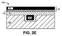
貼り合わせ基板203の部分209を分離および除去したら、図2Eに示すような素子基板205を用いて、本発明の実施形態によるマルチゲートHEMT100を形成する。一実施形態では、素子基板205は、キャリア基板102と、犠牲層206と、貼り合わせ接着層104と、チャネル層120と、を有する。一実施形態では、チャネル層120は、極性半導体層114と分極層112とで構成されるヘテロ構造である。いくつかの実施形態において、極性半導体層114は、分極層112の上に直接配置される。 After the
次に、図2Fに示すように、キャリア基板102の上で犠牲層206の相対する両側に、ソースコンタクト110およびドレインコンタクト110を形成する。ソースコンタクト110およびドレインコンタクト110は、極性半導体層114からのエピタキシャル成長によって形成することができる。例えば、ソースコンタクト110およびドレインコンタクト110は、ALDまたはCVDによって形成することができる。一実施形態では、ソースコンタクト110およびドレインコンタクト110は、極性半導体層114を貫通して延在して、分極層112の上に直接形成される。これにより、ソースコンタクト110およびドレインコンタクト110は、極性半導体層114および分極層112に結合される。さらに、ソースコンタクト110およびドレインコンタクト110は、極性半導体層114内に形成された2DEG層に結合され得る。ソースコンタクト110およびドレインコンタクト110は、任意の適切な半導体材料で形成される。一実施形態では、ソースコンタクト110およびドレインコンタクト110は、nドープGaN、InGaN、またはInNで形成される。 Next, as illustrated in FIG. 2F, the
その後、図2G−1に示すように、犠牲層206を選択的に除去することで、ボイド210を形成する。一実施形態では、犠牲層206は、犠牲層206のみを主に除去する第1のエッチングプロセスによって除去される。一実施形態では、第1のエッチングプロセスは、周囲の貼り合わせ接着層104に対して選択的に犠牲層206を除去するエッチャントを用いた等方性ウェットエッチングプロセスである。すなわち、そのエッチャントは、周囲の貼り合わせ接着層104は略無傷のまま残して、犠牲層206を主に除去する。一実施形態では、エッチャントは、リン酸(H3PO4)、または水酸化アンモニウムと過酸化水素の混合物(NH4OH+H2O2)である。Thereafter, as shown in FIG. 2G-1, the
犠牲層206を除去するために、図2G−2の透視上面図に示すように、犠牲層206の真上の領域部分209を貫通する少なくとも1つまたはいくつかの開口部211を形成することができる。これらの開口部211は、チャネル層120と干渉しない。一実施形態では、開口部211は、犠牲層206を露出させるとともに、エッチャントが通って流れ得るトンネルを提供する。エッチャントは、犠牲層206を選択的に除去するために使用することができる。いくつかの実施形態において、開口部211は、プラズマエッチングプロセスなどの任意の適切なエッチングプロセスによって形成してよい。 In order to remove the
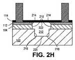
次に、図2Hに示すように、ボイド210を拡張することで、拡張ボイド212を形成する。一実施形態では、分極層112の一部を除去することで、拡張ボイド212を形成する。これにより、拡張ボイド212で、極性半導体層114の下面222を露出させることができる。拡張ボイド212によって、さらに、素子基板205内のその他の面も露出させることができる。例えば、拡張ボイド212は、分極層112の側壁214、貼り合わせ接着層104の側壁216、およびキャリア基板102の面218、220をさらに露出させることができる。拡張ボイド212は、図1A〜1Bに示す下部ゲート電極108のゲート長を規定し得る。別の実施形態では、拡張ボイド212は、図2K〜2Mでさらに後述するように、極性半導体層114を露出させない。 Next, as shown in FIG. 2H, the
いくつかの実施形態において、拡張ボイド212は、2つのエッチングプロセスによって形成される。例えば、拡張ボイド212は、第2のエッチングプロセスと第3のエッチングプロセスによって形成することができる。一実施形態では、第2のエッチングプロセスは、貼り合わせ接着層104の部分のみを主に除去する。第2のエッチングプロセスは、周囲の層(すなわち、112および102)に対して選択的に貼り合わせ接着層104を除去するエッチャントを用いた等方性ウェットエッチングプロセスであり得る。すなわち、そのエッチャントは、周囲の層は略無傷のまま残して、貼り合わせ接着層104を主に除去する。一実施形態では、エッチャントは、フッ化水素酸(HF)である。 In some embodiments, the
一実施形態では、第3のエッチングプロセスは、分極層112の部分を除去する。第3のエッチングプロセスは、周囲の層(すなわち、114、104、および102)に対して選択的に分極層112を除去するウェットエッチングプロセスであり得る。すなわち、そのエッチャントは、周囲層114、104、および102を略無傷のまま残して、分極層112を主に除去する。一実施形態では、エッチャントは、水酸化カリウム(KOH)、水酸化ナトリウム(NaOH)、またはフォトレジスト現像液AZ400Kである。 In one embodiment, the third etching process removes portions of the
次に、図2Iに示すように、第1のゲート誘電体層116および第2のゲート誘電体層118を形成する。いくつかの実施形態において、第1のゲート誘電体層116は、チャネル層120の上でソースコンタクト110とドレインコンタクト110との間に形成される。また、第2のゲート誘電体層118は、拡張ボイド212の面222、214、216、218、220上に形成される。いくつかの実施形態において、第2のゲート誘電体層118は、拡張ボイド212を完全には充填しない。第1と第2のゲート誘電体層116、118は、トランジスタの動作のための十分な厚さを有するように形成される。一実施形態では、第1と第2のゲート誘電体層116、118は、2〜4nmの厚さを有する。第1と第2のゲート誘電体層116、118は、それらが形成された面を、後に形成されるゲート電極から電気的に絶縁する。第1と第2のゲート誘電体層116、118は、任意の適切なHigh−k誘電体材料で形成してよい。一実施形態では、第1と第2のゲート誘電体層116、118は、SiO2、HfO2、およびZrO2などの絶縁材料で形成されるが、ただし、これらに限定されない。Next, as shown in FIG. 2I, a first
いくつかの実施形態において、CVDまたはALDなどの任意の適切なコンフォーマル堆積プロセスによって、第1と第2のゲート誘電体層116、118を形成することができる。一実施形態では、第1と第2のゲート誘電体層116、118を同時に形成する。一実施形態では、第2のゲート誘電体層118は、図2G−2で上述した開口部211を介したALDによって形成される。この場合、開口部211は、第2のゲート誘電体層118を堆積させるための十分な堆積材料を、拡張ボイド212内に流入させるのに十分に広い直径を有するように設計されなければならない。一実施形態では、開口部211は、少なくとも10nmの直径を有する。具体的な実施形態では、開口部211は、15〜20nmの範囲の直径を有する。 In some embodiments, the first and second gate dielectric layers 116, 118 can be formed by any suitable conformal deposition process, such as CVD or ALD. In one embodiment, the first and second gate dielectric layers 116, 118 are formed simultaneously. In one embodiment, the second
その後、図2Jに示すように、第1のゲート電極106および第2のゲート電極108を形成することで、本発明の実施形態によるエンハンスメント型マルチゲートHEMT100の構成を完成させる。第1のゲート電極106は、極性半導体層114の上方で第1のゲート誘電体層116の上に形成される。さらに、第2のゲート電極108は、極性半導体層114の下方で拡張ボイド212内に形成される。一実施形態では、第2のゲート電極108は、拡張ボイド212を完全に充填する。一実施形態では、第2のゲート電極108は、第2のゲート誘電体層118の範囲内で完全に包囲される。第1のゲート電極106および第2のゲート電極108は、設計要件に応じたゲート長を有するように形成することができる。いくつかの実施形態において、第1と第2のゲート電極は、極性半導体層114の深さDに応じたゲート長を有し得る。例えば、極性半導体層114の深さDが約20nmである場合には、第1と第2のゲート電極106、108は、同じゲート長を有し得る。一実施形態では、第1と第2のゲート電極106、108は、1〜3μmのゲート長を有し得る。具体的な実施形態では、第1と第2のゲート電極106、108は、2μmのゲート長を有する。他の例では、極性半導体層114の深さDが約100nmである場合に、第1と第2のゲート電極106、108は、異なるゲート長を有し得る。例えば、第2のゲート電極108は、第1のゲート電極106よりも大きいゲート長を有し得る。一実施形態では、第1のゲート電極106は、0.5〜3μmのゲート長を有してよく、第2のゲート電極は、1〜3μmのゲート長を有してよい。具体的な実施形態では、第1のゲート電極106は1μmのゲート長を有し、第2のゲート電極108は2μmのゲート長を有する。 Thereafter, as shown in FIG. 2J, the
一実施形態では、第1のゲート電極106と第2のゲート電極108は、互いに垂直方向に位置合わせされる。さらに、一実施形態では、第1のゲート電極106と第2のゲート電極108は、一方のゲートに電圧が印加されたときに他方のゲートにも同じ電圧が印加されるように、互いに電気的に結合される。これにより、極性半導体層114を通り抜ける電流の流れを、チャネル層120の両側を用いて制御することが可能である。第1のゲート電極106は、任意の適切なゲート形成プロセスによって形成してよい。例えば、第1のゲート電極106は、導電性材料のブランケット堆積と、続いて、その堆積された導電性材料の異方性エッチングによって形成することができる。他の例では、第1の電極106は、置換ゲートプロセスまたはダマシンプロセスによって形成することができる。第2のゲート電極108は、基板内に埋め込まれたボイドの範囲内に材料を堆積させることが可能な任意の適切な堆積手法によって形成してよい。例えば、第2のゲート電極108は、CVD、PVD、またはALDによって形成することができる。具体的な実施形態では、第1と第2のゲート電極106、108を同時に形成する。第1と第2のゲート電極106、108は、CVD、PVD、またはALDと、続いて、第1のゲート電極106を形成するための異方性エッチングによって形成することができる。第1と第2のゲート電極106、108は、金属などの導電性材料で形成することができる。典型例となる金属として、Ni、TiN、Pt、およびWが含まれる。 In one embodiment, the
本発明の一実施形態によれば、図2Jに示すエンハンスメント型マルチゲートHEMT100は、第1のゲート電極106と第2のゲート電極108との間に配置された極性半導体層114を有する。本実施形態では、分極層112は、第1のゲート電極106と第2のゲート電極108との間には配置されていない。第1のゲート電極106と第2のゲート電極108との間に分極層112が存在しないことで、第1のゲート電極106と第2のゲート電極108との間では2DEGの形成が抑止される。本発明の実施形態によれば、第1のゲート電極106と第2のゲート電極108にゲートバイアスを印加することによって、極性半導体層114の上方と下方からチャネル層120を制御する。これにより、本発明の一実施形態によるエンハンスメント型マルチゲートHEMT100は、極性半導体層114を通り抜ける電流の流れを最大限に制御できる。 According to one embodiment of the present invention, the enhancement
別の実施形態では、デプリーション型マルチゲートHEMTを形成するために、第1のゲート電極106と第2のゲート電極108との間の分極層112を無傷のまま残すことができる。デプリーション型マルチゲートHEMTを形成する方法を、上記の図2G−1から続く図2K〜2Mに示している。 In another embodiment, the
図2Kでは、図2G−1のボイド210を拡張することで、拡張ボイド212を形成する。本実施形態では、拡張ボイド212は、極性半導体層114を露出させない。拡張ボイド212によって、分極層112の下面223を露出させることができる。いくつかの実施形態において、拡張ボイド212は、さらに、貼り合わせ接着層104の側壁216、およびキャリア基板102の面218、220を露出させることができる。拡張ボイド212は、図2Hに関して上述したように、貼り合わせ接着層104のみを主に除去する第2のエッチングプロセスによって形成することができる。次に、図2Lに示すように、第1のゲート誘電体層116および第2のゲート誘電体層118を形成する。本実施形態では、第1のゲート誘電体層116は、チャネル層120の上でソースコンタクト110とドレインコンタクト110との間に形成される。また、第2のゲート誘電体層118は、拡張ボイド212の面223、216、218、220上に形成される。第2のゲート誘電体層118は、拡張ボイド212を完全には充填しない。一実施形態では、第2のゲート誘電体118の一部は、分極層112の真下に形成される。第1のゲート誘電体層116および第2のゲート誘電体層118は、図2Iで上述したものと同様の厚さ、寸法を有し、同様のプロセス技術で形成される。 In FIG. 2K, the expanded
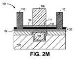
その後、図2Mに示すように、第1のゲート電極106および第2のゲート電極108を形成することで、本発明の実施形態によるデプリーション型マルチゲートHEMT101の構成を完成させる。いくつかの実施形態において、第1のゲート電極106は、チャネル層120の上方で第1のゲート誘電体層116の上に形成される。第2のゲート電極108は、拡張ボイド212内に形成される。第2のゲート電極108は、極性半導体層114と分極層112とで構成されたチャネル層120の下方に配置することができる。一実施形態では、第2のゲート電極108は、第2のゲート誘電体層118によって完全に包囲される。一実施形態では、第1のゲート電極106と第2のゲート電極108は、互いに垂直方向に位置合わせされる。さらに、一実施形態では、第1のゲート電極106と第2のゲート電極108は、一方のゲートに電圧が印加されたときに他方のゲートにも同じ電圧が印加されるように、互いに電気的に結合される。これにより、チャネル層120を通り抜ける電流の流れを、チャネル層120の両側を用いて制御することが可能である。一実施形態では、第1のゲート電極106および第2のゲート電極108は、上記の図2Jで開示したプロセス技術および構造寸法によって形成される。 Thereafter, as shown in FIG. 2M, the
本発明の一実施形態によれば、デプリーション型マルチゲートHEMT101は、第1のゲート電極106と第2のゲート電極108との間に、極性半導体層114と分極層112の両方が配置される。これによって、デプリーション型マルチゲートHEMT101は、第1のゲート電極106と第2のゲート電極108との間に2DEGを有する。一実施形態では、2DEGは、極性半導体層114内で界面から1〜2nmの距離にある。本発明の実施形態によれば、第1のゲート電極106と第2のゲート電極108にゲートバイアスを印加することによって、極性半導体層114の上方と下方からチャネル層120を制御する。これにより、本発明の一実施形態によるデプリーション型マルチゲートHEMT101は、チャネル層120を通り抜ける電流の流れを最大限に制御できる。 According to one embodiment of the present invention, the depletion
図3は、本発明の実施形態により製造された1つ以上のダイを含むインタポーザ300を示している。インタポーザ300は、第1の基板302を第2の基板304にブリッジするために使用される介在基板である。第1の基板302は、例えば、集積回路ダイであってよい。第2の基板304は、例えば、メモリモジュール、コンピュータマザーボード、または他の集積回路ダイであってよい。一般的に、インタポーザ300の目的は、配線接続をより広いピッチ幅に広げること、または配線接続を別の接続へと再ルーティングすることである。例えば、インタポーザ300は、集積回路ダイをボールグリッドアレイ(BGA)306に結合することができ、そしてこれが次に第2の基板304に結合されることが可能である。一部の実施形態では、第1と第2の基板302/304は、インタポーザ300の相対する側に装着される。他の実施形態では、第1と第2の基板302/304は、インタポーザ300の同じ側に装着される。さらなる実施形態では、インタポーザ300によって3つ以上の基板が相互接続される。 FIG. 3 illustrates an
インタポーザ300は、エポキシ樹脂、ガラス繊維強化エポキシ樹脂、セラミック材料、またはポリイミドなどのポリマ材料で形成することができる。さらなる実施形態では、インタポーザは、代替の剛性材料または可撓性材料で形成することができ、それらの材料として、シリコン、ゲルマニウム、他のIII−V族およびIV族の材料など、半導体基板で使用するための上述のものと同じ材料を含むことができる。 The
インタポーザは、金属配線308およびビア310を有してよく、それらのビアとして、限定するものではないが、シリコン貫通ビア(TSV)312が含まれる。インタポーザ300は、さらに埋め込み素子314を有してよく、それらには、受動素子と能動素子の両方が含まれる。そのような素子として、キャパシタ、デカップリングキャパシタ、抵抗、インダクタ、ヒューズ、ダイオード、変圧器、センサ、および静電放電(ESD)素子が含まれるが、ただし、これらに限定されない。さらに、高周波(RF)素子、電力増幅器、パワーマネジメント素子、アンテナ、アレイ、センサ、およびMEMS素子のような、より複雑な素子をインタポーザ300上に形成してもよい。 The interposer may have
本発明の実施形態によれば、本明細書で開示するマルチゲートHEMT、またはマルチゲートHEMTを形成する方法を、インタポーザ基板300の製造において用いることができる。 According to embodiments of the present invention, the multi-gate HEMT disclosed herein or a method of forming a multi-gate HEMT can be used in the manufacture of the
図4は、本発明の一実施形態によるコンピュータ装置400を示している。コンピュータ装置400は、いくつかのコンポーネントを含み得る。一実施形態では、それらのコンポーネントは、1つ以上のマザーボードに装着される。別の実施形態では、それらのコンポーネントは、マザーボードではなく単一のシステムオンチップ(SoC)ダイ上に作製される。コンピュータ装置400内のコンポーネントとして、集積回路ダイ402および少なくとも1つの通信チップ408が含まれるが、ただし、これらに限定されない。一部の実装形態では、通信チップ408は、集積回路ダイ402の一部として作製される。集積回路ダイ402は、CPU404ならびにオンダイメモリ406を有してよく、オンダイメモリは、キャッシュメモリとしてよく使用されるものであって、混載DRAM(eDRAM)またはスピントランスファトルクメモリ(STTMまたはSTTM−RAM)などの技術によって提供することが可能である。 FIG. 4 shows a
コンピュータ装置400は、他のコンポーネントを含んでよく、それらは、マザーボードに物理的および電気的に結合されたものであっても、結合されていないものであってもよく、またはSoCダイ内に作製されたものであってよい。このような他のコンポーネントとして、揮発性メモリ410(例えば、DRAM)、不揮発性メモリ412(例えば、ROMまたはフラッシュメモリ)、グラフィック処理装置414(GPU)、デジタル信号プロセッサ416、暗号プロセッサ442(ハードウェア内で暗号アルゴリズムを実行する専用プロセッサ)、チップセット420、アンテナ422、ディスプレイまたはタッチスクリーンディスプレイ424、タッチスクリーンコントローラ426、バッテリ428または他の電源、電力増幅器(図示せず)、グローバルポジショニングシステム(GPS)装置428、コンパス430、モーション・コプロセッサまたはセンサ432(加速度計、ジャイロスコープ、コンパスを含み得る)、スピーカ434、カメラ436、ユーザ入力装置438(キーボード、マウス、スタイラス、タッチパッドなど)、およびマスストレージデバイス440(ハードディスクドライブ、コンパクトディスク(CD)、デジタル多用途ディスク(DVD)など)が含まれるが、ただし、これらに限定されない。 The
通信チップ408は、コンピュータ装置400に出入りするデータ伝送のための無線通信を可能とする。「無線」という用語およびその派生語は、非固形媒体を介した変調電磁放射を用いることによりデータを通信し得る回路、デバイス、システム、方法、技術、通信チャネルなどを記述するために使用されることがある。この用語は、関連したデバイスがワイヤを含まないことを意味するものではないが、一部の実施形態では、ワイヤを含まないことがある。通信チップ408は、いくつかの無線規格またはプロトコルのいずれかを実行することができ、それらの無線規格またはプロトコルとして、Wi−Fi(IEEE802.11ファミリ)、WiMAX(IEEE802.16ファミリ)、IEEE802.20、ロングタームエボリューション(LTE)、Ev−DO、HSPA+、HSDPA+、HSUPA+、EDGE、GSM(登録商標)、GPRS、CDMA、TDMA、DECT、Bluetooth(登録商標)、これらの派生型、ならびに3G、4G、5G、およびそれ以降のものとして表される他のいずれかの無線プロトコルが含まれるが、ただし、これらに限定されない。コンピュータ装置400は、複数の通信チップ408を含み得る。例えば、第1の通信チップ408は、Wi−FiおよびBluetooth(登録商標)のような短距離無線通信に専用のものであってよく、第2の通信チップ408は、GPS、EDGE、GPRS、CDMA、WiMAX、LTE、Ev−DOなどのような遠距離無線通信に専用のものであってよい。 The
コンピュータ装置400のプロセッサ404は、本発明の実施形態により形成され得る本発明の実施形態のマルチゲートHEMTデバイスを1つ以上含み得る。「プロセッサ」という用語は、レジスタおよび/またはメモリからの電子データを処理して、その電子データを、レジスタおよび/またはメモリに記憶されることがある他の電子データに変換する任意のデバイスまたはデバイスの部分を指し得る。 The
また、通信チップ408も、本発明の実施形態により形成され得る本発明の実施形態のマルチゲートHEMTデバイスを1つ以上含み得る。
さらなる実施形態では、コンピュータ装置400内に収容された他のコンポーネントは、本発明の実施形態により形成され得る本発明の実施形態のマルチゲートHEMTデバイスを1つ以上含み得る。 In further embodiments, other components housed within the
種々の実施形態において、コンピュータ装置400は、ラップトップコンピュータ、ネットブックコンピュータ、ノートブックコンピュータ、ウルトラブックコンピュータ、スマートフォン、タブレット、パーソナルデジタルアシスタント(PDA)、ウルトラモバイルPC、携帯電話機、デスクトップコンピュータ、サーバ、プリンタ、スキャナ、モニタ、セットトップボックス、エンタテイメントコントロールユニット、デジタルカメラ、携帯音楽プレーヤ、またはデジタルビデオレコーダであってよい。さらなる実施形態では、コンピュータ装置400は、データを処理する他の任意の電子機器であってよい。 In various embodiments, the
一実施形態では、半導体デバイスは、基板と、基板の上の接着層と、接着層の上のチャネル層と、チャネル層の上の第1のゲート電極であって、この第1のゲート電極とチャネル層との間に第1のゲート誘電体層を有する第1のゲート電極と、チャネル層の下の第2のゲート電極であって、この第2のゲート電極を完全に取り囲む第2のゲート誘電体層を有する第2のゲート電極と、第1のゲート電極の相対する両側に配置された一対のソースコンタクトおよびドレインコンタクトと、を含む。 In one embodiment, a semiconductor device includes a substrate, an adhesive layer on the substrate, a channel layer on the adhesive layer, and a first gate electrode on the channel layer, the first gate electrode A first gate electrode having a first gate dielectric layer between the channel layer and a second gate electrode under the channel layer, the second gate completely surrounding the second gate electrode A second gate electrode having a dielectric layer; and a pair of source and drain contacts disposed on opposite sides of the first gate electrode.
一実施形態では、チャネル層は、ヘテロ構造である。チャネル層は、分極層と、分極層の上に直接配置された極性半導体層と、を有し得る。分極層は、AlGaNで形成することができ、極性半導体層は、GaNで形成することができる。一実施形態では、分極層は、第1のゲート電極と第2のゲート電極との間には配置されていない。一実施形態では、極性半導体層および分極層は、第1のゲート電極と第2のゲート電極との間に配置されている。一実施形態では、分極層は、分極層と極性半導体層との間の界面において2次元電子ガス(2DEG)を誘起する。2DEGは、極性半導体層内で界面から1〜2nmの距離にあり得る。一実施形態では、一対のソースコンタクトおよびドレインコンタクトは、極性半導体層を貫通して、分極層上に形成される。一実施形態では、第1のゲート誘電体層は、一対のソースコンタクトおよびドレインコンタクト間に形成される。第2のゲート電極は、キャリア基板のトレンチ内へと延出したものであってよい。一実施形態では、第1のゲート電極は、第2のゲート電極に対して垂直方向に位置合わせされている。 In one embodiment, the channel layer is a heterostructure. The channel layer can have a polarization layer and a polar semiconductor layer disposed directly on the polarization layer. The polarization layer can be formed of AlGaN, and the polar semiconductor layer can be formed of GaN. In one embodiment, the polarization layer is not disposed between the first gate electrode and the second gate electrode. In one embodiment, the polar semiconductor layer and the polarization layer are disposed between the first gate electrode and the second gate electrode. In one embodiment, the polarization layer induces a two-dimensional electron gas (2DEG) at the interface between the polarization layer and the polar semiconductor layer. 2DEG can be at a distance of 1-2 nm from the interface in the polar semiconductor layer. In one embodiment, a pair of source and drain contacts are formed on the polarization layer, penetrating the polar semiconductor layer. In one embodiment, the first gate dielectric layer is formed between a pair of source and drain contacts. The second gate electrode may extend into the trench in the carrier substrate. In one embodiment, the first gate electrode is aligned perpendicular to the second gate electrode.
一実施形態では、半導体デバイスを形成する方法は、ドナー基板と、埋め込み犠牲層を有する受容側基板と、を準備することと、その最上部がチャネル層を構成する素子基板を形成するためにドナー基板の一部を受容側基板に転写することと、埋め込み犠牲層の相対する両側でチャネル層上に一対のソース領域およびドレイン領域を形成することと、チャネル層の下方にボイドを形成するために埋め込み犠牲層を除去することと、チャネル層の一部の上に第1のゲート誘電体層と、ボイド内の側壁上に第2のゲート誘電体層と、を形成することと、チャネル層の上方で第1のゲート誘電体層上に第1のゲート電極と、チャネル層の下方でボイド内の第2のゲート誘電体層上に第2のゲート電極と、を形成することと、を含む。 In one embodiment, a method of forming a semiconductor device includes providing a donor substrate and a receiving substrate having a buried sacrificial layer, and forming a donor substrate to form an element substrate, the top of which forms a channel layer. To transfer a portion of the substrate to the receiving substrate, to form a pair of source and drain regions on the channel layer on opposite sides of the buried sacrificial layer, and to form a void below the channel layer Removing the buried sacrificial layer; forming a first gate dielectric layer on a portion of the channel layer; and a second gate dielectric layer on a sidewall in the void; and Forming a first gate electrode on the first gate dielectric layer above and a second gate electrode on the second gate dielectric layer in the void below the channel layer. .
一実施形態では、ボイドを形成することは、第1と第2の選択的エッチングプロセスを含む。第1の選択的エッチングプロセスは、犠牲層のみを主に除去し得る。第2の選択的エッチングプロセスは、接着層のみを主に除去し得る。一実施形態では、第2の選択的エッチングプロセスは、第3の選択的エッチングプロセスをさらに含む。第3の選択的エッチングプロセスは、ボトム層の一部を主に除去し得る。一実施形態では、ボイドを形成することによって、ゲート用ボイド内でボトム層を露出させる。ボイドを形成することによって、ボイド内でトップ層を露出させることができる。一実施形態では、犠牲層を選択的に除去することは、犠牲層を露出させるための開口部を素子基板にエッチングすることと、開口部を通して施される選択的エッチャントによって犠牲層を除去することと、を含む。選択的エッチャントは、周囲の材料に対して選択的に犠牲層を除去し得る。一実施形態では、ドナー基板の一部を受容側基板に転写することは、ドナー基板を受容側基板に装着することと、貼り合わせ基板を形成するためにドナー基板を受容側基板に貼り合わせることと、素子基板を形成するために貼り合わせ基板を分離することと、を含む。素子基板は、受容側基板と、受容側基板の上にあるドナー基板の一部と、を含み得る。一実施形態では、ドナー基板の一部を受容側基板に転写することは、ドナー基板を受容側基板に接着させるために融着を実施することをさらに含む。 In one embodiment, forming the void includes first and second selective etching processes. The first selective etching process can mainly remove only the sacrificial layer. The second selective etching process can mainly remove only the adhesive layer. In one embodiment, the second selective etching process further includes a third selective etching process. The third selective etching process can mainly remove a portion of the bottom layer. In one embodiment, the bottom layer is exposed within the gate void by forming a void. By forming the void, the top layer can be exposed in the void. In one embodiment, selectively removing the sacrificial layer includes etching an opening in the device substrate to expose the sacrificial layer and removing the sacrificial layer with a selective etchant applied through the opening. And including. The selective etchant can selectively remove the sacrificial layer relative to the surrounding material. In one embodiment, transferring a portion of the donor substrate to the receiving substrate includes attaching the donor substrate to the receiving substrate and bonding the donor substrate to the receiving substrate to form a bonded substrate. And separating the bonded substrate to form an element substrate. The device substrate can include a receiving substrate and a portion of a donor substrate overlying the receiving substrate. In one embodiment, transferring a portion of the donor substrate to the receiving substrate further includes performing a fusion to adhere the donor substrate to the receiving substrate.
一実施形態では、コンピュータ装置は、マザーボードと、マザーボードに実装されたプロセッサと、プロセッサと同じチップ上に作製された通信チップ、またはマザーボードに実装された通信チップと、を備える。プロセッサは、基板と、基板の上の接着層と、接着層の上のチャネル層と、チャネル層の上の第1のゲート電極であって、この第1のゲート電極とチャネル層との間に第1のゲート誘電体層を有する第1のゲート電極と、チャネル層の下で基板内に埋め込まれた第2のゲート電極であって、この第2のゲート電極を完全に取り囲む第2のゲート誘電体層を有する第2のゲート電極と、第1のゲート電極の相対する両側に配置された一対のソースコンタクトおよびドレインコンタクトと、を含む。 In one embodiment, the computer apparatus includes a motherboard, a processor mounted on the motherboard, and a communication chip manufactured on the same chip as the processor or a communication chip mounted on the motherboard. The processor includes a substrate, an adhesive layer on the substrate, a channel layer on the adhesive layer, and a first gate electrode on the channel layer, between the first gate electrode and the channel layer. A first gate electrode having a first gate dielectric layer and a second gate electrode embedded in the substrate under the channel layer, the second gate electrode completely surrounding the second gate electrode A second gate electrode having a dielectric layer; and a pair of source and drain contacts disposed on opposite sides of the first gate electrode.
一実施形態では、チャネル層は、ヘテロ構造である。一実施形態では、チャネル層は、分極層と、分極層の上に直接配置された極性半導体層と、を有する。分極層は、分極層と極性半導体層との間の界面において2次元電子ガス(2DEG)を誘起し得る。分極層は、AlGaNで形成することができ、極性半導体層は、GaNで形成することができる。一実施形態では、第1のゲート電極は、第2のゲート電極に対して垂直方向に位置合わせされている。 In one embodiment, the channel layer is a heterostructure. In one embodiment, the channel layer has a polarization layer and a polar semiconductor layer disposed directly on the polarization layer. The polarization layer can induce a two-dimensional electron gas (2DEG) at the interface between the polarization layer and the polar semiconductor layer. The polarization layer can be formed of AlGaN, and the polar semiconductor layer can be formed of GaN. In one embodiment, the first gate electrode is aligned perpendicular to the second gate electrode.
本発明の図示の実施形態についての上記説明は、要約に記載されているものも含めて、網羅的なものではなく、開示した厳密な形態に本発明を限定するものでもない。本明細書では、例示目的で、本発明の具体的な実施形態、および本発明のための具体例について記載しているものの、当業者であれば理解できるように、本発明の範囲内で種々の均等な変更が可能である。 The above description of illustrated embodiments of the invention, including those described in the summary, is not exhaustive and is not intended to limit the invention to the precise forms disclosed. While specific embodiments of the present invention and specific examples for the present invention have been described herein for purposes of illustration, various modifications within the scope of the present invention will be appreciated by those skilled in the art. Can be changed evenly.
かかる変更は、上記の詳細な説明に照らして、本発明に対して実施することができる。以下の請求項において使用される用語は、本明細書および請求項に開示の特定の実施形態に発明を限定するものと解釈されてはならない。むしろ、本発明の範囲は、確立されたクレーム解釈論に従って解釈されるべき以下の請求項によって、完全に決定されるべきである。 Such modifications can be made to the invention in light of the above detailed description. The terms used in the following claims should not be construed to limit the invention to the specific embodiments disclosed in the specification and the claims. Rather, the scope of the present invention should be determined entirely by the following claims, which are to be construed in accordance with established claim interpretation.
Claims (26)
Translated fromJapanese基板と、
前記基板の上の接着層と、
前記接着層の上のチャネル層と、
前記チャネル層の上の第1のゲート電極であって、該第1のゲート電極と前記チャネル層との間に第1のゲート誘電体層を有する第1のゲート電極と、
前記チャネル層の下の第2のゲート電極であって、該第2のゲート電極を完全に取り囲み、前記接着層の側壁、前記基板の上面、および前記チャネル層の面上に形成される第2のゲート誘電体層を有する第2のゲート電極と、
前記第1のゲート電極の相対する両側に配置された一対のソースコンタクトおよびドレインコンタクトと、を含む半導体デバイス。A semiconductor device,
A substrate,
An adhesive layer on the substrate;
A channel layer on the adhesive layer;
A first gate electrode on the channel layer, the first gate electrode having a first gate dielectric layer between the first gate electrode and the channel layer;
A second gate electrode under said channel layer,enclose takes completely the gate electrodes of thesecond, is formed on the sidewall of the adhesive layer, the upper surface of the substrate, and on the surface of the channel layer A second gate electrode having a second gate dielectric layer;
A semiconductor device comprising a pair of source and drain contacts disposed on opposite sides of the first gate electrode.
基板と、 A substrate,
前記基板の上の接着層と、 An adhesive layer on the substrate;
前記接着層の上のチャネル層と、 A channel layer on the adhesive layer;
前記チャネル層の上の第1のゲート電極であって、該第1のゲート電極と前記チャネル層との間に第1のゲート誘電体層を有する第1のゲート電極と、 A first gate electrode on the channel layer, the first gate electrode having a first gate dielectric layer between the first gate electrode and the channel layer;
前記チャネル層の下の第2のゲート電極であって、該第2のゲート電極を完全に取り囲む第2のゲート誘電体層を有する第2のゲート電極と、 A second gate electrode below the channel layer, the second gate electrode having a second gate dielectric layer that completely surrounds the second gate electrode;
前記第1のゲート電極の相対する両側に配置された一対のソースコンタクトおよびドレインコンタクトと、を含み、 A pair of source and drain contacts disposed on opposite sides of the first gate electrode,
前記第2のゲート電極は、前記基板のトレンチ内へと延出している、半導体デバイス。 The semiconductor device, wherein the second gate electrode extends into a trench in the substrate.
ドナー基板と、埋め込まれた状態の犠牲層を有する受容側基板と、を準備することと、
その最上部がチャネル層を構成する素子基板を形成するために、前記ドナー基板の一部を前記受容側基板に転写することと、
前記埋め込まれた状態の犠牲層の相対する両側における前記チャネル層上に、一対のソース領域およびドレイン領域を形成することと、
前記チャネル層の下方にボイドを形成するために、前記埋め込まれた状態の犠牲層を除去することと、
前記チャネル層の一部の上に第1のゲート誘電体層と、前記ボイド内の側壁上に第2のゲート誘電体層と、を形成することと、
前記チャネル層の上方で前記第1のゲート誘電体層上に第1のゲート電極と、前記チャネル層の下方で前記ボイド内の前記第2のゲート誘電体層上に第2のゲート電極と、を形成することと、を含む方法。A method of forming a semiconductor device comprising:
Providing a donor substrate and a receiving substrate having an embedded sacrificial layer;
Transferring a portion of the donor substrate to the receiving substrate to form an element substrate, the top of which forms a channel layer;
Forming a pair of source and drain regions on the channel layer on opposite sides of the buried sacrificial layer;
Removing the buried sacrificial layer to form a void below the channel layer;
Forming a first gate dielectric layer on a portion of the channel layer and a second gate dielectric layer on a sidewall in the void;
A first gate electrode on the first gate dielectric layer above the channel layer; a second gate electrode on the second gate dielectric layer in the void below the channel layer; Forming a method.
前記ドナー基板を前記受容側基板に装着することと、
貼り合わせ基板を形成するために、前記ドナー基板を前記受容側基板に貼り合わせることと、
前記素子基板を形成するために、前記貼り合わせ基板を分離することと、を含み、
前記素子基板は、前記受容側基板と、前記受容側基板の上にある前記ドナー基板の一部と、を含む、請求項11から18のいずれか一項に記載の方法。Transferring a portion of the donor substrate to the receiving substrate;
Mounting the donor substrate to the receiving substrate;
Bonding the donor substrate to the receiving substrate to form a bonded substrate;
Separating the bonded substrate to form the element substrate,
The method according to any one of claims 11 to 18, wherein the element substrate includes the receiving substrate and a portion of the donor substrate overlying the receiving substrate.
マザーボードと、
前記マザーボードに実装されたプロセッサと、
前記プロセッサと同じチップ上に作製された通信チップ、または前記マザーボードに実装された通信チップと、を備え、
前記プロセッサは、
基板と、
前記基板の上の接着層と、
前記接着層の上のチャネル層と、
前記チャネル層の上の第1のゲート電極であって、該第1のゲート電極と前記チャネル層との間に第1のゲート誘電体層を有する第1のゲート電極と、
前記チャネル層の下で前記基板内に埋め込まれた第2のゲート電極であって、該第2のゲート電極を完全に取り囲み、前記接着層の側壁、前記基板の上面、および前記チャネル層の面上に形成される第2のゲート誘電体層を有する第2のゲート電極と、
前記第1のゲート電極の相対する両側に配置された一対のソースコンタクトおよびドレインコンタクトと、を含む、コンピュータ装置。A computer device,
With the motherboard,
A processor mounted on the motherboard;
A communication chip manufactured on the same chip as the processor, or a communication chip mounted on the motherboard,
The processor is
A substrate,
An adhesive layer on the substrate;
A channel layer on the adhesive layer;
A first gate electrode on the channel layer, the first gate electrode having a first gate dielectric layer between the first gate electrode and the channel layer;
A second gate electrode buried in said substrate under said channel layer,enclose takes completely the gate electrodes of thesecond, the sidewall of the adhesive layer, the upper surface of the substrate, and the channel layer A second gate electrode having a second gate dielectric layerformed on the surface thereof ;
And a pair of source and drain contacts arranged on opposite sides of the first gate electrode.
マザーボードと、 With the motherboard,
前記マザーボードに実装されたプロセッサと、 A processor mounted on the motherboard;
前記プロセッサと同じチップ上に作製された通信チップ、または前記マザーボードに実装された通信チップと、を備え、 A communication chip manufactured on the same chip as the processor, or a communication chip mounted on the motherboard,
前記プロセッサは、 The processor is
基板と、 A substrate,
前記基板の上の接着層と、 An adhesive layer on the substrate;
前記接着層の上のチャネル層と、 A channel layer on the adhesive layer;
前記チャネル層の上の第1のゲート電極であって、該第1のゲート電極と前記チャネル層との間に第1のゲート誘電体層を有する第1のゲート電極と、 A first gate electrode on the channel layer, the first gate electrode having a first gate dielectric layer between the first gate electrode and the channel layer;
前記チャネル層の下で前記基板内に埋め込まれた第2のゲート電極であって、該第2のゲート電極を完全に取り囲む第2のゲート誘電体層を有する第2のゲート電極と、 A second gate electrode embedded in the substrate under the channel layer, the second gate electrode having a second gate dielectric layer that completely surrounds the second gate electrode;
前記第1のゲート電極の相対する両側に配置された一対のソースコンタクトおよびドレインコンタクトと、を含み、 A pair of source and drain contacts disposed on opposite sides of the first gate electrode,
前記第2のゲート電極は、前記基板のトレンチ内へと延出している、コンピュータ装置。 The computer device, wherein the second gate electrode extends into a trench in the substrate.
Applications Claiming Priority (1)
| Application Number | Priority Date | Filing Date | Title |
|---|---|---|---|
| PCT/US2014/054823WO2016039733A1 (en) | 2014-09-09 | 2014-09-09 | Multi-gate high electron mobility transistors and methods of fabrication |
Publications (2)
| Publication Number | Publication Date |
|---|---|
| JP2017530544A JP2017530544A (en) | 2017-10-12 |
| JP6415692B2true JP6415692B2 (en) | 2018-10-31 |
Family
ID=55459359
Family Applications (1)
| Application Number | Title | Priority Date | Filing Date |
|---|---|---|---|
| JP2017505076AActiveJP6415692B2 (en) | 2014-09-09 | 2014-09-09 | Multi-gate high electron mobility transistor and manufacturing method |
Country Status (8)
| Country | Link |
|---|---|
| US (1) | US10439057B2 (en) |
| EP (1) | EP3192101A4 (en) |
| JP (1) | JP6415692B2 (en) |
| KR (1) | KR102204259B1 (en) |
| CN (1) | CN106575669B (en) |
| MY (1) | MY188298A (en) |
| TW (1) | TWI666771B (en) |
| WO (1) | WO2016039733A1 (en) |
Families Citing this family (16)
| Publication number | Priority date | Publication date | Assignee | Title |
|---|---|---|---|---|
| KR102382054B1 (en) | 2014-11-05 | 2022-04-01 | 코닝 인코포레이티드 | Bottom-up electrolytic via plating method |
| US9490430B1 (en)* | 2015-06-26 | 2016-11-08 | Taiwan Semiconductor Manufacturing Company, Ltd. | Field effect transistors and methods of forming same |
| US10979012B2 (en)* | 2016-09-30 | 2021-04-13 | Intel Corporation | Single-flipped resonator devices with 2DEG bottom electrode |
| JP6901880B2 (en)* | 2017-03-17 | 2021-07-14 | 株式会社東芝 | Nitride semiconductor device |
| TWI608607B (en)* | 2017-06-23 | 2017-12-11 | 國立臺灣師範大學 | Multi-gate high electron mobility transistor with aligned internal gate and negative capacitance ferroelectric dielectrics and manufacturing method thereof |
| US10917966B2 (en)* | 2018-01-29 | 2021-02-09 | Corning Incorporated | Articles including metallized vias |
| US11024717B2 (en) | 2018-03-22 | 2021-06-01 | Kabushiki Kaisha Toshiba | Semiconductor device and method of manufacturing semiconductor device |
| TWI791888B (en)* | 2018-09-11 | 2023-02-11 | 美商美國亞德諾半導體公司 | Enhancement mode compound semiconductor field-effect transistor, semiconductor device, and method of manufacturing enhancement mode semiconductor device |
| CN111370306B (en)* | 2018-12-26 | 2023-04-28 | 中芯集成电路(宁波)有限公司上海分公司 | Fabrication method of transistor and structure of fully surrounded gate device |
| KR102605621B1 (en) | 2019-01-25 | 2023-11-23 | 삼성전자주식회사 | Method for manufacturing semiconductor device having buried gate electrodes |
| KR102133367B1 (en) | 2019-02-19 | 2020-07-13 | 국방과학연구소 | High electron mobility transistor and method of manufacturing the same |
| US11855198B2 (en) | 2020-04-09 | 2023-12-26 | Qualcomm Incorporated | Multi-gate high electron mobility transistors (HEMTs) employing tuned recess depth gates for improved device linearity |
| KR20210134151A (en) | 2020-04-29 | 2021-11-09 | 삼성전자주식회사 | Semiconductor device |
| DE102020128628A1 (en)* | 2020-05-28 | 2021-12-02 | Taiwan Semiconductor Manufacturing Co. Ltd. | SEMICONDUCTOR COMPONENT WITH TWO-DIMENSIONAL MATERIALS |
| WO2023058147A1 (en)* | 2021-10-06 | 2023-04-13 | 日本電信電話株式会社 | Semiconductor device |
| CN118472026B (en)* | 2024-07-11 | 2024-10-08 | 辽宁材料实验室 | Extremely-low-temperature high-electron-mobility transistor, preparation method and radio frequency amplifier |
Family Cites Families (19)
| Publication number | Priority date | Publication date | Assignee | Title |
|---|---|---|---|---|
| JP4332925B2 (en)* | 1999-02-25 | 2009-09-16 | ソニー株式会社 | Semiconductor device and manufacturing method thereof |
| EP1283422A1 (en)* | 2001-08-07 | 2003-02-12 | Lucent Technologies Inc. | Testbench for the validation of a device under test |
| KR100451459B1 (en) | 2003-02-10 | 2004-10-07 | 삼성전자주식회사 | Method for forming double gate electrode and method for forming a semiconductor device having the same |
| US6949761B2 (en)* | 2003-10-14 | 2005-09-27 | International Business Machines Corporation | Structure for and method of fabricating a high-mobility field-effect transistor |
| US7018901B1 (en) | 2004-09-29 | 2006-03-28 | Freescale Semiconductor, Inc. | Method for forming a semiconductor device having a strained channel and a heterojunction source/drain |
| JP4650224B2 (en)* | 2004-11-19 | 2011-03-16 | 日亜化学工業株式会社 | Field effect transistor |
| JP2008252086A (en) | 2007-03-12 | 2008-10-16 | Interuniv Micro Electronica Centrum Vzw | Tunnel field effect transistor with gate tunnel barrier |
| JP4854563B2 (en) | 2007-03-30 | 2012-01-18 | キヤノン株式会社 | Image reading apparatus and image forming apparatus |
| KR101498968B1 (en)* | 2007-07-05 | 2015-03-12 | 삼성전자주식회사 | Method and apparatus for resource determination for peer-to-peer communication in a communication system |
| JP2009135448A (en)* | 2007-11-01 | 2009-06-18 | Semiconductor Energy Lab Co Ltd | Method for manufacturing semiconductor substrate and method for manufacturing semiconductor device |
| US8362604B2 (en) | 2008-12-04 | 2013-01-29 | Ecole Polytechnique Federale De Lausanne (Epfl) | Ferroelectric tunnel FET switch and memory |
| JP5043899B2 (en)* | 2009-07-27 | 2012-10-10 | 日立オートモティブシステムズ株式会社 | EGR flow control device for internal combustion engine |
| US8440998B2 (en)* | 2009-12-21 | 2013-05-14 | Intel Corporation | Increasing carrier injection velocity for integrated circuit devices |
| US8030145B2 (en)* | 2010-01-08 | 2011-10-04 | International Business Machines Corporation | Back-gated fully depleted SOI transistor |
| US8901537B2 (en) | 2010-12-21 | 2014-12-02 | Intel Corporation | Transistors with high concentration of boron doped germanium |
| US9046761B2 (en)* | 2010-12-23 | 2015-06-02 | Intel Corporation | Lithography mask having sub-resolution phased assist features |
| JP5490061B2 (en)* | 2011-07-12 | 2014-05-14 | シャープ株式会社 | Registration method for image forming apparatus and image forming apparatus |
| KR20130053193A (en)* | 2011-11-15 | 2013-05-23 | 엘지전자 주식회사 | Nitride-based heterojunction semiconductor device and method for the same |
| US8669591B2 (en)* | 2011-12-27 | 2014-03-11 | Eta Semiconductor Inc. | E-mode HFET device |
- 2014
- 2014-09-09WOPCT/US2014/054823patent/WO2016039733A1/enactiveApplication Filing
- 2014-09-09KRKR1020177003140Apatent/KR102204259B1/enactiveActive
- 2014-09-09MYMYPI2017700394Apatent/MY188298A/enunknown
- 2014-09-09EPEP14901471.4Apatent/EP3192101A4/ennot_activeWithdrawn
- 2014-09-09USUS15/329,216patent/US10439057B2/ennot_activeExpired - Fee Related
- 2014-09-09JPJP2017505076Apatent/JP6415692B2/enactiveActive
- 2014-09-09CNCN201480081066.6Apatent/CN106575669B/enactiveActive
- 2015
- 2015-08-04TWTW104125225Apatent/TWI666771B/enactive
Also Published As
| Publication number | Publication date |
|---|---|
| US10439057B2 (en) | 2019-10-08 |
| US20170229565A1 (en) | 2017-08-10 |
| EP3192101A1 (en) | 2017-07-19 |
| MY188298A (en) | 2021-11-25 |
| CN106575669A (en) | 2017-04-19 |
| KR20170051412A (en) | 2017-05-11 |
| EP3192101A4 (en) | 2018-05-23 |
| TWI666771B (en) | 2019-07-21 |
| WO2016039733A1 (en) | 2016-03-17 |
| KR102204259B1 (en) | 2021-01-18 |
| CN106575669B (en) | 2020-12-08 |
| JP2017530544A (en) | 2017-10-12 |
| TW201622148A (en) | 2016-06-16 |
Similar Documents
| Publication | Publication Date | Title |
|---|---|---|
| JP6415692B2 (en) | Multi-gate high electron mobility transistor and manufacturing method | |
| CN105745759B (en) | Wide band gap transistor on non-native semiconductor substrate and method of making same | |
| KR20160111364A (en) | III-N devices in SI trenches | |
| CN107636809B (en) | Off-state parasitic leakage reduction for tunneling field effect transistors | |
| CN111383996A (en) | Self-aligned stacked GE/SI CMOS transistor structure | |
| US10700039B2 (en) | Silicon die with integrated high voltage devices | |
| TWI706476B (en) | Etching fin core to provide fin doubling | |
| TWI582912B (en) | Semiconductor structure and method of forming the same | |
| CN106415846B (en) | High Electron Mobility Transistor Fabrication Process on Reversely Polarized Substrates via Layer Transfer | |
| TW201715694A (en) | Ultra-thin function block through heterogeneous integration of solid phase adhesive and selective transfer | |
| TW201733117A (en) | Fin-based III-V/Si or Ge Complementary Metal Oxide Semiconductor (CMOS) Self-Aligned Gate Edge (SAGE) Integration | |
| TWI844508B (en) | Gallium nitride transistor with underfill aluminum nitride for improved thermal and rf performance and method for manufacturing the same | |
| TW201813105A (en) | An 锗-electrode crystal structure with an underlying tip for reducing gate induced barrier drop/short channel effect while minimizing the effect on drive current | |
| TWI790209B (en) | Finfet transistor with channel stress induced via stressor material inserted into fin plug region enabled by backside reveal | |
| TWI713632B (en) | METHODS FOR OBTAINING ULTRA LOW DEFECT DENSITY GaN USING CROSS POINT TRENCH DESIGN | |
| TWI715665B (en) | Backside isolation for integrated circuit | |
| WO2017095398A1 (en) | Anchored through-silicon vias |
Legal Events
| Date | Code | Title | Description |
|---|---|---|---|
| A621 | Written request for application examination | Free format text:JAPANESE INTERMEDIATE CODE: A621 Effective date:20170904 | |
| A977 | Report on retrieval | Free format text:JAPANESE INTERMEDIATE CODE: A971007 Effective date:20180425 | |
| A131 | Notification of reasons for refusal | Free format text:JAPANESE INTERMEDIATE CODE: A131 Effective date:20180508 | |
| A521 | Request for written amendment filed | Free format text:JAPANESE INTERMEDIATE CODE: A523 Effective date:20180807 | |
| TRDD | Decision of grant or rejection written | ||
| A01 | Written decision to grant a patent or to grant a registration (utility model) | Free format text:JAPANESE INTERMEDIATE CODE: A01 Effective date:20180904 | |
| A61 | First payment of annual fees (during grant procedure) | Free format text:JAPANESE INTERMEDIATE CODE: A61 Effective date:20181002 | |
| R150 | Certificate of patent or registration of utility model | Ref document number:6415692 Country of ref document:JP Free format text:JAPANESE INTERMEDIATE CODE: R150 | |
| R250 | Receipt of annual fees | Free format text:JAPANESE INTERMEDIATE CODE: R250 | |
| R250 | Receipt of annual fees | Free format text:JAPANESE INTERMEDIATE CODE: R250 | |
| R250 | Receipt of annual fees | Free format text:JAPANESE INTERMEDIATE CODE: R250 | |
| R250 | Receipt of annual fees | Free format text:JAPANESE INTERMEDIATE CODE: R250 |