JP6415376B2 - Semiconductor device and manufacturing method thereof - Google Patents
Semiconductor device and manufacturing method thereofDownload PDFInfo
- Publication number
- JP6415376B2 JP6415376B2JP2015084470AJP2015084470AJP6415376B2JP 6415376 B2JP6415376 B2JP 6415376B2JP 2015084470 AJP2015084470 AJP 2015084470AJP 2015084470 AJP2015084470 AJP 2015084470AJP 6415376 B2JP6415376 B2JP 6415376B2
- Authority
- JP
- Japan
- Prior art keywords
- film
- barrier conductor
- conductor film
- barrier
- wiring
- Prior art date
- Legal status (The legal status is an assumption and is not a legal conclusion. Google has not performed a legal analysis and makes no representation as to the accuracy of the status listed.)
- Active
Links
Images


Classifications
- H—ELECTRICITY
- H01—ELECTRIC ELEMENTS
- H01L—SEMICONDUCTOR DEVICES NOT COVERED BY CLASS H10
- H01L23/00—Details of semiconductor or other solid state devices
- H01L23/52—Arrangements for conducting electric current within the device in operation from one component to another, i.e. interconnections, e.g. wires, lead frames
- H01L23/522—Arrangements for conducting electric current within the device in operation from one component to another, i.e. interconnections, e.g. wires, lead frames including external interconnections consisting of a multilayer structure of conductive and insulating layers inseparably formed on the semiconductor body
- H01L23/532—Arrangements for conducting electric current within the device in operation from one component to another, i.e. interconnections, e.g. wires, lead frames including external interconnections consisting of a multilayer structure of conductive and insulating layers inseparably formed on the semiconductor body characterised by the materials
- H01L23/53204—Conductive materials
- H01L23/53209—Conductive materials based on metals, e.g. alloys, metal silicides
- H01L23/53228—Conductive materials based on metals, e.g. alloys, metal silicides the principal metal being copper
- H—ELECTRICITY
- H01—ELECTRIC ELEMENTS
- H01L—SEMICONDUCTOR DEVICES NOT COVERED BY CLASS H10
- H01L23/00—Details of semiconductor or other solid state devices
- H01L23/52—Arrangements for conducting electric current within the device in operation from one component to another, i.e. interconnections, e.g. wires, lead frames
- H01L23/522—Arrangements for conducting electric current within the device in operation from one component to another, i.e. interconnections, e.g. wires, lead frames including external interconnections consisting of a multilayer structure of conductive and insulating layers inseparably formed on the semiconductor body
- H01L23/532—Arrangements for conducting electric current within the device in operation from one component to another, i.e. interconnections, e.g. wires, lead frames including external interconnections consisting of a multilayer structure of conductive and insulating layers inseparably formed on the semiconductor body characterised by the materials
- H01L23/5329—Insulating materials
- H—ELECTRICITY
- H01—ELECTRIC ELEMENTS
- H01L—SEMICONDUCTOR DEVICES NOT COVERED BY CLASS H10
- H01L21/00—Processes or apparatus adapted for the manufacture or treatment of semiconductor or solid state devices or of parts thereof
- H01L21/70—Manufacture or treatment of devices consisting of a plurality of solid state components formed in or on a common substrate or of parts thereof; Manufacture of integrated circuit devices or of parts thereof
- H01L21/71—Manufacture of specific parts of devices defined in group H01L21/70
- H01L21/768—Applying interconnections to be used for carrying current between separate components within a device comprising conductors and dielectrics
- H01L21/76838—Applying interconnections to be used for carrying current between separate components within a device comprising conductors and dielectrics characterised by the formation and the after-treatment of the conductors
- H01L21/76877—Filling of holes, grooves or trenches, e.g. vias, with conductive material
- H01L21/76879—Filling of holes, grooves or trenches, e.g. vias, with conductive material by selective deposition of conductive material in the vias, e.g. selective C.V.D. on semiconductor material, plating
- H—ELECTRICITY
- H01—ELECTRIC ELEMENTS
- H01L—SEMICONDUCTOR DEVICES NOT COVERED BY CLASS H10
- H01L21/00—Processes or apparatus adapted for the manufacture or treatment of semiconductor or solid state devices or of parts thereof
- H01L21/02—Manufacture or treatment of semiconductor devices or of parts thereof
- H01L21/04—Manufacture or treatment of semiconductor devices or of parts thereof the devices having potential barriers, e.g. a PN junction, depletion layer or carrier concentration layer
- H01L21/18—Manufacture or treatment of semiconductor devices or of parts thereof the devices having potential barriers, e.g. a PN junction, depletion layer or carrier concentration layer the devices having semiconductor bodies comprising elements of Group IV of the Periodic Table or AIIIBV compounds with or without impurities, e.g. doping materials
- H01L21/30—Treatment of semiconductor bodies using processes or apparatus not provided for in groups H01L21/20 - H01L21/26
- H01L21/31—Treatment of semiconductor bodies using processes or apparatus not provided for in groups H01L21/20 - H01L21/26 to form insulating layers thereon, e.g. for masking or by using photolithographic techniques; After treatment of these layers; Selection of materials for these layers
- H01L21/3205—Deposition of non-insulating-, e.g. conductive- or resistive-, layers on insulating layers; After-treatment of these layers
- H—ELECTRICITY
- H01—ELECTRIC ELEMENTS
- H01L—SEMICONDUCTOR DEVICES NOT COVERED BY CLASS H10
- H01L21/00—Processes or apparatus adapted for the manufacture or treatment of semiconductor or solid state devices or of parts thereof
- H01L21/70—Manufacture or treatment of devices consisting of a plurality of solid state components formed in or on a common substrate or of parts thereof; Manufacture of integrated circuit devices or of parts thereof
- H01L21/71—Manufacture of specific parts of devices defined in group H01L21/70
- H01L21/768—Applying interconnections to be used for carrying current between separate components within a device comprising conductors and dielectrics
- H01L21/76801—Applying interconnections to be used for carrying current between separate components within a device comprising conductors and dielectrics characterised by the formation and the after-treatment of the dielectrics, e.g. smoothing
- H01L21/76802—Applying interconnections to be used for carrying current between separate components within a device comprising conductors and dielectrics characterised by the formation and the after-treatment of the dielectrics, e.g. smoothing by forming openings in dielectrics
- H01L21/76807—Applying interconnections to be used for carrying current between separate components within a device comprising conductors and dielectrics characterised by the formation and the after-treatment of the dielectrics, e.g. smoothing by forming openings in dielectrics for dual damascene structures
- H—ELECTRICITY
- H01—ELECTRIC ELEMENTS
- H01L—SEMICONDUCTOR DEVICES NOT COVERED BY CLASS H10
- H01L21/00—Processes or apparatus adapted for the manufacture or treatment of semiconductor or solid state devices or of parts thereof
- H01L21/70—Manufacture or treatment of devices consisting of a plurality of solid state components formed in or on a common substrate or of parts thereof; Manufacture of integrated circuit devices or of parts thereof
- H01L21/71—Manufacture of specific parts of devices defined in group H01L21/70
- H01L21/768—Applying interconnections to be used for carrying current between separate components within a device comprising conductors and dielectrics
- H01L21/76801—Applying interconnections to be used for carrying current between separate components within a device comprising conductors and dielectrics characterised by the formation and the after-treatment of the dielectrics, e.g. smoothing
- H01L21/76835—Combinations of two or more different dielectric layers having a low dielectric constant
- H—ELECTRICITY
- H01—ELECTRIC ELEMENTS
- H01L—SEMICONDUCTOR DEVICES NOT COVERED BY CLASS H10
- H01L21/00—Processes or apparatus adapted for the manufacture or treatment of semiconductor or solid state devices or of parts thereof
- H01L21/70—Manufacture or treatment of devices consisting of a plurality of solid state components formed in or on a common substrate or of parts thereof; Manufacture of integrated circuit devices or of parts thereof
- H01L21/71—Manufacture of specific parts of devices defined in group H01L21/70
- H01L21/768—Applying interconnections to be used for carrying current between separate components within a device comprising conductors and dielectrics
- H01L21/76838—Applying interconnections to be used for carrying current between separate components within a device comprising conductors and dielectrics characterised by the formation and the after-treatment of the conductors
- H01L21/76841—Barrier, adhesion or liner layers
- H01L21/76843—Barrier, adhesion or liner layers formed in openings in a dielectric
- H01L21/76846—Layer combinations
- H—ELECTRICITY
- H01—ELECTRIC ELEMENTS
- H01L—SEMICONDUCTOR DEVICES NOT COVERED BY CLASS H10
- H01L21/00—Processes or apparatus adapted for the manufacture or treatment of semiconductor or solid state devices or of parts thereof
- H01L21/70—Manufacture or treatment of devices consisting of a plurality of solid state components formed in or on a common substrate or of parts thereof; Manufacture of integrated circuit devices or of parts thereof
- H01L21/71—Manufacture of specific parts of devices defined in group H01L21/70
- H01L21/768—Applying interconnections to be used for carrying current between separate components within a device comprising conductors and dielectrics
- H01L21/76838—Applying interconnections to be used for carrying current between separate components within a device comprising conductors and dielectrics characterised by the formation and the after-treatment of the conductors
- H01L21/76841—Barrier, adhesion or liner layers
- H01L21/76843—Barrier, adhesion or liner layers formed in openings in a dielectric
- H01L21/76847—Barrier, adhesion or liner layers formed in openings in a dielectric the layer being positioned within the main fill metal
- H—ELECTRICITY
- H01—ELECTRIC ELEMENTS
- H01L—SEMICONDUCTOR DEVICES NOT COVERED BY CLASS H10
- H01L21/00—Processes or apparatus adapted for the manufacture or treatment of semiconductor or solid state devices or of parts thereof
- H01L21/70—Manufacture or treatment of devices consisting of a plurality of solid state components formed in or on a common substrate or of parts thereof; Manufacture of integrated circuit devices or of parts thereof
- H01L21/71—Manufacture of specific parts of devices defined in group H01L21/70
- H01L21/768—Applying interconnections to be used for carrying current between separate components within a device comprising conductors and dielectrics
- H01L21/76838—Applying interconnections to be used for carrying current between separate components within a device comprising conductors and dielectrics characterised by the formation and the after-treatment of the conductors
- H01L21/76841—Barrier, adhesion or liner layers
- H01L21/76843—Barrier, adhesion or liner layers formed in openings in a dielectric
- H01L21/76849—Barrier, adhesion or liner layers formed in openings in a dielectric the layer being positioned on top of the main fill metal
- H—ELECTRICITY
- H01—ELECTRIC ELEMENTS
- H01L—SEMICONDUCTOR DEVICES NOT COVERED BY CLASS H10
- H01L21/00—Processes or apparatus adapted for the manufacture or treatment of semiconductor or solid state devices or of parts thereof
- H01L21/70—Manufacture or treatment of devices consisting of a plurality of solid state components formed in or on a common substrate or of parts thereof; Manufacture of integrated circuit devices or of parts thereof
- H01L21/71—Manufacture of specific parts of devices defined in group H01L21/70
- H01L21/768—Applying interconnections to be used for carrying current between separate components within a device comprising conductors and dielectrics
- H01L21/76838—Applying interconnections to be used for carrying current between separate components within a device comprising conductors and dielectrics characterised by the formation and the after-treatment of the conductors
- H01L21/76841—Barrier, adhesion or liner layers
- H01L21/7685—Barrier, adhesion or liner layers the layer covering a conductive structure
- H01L21/76852—Barrier, adhesion or liner layers the layer covering a conductive structure the layer also covering the sidewalls of the conductive structure
- H—ELECTRICITY
- H01—ELECTRIC ELEMENTS
- H01L—SEMICONDUCTOR DEVICES NOT COVERED BY CLASS H10
- H01L21/00—Processes or apparatus adapted for the manufacture or treatment of semiconductor or solid state devices or of parts thereof
- H01L21/70—Manufacture or treatment of devices consisting of a plurality of solid state components formed in or on a common substrate or of parts thereof; Manufacture of integrated circuit devices or of parts thereof
- H01L21/71—Manufacture of specific parts of devices defined in group H01L21/70
- H01L21/768—Applying interconnections to be used for carrying current between separate components within a device comprising conductors and dielectrics
- H01L21/76838—Applying interconnections to be used for carrying current between separate components within a device comprising conductors and dielectrics characterised by the formation and the after-treatment of the conductors
- H01L21/76877—Filling of holes, grooves or trenches, e.g. vias, with conductive material
- H—ELECTRICITY
- H01—ELECTRIC ELEMENTS
- H01L—SEMICONDUCTOR DEVICES NOT COVERED BY CLASS H10
- H01L23/00—Details of semiconductor or other solid state devices
- H01L23/52—Arrangements for conducting electric current within the device in operation from one component to another, i.e. interconnections, e.g. wires, lead frames
- H01L23/522—Arrangements for conducting electric current within the device in operation from one component to another, i.e. interconnections, e.g. wires, lead frames including external interconnections consisting of a multilayer structure of conductive and insulating layers inseparably formed on the semiconductor body
- H01L23/532—Arrangements for conducting electric current within the device in operation from one component to another, i.e. interconnections, e.g. wires, lead frames including external interconnections consisting of a multilayer structure of conductive and insulating layers inseparably formed on the semiconductor body characterised by the materials
- H01L23/53204—Conductive materials
- H01L23/53209—Conductive materials based on metals, e.g. alloys, metal silicides
- H01L23/53228—Conductive materials based on metals, e.g. alloys, metal silicides the principal metal being copper
- H01L23/53238—Additional layers associated with copper layers, e.g. adhesion, barrier, cladding layers
- H—ELECTRICITY
- H01—ELECTRIC ELEMENTS
- H01L—SEMICONDUCTOR DEVICES NOT COVERED BY CLASS H10
- H01L23/00—Details of semiconductor or other solid state devices
- H01L23/52—Arrangements for conducting electric current within the device in operation from one component to another, i.e. interconnections, e.g. wires, lead frames
- H01L23/522—Arrangements for conducting electric current within the device in operation from one component to another, i.e. interconnections, e.g. wires, lead frames including external interconnections consisting of a multilayer structure of conductive and insulating layers inseparably formed on the semiconductor body
- H01L23/532—Arrangements for conducting electric current within the device in operation from one component to another, i.e. interconnections, e.g. wires, lead frames including external interconnections consisting of a multilayer structure of conductive and insulating layers inseparably formed on the semiconductor body characterised by the materials
- H01L23/5329—Insulating materials
- H01L23/53295—Stacked insulating layers
- H—ELECTRICITY
- H01—ELECTRIC ELEMENTS
- H01L—SEMICONDUCTOR DEVICES NOT COVERED BY CLASS H10
- H01L21/00—Processes or apparatus adapted for the manufacture or treatment of semiconductor or solid state devices or of parts thereof
- H01L21/02—Manufacture or treatment of semiconductor devices or of parts thereof
- H01L21/04—Manufacture or treatment of semiconductor devices or of parts thereof the devices having potential barriers, e.g. a PN junction, depletion layer or carrier concentration layer
- H01L21/18—Manufacture or treatment of semiconductor devices or of parts thereof the devices having potential barriers, e.g. a PN junction, depletion layer or carrier concentration layer the devices having semiconductor bodies comprising elements of Group IV of the Periodic Table or AIIIBV compounds with or without impurities, e.g. doping materials
- H01L21/28—Manufacture of electrodes on semiconductor bodies using processes or apparatus not provided for in groups H01L21/20 - H01L21/268
- H01L21/283—Deposition of conductive or insulating materials for electrodes conducting electric current
- H01L21/285—Deposition of conductive or insulating materials for electrodes conducting electric current from a gas or vapour, e.g. condensation
- H01L21/28506—Deposition of conductive or insulating materials for electrodes conducting electric current from a gas or vapour, e.g. condensation of conductive layers
- H01L21/28512—Deposition of conductive or insulating materials for electrodes conducting electric current from a gas or vapour, e.g. condensation of conductive layers on semiconductor bodies comprising elements of Group IV of the Periodic Table
- H01L21/2855—Deposition of conductive or insulating materials for electrodes conducting electric current from a gas or vapour, e.g. condensation of conductive layers on semiconductor bodies comprising elements of Group IV of the Periodic Table by physical means, e.g. sputtering, evaporation
- H—ELECTRICITY
- H01—ELECTRIC ELEMENTS
- H01L—SEMICONDUCTOR DEVICES NOT COVERED BY CLASS H10
- H01L21/00—Processes or apparatus adapted for the manufacture or treatment of semiconductor or solid state devices or of parts thereof
- H01L21/02—Manufacture or treatment of semiconductor devices or of parts thereof
- H01L21/04—Manufacture or treatment of semiconductor devices or of parts thereof the devices having potential barriers, e.g. a PN junction, depletion layer or carrier concentration layer
- H01L21/18—Manufacture or treatment of semiconductor devices or of parts thereof the devices having potential barriers, e.g. a PN junction, depletion layer or carrier concentration layer the devices having semiconductor bodies comprising elements of Group IV of the Periodic Table or AIIIBV compounds with or without impurities, e.g. doping materials
- H01L21/28—Manufacture of electrodes on semiconductor bodies using processes or apparatus not provided for in groups H01L21/20 - H01L21/268
- H01L21/283—Deposition of conductive or insulating materials for electrodes conducting electric current
- H01L21/285—Deposition of conductive or insulating materials for electrodes conducting electric current from a gas or vapour, e.g. condensation
- H01L21/28506—Deposition of conductive or insulating materials for electrodes conducting electric current from a gas or vapour, e.g. condensation of conductive layers
- H01L21/28512—Deposition of conductive or insulating materials for electrodes conducting electric current from a gas or vapour, e.g. condensation of conductive layers on semiconductor bodies comprising elements of Group IV of the Periodic Table
- H01L21/28556—Deposition of conductive or insulating materials for electrodes conducting electric current from a gas or vapour, e.g. condensation of conductive layers on semiconductor bodies comprising elements of Group IV of the Periodic Table by chemical means, e.g. CVD, LPCVD, PECVD, laser CVD
- H01L21/28562—Selective deposition
- H—ELECTRICITY
- H01—ELECTRIC ELEMENTS
- H01L—SEMICONDUCTOR DEVICES NOT COVERED BY CLASS H10
- H01L21/00—Processes or apparatus adapted for the manufacture or treatment of semiconductor or solid state devices or of parts thereof
- H01L21/70—Manufacture or treatment of devices consisting of a plurality of solid state components formed in or on a common substrate or of parts thereof; Manufacture of integrated circuit devices or of parts thereof
- H01L21/71—Manufacture of specific parts of devices defined in group H01L21/70
- H01L21/768—Applying interconnections to be used for carrying current between separate components within a device comprising conductors and dielectrics
- H01L21/76801—Applying interconnections to be used for carrying current between separate components within a device comprising conductors and dielectrics characterised by the formation and the after-treatment of the dielectrics, e.g. smoothing
- H01L21/76802—Applying interconnections to be used for carrying current between separate components within a device comprising conductors and dielectrics characterised by the formation and the after-treatment of the dielectrics, e.g. smoothing by forming openings in dielectrics
- H01L21/76807—Applying interconnections to be used for carrying current between separate components within a device comprising conductors and dielectrics characterised by the formation and the after-treatment of the dielectrics, e.g. smoothing by forming openings in dielectrics for dual damascene structures
- H01L21/76808—Applying interconnections to be used for carrying current between separate components within a device comprising conductors and dielectrics characterised by the formation and the after-treatment of the dielectrics, e.g. smoothing by forming openings in dielectrics for dual damascene structures involving intermediate temporary filling with material
Landscapes
- Engineering & Computer Science (AREA)
- Physics & Mathematics (AREA)
- Condensed Matter Physics & Semiconductors (AREA)
- General Physics & Mathematics (AREA)
- Computer Hardware Design (AREA)
- Microelectronics & Electronic Packaging (AREA)
- Power Engineering (AREA)
- Manufacturing & Machinery (AREA)
- Internal Circuitry In Semiconductor Integrated Circuit Devices (AREA)
- Geometry (AREA)
Description
Translated fromJapanese本発明は、半導体装置およびその製造方法に関し、例えば、埋込銅配線を有する半導体装置およびその製造方法に好適に利用できるものである。 The present invention relates to a semiconductor device and a manufacturing method thereof, and can be suitably used for, for example, a semiconductor device having embedded copper wiring and a manufacturing method thereof.
半導体装置の素子間は、例えば多層配線構造により結線され、それによって回路が形成される。配線構造として、埋込配線構造がある。埋込配線構造は、絶縁膜に形成された配線溝や孔などのような配線開口部内に、ダマシン(Damascene)技術によって、配線材料を埋め込むことで形成される。 The elements of the semiconductor device are connected by, for example, a multilayer wiring structure, thereby forming a circuit. There is a buried wiring structure as a wiring structure. The embedded wiring structure is formed by embedding a wiring material in a wiring opening such as a wiring groove or hole formed in an insulating film by a damascene technique.
特開2006−190884号公報(特許文献1)、特開2004−253781号公報(特許文献2)、特開2009−158543号公報(特許文献3)、特開2010−87352号公報(特許文献4)、特開2004−94274号公報(特許文献5)、特開2009−4633号公報(特許文献6)には、埋込配線に関連する技術が記載されている。また、特開平6−151815号公報(特許文献7)には、アルミニウム系配線に関連する技術が記載されている。また、特開2011−142169号公報(特許文献8)、特開2011−9642号公報(特許文献9)、特開2008−60316号公報(特許文献10)、および特開2007−43018号公報(特許文献11)には、埋込配線に関連する技術が記載されている。 JP 2006-190884 A (Patent Document 1), JP 2004-253781 A (Patent Document 2), JP 2009-158543 A (Patent Document 3), JP 2010-87352 A (Patent Document 4). ), Japanese Patent Application Laid-Open No. 2004-94274 (Patent Document 5), and Japanese Patent Application Laid-Open No. 2009-4633 (Patent Document 6) describe techniques related to embedded wiring. Japanese Patent Laid-Open No. 6-151815 (Patent Document 7) describes a technique related to aluminum wiring. JP2011-142169A (Patent Document 8), JP2011-9642A (Patent Document 9), JP2008-60316A (Patent Document 10), and JP2007-43018A ( Patent Document 11) describes a technique related to embedded wiring.
埋込銅配線を有する半導体装置においても、できるだけ信頼性を向上させることが望まれる。 Even in a semiconductor device having a buried copper wiring, it is desired to improve the reliability as much as possible.
その他の課題と新規な特徴は、本明細書の記述および添付図面から明らかになるであろう。 Other problems and novel features will become apparent from the description of the specification and the accompanying drawings.
一実施の形態によれば、半導体装置は、層間絶縁膜の配線溝に埋め込まれた配線を有している。前記配線は、前記配線溝の底面および側壁上に形成された第1バリア導体膜と、前記第1バリア導体膜上に形成された第2バリア導体膜と、前記第2バリア導体膜上に形成された主導体膜と、を有している。前記層間絶縁膜は、ポーラス低誘電率絶縁膜を含み、前記主導体膜は、銅を主成分とし、前記第1バリア導体膜と前記第2バリア導体膜とは、同じ導体材料からなり、前記第1バリア導体膜の密度は、前記第2バリア導体膜の密度よりも低い。 According to one embodiment, the semiconductor device has wiring embedded in the wiring trench of the interlayer insulating film. The wiring is formed on the first barrier conductor film formed on the bottom and side walls of the wiring groove, the second barrier conductor film formed on the first barrier conductor film, and the second barrier conductor film. A main conductor film. The interlayer insulating film includes a porous low dielectric constant insulating film, the main conductor film is mainly composed of copper, and the first barrier conductor film and the second barrier conductor film are made of the same conductor material, The density of the first barrier conductor film is lower than the density of the second barrier conductor film.
一実施の形態によれば、半導体装置の製造工程は、(a)ポーラス低誘電率絶縁膜を含む層間絶縁膜を形成する工程、(b)前記層間絶縁膜に配線溝を形成する工程、を有している。半導体装置の製造工程は、更に、(c)前記配線溝の底面および側壁上を含む前記層間絶縁膜上に、第1バリア導体膜を形成する工程、(d)前記第1バリア導体膜上に、第2バリア導体膜を形成する工程、(e)前記第2バリア導体膜上に、前記配線溝内を埋めるように、銅を主成分とする主導体膜を形成する工程、を有している。半導体装置の製造工程は、更に、(f)前記配線溝の外部の前記主導体膜、前記第2バリア導体膜および前記第1バリア導体膜を除去し、前記配線溝内に前記主導体膜、前記第2バリア導体膜および前記第1バリア導体膜を残すことにより、前記配線溝に埋め込まれた配線を形成する工程、を有している。前記第1バリア導体膜と前記第2バリア導体膜とは、同じ導体材料からなり、前記第1バリア導体膜の密度は、前記第2バリア導体膜の密度よりも低い。 According to one embodiment, a manufacturing process of a semiconductor device includes: (a) forming an interlayer insulating film including a porous low dielectric constant insulating film; and (b) forming a wiring trench in the interlayer insulating film. Have. The semiconductor device manufacturing process further includes: (c) forming a first barrier conductor film on the interlayer insulating film including the bottom and side walls of the wiring groove; and (d) forming the first barrier conductor film on the first barrier conductor film. A step of forming a second barrier conductor film, and (e) a step of forming a main conductor film containing copper as a main component so as to fill the wiring groove on the second barrier conductor film. Yes. The manufacturing process of the semiconductor device further includes (f) removing the main conductor film, the second barrier conductor film, and the first barrier conductor film outside the wiring groove, and the main conductor film, Forming a wiring buried in the wiring groove by leaving the second barrier conductor film and the first barrier conductor film. The first barrier conductor film and the second barrier conductor film are made of the same conductor material, and the density of the first barrier conductor film is lower than the density of the second barrier conductor film.
一実施の形態によれば、半導体装置の信頼性を向上させることができる。 According to one embodiment, the reliability of a semiconductor device can be improved.
以下の実施の形態においては便宜上その必要があるときは、複数のセクションまたは実施の形態に分割して説明するが、特に明示した場合を除き、それらはお互いに無関係なものではなく、一方は他方の一部または全部の変形例、詳細、補足説明等の関係にある。また、以下の実施の形態において、要素の数等(個数、数値、量、範囲等を含む)に言及する場合、特に明示した場合および原理的に明らかに特定の数に限定される場合等を除き、その特定の数に限定されるものではなく、特定の数以上でも以下でもよい。さらに、以下の実施の形態において、その構成要素(要素ステップ等も含む)は、特に明示した場合および原理的に明らかに必須であると考えられる場合等を除き、必ずしも必須のものではないことは言うまでもない。同様に、以下の実施の形態において、構成要素等の形状、位置関係等に言及するときは、特に明示した場合および原理的に明らかにそうでないと考えられる場合等を除き、実質的にその形状等に近似または類似するもの等を含むものとする。このことは、上記数値および範囲についても同様である。 In the following embodiments, when it is necessary for the sake of convenience, the description will be divided into a plurality of sections or embodiments. However, unless otherwise specified, they are not irrelevant to each other. There are some or all of the modifications, details, supplementary explanations, and the like. Further, in the following embodiments, when referring to the number of elements (including the number, numerical value, quantity, range, etc.), especially when clearly indicated and when clearly limited to a specific number in principle, etc. Except, it is not limited to the specific number, and may be more or less than the specific number. Further, in the following embodiments, the constituent elements (including element steps and the like) are not necessarily indispensable unless otherwise specified and apparently essential in principle. Needless to say. Similarly, in the following embodiments, when referring to the shapes, positional relationships, etc. of the components, etc., the shapes are substantially the same unless otherwise specified, or otherwise apparent in principle. And the like are included. The same applies to the above numerical values and ranges.
以下、実施の形態を図面に基づいて詳細に説明する。なお、実施の形態を説明するための全図において、同一の機能を有する部材には同一の符号を付し、その繰り返しの説明は省略する。また、以下の実施の形態では、特に必要なとき以外は同一または同様な部分の説明を原則として繰り返さない。 Hereinafter, embodiments will be described in detail with reference to the drawings. Note that components having the same function are denoted by the same reference symbols throughout the drawings for describing the embodiments, and the repetitive description thereof will be omitted. In the following embodiments, the description of the same or similar parts will not be repeated in principle unless particularly necessary.
また、実施の形態で用いる図面においては、断面図であっても図面を見易くするためにハッチングを省略する場合もある。また、平面図であっても図面を見易くするためにハッチングを付す場合もある。 In the drawings used in the embodiments, hatching may be omitted even in a cross-sectional view so as to make the drawings easy to see. Further, even a plan view may be hatched to make the drawing easy to see.
(実施の形態1)
<半導体装置の構造について>
本実施の形態の半導体装置を図面を参照して説明する。本実施の形態の半導体装置は、埋込銅配線を有する半導体装置である。(Embodiment 1)
<Structure of semiconductor device>
The semiconductor device of the present embodiment will be described with reference to the drawings. The semiconductor device of the present embodiment is a semiconductor device having embedded copper wiring.
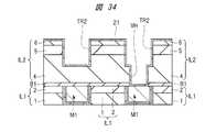
図1は、本実施の形態の半導体装置の要部断面図である。 FIG. 1 is a cross-sectional view of a main part of the semiconductor device of the present embodiment.
図1では、図面の簡略化のために、配線M1が形成された配線層よりも下層の構造については、図示を省略し、また、バリア絶縁膜B2よりも上層の構造も、図示を省略している。 In FIG. 1, for simplification of the drawing, the illustration of the structure below the wiring layer in which the wiring M1 is formed is omitted, and the illustration of the structure above the barrier insulating film B2 is also omitted. ing.
本実施の形態の半導体装置は、半導体基板(後述の半導体基板SBに対応)上に、複数の配線層を有する配線構造(多層配線構造)が形成された半導体装置であり、その配線構造に埋込銅配線が形成されている。 The semiconductor device of the present embodiment is a semiconductor device in which a wiring structure (multilayer wiring structure) having a plurality of wiring layers is formed on a semiconductor substrate (corresponding to a semiconductor substrate SB described later), and is embedded in the wiring structure. Embedded copper wiring is formed.
以下、図1を参照して、本実施の形態の半導体装置について具体的に説明する。 Hereinafter, the semiconductor device of the present embodiment will be specifically described with reference to FIG.
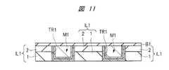
本実施の形態の半導体装置は、半導体基板(後述の半導体基板SBに対応)と、半導体基板(SB)上に形成されかつ複数の配線層を含む配線構造とを有している。この配線構造は、層間絶縁膜IL1と、層間絶縁膜IL1に埋め込まれた配線M1と、層間絶縁膜IL1上に配線M1を覆うように形成されたバリア絶縁膜B1と、バリア絶縁膜B1上に形成された層間絶縁膜IL2と、層間絶縁膜IL2に埋め込まれた配線M2と、層間絶縁膜IL2上に配線M2を覆うように形成されたバリア絶縁膜B2と、を含んでいる。 The semiconductor device of the present embodiment includes a semiconductor substrate (corresponding to a semiconductor substrate SB described later) and a wiring structure formed on the semiconductor substrate (SB) and including a plurality of wiring layers. This wiring structure includes an interlayer insulating film IL1, a wiring M1 embedded in the interlayer insulating film IL1, a barrier insulating film B1 formed on the interlayer insulating film IL1 so as to cover the wiring M1, and a barrier insulating film B1. The interlayer insulating film IL2 formed, the wiring M2 embedded in the interlayer insulating film IL2, and the barrier insulating film B2 formed on the interlayer insulating film IL2 so as to cover the wiring M2 are included.
すなわち、本実施の形態の半導体装置は、半導体基板(後述の半導体基板SBに対応)の上方に形成された層間絶縁膜IL1と、層間絶縁膜IL1に埋め込まれた配線M1と、層間絶縁膜IL1上に配線M1を覆うように形成されたバリア絶縁膜B1と、バリア絶縁膜B1上に形成された層間絶縁膜IL2と、層間絶縁膜IL2に埋め込まれた配線M2と、を有している。 That is, the semiconductor device of this embodiment includes an interlayer insulating film IL1 formed above a semiconductor substrate (corresponding to a semiconductor substrate SB described later), a wiring M1 embedded in the interlayer insulating film IL1, and an interlayer insulating film IL1. It has a barrier insulating film B1 formed so as to cover the wiring M1, an interlayer insulating film IL2 formed on the barrier insulating film B1, and a wiring M2 embedded in the interlayer insulating film IL2.
また、層間絶縁膜IL2上には、配線M2を覆うようにバリア絶縁膜B2が形成されている。バリア絶縁膜B2上には、更に層間絶縁膜や配線などを形成することができるが、ここではその図示および説明は省略する。 A barrier insulating film B2 is formed on the interlayer insulating film IL2 so as to cover the wiring M2. An interlayer insulating film, wiring, and the like can be further formed on the barrier insulating film B2, but illustration and description thereof are omitted here.
配線M1は、配線構造を構成する複数の配線層のうち任意の配線層の配線であり、配線M2は、配線M1が形成された配線層よりも1つ上層の配線層の配線である。 The wiring M1 is a wiring in an arbitrary wiring layer among a plurality of wiring layers constituting the wiring structure, and the wiring M2 is a wiring in a wiring layer one layer higher than the wiring layer in which the wiring M1 is formed.
層間絶縁膜IL1には、少なくとも1つの配線M1が埋め込まれており、実際には、複数の配線M1が埋め込まれている。また、層間絶縁膜IL2には、少なくとも1つの配線M2が埋め込まれており、実際には複数の配線M2が埋め込まれている。 In the interlayer insulating film IL1, at least one wiring M1 is embedded, and actually, a plurality of wirings M1 are embedded. Further, at least one wiring M2 is embedded in the interlayer insulating film IL2, and actually a plurality of wirings M2 are embedded.
配線M1は、層間絶縁膜IL1に形成された配線溝TR1に埋め込まれており、ダマシン法により形成されたダマシン配線(ダマシン埋込配線)である。また、配線M2は、層間絶縁膜IL2に形成された配線溝TR2に埋め込まれており、ダマシン法により形成されたダマシン配線(ダマシン埋込配線)である。また、配線M1,M2は、いずれも、銅を主体(主成分)とする銅配線である。従って、配線M1と配線M2は、いずれも銅を主体(主成分)とするダマシン配線(ダマシン銅配線、埋込銅配線)である。 The wiring M1 is a damascene wiring (damascene embedded wiring) that is embedded in the wiring trench TR1 formed in the interlayer insulating film IL1 and formed by the damascene method. Further, the wiring M2 is a damascene wiring (damascene embedded wiring) formed by a damascene method, embedded in the wiring trench TR2 formed in the interlayer insulating film IL2. The wirings M1 and M2 are both copper wirings mainly composed of copper (main component). Accordingly, the wiring M1 and the wiring M2 are both damascene wiring (damascene copper wiring, embedded copper wiring) mainly composed of copper (main component).
配線M2は、デュアルダマシン法により形成されたデュアルダマシン配線である。また、図1の場合は、配線M1は、配線構造における第1層目(最下層)の配線層の配線の場合が示されており、配線M1はシングルダマシン法により形成されたシングルダマシン配線であるが、配線M1は、配線構造における第1層目の配線層よりも上層の配線層の配線であってもよく、また、配線M1は、デュアルダマシン法により形成されたデュアルダマシン配線であってもよい。 The wiring M2 is a dual damascene wiring formed by a dual damascene method. In the case of FIG. 1, the wiring M1 is a wiring in the first layer (lowermost layer) wiring layer in the wiring structure, and the wiring M1 is a single damascene wiring formed by a single damascene method. However, the wiring M1 may be a wiring in an upper wiring layer than the first wiring layer in the wiring structure, and the wiring M1 is a dual damascene wiring formed by a dual damascene method. Also good.
バリア絶縁膜B1,B2は、銅配線のバリア絶縁膜として機能する。すなわち、バリア絶縁膜B1は、配線M1のバリア絶縁膜として機能し、バリア絶縁膜B2は、配線M2のバリア絶縁膜として機能する。具体的には、バリア絶縁膜B1は、配線M1中の銅(Cu)がバリア絶縁膜B1上に形成された層間絶縁膜(ここでは層間絶縁膜IL2)中に拡散するのを抑制または防止するバリア絶縁膜として機能する。また、バリア絶縁膜B2は、配線M2中の銅(Cu)がバリア絶縁膜B2上に形成された層間絶縁膜(ここでは図示せず)中に拡散するのを抑制または防止するバリア絶縁膜として機能する。 The barrier insulating films B1 and B2 function as barrier insulating films for copper wiring. That is, the barrier insulating film B1 functions as a barrier insulating film for the wiring M1, and the barrier insulating film B2 functions as a barrier insulating film for the wiring M2. Specifically, the barrier insulating film B1 suppresses or prevents diffusion of copper (Cu) in the wiring M1 into an interlayer insulating film (here, the interlayer insulating film IL2) formed on the barrier insulating film B1. Functions as a barrier insulating film. The barrier insulating film B2 is a barrier insulating film that suppresses or prevents diffusion of copper (Cu) in the wiring M2 into an interlayer insulating film (not shown here) formed on the barrier insulating film B2. Function.
このため、バリア絶縁膜B1,B2としては、銅(Cu)に対するバリア性に優れた(銅の拡散を抑制または防止する機能が高い)材料膜を用いることが好ましい。また、バリア絶縁膜B1は、バリア絶縁膜B1上の層間絶縁膜(ここでは層間絶縁膜IL2)にビアホール(ここではビアホールVH)を形成するエッチング工程で、エッチングストッパとして機能することもできる。同様に、バリア絶縁膜B2は、バリア絶縁膜B2上の層間絶縁膜(ここでは図示せず)にビアホールを形成するエッチング工程で、エッチングストッパとして機能することもできる。 For this reason, as the barrier insulating films B1 and B2, it is preferable to use a material film excellent in barrier properties against copper (Cu) (having a high function of suppressing or preventing copper diffusion). The barrier insulating film B1 can also function as an etching stopper in an etching process for forming a via hole (here, the via hole VH) in the interlayer insulating film (here, the interlayer insulating film IL2) over the barrier insulating film B1. Similarly, the barrier insulating film B2 can also function as an etching stopper in an etching process for forming a via hole in an interlayer insulating film (not shown here) on the barrier insulating film B2.
また、バリア絶縁膜B1を、複数の絶縁膜からなる積層膜により形成することも可能である。また、バリア絶縁膜B2を、複数の絶縁膜からなる積層膜により形成することも可能である。 In addition, the barrier insulating film B1 can be formed of a stacked film including a plurality of insulating films. In addition, the barrier insulating film B2 can be formed of a stacked film including a plurality of insulating films.
このため、バリア絶縁膜B1は、例えば、SiN膜(窒化シリコン膜)、SiC膜(炭化シリコン膜)、SiCN膜(炭窒化シリコン膜、窒素添加炭化シリコン膜)、およびSiCO膜(酸炭化シリコン膜、酸素添加炭化シリコン膜)から選択した一層以上により形成することができる。同様に、バリア絶縁膜B2も、例えば、SiN膜(窒化シリコン膜)、SiC膜(炭化シリコン膜)、SiCN膜(炭窒化シリコン膜、窒素添加炭化シリコン膜)、およびSiCO膜(酸炭化シリコン膜、酸素添加炭化シリコン膜)から選択した一層以上により形成することができる。一例を挙げれば、バリア絶縁膜B1,B2のそれぞれは、SiCN膜とその上のSiCO膜との積層膜を用いることができる。 Therefore, the barrier insulating film B1 includes, for example, a SiN film (silicon nitride film), a SiC film (silicon carbide film), a SiCN film (silicon carbonitride film, nitrogen-added silicon carbide film), and a SiCO film (silicon oxycarbide film). , An oxygen-added silicon carbide film). Similarly, the barrier insulating film B2 is, for example, a SiN film (silicon nitride film), a SiC film (silicon carbide film), a SiCN film (silicon carbonitride film, nitrogen-added silicon carbide film), and a SiCO film (silicon oxycarbide film). , An oxygen-added silicon carbide film). As an example, each of the barrier insulating films B1 and B2 can be a laminated film of a SiCN film and a SiCO film thereon.
また、層間絶縁膜IL1,IL2は、いずれも低誘電率絶縁膜からなる。なお、低誘電率絶縁膜とは、酸化シリコン(たとえばTEOS(Tetraethoxysilane)酸化膜)よりも誘電率(比誘電率)が低い絶縁膜を意味する。また、低誘電率絶縁膜を、Low−k膜またはLow−k絶縁膜と称する場合もある。以下では、低誘電率絶縁膜を、Low−k膜と称しており、ポーラスLow−k膜は、ポーラス低誘電率絶縁膜を意味している。 The interlayer insulating films IL1 and IL2 are both made of a low dielectric constant insulating film. The low dielectric constant insulating film means an insulating film having a dielectric constant (relative dielectric constant) lower than that of silicon oxide (for example, TEOS (Tetraethoxysilane) oxide film). The low dielectric constant insulating film may be referred to as a low-k film or a low-k insulating film. Hereinafter, the low dielectric constant insulating film is referred to as a Low-k film, and the porous Low-k film means a porous low dielectric constant insulating film.
層間絶縁膜IL1として低誘電率絶縁膜を用いることで、隣り合う配線M1間の寄生容量を低減することができる。また、層間絶縁膜IL2として低誘電率絶縁膜を用いることで、隣り合う配線M2間の寄生容量を低減することができる。また、配線M2と配線M1との間の寄生容量を低減することもできる。 By using the low dielectric constant insulating film as the interlayer insulating film IL1, the parasitic capacitance between the adjacent wirings M1 can be reduced. Further, by using a low dielectric constant insulating film as the interlayer insulating film IL2, the parasitic capacitance between the adjacent wirings M2 can be reduced. In addition, parasitic capacitance between the wiring M2 and the wiring M1 can be reduced.
すなわち、バリア絶縁膜B1,B2の材料としては、バリア絶縁膜の機能(例えば銅の拡散防止など)に相応しい材料を選択し、一方、層間絶縁膜IL1,IL2の材料としては、配線間の寄生容量を低減させるために、誘電率が低い材料を選択することで、配線構造の、ひいてはその配線構造を有する半導体装置の、信頼性や性能を向上させることができる。 That is, as the material of the barrier insulating films B1 and B2, a material suitable for the function of the barrier insulating film (for example, prevention of copper diffusion) is selected. On the other hand, the material of the interlayer insulating films IL1 and IL2 is parasitic between wirings. By selecting a material having a low dielectric constant in order to reduce the capacitance, the reliability and performance of the wiring structure, and thus the semiconductor device having the wiring structure, can be improved.
このため、層間絶縁膜IL1,IL2の誘電率は、バリア絶縁膜B1,B2の誘電率よりも低い。言い換えると、バリア絶縁膜B1,B2の誘電率は、層間絶縁膜IL1,IL2の誘電率よりも高い。 For this reason, the dielectric constants of the interlayer insulating films IL1 and IL2 are lower than the dielectric constants of the barrier insulating films B1 and B2. In other words, the dielectric constants of the barrier insulating films B1 and B2 are higher than the dielectric constants of the interlayer insulating films IL1 and IL2.
また、本実施の形態では、層間絶縁膜IL1,IL2用の低誘電率絶縁膜として、ポーラスLow−k膜(ポーラス低誘電率絶縁膜、多孔質低誘電率絶縁膜)を用いている。ポーラスLow−k膜は、膜内に多数(複数)の空孔(ポア)を有した多孔質構造を備えており、誘電率の更なる低下が可能であるため、低誘電率絶縁膜として優れている。ポーラスLow−k膜は、他の低誘電率絶縁膜(SiOC膜など)よりも誘電率を低くすることができるため、ポーラスLow−k膜を、ポーラスULK(Ultra Low-k)膜またはポーラスELK(Extreem Low-k)膜と称する場合もある。ポーラスLow−k膜としては、ポーラスSiOC膜などを好適に用いることができる。ポーラスSiOC膜は、膜内に多数(複数)の空孔(ポア)を有した多孔質構造を備えたSiOC膜である。 In this embodiment, a porous Low-k film (porous low dielectric constant insulating film, porous low dielectric constant insulating film) is used as the low dielectric constant insulating film for the interlayer insulating films IL1 and IL2. The porous low-k film has a porous structure having a large number (a plurality) of pores (pores) in the film, and can further lower the dielectric constant, and thus is excellent as a low dielectric constant insulating film. ing. Since the porous low-k film can have a dielectric constant lower than that of other low dielectric constant insulating films (such as SiOC films), the porous low-k film is replaced with a porous ULK (Ultra Low-k) film or a porous ELK. Sometimes referred to as (Extreem Low-k) film. As the porous Low-k film, a porous SiOC film or the like can be preferably used. The porous SiOC film is a SiOC film having a porous structure having a large number (a plurality) of pores (pores) in the film.
層間絶縁膜IL1,IL2として、ポーラスLow−k膜の単層膜を用いることもできるが、ポーラスLow−k膜を含む積層膜(積層絶縁膜)を用いることも可能である。 As the interlayer insulating films IL1 and IL2, a single layer film of a porous Low-k film can be used, but a stacked film (laminated insulating film) including a porous Low-k film can also be used.
ポーラスLow−k膜は、ポーラスであるために、誘電率を低くすることができるが、機械的強度は弱くなる。このため、層間絶縁膜IL1,IL2として、ポーラスLow−k膜の単層膜ではなく、ポーラスLow−k膜とその上の他の絶縁膜との積層膜を用いることで、ダマシン配線を形成する際のCMP処理に対する層間絶縁膜IL1,IL2の耐性を高めることができ、半導体装置の信頼性を高めることができる。 Since the porous Low-k film is porous, the dielectric constant can be lowered, but the mechanical strength is weakened. Therefore, a damascene wiring is formed by using a laminated film of a porous Low-k film and another insulating film thereon instead of a single layer film of a porous Low-k film as the interlayer insulating films IL1 and IL2. The resistance of the interlayer insulating films IL1 and IL2 with respect to the CMP process at the time can be increased, and the reliability of the semiconductor device can be increased.
このため、層間絶縁膜IL1,IL2において、ポーラスLow−k膜上に形成する絶縁膜としては、ポーラスLow−k膜よりも機械的強度が高く、CMP処理に対する耐性が高い絶縁膜を用いることが好ましく、例えば、SiOC膜(ポーラスではないSiOC膜)を用いることができる。SiOC膜は、酸化シリコンに炭素を添加した材料膜(炭素添加酸化シリコン膜)であり、CVD(Chemical Vapor Deposition:化学的気相成長)法などを用いて形成することができる。SiOC膜は、ポーラスLow−k膜よりも誘電率が高いが、酸化シリコンよりも誘電率が低い低誘電率絶縁膜である。このため、層間絶縁膜IL1,IL2として、ポーラスLow−k膜とその上のSiOC膜との積層膜を用いることで、層間絶縁膜IL1,IL2の誘電率を低くすることができるとともに、層間絶縁膜IL1,IL2のCMP処理に対する耐性を向上させることができる。 For this reason, in the interlayer insulating films IL1 and IL2, as the insulating film formed on the porous Low-k film, an insulating film having higher mechanical strength and higher resistance to the CMP process than the porous Low-k film should be used. Preferably, for example, a SiOC film (non-porous SiOC film) can be used. The SiOC film is a material film obtained by adding carbon to silicon oxide (carbon-added silicon oxide film), and can be formed using a CVD (Chemical Vapor Deposition) method or the like. The SiOC film is a low dielectric constant insulating film having a dielectric constant higher than that of the porous Low-k film but lower than that of silicon oxide. For this reason, by using a laminated film of the porous Low-k film and the SiOC film thereon as the interlayer insulating films IL1 and IL2, the dielectric constant of the interlayer insulating films IL1 and IL2 can be lowered, and the interlayer insulating film Resistance to CMP treatment of the films IL1 and IL2 can be improved.
また、層間絶縁膜IL1,IL2を構成する積層膜の最上層の膜を、酸化シリコン膜とすることもできる。例えば、層間絶縁膜IL1,IL2を、ポーラスLow−k膜とその上のSiOC膜とその上の酸化シリコン膜との積層膜とすることができる。酸化シリコン膜は、機械的強度が高く、CMP処理に対する耐性が高い。このため、層間絶縁膜IL1,IL2を構成する積層膜の最上層の膜を、酸化シリコン膜とすることで、層間絶縁膜IL1,IL2のCMP処理に対する耐性を更に向上させることができる。 Further, the uppermost film of the laminated film constituting the interlayer insulating films IL1 and IL2 can be a silicon oxide film. For example, the interlayer insulating films IL1 and IL2 can be a laminated film of a porous Low-k film, a SiOC film thereon, and a silicon oxide film thereon. A silicon oxide film has high mechanical strength and high resistance to CMP treatment. For this reason, the uppermost layer of the laminated film constituting the interlayer insulating films IL1 and IL2 is a silicon oxide film, whereby the resistance of the interlayer insulating films IL1 and IL2 to the CMP process can be further improved.
図1の場合は、層間絶縁膜IL1が、ポーラスLow−k膜1とポーラスLow−k膜1上のSiOC膜2との積層膜であり、層間絶縁膜IL2が、ポーラスLow−k膜4とポーラスLow−k膜4上のSiOC膜5との積層膜である場合が示されている。ポーラスLow−k膜1,4としては、ポーラスSiOC膜を好適に用いることができる。 In the case of FIG. 1, the interlayer insulating film IL1 is a laminated film of the porous Low-
配線M1は、配線溝TR1の内面(底面および側壁)上に形成されたバリア導体膜BR1と、バリア導体膜BR1上に形成されて配線溝TR1を埋め込む主導体膜MC1とにより形成されている。また、配線M2は、配線溝TR2の内面(底面および側壁)上に形成されたバリア導体膜BR2と、バリア導体膜BR2上に形成されて配線溝TR2を埋め込む主導体膜MC2とにより形成されている。 The wiring M1 is formed of a barrier conductor film BR1 formed on the inner surface (bottom surface and side wall) of the wiring groove TR1, and a main conductor film MC1 formed on the barrier conductor film BR1 and burying the wiring groove TR1. The wiring M2 is formed by a barrier conductor film BR2 formed on the inner surface (bottom surface and side wall) of the wiring groove TR2, and a main conductor film MC2 formed on the barrier conductor film BR2 and burying the wiring groove TR2. Yes.
主導体膜MC1,MC2は、銅(Cu)を主成分とする導電膜(但し金属伝導を示す導電膜)である。このため、配線M1,M2は、銅配線とみなすことができる。主導体膜MC1,MC2としては、銅(Cu)膜または銅(Cu)合金膜あるいは銅(Cu)化合物膜を好適に用いることができる。但し、銅合金膜または銅化合物を用いる場合は、銅(Cu)リッチな銅合金膜または銅化合物膜が好ましい。ここで、銅(Cu)リッチとは、銅(Cu)の組成比が50原子%より大きいことを意味する。 The main conductor films MC1 and MC2 are conductive films containing copper (Cu) as a main component (however, conductive films exhibiting metal conduction). Therefore, the wirings M1 and M2 can be regarded as copper wirings. As the main conductor films MC1 and MC2, a copper (Cu) film, a copper (Cu) alloy film, or a copper (Cu) compound film can be suitably used. However, when a copper alloy film or a copper compound is used, a copper (Cu) rich copper alloy film or a copper compound film is preferable. Here, copper (Cu) rich means that the composition ratio of copper (Cu) is larger than 50 atomic%.
バリア導体膜BR1は、主導体膜MC1中の銅(Cu)が層間絶縁膜IL1中に拡散するのを抑制または防止するバリア導体膜として機能する。また、バリア導体膜BR1は、配線M1と層間絶縁膜IL1との密着性を向上させる機能も有している。また、バリア導体膜BR2は、主導体膜MC2中の銅(Cu)が層間絶縁膜IL2中に拡散するのを抑制または防止するバリア導体膜として機能する。また、バリア導体膜BR2は、配線M2と層間絶縁膜IL2との密着性を向上させる機能も有している。 The barrier conductor film BR1 functions as a barrier conductor film that suppresses or prevents copper (Cu) in the main conductor film MC1 from diffusing into the interlayer insulating film IL1. The barrier conductor film BR1 also has a function of improving the adhesion between the wiring M1 and the interlayer insulating film IL1. The barrier conductor film BR2 functions as a barrier conductor film that suppresses or prevents copper (Cu) in the main conductor film MC2 from diffusing into the interlayer insulating film IL2. The barrier conductor film BR2 also has a function of improving the adhesion between the wiring M2 and the interlayer insulating film IL2.
バリア導体膜BR1は、複数のバリア導体膜を積層した積層構造を有している。具体的には、バリア導体膜BR1は、3層のバリア導体膜により形成されており、最下層のバリア導体膜11と、中間層のバリア導体膜12と、最上層のバリア導体膜13との積層膜からなる。つまり、バリア導体膜BR1は、バリア導体膜11と、バリア導体膜11上のバリア導体膜12と、バリア導体膜12上のバリア導体膜13との積層膜からなる。 The barrier conductor film BR1 has a laminated structure in which a plurality of barrier conductor films are laminated. Specifically, the barrier conductor film BR1 is formed of three layers of barrier conductor films, and includes a lowermost
バリア導体膜BR1の最下層のバリア導体膜11は、配線溝TR1の内面(底面および側壁)上に形成されている。このため、バリア導体膜11は、配線溝TR1の側壁において、層間絶縁膜IL1(ここではポーラスLow−k膜1およびSiOC膜2)に接している。バリア導体膜12と配線溝TR1の内面(底面および側壁)との間には、バリア導体膜11が介在しており、従って、バリア導体膜12と層間絶縁膜IL1との間には、バリア導体膜11が介在している。バリア導体膜13とバリア導体膜11との間には、バリア導体膜12が介在し、主導体膜MC1とバリア導体膜12との間には、バリア導体膜13が介在している。 The lowermost
バリア導体膜BR1を構成するバリア導体膜11とバリア導体膜12とは、同じ導体材料からなり、好ましくは窒化タンタル(TaN)からなる。このため、バリア導体膜11とバリア導体膜12とは、いずれも、窒化タンタル(TaN)膜からなることが好ましい。 The
バリア導体膜11の密度は、バリア導体膜12の密度よりも低い。言い換えると、バリア導体膜12の密度は、バリア導体膜11の密度よりも高い。従って、バリア導体膜11は、好ましくは低密度窒化タンタル膜であり、バリア導体膜12は、好ましくは高密度窒化タンタル膜である。 The density of the
一方、バリア導体膜BR1を構成するバリア導体膜13は、バリア導体膜11,12とは異なる導体材料からなり、好ましくはタンタル(Ta)からなる。このため、バリア導体膜13は、好ましくはタンタル(Ta)膜である。 On the other hand, the
また、バリア導体膜BR2は、複数のバリア導体膜を積層した積層構造を有している。具体的には、バリア導体膜BR2は、3層のバリア導体膜により形成されており、最下層のバリア導体膜21と、中間層のバリア導体膜22と、最上層のバリア導体膜23との積層膜からなる。つまり、バリア導体膜BR2は、バリア導体膜21と、バリア導体膜21上のバリア導体膜22と、バリア導体膜22上のバリア導体膜23との積層膜からなる。 The barrier conductor film BR2 has a laminated structure in which a plurality of barrier conductor films are laminated. Specifically, the barrier conductor film BR2 is formed of three layers of barrier conductor films, and includes a lowermost
バリア導体膜BR2の最下層のバリア導体膜21は、配線溝TR2の内面(底面および側壁)上とビアホールVHの内面(底面および側壁)上とに形成されている。このため、バリア導体膜21は、配線溝TR2の側壁において、層間絶縁膜IL2(ここではポーラスLow−k膜4およびSiOC膜5の側面)に接し、配線溝TR2の底面において、層間絶縁膜IL2(ここではポーラスLow−k膜4)に接し、ビアホールVHの側壁において、層間絶縁膜IL2(ここではポーラスLow−k膜4)に接している。バリア導体膜22と配線溝TR2およびビアホールVHの内面(底面および側壁)との間には、バリア導体膜21が介在しており、従って、バリア導体膜22と層間絶縁膜IL2との間には、バリア導体膜21が介在している。バリア導体膜23とバリア導体膜21との間には、バリア導体膜22が介在し、主導体膜MC2とバリア導体膜22との間には、バリア導体膜23が介在している。 The lowermost
バリア導体膜BR2を構成するバリア導体膜21とバリア導体膜22とは、同じ導体材料からなり、好ましくは窒化タンタル(TaN)からなる。このため、バリア導体膜21とバリア導体膜22とは、いずれも、窒化タンタル(TaN)膜からなることが好ましい。 The
バリア導体膜21の密度は、バリア導体膜22の密度よりも低い。言い換えると、バリア導体膜22の密度は、バリア導体膜21の密度よりも高い。従って、バリア導体膜21は、好ましくは低密度窒化タンタル膜であり、バリア導体膜22は、好ましくは高密度窒化タンタル膜である。 The density of the
一方、バリア導体膜BR2を構成するバリア導体膜23は、バリア導体膜21,22とは異なる導体材料からなり、好ましくはタンタル(Ta)からなる。このため、バリア導体膜23は、好ましくはタンタル(Ta)膜である。 On the other hand, the
配線M2の下面は、層間絶縁膜IL2の厚みの途中に位置している。すなわち、層間絶縁膜IL2に形成された配線溝TR2に配線M2が埋め込まれているが、配線溝TR2の底面(ビアホールVHを除く)は、層間絶縁膜IL2の厚みの途中に位置している。つまり、ビアホールVHは層間絶縁膜IL2とバリア絶縁膜B1とを貫通しているが、配線溝TR2は層間絶縁膜IL2を貫通しておらず、配線溝TR2の底面は、層間絶縁膜IL2の厚みの途中に位置している。ここでは、配線溝TR2の底面は、ポーラスLow−k膜4の厚みの途中に位置している。このため、配線M2のビア部(ビアホールVHを埋め込む部分)を除き、配線M2の下面とバリア絶縁膜B1の上面との間には、層間絶縁膜IL2の一部(ここではポーラスLow−k膜4の一部)が介在している。 The lower surface of the wiring M2 is located in the middle of the thickness of the interlayer insulating film IL2. That is, the wiring M2 is embedded in the wiring trench TR2 formed in the interlayer insulating film IL2, but the bottom surface (except for the via hole VH) of the wiring trench TR2 is located in the middle of the thickness of the interlayer insulating film IL2. That is, the via hole VH penetrates the interlayer insulating film IL2 and the barrier insulating film B1, but the wiring trench TR2 does not penetrate the interlayer insulating film IL2, and the bottom surface of the wiring trench TR2 is the thickness of the interlayer insulating film IL2. Located in the middle of Here, the bottom surface of the wiring trench TR <b> 2 is located in the middle of the thickness of the porous Low-
配線M2は、配線M2のビア部(ビアホールVHを埋め込む部分)を介して、配線M1と電気的に接続されている。配線M2のビア部は、配線M2のうち、ビアホールVHを埋め込む部分に対応している。ビアホール(孔部)VHは、配線溝TR2に平面視で内包されるように形成されており、ビアホールVHは、層間絶縁膜IL2とバリア絶縁膜B1とを貫通し、ビアホールVHの底面(底部)では、配線M1の上面が露出されている。このため、配線M2は、配線溝TR2内に埋め込まれているが、配線M2のビア部は、ビアホールVH内に埋め込まれている。配線M2は、デュアルダマシン配線であるため、配線M2のビア部(ビアホールVHを埋め込む部分)は、その配線M2(配線溝TR2に埋め込まれた配線M2)と一体的に形成されている。配線M2のビア部は、配線M1の上面に接してその配線M1に電気的に接続されている。これにより、配線M2を配線M2のビア部を介して、配線M1と電気的に接続することができる。 The wiring M2 is electrically connected to the wiring M1 through a via portion (a portion where the via hole VH is embedded) of the wiring M2. The via portion of the wiring M2 corresponds to a portion of the wiring M2 in which the via hole VH is embedded. The via hole (hole part) VH is formed so as to be included in the wiring trench TR2 in a plan view. The via hole VH penetrates the interlayer insulating film IL2 and the barrier insulating film B1, and the bottom surface (bottom part) of the via hole VH. Then, the upper surface of the wiring M1 is exposed. For this reason, the wiring M2 is embedded in the wiring trench TR2, but the via portion of the wiring M2 is embedded in the via hole VH. Since the wiring M2 is a dual damascene wiring, the via portion (portion where the via hole VH is embedded) of the wiring M2 is formed integrally with the wiring M2 (wiring M2 embedded in the wiring trench TR2). The via portion of the wiring M2 is in contact with the upper surface of the wiring M1 and is electrically connected to the wiring M1. Thus, the wiring M2 can be electrically connected to the wiring M1 via the via portion of the wiring M2.
<半導体装置の製造方法について>
次に、本実施の形態の半導体装置の製造工程を、図2〜図24を参照して説明する。図2〜図24は、本実施の形態の半導体装置の製造工程中の要部断面図である。<About manufacturing method of semiconductor device>
Next, the manufacturing process of the semiconductor device according to the present embodiment will be described with reference to FIGS. 2 to 24 are main-portion cross-sectional views during the manufacturing process of the semiconductor device of the present embodiment.
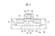
まず、図2に示されるように、例えば1〜10Ωcm程度の比抵抗を有するp型の単結晶シリコンなどからなる半導体基板(半導体ウエハ)SBを準備する。 First, as shown in FIG. 2, a semiconductor substrate (semiconductor wafer) SB made of p-type single crystal silicon having a specific resistance of, for example, about 1 to 10 Ωcm is prepared.
次に、半導体基板SBに素子分離領域STを形成する。素子分離領域STは、STI(Shallow Trench Isolation)法により形成することができる。 Next, the element isolation region ST is formed in the semiconductor substrate SB. The element isolation region ST can be formed by an STI (Shallow Trench Isolation) method.
次に、半導体基板SBに、nチャネル型のMISFET(Metal Insulator Semiconductor Field Effect Transistor)10などの半導体素子を形成する。MISFET10は、例えば次のようにして形成することができる。 Next, a semiconductor element such as an n-channel MISFET (Metal Insulator Semiconductor Field Effect Transistor) 10 is formed on the semiconductor substrate SB. The
すなわち、半導体基板SBにp型ウエルPWをイオン注入法などを用いて形成する。それから、p型ウエルPW上に、ゲート絶縁膜GFを介してnチャネル型のMISFET10用のゲート電極GEを形成する。それから、ゲート電極GEをマスクとして用いてp型ウエルPWにn型不純物をイオン注入することにより、p型ウエルPWにおいて、ゲート電極GEの両側にn−型半導体領域EXを形成する。それから、ゲート電極GEの側壁上にサイドウォールスペーサ(側壁絶縁膜)SWを形成する。それから、ゲート電極GEおよびサイドウォールスペーサSWをマスクとして用いてp型ウエルPWにn型不純物をイオン注入することにより、p型ウエルPWにおいて、ゲート電極GEおよびサイドウォールスペーサSWからなる構造体の両側に、n−型半導体領域EXよりも高不純物濃度のn+型半導体領域SDを形成する。n−型半導体領域EXおよびn+型半導体領域SDにより、nチャネル型のMISFET10のLDD(lightly doped drain)構造を有するソース・ドレイン領域が形成される。その後、これまでに導入した不純物を活性化させるための熱処理である活性化アニールを行う。また、ゲート電極GEおよびn+型半導体領域SDの表層部分に、サリサイド(Salicide:Self Aligned Silicide)技術などにより、それぞれ金属シリサイド層SLを形成することもできる。That is, the p-type well PW is formed in the semiconductor substrate SB using an ion implantation method or the like. Then, the gate electrode GE for the n-
このようにして、半導体基板SBに、nチャネル型のMISFET10を形成することができる。 In this way, the n-
なお、ここでは、一例として、半導体基板SBに半導体素子としてnチャネル型のMISFETを形成する場合について説明したが、導電型を反対にして、半導体基板SBにpチャネル型のMISFETを形成することもでき、あるいは、半導体基板SBにnチャネル型のMISFETとpチャネル型のMISFETとの両方を形成することもできる。また、半導体基板SBに形成する半導体素子は、MISFETに限定されず、種々の半導体素子を半導体基板SBに形成することができる。 Here, as an example, the case where an n-channel MISFET is formed as a semiconductor element on the semiconductor substrate SB has been described. However, a p-channel MISFET may be formed on the semiconductor substrate SB with the conductivity type reversed. Alternatively, both an n-channel MISFET and a p-channel MISFET can be formed on the semiconductor substrate SB. The semiconductor element formed on the semiconductor substrate SB is not limited to the MISFET, and various semiconductor elements can be formed on the semiconductor substrate SB.
次に、図3に示されるように、半導体基板SBの主面全面上に、ゲート電極GEおよびサイドウォールスペーサSWを覆うように、層間絶縁膜SOをCVD法などを用いて形成する。層間絶縁膜SOは、例えば、酸化シリコン膜の単体膜、あるいは、窒化シリコン膜と該窒化シリコン膜上の酸化シリコン膜との積層膜などからなる。層間絶縁膜SOの成膜後、層間絶縁膜SOの上面をCMP(Chemical Mechanical Polishing:化学的機械的研磨)法により研磨するなどして、層間絶縁膜SOの上面を平坦化することもできる。 Next, as shown in FIG. 3, an interlayer insulating film SO is formed over the entire main surface of the semiconductor substrate SB using the CVD method or the like so as to cover the gate electrode GE and the sidewall spacer SW. The interlayer insulating film SO is made of, for example, a single film of a silicon oxide film or a laminated film of a silicon nitride film and a silicon oxide film on the silicon nitride film. After the formation of the interlayer insulating film SO, the upper surface of the interlayer insulating film SO can be planarized by polishing the upper surface of the interlayer insulating film SO by a CMP (Chemical Mechanical Polishing) method.
次に、層間絶縁膜SO上にフォトリソグラフィ法を用いてフォトレジストパターン(図示せず)を形成し、このフォトレジストパターンをエッチングマスクとして層間絶縁膜SOをエッチングすることにより、層間絶縁膜SOにコンタクトホールCTを形成する。 Next, a photoresist pattern (not shown) is formed on the interlayer insulating film SO by using a photolithography method, and the interlayer insulating film SO is etched using the photoresist pattern as an etching mask to form the interlayer insulating film SO. A contact hole CT is formed.
次に、コンタクトホールCT内に、導電性のプラグPGを形成する。プラグPGを形成するには、まず、コンタクトホールCTの内面(底面および側壁)上を含む層間絶縁膜SO上に導電性バリア膜(例えばチタン膜、窒化チタン膜、あるいはそれらの積層膜)をスパッタリング法などによって形成した後、タングステン(W)膜などからなる主導体をCVD法などによって導電性バリア膜上にコンタクトホールCTを埋めるように形成する。それから、コンタクトホールCTの外部の不要な主導体膜および導電性バリア膜をCMP法などによって除去する。これにより、コンタクトホールCT内に埋め込まれて残存する主導体膜および導電性バリア膜からなるプラグPGを形成することができる。なお、図面の簡略化のために、図3では、プラグPGを構成するバリア導体膜と主導体膜とを一体化して示してある。 Next, a conductive plug PG is formed in the contact hole CT. In order to form the plug PG, first, a conductive barrier film (for example, a titanium film, a titanium nitride film, or a laminated film thereof) is sputtered on the interlayer insulating film SO including the inner surface (bottom surface and side wall) of the contact hole CT. After forming by a method or the like, a main conductor made of a tungsten (W) film or the like is formed by a CVD method or the like so as to fill the contact hole CT on the conductive barrier film. Then, unnecessary main conductor film and conductive barrier film outside the contact hole CT are removed by CMP or the like. As a result, the plug PG composed of the main conductor film and the conductive barrier film embedded and remaining in the contact hole CT can be formed. For simplification of the drawing, FIG. 3 shows the barrier conductor film and the main conductor film constituting the plug PG in an integrated manner.
次に、図4に示されるように、プラグPGが埋め込まれた層間絶縁膜SO上に、層間絶縁膜IL1を形成する。層間絶縁膜IL1は、ポーラスLow−k膜の単層膜、あるいは、ポーラスLow−k膜を含む積層膜からなる。ここでは、層間絶縁膜IL1は、ポーラスLow−k膜1と、ポーラスLow−k膜1上のSiOC膜2と、SiOC膜2上の酸化シリコン膜3(例えばTEOS酸化膜)との積層膜からなる。 Next, as shown in FIG. 4, an interlayer insulating film IL1 is formed on the interlayer insulating film SO in which the plug PG is embedded. The interlayer insulating film IL1 is formed of a single layer film of a porous Low-k film or a laminated film including a porous Low-k film. Here, the interlayer insulating film IL1 is a laminated film of a porous Low-
次に、層間絶縁膜IL1上にフォトリソグラフィ法を用いてフォトレジストパターン(図示せず)を形成してから、このフォトレジストパターンをエッチングマスクとして層間絶縁膜IL1をエッチングすることにより、図5示されるように、層間絶縁膜IL1に配線溝(溝部、開口部)TR1を形成する。その後、フォトレジストパターンは除去され、図5にはこの段階が示されている。 Next, a photoresist pattern (not shown) is formed on the interlayer insulating film IL1 by using a photolithography method, and then the interlayer insulating film IL1 is etched using the photoresist pattern as an etching mask, as shown in FIG. As shown, a wiring trench (groove, opening) TR1 is formed in the interlayer insulating film IL1. Thereafter, the photoresist pattern is removed, and this stage is shown in FIG.
配線溝TR1の側壁では、層間絶縁膜IL1の側面(ここではポーラスLow−k膜1とSiOC膜2と酸化シリコン膜3の側面)が露出され、配線溝TR1の底面では、層間絶縁膜SOの上面が露出されている。 On the side wall of the wiring trench TR1, the side surface of the interlayer insulating film IL1 (here, the side surface of the porous Low-
次に、ダマシン法(ここではシングルダマシン法)により配線M1を形成するが、具体的には、次のようにして配線M1を形成することができる。 Next, the wiring M1 is formed by a damascene method (here, a single damascene method). Specifically, the wiring M1 can be formed as follows.
まず、図6に示されるように、半導体基板SBの主面上に、すなわち配線溝TR1の内面(底面および側壁)上を含む層間絶縁膜IL1上に、バリア導体膜11を形成する。バリア導体膜11は、好ましくは窒化タンタル(TaN)膜からなり、スパッタリング法またはALD(Atomic Layer Deposition:原子層堆積)法により好適に形成することができる。なお、スパッタリング法は、PVD(Physical Vapor Deposition:物理的気相成長)法とみなすこともできる。 First, as shown in FIG. 6, the
次に、図7に示されるように、バリア導体膜11上に、バリア導体膜12を形成する。バリア導体膜12は、バリア導体膜11と同じ導電材料からなり、ここでは窒化タンタル(TaN)膜からなる。バリア導体膜12は、スパッタリング法により好適に形成することができる。バリア導体膜11とバリア導体膜12とは、同種の導電材料(ここでは窒化タンタル)からなるが、バリア導体膜12の密度は、バリア導体膜11の密度よりも高い。 Next, as shown in FIG. 7, the
次に、図8に示されるように、バリア導体膜12上に、バリア導体膜13を形成する。バリア導体膜13は、バリア導体膜11,12とは異なる導電材料からなり、ここではタンタル(Ta)膜からなる。バリア導体膜13は、スパッタリング法により好適に形成することができる。 Next, as shown in FIG. 8, a
これにより、バリア導体膜11と、バリア導体膜11上のバリア導体膜12と、バリア導体膜12上のバリア導体膜13との積層膜からなるバリア導体膜BR1が、配線溝TR1の内面(底面および側壁)上を含む層間絶縁膜IL1上に形成された状態になる。この段階では、配線溝TR1はまだ埋まっていない。 As a result, the barrier conductor film BR1, which is a laminated film of the
次に、図9に示されるように、バリア導体膜BR1上に、従って、バリア導体膜BR1の最上層のバリア導体膜13上に、配線溝TR1内を埋める(満たす)ように、銅を主成分とする主導体膜MC1を形成する。 Next, as shown in FIG. 9, copper is mainly used to fill (fill) the wiring trench TR1 on the barrier conductor film BR1, and thus on the uppermost
主導体膜MC1は、例えば、バリア導体膜BR1上(従ってバリア導体膜13上)にCVD法またはスパッタリング法などを用いて形成した相対的に薄い銅のシード層と、この銅のシード層上に電解めっき法などを用いて形成した相対的に厚い(シード層よりも厚い)銅めっき膜とからなり、この銅めっき膜により、配線溝TR1内を埋め込むことができる。主導体膜MC1の形成膜厚は、バリア導体膜BR1の形成膜厚よりも厚い。 The main conductor film MC1 is, for example, a relatively thin copper seed layer formed on the barrier conductor film BR1 (and thus on the barrier conductor film 13) by using a CVD method or a sputtering method, and on the copper seed layer. It is made of a relatively thick copper plating film (thicker than the seed layer) formed by using an electrolytic plating method or the like, and the wiring trench TR1 can be filled with this copper plating film. The formation thickness of the main conductor film MC1 is larger than the formation thickness of the barrier conductor film BR1.
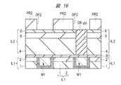
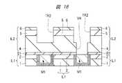
次に、図10に示されるように、配線溝TR1の外部の不要な主導体膜MC1およびバリア導体膜BR1(11,12,13)をCMP法による研磨処理などで除去し、配線溝TR1内に主導体膜MC1およびバリア導体膜BR1(11,12,13)を残すことにより、配線M1を形成する。この際の研磨処理を、以下では図10の研磨処理と称することとする。配線M1は、配線溝TR1内に埋め込まれた主導体膜MC1およびバリア導体膜BR1(11,12,13)からなる。図10の研磨処理を行うと、層間絶縁膜IL1の上面と配線M1の上面とが露出され、層間絶縁膜IL1の露出する上面と配線M1の露出する上面とは、ほぼ平坦な面を形成する。 Next, as shown in FIG. 10, unnecessary main conductor film MC1 and barrier conductor film BR1 (11, 12, 13) outside the wiring trench TR1 are removed by a polishing process or the like by CMP, and the inside of the wiring trench TR1. The wiring M1 is formed by leaving the main conductor film MC1 and the barrier conductor film BR1 (11, 12, 13). The polishing process at this time is hereinafter referred to as the polishing process of FIG. The wiring M1 includes a main conductor film MC1 and a barrier conductor film BR1 (11, 12, 13) embedded in the wiring trench TR1. When the polishing process of FIG. 10 is performed, the upper surface of the interlayer insulating film IL1 and the upper surface of the wiring M1 are exposed, and the exposed upper surface of the interlayer insulating film IL1 and the exposed upper surface of the wiring M1 form a substantially flat surface. .
酸化シリコン膜3は、図10の研磨処理による研磨圧力またはスクラッチダメージなどから、酸化シリコン膜3よりも下の構造を保護するように機能することができる。酸化シリコン膜3は、図10の研磨処理で除去され得る。このため、図10の研磨処理を行うと、SiOC膜2の上面が露出され、SiOC膜2の上面と、配線M1の上面とは、ほぼ平坦な面を形成する。 The
また、図10の研磨処理で酸化シリコン膜3が除去されてSiOC膜2の上面が露出された場合を、図10に示しており、この場合は、図10の研磨処理を行った後は、層間絶縁膜IL1は、ポーラスLow−k膜1とポーラスLow−k膜1上のSiOC膜2との積層膜で構成されることになる。他の形態として、図10の研磨処理において、酸化シリコン膜3が層状に残存する場合もあり得る。その場合は、図10の研磨処理を行った後も、層間絶縁膜IL1は、ポーラスLow−k膜1とポーラスLow−k膜1上のSiOC膜2とSiOC膜2上の酸化シリコン膜3との積層膜で構成されることになる。 FIG. 10 shows a case where the
このようにして、配線M1を形成することができる。 In this way, the wiring M1 can be formed.
なお、以降の図11〜図24では、図面の簡略化のために、層間絶縁膜IL1よりも下の構造については、図示を省略している。 In the following FIGS. 11 to 24, the illustration of the structure below the interlayer insulating film IL1 is omitted for simplification of the drawings.
次に、必要に応じて、配線M1を埋め込んだ層間絶縁膜IL1の表面に対してアンモニアプラズマ処理などを施して、配線M1の上面および層間絶縁膜IL1の上面を清浄化する。 Next, if necessary, the surface of the interlayer insulating film IL1 in which the wiring M1 is embedded is subjected to ammonia plasma treatment or the like to clean the upper surface of the wiring M1 and the upper surface of the interlayer insulating film IL1.
次に、図11に示されるように、配線M1が埋め込まれた層間絶縁膜IL1上に、配線M1を覆うように、バリア絶縁膜B1を形成する。 Next, as shown in FIG. 11, a barrier insulating film B1 is formed on the interlayer insulating film IL1 in which the wiring M1 is embedded so as to cover the wiring M1.
バリア絶縁膜B1は、例えば、SiN膜、SiC膜、SiCN膜、およびSiCO膜から選択した一層以上により形成することができる。一例を挙げれば、バリア絶縁膜B1として、SiCN膜とその上のSiCO膜との積層膜を用いることができる。バリア絶縁膜B1は、CVD法などを用いて形成することができる。 The barrier insulating film B1 can be formed of, for example, one or more layers selected from a SiN film, a SiC film, a SiCN film, and a SiCO film. As an example, a laminated film of a SiCN film and a SiCO film thereon can be used as the barrier insulating film B1. The barrier insulating film B1 can be formed using a CVD method or the like.
次に、図12に示されるように、バリア絶縁膜B1上に、層間絶縁膜IL2を形成する。層間絶縁膜IL2は、ポーラスLow−k膜の単層膜、あるいは、ポーラスLow−k膜を含む積層膜からなる。ここでは、層間絶縁膜IL2は、ポーラスLow−k膜4と、ポーラスLow−k膜4上のSiOC膜5と、SiOC膜5上の酸化シリコン膜6(例えばTEOS酸化膜)との積層膜からなる。 Next, as shown in FIG. 12, an interlayer insulating film IL2 is formed on the barrier insulating film B1. The interlayer insulating film IL2 is composed of a single layer film of a porous Low-k film or a laminated film including a porous Low-k film. Here, the interlayer insulating film IL2 is a laminated film of a porous Low-
次に、層間絶縁膜IL2に、ビアホール(孔部)VHを形成する。ビアホールVHは、例えば次のようにして形成することができる。 Next, a via hole (hole) VH is formed in the interlayer insulating film IL2. The via hole VH can be formed as follows, for example.
まず、図13に示されるように、層間絶縁膜IL2上にフォトリソグラフィ法を用いてフォトレジストパターン(レジストパターン、マスク層)PR1を形成する。フォトレジストパターンPR1は、ビアホールVHを形成する予定領域を露出する開口部OP1を有している。 First, as shown in FIG. 13, a photoresist pattern (resist pattern, mask layer) PR1 is formed on the interlayer insulating film IL2 by using a photolithography method. The photoresist pattern PR1 has an opening OP1 that exposes a region where a via hole VH is to be formed.
それから、フォトレジストパターンPR1をエッチングマスクとして用いて層間絶縁膜IL2をエッチングすることにより、図14に示されるように、層間絶縁膜IL2にビアホールVHを形成する。この際、フォトレジストパターンPR1の開口部OP1から露出する部分の層間絶縁膜IL2がエッチングされてビアホールVHが形成される。層間絶縁膜IL2をエッチングしてビアホールVHを形成する際は、バリア絶縁膜B1をエッチングストッパ膜として機能させることができる。その後、フォトレジストパターンPR1を除去し、図14にはこの段階が示されている。 Then, the interlayer insulating film IL2 is etched using the photoresist pattern PR1 as an etching mask, thereby forming a via hole VH in the interlayer insulating film IL2, as shown in FIG. At this time, the portion of the interlayer insulating film IL2 exposed from the opening OP1 of the photoresist pattern PR1 is etched to form a via hole VH. When the via hole VH is formed by etching the interlayer insulating film IL2, the barrier insulating film B1 can function as an etching stopper film. Thereafter, the photoresist pattern PR1 is removed, and this stage is shown in FIG.
このようにして、層間絶縁膜IL2に、ビアホールVHを形成することができる。この段階でのビアホールVHは、層間絶縁膜IL2を貫通して底面(底部)でバリア絶縁膜B1を露出する。 In this way, the via hole VH can be formed in the interlayer insulating film IL2. The via hole VH at this stage penetrates the interlayer insulating film IL2 and exposes the barrier insulating film B1 at the bottom (bottom).
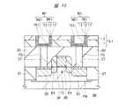
次に、層間絶縁膜IL2に配線溝(溝部)TR2を形成する。配線溝TR2は、例えば次のようにして形成することができる。 Next, a wiring trench (groove portion) TR2 is formed in the interlayer insulating film IL2. The wiring trench TR2 can be formed as follows, for example.
まず、図15に示されるように、ビアホールVH内に絶縁膜CB(ビアフィル材)を埋め込む。この構造は、例えば、ビアホールVH内を埋める(満たす)ように、層間絶縁膜IL2上に絶縁膜CBを形成してから、エッチバックなどにより、ビアホールVHの外部の絶縁膜CBを除去し、ビアホールVH内の絶縁膜CBを残すことにより、得ることができる。絶縁膜CBは、後で選択的に除去しやすい材料により形成することが好ましく、例えばレジスト膜(レジスト材料膜)または有機膜(有機絶縁膜)などからなる。 First, as shown in FIG. 15, an insulating film CB (via fill material) is buried in the via hole VH. In this structure, for example, the insulating film CB is formed on the interlayer insulating film IL2 so as to fill (fill) the via hole VH, and then the insulating film CB outside the via hole VH is removed by etch back or the like, thereby forming the via hole. It can be obtained by leaving the insulating film CB in VH. The insulating film CB is preferably formed of a material that can be easily removed later, and is made of, for example, a resist film (resist material film) or an organic film (organic insulating film).
それから、図16に示されるように、層間絶縁膜IL2上に、フォトリソグラフィ法を用いてフォトレジストパターン(レジストパターン、マスク層)PR2を形成する。フォトレジストパターンPR2は、配線溝TR2を形成する予定領域を露出する開口部OP2を有している。 Then, as shown in FIG. 16, a photoresist pattern (resist pattern, mask layer) PR2 is formed on the interlayer insulating film IL2 by using a photolithography method. The photoresist pattern PR2 has an opening OP2 that exposes a planned region for forming the wiring trench TR2.
それから、フォトレジストパターンPR2をエッチングマスクとして用いて、酸化シリコン膜6をエッチングすることにより、酸化シリコン膜6に溝TR2を形成する。この際、フォトレジストパターンPR2の開口部OP2から露出する部分の酸化シリコン膜6がエッチングされて配線溝TR2が形成される。この際、SiOC膜5をエッチングストッパ膜として機能させることができる。この段階では、配線溝TR2の深さは浅く、配線溝TR2の底面では、SiOC膜5が露出される。 Then, the trench TR2 is formed in the
それから、フォトレジストパターンPR2とビアホールVH内の絶縁膜CBとを除去する。絶縁膜CBを、アッシングによって除去可能な材料(例えばレジスト材料)により形成しておけば、フォトレジストパターンPR2をアッシングによって除去する際に、ビアホールVH内の絶縁膜CBも一緒に除去することができる。 Then, the photoresist pattern PR2 and the insulating film CB in the via hole VH are removed. If the insulating film CB is formed of a material that can be removed by ashing (for example, a resist material), the insulating film CB in the via hole VH can be removed together when the photoresist pattern PR2 is removed by ashing. .
それから、酸化シリコン膜6をエッチングマスク(ハードマスク)として用いて、配線溝TR2の底面のSiOC膜5およびポーラスLow−k膜4をエッチングする。これにより、配線溝TR2の底面の位置が深くなる。但し、配線溝TR2が層間絶縁膜IL2を貫通する前に、エッチングを終了する。図17には、この段階が示されている。 Then, using the
それから、図18に示されるように、ビアホールVHの底面から露出する部分のバリア絶縁膜B1をエッチングにより除去する。これにより、ビアホールVHの底面で配線M1の上面が露出される。 Then, as shown in FIG. 18, the portion of the barrier insulating film B1 exposed from the bottom surface of the via hole VH is removed by etching. As a result, the upper surface of the wiring M1 is exposed at the bottom surface of the via hole VH.
このようにして、配線溝TR2およびビアホールVHが形成される。 In this way, the wiring trench TR2 and the via hole VH are formed.
図18に示されるように、配線溝TR2は、層間絶縁膜IL2を貫通しておらず、配線溝TR2の底面は、層間絶縁膜IL2の厚みの途中、より特定的にはポーラスLow−k膜4の厚みの途中、に位置している。ビアホールVHは、平面視において配線溝TR2に内包されており、層間絶縁膜IL2とバリア絶縁膜B1とを貫通し、ビアホールVHの底面では配線M1の上面が露出されている。 As shown in FIG. 18, the wiring trench TR2 does not penetrate the interlayer insulating film IL2, and the bottom surface of the wiring trench TR2 is in the middle of the thickness of the interlayer insulating film IL2, more specifically, the porous Low-k film. 4 is located in the middle of the thickness. The via hole VH is included in the wiring trench TR2 in plan view, penetrates the interlayer insulating film IL2 and the barrier insulating film B1, and the upper surface of the wiring M1 is exposed at the bottom surface of the via hole VH.
配線溝TR2の側壁では、層間絶縁膜IL2の側面(ここではポーラスLow−k膜4とSiOC膜5と酸化シリコン膜6の側面)が露出され、配線溝TR2の底面では、層間絶縁膜IL2(ここではポーラスLow−k膜4)が露出されている。また、ビアホールVHの側壁では、層間絶縁膜IL2の側面(ここではポーラスLow−k膜4の側面)が露出され、ビアホールVHの底面では、配線M1の上面が露出されている。 On the side wall of the wiring trench TR2, the side surface of the interlayer insulating film IL2 (here, the side surface of the porous Low-
次に、ダマシン法(ここではデュアルダマシン法)により配線M2を形成するが、具体的には、次のようにして配線M2を形成することができる。 Next, the wiring M2 is formed by the damascene method (here, the dual damascene method). Specifically, the wiring M2 can be formed as follows.
まず、図19に示されるように、半導体基板SBの主面上に、すなわち配線溝TR2およびビアホールVHの内面(底面および側壁)上を含む層間絶縁膜IL2上に、バリア導体膜21を形成する。バリア導体膜21は、窒化タンタル(TaN)膜からなり、スパッタリング法またはALD法により好適に形成することができる。 First, as shown in FIG. 19, the
次に、図20に示されるように、バリア導体膜21上に、バリア導体膜22を形成する。バリア導体膜22は、バリア導体膜21と同じ導電材料からなり、ここでは窒化タンタル(TaN)膜からなる。バリア導体膜22は、スパッタリング法により好適に形成することができる。バリア導体膜21とバリア導体膜22とは、同種の導電材料(ここでは窒化タンタル)からなるが、バリア導体膜22の密度は、バリア導体膜21の密度よりも高い。 Next, as shown in FIG. 20, a
次に、図21に示されるように、バリア導体膜22上に、バリア導体膜23を形成する。バリア導体膜23は、バリア導体膜21,22とは異なる導電材料からなり、ここではタンタル(Ta)膜からなる。バリア導体膜23は、スパッタリング法により好適に形成することができる。 Next, as shown in FIG. 21, a
これにより、バリア導体膜21と、バリア導体膜21上のバリア導体膜22と、バリア導体膜22上のバリア導体膜23との積層膜からなるバリア導体膜BR2が、配線溝TR2およびビアホールVHの内面(底面および側壁)上を含む層間絶縁膜IL2上に形成された状態になる。この段階では、配線溝TR2およびビアホールVHはまだ埋まっていない。 As a result, the barrier conductor film BR2, which is a laminated film of the
次に、図22に示されるように、バリア導体膜BR2上に、従って、バリア導体膜BR2の最上層のバリア導体膜23上に、配線溝TR2およびビアホールVH内を埋める(満たす)ように、銅を主成分とする主導体膜MC2を形成する。 Next, as shown in FIG. 22, the wiring trench TR <b> 2 and the via hole VH are filled (filled) on the barrier conductor film BR <b> 2, and thus on the uppermost
主導体膜MC2は、例えば、バリア導体膜BR2上(従ってバリア導体膜23上)にCVD法またはスパッタリング法などを用いて形成した相対的に薄い銅のシード層と、この銅のシード層上に電解めっき法などを用いて形成した相対的に厚い銅めっき膜とからなり、この銅めっき膜により、配線溝TR2およびビアホールVH内を埋め込むことができる。この銅めっき膜の厚みは、銅のシード層の厚みよりも大きい。また、主導体膜MC2の形成膜厚は、バリア導体膜BR2の形成膜厚よりも厚い。 The main conductor film MC2 is, for example, a relatively thin copper seed layer formed on the barrier conductor film BR2 (and thus on the barrier conductor film 23) using a CVD method or a sputtering method, and on the copper seed layer. It consists of a relatively thick copper plating film formed using an electrolytic plating method or the like, and the inside of the wiring trench TR2 and the via hole VH can be filled with this copper plating film. The thickness of the copper plating film is larger than the thickness of the copper seed layer. The formation thickness of the main conductor film MC2 is larger than the formation thickness of the barrier conductor film BR2.
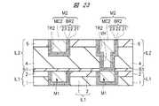
次に、図23に示されるように、配線溝TR2およびビアホールVHの外部の不要な主導体膜MC2およびバリア導体膜BR2(21,22,23)をCMP法による研磨処理などで除去し、配線溝TR2およびビアホールVH内に主導体膜MC2およびバリア導体膜BR2(21,22,23)を残すことにより、配線M2を形成する。この際の研磨処理を、以下では図23の研磨処理と称することとする。配線M2は、配線溝TR2内に埋め込まれた主導体膜MC2およびバリア導体膜BR2(21,22,23)からなる。図23の研磨処理を行うと、層間絶縁膜IL2の上面と配線M2の上面とが露出され、層間絶縁膜IL2の露出する上面と配線M2の露出する上面とは、ほぼ平坦な面を形成する。 Next, as shown in FIG. 23, unnecessary main conductor film MC2 and barrier conductor film BR2 (21, 22, 23) outside the wiring trench TR2 and the via hole VH are removed by a polishing process using a CMP method, etc. Wiring M2 is formed by leaving main conductor film MC2 and barrier conductor film BR2 (21, 22, 23) in trench TR2 and via hole VH. The polishing process at this time is hereinafter referred to as the polishing process of FIG. The wiring M2 includes a main conductor film MC2 and a barrier conductor film BR2 (21, 22, 23) embedded in the wiring trench TR2. 23, the upper surface of the interlayer insulating film IL2 and the upper surface of the wiring M2 are exposed, and the upper surface of the exposed interlayer insulating film IL2 and the exposed upper surface of the wiring M2 form a substantially flat surface. .
なお、ビアホールVH内に埋め込まれた主導体膜MC2およびバリア導体膜BR2により、配線M2のビア部が形成されている。ビアホールVH内に埋め込まれた配線M2のビア部は、配線溝TR2内に埋め込まれた配線M2と一体的に形成されている。このため、配線M2のビア部を、配線M2の一部とみなすこともできる。配線M2のビア部は、配線M1の上面に接してその配線M1に電気的に接続されている。このため、配線M2を配線M2のビア部を介して、配線M1と電気的に接続することができる。 The via portion of the wiring M2 is formed by the main conductor film MC2 and the barrier conductor film BR2 embedded in the via hole VH. The via portion of the wiring M2 embedded in the via hole VH is formed integrally with the wiring M2 embedded in the wiring trench TR2. For this reason, the via part of the wiring M2 can also be regarded as a part of the wiring M2. The via portion of the wiring M2 is in contact with the upper surface of the wiring M1 and is electrically connected to the wiring M1. Therefore, the wiring M2 can be electrically connected to the wiring M1 through the via portion of the wiring M2.
酸化シリコン膜6は、図23の研磨処理による研磨圧力またはスクラッチダメージなどから、酸化シリコン膜6よりも下の構造を保護するように機能することができる。酸化シリコン膜6は、図23の研磨処理で除去され得る。このため、図23の研磨処理を行うと、SiOC膜5の上面が露出され、SiOC膜5の上面と、配線M2の上面とは、ほぼ平坦な面を形成する。 The
また、図23の研磨処理で酸化シリコン膜6が除去されてSiOC膜5の上面が露出された場合を、図23に示しており、この場合は、図23の研磨処理を行った後は、層間絶縁膜IL2は、ポーラスLow−k膜4とポーラスLow−k膜4上のSiOC膜5との積層膜で構成されることになる。他の形態として、図23の研磨処理において、酸化シリコン膜6が層状に残存する場合もあり得る。その場合は、図23の研磨処理を行った後も、層間絶縁膜IL2は、ポーラスLow−k膜4とポーラスLow−k膜4上のSiOC膜5とSiOC膜5上の酸化シリコン膜6との積層膜で構成されることになる。 FIG. 23 shows a case where the
このようにして、配線M2を形成することができる。 In this way, the wiring M2 can be formed.
次に、必要に応じて、配線M2を埋め込んだ層間絶縁膜IL2の表面に対してアンモニアプラズマ処理などを施して、配線M2の上面および層間絶縁膜IL2の上面を清浄化する。 Next, if necessary, the surface of the interlayer insulating film IL2 in which the wiring M2 is embedded is subjected to ammonia plasma treatment or the like to clean the upper surface of the wiring M2 and the upper surface of the interlayer insulating film IL2.
次に、図24に示されるように、配線M2が埋め込まれた層間絶縁膜IL2上に、配線M2を覆うように、バリア絶縁膜B2を形成する。 Next, as illustrated in FIG. 24, a barrier insulating film B2 is formed on the interlayer insulating film IL2 in which the wiring M2 is embedded so as to cover the wiring M2.
バリア絶縁膜B2は、例えば、SiN膜、SiC膜、SiCN膜、およびSiCO膜から選択した一層以上により形成することができる。一例を挙げれば、バリア絶縁膜B2として、SiCN膜とその上のSiCO膜との積層膜を用いることができる。バリア絶縁膜B2は、CVD法などを用いて形成することができる。 The barrier insulating film B2 can be formed by, for example, one or more layers selected from a SiN film, a SiC film, a SiCN film, and a SiCO film. As an example, a laminated film of a SiCN film and a SiCO film thereon can be used as the barrier insulating film B2. The barrier insulating film B2 can be formed using a CVD method or the like.
その後、図12〜図24の工程と同様の工程を繰り返して、更に上層の配線層を形成することができるが、ここではその図示および繰り返しの説明は省略する。簡単に言えば、バリア絶縁膜B2上に層間絶縁膜IL2に相当する層間絶縁膜を形成し、バリア絶縁膜B2とその層間絶縁膜との積層膜に、配線溝TR2に相当する配線溝とビアホールVHに相当するビアホールを形成し、その配線溝およびビアホール内に、バリア導体膜BR2に相当するバリア導体膜と主導体膜MC2に相当する主導体膜とを埋め込むことにより、配線を形成する。その後、バリア絶縁膜B2に相当するバリア絶縁膜を形成する。これを、必要に応じて繰り返せばよい。 Thereafter, steps similar to those in FIGS. 12 to 24 can be repeated to form a further upper wiring layer, but the illustration and repeated description thereof are omitted here. In brief, an interlayer insulating film corresponding to the interlayer insulating film IL2 is formed on the barrier insulating film B2, and a wiring groove and a via hole corresponding to the wiring groove TR2 are formed in a laminated film of the barrier insulating film B2 and the interlayer insulating film. A via hole corresponding to VH is formed, and a wiring is formed by embedding a barrier conductor film corresponding to the barrier conductor film BR2 and a main conductor film corresponding to the main conductor film MC2 in the wiring groove and via hole. Thereafter, a barrier insulating film corresponding to the barrier insulating film B2 is formed. This may be repeated as necessary.
<本発明者の検討について>
本発明者は、層間絶縁膜に埋め込んだ銅配線(埋込銅配線)に関する技術について、特にバリア導体膜について検討している。<About the inventors'examination>
The inventor is examining a technique relating to a copper wiring (buried copper wiring) embedded in an interlayer insulating film, particularly a barrier conductor film.
図25は、本発明者が検討した第1検討例の半導体装置の要部断面図であり、上記図1に相当するものである。 FIG. 25 is a cross-sectional view of the principal part of the semiconductor device of the first study example studied by the present inventors, and corresponds to FIG.
図25の第1検討例の半導体装置が、上記図1の本実施の形態の半導体装置と相違しているのは、埋込銅配線の構成であり、特にバリア導体膜の構成である。バリア絶縁膜(B1,B2)と層間絶縁膜(IL1,IL2)とについては、図25の第1検討例の半導体装置と上記図1の本実施の形態の半導体装置とで共通である。 The semiconductor device of the first study example of FIG. 25 differs from the semiconductor device of the present embodiment of FIG. 1 in the configuration of the embedded copper wiring, particularly the configuration of the barrier conductor film. The barrier insulating films (B1, B2) and the interlayer insulating films (IL1, IL2) are common to the semiconductor device of the first study example in FIG. 25 and the semiconductor device of the present embodiment in FIG.
埋込銅配線は、バリア導体膜と、銅を主成分とする主導体膜とにより形成されている。上記図1の本実施の形態の場合は、バリア導体膜BR1と、銅を主成分とする主導体膜MC1とにより、埋込銅配線である配線M1が形成され、バリア導体膜BR2と、銅を主成分とする主導体膜MC2とにより、埋込銅配線である配線M2が形成されている。一方、図25の第1検討例の場合は、バリア導体膜BR101と、銅を主成分とする主導体膜MC101とにより、埋込銅配線である配線M101が形成され、バリア導体膜BR102と、銅を主成分とする主導体膜MC102とにより、埋込銅配線である配線M102が形成されている。 The embedded copper wiring is formed of a barrier conductor film and a main conductor film containing copper as a main component. In the case of the present embodiment shown in FIG. 1, the barrier conductor film BR1 and the main conductor film MC1 mainly composed of copper form a wiring M1 which is an embedded copper wiring, and the barrier conductor film BR2 and the copper conductor A wiring M2 which is a buried copper wiring is formed by the main conductor film MC2 whose main component is. On the other hand, in the case of the first study example of FIG. 25, the barrier conductor film BR101 and the main conductor film MC101 mainly composed of copper form a wiring M101 which is an embedded copper wiring, and the barrier conductor film BR102, A wiring M102 which is an embedded copper wiring is formed by the main conductor film MC102 mainly composed of copper.
配線M101は、本実施の形態の配線M1に相当するものであり、層間絶縁膜IL1に埋め込まれており、配線M102は、本実施の形態の配線M2に相当するものであり、層間絶縁膜IL2に埋め込まれている。 The wiring M101 corresponds to the wiring M1 of the present embodiment and is embedded in the interlayer insulating film IL1, and the wiring M102 corresponds to the wiring M2 of the present embodiment, and the interlayer insulating film IL2 Embedded in.
埋込銅配線を構成するバリア導体膜(BR1,BR2,BR101,BR102)は、銅の主導体膜(MC1,MC2,MC101,MC102)中の銅(Cu)が層間絶縁膜(IL1,IL2)中に拡散するのを抑制または防止する機能を有している。また、埋込銅配線を構成するバリア導体膜(BR1,BR2,BR101,BR102)は、埋込銅配線と層間絶縁膜(IL1,IL2)との密着性を向上させる機能も有している。 In the barrier conductor films (BR1, BR2, BR101, BR102) constituting the embedded copper wiring, the copper (Cu) in the copper main conductor films (MC1, MC2, MC101, MC102) is an interlayer insulating film (IL1, IL2). It has a function of suppressing or preventing diffusion into the inside. Further, the barrier conductor films (BR1, BR2, BR101, BR102) constituting the embedded copper wiring also have a function of improving the adhesion between the embedded copper wiring and the interlayer insulating films (IL1, IL2).
このため、埋込銅配線を構成するバリア導体膜としては、銅(Cu)に対するバリア性に優れた材料膜、すなわち、銅(Cu)の拡散を抑制または防止する機能が高い材料膜、を用いることが好ましい。また、埋込銅配線を構成するバリア導体膜としては、埋込銅配線と層間絶縁膜との間の密着性を向上させ得る材料膜を用いることが好ましい。このため、埋込銅配線を構成するバリア導体膜としては、タンタル膜や窒化タンタル膜が好適である。 For this reason, as the barrier conductor film constituting the embedded copper wiring, a material film having an excellent barrier property against copper (Cu), that is, a material film having a high function of suppressing or preventing the diffusion of copper (Cu) is used. It is preferable. Further, as the barrier conductor film constituting the embedded copper wiring, it is preferable to use a material film that can improve the adhesion between the embedded copper wiring and the interlayer insulating film. For this reason, a tantalum film or a tantalum nitride film is suitable as the barrier conductor film constituting the embedded copper wiring.
図25の第1検討例の場合は、配線M101のバリア導体膜BR101は、窒化タンタル(TaN)膜101と、窒化タンタル膜101上のタンタル(Ta)膜102との積層膜からなり、配線M102のバリア導体膜BR102は、窒化タンタル(TaN)膜103と、窒化タンタル膜103上のタンタル(Ta)膜104との積層膜からなる。 In the case of the first study example in FIG. 25, the barrier conductor film BR101 of the wiring M101 is composed of a laminated film of a tantalum nitride (TaN)
窒化タンタル膜とタンタル膜とは、いずれも銅(Cu)に対するバリア性に優れており、また、窒化タンタル膜は、層間絶縁膜との密着性に優れ、タンタル膜は、銅の主導体膜との密着性に優れている。このため、バリア導体膜として、窒化タンタル膜と該窒化タンタル膜上のタンタル膜との積層膜を用いることにより、埋込銅配線中の銅(Cu)が層間絶縁膜中に拡散するのを抑制または防止できるとともに、埋込銅配線と層間絶縁膜との密着性を向上させることができる。 Both the tantalum nitride film and the tantalum film have excellent barrier properties against copper (Cu), the tantalum nitride film has excellent adhesion to the interlayer insulating film, and the tantalum film has a copper main conductor film. Excellent adhesion. For this reason, by using a laminated film of a tantalum nitride film and a tantalum film on the tantalum nitride film as the barrier conductor film, it is possible to suppress diffusion of copper (Cu) in the embedded copper wiring into the interlayer insulating film. Alternatively, it can be prevented, and the adhesion between the buried copper wiring and the interlayer insulating film can be improved.
ここで、図25の第1検討例で用いている窒化タンタル膜101,103は、高密度な窒化タンタル膜、従って緻密な窒化タンタル膜からなる。なぜなら、窒化タンタル膜101,103の銅(Cu)のバリア性を高めるためには、窒化タンタル膜101,103を、高密度な窒化タンタル膜、従って緻密な窒化タンタル膜とした方が有利だからである。 Here, the
しかしながら、図25の第1検討例の場合は、次のような課題が発生することが、本発明者の検討により分かった。 However, in the case of the first study example in FIG. 25, it has been found by the inventor's study that the following problem occurs.
すなわち、窒化タンタル膜101,103が、高密度な窒化タンタル膜、従って緻密な窒化タンタル膜である場合は、窒化タンタル膜101,103を形成する際に、層間絶縁膜IL1,IL2にダメージが生じやすい。特に、窒化タンタル膜101,103をスパッタリング法により成膜する場合、成膜する窒化タンタル膜101,103の密度を高くしようとすると、成膜時にターゲットから飛来したスパッタ粒子が層間絶縁膜に衝突して与える衝撃も大きくなり、層間絶縁膜にダメージが生じやすくなる。 That is, when the
この窒化タンタル膜101,103を形成する際の層間絶縁膜のダメージは、その層間絶縁膜がポーラスLow−k膜を含んでいる場合に問題になる。なぜなら、ポーラスLow−k膜は、ポーラスであるがゆえに、誘電率を低くすることはできるが、機械的強度が弱く、窒化タンタル膜101,103を形成する際のダメージに対する耐性が低いからである。すなわち、ポーラスLow−k膜は、スパッタリング法によって窒化タンタル膜101,103を成膜する際に、ターゲットから飛来するスパッタ粒子による物理的な衝撃によってダメージを受けやすく、そのダメージによる影響が大きい。層間絶縁膜IL1,IL2に含まれるポーラスLow−k膜がダメージを受けてしまうと、半導体装置の信頼性が低下する虞がある。例えば、層間絶縁膜IL1,IL2に含まれるポーラスLow−k膜がダメージを受けてしまうと、そのポーラスLow−k膜が吸湿しやすくなる。ポーラスLow−k膜が吸湿してしまうと、バリア導体膜BR101,BR102の酸化が引き起こされ、配線M101,M102と層間絶縁膜IL1,IL2との間の密着性の低下や、配線M101,M102の信頼性(EM寿命、SM寿命あるいはTDDB寿命などの信頼性)の低下を招いてしまう。なお、配線の信頼性の評価として、EM(Electromigration:エレクトロマイグレーション)寿命、SM(Stressmigration:ストレスマイグレーション)、およびTDDB(Time Dependent Dielectric Breakdown)寿命などがある。また、ポーラスLow−k膜が吸湿してしまうと、層間絶縁膜IL1,IL2の誘電率が上昇してしまう懸念もある。これらは、半導体装置の信頼性が低下につながる。 The damage to the interlayer insulating film when forming the
それに対して、層間絶縁膜IL1,IL2にポーラスLow−k膜を使用しないことも考えられるが、ポーラスLow−k膜は、ポーラスではないLow−k膜に比べて誘電率を低下させやすいため、低誘電率絶縁膜として優れている。このため、層間絶縁膜IL1,IL2がポーラスLow−k膜を含むことで、配線間の寄生容量の低減効果を高めることができる。このため、本発明者は、層間絶縁膜がポーラスLow−k膜を含んでいても、埋込銅配線のバリア導体膜の成膜時にポーラスLow−k膜がダメージを受けないような構造について、検討した。 On the other hand, it is conceivable that the porous low-k film is not used for the interlayer insulating films IL1 and IL2, but the porous low-k film tends to lower the dielectric constant as compared with the low-k film that is not porous. Excellent as a low dielectric constant insulating film. For this reason, since the interlayer insulating films IL1 and IL2 include the porous Low-k film, the effect of reducing the parasitic capacitance between the wirings can be enhanced. For this reason, the inventor of the present invention has a structure in which the porous Low-k film is not damaged when the barrier conductor film of the buried copper wiring is formed even if the interlayer insulating film includes the porous Low-k film. investigated.
図26は、本発明者が検討した第2検討例の半導体装置の要部断面図であり、上記図1や図25に相当するものである。 FIG. 26 is a fragmentary cross-sectional view of the semiconductor device of the second study example studied by the present inventors, and corresponds to FIG. 1 and FIG. 25 described above.
図26の第2検討例の半導体装置が、図25の第1検討例の半導体装置と相違しているのは、高密度な窒化タンタル膜101の代わりに、低密度な窒化タンタル膜101aを用い、高密度な窒化タンタル膜103の代わりに、低密度な窒化タンタル膜103aを用いていることである。このため、図26の第2検討例の場合は、配線M101のバリア導体膜BR101は、低密度の窒化タンタル膜101aと、窒化タンタル膜101a上のタンタル膜102との積層膜からなり、配線M102のバリア導体膜BR102は、低密度の窒化タンタル膜103aと、窒化タンタル膜103a上のタンタル膜104との積層膜からなる。第2検討例の窒化タンタル膜101a,103aの密度は、第1検討例の窒化タンタル膜101,103の密度よりも低い。 The semiconductor device of the second study example of FIG. 26 is different from the semiconductor device of the first study example of FIG. 25 in that a low-density
図26の第2検討例の場合、窒化タンタル膜101a,103aが、低密度な窒化タンタル膜であるため、窒化タンタル膜101a,103aを形成する際に、層間絶縁膜IL1,IL2にダメージが生じにくい。すなわち、窒化タンタル膜101a,103aをスパッタリング法により成膜する際に、密度が低い窒化タンタル膜101a,103aを成膜するのであれば、成膜時にターゲットから飛来したスパッタ粒子が層間絶縁膜に衝突して与える衝撃を小さくできるため、層間絶縁膜にダメージが生じにくくなる。つまり、第1検討例のように高密度の窒化タンタル膜101,103をスパッタリング法で形成しようとすると、層間絶縁膜IL1,IL2に含まれるポーラスLow−k膜がダメージを受けてしまうが、第2検討例のように低密度の窒化タンタル膜101a,103aをスパッタリング法で形成するのであれば、層間絶縁膜IL1,IL2に含まれるポーラスLow−k膜がダメージを受けにくくなる。このため、図25の第1検討例の場合に比べて、図26の第2検討例の場合は、埋込銅配線のバリア導体膜の成膜時に層間絶縁膜IL1,IL2に含まれるポーラスLow−k膜がダメージを受けることに起因した信頼性の低下を抑制できる。 In the case of the second study example in FIG. 26, since the
しかしながら、図26の第2検討例の場合、次のような課題が発生してしまう。 However, in the case of the second study example in FIG. 26, the following problem occurs.
すなわち、窒化タンタル膜101aの密度が低いと、窒化タンタル膜101aとその上に形成したタンタル膜102との間の密着性(接着強度)が低くなってしまい、窒化タンタル膜101aとタンタル膜102との間が剥離しやすくなる。なぜなら、低密度の窒化タンタル膜101aの表面は、平坦性が低いために、窒化タンタル膜101aとその上に形成したタンタル膜102との間の密着性を確保しにくいからである。 That is, when the density of the
つまり、図25の第1検討例の場合は、窒化タンタル膜101は、密度が高いため、表面の平坦性が高く、窒化タンタル膜101とその上に形成したタンタル膜102との間の密着性を確保しやすい。それに比べると、図26の第2検討例の場合は、窒化タンタル膜101aは、密度が低いため、表面の平坦性が低く、窒化タンタル膜101aとその上に形成したタンタル膜102との間の密着性が低くなってしまう。同様に、図26の第2検討例の場合は、窒化タンタル膜103aは、密度が低いため、表面の平坦性が低く、窒化タンタル膜103aとその上に形成したタンタル膜104との間の密着性が低くなってしまう。 That is, in the case of the first study example in FIG. 25, the
窒化タンタル膜101aとタンタル膜102との間の密着性や、窒化タンタル膜103aとタンタル膜104との間の密着性が低くなることは、配線M101,M102の信頼性の低下につながり、ひいては、半導体装置の信頼性の低下につながってしまう。 Decreasing the adhesion between the
このため、図25の第1検討例の場合と図26の第2検討例の場合のいずれの場合も、埋込銅配線のバリア導体膜が原因で半導体装置の信頼性が低下してしまう。 For this reason, in both cases of the first study example of FIG. 25 and the second study example of FIG. 26, the reliability of the semiconductor device is lowered due to the barrier conductor film of the embedded copper wiring.
<主要な特徴と効果について>
本実施の形態の主要な特徴のうちの一つは、埋込銅配線(M1,M2)のバリア導体膜(BR1,BR2)が、第1バリア導体膜(11,21)と、第1バリア導体膜(11,21)上に形成された第2バリア導体膜(12,22)と、第2バリア導体膜(12,22)に形成された第3バリア導体膜(13,23)とを有していることである。第1バリア導体膜(11,21)は、層間絶縁膜(IL1,IL2)の配線溝(TR1,TR2)の底面および側壁上に形成されている。銅を主成分とする主導体膜(MC1,MC2)は、第3バリア導体膜(13,23)上に形成されている。そして、第1バリア導体膜(11,21)と第2バリア導体膜(12,22)とは、同じ導体材料からなり、第3バリア導体膜(13,23)は、第1バリア導体膜(11,21)および第2バリア導体膜(12,22)とは異なる導体材料からなり、第1バリア導体膜(11,21)の密度は、第2バリア導体膜(12,22)の密度よりも低い。<Main features and effects>
One of the main features of the present embodiment is that the barrier conductor films (BR1, BR2) of the embedded copper wirings (M1, M2), the first barrier conductor films (11, 21), and the first barrier A second barrier conductor film (12, 22) formed on the conductor film (11, 21) and a third barrier conductor film (13, 23) formed on the second barrier conductor film (12, 22). It is to have. The first barrier conductor films (11, 21) are formed on the bottom and side walls of the wiring grooves (TR1, TR2) of the interlayer insulating films (IL1, IL2). The main conductor films (MC1, MC2) mainly composed of copper are formed on the third barrier conductor films (13, 23). The first barrier conductor film (11, 21) and the second barrier conductor film (12, 22) are made of the same conductor material, and the third barrier conductor film (13, 23) is the first barrier conductor film ( 11, 21) and the second barrier conductor film (12, 22) are made of a different conductor material, and the density of the first barrier conductor film (11, 21) is higher than the density of the second barrier conductor film (12, 22). Is also low.
なお、配線M1については、バリア導体膜11とバリア導体膜12とバリア導体膜13とが、それぞれ第1バリア導体膜と第2バリア導体膜と第3バリア導体膜とに対応している。また、配線M2については、バリア導体膜21とバリア導体膜22とバリア導体膜23とが、それぞれ第1バリア導体膜と第2バリア導体膜と第3バリア導体膜とに対応している。 For the wiring M1, the
本実施の形態では、層間絶縁膜(IL1,IL2)の配線溝(TR1,TR2)の底面および側壁上に形成される第1バリア導体膜(11,21)の密度を低くしている。もしも、第1バリア導体膜(11,21)の密度を高くしようとすると、すなわち、第1バリア導体膜(11,21)を緻密な膜にしようとすると、上記図25の第1検討例を参照して説明したように、第1バリア導体膜(11,21)を形成する際に、層間絶縁膜(IL1,IL2)に含まれているポーラスLow−k膜(1,4)が、ダメージを受けてしまう。しかしながら、本実施の形態では、第1バリア導体膜(11,21)の密度を低くしているため、第1バリア導体膜(11,21)を形成する際に、層間絶縁膜(IL1,IL2)に含まれているポーラスLow−k膜(1,4)がダメージを受けてしまうのを、抑制または防止することができる。すなわち、本実施の形態では、第1バリア導体膜(11,21)の密度を低くすることにより、配線溝(TR1,TR2)から露出するポーラスLow−k膜(1,4)のダメージを抑制または防止しながら、第1バリア導体膜(11,21)を形成することができるようになる。これにより、半導体装置の信頼性を向上させることができる。 In the present embodiment, the density of the first barrier conductor films (11, 21) formed on the bottom and side walls of the wiring trenches (TR1, TR2) of the interlayer insulating films (IL1, IL2) is lowered. If the density of the first barrier conductor film (11, 21) is to be increased, that is, if the first barrier conductor film (11, 21) is to be a dense film, the first study example of FIG. As described above, the porous low-k films (1, 4) included in the interlayer insulating films (IL1, IL2) are damaged when the first barrier conductor films (11, 21) are formed. Will receive. However, in the present embodiment, since the density of the first barrier conductor films (11, 21) is lowered, the interlayer insulating films (IL1, IL2) are formed when the first barrier conductor films (11, 21) are formed. ) Contained in the porous Low-k film (1, 4) can be suppressed or prevented. In other words, in the present embodiment, by reducing the density of the first barrier conductor film (11, 21), damage to the porous Low-k film (1, 4) exposed from the wiring groove (TR1, TR2) is suppressed. Alternatively, the first barrier conductor film (11, 21) can be formed while preventing it. Thereby, the reliability of the semiconductor device can be improved.
例えば、ポーラスLow−k膜(1,4)がダメージを受けた場合には、そのポーラスLow−k膜が吸湿しやすくなり、ポーラスLow−k膜が吸湿してしまうと、バリア導体膜の酸化が引き起こされ、配線(M1,M2)と層間絶縁膜(IL1,IL2)との間の密着性の低下や、配線(M1,M2)の信頼性(EM寿命、SM寿命あるいはTDDB寿命などの信頼性)の低下を招いてしまう。それに対して、本実施の形態では、層間絶縁膜(IL1,IL2)に含まれているポーラスLow−k膜(1,4)がダメージを受けてしまうのを、抑制または防止することができるため、ポーラスLow−k膜(1,4)がダメージを受けた場合の不具合を改善または解消することができ、半導体装置の信頼性を向上させることができる。 For example, when the porous Low-k film (1, 4) is damaged, the porous Low-k film is likely to absorb moisture, and if the porous Low-k film absorbs moisture, the barrier conductor film is oxidized. Causes a decrease in adhesion between the wiring (M1, M2) and the interlayer insulating film (IL1, IL2), and the reliability of the wiring (M1, M2) (EM life, SM life, TDDB life, etc.) ). In contrast, in the present embodiment, it is possible to suppress or prevent the porous Low-k films (1, 4) included in the interlayer insulating films (IL1, IL2) from being damaged. In addition, it is possible to improve or eliminate problems when the porous low-k film (1, 4) is damaged, and to improve the reliability of the semiconductor device.
更に、本実施の形態では、第1バリア導体膜(11,21)上に、第1バリア導体膜(11,21)と同じ導体材料からなる第2バリア導体膜(12,22)を形成し、この第2バリア導体膜(12,22)の密度を第1バリア導体膜(11,21)の密度よりも高くしている。 Furthermore, in the present embodiment, the second barrier conductor film (12, 22) made of the same conductor material as the first barrier conductor film (11, 21) is formed on the first barrier conductor film (11, 21). The density of the second barrier conductor film (12, 22) is higher than the density of the first barrier conductor film (11, 21).
上記図26の第2検討例のように、低密度のバリア導体膜(窒化タンタル膜101a,103aに対応)上に、その低密度のバリア導体膜(101a,103a)とは異なる材料からなるバリア導体膜(タンタル膜102,104)を形成する場合には、それらのバリア導体膜の間の密着性(接着強度)が低くなり、剥離しやすくなってしまう。 As in the second study example of FIG. 26, a barrier made of a material different from the low-density barrier conductor film (101a, 103a) on the low-density barrier conductor film (corresponding to the
このため、本実施の形態とは異なり、低密度の第1バリア導体膜(11,21)上に第1バリア導体膜(11,21)とは異なる材料からなる導体膜を形成した場合には、その導体膜と低密度の第1バリア導体膜(11,21)との間の密着性(接着強度)が低くなり、剥離しやすくなってしまう。 Therefore, unlike this embodiment, when a conductor film made of a material different from that of the first barrier conductor film (11, 21) is formed on the low-density first barrier conductor film (11, 21). The adhesion (adhesive strength) between the conductor film and the low-density first barrier conductor film (11, 21) is lowered, and the film is easily peeled off.
しかしながら、本実施の形態では、低密度の第1バリア導体膜(11,21)上には、第1バリア導体膜(11,21)と同じ材料からなる第2バリア導体膜(12,22)を形成しているため、第1バリア導体膜(11,21)の密度が小さくとも、第2バリア導体膜(12,22)と第1バリア導体膜(11,21)との間の密着性(接着強度)を確保することができる。これは、2層の膜を積層する場合は、2層の膜の材料が異なる場合よりも、2層の膜の材料が同じ場合の方が、その2層の膜の密着性(接着強度)を確保しやすく、剥離が発生しにくくなるからである。2層の膜の材料が異なる場合は、その2層の膜の間で、結晶構造や格子定数の違いなどに起因して、歪による剥離が発生しやすくなるが、2層の膜の材料が同じ場合は、その2層の膜の間で、歪による剥離が発生しにくくなる。 However, in the present embodiment, the second barrier conductor film (12, 22) made of the same material as the first barrier conductor film (11, 21) is formed on the low-density first barrier conductor film (11, 21). Therefore, even if the density of the first barrier conductor film (11, 21) is small, the adhesion between the second barrier conductor film (12, 22) and the first barrier conductor film (11, 21) (Adhesive strength) can be ensured. This is because when two-layer films are stacked, the adhesion of the two-layer films (adhesive strength) is greater when the two-layer film materials are the same than when the two-layer film materials are different. This is because it is easy to ensure, and peeling is less likely to occur. When the materials of the two-layer films are different, peeling due to strain is likely to occur between the two-layer films due to differences in crystal structure and lattice constant. In the same case, peeling due to strain is less likely to occur between the two layers of films.
本実施の形態では、第1バリア導体膜(11,21)上には、第1バリア導体膜(11,21)と同じ材料からなる第2バリア導体膜(12,22)を形成しているため、第1バリア導体膜(11,21)が、密度が低いことで表面の平坦性が低くなっていても、第2バリア導体膜(12,22)と第1バリア導体膜(11,21)との間の密着性を確保することができる。従って、第2バリア導体膜(12,22)と第1バリア導体膜(11,21)との間の密着性(接着強度)を高めて、第2バリア導体膜(12,22)と第1バリア導体膜(11,21)との間の剥離を抑制または防止することができる。これにより、半導体装置の信頼性を向上させることができる。 In the present embodiment, the second barrier conductor film (12, 22) made of the same material as the first barrier conductor film (11, 21) is formed on the first barrier conductor film (11, 21). Therefore, even if the first barrier conductor film (11, 21) has low density and low surface flatness, the second barrier conductor film (12, 22) and the first barrier conductor film (11, 21) ) Can be secured. Therefore, the adhesiveness (adhesive strength) between the second barrier conductor film (12, 22) and the first barrier conductor film (11, 21) is increased, and the second barrier conductor film (12, 22) and the first barrier conductor film (12, 22) are improved. Separation between the barrier conductor films (11, 21) can be suppressed or prevented. Thereby, the reliability of the semiconductor device can be improved.
更に、本実施の形態では、第2バリア導体膜(12,22)上に、第2バリア導体膜(12,22)とは異なる導体材料からなる第3バリア導体膜(13,23)を形成している。 Further, in the present embodiment, the third barrier conductor film (13, 23) made of a conductor material different from the second barrier conductor film (12, 22) is formed on the second barrier conductor film (12, 22). doing.
第2バリア導体膜(12,22)と第3バリア導体膜(13,23)とは異なる導体材料からなるため、もしも第2バリア導体膜(12,22)の密度が低ければ、第2バリア導体膜(12,22)と第3バリア導体膜(13,23)との間の密着性が低くなり、第2バリア導体膜(12,22)と第3バリア導体膜(13,23)との間が剥離しやすくなる。 Since the second barrier conductor film (12, 22) and the third barrier conductor film (13, 23) are made of different conductor materials, if the density of the second barrier conductor film (12, 22) is low, the second barrier conductor film (12, 22) is formed. The adhesion between the conductor film (12, 22) and the third barrier conductor film (13, 23) is lowered, and the second barrier conductor film (12, 22) and the third barrier conductor film (13, 23) It becomes easy to peel between.
しかしながら、本実施の形態では、第2バリア導体膜(12,22)の密度を高くし、高密度の第2バリア導体膜(12,22)上に、第2バリア導体膜(12,22)とは異なる導体材料からなる第3バリア導体膜(13,23)を形成している。このため、第2バリア導体膜(12,22)と第3バリア導体膜(13,23)とが異なる導体材料から構成されていても、第2バリア導体膜(12,22)の密度を高くしていることで、第2バリア導体膜(12,22)の表面の平坦性が高くなっているため、第2バリア導体膜(12,22)と第3バリア導体膜(13,23)との間の密着性(接着強度)を確保することができる。すなわち、第2バリア導体膜(12,22)の密度が、第1バリア導体膜(11,21)の密度よりも高いことを反映して、第2バリア導体膜(12,22)の表面(第3バリア導体膜が形成される側の面)の平坦性は、第1バリア導体膜(11,21)の表面(第2バリア導体膜が形成される側の面)の平坦性よりも高くなり、第3バリア導体膜(13,23)の密着性を確保することができる。従って、第2バリア導体膜(12,22)と第3バリア導体膜(13,23)との間の密着性を高めて、第2バリア導体膜(12,22)と第3バリア導体膜(13,23)との間の剥離を抑制または防止することができる。これにより、半導体装置の信頼性を向上させることができる。 However, in the present embodiment, the density of the second barrier conductor film (12, 22) is increased, and the second barrier conductor film (12, 22) is formed on the high-density second barrier conductor film (12, 22). A third barrier conductor film (13, 23) made of a different conductor material is formed. For this reason, even if the second barrier conductor film (12, 22) and the third barrier conductor film (13, 23) are made of different conductor materials, the density of the second barrier conductor film (12, 22) is increased. By doing so, since the flatness of the surface of the second barrier conductor film (12, 22) is high, the second barrier conductor film (12, 22) and the third barrier conductor film (13, 23) Adhesiveness (adhesive strength) can be ensured. That is, reflecting the fact that the density of the second barrier conductor film (12, 22) is higher than the density of the first barrier conductor film (11, 21), the surface of the second barrier conductor film (12, 22) ( The flatness of the surface on the side where the third barrier conductor film is formed is higher than the flatness of the surface of the first barrier conductor film (11, 21) (the surface on the side where the second barrier conductor film is formed). Thus, the adhesion of the third barrier conductor film (13, 23) can be ensured. Therefore, the adhesion between the second barrier conductor film (12, 22) and the third barrier conductor film (13, 23) is enhanced, and the second barrier conductor film (12, 22) and the third barrier conductor film ( 13, 23) can be suppressed or prevented. Thereby, the reliability of the semiconductor device can be improved.
このように、本実施の形態では、層間絶縁膜(IL1,IL2)がポーラスLow−k膜(1,4)を含んでいるため、ポーラスLow−k膜(1,4)が露出した状態で形成する第1バリア導体膜(11,21)の密度を低くして、第1バリア導体膜(11,21)を形成する際のポーラスLow−k膜(1,4)のダメージを抑制または防止する。そして、低密度の第1バリア導体膜(11,21)上に、異種材料からなる導体膜を形成すると、その導体膜の密着性が低下してしまうことを考慮して、低密度の第1バリア導体膜(11,21)上には、第1バリア導体膜(11,21)と同じ材料からなる高密度の第2バリア導体膜(12,22)を形成する。そして、この高密度の第2バリア導体膜(12,22)上に、第2バリア導体膜(12,22)と異なる材料からなる第3バリア導体膜(13,23)を形成することにより、第2バリア導体膜(12,22)の密着性と、第3バリア導体膜(13,23)の密着性とを確保することができる。これにより、埋込銅配線(M1,M2)において、膜間の密着性が低くなる領域が生じるのを抑制または防止することができるようになるため、埋込銅配線(M1,M2)の信頼性を向上させることができる。従って、半導体装置の総合的な信頼性を向上させることができる。 Thus, in this embodiment, since the interlayer insulating films (IL1, IL2) include the porous Low-k film (1, 4), the porous Low-k film (1, 4) is exposed. The density of the first barrier conductor film (11, 21) to be formed is lowered to suppress or prevent damage to the porous Low-k film (1, 4) when the first barrier conductor film (11, 21) is formed. To do. Then, in consideration of the fact that when a conductive film made of a different material is formed on the low-density first barrier conductive film (11, 21), the adhesion of the conductive film is lowered, the low-density first A high-density second barrier conductor film (12, 22) made of the same material as the first barrier conductor film (11, 21) is formed on the barrier conductor film (11, 21). And on this high-density second barrier conductor film (12, 22), by forming a third barrier conductor film (13, 23) made of a material different from the second barrier conductor film (12, 22), The adhesion of the second barrier conductor film (12, 22) and the adhesion of the third barrier conductor film (13, 23) can be ensured. As a result, in the embedded copper wiring (M1, M2), it is possible to suppress or prevent the occurrence of a region in which the adhesion between the films is lowered. Therefore, the reliability of the embedded copper wiring (M1, M2) can be reduced. Can be improved. Therefore, the overall reliability of the semiconductor device can be improved.
このため、本実施の形態では、第1バリア導体膜(11,21)と第1バリア導体膜(11,21)上に形成する第2バリア導体膜(12,22)とを、同じ導体材料により形成するとともに、第1バリア導体膜(11,21)の密度を第2バリア導体膜(12,22)の密度よりも低くしている。これにより、第1バリア導体膜(11,21)の密度を低くし、第2バリア導体膜(12,22)の密度を高くすることができる。第1バリア導体膜(11,21)の密度を低くすることができるため、第1バリア導体膜(11,21)を形成する際に層間絶縁膜(IL1,IL2)に含まれるポーラスLow−k膜(1,4)がダメージを受けるのを抑制または防止することができる。そして、第2バリア導体膜(12,22)の密度を高くすることができるため、第2バリア導体膜(12,22)上に、第2バリア導体膜(12,22)とは異なる導体材料からなる第3バリア導体膜(13,23)を形成しても、第2バリア導体膜(12,22)の密着性と、第3バリア導体膜(13,23)の密着性とを確保することができる。これにより、層間絶縁膜(IL1,IL2)に含まれるポーラスLow−k膜(1,4)のダメージを抑制または防止することができるとともに、埋込銅配線(M1,M2)において、膜間の密着性が低くなる領域が生じるのを抑制または防止することができる。従って、半導体装置の総合的な信頼性を向上させることができる。 Therefore, in the present embodiment, the first barrier conductor film (11, 21) and the second barrier conductor film (12, 22) formed on the first barrier conductor film (11, 21) are made of the same conductor material. And the density of the first barrier conductor film (11, 21) is lower than the density of the second barrier conductor film (12, 22). Thereby, the density of the 1st barrier conductor film (11, 21) can be made low, and the density of the 2nd barrier conductor film (12, 22) can be made high. Since the density of the first barrier conductor films (11, 21) can be lowered, the porous Low-k included in the interlayer insulating films (IL1, IL2) when the first barrier conductor films (11, 21) are formed. It is possible to suppress or prevent the film (1, 4) from being damaged. Since the density of the second barrier conductor film (12, 22) can be increased, a conductor material different from the second barrier conductor film (12, 22) on the second barrier conductor film (12, 22). Even when the third barrier conductor film (13, 23) is formed, the adhesion of the second barrier conductor film (12, 22) and the adhesion of the third barrier conductor film (13, 23) are ensured. be able to. As a result, damage to the porous Low-k films (1, 4) included in the interlayer insulating films (IL1, IL2) can be suppressed or prevented, and in the embedded copper wirings (M1, M2) It is possible to suppress or prevent the occurrence of a region with low adhesion. Therefore, the overall reliability of the semiconductor device can be improved.
また、第2バリア導体膜(12,22)の膜厚は、第1バリア導体膜(11,21)の膜厚よりも大きいことが好ましい。言い換えると、第1バリア導体膜(11,21)の膜厚は、第2バリア導体膜(12,22)の膜厚よりも小さいことが好ましい。すなわち、配線M1において、バリア導体膜12の膜厚は、バリア導体膜11の膜厚よりも大きいことが好ましい。また、配線M2において、バリア導体膜22の膜厚は、バリア導体膜21の膜厚よりも大きいことが好ましい。その理由は、次のようなものである。 The film thickness of the second barrier conductor film (12, 22) is preferably larger than the film thickness of the first barrier conductor film (11, 21). In other words, the film thickness of the first barrier conductor film (11, 21) is preferably smaller than the film thickness of the second barrier conductor film (12, 22). That is, in the wiring M <b> 1, the film thickness of the
すなわち、第1バリア導体膜(11,21)と第2バリア導体膜(12,22)と第3バリア導体膜(13,23)とは、銅(Cu)に対するバリア性(バリア効果)を有しており、主導体膜(MC1,MC2)中の銅(Cu)が層間絶縁膜(IL1,IL2)中に拡散するのを抑制または防止するように機能することができる。第1バリア導体膜(11,21)の膜厚と第2バリア導体膜(12,22)の膜厚とが同じ場合は、低密度の第1バリア導体膜(11,21)よりも、高密度の第2バリア導体膜(12,22)の方が、銅(Cu)に対するバリア性は、高くなる。このため、第1バリア導体膜(11,21)の膜厚と第2バリア導体膜(12,22)の膜厚との合計を一定にした場合、第1バリア導体膜(11,21)の膜厚を増やすよりも、第2バリア導体膜(12,22)の膜厚を増やした方が、主導体膜(MC1,MC2)中の銅(Cu)が層間絶縁膜(IL1,IL2)中に拡散するのを抑制または防止する効果が大きくなる。また、第1バリア導体膜(11,21)の膜厚と第2バリア導体膜(12,22)の膜厚との合計を大きくすることは、配線(M1,M2)に占める主導体膜(MC1,MC2)の割合の低下につながり、配線(M1,M2)の抵抗の増加につながってしまう。 That is, the first barrier conductor film (11, 21), the second barrier conductor film (12, 22), and the third barrier conductor film (13, 23) have a barrier property (barrier effect) against copper (Cu). Thus, the copper (Cu) in the main conductor films (MC1, MC2) can function to suppress or prevent the copper (Cu) from diffusing into the interlayer insulating films (IL1, IL2). When the film thickness of the first barrier conductor film (11, 21) and the film thickness of the second barrier conductor film (12, 22) are the same, it is higher than the low-density first barrier conductor film (11, 21). The barrier property against copper (Cu) is higher in the second barrier conductor film (12, 22) having a higher density. Therefore, when the sum of the film thickness of the first barrier conductor film (11, 21) and the film thickness of the second barrier conductor film (12, 22) is constant, the first barrier conductor film (11, 21) Rather than increasing the film thickness, increasing the film thickness of the second barrier conductor film (12, 22) causes the copper (Cu) in the main conductor film (MC1, MC2) to be in the interlayer insulating film (IL1, IL2). The effect of suppressing or preventing diffusion to the surface increases. In addition, increasing the total thickness of the first barrier conductor film (11, 21) and the second barrier conductor film (12, 22) increases the main conductor film (M1, M2) This leads to a decrease in the ratio of MC1, MC2), leading to an increase in the resistance of the wiring (M1, M2).
このため、第1バリア導体膜(11,21)の膜厚を、第2バリア導体膜(12,22)の膜厚よりも小さくすることが好ましい。これにより、第1バリア導体膜(11,21)の膜厚と第2バリア導体膜(12,22)の膜厚との合計を増加させずに、バリア導体膜全体の銅(Cu)に対するバリア性を高めることができる。このため、主導体膜(MC1,MC2)中の銅(Cu)が層間絶縁膜(IL1,IL2)中に拡散するのを抑制または防止する効果を高めることができる。また、銅(Cu)に対するバリア性を確保しながら、第1バリア導体膜(11,21)の膜厚と第2バリア導体膜(12,22)の膜厚との合計を抑制することができるため、配線(M1,M2)の抵抗を低減することができる。 For this reason, it is preferable to make the film thickness of the first barrier conductor film (11, 21) smaller than the film thickness of the second barrier conductor film (12, 22). Thus, the barrier against the copper (Cu) of the entire barrier conductor film without increasing the total thickness of the first barrier conductor film (11, 21) and the thickness of the second barrier conductor film (12, 22). Can increase the sex. For this reason, the effect of suppressing or preventing the diffusion of copper (Cu) in the main conductor films (MC1, MC2) into the interlayer insulating films (IL1, IL2) can be enhanced. Moreover, the total of the film thickness of the 1st barrier conductor film (11,21) and the film thickness of the 2nd barrier conductor film (12,22) can be suppressed, ensuring the barrier property with respect to copper (Cu). Therefore, the resistance of the wirings (M1, M2) can be reduced.
また、第1バリア導体膜(11,21)の膜厚が小さすぎると、高密度の第2バリア導体膜(12,22)を成膜する際に、層間絶縁膜(IL1,IL2)に含まれるポーラスLow−k膜(1,4)にダメージが生じることが懸念される。このため、第1バリア導体膜(11,21)の膜厚は、1nm以上であることが好ましい。特に、配線溝(TR1,TR2)から露出するポーラスLow−k膜(1,4)上における第1バリア導体膜(11,21)の膜厚が、1nm以上であることが、好ましい。これにより、第1バリア導体膜(11,21)上に高密度の第2バリア導体膜(12,22)を成膜する際に、層間絶縁膜(IL1,IL2)に含まれるポーラスLow−k膜(1,4)にダメージが生じるのを、的確に抑制または防止することができる。 If the film thickness of the first barrier conductor film (11, 21) is too small, it is included in the interlayer insulating films (IL1, IL2) when the high-density second barrier conductor film (12, 22) is formed. There is a concern that the porous Low-k film (1, 4) is damaged. Therefore, the film thickness of the first barrier conductor film (11, 21) is preferably 1 nm or more. In particular, the film thickness of the first barrier conductor film (11, 21) on the porous Low-k film (1, 4) exposed from the wiring trench (TR1, TR2) is preferably 1 nm or more. Accordingly, when the high-density second barrier conductor films (12, 22) are formed on the first barrier conductor films (11, 21), the porous Low-k included in the interlayer insulating films (IL1, IL2). It is possible to accurately suppress or prevent the film (1, 4) from being damaged.
また、上述したように、バリア導体膜全体の銅(Cu)のバリア性を高めるためには、第1バリア導体膜(11,21)の膜厚を増やすよりも、第2バリア導体膜(12,22)の膜厚を増やした方が、有利である。このため、第1バリア導体膜(11,21)は、あまり厚くし過ぎないことが望ましい。従って、第1バリア導体膜(11,21)の膜厚は、1nm以上で2nm以下の範囲が、特に好適である。 In addition, as described above, in order to increase the copper (Cu) barrier property of the entire barrier conductor film, the second barrier conductor film (12) is used rather than increasing the film thickness of the first barrier conductor film (11, 21). 22), it is advantageous to increase the film thickness. For this reason, it is desirable that the first barrier conductor film (11, 21) is not too thick. Therefore, the thickness of the first barrier conductor film (11, 21) is particularly preferably in the range of 1 nm to 2 nm.
また、第1バリア導体膜(11,21)の膜厚と第2バリア導体膜(12,22)の膜厚との合計は、5nm以上が好ましい。これにより、バリア導体膜の銅(Cu)に対するバリア性を十分に確保することができる。また、層間絶縁膜(IL1,IL2)と配線(M1,M2)との間の密着性(接着強度)を向上させることができる。 The total thickness of the first barrier conductor film (11, 21) and the second barrier conductor film (12, 22) is preferably 5 nm or more. Thereby, the barrier property with respect to copper (Cu) of a barrier conductor film is fully securable. In addition, adhesion (adhesive strength) between the interlayer insulating films (IL1, IL2) and the wirings (M1, M2) can be improved.
また、第1バリア導体膜(11,21)の膜厚と第2バリア導体膜(12,22)の膜厚との合計を大きくしすぎると、その分、配線(M1,M2)に占める主導体膜(MC1,MC2)の割合が小さくなり、配線抵抗の増加を招いてしまう。このため、第1バリア導体膜(11,21)の膜厚と第2バリア導体膜(12,22)の膜厚との合計は、5〜15nmの範囲内に設定すれば、より好ましい。 Further, if the total thickness of the first barrier conductor film (11, 21) and the second barrier conductor film (12, 22) is excessively increased, the amount occupied in the wiring (M1, M2) is increased accordingly. The ratio of the body films (MC1, MC2) is reduced, leading to an increase in wiring resistance. For this reason, it is more preferable if the sum of the film thickness of the first barrier conductor film (11, 21) and the film thickness of the second barrier conductor film (12, 22) is set within a range of 5 to 15 nm.
また、第3バリア導体膜(13,23)の膜厚は、3〜10nmの範囲内に設定すれば、より好ましい。これにより、バリア導体膜の銅(Cu)に対するバリア性を確保するとともに、層間絶縁膜(IL1,IL2)と配線(M1,M2)との間の密着性を向上させることができる。また、配線抵抗の増加も抑制できる。 The film thickness of the third barrier conductor film (13, 23) is more preferably set within a range of 3 to 10 nm. Thereby, while ensuring the barrier property with respect to copper (Cu) of a barrier conductor film, the adhesiveness between an interlayer insulation film (IL1, IL2) and wiring (M1, M2) can be improved. In addition, an increase in wiring resistance can be suppressed.
また、第1バリア導体膜(11,21)と第2バリア導体膜(12,22)とは、同じ材料からなるが、結晶構造も同じであることが好ましい。すなわち、バリア導体膜11とバリア導体膜12とは、同じ材料からなるとともに、バリア導体膜11の結晶構造とバリア導体膜12の結晶構造とが同じであることが好ましい。また、バリア導体膜21とバリア導体膜22とは、同じ材料からなるとともに、バリア導体膜21の結晶構造とバリア導体膜22の結晶構造とが同じであることが好ましい。これは、2層の膜を積層する場合は、2層の膜の材料が異なる場合よりも、2層の膜の材料が同じ場合の方が、その2層の膜の密着性(接着強度)を確保しやすく、更に2層の膜の結晶構造も同じであれば、その2層の膜の密着性(接着強度)を更に確保しやすいからである。すなわち、2層の膜において、材料だけでなく結晶構造も同じ場合は、その2層の膜の間で、歪による剥離が更に発生しにくくなる。 The first barrier conductor film (11, 21) and the second barrier conductor film (12, 22) are made of the same material, but preferably have the same crystal structure. That is, the
すなわち、第1バリア導体膜(11,21)は、低密度であるため、表面の平坦性が低く、その上の形成する膜の密着性が低くなりやすい。しかしながら、第1バリア導体膜(11,21)上に形成する第2バリア導体膜(12,22)が、第1バリア導体膜(11,21)と材料が同じで結晶構造も同じであれば、第1バリア導体膜(11,21)が、低密度で表面の平坦性が低くとも、第2バリア導体膜(12,22)の密着性を高めることができる。これにより、第1バリア導体膜(11,21)と第2バリア導体膜(12,22)との間で剥離が生じるのを、より的確に抑制または防止することができる。 That is, since the first barrier conductor film (11, 21) has a low density, the surface flatness is low, and the adhesion of the film formed thereon tends to be low. However, if the second barrier conductor film (12, 22) formed on the first barrier conductor film (11, 21) is the same material and the same crystal structure as the first barrier conductor film (11, 21) Even if the first barrier conductor film (11, 21) has low density and low surface flatness, the adhesion of the second barrier conductor film (12, 22) can be enhanced. Thereby, it is possible to more accurately suppress or prevent the separation between the first barrier conductor film (11, 21) and the second barrier conductor film (12, 22).
また、本実施の形態では、第1バリア導体膜(11,21)と第2バリア導体膜(12,22)とは、いずれも窒化タンタル膜からなることが好ましい。なぜなら、窒化タンタル膜は、銅(Cu)に対するバリア性に優れているとともに、層間絶縁膜(IL1,IL2)に対する密着性にも優れているからである。すなわち、窒化タンタル膜とタンタル膜とを比べると、窒化タンタル膜の方が、層間絶縁膜(IL1,IL2)に対する密着性に、より優れている。このため、層間絶縁膜(IL1,IL2)に接する第1バリア導体膜(11,21)として、窒化タンタル膜を用いることにより、銅(Cu)に対するバリア性を確保するとともに、層間絶縁膜(IL1,IL2)に対する第1バリア導体膜(11,21)の密着性を高めることができる。これにより、第1バリア導体膜(11,21)と層間絶縁膜(IL1,IL2)との間で剥離が生じるのを、より的確に抑制または防止することができる。また、第2バリア導体膜(12,22)は、第1バリア導体膜(11,21)と同じ材料からなるため、第1バリア導体膜(11,21)が窒化タンタル膜であれば、第2バリア導体膜(12,22)も必然的に窒化タンタル膜となる。 In the present embodiment, it is preferable that both the first barrier conductor film (11, 21) and the second barrier conductor film (12, 22) are made of a tantalum nitride film. This is because the tantalum nitride film has excellent barrier properties against copper (Cu) and also has excellent adhesion to interlayer insulating films (IL1, IL2). That is, when the tantalum nitride film and the tantalum film are compared, the tantalum nitride film has better adhesion to the interlayer insulating films (IL1, IL2). Therefore, by using a tantalum nitride film as the first barrier conductor film (11, 21) in contact with the interlayer insulating film (IL1, IL2), the barrier property against copper (Cu) is secured and the interlayer insulating film (IL1 , IL2), the adhesion of the first barrier conductor film (11, 21) can be improved. Thereby, it is possible to more accurately suppress or prevent the occurrence of peeling between the first barrier conductor film (11, 21) and the interlayer insulating film (IL1, IL2). In addition, since the second barrier conductor film (12, 22) is made of the same material as the first barrier conductor film (11, 21), if the first barrier conductor film (11, 21) is a tantalum nitride film, The two barrier conductor films (12, 22) are necessarily tantalum nitride films.
また、本実施の形態では、第3バリア導体膜(13,23)は、タンタル膜からなることが好ましい。なぜなら、タンタル膜は、銅(Cu)に対するバリア性に優れているとともに、銅を主成分とする主導体膜(MC1,MC2)に対する密着性にも優れているからである。すなわち、窒化タンタル膜とタンタル膜とを比べると、タンタル膜の方が、銅を主成分とする主導体膜(MC1,MC2)に対する密着性に、より優れている。このため、銅を主成分とする主導体膜(MC1,MC2)に接する第3バリア導体膜(13,23)として、タンタル膜を用いることにより、銅(Cu)に対するバリア性を確保するとともに、第3バリア導体膜(13,23)に対する主導体膜(MC1,MC2)の密着性を高めることができる。これにより、第3バリア導体膜(13,23)と主導体膜(MC1,MC2)との間で剥離が生じるのを、より的確に抑制または防止することができる。 In the present embodiment, the third barrier conductor film (13, 23) is preferably made of a tantalum film. This is because the tantalum film has excellent barrier properties against copper (Cu) and also has excellent adhesion to main conductor films (MC1 and MC2) mainly composed of copper. That is, when the tantalum nitride film and the tantalum film are compared, the tantalum film has better adhesion to the main conductor films (MC1 and MC2) mainly composed of copper. Therefore, by using a tantalum film as the third barrier conductor film (13, 23) in contact with the main conductor film (MC1, MC2) mainly composed of copper, the barrier property against copper (Cu) is secured, The adhesion of the main conductor films (MC1, MC2) to the third barrier conductor films (13, 23) can be improved. Thereby, it is possible to more accurately suppress or prevent the separation between the third barrier conductor film (13, 23) and the main conductor film (MC1, MC2).
従って、層間絶縁膜(IL1,IL2)に対する密着性がタンタル膜よりも優れている窒化タンタル膜を、第1バリア導体膜(11,21)および第2バリア導体膜(12,22)として用いることにより、層間絶縁膜(IL1,IL2)とバリア導体膜(BR1,BR2)との間の密着性を、より向上させることができる。そして、主導体膜(MC1,MC2)に対する密着性が窒化タンタル膜よりも優れているタンタル膜を、第3バリア導体膜(13,23)として用いることにより、主導体膜(MC1,MC2)とバリア導体膜(BR1,BR2)との間の密着性を、より向上させることができる。これにより、層間絶縁膜(IL1,IL2)とバリア導体膜(BR1,BR2)との間の密着性と、主導体膜(MC1,MC2)とバリア導体膜(BR1,BR2)との間の密着性との両方を、的確に向上させることができる。 Accordingly, a tantalum nitride film having better adhesion to the interlayer insulating films (IL1, IL2) than the tantalum film is used as the first barrier conductor film (11, 21) and the second barrier conductor film (12, 22). Thus, the adhesion between the interlayer insulating film (IL1, IL2) and the barrier conductor film (BR1, BR2) can be further improved. Then, by using a tantalum film having better adhesion to the main conductor films (MC1, MC2) than the tantalum nitride film as the third barrier conductor film (13, 23), the main conductor films (MC1, MC2) and The adhesion between the barrier conductor films (BR1, BR2) can be further improved. Thereby, the adhesion between the interlayer insulating film (IL1, IL2) and the barrier conductor film (BR1, BR2), and the adhesion between the main conductor film (MC1, MC2) and the barrier conductor film (BR1, BR2). Both can be improved accurately.
このように、第1バリア導体膜(11,21)および第2バリア導体膜(12,22)としては、窒化タンタル膜が最も好ましく、第3バリア導体膜(13,23)としては、タンタル膜が最も好ましい。それ以外には、第1バリア導体膜(11,21)および第2バリア導体膜(12,22)としては、窒化チタン(TiN)膜または窒化ルテニウム(RuN)膜を用いることもできる。また、第3バリア導体膜(13,23)としては、チタン(Ti)膜、タングステン(W)膜、コバルト(Co)膜、マンガン(Mn)膜またはルテニウム(Ru)膜、あるいは、これらの元素(Ti,W,Co,Mn,Ru)を2種類以上含む合金膜を用いることもできる。 As described above, the first barrier conductor film (11, 21) and the second barrier conductor film (12, 22) are most preferably a tantalum nitride film, and the third barrier conductor film (13, 23) is a tantalum film. Is most preferred. In addition, a titanium nitride (TiN) film or a ruthenium nitride (RuN) film can also be used as the first barrier conductor film (11, 21) and the second barrier conductor film (12, 22). As the third barrier conductor film (13, 23), a titanium (Ti) film, a tungsten (W) film, a cobalt (Co) film, a manganese (Mn) film, a ruthenium (Ru) film, or these elements An alloy film containing two or more types of (Ti, W, Co, Mn, Ru) can also be used.
また、本実施の形態では、第1バリア導体膜(11,21)の密度を、第2バリア導体膜(12,22)の密度よりも低くしているが、第1バリア導体膜(11,21)の密度は、完全結晶の密度の50〜90%であることが好ましい。すなわち、第1バリア導体膜(11,21)の密度は、第1バリア導体膜(11,21)を構成する材料の完全結晶の密度の50〜90%であることが好ましい。つまり、第1バリア導体膜(11,21)の密度をD1とし、第1バリア導体膜(11,21)を構成する材料の完全結晶の密度をD2としたときに、次の(式1)、
0.5≦D1/D2≦0.9 ・・・(式1)
が成り立つことが好ましい。なお、完全結晶とは、結晶欠陥や不純物が存在しない完全な結晶のことである。In the present embodiment, the density of the first barrier conductor film (11, 21) is lower than the density of the second barrier conductor film (12, 22). The density of 21) is preferably 50 to 90% of the density of the complete crystal. That is, the density of the first barrier conductor film (11, 21) is preferably 50 to 90% of the density of the complete crystal of the material constituting the first barrier conductor film (11, 21). In other words, the density of the first barrier conductor film (11, 21) andD 1, the density of perfect crystal of the material constituting the first barrier conductor film (11, 21) when theD 2, the following (formula 1),
0.5 ≦ D1 / D2 ≦ 0.9 (Formula 1)
Is preferably satisfied. Note that a complete crystal is a complete crystal free from crystal defects and impurities.
また、第2バリア導体膜(12,22)の密度は、完全結晶の密度の90%よりも大きいことが好ましい。すなわち、第2バリア導体膜(12,22)の密度は、第2バリア導体膜(12,22)を構成する材料の完全結晶の密度の90%よりも大きいことが好ましい。つまり、第2バリア導体膜(12,22)の密度をD3とし、第2バリア導体膜(12,22)を構成する材料の完全結晶の密度をD4としたときに、次の(式2)、
0.9<D3/D4≦1 ・・・(式2)
が成り立つことが好ましい。Further, the density of the second barrier conductor film (12, 22) is preferably larger than 90% of the density of the complete crystal. That is, the density of the second barrier conductor film (12, 22) is preferably greater than 90% of the density of the complete crystal of the material constituting the second barrier conductor film (12, 22). In other words, the density of the second barrier conductor film (12, 22) andD 3, the density of perfect crystal of the material constituting the second barrier conductor film (12, 22) when theD 4, the following (formula 2),
0.9 <D3 / D4 ≦ 1 (Formula 2)
Is preferably satisfied.
なお、第1バリア導体膜(11,21)を構成する材料と、第2バリア導体膜(12,22)を構成する材料とは、同じであるため、第1バリア導体膜(11,21)を構成する材料の完全結晶の密度(D2)と、第2バリア導体膜(12,22)を構成する材料の完全結晶の密度(D4)とは、同じであり、D2=D4が成り立つ。In addition, since the material which comprises the 1st barrier conductor film (11,21) and the material which comprises the 2nd barrier conductor film (12,22) are the same, the 1st barrier conductor film (11,21) The density (D2 ) of the perfect crystal of the material constituting the material and the density (D4 ) of the perfect crystal of the material constituting the second barrier conductor film (12, 22) are the same, and D2 = D4 Holds.
密度D2は、第1バリア導体膜(11,21)が完全結晶で構成されていると仮定したときの、その第1バリア導体膜(11,21)の仮想的な密度とみなすこともできる。また、密度D4は、第2バリア導体膜(12,22)が完全結晶で構成されていると仮定したときの、その第2バリア導体膜(12,22)の仮想的な密度とみなすこともできる。Density D2 can also be regarded as a virtual density of assuming that the first barrier conductor film (11, 21) is composed of perfect crystal, the first barrier conductor film (11, 21) . Further, the density D4 is regarded as a virtual density of the second barrier conductor film (12, 22) when it is assumed that the second barrier conductor film (12, 22) is composed of a complete crystal. You can also.
また、第1バリア導体膜(11,21)と第2バリア導体膜(12,22)とは、同じ材料からなるため、第1バリア導体膜(11,21)の密度が第2バリア導体膜(12,22)の密度よりも小さいことは、第1バリア導体膜(11,21)の原子空孔の濃度(空孔濃度)が第2バリア導体膜(12,22)の原子空孔の濃度(空孔濃度)よりも大きいことに対応している。従って、バリア導体膜11の原子空孔の濃度は、バリア導体膜12の原子空孔の濃度よりも大きく、また、バリア導体膜21の原子空孔の濃度は、バリア導体膜22の原子空孔の濃度よりも大きい。 Further, since the first barrier conductor film (11, 21) and the second barrier conductor film (12, 22) are made of the same material, the density of the first barrier conductor film (11, 21) is the second barrier conductor film. The density lower than the density of (12, 22) means that the atomic vacancy concentration (vacancy concentration) of the first barrier conductor film (11, 21) is smaller than that of the second barrier conductor film (12, 22). This corresponds to a concentration larger than the concentration (vacancy concentration). Therefore, the concentration of atomic vacancies in the
ここで、原子空孔の濃度とは、原子の占め得る全格子点に対する原子空孔の割合に対応している。また、原子空孔とは、原子が存在すべき結晶の格子点なのに、原子が存在していない箇所(格子点)に対応している。例えば、ある膜において、平均して10個の格子点毎に1つの原子空孔が存在している場合は、その膜の原子空孔の濃度は10%となり、その膜の密度は完全結晶の密度の90%となる。完全結晶は、原子空孔が存在しないため、完全結晶の原子空孔の濃度はゼロ%である。 Here, the concentration of atomic vacancies corresponds to the ratio of atomic vacancies to all lattice points that can be occupied by atoms. An atomic vacancy corresponds to a point (lattice point) where an atom does not exist although it is a lattice point of a crystal where an atom should exist. For example, in a certain film, when one atomic vacancy exists for every 10 lattice points on average, the concentration of atomic vacancies in the film is 10%, and the density of the film is completely crystalline. 90% of the density. Since the complete crystal has no atomic vacancies, the concentration of vacancies in the complete crystal is zero%.
従って、第1バリア導体膜(11,21)の原子空孔の濃度をD5とすると、次の(式3)、
D5=1−D1/D2 ・・・(式3)
が成り立つ。また、第2バリア導体膜(12,22)の原子空孔の濃度をD6とすると、次の(式4)、
D6=1−D3/D4 ・・・(式4)
が成り立つ。Therefore, when the concentration of atomic vacancies in the first barrier conductor film (11, 21) andD 5, the following equation (3),
D5 = 1−D1 / D2 (Formula 3)
Holds. Further, when the concentration of atomic vacancies in the second barrier conductor film (12, 22) andD 6, the following equation (4),
D6 = 1−D3 / D4 (Formula 4)
Holds.
このため、上述のように第1バリア導体膜(11,21)の密度(D1)は、完全結晶の密度(D2)の50〜90%であることが好ましいが、これは、第1バリア導体膜(11,21)の原子空孔の濃度(D5)は10〜50%であることが好ましいことに対応している。また、上述のように第2バリア導体膜(12,22)の密度(D3)は、完全結晶の密度(D4)の90%よりも大きいことが好ましいが、これは、第2バリア導体膜(12,22)の原子空孔の濃度(D6)は10%未満であることが好ましいことに対応している。Therefore, as described above, the density (D1 ) of the first barrier conductor film (11, 21) is preferably 50 to 90% of the density (D2 ) of the complete crystal. This corresponds to the fact that the atomic vacancy concentration (D5 ) of the barrier conductor film (11, 21) is preferably 10 to 50%. Further, as described above, the density (D3 ) of the second barrier conductor film (12, 22) is preferably larger than 90% of the density (D4 ) of the complete crystal. This corresponds to the fact that the atomic vacancy concentration (D6 ) of the film (12, 22) is preferably less than 10%.
ここで、窒化タンタルの結晶構造は、六方晶であり、その格子定数は、3.363オングストロームである。本実施の形態では、第1バリア導体膜(11,21)と第2バリア導体膜(12,22)とは、いずれも窒化タンタル膜であることが好ましい。その場合、第1バリア導体膜を構成する窒化タンタル膜と、第2バリア導体膜を構成する窒化タンタル膜とは、いずれも六方晶の結晶構造を有しているが、密度は、第2バリア導体膜よりも第1バリア導体膜の方が小さく、従って、原子空孔の濃度は、第2バリア導体膜よりも第1バリア導体膜の方が大きくなっている。なお、完全結晶の窒化タンタル(TaN)の密度(D2)は、14.3g/cm3である。なお、窒化タンタル膜がTa2Nの場合には、結晶構造が六方晶で格子定数が3.363オングストロームだと、完全結晶の密度は12.6g/cm3程度である。Here, the crystal structure of tantalum nitride is hexagonal, and its lattice constant is 3.363 angstroms. In the present embodiment, both the first barrier conductor films (11, 21) and the second barrier conductor films (12, 22) are preferably tantalum nitride films. In that case, the tantalum nitride film constituting the first barrier conductor film and the tantalum nitride film constituting the second barrier conductor film both have a hexagonal crystal structure, but the density is the second barrier film. The first barrier conductor film is smaller than the conductor film. Therefore, the concentration of atomic vacancies is higher in the first barrier conductor film than in the second barrier conductor film. The density (D2 ) of completely crystalline tantalum nitride (TaN) is 14.3 g / cm3 . When the tantalum nitride film is Ta2 N, the density of the complete crystal is about 12.6 g / cm3 when the crystal structure is hexagonal and the lattice constant is 3.363 Å.
なお、第1バリア導体膜(11,21)は、2原子層以上の原子層により形成することが好ましく、また、原子空孔の濃度を10〜50%とすることが好ましい。これにより、配線溝(TR1,TR2)の内面において、層間絶縁膜(IL1,IL2)が第1バリア導体膜(11,21)で完全に覆われるようになるとともに、第2バリア導体膜(12,22)と層間絶縁膜(IL1,IL2)との間の第1バリア導体膜(11,21)において、いずれの平面位置でも原子空孔がほぼ存在するようになる。これにより、バリア導体膜の形成に伴うポーラスLow−k膜(1,4)のダメージを抑制または防止できるという効果を、効果的に得ることができるようになる。この観点でも、上述のように、第1バリア導体膜(11,21)の膜厚は、1nm以上が好ましい。 The first barrier conductor film (11, 21) is preferably formed of two or more atomic layers, and the atomic vacancy concentration is preferably 10 to 50%. As a result, the interlayer insulating films (IL1, IL2) are completely covered with the first barrier conductor films (11, 21) on the inner surfaces of the wiring trenches (TR1, TR2), and the second barrier conductor film (12 , 22) and the first barrier conductor film (11, 21) between the interlayer insulating films (IL1, IL2), atomic vacancies almost exist at any plane position. Thereby, the effect that the damage of the porous Low-k film | membrane (1, 4) accompanying formation of a barrier conductor film can be suppressed or prevented can be acquired effectively. Also from this viewpoint, as described above, the film thickness of the first barrier conductor film (11, 21) is preferably 1 nm or more.
また、第1バリア導体膜(11,21)と第2バリア導体膜(12,22)とは、同じ材料からなり、かつ密度が相違している。製造された半導体装置においては、例えば、TEM(Transmission Electron Microscope:透過型電子顕微鏡)観察によるコントラストで、第1バリア導体膜(11,21)と第2バリア導体膜(12,22)との密度の違いを判別することができる。例えば、HAADF(High-angle annular dark field:高角度散乱暗視野)−STEM(scanning transmission electron microscope:走査透過電子顕微鏡)像では、原子量に比例したコントラストを取得できる。このため、HAADF−STEM像などを利用して、第1バリア導体膜(11,21)の密度が、第2バリア導体膜(12,22)の密度よりも低いことを判別することができる。 Further, the first barrier conductor film (11, 21) and the second barrier conductor film (12, 22) are made of the same material and have different densities. In the manufactured semiconductor device, for example, the density of the first barrier conductor film (11, 21) and the second barrier conductor film (12, 22) with contrast by observation with a TEM (Transmission Electron Microscope). Can be discriminated. For example, in a HAADF (High-angle annular dark field) -STEM (scanning transmission electron microscope) image, a contrast proportional to the atomic weight can be acquired. Therefore, it is possible to determine that the density of the first barrier conductor film (11, 21) is lower than the density of the second barrier conductor film (12, 22) using a HAADF-STEM image or the like.
また、第3バリア導体膜(13,23)の密度も、高いことが好ましく、これにより、第3バリア導体膜(13,23)と主導体膜(MC1,MC2)との間の密着性(接着強度)を向上させることができる。第3バリア導体膜(13,23)は、第2バリア導体膜(12,22)上に形成されるため、第3バリア導体膜(13,23)の密度が高くとも、第3バリア導体膜(13,23)の成膜時に層間絶縁膜(IL1,IL2)に含まれるポーラスLow−k膜(1,4)はダメージを受けずに済む。 The density of the third barrier conductor film (13, 23) is also preferably high, whereby the adhesion between the third barrier conductor film (13, 23) and the main conductor film (MC1, MC2) ( Adhesive strength) can be improved. Since the third barrier conductor film (13, 23) is formed on the second barrier conductor film (12, 22), the third barrier conductor film is formed even if the density of the third barrier conductor film (13, 23) is high. The porous Low-k films (1, 4) included in the interlayer insulating films (IL1, IL2) are not damaged during the deposition of (13, 23).
このため、第3バリア導体膜(13,23)の密度は、完全結晶の密度の90%よりも大きいことが好ましい。すなわち、第3バリア導体膜(13,23)の密度は、第3バリア導体膜(13,23)を構成する材料の完全結晶の密度の90%よりも大きいことが好ましい。つまり、第3バリア導体膜(13,23)の密度をD7とし、第3バリア導体膜(13,23)を構成する材料の完全結晶の密度をD8としたときに、次の(式5)、
0.9<D7/D8≦1 ・・・(式5)
が成り立つことが好ましい。For this reason, the density of the third barrier conductor film (13, 23) is preferably larger than 90% of the density of the complete crystal. That is, the density of the third barrier conductor film (13, 23) is preferably larger than 90% of the density of the complete crystal of the material constituting the third barrier conductor film (13, 23). In other words, the density of the third barrier conductor film (13, 23) andD 7, the density of perfect crystal of the material constituting the third barrier conductor film (13, 23) when theD 8, the following (formula 5),
0.9 <D7 / D8 ≦ 1 (Formula 5)
Is preferably satisfied.
密度D8は、第3バリア導体膜(13,23)が完全結晶で構成されていると仮定したときの、その第3バリア導体膜(13,23)の仮想的な密度とみなすこともできる。Density D8 is, assuming that the third barrier conductor film (13, 23) is composed of perfect crystal, may be regarded as a virtual density of the third barrier conductor film (13, 23) .
また、第3バリア導体膜(13,23)の原子空孔の濃度をD9とすると、次の(式6)、
D9=1−D7/D8 ・・・(式6)
が成り立つ。Further, when the concentration of atomic vacancies in the third barrier conductor film (13, 23) andD 9, the following equation (6),
D9 = 1−D7 / D8 (Formula 6)
Holds.
このため、上述のように第3バリア導体膜(13,23)の密度(D7)は、完全結晶の密度(D8)の90%よりも大きいことが好ましいが、これは、第3バリア導体膜(13,23)の原子空孔の濃度(D9)は10%未満であることが好ましいことに対応している。For this reason, as described above, the density (D7 ) of the third barrier conductor film (13, 23) is preferably larger than 90% of the density (D8 ) of the perfect crystal. This corresponds to the fact that the concentration (D9 ) of atomic vacancies in the conductor films (13, 23) is preferably less than 10%.
従って、第1バリア導体膜(11,21)の密度(D1)と、第2バリア導体膜(12,22)の密度(D3)と、第3バリア導体膜(13,23)の密度(D7)とで、次の(式7)、
D1/D2<D3/D4、かつ、D1/D2<D7/D8 ・・・(式7)
が成り立つことが望ましい。Therefore, the density of the first barrier conductor film (11 and 21)(D 1), the density of the second barrier conductor film (12, 22) and(D 3), the density of the third barrier conductor film (13, 23) (D7 ) and the following (Equation 7),
D 1 / D 2 <D 3 / D 4and,, D 1 / D 2 < D 7 / D 8 ··· ( Equation 7)
It is desirable that
この(式7)を原子空孔の濃度の観点で置き換えると、第2バリア導体膜(12,22)の原子空孔の濃度(D6)は、第1バリア導体膜(11,21)の原子空孔の濃度(D5)よりも大きく(D6>D5)、かつ、第3バリア導体膜(13,23)の原子空孔の濃度(D9)は、第1バリア導体膜(11,21)の原子空孔の濃度(D5)よりも大きい(D9>D5)ことが望ましい。When this (Equation 7) is replaced in terms of the concentration of atomic vacancies, the concentration (D6 ) of atomic vacancies in the second barrier conductor film (12, 22) is the same as that of the first barrier conductor film (11, 21). The concentration of the atomic vacancies (D9 ) in the third barrier conductor film (13, 23) is larger than the concentration of atomic vacancies (D5 ) (D6 > D5 ), and the first barrier conductor film ( It is desirable that (D9 > D5 ) be larger than the concentration of atomic vacancies (D5 ) of (11, 21).
なお、第1バリア導体膜(11,21)と第2バリア導体膜(12,22)とは同じ材料からなるが、第3バリア導体膜(13,23)は、第1バリア導体膜(11,21)および第2バリア導体膜(12,22)とは異なる材料からなる。このため、D2とD4とは同じ値(D2=D4)であるが、D8は、D2およびD4とは相違した値である。The first barrier conductor film (11, 21) and the second barrier conductor film (12, 22) are made of the same material, but the third barrier conductor film (13, 23) is the first barrier conductor film (11 , 21) and the second barrier conductor film (12, 22). Therefore, D2 and D4 are the same value (D2 = D4 ), but D8 is a value different from D2 and D4 .
ここで、タンタルの結晶構造は、体心立方構造であり、その格子定数は、3.305オングストロームである。本実施の形態では、第3バリア導体膜(13,23)は、タンタル膜であることが好ましく、その場合、第3バリア導体膜(13,23)を構成するタンタル膜は、体心立方構造の結晶構造を有している。なお、完全結晶のタンタルの密度(D8)は、16.65g/cm3である。Here, the crystal structure of tantalum is a body-centered cubic structure, and its lattice constant is 3.305 angstroms. In the present embodiment, the third barrier conductor film (13, 23) is preferably a tantalum film. In this case, the tantalum film constituting the third barrier conductor film (13, 23) has a body-centered cubic structure. It has a crystal structure of Note that the density of tantalum (D8 ) in the complete crystal is 16.65 g / cm3 .
また、後述の実施の形態2では、第1バリア導体膜(11,21)と第2バリア導体膜(12,22)とは、いずれもタンタル膜であることが好ましい。その場合、第1バリア導体膜を構成するタンタル膜と、第2バリア導体膜を構成するタンタル膜とは、どちらも体心立方構造の結晶構造を有しているが、密度は、第2バリア導体膜よりも第1バリア導体膜の方が小さく、従って、原子空孔の濃度は、第2バリア導体膜よりも第1バリア導体膜の方が大きくなっている。 In the second embodiment to be described later, it is preferable that both the first barrier conductor film (11, 21) and the second barrier conductor film (12, 22) are tantalum films. In that case, the tantalum film constituting the first barrier conductor film and the tantalum film constituting the second barrier conductor film both have a body-centered cubic crystal structure, but the density is the second barrier conductor film. The first barrier conductor film is smaller than the conductor film. Therefore, the concentration of atomic vacancies is higher in the first barrier conductor film than in the second barrier conductor film.
次に、各バリア導体膜の好ましい成膜法について説明する。 Next, a preferred method for forming each barrier conductor film will be described.
第2バリア導体膜(12,22)は、スパッタリング法により形成することが好ましい。スパッタリング法は、形成する膜の均一性や膜質が優れており、また、形成すべき膜材料以外の不純物が混入しにくく、また、形成する膜の密度も高くしやすい。このため、第2バリア導体膜(12,22)を、スパッタリング法により形成することにより、第2バリア導体膜(12,22)の均一性や膜質を向上させることができる。また、第2バリア導体膜(12,22)中に不要な不純物などが混入するのを防止しやすくなる。また、高密度の第2バリア導体膜(12,22)を容易かつ的確に形成することができる。また、スパッタリング法により高密度の第2バリア導体膜(12,22)を形成できたことにより、第2バリア導体膜(12,22)上に形成する第3バリア導体膜(13,23)の密着性を、より的確に向上させることができる。 The second barrier conductor film (12, 22) is preferably formed by a sputtering method. The sputtering method is excellent in uniformity and film quality of a film to be formed, and impurities other than the film material to be formed are hardly mixed, and the density of the film to be formed is easily increased. For this reason, the uniformity and film quality of the second barrier conductor film (12, 22) can be improved by forming the second barrier conductor film (12, 22) by sputtering. Further, it becomes easy to prevent unnecessary impurities and the like from being mixed into the second barrier conductor film (12, 22). Further, the high-density second barrier conductor film (12, 22) can be easily and accurately formed. In addition, since the high-density second barrier conductor film (12, 22) can be formed by the sputtering method, the third barrier conductor film (13, 23) formed on the second barrier conductor film (12, 22). Adhesion can be improved more accurately.
また、スパッタリング法は、ターゲットから飛来したスパッタ粒子を下地上に堆積させることによって成膜する手法であるため、下地に物理的な衝撃が加わってしまう。このため、配線溝(TR1,TR2)の内面を構成するポーラスLow−k膜(1,4)にダメージが生じることが懸念される。しかしながら、本実施の形態では、配線溝(TR1,TR2)の内面上に第1バリア導体膜(11,21)を形成した状態で、従って、配線溝(TR1,TR2)からポーラスLow−k膜(1,4)が露出していない状態で、第2バリア導体膜(12,22)を形成している。このため、スパッタリング法で第2バリア導体膜(12,22)を形成しても、第2バリア導体膜(12,22)を成膜する際に、層間絶縁膜(IL1,IL2)に含まれるポーラスLow−k膜(1,4)にダメージが生じるのを、抑制または防止することができる。 In addition, since the sputtering method is a method of forming a film by depositing sputtered particles flying from the target on the base, a physical impact is applied to the base. For this reason, there is a concern that the porous Low-k film (1, 4) constituting the inner surface of the wiring trench (TR1, TR2) may be damaged. However, in the present embodiment, the first barrier conductor film (11, 21) is formed on the inner surface of the wiring groove (TR1, TR2), and accordingly, the porous Low-k film is formed from the wiring groove (TR1, TR2). The second barrier conductor film (12, 22) is formed in a state where (1, 4) is not exposed. Therefore, even if the second barrier conductor film (12, 22) is formed by the sputtering method, the second barrier conductor film (12, 22) is included in the interlayer insulating film (IL1, IL2) when the second barrier conductor film (12, 22) is formed. It is possible to suppress or prevent damage to the porous Low-k film (1, 4).
また、第1バリア導体膜(11,21)は、スパッタリング法またはALD法により形成することが好ましい。高密度な膜(従って緻密な膜)を形成するには、ALD法よりもスパッタリング法の方が有利であるが、第1バリア導体膜(11,21)は、密度を高くする必要が無いため、第1バリア導体膜(11,21)の成膜法としては、スパッタリング法またはALD法のいずれを用いることもできる。但し、第1バリア導体膜(11,21)をスパッタリング法により形成した場合と、第1バリア導体膜(11,21)をALD法により形成した場合とで、それぞれ以下のような利点がある。 The first barrier conductor film (11, 21) is preferably formed by a sputtering method or an ALD method. In order to form a high-density film (and thus a dense film), the sputtering method is more advantageous than the ALD method, but the first barrier conductor film (11, 21) does not need to have a high density. As the film formation method of the first barrier conductor film (11, 21), either a sputtering method or an ALD method can be used. However, there are the following advantages when the first barrier conductor film (11, 21) is formed by the sputtering method and when the first barrier conductor film (11, 21) is formed by the ALD method.
すなわち、第1バリア導体膜(11,21)を、スパッタリング法により形成した場合には、第1バリア導体膜(11,21)と第2バリア導体膜(12,22)とを、同じ材料で、かつ同じ手法(ここではスパッタリング法)で形成することになる。この場合、第1バリア導体膜(11,21)の形成工程と、第2バリア導体膜(12,22)の形成工程とに要する時間を短縮することができ、半導体装置の製造時間を短縮することができる。また、半導体装置のスループットを向上させることができる。また、同じスパッタリング装置を用いて、第1バリア導体膜(11,21)と第2バリア導体膜(12,22)とを形成することが可能になる。これにより、半導体装置の製造に必要な製造装置の数を抑制することができる。また、第1バリア導体膜(11,21)の形成工程と、第2バリア導体膜(12,22)の形成工程とを、同じスパッタリング装置で連続的に行うことができ、その場合は、第1バリア導体膜(11,21)の形成工程と第2バリア導体膜(12,22)の形成工程との間で、スパッタリング装置の処理室(チャンバCM)から半導体ウエハ(半導体基板SB)を取り出さずに済む。このため、半導体装置の製造工程を行いやすくなるとともに、半導体装置の製造時間を短縮し、スループットを向上させることができる。また、第1バリア導体膜(11,21)をスパッタリング法により形成した場合には、第1バリア導体膜(11,21)中に不要な不純物などが混入するのを防止しやすくなる。 That is, when the first barrier conductor film (11, 21) is formed by sputtering, the first barrier conductor film (11, 21) and the second barrier conductor film (12, 22) are made of the same material. And the same method (here sputtering method). In this case, the time required for the formation process of the first barrier conductor film (11, 21) and the formation process of the second barrier conductor film (12, 22) can be shortened, and the manufacturing time of the semiconductor device is shortened. be able to. In addition, the throughput of the semiconductor device can be improved. Moreover, it becomes possible to form the first barrier conductor films (11, 21) and the second barrier conductor films (12, 22) using the same sputtering apparatus. Thereby, the number of manufacturing apparatuses required for manufacturing a semiconductor device can be suppressed. Moreover, the formation process of the first barrier conductor film (11, 21) and the formation process of the second barrier conductor film (12, 22) can be continuously performed by the same sputtering apparatus. The semiconductor wafer (semiconductor substrate SB) is taken out from the processing chamber (chamber CM) of the sputtering apparatus between the formation process of the first barrier conductor film (11, 21) and the formation process of the second barrier conductor film (12, 22). You do n’t have to. For this reason, the manufacturing process of the semiconductor device can be easily performed, the manufacturing time of the semiconductor device can be shortened, and the throughput can be improved. Further, when the first barrier conductor film (11, 21) is formed by the sputtering method, it is easy to prevent unnecessary impurities from being mixed into the first barrier conductor film (11, 21).
なお、スパッタリング法は、ターゲットから飛来したスパッタ粒子を下地上に堆積させることによって成膜する手法であるため、下地に物理的な衝撃が加わり、配線溝(TR1,TR2)の内面を構成するポーラスLow−k膜(1,4)にダメージが生じることが懸念される。それに対して、本実施の形態では、第1バリア導体膜(11,21)の密度を小さくしているため、スパッタリング法により第1バリア導体膜(11,21)を形成しても、第1バリア導体膜(11,21)の成膜時に、層間絶縁膜(IL1,IL2)に含まれているポーラスLow−k膜(1,4)がダメージを受けてしまうのを、抑制または防止することができる。 Note that the sputtering method is a method of forming a film by depositing sputtered particles flying from the target on the base, so that a physical impact is applied to the base and the porous which forms the inner surface of the wiring trench (TR1, TR2). There is a concern that the Low-k film (1, 4) may be damaged. On the other hand, in this embodiment, since the density of the first barrier conductor film (11, 21) is reduced, the first barrier conductor film (11, 21) is formed even if the first barrier conductor film (11, 21) is formed by the sputtering method. To suppress or prevent the porous Low-k films (1, 4) included in the interlayer insulating films (IL1, IL2) from being damaged during the formation of the barrier conductor films (11, 21). Can do.
一方、ALD法は、下地に物理的な衝撃を加えずに成膜することができる。このため、スパッタリング法よりも、ALD法の方が、形成する膜の下地にダメージが生じにくい。このため、第1バリア導体膜(11,21)をALD法により形成した場合には、第1バリア導体膜(11,21)の成膜時に、層間絶縁膜(IL1,IL2)に含まれているポーラスLow−k膜(1,4)がダメージを受けてしまうのを、より的確に抑制または防止することができる。 On the other hand, the ALD method can form a film without applying a physical impact to the substrate. For this reason, the ALD method is less likely to cause damage to the underlying film to be formed than the sputtering method. Therefore, when the first barrier conductor film (11, 21) is formed by the ALD method, it is included in the interlayer insulating films (IL1, IL2) when the first barrier conductor film (11, 21) is formed. It is possible to more accurately suppress or prevent the porous Low-k film (1, 4) from being damaged.
従って、製造時間の短縮やスループットの向上などの観点では、第1バリア導体膜(11,21)をスパッタリング法により形成する手法が優れている。一方、ポーラスLow−k膜(1,4)がダメージを受けるのをできるだけ抑制するという観点では、第1バリア導体膜(11,21)をALD法により形成する手法が優れている。 Therefore, from the viewpoint of shortening the manufacturing time and improving the throughput, a method of forming the first barrier conductor film (11, 21) by the sputtering method is excellent. On the other hand, from the viewpoint of suppressing damage to the porous Low-k film (1, 4) as much as possible, a method of forming the first barrier conductor film (11, 21) by the ALD method is excellent.
また、第3バリア導体膜(13,23)は、スパッタリング法により形成することが好ましい。これにより、第3バリア導体膜(13,23)の均一性や膜質を向上させることができる。また、第3バリア導体膜(13,23)中に不要な不純物などが混入するのを防止しやすくなる。また、高密度の第3バリア導体膜(13,23)を容易かつ的確に形成することができる。また、スパッタリング法により高密度の第3バリア導体膜(13,23)を形成できたことにより、第3バリア導体膜(13,23)上に形成する主導体膜(MC1,MC2)の密着性を、より的確に向上させることができる。 The third barrier conductor film (13, 23) is preferably formed by a sputtering method. Thereby, the uniformity and film quality of the third barrier conductor film (13, 23) can be improved. Moreover, it becomes easy to prevent unnecessary impurities from being mixed in the third barrier conductor film (13, 23). In addition, the high-density third barrier conductor film (13, 23) can be formed easily and accurately. Further, since the high-density third barrier conductor films (13, 23) can be formed by the sputtering method, the adhesion of the main conductor films (MC1, MC2) formed on the third barrier conductor films (13, 23). Can be improved more accurately.
図27は、バリア導体膜を形成する際に使用するスパッタリング装置の一例を示す説明図である。 FIG. 27 is an explanatory diagram showing an example of a sputtering apparatus used when forming the barrier conductor film.
図27に示されるスパッタリング装置SPにおいては、チャンバ(処理室)CM内の載置台WD上に、半導体ウエハWF(半導体基板SBに対応)が配置され、半導体ウエハWFに対向する位置に、成膜用のターゲットTGが配置されている。ターゲットTGは、冷却系RSに取り付けられている。半導体ウエハWFとターゲットTGとの間に、遮蔽用のシャッターSHが配置されているが、半導体ウエハWF上に膜を形成する際には、シャッターSHは、半導体ウエハWFとターゲットTGとの間以外の位置に移動され、ターゲットTGから飛来するスパッタ粒子SRが半導体ウエハWF上に堆積できるようになる。 In the sputtering apparatus SP shown in FIG. 27, a semiconductor wafer WF (corresponding to the semiconductor substrate SB) is arranged on a mounting table WD in a chamber (processing chamber) CM, and a film is formed at a position facing the semiconductor wafer WF. Target TG is arranged. The target TG is attached to the cooling system RS. A shielding shutter SH is disposed between the semiconductor wafer WF and the target TG. When a film is formed on the semiconductor wafer WF, the shutter SH is not between the semiconductor wafer WF and the target TG. The sputtered particles SR that are moved to the position TG and come from the target TG can be deposited on the semiconductor wafer WF.
半導体ウエハWFに成膜する際には、真空排気されたチャンバCM内にアルゴンガスなどのスパッタリングガスを導入し、半導体ウエハWFとターゲットTGとの間に高電圧を印加する。生成されたアルゴンイオン(Ar+)をターゲットTGに衝突させ、それによってターゲットTGから放出されたターゲット材料からなるスパッタ粒子SRを、半導体ウエハWF上に堆積させる。これにより、半導体ウエハWF上に膜を形成することができる。また、チャンバCM内に、アルゴンガスに加えて、更に窒素ガスなどを導入することもできる。When forming a film on the semiconductor wafer WF, a sputtering gas such as argon gas is introduced into the evacuated chamber CM, and a high voltage is applied between the semiconductor wafer WF and the target TG. The generated argon ions (Ar+ ) collide with the target TG, and thereby sputtered particles SR made of the target material emitted from the target TG are deposited on the semiconductor wafer WF. Thereby, a film can be formed on the semiconductor wafer WF. In addition to the argon gas, nitrogen gas or the like can be further introduced into the chamber CM.
第1バリア導体膜(11,21)と第2バリア導体膜(12,22)とを、どちらもスパッタリング法により形成する場合には、成膜時の圧力(チャンバCM内の圧力)により、形成される膜の密度を制御することができる。具体的には、スパッタリング法による成膜時において、チャンバCM内の圧力を小さくすれば、形成される膜の密度が大きくなり、チャンバCM内の圧力を大きくすれば、形成される膜の密度が小さくなる傾向がある。これを利用して、第1バリア導体膜(11,21)を形成する際のチャンバCM内の圧力を、第2バリア導体膜(12,22)を形成する際のチャンバCM内の圧力よりも大きくすることにより、第1バリア導体膜(11,21)の密度を、第2バリア導体膜(12,22)の密度よりも小さくすることができる。 When both the first barrier conductor film (11, 21) and the second barrier conductor film (12, 22) are formed by sputtering, they are formed by the pressure during film formation (pressure in the chamber CM). The density of the applied film can be controlled. Specifically, when the pressure in the chamber CM is reduced during film formation by sputtering, the density of the film to be formed increases. When the pressure in the chamber CM is increased, the density of the film to be formed increases. There is a tendency to become smaller. By utilizing this, the pressure in the chamber CM when forming the first barrier conductor film (11, 21) is set higher than the pressure in the chamber CM when forming the second barrier conductor film (12, 22). By increasing the density, the density of the first barrier conductor film (11, 21) can be made smaller than the density of the second barrier conductor film (12, 22).
一例を挙げれば、第1バリア導体膜(11,21)を構成する窒化タンタル膜をスパッタリング法で形成する際には、チャンバCM内の圧力を1〜10mTorr程度とし、半導体ウエハWFに印加する高周波(RF波)電力を0〜1000W程度とし、ターゲットTGのDCバイアスパワーを1000〜15000W程度とすることができる。また、第2バリア導体膜(12,22)を構成する窒化タンタル膜をスパッタリング法で形成する際には、チャンバCM内の圧力を0.1〜1mTorr程度とし、半導体ウエハWFに印加する高周波(RF波)電力を0〜1000W程度とし、ターゲットTGのDCバイアスパワーを1000〜15000W程度とすることができる。これにより、低密度の窒化タンタル膜からなる第1バリア導体膜(11,21)と、高密度の窒化タンタル膜からなる第2バリア導体膜(12,22)とを、形成することができる。 As an example, when the tantalum nitride film constituting the first barrier conductor film (11, 21) is formed by sputtering, the pressure in the chamber CM is set to about 1 to 10 mTorr, and the high frequency applied to the semiconductor wafer WF. The (RF wave) power can be about 0 to 1000 W, and the DC bias power of the target TG can be about 1000 to 15000 W. Further, when the tantalum nitride film constituting the second barrier conductor film (12, 22) is formed by sputtering, the pressure in the chamber CM is set to about 0.1 to 1 mTorr and the high frequency (applied to the semiconductor wafer WF ( RF wave) power can be set to about 0 to 1000 W, and DC bias power of the target TG can be set to about 1000 to 15000 W. Thereby, the first barrier conductor film (11, 21) made of a low-density tantalum nitride film and the second barrier conductor film (12, 22) made of a high-density tantalum nitride film can be formed.
また、第1バリア導体膜(11,21)と第2バリア導体膜(12,22)とを、どちらもスパッタリング法により形成する場合には、圧力ではなく、印加電力により、形成する膜の密度を制御することも可能である。例えば、ターゲットTGのDCバイアスパワーを100〜1000Wとしかつ半導体ウエハWFに高周波電力を印加しない条件で第1バリア導体膜(11,21)を形成し、それよりも高電力(例えばターゲットTGのDCバイアスパワーが1000〜20000W、半導体ウエハWFの高周波電力が0〜1000W)で第2バリア導体膜(12,22)を形成する。これにより、第1バリア導体膜(11,21)の密度を、第2バリア導体膜(12,22)の密度よりも小さくすることができる。また、圧力と、半導体ウエハWFの印加電力およびターゲットTGの印加電力との両方により、第1バリア導体膜(11,21)および第2バリア導体膜(12,22)の各密度を制御することもできる。 Further, when both the first barrier conductor film (11, 21) and the second barrier conductor film (12, 22) are formed by sputtering, the density of the film to be formed by applied power, not by pressure. It is also possible to control. For example, the first barrier conductor film (11, 21) is formed under the condition that the DC bias power of the target TG is 100 to 1000 W and no high frequency power is applied to the semiconductor wafer WF, and a higher power (for example, DC of the target TG) The second barrier conductor film (12, 22) is formed with a bias power of 1000 to 20000 W and a high frequency power of the semiconductor wafer WF of 0 to 1000 W. Thereby, the density of the 1st barrier conductor film (11, 21) can be made smaller than the density of the 2nd barrier conductor film (12, 22). Moreover, each density of the first barrier conductor film (11, 21) and the second barrier conductor film (12, 22) is controlled by both the pressure and the applied power of the semiconductor wafer WF and the applied power of the target TG. You can also.
また、第1バリア導体膜(11,21)をALD法により形成する場合は、次のようにして、第1バリア導体膜(11,21)の密度を制御することができる。すなわち、ALD法では、下地上に対する原子を吸着させるステップと、吸着させた原子を反応させるステップと、不要な原子を脱離させるステップとを繰り返すことにより、原子層を積み重ねて、膜を形成する。この際、原子を吸着させるステップの時間を短くすることにより、吸着する原子数が減少するため、形成される膜の密度を低くすることができる。 When the first barrier conductor film (11, 21) is formed by the ALD method, the density of the first barrier conductor film (11, 21) can be controlled as follows. That is, in the ALD method, an atomic layer is stacked to form a film by repeating the steps of adsorbing atoms on the base, reacting the adsorbed atoms, and desorbing unnecessary atoms. . At this time, by reducing the time of the step of adsorbing atoms, the number of atoms to be adsorbed decreases, so that the density of the formed film can be lowered.
(実施の形態2)
図28は、本実施の形態2の半導体装置の要部断面図であり、上記実施の形態1の上記図1に相当するものである。(Embodiment 2)
FIG. 28 is a main-portion cross-sectional view of the semiconductor device of the second embodiment, and corresponds to FIG. 1 of the first embodiment.
本実施の形態2の半導体装置が、上記実施の形態1の半導体装置と相違しているのは、以下の点である。 The semiconductor device of the second embodiment is different from the semiconductor device of the first embodiment in the following points.
すなわち、上記実施の形態1では、バリア導体膜BR1は、配線溝TR1の内面(底面および側壁)上に形成されたバリア導体膜11と、バリア導体膜11上に形成されたバリア導体膜12と、バリア導体膜12上に形成されたバリア導体膜13との積層膜からなる。また、バリア導体膜BR2は、配線溝TR2およびビアホールVHの内面(底面および側壁)上に形成されたバリア導体膜21と、バリア導体膜21上に形成されたバリア導体膜22と、バリア導体膜22上に形成されたバリア導体膜23との積層膜からなる。 That is, in the first embodiment, the barrier conductor film BR1 includes the
それに対して、本実施の形態2では、バリア導体膜BR1は、配線溝TR1の内面(底面および側壁)上に形成されたバリア導体膜11と、バリア導体膜11上に形成されたバリア導体膜12との積層膜からなる。また、バリア導体膜BR2は、配線溝TR2およびビアホールVHの内面(底面および側壁)上に形成されたバリア導体膜21と、バリア導体膜21上に形成されたバリア導体膜22との積層膜からなる。 On the other hand, in the second embodiment, the barrier conductor film BR1 includes the
つまり、本実施の形態2では、上記バリア導体膜13,23に相当するものは形成されていない。すなわち、本実施の形態2では、上記実施の形態1における第1バリア導体膜(11,21)と第2バリア導体膜(12,22)とに相当するものは形成されているが、第3バリア導体膜(13,23)に相当するものは形成されていない。 That is, in the second embodiment, those corresponding to the
このため、上記実施の形態1では、主導体膜MC1は、バリア導体膜13上に形成され、主導体膜MC2は、バリア導体膜23上に形成されていたが、本実施の形態2では、主導体膜MC1は、バリア導体膜12上に形成され、主導体膜MC2は、バリア導体膜22上に形成されている。従って、上記実施の形態1では、主導体膜MC1とバリア導体膜12との間には、バリア導体膜13が介在し、主導体膜MC2とバリア導体膜22との間には、バリア導体膜23が介在しているが、本実施の形態2では、主導体膜MC1は、バリア導体膜12に接し、主導体膜MC2は、バリア導体膜22に接している。 Therefore, in the first embodiment, the main conductor film MC1 is formed on the
バリア導体膜11とバリア導体膜12とが、同じ導体材料からなり、バリア導体膜11の密度が、バリア導体膜12の密度よりも低いことは、上記実施の形態1と本実施の形態2とで共通である。また、バリア導体膜21とバリア導体膜22とが、同じ導体材料からなり、バリア導体膜21の密度が、バリア導体膜22の密度よりも低いことは、上記実施の形態1と本実施の形態2とで共通である。 The
但し、上記実施の形態1では、バリア導体膜11,12,21,22は、いずれも窒化タンタル膜からなることが好ましかったが、本実施の形態2では、バリア導体膜11,12,21,22は、いずれもタンタル(Ta)膜からなることが好ましい。また、各バリア導体膜11,12,21,22の膜厚や成膜法については、本実施の形態2も、上記実施の形態1と同様とすることができる。 However, in the first embodiment, the
本実施の形態2の半導体装置の他の構成は、上記実施の形態1の半導体装置とほぼ同様であるので、ここでは、その繰り返しの説明は省略する。 The other configuration of the semiconductor device according to the second embodiment is almost the same as that of the semiconductor device according to the first embodiment, and therefore, repeated description thereof is omitted here.
次に、本実施の形態2の半導体装置の製造工程を、図29〜図37を参照して説明する。図29〜図37は、本実施の形態2の半導体装置の製造工程中の要部断面図である。 Next, the manufacturing process of the semiconductor device according to the second embodiment will be described with reference to FIGS. 29 to 37 are fragmentary cross-sectional views of the semiconductor device of Second Embodiment during the manufacturing process thereof.
上記図5の構造を得るまでは、本実施の形態2の製造工程も、上記実施の形態1と同様であるので、ここではその繰り返しの説明は省略する。 Until the structure shown in FIG. 5 is obtained, the manufacturing process of the second embodiment is the same as that of the first embodiment, and thus the repeated description thereof is omitted here.
上記実施の形態1と同様にして、上記図5の構造を得た後、図29に示されるように、半導体基板SBの主面上に、すなわち配線溝TR1の内面(底面および側壁)上を含む層間絶縁膜IL1上に、バリア導体膜11を形成する。本実施の形態2では、バリア導体膜11は、タンタル(Ta)膜からなることが好ましく、スパッタリング法またはALD法により好適に形成することができる。 After obtaining the structure of FIG. 5 in the same manner as in the first embodiment, as shown in FIG. 29, on the main surface of the semiconductor substrate SB, that is, on the inner surface (bottom surface and side wall) of the wiring trench TR1. A
次に、図30に示されるように、バリア導体膜11上に、バリア導体膜12を形成する。バリア導体膜12は、バリア導体膜11と同じ導電材料からなり、ここではタンタル(Ta)膜からなることが好ましい。バリア導体膜12は、スパッタリング法により好適に形成することができる。バリア導体膜11とバリア導体膜12とは、同種の導電材料(ここではタンタル)からなるが、バリア導体膜12の密度は、バリア導体膜11の密度よりも高い。 Next, as shown in FIG. 30, the
これにより、バリア導体膜11と、バリア導体膜11上のバリア導体膜12との積層膜からなるバリア導体膜BR1が、配線溝TR1の内面(底面および側壁)上を含む層間絶縁膜IL1上に形成された状態になる。この段階では、配線溝TR1はまだ埋まっていない。本実施の形態2では、上記実施の形態1のバリア導体膜13に相当するものは形成されない。 Thereby, the barrier conductor film BR1 composed of the laminated film of the
次に、図31に示されるように、バリア導体膜BR1上に、従って、バリア導体膜BR1の最上層のバリア導体膜12上に、配線溝TR1内を埋める(満たす)ように、銅を主成分とする主導体膜MC1を形成する。主導体膜MC1の構成や形成法は、本実施の形態2も、上記実施の形態1と同様である。 Next, as shown in FIG. 31, copper is mainly used to fill (fill) the wiring trench TR1 on the barrier conductor film BR1, and thus on the uppermost
次に、図32に示されるように、配線溝TR1の外部の不要な主導体膜MC1およびバリア導体膜BR1(11,12)をCMP法による研磨処理などで除去し、配線溝TR1内に主導体膜MC1およびバリア導体膜BR1(11,12)を残すことにより、配線M1を形成する。この際の研磨処理を、以下では図32の研磨処理と称することとする。配線M1は、配線溝TR1内に埋め込まれた主導体膜MC1およびバリア導体膜BR1(11,12)からなる。図32の研磨処理を行うと、層間絶縁膜IL1の上面と配線M1の上面とが露出され、層間絶縁膜IL1の露出する上面と配線M1の露出する上面とは、ほぼ平坦な面を形成する。 Next, as shown in FIG. 32, unnecessary main conductor film MC1 and barrier conductor film BR1 (11, 12) outside the wiring trench TR1 are removed by a polishing process or the like by CMP, and led into the wiring trench TR1. The wiring M1 is formed by leaving the body film MC1 and the barrier conductor film BR1 (11, 12). The polishing process at this time is hereinafter referred to as the polishing process of FIG. The wiring M1 is composed of a main conductor film MC1 and a barrier conductor film BR1 (11, 12) embedded in the wiring trench TR1. When the polishing process of FIG. 32 is performed, the upper surface of the interlayer insulating film IL1 and the upper surface of the wiring M1 are exposed, and the exposed upper surface of the interlayer insulating film IL1 and the exposed upper surface of the wiring M1 form a substantially flat surface. .
また、図32の研磨処理で酸化シリコン膜3が除去されてSiOC膜2の上面が露出された場合を、図32に示しているが、図32の研磨処理において、酸化シリコン膜3が層状に残存する場合もあり得、これは、本実施の形態2も上記実施の形態1と同様である。 FIG. 32 shows a case where the
このようにして、配線M1を形成することができる。 In this way, the wiring M1 can be formed.
その後、上記図11〜図18と同様の工程を行って、上記図18に相当する図33の構造を得る。すなわち、本実施の形態2においても、上記実施の形態1と同様に、配線M1が埋め込まれた層間絶縁膜IL1上に、バリア絶縁膜B1および層間絶縁膜IL2を形成し、層間絶縁膜IL2およびバリア絶縁膜B1からなる積層膜に、配線溝TR2およびビアホールVHを形成する。 Thereafter, the same steps as in FIGS. 11 to 18 are performed to obtain the structure of FIG. 33 corresponding to FIG. That is, also in the second embodiment, as in the first embodiment, the barrier insulating film B1 and the interlayer insulating film IL2 are formed on the interlayer insulating film IL1 in which the wiring M1 is embedded, and the interlayer insulating film IL2 and A wiring trench TR2 and a via hole VH are formed in the laminated film made of the barrier insulating film B1.
次に、図34に示されるように、半導体基板SBの主面上に、すなわち配線溝TR2およびビアホールVHの内面(底面および側壁)上を含む層間絶縁膜IL2上に、バリア導体膜21を形成する。本実施の形態2では、バリア導体膜21は、タンタル(Ta)膜からなることが好ましく、スパッタリング法またはALD法により好適に形成することができる。 Next, as shown in FIG. 34, the
次に、図35に示されるように、バリア導体膜21上に、バリア導体膜22を形成する。バリア導体膜22は、バリア導体膜21と同じ導電材料からなり、ここではタンタル(Ta)膜からなることが好ましい。バリア導体膜22は、スパッタリング法により好適に形成することができる。バリア導体膜21とバリア導体膜22とは、同種の導電材料(ここではタンタル)からなるが、バリア導体膜22の密度は、バリア導体膜21の密度よりも高い。 Next, as shown in FIG. 35, the
これにより、バリア導体膜21と、バリア導体膜21上のバリア導体膜22との積層膜からなるバリア導体膜BR2が、配線溝TR2およびビアホールVHの内面(底面および側壁)上を含む層間絶縁膜IL2上に形成された状態になる。この段階では、配線溝TR2およびビアホールVHはまだ埋まっていない。本実施の形態2では、上記実施の形態1のバリア導体膜23に相当するものは形成されない。 Thus, the interlayer insulating film in which the barrier conductor film BR2 composed of the laminated film of the
次に、図36に示されるように、バリア導体膜BR2上に、従って、バリア導体膜BR2の最上層のバリア導体膜22上に、配線溝TR2およびビアホールVH内を埋める(満たす)ように、銅を主成分とする主導体膜MC2を形成する。主導体膜MC2の構成や形成法は、本実施の形態2も、上記実施の形態1と同様である。 Next, as shown in FIG. 36, the wiring trench TR2 and the via hole VH are filled (filled) on the barrier conductor film BR2 and thus on the uppermost
次に、図37に示されるように、配線溝TR2およびビアホールVHの外部の不要な主導体膜MC2およびバリア導体膜BR2(21,22)をCMP法による研磨処理などで除去し、配線溝TR2およびビアホールVH内に主導体膜MC2およびバリア導体膜BR2(21,22)を残すことにより、配線M2を形成する。この際の研磨処理を、以下では図37の研磨処理と称することとする。配線M2は、配線溝TR2内に埋め込まれた主導体膜MC2およびバリア導体膜BR2(21,22)からなる。ビアホールVH内に埋め込まれた配線M2のビア部は、配線溝TR2内に埋め込まれた配線M2と一体的に形成されている。図37の研磨処理を行うと、層間絶縁膜IL2の上面と配線M2の上面とが露出され、層間絶縁膜IL2の露出する上面と配線M2の露出する上面とは、ほぼ平坦な面を形成する。 Next, as shown in FIG. 37, unnecessary main conductor film MC2 and barrier conductor film BR2 (21, 22) outside the wiring trench TR2 and the via hole VH are removed by a polishing process or the like by the CMP method, and the wiring trench TR2 is removed. Then, by leaving the main conductor film MC2 and the barrier conductor film BR2 (21, 22) in the via hole VH, the wiring M2 is formed. The polishing process at this time is hereinafter referred to as the polishing process of FIG. The wiring M2 is composed of a main conductor film MC2 and a barrier conductor film BR2 (21, 22) embedded in the wiring trench TR2. The via portion of the wiring M2 embedded in the via hole VH is formed integrally with the wiring M2 embedded in the wiring trench TR2. When the polishing process of FIG. 37 is performed, the upper surface of the interlayer insulating film IL2 and the upper surface of the wiring M2 are exposed, and the exposed upper surface of the interlayer insulating film IL2 and the exposed upper surface of the wiring M2 form a substantially flat surface. .
また、図37の研磨処理で酸化シリコン膜6が除去されてSiOC膜5の上面が露出された場合を、図37に示しているが、図37の研磨処理において、酸化シリコン膜6が層状に残存する場合もあり得、これは、本実施の形態2も上記実施の形態1と同様である。 FIG. 37 shows a case where the
このようにして、配線M2を形成することができる。 In this way, the wiring M2 can be formed.
その後の工程は、本実施の形態2も上記実施の形態1と同様であるので、ここでは図示および繰り返しの説明は省略する。 Since the subsequent steps are the same as those in the first embodiment, the illustration and repeated description thereof are omitted here.
本実施の形態2では、上記実施の形態1における第1バリア導体膜(11,21)と第2バリア導体膜(12,22)とに相当するものは形成されているが、第3バリア導体膜(13,23)に相当するものは形成されていない。 In the second embodiment, the first barrier conductor film (11, 21) and the second barrier conductor film (12, 22) in the first embodiment are formed, but the third barrier conductor is formed. Those corresponding to the films (13, 23) are not formed.
しかしながら、第1バリア導体膜(11,21)と第2バリア導体膜(12,22)とが同じ導体材料からなり、第1バリア導体膜(11,21)の密度は、第2バリア導体膜(12,22)の密度よりも低いことは、上記実施の形態1と本実施の形態2とで共通である。これにより、上記実施の形態1で説明したような効果を本実施の形態2でも得ることができる。 However, the first barrier conductor film (11, 21) and the second barrier conductor film (12, 22) are made of the same conductor material, and the density of the first barrier conductor film (11, 21) is the second barrier conductor film. The fact that the density is lower than the density of (12, 22) is common to the first embodiment and the second embodiment. Thereby, the effects described in the first embodiment can be obtained in the second embodiment.
簡単に説明すれば、本実施の形態2においても、層間絶縁膜(IL1,IL2)がポーラスLow−k膜(1,4)を含んでいるため、第1バリア導体膜(11,21)の密度を低くして、第1バリア導体膜(11,21)を形成する際のポーラスLow−k膜(1,4)のダメージを抑制または防止することができる。これにより、ポーラスLow−k膜(1,4)のダメージを受けることに起因した半導体装置の信頼性の低下を抑制または防止することができる。そして、低密度の第1バリア導体膜(11,21)上に、異種材料からなる導体膜を形成すると、その導体膜の密着性が低下してしまうことを考慮して、低密度の第1バリア導体膜(11,21)上には、第1バリア導体膜(11,21)と同じ材料からなる高密度の第2バリア導体膜(12,22)を形成する。そして、この高密度の第2バリア導体膜(12,22)上に、銅を主成分とする主導体膜(MC1,MC2)を形成することにより、第2バリア導体膜(12,22)の密着性と、主導体膜(MC1,MC2)の密着性とを確保することができる。これにより、埋込銅配線(M1,M2)において、膜間の密着性が低くなる領域が生じるのを抑制または防止することができるようになるため、埋込銅配線(M1,M2)の信頼性を向上させることができる。従って、半導体装置の総合的な信頼性を向上させることができる。 Briefly, also in the second embodiment, since the interlayer insulating films (IL1, IL2) include the porous Low-k films (1, 4), the first barrier conductor films (11, 21) It is possible to suppress or prevent damage to the porous Low-k film (1, 4) when forming the first barrier conductor film (11, 21) by reducing the density. Thereby, it is possible to suppress or prevent a decrease in the reliability of the semiconductor device due to the damage of the porous Low-k film (1, 4). Then, in consideration of the fact that when a conductive film made of a different material is formed on the low-density first barrier conductive film (11, 21), the adhesion of the conductive film is lowered, the low-density first A high-density second barrier conductor film (12, 22) made of the same material as the first barrier conductor film (11, 21) is formed on the barrier conductor film (11, 21). Then, by forming the main conductor films (MC1, MC2) mainly composed of copper on the high-density second barrier conductor films (12, 22), the second barrier conductor films (12, 22) are formed. Adhesion and the adhesion of the main conductor films (MC1, MC2) can be ensured. As a result, in the embedded copper wiring (M1, M2), it is possible to suppress or prevent the occurrence of a region in which the adhesion between the films is lowered. Therefore, the reliability of the embedded copper wiring (M1, M2) can be reduced. Can be improved. Therefore, the overall reliability of the semiconductor device can be improved.
但し、上記実施の形態1の場合は、第2バリア導体膜(12,22)の密度を高くしたことにより密着性が向上するのは、第2バリア導体膜(12,22)と第3バリア導体膜(13,23)との間の密着性である。一方、本実施の形態2の場合は、第2バリア導体膜(12,22)の密度を高くしたことにより密着性が向上するのは、第2バリア導体膜(12,22)と主導体膜(MC1,MC2)との間の密着性である。 However, in the case of the first embodiment, the adhesiveness is improved by increasing the density of the second barrier conductor film (12, 22) because the second barrier conductor film (12, 22) and the third barrier are improved. The adhesion between the conductor films (13, 23). On the other hand, in the case of the second embodiment, the adhesiveness is improved by increasing the density of the second barrier conductor film (12, 22) because the second barrier conductor film (12, 22) and the main conductor film are improved. It is adhesiveness between (MC1, MC2).
また、本実施の形態2では、上記実施の形態1における第1バリア導体膜(11,21)と第2バリア導体膜(12,22)とに相当するものは形成されているが、第3バリア導体膜(13,23)に相当するものは形成されていない。このため、上記実施の形態1に比べて、本実施の形態2の方が、バリア導体膜BR1,BR2の厚みを薄くしやすい。バリア導体膜BR1,BR2の厚みを薄くすれば、配線(M1,M2)に占めるバリア導体膜(BR1,BR2)の占める割合を小さくすることができ、従って、配線(M1,M2)に占める主導体膜(MC1,MC2)の占める割合を大きくすることができるため、配線抵抗を低減することができる。また、バリア導体膜BR1,BR2の厚みを薄くしたことで、配線溝(TR1,TR2)において、主導体膜(MC1,MC2)を埋め込む開口寸法が大きくなるため、主導体膜(MC1,MC2)を埋め込みやすくなるという利点も得られる。 In the second embodiment, the first barrier conductor film (11, 21) and the second barrier conductor film (12, 22) in the first embodiment are formed. Those corresponding to the barrier conductor films (13, 23) are not formed. For this reason, the thickness of the barrier conductor films BR1 and BR2 is easier to reduce in the second embodiment than in the first embodiment. If the thickness of the barrier conductor films BR1 and BR2 is reduced, the proportion of the barrier conductor films (BR1, BR2) in the wiring (M1, M2) can be reduced, and therefore the initiative in the wiring (M1, M2). Since the proportion of the body films (MC1, MC2) can be increased, the wiring resistance can be reduced. Further, since the barrier conductor films BR1 and BR2 are made thinner, the opening dimensions for embedding the main conductor films (MC1 and MC2) in the wiring trenches (TR1 and TR2) are increased, so that the main conductor films (MC1 and MC2) The advantage that it becomes easy to embed is also obtained.
従って、本実施の形態2では、第3バリア導体膜(13,23)に相当するものは形成されていない分、バリア導体膜(BR1,BR2)の厚みを薄くすることができるため、配線抵抗の低減や、主導体膜(MC1,MC2)の埋め込み性の向上などの点で、有利である。 Therefore, in the present second embodiment, the thickness of the barrier conductor film (BR1, BR2) can be reduced by the amount corresponding to the third barrier conductor film (13, 23), so that the wiring resistance is reduced. This is advantageous from the standpoint of reducing the thickness of the main conductor films (MC1, MC2).
一方、上記実施の形態1では、配線(M1,M2)のバリア導体膜(BR1,BR2)は、第1バリア導体膜(11,21)および第2バリア導体膜(12,22)だけでなく、第3バリア導体膜(13,23)も有しており、第3バリア導体膜(13,23)は、主導体膜(MC1,MC2)と第2バリア導体膜(12,22)との間に介在している。 On the other hand, in the first embodiment, the barrier conductor films (BR1, BR2) of the wirings (M1, M2) are not only the first barrier conductor films (11, 21) and the second barrier conductor films (12, 22). The third barrier conductor film (13, 23) also includes a main barrier film (MC1, MC2) and a second barrier conductor film (12, 22). Is intervening.
このため、上記実施の形態1では、層間絶縁膜(IL1,IL2)に接する第1バリア導体膜(11,21)と、銅を主成分とする主導体膜(MC1,MC2)に接する第3バリア導体膜(13,23)とを、異なる材料により形成することができる。従って、上記実施の形態1では、層間絶縁膜(IL1,IL2)に対する密着性に優れた材料膜を、第1バリア導体膜(11,21)として用い、銅を主成分とする主導体膜(MC1,MC2)に対する密着性に優れた材料膜を、第3バリア導体膜(13,23)として用いることができる。例えば、窒化タンタル膜は、層間絶縁膜(IL1,IL2)に対する密着性に特に優れ、タンタル膜は、銅を主成分とする主導体膜(MC1,MC2)に対する密着性に特に優れている。このため、上記実施の形態1では、第1バリア導体膜(11,21)および第2バリア導体膜(12,22)として窒化タンタル膜を用いることにより、バリア導体膜(BR1,BR2)と層間絶縁膜(IL1,IL2)との間の密着性をより向上させることができる。そして、第3バリア導体膜(13,23)として窒化タンタル膜を用いることにより、バリア導体膜(BR1,BR2)と主導体膜(MC1,MC2)との間の密着性をより向上させることができる。 For this reason, in the first embodiment, the first barrier conductor film (11, 21) in contact with the interlayer insulating film (IL1, IL2) and the third conductor film (MC1, MC2) in contact with the main conductor film mainly composed of copper are used. The barrier conductor films (13, 23) can be formed of different materials. Therefore, in the first embodiment, a material film having excellent adhesion to the interlayer insulating films (IL1, IL2) is used as the first barrier conductor film (11, 21), and the main conductor film (mainly copper) ( A material film having excellent adhesion to MC1, MC2) can be used as the third barrier conductor film (13, 23). For example, the tantalum nitride film is particularly excellent in adhesion to the interlayer insulating films (IL1, IL2), and the tantalum film is particularly excellent in adhesion to the main conductor films (MC1, MC2) mainly composed of copper. For this reason, in the first embodiment, the tantalum nitride film is used as the first barrier conductor film (11, 21) and the second barrier conductor film (12, 22), so that the barrier conductor film (BR1, BR2) and the interlayer are used. The adhesion between the insulating films (IL1, IL2) can be further improved. By using a tantalum nitride film as the third barrier conductor film (13, 23), the adhesion between the barrier conductor film (BR1, BR2) and the main conductor film (MC1, MC2) can be further improved. it can.
従って、上記実施の形態1では、バリア導体膜(BR1,BR2)と層間絶縁膜(IL1,IL2)との間の密着性と、バリア導体膜(BR1,BR2)と主導体膜(MC1,MC2)との間の密着性との両方を、より的確に向上させるという点で、有利である。 Therefore, in the first embodiment, the adhesion between the barrier conductor film (BR1, BR2) and the interlayer insulating film (IL1, IL2), the barrier conductor film (BR1, BR2), and the main conductor film (MC1, MC2). ) Is advantageous in terms of improving both the adhesiveness and the adhesiveness more accurately.
また、本実施の形態2では、第1バリア導体膜(11,21)および第2バリア導体膜(12,22)としては、タンタル膜が最も好ましい。それ以外には、第1バリア導体膜(11,21)および第2バリア導体膜(12,22)として、チタン(Ti)膜、ルテニウム(Ru)膜、タングステン(W)膜、コバルト(Co)膜またはマンガン(Mn)膜、あるいは、これらの元素(Ti,Ru,W,Co,Mn)を2つ以上含む合金膜を用いることもできる。 In
また、半導体基板SB上に複数の配線層が形成されている場合、そのうちの一層以上の配線層に、上記実施の形態1または実施の形態2の配線(M1,M2)を適用すれば、その配線層について、上記実施の形態1または実施の形態2で説明した効果を得ることができる。但し、半導体基板SB上に複数の配線層が形成されている場合、その複数の配線層のうち、ポーラスLow−k膜を含む層間絶縁膜に埋め込まれた銅配線については、上記実施の形態1または実施の形態2の配線(M1,M2)を適用することが好ましい。 Further, when a plurality of wiring layers are formed on the semiconductor substrate SB, if the wirings (M1, M2) of the first embodiment or the second embodiment are applied to one or more of the wiring layers, With respect to the wiring layer, the effects described in the first embodiment or the second embodiment can be obtained. However, when a plurality of wiring layers are formed on the semiconductor substrate SB, the copper wiring embedded in the interlayer insulating film including the porous Low-k film among the plurality of wiring layers is described in the first embodiment. Alternatively, it is preferable to apply the wiring (M1, M2) of
また、同じ半導体装置において、上記実施の形態1の配線(M1,M2)を形成した配線層と、実施の形態2の配線(M1,M2)を形成した配線層とを、混在させることもできる。 In the same semiconductor device, the wiring layer in which the wirings (M1, M2) of the first embodiment are formed and the wiring layer in which the wirings (M1, M2) of the second embodiment are formed can be mixed. .
また、半導体基板SB上に複数の配線層が形成されている場合、ポーラスLow−k膜を含まない層間絶縁膜に埋め込まれた銅配線については、上記実施の形態1または実施の形態2の配線(M1,M2)を適用しなくともよく、例えば上記図25の第1検討例の配線(M101,M102)を適用することもできる。 When a plurality of wiring layers are formed on the semiconductor substrate SB, the copper wiring embedded in the interlayer insulating film not including the porous Low-k film is the wiring of the first embodiment or the second embodiment. (M1, M2) need not be applied. For example, the wirings (M101, M102) of the first study example in FIG. 25 can also be applied.
以上、本発明者によってなされた発明をその実施の形態に基づき具体的に説明したが、本発明は前記実施の形態に限定されるものではなく、その要旨を逸脱しない範囲で種々変更可能であることは言うまでもない。 As mentioned above, the invention made by the present inventor has been specifically described based on the embodiment. However, the invention is not limited to the embodiment, and various modifications can be made without departing from the scope of the invention. Needless to say.
1,4 ポーラスLow-k膜
2,5 SiOC膜
3,6 酸化シリコン膜
10 MISFET
11,12,13,21,22,23 バリア導体膜
101,101a,103,103a 窒化タンタル膜
102,104 タンタル膜
B1,B2 バリア絶縁膜
BR1,BR2 バリア導体膜
CB 絶縁膜
CM チャンバ
CT コンタクトホール
EX n−型半導体領域
GE ゲート電極
GF ゲート絶縁膜
IL1,IL2 層間絶縁膜
M1,M2,M101,M102 配線
MC1,MC2,MC101,MC102 主導体膜
OP1,OP2 開口部
PG プラグ
PR1,PR2 フォトレジストパターン
PW p型ウエル
RS 冷却系
SB 半導体基板
SD n+型半導体領域
SH シャッター
SL 金属シリサイド層
SO 層間絶縁膜
SP スパッタリング装置
ST 素子分離領域
SW サイドウォールスペーサ
TG ターゲット
TR1,TR2 配線溝
VH ビアホール
WD 載置台
WF 半導体ウエハ1, 4 Porous Low-
11, 12, 13, 21, 22, 23
Claims (16)
Translated fromJapanese半導体基板上に形成された層間絶縁膜と、
前記層間絶縁膜の配線溝に埋め込まれた配線と、
を有する半導体装置であって、
前記配線は、
前記配線溝の底面および側壁上に形成された第1バリア導体膜と、
前記第1バリア導体膜上に形成された第2バリア導体膜と、
前記第2バリア導体膜上に形成された、銅を主成分とする主導体膜と、
を有し、
前記層間絶縁膜は、ポーラス低誘電率絶縁膜を含み、
前記第1バリア導体膜と前記第2バリア導体膜とは、同じ導体材料からなり、
前記第1バリア導体膜の密度は、前記第2バリア導体膜の密度よりも低く、
前記第1バリア導体膜と前記第2バリア導体膜とは、結晶構造が同じである、半導体装置。A semiconductor substrate;
An interlayer insulating film formed on the semiconductor substrate;
Wiring embedded in the wiring groove of the interlayer insulating film;
A semiconductor device comprising:
The wiring is
A first barrier conductor film formed on the bottom and side walls of the wiring groove;
A second barrier conductor film formed on the first barrier conductor film;
A main conductor film mainly composed of copper formed on the second barrier conductor film;
Have
The interlayer insulating film includes a porous low dielectric constant insulating film,
The first barrier conductor film and the second barrier conductor film are made of the same conductor material,
Density of the first barrier conductor film israther low than the density of the second barrier conductorfilm,
The semiconductor devicein which the first barrier conductor film and the second barrier conductor film have the same crystal structure .
前記第2バリア導体膜の膜厚は、前記第1バリア導体膜の膜厚よりも大きい、半導体装置。The semiconductor device according to claim 1,
The semiconductor device, wherein the second barrier conductor film has a thickness greater than that of the first barrier conductor film.
前記配線は、前記第2バリア導体膜と前記主導体膜との間に介在する第3バリア導体膜を更に有し、
前記第3バリア導体膜は、前記第1バリア導体膜および前記第2バリア導体膜とは、異なる導体材料からなる、半導体装置。The semiconductor device according to claim 1,
The wiring further includes a third barrier conductor film interposed between the second barrier conductor film and the main conductor film,
The third barrier conductor film is a semiconductor device made of a different conductor material from the first barrier conductor film and the second barrier conductor film.
前記第1バリア導体膜と前記第2バリア導体膜とは、いずれも窒化タンタル膜からなる、半導体装置。The semiconductor device according to claim3 .
The first barrier conductor film and the second barrier conductor film are both semiconductor devices made of a tantalum nitride film.
前記第3バリア導体膜は、タンタル膜からなる、半導体装置。The semiconductor device according to claim4 .
The third barrier conductor film is a semiconductor device made of a tantalum film.
前記第1バリア導体膜と前記第2バリア導体膜とは、いずれもタンタル膜からなる、半導体装置。The semiconductor device according to claim 1,
The first barrier conductor film and the second barrier conductor film are both semiconductor devices made of a tantalum film.
前記第1バリア導体膜の密度は、前記第1バリア導体膜を構成する材料の完全結晶の密度の50〜90%である、半導体装置。The semiconductor device according to claim 1,
The density of the said 1st barrier conductor film is a semiconductor device which is 50 to 90% of the density of the perfect crystal of the material which comprises the said 1st barrier conductor film.
前記第2バリア導体膜の密度は、前記第2バリア導体膜を構成する材料の完全結晶の密度の90%よりも大きい、半導体装置。The semiconductor device according to claim7 .
The density of the said 2nd barrier conductor film is a semiconductor device larger than 90% of the density of the perfect crystal of the material which comprises the said 2nd barrier conductor film.
(b)前記層間絶縁膜に配線溝を形成する工程、
(c)前記配線溝の底面および側壁上を含む前記層間絶縁膜上に、第1バリア導体膜を形成する工程、
(d)前記第1バリア導体膜上に、第2バリア導体膜を形成する工程、
(e)前記第2バリア導体膜上に、前記配線溝内を埋めるように、銅を主成分とする主導体膜を形成する工程、
(f)前記配線溝の外部の前記主導体膜、前記第2バリア導体膜および前記第1バリア導体膜を除去し、前記配線溝内に前記主導体膜、前記第2バリア導体膜および前記第1バリア導体膜を残すことにより、前記配線溝に埋め込まれた配線を形成する工程、
を有し、
前記第1バリア導体膜と前記第2バリア導体膜とは、同じ導体材料からなり、
前記第1バリア導体膜の密度は、前記第2バリア導体膜の密度よりも低く、
前記(c)工程では、スパッタリング法またはALD法により、前記第1バリア導体膜が形成され、
前記(d)工程では、スパッタリング法により、前記第2バリア導体膜が形成される、半導体装置の製造方法。(A) forming an interlayer insulating film including a porous low dielectric constant insulating film above the semiconductor substrate;
(B) forming a wiring trench in the interlayer insulating film;
(C) forming a first barrier conductor film on the interlayer insulating film including the bottom and side walls of the wiring groove;
(D) forming a second barrier conductor film on the first barrier conductor film;
(E) forming a main conductor film mainly composed of copper on the second barrier conductor film so as to fill the wiring trench;
(F) The main conductor film, the second barrier conductor film, and the first barrier conductor film outside the wiring groove are removed, and the main conductor film, the second barrier conductor film, and the first barrier film are removed in the wiring groove. 1 forming a wiring embedded in the wiring trench by leaving a barrier conductor film;
Have
The first barrier conductor film and the second barrier conductor film are made of the same conductor material,
Density of the first barrier conductor film israther low than the density of the second barrier conductorfilm,
In the step (c), the first barrier conductor film is formed by a sputtering method or an ALD method,
In the step (d), the second barrier conductor film is formed by a sputtering method.
前記第2バリア導体膜の膜厚は、前記第1バリア導体膜の膜厚よりも大きい、半導体装置の製造方法。In the manufacturing method of the semiconductor device according to claim9 ,
The method of manufacturing a semiconductor device, wherein the film thickness of the second barrier conductor film is larger than the film thickness of the first barrier conductor film.
前記第1バリア導体膜と前記第2バリア導体膜とは、結晶構造が同じである、半導体装置の製造方法。In the manufacturing method of the semiconductor device according to claim9 ,
The method for manufacturing a semiconductor device, wherein the first barrier conductor film and the second barrier conductor film have the same crystal structure.
前記(d)工程後で、前記(e)工程前に、
(d1)前記第2バリア導体膜上に、第3バリア導体膜を形成する工程、
を更に有し、
前記第3バリア導体膜は、前記第1バリア導体膜および前記第2バリア導体膜とは、異なる導体材料からなり、
前記(e)工程では、前記第3バリア導体膜上に、前記配線溝内を埋めるように、前記主導体膜が形成され、
前記(f)工程では、前記配線溝の外部の前記主導体膜、前記第3バリア導体膜、前記第2バリア導体膜および前記第1バリア導体膜を除去し、前記配線溝内に前記主導体膜、前記第3バリア導体膜、前記第2バリア導体膜および前記第1バリア導体膜を残すことにより、前記配線溝に埋め込まれた前記配線を形成する、半導体装置の製造方法。In the manufacturing method of the semiconductor device according to claim9 ,
After the step (d) and before the step (e),
(D1) forming a third barrier conductor film on the second barrier conductor film;
Further comprising
The third barrier conductor film is made of a different conductor material from the first barrier conductor film and the second barrier conductor film,
In the step (e), the main conductor film is formed on the third barrier conductor film so as to fill the wiring groove,
In the step (f), the main conductor film, the third barrier conductor film, the second barrier conductor film, and the first barrier conductor film outside the wiring groove are removed, and the main conductor is formed in the wiring groove. A method of manufacturing a semiconductor device, wherein the wiring embedded in the wiring groove is formed by leaving a film, the third barrier conductor film, the second barrier conductor film, and the first barrier conductor film.
前記第1バリア導体膜と前記第2バリア導体膜とは、いずれも窒化タンタル膜からなり、
前記第3バリア導体膜は、タンタル膜からなる、半導体装置の製造方法。In the manufacturing method of the semiconductor device according to claim12 ,
Both the first barrier conductor film and the second barrier conductor film are made of a tantalum nitride film,
The method of manufacturing a semiconductor device, wherein the third barrier conductor film is made of a tantalum film.
前記第1バリア導体膜と前記第2バリア導体膜とは、いずれもタンタル膜からなる、半導体装置の製造方法。In the manufacturing method of the semiconductor device according to claim9 ,
The semiconductor device manufacturing method, wherein the first barrier conductor film and the second barrier conductor film are both made of a tantalum film.
前記第1バリア導体膜の密度は、前記第1バリア導体膜を構成する材料の完全結晶の密度の50〜90%である、半導体装置の製造方法。In the manufacturing method of the semiconductor device according to claim9 ,
The method of manufacturing a semiconductor device, wherein the density of the first barrier conductor film is 50 to 90% of the density of a complete crystal of a material constituting the first barrier conductor film.
前記第2バリア導体膜の密度は、前記第2バリア導体膜を構成する材料の完全結晶の密度の90%よりも大きい、半導体装置の製造方法。In the manufacturing method of the semiconductor device according to claim15 ,
The density of the said 2nd barrier conductor film is a manufacturing method of a semiconductor device larger than 90% of the density of the perfect crystal of the material which comprises the said 2nd barrier conductor film.
Priority Applications (5)
| Application Number | Priority Date | Filing Date | Title |
|---|---|---|---|
| JP2015084470AJP6415376B2 (en) | 2015-04-16 | 2015-04-16 | Semiconductor device and manufacturing method thereof |
| TW105108187ATW201707142A (en) | 2015-04-16 | 2016-03-17 | Semiconductor device and method of manufacturing same |
| US15/077,741US20160307845A1 (en) | 2015-04-16 | 2016-03-22 | Semiconductor device and method of manufacturing the same |
| KR1020160044997AKR20160124001A (en) | 2015-04-16 | 2016-04-12 | Semiconductor device and method of manufacturing same |
| CN201610236019.5ACN106057729A (en) | 2015-04-16 | 2016-04-15 | Semiconductor device and method of manufacturing same |
Applications Claiming Priority (1)
| Application Number | Priority Date | Filing Date | Title |
|---|---|---|---|
| JP2015084470AJP6415376B2 (en) | 2015-04-16 | 2015-04-16 | Semiconductor device and manufacturing method thereof |
Publications (2)
| Publication Number | Publication Date |
|---|---|
| JP2016207722A JP2016207722A (en) | 2016-12-08 |
| JP6415376B2true JP6415376B2 (en) | 2018-10-31 |
Family
ID=57128451
Family Applications (1)
| Application Number | Title | Priority Date | Filing Date |
|---|---|---|---|
| JP2015084470AActiveJP6415376B2 (en) | 2015-04-16 | 2015-04-16 | Semiconductor device and manufacturing method thereof |
Country Status (5)
| Country | Link |
|---|---|
| US (1) | US20160307845A1 (en) |
| JP (1) | JP6415376B2 (en) |
| KR (1) | KR20160124001A (en) |
| CN (1) | CN106057729A (en) |
| TW (1) | TW201707142A (en) |
Families Citing this family (9)
| Publication number | Priority date | Publication date | Assignee | Title |
|---|---|---|---|---|
| US9859215B1 (en) | 2016-08-17 | 2018-01-02 | International Business Machines Corporation | Formation of advanced interconnects |
| US9852990B1 (en)* | 2016-08-17 | 2017-12-26 | International Business Machines Corporation | Cobalt first layer advanced metallization for interconnects |
| US10115670B2 (en) | 2016-08-17 | 2018-10-30 | International Business Machines Corporation | Formation of advanced interconnects including set of metal conductor structures in patterned dielectric layer |
| US9941212B2 (en)* | 2016-08-17 | 2018-04-10 | International Business Machines Corporation | Nitridized ruthenium layer for formation of cobalt interconnects |
| US9716063B1 (en) | 2016-08-17 | 2017-07-25 | International Business Machines Corporation | Cobalt top layer advanced metallization for interconnects |
| KR102624631B1 (en)* | 2016-12-02 | 2024-01-12 | 삼성전자주식회사 | Semiconductor devices |
| CN109148356A (en)* | 2017-06-15 | 2019-01-04 | 中芯国际集成电路制造(上海)有限公司 | Semiconductor structure and forming method thereof |
| CN109309043B (en)* | 2017-07-27 | 2021-03-09 | 中芯国际集成电路制造(上海)有限公司 | Semiconductor structure and forming method thereof |
| KR102392815B1 (en) | 2017-08-02 | 2022-05-02 | 삼성전자주식회사 | Method of forming an ultra-low-k layer and the layer |
Family Cites Families (24)
| Publication number | Priority date | Publication date | Assignee | Title |
|---|---|---|---|---|
| JPH06151815A (en) | 1992-11-13 | 1994-05-31 | Ricoh Co Ltd | Semiconductor device and manufacture threof |
| US6197688B1 (en)* | 1998-02-12 | 2001-03-06 | Motorola Inc. | Interconnect structure in a semiconductor device and method of formation |
| JPH11297699A (en)* | 1998-04-14 | 1999-10-29 | Sony Corp | Diffusion barrier layer and its manufacture |
| US6346745B1 (en)* | 1998-12-04 | 2002-02-12 | Advanced Micro Devices, Inc. | Cu-A1 combined interconnect system |
| JP3562628B2 (en)* | 1999-06-24 | 2004-09-08 | 日本電気株式会社 | Diffusion barrier film, multilayer wiring structure, and method of manufacturing the same |
| US6498091B1 (en)* | 2000-11-01 | 2002-12-24 | Applied Materials, Inc. | Method of using a barrier sputter reactor to remove an underlying barrier layer |
| JP2004094274A (en) | 2000-12-15 | 2004-03-25 | Nec Corp | Liquid crystal display device, manufacturing method thereof and driving method |
| JP3540302B2 (en)* | 2001-10-19 | 2004-07-07 | Necエレクトロニクス株式会社 | Semiconductor device and manufacturing method thereof |
| US6723634B1 (en)* | 2002-03-14 | 2004-04-20 | Advanced Micro Devices, Inc. | Method of forming interconnects with improved barrier layer adhesion |
| JP2003332426A (en)* | 2002-05-17 | 2003-11-21 | Renesas Technology Corp | Method for manufacturing semiconductor device and semiconductor device |
| JP2004253781A (en) | 2003-01-31 | 2004-09-09 | Nec Electronics Corp | Semiconductor device and its manufacturing method |
| US7033940B1 (en)* | 2004-03-30 | 2006-04-25 | Advanced Micro Devices, Inc. | Method of forming composite barrier layers with controlled copper interface surface roughness |
| JP2006190884A (en)* | 2005-01-07 | 2006-07-20 | Toshiba Corp | Semiconductor device and manufacturing method of semiconductor device |
| JP2006216809A (en)* | 2005-02-04 | 2006-08-17 | Matsushita Electric Ind Co Ltd | Semiconductor device and manufacturing method thereof |
| JP2007043018A (en) | 2005-08-05 | 2007-02-15 | Toshiba Corp | Semiconductor device |
| JP2008060316A (en) | 2006-08-31 | 2008-03-13 | Toshiba Corp | Semiconductor device |
| JP4910820B2 (en)* | 2007-03-27 | 2012-04-04 | 凸版印刷株式会社 | Extreme ultraviolet exposure mask, extreme ultraviolet exposure mask blank, method for manufacturing extreme ultraviolet exposure mask, and lithography method |
| JP2009004633A (en) | 2007-06-22 | 2009-01-08 | Fujitsu Microelectronics Ltd | Multilayer wiring structure and manufacturing method |
| KR20080114056A (en)* | 2007-06-26 | 2008-12-31 | 주식회사 하이닉스반도체 | Wiring of a semiconductor device and its formation method |
| JP2009158543A (en) | 2007-12-25 | 2009-07-16 | Panasonic Corp | Manufacturing method of semiconductor device |
| JP2010087352A (en) | 2008-10-01 | 2010-04-15 | Fujitsu Ltd | Semiconductor device and its manufacturing method |
| JP2011009642A (en) | 2009-06-29 | 2011-01-13 | Fujitsu Semiconductor Ltd | Semiconductor device and method of manufacturing the same |
| JP2011142169A (en) | 2010-01-06 | 2011-07-21 | Fujitsu Semiconductor Ltd | Semiconductor device and manufacturing method thereof |
| US9177858B1 (en)* | 2014-05-08 | 2015-11-03 | GlobalFoundries, Inc. | Methods for fabricating integrated circuits including barrier layers for interconnect structures |
- 2015
- 2015-04-16JPJP2015084470Apatent/JP6415376B2/enactiveActive
- 2016
- 2016-03-17TWTW105108187Apatent/TW201707142A/enunknown
- 2016-03-22USUS15/077,741patent/US20160307845A1/ennot_activeAbandoned
- 2016-04-12KRKR1020160044997Apatent/KR20160124001A/ennot_activeWithdrawn
- 2016-04-15CNCN201610236019.5Apatent/CN106057729A/enactivePending
Also Published As
| Publication number | Publication date |
|---|---|
| CN106057729A (en) | 2016-10-26 |
| JP2016207722A (en) | 2016-12-08 |
| TW201707142A (en) | 2017-02-16 |
| KR20160124001A (en) | 2016-10-26 |
| US20160307845A1 (en) | 2016-10-20 |
Similar Documents
| Publication | Publication Date | Title |
|---|---|---|
| JP6415376B2 (en) | Semiconductor device and manufacturing method thereof | |
| US8125085B2 (en) | Semiconductor device having wiring with oxide layer of impurity from the wiring | |
| US20170317022A1 (en) | Ruthenium metal feature fill for interconnects | |
| US7498254B2 (en) | Plating seed layer including an oxygen/nitrogen transition region for barrier enhancement | |
| US8659156B2 (en) | Interconnect structure with an electromigration and stress migration enhancement liner | |
| JP5014632B2 (en) | Semiconductor device and manufacturing method of semiconductor device | |
| US9704740B2 (en) | Semiconductor device having insulating layers containing oxygen and a barrier layer containing manganese | |
| US20150001720A1 (en) | Interconnect Structure and Method for Forming Interconnect Structure | |
| US9875966B1 (en) | Method and structure of forming low resistance interconnects | |
| JP2010087094A (en) | Semiconductor device and method for manufacturing semiconductor device | |
| JP2006344965A (en) | Wiring structure, method for forming the same, and dual damascene structure | |
| JP5305599B2 (en) | Semiconductor device and manufacturing method thereof | |
| US20240014069A1 (en) | Metal interconnect structure and method for fabricating the same | |
| US20090072406A1 (en) | Interconnect structure with improved electromigration resistance and method of fabricating same | |
| JP2006135363A (en) | Semiconductor device and method of manufacturing the semiconductor device | |
| JP2008205298A (en) | Semiconductor device and its manufacturing method | |
| US20090001577A1 (en) | Metal line of semiconductor device with a triple layer diffusion barrier and method for forming the same | |
| JP2008205177A (en) | Semiconductor device and its fabrication process | |
| JP5272221B2 (en) | Semiconductor device | |
| JP2012009617A (en) | Semiconductor device manufacturing method, copper alloy for wiring, and semiconductor device | |
| JP2011142169A (en) | Semiconductor device and manufacturing method thereof | |
| JP2009266999A (en) | Semiconductor device, and its manufacturing method | |
| JP2004158851A (en) | Ti LINER FOR COPPER INTERCONNECT WITH LOW-K DIELECTRIC | |
| JP2005229093A (en) | Semiconductor device and method for manufacturing the same | |
| JP2015133382A (en) | Method of manufacturing semiconductor device |
Legal Events
| Date | Code | Title | Description |
|---|---|---|---|
| A621 | Written request for application examination | Free format text:JAPANESE INTERMEDIATE CODE: A621 Effective date:20171121 | |
| A131 | Notification of reasons for refusal | Free format text:JAPANESE INTERMEDIATE CODE: A131 Effective date:20180717 | |
| A977 | Report on retrieval | Free format text:JAPANESE INTERMEDIATE CODE: A971007 Effective date:20180719 | |
| A521 | Request for written amendment filed | Free format text:JAPANESE INTERMEDIATE CODE: A523 Effective date:20180903 | |
| TRDD | Decision of grant or rejection written | ||
| A01 | Written decision to grant a patent or to grant a registration (utility model) | Free format text:JAPANESE INTERMEDIATE CODE: A01 Effective date:20180918 | |
| A61 | First payment of annual fees (during grant procedure) | Free format text:JAPANESE INTERMEDIATE CODE: A61 Effective date:20181002 | |
| R150 | Certificate of patent or registration of utility model | Ref document number:6415376 Country of ref document:JP Free format text:JAPANESE INTERMEDIATE CODE: R150 |