JP6413261B2 - High frequency power supply for ICP emission analyzer - Google Patents
High frequency power supply for ICP emission analyzerDownload PDFInfo
- Publication number
- JP6413261B2 JP6413261B2JP2014040543AJP2014040543AJP6413261B2JP 6413261 B2JP6413261 B2JP 6413261B2JP 2014040543 AJP2014040543 AJP 2014040543AJP 2014040543 AJP2014040543 AJP 2014040543AJP 6413261 B2JP6413261 B2JP 6413261B2
- Authority
- JP
- Japan
- Prior art keywords
- plasma
- power supply
- capacitor
- circuit
- frequency power
- Prior art date
- Legal status (The legal status is an assumption and is not a legal conclusion. Google has not performed a legal analysis and makes no representation as to the accuracy of the status listed.)
- Active
Links
Images


Classifications
- H—ELECTRICITY
- H05—ELECTRIC TECHNIQUES NOT OTHERWISE PROVIDED FOR
- H05H—PLASMA TECHNIQUE; PRODUCTION OF ACCELERATED ELECTRICALLY-CHARGED PARTICLES OR OF NEUTRONS; PRODUCTION OR ACCELERATION OF NEUTRAL MOLECULAR OR ATOMIC BEAMS
- H05H1/00—Generating plasma; Handling plasma
- H05H1/24—Generating plasma
- H05H1/46—Generating plasma using applied electromagnetic fields, e.g. high frequency or microwave energy
- H—ELECTRICITY
- H01—ELECTRIC ELEMENTS
- H01J—ELECTRIC DISCHARGE TUBES OR DISCHARGE LAMPS
- H01J37/00—Discharge tubes with provision for introducing objects or material to be exposed to the discharge, e.g. for the purpose of examination or processing thereof
- H01J37/32—Gas-filled discharge tubes
- H01J37/32009—Arrangements for generation of plasma specially adapted for examination or treatment of objects, e.g. plasma sources
- H01J37/32082—Radio frequency generated discharge
- H01J37/321—Radio frequency generated discharge the radio frequency energy being inductively coupled to the plasma
- H—ELECTRICITY
- H01—ELECTRIC ELEMENTS
- H01J—ELECTRIC DISCHARGE TUBES OR DISCHARGE LAMPS
- H01J37/00—Discharge tubes with provision for introducing objects or material to be exposed to the discharge, e.g. for the purpose of examination or processing thereof
- H01J37/32—Gas-filled discharge tubes
- H01J37/32009—Arrangements for generation of plasma specially adapted for examination or treatment of objects, e.g. plasma sources
- H01J37/32082—Radio frequency generated discharge
- H01J37/32174—Circuits specially adapted for controlling the RF discharge
- H01J37/32183—Matching circuits
- H—ELECTRICITY
- H01—ELECTRIC ELEMENTS
- H01J—ELECTRIC DISCHARGE TUBES OR DISCHARGE LAMPS
- H01J37/00—Discharge tubes with provision for introducing objects or material to be exposed to the discharge, e.g. for the purpose of examination or processing thereof
- H01J37/32—Gas-filled discharge tubes
- H01J37/32009—Arrangements for generation of plasma specially adapted for examination or treatment of objects, e.g. plasma sources
- H01J37/32082—Radio frequency generated discharge
- H01J37/32091—Radio frequency generated discharge the radio frequency energy being capacitively coupled to the plasma
- H—ELECTRICITY
- H03—ELECTRONIC CIRCUITRY
- H03H—IMPEDANCE NETWORKS, e.g. RESONANT CIRCUITS; RESONATORS
- H03H7/00—Multiple-port networks comprising only passive electrical elements as network components
- H03H7/38—Impedance-matching networks
- H—ELECTRICITY
- H03—ELECTRONIC CIRCUITRY
- H03H—IMPEDANCE NETWORKS, e.g. RESONANT CIRCUITS; RESONATORS
- H03H7/00—Multiple-port networks comprising only passive electrical elements as network components
- H03H7/38—Impedance-matching networks
- H03H7/40—Automatic matching of load impedance to source impedance
- H—ELECTRICITY
- H05—ELECTRIC TECHNIQUES NOT OTHERWISE PROVIDED FOR
- H05H—PLASMA TECHNIQUE; PRODUCTION OF ACCELERATED ELECTRICALLY-CHARGED PARTICLES OR OF NEUTRONS; PRODUCTION OR ACCELERATION OF NEUTRAL MOLECULAR OR ATOMIC BEAMS
- H05H1/00—Generating plasma; Handling plasma
- H05H1/24—Generating plasma
- H05H1/46—Generating plasma using applied electromagnetic fields, e.g. high frequency or microwave energy
- H05H1/4645—Radiofrequency discharges
- H—ELECTRICITY
- H05—ELECTRIC TECHNIQUES NOT OTHERWISE PROVIDED FOR
- H05H—PLASMA TECHNIQUE; PRODUCTION OF ACCELERATED ELECTRICALLY-CHARGED PARTICLES OR OF NEUTRONS; PRODUCTION OR ACCELERATION OF NEUTRAL MOLECULAR OR ATOMIC BEAMS
- H05H2242/00—Auxiliary systems
- H05H2242/20—Power circuits
Landscapes
- Physics & Mathematics (AREA)
- Engineering & Computer Science (AREA)
- Plasma & Fusion (AREA)
- Chemical & Material Sciences (AREA)
- Analytical Chemistry (AREA)
- Electromagnetism (AREA)
- Spectroscopy & Molecular Physics (AREA)
- Investigating, Analyzing Materials By Fluorescence Or Luminescence (AREA)
- Plasma Technology (AREA)
- Drying Of Semiconductors (AREA)
- Inverter Devices (AREA)
Description
Translated fromJapanese 本発明は高周波電源装置に関し、さらに詳しくは、誘導結合プラズマ(ICP)発光分析装置において、プラズマを生成し維持するために誘導コイルに高周波電力を供給するための高周波電源装置に関する。
The present invention relates to a high-frequency power supply device, and more particularly, inductively coupled plasma (ICP) Oitethe emission analysisequipment, to a high frequency power supply for supplying high frequency power to the induction coil to generate a plasma maintained.
ICP発光分析装置では、誘導コイルに高周波電力を供給することで形成した電磁場により、アルゴンガスなどのプラズマ生成用ガスを電離させてプラズマを生成及び維持し、該プラズマ中に試料原子を導入する。試料原子はプラズマにより励起され、その励起された原子が低いエネルギ準位に戻るときに原子特有の波長光を放出する。この放出光を分光測定することにより、試料の定性及び定量を行う。 In the ICP emission analyzer, plasma is generated and maintained by ionizing a plasma generating gas such as argon gas by an electromagnetic field formed by supplying high frequency power to an induction coil, and sample atoms are introduced into the plasma. The sample atoms are excited by the plasma, and emit light having a wavelength peculiar to the atoms when the excited atoms return to a low energy level. By spectroscopically measuring the emitted light, the sample is qualitatively and quantitatively determined.
ICP発光分析装置では、プラズマに高周波電力を供給するために、例えば周波数が27[MHz]で数百W〜数kWの高周波電力を供給可能な高周波電源装置を用いて、誘導コイルとコンデンサとにより形成されるLC共振回路を駆動する構成が広く利用されている。こうした構成において高周波電源装置を効率よく動作させるには、高周波電源装置側から見た負荷のインピーダンスが一定であり、且つインピーダンス整合がとれていることが好ましい。 In the ICP emission analysis apparatus, in order to supply high-frequency power to plasma, for example, a high-frequency power supply device capable of supplying high-frequency power of several hundred W to several kW at a frequency of 27 [MHz] is used. A configuration for driving the formed LC resonance circuit is widely used. In order to operate the high frequency power supply device efficiently in such a configuration, it is preferable that the impedance of the load viewed from the high frequency power supply device side is constant and impedance matching is achieved.
しかしながら、誘導コイルに高周波電流を流すことでプラズマが生成されると、荷電粒子が移動することで発生する誘導電流の作用によって、誘導コイルのインピーダンスが変化する。また、プラズマ生成用ガスや分析対象である試料の状態、或いはプラズマへ供給される電力量などによってプラズマの状態は変化し、この変化に伴い誘導コイルのインピーダンスはさらに変化する。このように誘導コイルのインピーダンスが変化してしまうと、高周波電源装置側から見た負荷インピーダンスが変化することになるため、インピーダンス整合が最適な状態からずれてしまう。 However, when plasma is generated by passing a high-frequency current through the induction coil, the impedance of the induction coil changes due to the action of the induction current generated by the movement of the charged particles. Further, the state of the plasma changes depending on the state of the plasma generation gas, the state of the sample to be analyzed, or the amount of power supplied to the plasma, and the impedance of the induction coil further changes with this change. If the impedance of the induction coil changes in this way, the load impedance viewed from the high-frequency power supply device side changes, so that impedance matching deviates from the optimum state.
そこで、こうした負荷インピーダンスの変化に対応するため、従来のこの種の高周波電源装置においては、誘導コイルを含むLC共振回路をMOSFET等の半導体スイッチング素子を含むハーフブリッジ回路又はフルブリッジ回路などのスイッチング回路により駆動し、そのLC共振回路中の信号をトランスなどを介して上記半導体スイッチング素子の制御端子(MOSFETであればゲート端子)に正帰還させる自励方式の発振回路が利用されている。 Therefore, in order to cope with such a change in load impedance, in the conventional high frequency power supply device of this type, a switching circuit such as a half bridge circuit or a full bridge circuit including a semiconductor switching element such as a MOSFET is used as an LC resonance circuit including an induction coil. And a self-excited oscillation circuit that positively feeds back a signal in the LC resonance circuit to the control terminal (gate terminal in the case of a MOSFET) of the semiconductor switching element via a transformer or the like.
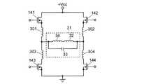
図5は、特許文献1に記載の、自励発振を用いた高周波電源装置の概略構成図である。即ち、この回路では、4個のMOSFET141、142、143、144がフルブリッジ回路を構成し、このフルブリッジ回路から負荷結合インダクタ301、302、303、304を介して、誘導コイル32及びコンデンサ33を含むLC共振回路31に電力が供給される。それによってLC共振回路31に流れる電流は、トランス(誘導結合部)の1次巻線34により検出され、図示しないフィードバック経路を通して各MOSFET141〜144のゲート端子にそれぞれフィードバックされる。このような自励発振回路では、プラズマ状態の変化に伴って誘導コイル32のインピーダンスが変化すると、LC共振回路31の共振周波数が自動的に変化する。このため、外部から特別な制御や指示を何ら行うことなく、フルブリッジ回路側から見た負荷インピーダンスが常に最適な関係に保たれ、高い効率で発振を継続させることができるという利点がある。 FIG. 5 is a schematic configuration diagram of a high-frequency power supply device using self-excited oscillation described in Patent Document 1. That is, in this circuit, four
ところで、ICP発光分析装置では、大気圧雰囲気の下でプラズマを生成させるため、特にプラズマの点灯を開始させる際に、定常的な点灯中に比べて大きな高周波電流を誘導コイルに供給する必要がある。プラズマの点灯特性、つまり点灯のし易さ又はしにくさは、プラズマ生成用ガスの流量、プラズマ生成用ガスの純度、プラズマトーチ形状、プラズマスタンドが置かれた雰囲気、等の影響を受ける。そのため、安定的で良好なプラズマ点灯特性を維持するには、上記のような様々な要因の変動やばらつきを見込んだ上で、十分に余裕のある高周波電流を誘導コイルに供給する必要がある。図5に示した従来の回路において誘導コイル32への電流を増加させるには、電源電圧+Vccを増加させる必要がある。 By the way, in the ICP emission analysis apparatus, since plasma is generated under an atmospheric pressure atmosphere, it is necessary to supply a large high-frequency current to the induction coil as compared with that during steady lighting, particularly when plasma lighting is started. . The lighting characteristics of plasma, that is, the ease or difficulty of lighting, is affected by the flow rate of the plasma generating gas, the purity of the plasma generating gas, the shape of the plasma torch, the atmosphere in which the plasma stand is placed, and the like. Therefore, in order to maintain stable and good plasma lighting characteristics, it is necessary to supply a sufficiently high-frequency current to the induction coil in consideration of fluctuations and variations in various factors as described above. In order to increase the current to the
ただし、電源電圧+Vccはフルブリッジ回路に使用される半導体スイッチング素子(図5の例ではMOSFET141〜144)の定格電圧の制約を受けるため、電源電圧+Vccを上げることで安定したプラズマ点灯特性を確保するには、電源電圧+Vccの増加に耐え得るような定格電圧の大きな半導体スイッチング素子を使用しなければならない。しかしながら、定格電圧の大きな半導体スイッチング素子はオン抵抗が大きくなるため、高周波電源装置における電力損失の増加に繋がるおそれがある。 However, since the power supply voltage + Vcc is restricted by the rated voltage of the semiconductor switching elements (
本発明はこうした課題に鑑みてなされたものであり、その目的とするところは、フルブリッジ回路又はハーフブリッジ回路などのスイッチング回路に使用される半導体スイッチング素子の定格電圧を抑えながら、つまり、オン抵抗の小さい半導体スイッチング素子を使用しながら、プラズマ点灯特性の安定性を維持し、特にプラズマ点灯を安定的に開始させることができる高周波電源装置を提供することにある。 The present invention has been made in view of these problems, and its object is to suppress the rated voltage of a semiconductor switching element used in a switching circuit such as a full bridge circuit or a half bridge circuit, that is, an on-resistance. An object of the present invention is to provide a high-frequency power supply device that can maintain the stability of plasma lighting characteristics while using a semiconductor switching element having a small size, and that can start plasma lighting stably.
上記課題を解決するために成された本発明は、直流電圧源と、プラズマ生成用の誘導コイルとコンデンサとを含むLC共振回路と、前記直流電圧源から供給される直流電力をスイッチングして前記LC共振回路に与える半導体スイッチング素子を含むスイッチング回路と、を具備し、前記誘導コイルに高周波電力を投入することで大気圧雰囲気の下でプラズマを生成するICP発光分析装置用高周波電源装置において、
a)前記スイッチング回路と前記LC共振回路との間に介挿され、インダクタと、並列接続された複数のコンデンサと、該複数のコンデンサの一部をその並列接続から切り離すスイッチング素子と、を含み、該スイッチング素子により前記複数のコンデンサの接続を切り替えてコンデンサの容量を変化させることでインピーダンス変換率を複数段階に切り替え可能であるとともに、前記スイッチング素子の切替えを制御する信号の変化を鈍化させる時定数回路を含むインピーダンス変換部と、
b)プラズマ点灯開始前とその点灯開始後の定常的な点灯時とで前記インピーダンス変換率を切り替えるように前記インピーダンス変換部を動作させる制御部であり、プラズマが消灯している状態から点灯を開始させるときには前記インピーダンス変換部におけるコンデンサの容量を相対的に大きくして前記LC共振回路へ相対的に大きな電流を供給し、プラズマが点灯して定常的な状態になるとコンデンサの容量を相対的に小さく切り替える制御部と、
を備えることを特徴としている。
In order to solve the above problems, the present invention provides a DC voltage source, an LC resonance circuit including an induction coil and a capacitor for generating plasma, and DC power supplied from the DC voltage source to switch the DC power source. A switching circuit including a semiconductor switching element for supplying to an LC resonance circuit, and a high-frequency power supply for an ICP emission spectrometer that generates plasma under an atmospheric pressure atmosphere by applying high-frequency power to the induction coil,
a) inserted between the switching circuit and the LC resonance circuit, including an inductor,a plurality of capacitorsconnected in parallel , and aswitching element that disconnects a part of the plurality of capacitors from the parallel connection; The switching element can switch the connection of the plurality of capacitors to change the capacitance of the capacitor to change the impedance conversion rate in a plurality of stages,and the time constant for slowing the change in the signal for controlling the switching of the switching element An impedance converterincluding a circuit ;
b) A control unit that operates the impedance conversion unit so as to switch the impedance conversion rate before starting plasma lighting and during steady lighting after starting lighting, and starts lighting from a state in which the plasma is extinguished. When the capacitor is used, the capacitance of the capacitor in the impedance converter is relatively increased to supply a relatively large current to the LC resonance circuit. A control unit for switching;
It is characterized by having.
本発明に係る高周波電源装置において、上記スイッチング回路は例えば、複数の半導体スイッチング素子を用いたハーフブリッジ回路又はフルブリッジ回路とすることができる。また、この半導体スイッチング素子としては、典型的には、電力用のMOSFETを用いればよい。 In the high frequency power supply device according to the present invention, the switching circuit can be, for example, a half bridge circuit or a full bridge circuit using a plurality of semiconductor switching elements. As this semiconductor switching element, typically, a power MOSFET may be used.
インピーダンス変換部に含まれる回路素子(インダクタ、コンデンサ)の定数によって決まる複数段階のインピーダンス変換率の一つは、プラズマを定常的に点灯させているときにスイッチング回路から供給される電力が最も効率良くプラズマに投入されるように、つまりプラズマ生成時の電力効率が最大になるように予め調整される。通常、これはインピーダンス整合が最適な状態である。本発明に係る高周波電源装置において、制御部は、プラズマが点灯している期間中に、このようなインピーダンス変換率になるようにインピーダンス変換部のコンデンサの容量を設定する。したがって、プラズマ点灯中には、電力損失を抑え効率的にプラズマ生成状態を維持することができる。
One of the multi-stage impedance conversion rates determined by the constants of the circuit elements(inductors and capacitors) included in the impedance converter is that the power supplied from the switching circuit is most efficient when the plasma is lit constantly. It is adjusted in advance so as to be put into the plasma, that is, to maximize the power efficiency during plasma generation. This is usually the optimal state of impedance matching. In the high frequency power supply device according to the present invention, the control unit sets thecapacitance of thecapacitor of the impedance conversion unit so as to have such an impedance conversion rate during a period in which the plasma is lit. Therefore, the plasma generation state can be maintained efficiently while suppressing power loss during plasma lighting.
これに対し、プラズマが消灯している状態からプラズマの点灯を開始させるときには、制御部は、より大きな電流をLC共振回路に供給することが可能であるようなインピーダンス変換率となるようにインピーダンス変換部のコンデンサの容量を設定する。このときのインピーダンス変換率つまりコンデンサ容量値も、予め実験等により決めておくことができる。即ち、本発明に係る高周波電源装置では、プラズマ点灯開始時に、スイッチング回路等の電源電圧を増加させることなく、LC共振回路に含まれる誘導コイルに大きな高周波電流を流すことができる。これにより、ICP発光分析装置においてプラズマトーチに大きな交番磁場が発生し、それによってプラズマガス雰囲気中に強い誘導電場が形成される。その結果、プラズマガスの電離が起こり易くなり、安定的にプラズマ点灯が開始される。
In contrast, when starting the plasma from the state where the plasma is extinguished, the control unit converts the impedance so that the impedance conversion rate is such that a larger current can be supplied to the LC resonance circuit. Set thecapacitorcapacity . The impedance conversion rate, that is, thecapacitor capacitance value at this timecan also be determined in advance by experiments or the like. That is, in the high frequency power supply device according to the present invention, a large high frequency current can be passed through the induction coil included in the LC resonance circuit without increasing the power supply voltage of the switching circuit or the like at the start of plasma lighting. As a result, a large alternating magnetic field is generatedin the plasma torch in the ICP emission spectrometer, thereby forming a strong induction electric field in the plasma gas atmosphere. As a result, ionization of plasma gas is likely to occur, and plasma lighting is started stably.
ただし、プラズマが点灯した後にインピーダンス変換部のインピーダンス変換率が急に切り替えられると、具体的にはステップ的に切り替えられると、プラズマが消灯するおそれがある。そこで、本発明においてインピーダンス変換部は、並列接続されたコンデンサと、該コンデンサの一部をその並列接続から切り離すスイッチング素子と、を含み、さらに、該スイッチング素子の切替えを制御する信号の変化を鈍化させる時定数回路を備えている。該時定数回路としては例えばRC回路などのローパスフィルタを用いればよい。
However, if the impedance conversion rate of the impedance converter is suddenly switched after the plasma is turned on, specifically, the plasma may be extinguished if it is switched stepwise. Therefore,Oite impedance converting section to the invention comprises a capacitor connected in parallel, a switching element for disconnecting a part of the capacitor from the parallel connection, the further variation of the signal for controlling the switching of the switching element It has a time constant circuit that slows down. As the time constant circuit, for example, a low pass filter such as an RC circuit may be used.
このため、プラズマ点灯が開始した後にインピーダンス変換部におけるインピーダンス変換率が切り替えられる際に、コンデンサの容量が急変せず、或る程度緩慢に変化する。それによって、誘導コイルに供給される電流の変化も緩慢になり、その変化によるプラズマの消灯を防止することができる。
For thisreason , when the impedance conversion rate in the impedance conversion unit is switched after the plasma lighting is started, the capacitance of the capacitor does not change suddenly and changes somewhat slowly. Thereby, the change in the current supplied to the induction coil also becomes slow, and it is possible to prevent the plasma from being extinguished due to the change.
本発明に係る高周波電源装置によれば、誘導コイルを含むLC共振回路に電力を供給するスイッチング回路の電源電圧を増加させることなく、プラズマ点灯開始時に誘導コイルに大きな高周波電流を流し、安定的にプラズマを生成することができる。また、プラズマ点灯中には、電力の利用効率が最良又はそれに近い状態に維持されるようにすることができる。 According to the high-frequency power supply device of the present invention, a large high-frequency current is allowed to flow through the induction coil at the start of plasma lighting without increasing the power supply voltage of the switching circuit that supplies power to the LC resonance circuit including the induction coil. Plasma can be generated. In addition, during plasma lighting, the power use efficiency can be maintained at or near the best.
以下、本発明の一実施例として、ICP発光分析装置のプラズマ生成用に用いられる高周波電源装置について、添付図面を参照しつつ説明する。図1は本実施例の高周波電源装置の概略構成図である。 Hereinafter, as one embodiment of the present invention, a high frequency power supply device used for plasma generation of an ICP emission analyzer will be described with reference to the accompanying drawings. FIG. 1 is a schematic configuration diagram of a high-frequency power supply device according to this embodiment.
ICP発光分析装置のプラズマトーチ(図示せず)中にプラズマを生成するべく該プラズマトーチに巻回された誘導コイル21が、この高周波電源装置において高周波電流を供給する対象である。誘導コイル21には、コンデンサ20とフィードバック用トランスの1次巻線(実際にはこの1次巻線は4個であるが図1では省略して1個のみ記載している)22とが直列に接続されており、これによりLC共振回路19が形成されている。なお、フィードバック用トランスの1次巻線22によるインダクタンスに比べて誘導コイル21のインダクタンスは十分に大きいので、LC共振回路19の共振周波数を決めるインダクタンスは誘導コイル21のインダクタンスが支配的である。 An
直流電源11は例えばダイオードブリッジ回路などの整流回路を含み、外部の商用交流電源10から供給される交流電力に基づいて所定の直流電圧を出力する。この直流電源11の出力端には、並列接続されたコンデンサ12を介してフルブリッジ駆動回路13が接続されている。フルブリッジ駆動回路13は、2個のMOSFET141、143の直列回路と同じく2個のMOSFET142、144の直列回路とが並列に接続された構成である。4個のMOSFET141〜144のゲート端子とソース端子との間にはそれぞれ、フィードバック用トランスの1次巻線22と磁気的に結合する2次巻線(図示せず)を含むMOSFET駆動回路151〜154が接続されている。 The
フルブリッジ駆動回路13とLC共振回路19とは、極性が相違する第1、第2リアクタンス素子17、18を含むインピーダンス変換回路16を介して接続されており、それによって、フルブリッジ駆動回路13においてMOSFET141とMOSFET144、又は、MOSFET142とMOSFET143がオンしたときに、フルブリッジ駆動回路13から第1、第2リアクタンス素子17、18に電流が流れるループが形成される。 The full
本実施例の高周波電源装置では、第1リアクタンス素子17はインダクタであり、第2リアクタンス素子18はコンデンサであるので、以下の説明では、インダクタ17、コンデンサ18と記す。直流電源11からフルブリッジ駆動回路13へ印加される電圧、つまりフルブリッジ駆動回路13の電源電圧が一定である場合、インダクタ17のインダクタンスLと、コンデンサ18の容量Cと、プラズマ投入電力との関係は図3に示すようになる。 In the high frequency power supply device of the present embodiment, the first reactance element 17 is an inductor and the
直流電源11からフルブリッジ駆動回路13へ印加される電圧の最適値はMOSFET141〜144の定格特性に依存するから、この定格特性に応じて直流電源11の出力電圧を定めておくようにする。そして、その条件の下で、インダクタ17のインダクタンスLの値は、コンデンサ18の容量Cの値を所定範囲内で変化させたときのプラズマ投入電力の最大値が要求される値(仕様値)を満足するように設定される。通常、適正な電源電圧において必要以上にプラズマ投入電力が大きくなるのは好ましくないため、最適な電源電圧のときに、プラズマ投入電力の最大値が仕様値を若干上回る程度にインダクタンスを決めるとよい。こうしたことから、例えば図3の例では、インダクタンスLはL2に決められる。 Since the optimum value of the voltage applied from the
図4は、インダクタ17のインダクタンスLが或る値(例えば上述したL2)に定められたときの、コンデンサ18の容量Cとプラズマ生成時の電力効率との関係を示す図である。即ち、コンデンサ18の容量CがC1であるときにプラズマ生成時の電力効率は最大となる。一般的には、これはインピーダンス変換回路16におけるインピーダンス変換作用によってインピーダンス整合がとれている(最適である)状態であると推定される。ただし、コンデンサ18の容量CをC1とした場合には、プラズマ点灯開始時に確実な点灯を行うのに十分な誘導コイル電流を確保できない可能性がある。一方、コンデンサ18の容量CをC1よりも大きなC2とすると、プラズマ生成時の電力効率は下がるものの、プラズマ点灯開始時に誘導コイル21への供給電流が増大し、プラズマ点灯開始時の点灯特性が良好になる。
FIG. 4 is a diagram showing the relationship between the capacitance C of the
そこで、本実施例の高周波電源装置では、インピーダンス変換回路16におけるコンデンサ18の容量Cの値がC1とC2とで切り替え可能な構成となっており、プラズマの点灯を制御する制御部24の指示の下に、切替駆動部23がインピーダンス変換回路16におけるコンデンサ18の容量Cを切り替える。インダクタ17のインダクタンスLは不変でコンデンサ18の容量Cのみが変化するので、これはインピーダンス変換回路16におけるインピーダンス変換率が変化することを意味する。具体的に、制御部24は以下のような制御を行う。 Therefore, in the high frequency power supply device of the present embodiment, the value of the capacitance C of the
即ち、プラズマが消灯している状態から点灯を開始させるときに、制御部24は、インピーダンス変換回路16におけるコンデンサ18の容量CがC2になるように切替駆動部23に指示を与える。これにより、インピーダンス変換回路16におけるインピーダンス変換率は、プラズマ生成開始前に、より大きな高周波電流をLC共振回路19に供給できる状態に設定される。その結果、プラズマ点灯時に誘導コイル21に大きな高周波電流が流れ、プラズマトーチに大きな交番磁場が発生し、それによってプラズマガス雰囲気中に強い誘導電場が形成される。その結果、プラズマガスの電離が起こり易くなり、安定的にプラズマ点灯が開始される。 That is, when the lighting is started from the state where the plasma is extinguished, the
プラズマが点灯してから例えば所定時間が経過すると、制御部24は、インピーダンス変換回路16におけるコンデンサ18の容量CがC2からC1に切り替わるように切替駆動部23に指示を与える。これにより、インピーダンス変換回路16におけるインピーダンス変換率は、プラズマ生成時の電力効率がほぼ最適である状態に設定される。これにより、効率よくエネルギをプラズマに投入し、安定的にプラズマを維持することができる。 For example, when a predetermined time elapses after the plasma is turned on, the
図2は図1中のインピーダンス変換回路16及び切替駆動部23の詳細回路の一例である。図1中のインダクタ17は、図2中の第1インダクタ17a及び第2インダクタ17bに相当し、同じく図1中のコンデンサ18は、図2中のコンデンサ18a、及び、これに並列に接続された、二つのコンデンサ18b、18c、PINダイオード18dの直列接続回路、に相当する。ここで、PINダイオード18dはスイッチング素子として機能し、PINダイオード18dが実質的にオン状態であるときには、コンデンサ18b、18cを含む直列接続回路はコンデンサ18aに並列に接続され、PINダイオード18dが実質的にオフ状態であるときには、コンデンサ18b、18cを含む直列接続回路は機能せず、コンデンサ18aのみがリアクタンス素子として有効になる。 FIG. 2 is an example of a detailed circuit of the
周知のようにPINダイオードは高周波領域において抵抗を含む等価回路で表され、直流バイアスによってその等価抵抗が変化する。本実施例の高周波電源装置では、このことを利用し、PINダイオード18dの直流バイアスを切り替えることで、上述したようなコンデンサ18の容量Cの切替えを実現している。 As is well known, the PIN diode is represented by an equivalent circuit including a resistor in a high frequency region, and the equivalent resistance is changed by a DC bias. In the high-frequency power supply device of the present embodiment, this is utilized to switch the capacitance C of the
具体的に説明すると、図2に示すように、切替駆動部23は、PINダイオード18dのアノード端子、カソード端子にそれぞれ一端が接続された二つのインダクタ231、232、その二つのインダクタ231、232の他端の間に接続されたコンデンサ233、インダクタ231の他端と負の電源電圧VDC2との間に接続された抵抗234、ソース電位がCOM電位にフローティングされたMOSFET238、制御部(図2中には図示せず)から送られる制御信号を受けてMOSFET238に信号(MOSFETをオン又はオフさせる信号)を伝達するフォトカプラ241、及び、MOSFET238のソース端子と上記インダクタ231との間に接続された抵抗236、を含む。 More specifically, as shown in FIG. 2, the switching
制御部から制御信号がフォトカプラ241に入力され、該フォトカプラ241の出力端から所定の電圧(二値論理の論理「1」に相当する電圧)が出力されるとMOSFET238はオンし、MOSFET238のソース端子と抵抗236との接続点の電位はほぼVDC1になる。このため、インダクタ231とコンデンサ233との接続点Pの電位は、正極性であるVDC1と負極性であるVDC2との電位差を抵抗236、234で分圧した電位となる。抵抗236の抵抗値を抵抗234の抵抗値よりも充分小さくしておくと、上記接続点Pの電位は、PINダイオード18dを順方向バイアスする電位となり、PINダイオード18dはオンして、コンデンサ18b、18cの直列回路がコンデンサ18aに並列接続される。これによって、インピーダンス変換回路16におけるコンデンサ18の容量は相対的に大きくなる。これが、図4においてコンデンサ18の容量CがC2である状態である。 When a control signal is input from the control unit to the
制御部からフォトカプラ241に供給される電流が遮断されると、フォトカプラ241出力端の電圧は二値論理の論理「0」に相当する電圧に下がり、MOSFET238はオフする。すると、抵抗236は実質的に存在しないものとみなせ、インダクタ231とコンデンサ233との接続点Pは抵抗234を介して負極性であるVDC2と接続される。そのため、この接続点Pの電位は負になり、PINダイオード18dは逆方向バイアスされてオフする。その結果、コンデンサ18b、18cの直列回路自体が存在しないものとみなせ、インピーダンス変換回路16におけるコンデンサ18の容量は相対的に小さくなる。これが、図4においてコンデンサ18の容量CがC1である状態である。 When the current supplied from the control unit to the
以上のようにして、切替駆動部23はインピーダンス変換回路16におけるコンデンサ18の容量Cを2段階に切り替えることができる。このようなPINダイオード18dのオン・オフの切替えによって容量Cは切り替えられるが、その際に、抵抗234とコンデンサ233はローパスフィルタによる時定数回路として機能する。即ち、MOSFET238のオン・オフの切替えによってMOSFET238のソース端子の電位は急に変化するが、インダクタ231とコンデンサ233との接続点Pの電位の変化は、時定数回路の時定数に応じて緩慢になる。その結果、コンデンサ18の容量Cの変化も緩慢になり、インピーダンス変換回路16のインピーダンス変換率が急変する(ステップ的に切り替わる)ことによるプラズマの消灯現象を回避することができる。 As described above, the switching
なお、上記実施例は本発明の一例であり、本発明の趣旨の範囲で適宜変形、修正、追加などを行っても本願特許請求の範囲に包含されることは当然である。 The above-described embodiment is an example of the present invention, and it is a matter of course that modifications, additions, additions, and the like as appropriate within the scope of the present invention are included in the scope of the claims of the present application.
例えば、図1、図2に示した回路構成は一例であり、上述したような動作を実行可能な回路がこれら図面に記載の例に限らないことは当業者には常識である。また上記実施例ではLC共振回路を駆動するスイッチング回路としてフルブリッジ駆動回路を用いているが、ハーフブリッジ駆動回路などの他の構成のスイッチング回路を用いてもよい。 For example, the circuit configurations shown in FIGS. 1 and 2 are examples, and it is common knowledge to those skilled in the art that the circuits capable of executing the operations described above are not limited to the examples described in these drawings. In the above embodiment, the full bridge drive circuit is used as the switching circuit for driving the LC resonance circuit, but a switching circuit having another configuration such as a half bridge drive circuit may be used.
10…商用交流電源
11…直流電源
12、18a、18b、18c、20、233…コンデンサ
13…フルブリッジ駆動回路
141〜144、238…MOSFET
151〜154…MOSFET駆動回路
16…インピーダンス変換回路
17…第1リアクタンス素子(インダクタ)
17a…第1インダクタ
17b…第2インダクタ
18…第2リアクタンス素子(コンデンサ)
18d…PINダイオード
19…LC共振回路
21…誘導コイル
22…1次巻線
23…切替駆動部
231、232…インダクタ
234、236…抵抗
241…フォトカプラ
24…制御部DESCRIPTION OF
151 to 154...
17a ...
18d ...
Claims (3)
Translated fromJapanesea)前記スイッチング回路と前記LC共振回路との間に介挿され、インダクタと、並列接続された複数のコンデンサと、該複数のコンデンサの一部をその並列接続から切り離すスイッチング素子と、を含み、該スイッチング素子により前記複数のコンデンサの接続を切り替えてコンデンサの容量を変化させることでインピーダンス変換率を複数段階に切り替え可能であるとともに、前記スイッチング素子の切替えを制御する信号の変化を鈍化させる時定数回路を含むインピーダンス変換部と、
b)プラズマ点灯開始前とその点灯開始後の定常的な点灯時とで前記インピーダンス変換率を切り替えるように前記インピーダンス変換部を動作させる制御部であり、プラズマが消灯している状態から点灯を開始させるときには前記インピーダンス変換部におけるコンデンサの容量を相対的に大きくして前記LC共振回路へ相対的に大きな電流を供給し、プラズマが点灯して定常的な状態になるとコンデンサの容量を相対的に小さく切り替える制御部と、
を備えることを特徴とするICP発光分析装置用高周波電源装置。An LC resonance circuit including a DC voltage source, an induction coil and a capacitor for generating plasma, and a switching circuit including a semiconductor switching element that switches DC power supplied from the DC voltage source and applies the LC power to the LC resonance circuit; A high frequency power supply for an ICP emission analyzer that generates plasma under an atmospheric pressure atmosphere by applying high frequency power to the induction coil,
a) inserted between the switching circuit and the LC resonance circuit, including an inductor,a plurality of capacitorsconnected in parallel , and aswitching element that disconnects a part of the plurality of capacitors from the parallel connection; The switching element can switch the connection of the plurality of capacitors to change the capacitance of the capacitor to change the impedance conversion rate in a plurality of stages,and the time constant for slowing the change in the signal for controlling the switching of the switching element An impedance converterincluding a circuit ;
b) A control unit that operates the impedance conversion unit so as to switch the impedance conversion rate before starting plasma lighting and during steady lighting after starting lighting, and starts lighting from a state in which the plasma is extinguished. When the capacitor is used, the capacitance of the capacitor in the impedance converter is relatively increased to supply a relatively large current to the LC resonance circuit. A control unit for switching;
A high-frequency power supply device for an ICP emission analyzer, comprising:
前記制御部は、プラズマが定常的な状態になり前記コンデンサの容量を相対的に小さく切り替える際に、プラズマ生成における電力効率が最大となるようにインピーダンス変換率を設定して誘導コイルに対するインピーダンスを整合させることを特徴とするICP発光分析装置用高周波電源装置。A high-frequency power supply device for an ICP emission analyzer according to claim 1,
When the plasma is in a steady state and the capacitance of the capacitor is switched to a relatively small value, the control unit sets the impedance conversion rate so that the power efficiency in plasma generation is maximized and matches the impedance to the induction coil. A high frequency power supply device for an ICP emission analyzer characterized by comprising:
前記制御部は、プラズマが点灯してから所定時間が経過したときに前記コンデンサの容量を相対的に小さく切り替えることを特徴とするICP発光分析装置用高周波電源装置。A high-frequency power supply device for an ICP emission analyzer according to claim 1 or 2,
The high frequency power supply apparatus for an ICP emission analysis apparatus, wherein the control unit switches the capacitance of the capacitor to be relatively small when a predetermined time has elapsed after the plasma is turned on.
Priority Applications (3)
| Application Number | Priority Date | Filing Date | Title |
|---|---|---|---|
| JP2014040543AJP6413261B2 (en) | 2014-03-03 | 2014-03-03 | High frequency power supply for ICP emission analyzer |
| US14/635,152US10327322B2 (en) | 2014-03-03 | 2015-03-02 | Radio-frequency power unit |
| CN201510094746.8ACN104901580B (en) | 2014-03-03 | 2015-03-03 | High intensity light source |
Applications Claiming Priority (1)
| Application Number | Priority Date | Filing Date | Title |
|---|---|---|---|
| JP2014040543AJP6413261B2 (en) | 2014-03-03 | 2014-03-03 | High frequency power supply for ICP emission analyzer |
Publications (2)
| Publication Number | Publication Date |
|---|---|
| JP2015167070A JP2015167070A (en) | 2015-09-24 |
| JP6413261B2true JP6413261B2 (en) | 2018-10-31 |
Family
ID=54007410
Family Applications (1)
| Application Number | Title | Priority Date | Filing Date |
|---|---|---|---|
| JP2014040543AActiveJP6413261B2 (en) | 2014-03-03 | 2014-03-03 | High frequency power supply for ICP emission analyzer |
Country Status (3)
| Country | Link |
|---|---|
| US (1) | US10327322B2 (en) |
| JP (1) | JP6413261B2 (en) |
| CN (1) | CN104901580B (en) |
Families Citing this family (9)
| Publication number | Priority date | Publication date | Assignee | Title |
|---|---|---|---|---|
| US11615943B2 (en) | 2017-07-07 | 2023-03-28 | Advanced Energy Industries, Inc. | Inter-period control for passive power distribution of multiple electrode inductive plasma source |
| US11651939B2 (en) | 2017-07-07 | 2023-05-16 | Advanced Energy Industries, Inc. | Inter-period control system for plasma power delivery system and method of operating same |
| KR102504624B1 (en) | 2017-07-07 | 2023-02-27 | 어드밴스드 에너지 인더스트리즈 인코포레이티드 | Inter-period control system for plasma power delivery system and method of operating the same |
| WO2020185353A1 (en) | 2019-03-13 | 2020-09-17 | Applied Materials, Inc. | Plasma ignition circuit |
| KR102242234B1 (en)* | 2019-05-08 | 2021-04-20 | 주식회사 뉴파워 프라즈마 | Rf generator and its operating method |
| JP7450387B2 (en)* | 2019-12-27 | 2024-03-15 | 株式会社ダイヘン | Impedance adjustment device |
| JP7465657B2 (en) | 2019-12-27 | 2024-04-11 | 株式会社ダイヘン | Impedance Adjustment Device |
| DE102020104090A1 (en)* | 2020-02-17 | 2021-08-19 | Comet Ag | High-frequency amplifier arrangement for a high-frequency generator |
| WO2022173629A1 (en)* | 2021-02-12 | 2022-08-18 | Advanced Energy Industries, Inc. | Inter-period control for passive power distribution of multiple electrode inductive plasma source |
Family Cites Families (22)
| Publication number | Priority date | Publication date | Assignee | Title |
|---|---|---|---|---|
| US5815047A (en)* | 1993-10-29 | 1998-09-29 | Applied Materials, Inc. | Fast transition RF impedance matching network for plasma reactor ignition |
| JPH1019782A (en)* | 1996-07-03 | 1998-01-23 | Shimadzu Corp | ICP analyzer |
| US5945785A (en)* | 1996-08-27 | 1999-08-31 | Matsushita Electric Works, Ltd. | Power source device with minimized variation in circuit efficiency due to variation in applied voltage to driving transformer |
| US6424232B1 (en)* | 1999-11-30 | 2002-07-23 | Advanced Energy's Voorhees Operations | Method and apparatus for matching a variable load impedance with an RF power generator impedance |
| US6472822B1 (en)* | 2000-04-28 | 2002-10-29 | Applied Materials, Inc. | Pulsed RF power delivery for plasma processing |
| JP2002184598A (en)* | 2000-12-12 | 2002-06-28 | Shimadzu Corp | High frequency power supply for ICP |
| JP4772232B2 (en)* | 2001-08-29 | 2011-09-14 | アジレント・テクノロジーズ・インク | High frequency amplifier circuit and driving method of high frequency amplifier circuit |
| TWI425767B (en)* | 2005-10-31 | 2014-02-01 | Mks Instr Inc | Radio frequency power delivery system |
| EP2020016B1 (en)* | 2006-05-22 | 2019-06-26 | Agilent Technologies Australia (M) Pty Ltd | Power generator for spectrometry |
| US20080003702A1 (en)* | 2006-06-28 | 2008-01-03 | Cruse James P | Low Power RF Tuning Using Optical and Non-Reflected Power Methods |
| JP2008202990A (en)* | 2007-02-16 | 2008-09-04 | Shimadzu Corp | High frequency power supply for ICP |
| US8390394B2 (en)* | 2007-12-19 | 2013-03-05 | Soshin Electric Co., Ltd. | High frequency switch |
| US8692466B2 (en)* | 2009-02-27 | 2014-04-08 | Mks Instruments Inc. | Method and apparatus of providing power to ignite and sustain a plasma in a reactive gas generator |
| JP5241578B2 (en)* | 2009-03-19 | 2013-07-17 | 株式会社日清製粉グループ本社 | Induction thermal plasma generation method and apparatus |
| CN103222344B (en)* | 2010-09-22 | 2015-12-16 | 株式会社岛津制作所 | High-frequency power supply device |
| US8436643B2 (en)* | 2010-11-04 | 2013-05-07 | Advanced Energy Industries, Inc. | High frequency solid state switching for impedance matching |
| TWI455172B (en)* | 2010-12-30 | 2014-10-01 | Semes Co Ltd | Adjustable capacitor, plasma impedance matching device, plasma impedance mathching method, and substrate treating apparatus |
| US8416008B2 (en)* | 2011-01-20 | 2013-04-09 | Advanced Energy Industries, Inc. | Impedance-matching network using BJT switches in variable-reactance circuits |
| JP2013098177A (en)* | 2011-10-31 | 2013-05-20 | Semes Co Ltd | Substrate processing device and impedance matching method |
| JP5534366B2 (en)* | 2012-06-18 | 2014-06-25 | 株式会社京三製作所 | High frequency power supply device and ignition voltage selection method |
| JP6353223B2 (en)* | 2013-12-20 | 2018-07-04 | 東京エレクトロン株式会社 | Plasma processing method and plasma processing apparatus |
| US10699880B2 (en)* | 2015-06-29 | 2020-06-30 | Reno Technologies, Inc. | Voltage reduction circuit |
- 2014
- 2014-03-03JPJP2014040543Apatent/JP6413261B2/enactiveActive
- 2015
- 2015-03-02USUS14/635,152patent/US10327322B2/enactiveActive
- 2015-03-03CNCN201510094746.8Apatent/CN104901580B/enactiveActive
Also Published As
| Publication number | Publication date |
|---|---|
| CN104901580B (en) | 2018-11-27 |
| US10327322B2 (en) | 2019-06-18 |
| JP2015167070A (en) | 2015-09-24 |
| US20150250046A1 (en) | 2015-09-03 |
| CN104901580A (en) | 2015-09-09 |
Similar Documents
| Publication | Publication Date | Title |
|---|---|---|
| JP6413261B2 (en) | High frequency power supply for ICP emission analyzer | |
| US10923952B2 (en) | Secondary-side output boost technique in power converters and wireless power transfer systems | |
| JP5174013B2 (en) | Generator for spectroscopic analysis | |
| US11069499B2 (en) | Power-saving circuit for contactor | |
| CN109842973B (en) | Power distribution system | |
| US9232627B2 (en) | Radio-frequency oscillation circuit | |
| JP2010114001A (en) | Power source device for plasma generation | |
| KR20140145830A (en) | Power supplying device | |
| CN101242144B (en) | A method of controlling a DC-DC converter | |
| JP4434204B2 (en) | Power supply | |
| KR100639483B1 (en) | electrodeless discharge lamp electric source apparatus | |
| KR20200100811A (en) | Resonance matching circuit | |
| JP2012175809A (en) | Switching power supply unit | |
| JP6341182B2 (en) | Power supply | |
| JP4949285B2 (en) | Plasma discharge device | |
| JP6782474B2 (en) | Thermoelectric conversion element output control device | |
| JP6041532B2 (en) | Electronic load device | |
| JP7650219B2 (en) | DC/DC converter and power supply device | |
| CN104955253B (en) | A kind of fluorescent lamp drive circuit | |
| JP2007267581A (en) | Power-factor improved type dc stabilization switching power supply | |
| JP4723343B2 (en) | Discharge lamp lighting device | |
| TW202345498A (en) | Power supply device and laser device which has a laser resonator that is capable of effectively suppressing overvoltage using only hardware | |
| HK40009555B (en) | Power distribution system | |
| GB2472038A (en) | Power adaptor for discharge light source | |
| JP2014099309A (en) | Lighting device and lighting fixture |
Legal Events
| Date | Code | Title | Description |
|---|---|---|---|
| A621 | Written request for application examination | Free format text:JAPANESE INTERMEDIATE CODE: A621 Effective date:20160701 | |
| A977 | Report on retrieval | Free format text:JAPANESE INTERMEDIATE CODE: A971007 Effective date:20170628 | |
| A131 | Notification of reasons for refusal | Free format text:JAPANESE INTERMEDIATE CODE: A131 Effective date:20170704 | |
| A521 | Request for written amendment filed | Free format text:JAPANESE INTERMEDIATE CODE: A523 Effective date:20170904 | |
| A131 | Notification of reasons for refusal | Free format text:JAPANESE INTERMEDIATE CODE: A131 Effective date:20180130 | |
| A521 | Request for written amendment filed | Free format text:JAPANESE INTERMEDIATE CODE: A523 Effective date:20180330 | |
| TRDD | Decision of grant or rejection written | ||
| A01 | Written decision to grant a patent or to grant a registration (utility model) | Free format text:JAPANESE INTERMEDIATE CODE: A01 Effective date:20180904 | |
| A61 | First payment of annual fees (during grant procedure) | Free format text:JAPANESE INTERMEDIATE CODE: A61 Effective date:20180917 | |
| R151 | Written notification of patent or utility model registration | Ref document number:6413261 Country of ref document:JP Free format text:JAPANESE INTERMEDIATE CODE: R151 |