JP6393619B2 - Multilayer printed wiring board manufacturing method and base substrate - Google Patents
Multilayer printed wiring board manufacturing method and base substrateDownload PDFInfo
- Publication number
- JP6393619B2 JP6393619B2JP2014539856AJP2014539856AJP6393619B2JP 6393619 B2JP6393619 B2JP 6393619B2JP 2014539856 AJP2014539856 AJP 2014539856AJP 2014539856 AJP2014539856 AJP 2014539856AJP 6393619 B2JP6393619 B2JP 6393619B2
- Authority
- JP
- Japan
- Prior art keywords
- group
- layer
- resin
- release agent
- carrier
- Prior art date
- Legal status (The legal status is an assumption and is not a legal conclusion. Google has not performed a legal analysis and makes no representation as to the accuracy of the status listed.)
- Expired - Fee Related
Links
Images


Classifications
- H—ELECTRICITY
- H01—ELECTRIC ELEMENTS
- H01L—SEMICONDUCTOR DEVICES NOT COVERED BY CLASS H10
- H01L23/00—Details of semiconductor or other solid state devices
- H—ELECTRICITY
- H01—ELECTRIC ELEMENTS
- H01L—SEMICONDUCTOR DEVICES NOT COVERED BY CLASS H10
- H01L23/00—Details of semiconductor or other solid state devices
- H01L23/48—Arrangements for conducting electric current to or from the solid state body in operation, e.g. leads, terminal arrangements ; Selection of materials therefor
- H01L23/488—Arrangements for conducting electric current to or from the solid state body in operation, e.g. leads, terminal arrangements ; Selection of materials therefor consisting of soldered or bonded constructions
- H01L23/498—Leads, i.e. metallisations or lead-frames on insulating substrates, e.g. chip carriers
- H01L23/49822—Multilayer substrates
- H—ELECTRICITY
- H01—ELECTRIC ELEMENTS
- H01L—SEMICONDUCTOR DEVICES NOT COVERED BY CLASS H10
- H01L23/00—Details of semiconductor or other solid state devices
- H01L23/48—Arrangements for conducting electric current to or from the solid state body in operation, e.g. leads, terminal arrangements ; Selection of materials therefor
- H01L23/488—Arrangements for conducting electric current to or from the solid state body in operation, e.g. leads, terminal arrangements ; Selection of materials therefor consisting of soldered or bonded constructions
- H01L23/498—Leads, i.e. metallisations or lead-frames on insulating substrates, e.g. chip carriers
- H01L23/49866—Leads, i.e. metallisations or lead-frames on insulating substrates, e.g. chip carriers characterised by the materials
- H01L23/49894—Materials of the insulating layers or coatings
- H—ELECTRICITY
- H05—ELECTRIC TECHNIQUES NOT OTHERWISE PROVIDED FOR
- H05K—PRINTED CIRCUITS; CASINGS OR CONSTRUCTIONAL DETAILS OF ELECTRIC APPARATUS; MANUFACTURE OF ASSEMBLAGES OF ELECTRICAL COMPONENTS
- H05K3/00—Apparatus or processes for manufacturing printed circuits
- H05K3/0058—Laminating printed circuit boards onto other substrates, e.g. metallic substrates
- H05K3/0061—Laminating printed circuit boards onto other substrates, e.g. metallic substrates onto a metallic substrate, e.g. a heat sink
- H—ELECTRICITY
- H05—ELECTRIC TECHNIQUES NOT OTHERWISE PROVIDED FOR
- H05K—PRINTED CIRCUITS; CASINGS OR CONSTRUCTIONAL DETAILS OF ELECTRIC APPARATUS; MANUFACTURE OF ASSEMBLAGES OF ELECTRICAL COMPONENTS
- H05K3/00—Apparatus or processes for manufacturing printed circuits
- H05K3/0097—Processing two or more printed circuits simultaneously, e.g. made from a common substrate, or temporarily stacked circuit boards
- H—ELECTRICITY
- H05—ELECTRIC TECHNIQUES NOT OTHERWISE PROVIDED FOR
- H05K—PRINTED CIRCUITS; CASINGS OR CONSTRUCTIONAL DETAILS OF ELECTRIC APPARATUS; MANUFACTURE OF ASSEMBLAGES OF ELECTRICAL COMPONENTS
- H05K3/00—Apparatus or processes for manufacturing printed circuits
- H05K3/46—Manufacturing multilayer circuits
- H05K3/4644—Manufacturing multilayer circuits by building the multilayer layer by layer, i.e. build-up multilayer circuits
- H05K3/4682—Manufacture of core-less build-up multilayer circuits on a temporary carrier or on a metal foil
- H—ELECTRICITY
- H01—ELECTRIC ELEMENTS
- H01L—SEMICONDUCTOR DEVICES NOT COVERED BY CLASS H10
- H01L2924/00—Indexing scheme for arrangements or methods for connecting or disconnecting semiconductor or solid-state bodies as covered by H01L24/00
- H01L2924/0001—Technical content checked by a classifier
- H01L2924/0002—Not covered by any one of groups H01L24/00, H01L24/00 and H01L2224/00
- H—ELECTRICITY
- H05—ELECTRIC TECHNIQUES NOT OTHERWISE PROVIDED FOR
- H05K—PRINTED CIRCUITS; CASINGS OR CONSTRUCTIONAL DETAILS OF ELECTRIC APPARATUS; MANUFACTURE OF ASSEMBLAGES OF ELECTRICAL COMPONENTS
- H05K2203/00—Indexing scheme relating to apparatus or processes for manufacturing printed circuits covered by H05K3/00
- H05K2203/01—Tools for processing; Objects used during processing
- H05K2203/0147—Carriers and holders
- H05K2203/0152—Temporary metallic carrier, e.g. for transferring material
Landscapes
- Engineering & Computer Science (AREA)
- Microelectronics & Electronic Packaging (AREA)
- Physics & Mathematics (AREA)
- Condensed Matter Physics & Semiconductors (AREA)
- General Physics & Mathematics (AREA)
- Computer Hardware Design (AREA)
- Power Engineering (AREA)
- Manufacturing & Machinery (AREA)
- Production Of Multi-Layered Print Wiring Board (AREA)
- Laminated Bodies (AREA)
Description
Translated fromJapanese本発明は、多層プリント配線基板の製造方法及びベース基材に関する。 The present invention relates to a method for manufacturing a multilayer printed wiring board and a base substrate.
多層プリント配線基板に関して従来から様々な開発が行われている。例えば、特許文献1には、銅箔のキャリアとしてプリプレグを採用し、プリプレグ上に剥離可能に銅箔を積層した構成が開示されている。 Various developments have been made on multilayer printed wiring boards. For example,
多層プリント配線基板には、1以上の配線層と1以上の絶縁層を含むビルドアップ層が樹脂製のベース基板上に積層した構成が通常含まれるが、樹脂製のベース基板を薄くすると多層プリント配線板が製造工程中で撓んで変形したり、反りが生じたりして実装工程上の支障が起こる場合がある。本願発明は、この点に鑑みて、従来とは異構成の薄型の多層プリント配線板を製造する際に支持体として機能するベース基材を提供することを目的とする。 A multilayer printed wiring board usually includes a configuration in which a build-up layer including one or more wiring layers and one or more insulating layers is laminated on a resin base substrate. In some cases, the wiring board may be bent and deformed during the manufacturing process, or may be warped, thereby hindering the mounting process. In view of this point, an object of the present invention is to provide a base substrate that functions as a support when a thin multilayer printed wiring board having a configuration different from the conventional one is manufactured.
本発明に係る多層プリント配線基板の製造方法は、金属製の板状キャリアの少なくとも1つの主面上に離型剤層を介して樹脂層が積層したベース基材を準備する第1工程と、前記ベース基材の前記樹脂層上に1層以上のビルドアップ層を積層する第2工程と、を含む。 The method for producing a multilayer printed wiring board according to the present invention includes a first step of preparing a base substrate in which a resin layer is laminated via a release agent layer on at least one main surface of a metal plate carrier; And a second step of laminating one or more buildup layers on the resin layer of the base substrate.
前記板状キャリアの基板厚が、5μm以上1600μm以下である、と良い。 The substrate thickness of the plate carrier is preferably 5 μm or more and 1600 μm or less.
前記板状キャリアと前記樹脂層間の剥離強度が、10gf/cm以上200gf/cm以下である、と良い。 The peel strength between the plate carrier and the resin layer is preferably 10 gf / cm or more and 200 gf / cm or less.
220℃で3時間、6時間又は9時間のうちの少なくとも一つの加熱後における、前記板状キャリアと前記樹脂層間の剥離強度が、10gf/cm以上200gf/cm以下である、と良い。 The peel strength between the plate-like carrier and the resin layer after heating at 220 ° C. for 3 hours, 6 hours, or 9 hours is preferably 10 gf / cm or more and 200 gf / cm or less.
前記ビルドアップ層が積層された前記樹脂層と前記板状キャリアとを分離する第3工程を更に含む、と良い。 It is preferable that the method further includes a third step of separating the resin layer on which the buildup layer is laminated and the plate carrier.
前記樹脂層を第1樹脂層とする上記の多層プリント配線基板の製造方法にして、
前記第3工程により得られた前記多層プリント配線基板上に前記第1樹脂層とは異なる第2樹脂層、及び更なるビルドアップ層を積層する第4工程を更に含む、と良い。In the manufacturing method of the above multilayer printed wiring board in which the resin layer is the first resin layer,
Preferably, the method further includes a fourth step of laminating a second resin layer different from the first resin layer and a further build-up layer on the multilayer printed wiring board obtained in the third step.
前記樹脂層が、プリプレグである、と良い。 The resin layer is preferably a prepreg.
前記樹脂層は、120〜320℃のガラス転移温度Tgを有する、と良い。 The resin layer preferably has a glass transition temperature Tg of 120 to 320 ° C.
前記ビルドアップ層が、1以上の絶縁層と1以上の配線層を含む、と良い。 The build-up layer preferably includes one or more insulating layers and one or more wiring layers.
前記ビルドアップ層に含まれる1以上の配線層が、パターニングされた若しくはパターニングされていない金属箔である、と良い。 The one or more wiring layers included in the build-up layer may be a patterned or unpatterned metal foil.
前記ビルドアップ層に含まれる1以上の絶縁層が、プリプレグである、と良い。 One or more insulating layers included in the build-up layer may be a prepreg.
前記ビルドアップ層が、片面あるいは両面金属張積層板を含む、と良い。 The build-up layer preferably includes a single-sided or double-sided metal-clad laminate.
前記ビルドアップ層が、サブトラクティブ法又はフルアディティブ法又はセミアディティブ法の少なくとも一方を用いて形成される、と良い。 The buildup layer may be formed using at least one of a subtractive method, a full additive method, and a semi-additive method.
前記ベース基材上に前記ビルドアップ層が積層した積層体に対してダイシング処理を施す第5工程を更に含む、と良い。 It is preferable that the method further includes a fifth step of performing a dicing process on the laminate in which the buildup layer is laminated on the base substrate.
前記ダイシング処理により、前記ベース基材上に前記ビルドアップ層が積層した前記積層体には1以上の溝が形成され、当該溝により前記ビルドアップ層が個片化可能である、と良い。 It is preferable that one or more grooves are formed in the laminate in which the buildup layer is laminated on the base substrate by the dicing process, and the buildup layer can be separated into pieces by the grooves.
前記ビルドアップ層に含まれる1以上の絶縁層に対してビア配線を形成する第6工程を更に含む、と良い。 Preferably, the method further includes a sixth step of forming a via wiring for one or more insulating layers included in the buildup layer.
前記離型剤層が、次式:
に示すシラン化合物、その加水分解生成物、該加水分解生成物の縮合体を単独で又は複数組み合わせて用いてなる、と良い。The release agent layer has the following formula:
The silane compound, the hydrolysis product thereof, and the condensate of the hydrolysis product may be used alone or in combination.
前記離型剤層が、分子内に2つ以下のメルカプト基を有する化合物を用いてなる、と良い。 The release agent layer is preferably formed using a compound having two or less mercapto groups in the molecule.
前記離型剤層が、次式:
に示すアルミネート化合物、チタネート化合物、ジルコネート化合物、これらの加水分解生成物、該加水分解生成物の縮合体を単独で又は複数組み合わせて用いてなる、と良い。The release agent layer has the following formula:
It is preferable to use the aluminate compound, titanate compound, zirconate compound, the hydrolysis products thereof, and the condensates of the hydrolysis products, which are used alone or in combination.
離型剤層が、シリコーンと、エポキシ系樹脂、メラミン系樹脂及びフッ素樹脂から選択されるいずれか1つ又は複数の樹脂とで構成される樹脂塗膜である、と良い。 The release agent layer may be a resin coating film composed of silicone and any one or a plurality of resins selected from an epoxy resin, a melamine resin, and a fluororesin.
前記板状キャリアが銅又は銅合金からなると良い。 The plate carrier is preferably made of copper or a copper alloy.
前記配線層が銅又は銅合金からなると良い。 The wiring layer is preferably made of copper or a copper alloy.
本発明に係る多層プリント配線基板は、上記の何れかに記載の多層プリント配線基板の製造方法により製造された多層プリント配線基板である。 A multilayer printed wiring board according to the present invention is a multilayer printed wiring board manufactured by the method for manufacturing a multilayer printed wiring board described above.
本発明に係るベース基材は、多層プリント配線基板の製造方法に用いられるベース基材であって、金属製の板状キャリアと、前記板状キャリアの少なくとも1つの主面上に形成された離型剤層と、前記離型剤層を介して前記板状キャリア上に積層した樹脂層と、を備え、前記樹脂層と前記板状キャリアとが剥離可能である。 A base substrate according to the present invention is a base substrate used in a method for manufacturing a multilayer printed wiring board, and is a metal plate carrier and a separation formed on at least one main surface of the plate carrier. A mold agent layer and a resin layer laminated on the plate-like carrier via the release agent layer are provided, and the resin layer and the plate-like carrier are peelable.
前記板状キャリアの基板厚が、5μm以上1600μm以下である、と良い。 The substrate thickness of the plate carrier is preferably 5 μm or more and 1600 μm or less.
前記板状キャリアと前記樹脂層間の剥離強度が、10gf/cm以上200gf/cm以下である、と良い。 The peel strength between the plate carrier and the resin layer is preferably 10 gf / cm or more and 200 gf / cm or less.
220℃で3時間、6時間又は9時間のうちの少なくとも一つの加熱後における、前記板状キャリアと前記樹脂層間の剥離強度が、10gf/cm以上200gf/cm以下である、と良い。 The peel strength between the plate-like carrier and the resin layer after heating at 220 ° C. for 3 hours, 6 hours, or 9 hours is preferably 10 gf / cm or more and 200 gf / cm or less.
前記板状キャリアが銅又は銅合金からなると良い。 The plate carrier is preferably made of copper or a copper alloy.
前記樹脂層がプリプレグからなると良い。 The resin layer is preferably made of prepreg.
前記離型剤層が、次式:
に示すシラン化合物、その加水分解生成物、該加水分解生成物の縮合体を単独で又は複数組み合わせて用いてなる、と良い。The release agent layer has the following formula:
The silane compound, the hydrolysis product thereof, and the condensate of the hydrolysis product may be used alone or in combination.
前記離型剤層が、分子内に2つ以下のメルカプト基を有する化合物を用いてなる、と良い。 The release agent layer is preferably formed using a compound having two or less mercapto groups in the molecule.
前記離型剤層が、次式:
に示すアルミネート化合物、チタネート化合物、ジルコネート化合物、これらの加水分解生成物、該加水分解生成物の縮合体を単独で又は複数組み合わせて用いてなる、と良い。The release agent layer has the following formula:
It is preferable to use the aluminate compound, titanate compound, zirconate compound, the hydrolysis products thereof, and the condensates of the hydrolysis products, which are used alone or in combination.
離型剤層が、シリコーンと、エポキシ系樹脂、メラミン系樹脂及びフッ素樹脂から選択されるいずれか1つ又は複数の樹脂とで構成される樹脂塗膜である、と良い。 The release agent layer may be a resin coating film composed of silicone and any one or a plurality of resins selected from an epoxy resin, a melamine resin, and a fluororesin.
本発明に係る積層体は、金属製の板状キャリアの少なくとも1つの主面上に離型剤層が積層された積層体であって、
前記離型剤層が、次式:
に示すシラン化合物、その加水分解生成物、該加水分解生成物の縮合体を単独で又は複数組み合わせて用いてなる。The laminate according to the present invention is a laminate in which a release agent layer is laminated on at least one main surface of a metal plate carrier,
The release agent layer has the following formula:
Or a hydrolyzate thereof, or a condensate of the hydrolyzate, alone or in combination.
本発明に係る積層体は、金属製の板状キャリアの少なくとも1つの主面上に離型剤層が積層された積層体であって、前記離型剤層が、分子内に2つ以下のメルカプト基を有する化合物を用いてなる。 The laminate according to the present invention is a laminate in which a release agent layer is laminated on at least one main surface of a metal plate carrier, and the release agent layer has two or less release agents in the molecule. A compound having a mercapto group is used.
本発明に係る積層体は、金属製の板状キャリアの少なくとも1つの主面上に離型剤層が積層された積層体であって、
前記離型剤層が、次式:
に示すアルミネート化合物、チタネート化合物、ジルコネート化合物、これらの加水分解生成物、該加水分解生成物の縮合体を単独で又は複数組み合わせて用いてなる。The laminate according to the present invention is a laminate in which a release agent layer is laminated on at least one main surface of a metal plate carrier,
The release agent layer has the following formula:
The aluminate compound, the titanate compound, the zirconate compound, the hydrolysis products thereof, and the condensates of the hydrolysis products are used singly or in combination.
金属製の板状キャリアの少なくとも1つの主面上に離型剤層が積層された積層体であって、
前記離型剤層が、シリコーンと、エポキシ系樹脂、メラミン系樹脂及びフッ素樹脂から選択されるいずれか1つ又は複数の樹脂とで構成される樹脂塗膜である。A laminate in which a release agent layer is laminated on at least one main surface of a metal plate carrier,
The release agent layer is a resin coating film composed of silicone and any one or a plurality of resins selected from an epoxy resin, a melamine resin, and a fluororesin.
前記板状キャリアが銅又は銅合金からなる、と良い。 The plate-like carrier is preferably made of copper or a copper alloy.
本発明によれば、ビルドアップ層の積層後、金属製の板状キャリアとビルドアップ層を分離可能であり、薄型の多層プリント配線基板を効率的に製造することができる。 According to the present invention, the metal plate-like carrier and the buildup layer can be separated after the buildup layer is laminated, and a thin multilayer printed wiring board can be efficiently manufactured.
以下、図面を参照しつつ本発明の実施形態について説明する。各実施形態は、個々に独立したものではなく、過剰説明をするまでもなく、当業者をすれば、適宜、組み合わせることが可能であり、この組み合わせによる相乗効果も把握可能である。実施形態間の重複説明は、原則的に省略する。 Hereinafter, embodiments of the present invention will be described with reference to the drawings. The embodiments are not individually independent, and need not be overexplained. Those skilled in the art can appropriately combine the embodiments, and can also grasp the synergistic effect of the combination. In principle, duplicate descriptions between the embodiments are omitted.
<第1実施形態>
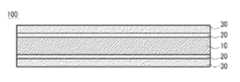
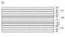
図1乃至図3を参照して第1実施形態について説明する。図1は、ベース基材の概略的な断面図である。図2は、ベース基材上にビルドアップ層を積層した状態を示す概略的な工程図である。図3は、多層プリント配線基板と板状キャリアを剥離する工程を模式的に示す工程図である。<First Embodiment>
The first embodiment will be described with reference to FIGS. 1 to 3. FIG. 1 is a schematic cross-sectional view of a base substrate. FIG. 2 is a schematic process diagram showing a state in which a buildup layer is laminated on a base substrate. FIG. 3 is a process diagram schematically showing a process of peeling the multilayer printed wiring board and the plate-like carrier.
図1に示すようにベース基材100は、所定厚の金属製の板状キャリア10、板状キャリア10の上面(主面)上に積層した離型剤層20、離型剤層20を介して板状キャリア10の上面に積層した樹脂層の一例であるプリプレグ30を備え、板状キャリア10、離型剤層20、及びプリプレグ30がこの順に積層した積層体である。なお、必ずしも板状キャリア10の上面の全面に離型剤層20を成膜する必要はなく、同様に、必ずしも離型剤層20の上面の全面にプリプレグ30を積層する必要はない。板状キャリア10やプリプレグ30の上面視形状は矩形に限らず、円形等の他の形状であっても構わない。プリプレグ30は、典型的には、多層プリント配線基板の最下層を構成するべき層である。換言すれば、プリプレグ30は、ビルドアップ層110を構成する絶縁層40に等しい。この点は、後述の説明からも明らかである。 As shown in FIG. 1, the
ベース基材100の構成層の積層順番に関しては任意であるが、例えば、はじめに板状キャリア10を用意した後、板状キャリア10の上面(主面)上に離型剤層20を積層し、次に、離型剤層20を介してプリプレグ30を積層しても良い。若しくは、プリプレグ30の下面(主面)に離型剤層20を積層し、プリプレグ30と離型剤層20の積層体を板状キャリア10上に積層しても良い。離型剤層20は、通常のコーティング技術を活用してプリプレグ30又は板状キャリア10上に成膜可能である。板状キャリア10若しくはプリプレグ30の厚みは、任意の公知の手段、方法により調整可能である。 Although the order of stacking the constituent layers of the
図2及び図3に示すように、ベース基材100のプリプレグ30上には、1以上の絶縁層40と1以上の配線層50を含むビルドアップ層110が積層される。ビルドアップ層110は、1層の絶縁層40と1層の配線層50の積層体であり、図2においては、プリプレグ30も含めて2層構成のビルドアップ層110が図示されている。ビルドアップ層110の絶縁層40は、好適には樹脂層から成り、より好適には熱硬化性樹脂を含有するプリプレグから成る。ビルドアップ層110の配線層50は、好適にはパターニングされた若しくはパターニングされていない金属層、好適には金属箔若しくはメッキ金属層である。ビルドアップ層110は、絶縁層40と配線層50を順に繰り返し積層することにより形成される。ベース基材100上にビルドアップ層110を積層した後、ベース基材100からビルドアップ層110を分離し、これにより、ビルドアップ層110を好適に薄型の多層プリント配線基板として得ることができる。 As shown in FIGS. 2 and 3, a
このようにして製造される多層プリント配線基板においては、ビルドアップ層110の積層に用いられたベース基材100が含まれない。このような意味において本実施形態に係る多層プリント配線基板が「薄型」構成であると言える。「薄型」であるとは、例えば多層プリント配線基板の厚みが400μm以下、好ましくは200μm以下、より好ましくは100μm以下であることを言う。ただし、多層プリント配線基板の機能上、配線層の層数が極端に多い場合(例えば10層以上)、又は100μmよりも厚い絶縁層又は配線層が必要とされる場合には多層プリント配線基板の厚みが400μmを超える場合があってもよい。 In the multilayer printed wiring board manufactured in this way, the
ビルドアップ層の積層工程においてはベース基材100自体も加熱され、若しくは物理的若しくは化学的に処置され、場合によっては、薬液に浸される。このような工程を経た後においても図3に模式的に示す多層プリント配線基板、端的には多層プリント配線基板の最下層のプリプレグ30と板状キャリア10間の剥離性が確保される。好適には、離型剤層20が板状キャリア10側に残存するが、必ずしもこの限りではない。 In the buildup layer laminating step, the
絶縁層40と配線層50の構成材料や層厚は任意であり、1つの配線層50が、1以上の導電層の積層から構成されても良く、1つの絶縁層40が、1以上の絶縁層の積層から構成されても良い。配線層50は、例えば、1以上の金属箔から構成される。絶縁層40は、1以上の樹脂層から構成され、好適には熱硬化性樹脂層である。配線層50は、必ずしもパターニングされている必要はなく、また、必ずしも他の配線層と電気的に接続されていなくても良い。フローティングの配線層50を設けることは、配線層間に生じる静電容量の制御や多層プリント配線基板の機械的な強度等を調整する際には有効になる場合がある。 The constituent materials and layer thicknesses of the insulating
ビルドアップ層110の具体的な構成は任意である。例えば、ビルドアップ層110は、1以上の絶縁層40と1以上の配線層50を含む。例えば、ビルドアップ層110に含まれる1以上の配線層50が、パターニングされた若しくはパターニングされていない金属箔である。例えば、ビルドアップ層110に含まれる1以上の絶縁層40が、プリプレグである。例えば、ビルドアップ層110が、片面あるいは両面金属張積層板を含む。 The specific configuration of the
板状キャリア10は、金属製、好適には銅又は銅合金製の平板であり、その大きさに依存して多少の可撓性を具備しても良いが、支持基板としての機能を確保できる程度の剛性を具備することが望ましい。板状キャリア10は、典型的には、5μm以上、より好適には10μm以上、30μm以上、35μm以上、50μm以上、65μm以上、70μm以上、80μm以上、100μm以上の厚みを有する金属箔を用いることができる。また、板状キャリア10は典型的には1600μm以下、より好適には1500μm以下、1350μm以下、1000μm以下、800μm以下、500μm以下、400μm以下、300μm以下、105μm以下の厚みを有する金属箔を用いることができる。また、板状キャリア10は、好適には銅箔、又は銅合金箔を使用することができる。 The plate-
板状キャリア10は、一例としては、銅材の圧延により製造された平板であっても良く、銅材が多層に積層されて成る平板であっても良く、この場合、この平板が1600μm以上の厚みを有しても良い。電解により得た銅箔等の銅材を板状キャリア10に活用しても良い。板状キャリア10の構成材料としては銅合金を活用しても構わない。銅合金を活用することにより、板状キャリア10の硬さを高めることができる。銅合金としては、Ni、Si、Zn、Sn、Ti、P、Cr、B、Ag、Mg、Fe、V、Au、Pd、Co、Mn、ベリリウムやカドミウムの元素群から選ばれる一種以上の元素を合計で0質量%以上〜80質量%以下添加した銅合金が例示できる。また、板状キャリア10の材料としては金属であれば特に制限はなく、例えば、銅、金、銀、鉄、ニッケル、アルミニウム、クロム、チタン、亜鉛、マグネシウム等が挙げられる。銅合金、鉄合金等、これらを使用した合金でもよい。 As an example, the plate-
銅としては、典型的には、JIS H0500に規定されるリン脱酸銅、無酸素銅及びタフピッチ銅などの99.90質量%以上の純度の銅が挙げられる。Sn、Ag、Au、Co、Cr、Fe、In、Ni、P、Si、Te、Ti、ZnおよびZrの中の一種以上を合計で0.001〜4.0質量%含有する銅又は銅合金とすることもできる。 Typical examples of copper include copper having a purity of 99.90% by mass or more, such as phosphorus deoxidized copper, oxygen-free copper, and tough pitch copper as defined in JIS H0500. Copper or copper alloy containing 0.001 to 4.0 mass% in total of one or more of Sn, Ag, Au, Co, Cr, Fe, In, Ni, P, Si, Te, Ti, Zn and Zr It can also be.
銅合金としては、更に、チタン銅、リン青銅、コルソン合金、丹銅、黄銅、洋白等が挙げられる。 Examples of the copper alloy further include titanium copper, phosphor bronze, Corson alloy, red brass, brass, and white.
チタン銅は典型的には、Ti:0.5〜5.0質量%を含有し、残部が銅及び不可避的不純物からなる組成を有する。チタン銅は更に、Fe、Co、V、Nb、Mo、B、Ni、P、Zr、Mn、Zn、Si、Mg及びCrの中の1種類以上を合計で2.0質量%以下含有しても良い。 Titanium copper typically contains Ti: 0.5 to 5.0% by mass, with the balance being composed of copper and inevitable impurities. Titanium copper further contains one or more of Fe, Co, V, Nb, Mo, B, Ni, P, Zr, Mn, Zn, Si, Mg, and Cr in total of 2.0% by mass or less. Also good.
リン青銅は典型的には、リン青銅とは銅を主成分としてSn及びこれよりも少ない質量のPを含有する銅合金のことを指す。一例として、りん青銅はSnを3.5〜11質量%、Pを0.03〜0.35質量%含有し、残部銅及び不可避的不純物からなる組成を有する。リン青銅は、Ni、Zn等の元素を合計で1.0質量%以下含有しても良い。 Phosphor bronze typically refers to a copper alloy containing copper as a main component and Sn and a lower mass of P. As an example, phosphor bronze contains Sn in an amount of 3.5 to 11% by mass and P in an amount of 0.03 to 0.35% by mass, and has a composition composed of the remaining copper and inevitable impurities. Phosphor bronze may contain 1.0% by mass or less of elements such as Ni and Zn in total.
コルソン合金は典型的にはSiと化合物を形成する元素(例えば、Ni、Co及びCrの何れか一種以上)が添加され、母相中に第二相粒子として析出する銅合金のことをいう。一例として、コルソン合金はNiを1.0〜4.0質量%、Siを0.2〜1.3質量%含有し、残部銅及び不可避的不純物から構成される組成を有する。別の一例として、コルソン合金はNiを1.0〜4.0質量%、Siを0.2〜1.3質量%、Crを0.03〜0.5質量%含有し、残部銅及び不可避的不純物から構成される組成を有する。更に別の一例として、コルソン合金はNiを1.0〜4.0質量%、Siを0.2〜1.3質量%、Coを0.5〜2.5質量%含有し、残部銅及び不可避的不純物から構成される組成を有する。更に別の一例として、コルソン合金はNiを1.0〜4.0質量%、Siを0.2〜1.3質量%、Coを0.5〜2.5質量%、Crを0.03〜0.5質量%含有し、残部銅及び不可避的不純物から構成される組成を有する。更に別の一例として、コルソン合金はSiを0.2〜1.3質量%、Coを0.5〜2.5質量%含有し、残部銅及び不可避的不純物から構成される組成を有する。コルソン合金には随意にその他の元素(例えば、Mg、Sn、B、Ti、Mn、Ag、P、Zn、As、Sb、Be、Zr、Al及びFe)が添加されてもよい。これらその他の元素は総計で2.0質量%程度まで添加するのが一般的である。例えば、更に別の一例として、コルソン合金はNiを1.0〜4.0質量%、Siを0.2〜1.3質量%、Snを0.01〜2.0質量%、Znを0.01〜2.0質量%含有し、残部銅及び不可避的不純物から構成される組成を有する。 A Corson alloy typically refers to a copper alloy to which an element that forms a compound with Si (for example, any one or more of Ni, Co, and Cr) is added and precipitates as second phase particles in the matrix. As an example, the Corson alloy contains 1.0 to 4.0% by mass of Ni and 0.2 to 1.3% by mass of Si, and has a composition composed of the remaining copper and inevitable impurities. As another example, the Corson alloy contains 1.0 to 4.0% by mass of Ni, 0.2 to 1.3% by mass of Si, 0.03 to 0.5% by mass of Cr, and the balance copper and unavoidable The composition is composed of mechanical impurities. As yet another example, the Corson alloy contains 1.0 to 4.0 mass% Ni, 0.2 to 1.3 mass% Si, 0.5 to 2.5 mass% Co, the balance copper and It has a composition composed of inevitable impurities. As another example, the Corson alloy has a Ni content of 1.0 to 4.0 mass%, a Si content of 0.2 to 1.3 mass%, a Co content of 0.5 to 2.5 mass%, and a Cr content of 0.03. It has a composition composed of ˜0.5% by mass and remaining copper and inevitable impurities. As yet another example, the Corson alloy contains 0.2 to 1.3 mass% of Si and 0.5 to 2.5 mass% of Co, and has a composition composed of the balance copper and unavoidable impurities. Optionally, other elements (eg, Mg, Sn, B, Ti, Mn, Ag, P, Zn, As, Sb, Be, Zr, Al, and Fe) may be added to the Corson alloy. These other elements are generally added up to about 2.0 mass% in total. For example, as yet another example, the Corson alloy has a Ni content of 1.0 to 4.0 mass%, a Si content of 0.2 to 1.3 mass%, a Sn content of 0.01 to 2.0 mass%, and a Zn content of 0. .01-2.0 mass%, and has a composition composed of the remaining copper and unavoidable impurities.
黄銅とは、銅と亜鉛との合金で、特に亜鉛を20質量%以上含有する銅合金のことをいう。亜鉛の上限は特には限定されないが60質量%以下、好ましくは45質量%以下、あるいは40質量%以下である。 Brass is an alloy of copper and zinc, particularly a copper alloy containing 20% by mass or more of zinc. The upper limit of zinc is not particularly limited, but is 60% by mass or less, preferably 45% by mass or less, or 40% by mass or less.
丹銅とは、銅と亜鉛との合金であり亜鉛を1〜20質量%、より好ましくは亜鉛を1〜10質量%含有する銅合金のことをいう。また、丹銅は錫を0.1〜1.0質量%含んでも良い。 The red copper is an alloy of copper and zinc, and means a copper alloy containing 1 to 20% by mass of zinc, more preferably 1 to 10% by mass of zinc. Further, the red copper may contain 0.1 to 1.0% by mass of tin.
洋白とは銅を主成分として、銅を60質量%から75質量%、ニッケルを8.5質量%から19.5質量%、亜鉛を10質量%から30質量%含有する銅合金のことをいう。 Western white is a copper alloy containing copper as a main component, copper from 60% by mass to 75% by mass, nickel from 8.5% by mass to 19.5% by mass, and zinc from 10% by mass to 30% by mass. Say.
アルミニウム及びアルミニウム合金としては、例えばAlを99質量%以上含むものを使用することができる。具体的には、JIS H 4000に記載の合金番号1085、1080、1070、1050、1100、1200、1N00、1N30に代表される、Al:99.00質量%以上のアルミニウム又はその合金等を用いることができる。 As aluminum and aluminum alloy, for example, aluminum containing 99% by mass or more can be used. Specifically, Al: represented by alloy numbers 1085, 1080, 1070, 1050, 1100, 1200, 1N00, and 1N30 described in JIS H 4000, Al: aluminum of 99.00% by mass or more, or an alloy thereof is used. Can do.
ニッケル及びニッケル合金としては、例えばNiを99質量%以上含むものを使用することができる。具体的には、JIS H4551に記載の合金番号NW2200、NW2201に代表される、Ni:99.0質量%以上のニッケル又はその合金等を用いることができる。 As nickel and nickel alloy, for example, nickel containing 99% by mass or more can be used. Specifically, nickel of 99.0% by mass or more represented by alloy numbers NW2200 and NW2201 described in JIS H4551 or an alloy thereof can be used.
鉄合金としては、例えばステンレス、軟鋼、鉄ニッケル合金等を用いることができる。ステンレスは、SUS301、SUS 304、SUS310、SUS 316、SUS 430、SUS 631(いずれもJIS規格)などを用いることができる。軟鋼は、炭素が0.15質量%以下の軟鋼を用いることができ、JIS G3141に記載の軟鋼等を用いることができる。鉄ニッケル合金は、Niを35〜85質量%含み、残部がFe及び不可避不純物からなり、具体的には、JIS C2531に記載の鉄ニッケル合金を用いることができる。また、板状キャリアにはアルミニウム、アルミニウム合金、ニッケル、ニッケル合金、鉄、鉄合金、ステンレスなどの公知の金属も用いることができる。 As the iron alloy, for example, stainless steel, mild steel, iron nickel alloy or the like can be used. SUS301, SUS304, SUS310, SUS316, SUS430, SUS631 (all are JIS standards) etc. can be used for stainless steel. As the mild steel, a mild steel having 0.15% by mass or less of carbon can be used, and a mild steel described in JIS G3141 can be used. The iron-nickel alloy contains 35 to 85% by mass of Ni, and the balance consists of Fe and inevitable impurities. Specifically, an iron-nickel alloy described in JIS C2531 can be used. Moreover, well-known metals, such as aluminum, aluminum alloy, nickel, a nickel alloy, iron, an iron alloy, and stainless steel, can also be used for a plate-shaped carrier.
板状キャリア10のビッカース硬さ(HV)は、典型的には30〜100(F/N)/(d/mm)2であり、好適には50〜80(F/N)/(d/mm)2である。板状キャリア10として銅又は銅合金製の平板の十分な硬さを確保することが望ましい。The Vickers hardness (HV) of the plate-
板状キャリア10に表面処理を施しても構わない。例えば、耐熱性付与を目的とした金属めっき(Niめっき、Ni−Zn合金めっき、Cu−Ni合金めっき、Cu−Zn合金めっき、Znめっき、Cu−Ni−Zn合金めっき、Co−Ni合金めっきなど)、防錆性や耐変色性を付与するためのクロメート処理(クロメート処理液中にZn、P、Ni、Mo、Zr、Ti等の合金元素を1種以上含有させる場合を含む)、表面粗度調整のための粗化処理(例:銅電着粒やCu−Ni−Co合金めっき、Cu−Ni−P合金めっき、Cu−Co合金めっき、Cu−Ni合金めっき、Cu−Co合金めっき、Cu−As合金めっき、Cu−As−W合金めっき等の銅合金めっきによるもの)が挙げられる。粗化処理が板状キャリア10と離型剤層20の剥離強度に影響を与えることはもちろん、クロメート処理も大きな影響を与える。クロメート処理は防錆性や耐変色性の観点から重要であるが、剥離強度を有意に上昇させる傾向が見られるので、剥離強度の調整手段としても意義がある。 The plate-
例えば、銅材の光沢面に対して下記の条件によるニッケル−亜鉛(Ni−Zn)合金めっき処理及びクロメート(Cr−Znクロメート)処理を施しても良い。 For example, the glossy surface of a copper material may be subjected to nickel-zinc (Ni-Zn) alloy plating treatment and chromate (Cr-Zn chromate) treatment under the following conditions.
(ニッケル−亜鉛合金めっき)
Ni濃度 17g/L(NiSO4として添加)
Zn濃度 4g/L(ZnSO4として添加)
pH 3.1
液温 40℃
電流密度 0.1〜10A/dm2
めっき時間 0.1〜10秒(Nickel-zinc alloy plating)
Ni concentration 17g / L (added as NiSO4 )
Zn concentration 4g / L (added as ZnSO4 )
pH 3.1
Current density 0.1-10A / dm2
Plating time 0.1 to 10 seconds
(クロメート処理)
Cr濃度 1.4g/L(CrO3又はK2CrO7として添加)
Zn濃度 0.01〜1.0g/L(ZnSO4として添加)
Na2SO4濃度 10g/L
pH 4.8
液温 55℃
電流密度 0.1〜10A/dm2
めっき時間 0.1〜10秒(Chromate treatment)
Cr concentration 1.4g / L (added as CrO3 or K2 CrO7 )
Zn concentration 0.01 to 1.0 g / L (added as ZnSO4 )
Na2 SO4 concentration 10 g / L
pH 4.8
Liquid temperature 55 ℃
Current density 0.1-10A / dm2
Plating time 0.1 to 10 seconds
離型剤層20は、板状キャリア10に対して相対的に強く固着し、プリプレグ30に対して相対的に弱く固着する任意の材料から選択すると良い。上述のようにビルドアップ層110の積層工程においてベース基材100が加熱され、化学的又は物理的に処理される場合がある。このような観点から、離型剤層20としても耐熱性及び耐薬品性を有し、容易に変質したり薬品により浸食を受けたりしないことが望ましい。離型剤層20は、スピンコーティング、ディップコーティング、スプレーコーティング、印刷等の任意の方法にて板状キャリア10上に形成することができるが、特にこの限りではない。 The
離型剤層20が形成される板状キャリア10の上面は、粗面(M面)又は光沢面(S面)のどちらでも構わないが、粗面よりも光沢面とすることが望ましい。板状キャリアとして圧延金属箔、より好適には圧延銅箔を用いると両面が光沢面となるので、板状キャリアの両面に離型剤層20を形成する場合にはより望ましい。これにより、離型剤層20が積層される板状キャリア10の上面の粗度のバラつきを抑制してベース基材100の品質の安定化を図ることができる。離型剤層20の層厚は、典型的には0.001〜10μmであり、好適には0.001〜0.1μmである。 The upper surface of the plate-
(1)シラン化合物
離型剤層20の構成材料は、本願に開示、若しくは現時点において入手可能なものに限定されるべきものではないが、例えば、次の化学式に示すシラン化合物、その加水分解生成物、該加水分解生成物の縮合体を単独で又は複数組み合わせを離型剤層20に活用すると良い。
当該シラン化合物はアルコキシ基を少なくとも一つ有していることが必要である。アルコキシ基が存在せずに、アルキル基、シクロアルキル基及びアリール基よりなる群から選択される炭化水素基であるか、一つ以上の水素原子がハロゲン原子で置換されたこれら何れかの炭化水素基のみで置換基が構成される場合、離型剤層20と板状キャリア10表面の密着性が低下し過ぎる傾向がある。また、当該シラン化合物はアルキル基、シクロアルキル基及びアリール基よりなる群から選択される炭化水素基であるか、一つ以上の水素原子がハロゲン原子で置換されたこれら何れかの炭化水素基を少なくとも一つ有していることが必要である。当該炭化水素基が存在しない場合、離型剤層20と板状キャリア10表面の密着性が上昇する傾向があるからである。なお、本願発明に係るアルコキシ基には一つ以上の水素原子がハロゲン原子に置換されたアルコキシ基も含まれるものとする。 The silane compound needs to have at least one alkoxy group. A hydrocarbon group selected from the group consisting of an alkyl group, a cycloalkyl group, and an aryl group in the absence of an alkoxy group, or any one of these hydrocarbons in which one or more hydrogen atoms are substituted with a halogen atom When a substituent is comprised only by group, there exists a tendency for the adhesiveness of the mold
板状キャリア10とプリプレグ30(若しくは、プリプレグ30を含むビルドアップ層110)間の剥離強度を後述の好適な範囲に調節する上では、当該シラン化合物はアルコキシ基を三つ、上記炭化水素基(一つ以上の水素原子がハロゲン原子で置換された炭化水素基を含む)を一つ有していることが好ましい。これを上の式でいえば、R3及びR4の両方がアルコキシ基ということになる。In adjusting the peel strength between the plate-
アルコキシ基としては、限定的ではないが、メトキシ基、エトキシ基、n−又はiso−プロポキシ基、n−、iso−又はtert−ブトキシ基、n−、iso−又はneo−ペントキシ基、n−ヘキソキシ基、シクロヘキシソキシ基、n−ヘプトキシ基、及びn−オクトキシ基等の直鎖状、分岐状、又は環状の炭素数1〜20、好ましくは炭素数1〜10、より好ましくは炭素数1〜5のアルコキシ基が挙げられる。ハロゲン原子としては、フッ素原子、塩素原子、臭素原子及びヨウ素原子が挙げられる。 Examples of the alkoxy group include, but are not limited to, methoxy group, ethoxy group, n- or iso-propoxy group, n-, iso- or tert-butoxy group, n-, iso- or neo-pentoxy group, n-hexoxy. Group, cyclohexyloxy group, n-heptoxy group, n-octoxy group, etc., linear, branched, or cyclic carbon number of 1 to 20, preferably 1 to 10, more preferably 1 to 5 alkoxy groups. Examples of the halogen atom include a fluorine atom, a chlorine atom, a bromine atom, and an iodine atom.
アルキル基としては、限定的ではないが、メチル基、エチル基、n−又はiso−プロピル基、n−、iso−又はtert−ブチル基、n−、iso−又はneo−ペンチル基、n−ヘキシル基、n−オクチル基、n−デシル基等の直鎖状又は分岐状の炭素数1〜20、好ましくは炭素数1〜10、より好ましくは炭素数1〜5のアルキル基が挙げられる。 Examples of the alkyl group include, but are not limited to, methyl group, ethyl group, n- or iso-propyl group, n-, iso- or tert-butyl group, n-, iso- or neo-pentyl group, and n-hexyl. A linear or branched alkyl group having 1 to 20, preferably 1 to 10 carbon atoms, more preferably 1 to 5 carbon atoms, such as a group, an n-octyl group, and an n-decyl group.
シクロアルキル基としては、限定的ではないが、シクロプロピル基、シクロブチル基、シクロペンチル基、シクロヘキシル基、シクロへプチル基、シクロオクチル基等の炭素数3〜10、好ましくは炭素数5〜7のシクロアルキル基が挙げられる。 Examples of the cycloalkyl group include, but are not limited to, cyclopropyl groups, cyclobutyl groups, cyclopentyl groups, cyclohexyl groups, cycloheptyl groups, cyclooctyl groups, and the like. An alkyl group is mentioned.
アリール基としては、フェニル基、アルキル基で置換されたフェニル基(例:トリル基、キシリル基)、1−又は2−ナフチル基、アントリル基等の炭素数6〜20、好ましくは6〜14のアリール基が挙げられる。 As the aryl group, a phenyl group substituted with an alkyl group (eg, tolyl group, xylyl group), 1- or 2-naphthyl group, anthryl group, etc., having 6 to 20, preferably 6 to 14 carbon atoms. An aryl group is mentioned.
これらの炭化水素基は一つ以上の水素原子がハロゲン原子で置換されてもよく、例えば、フッ素原子、塩素原子、又は臭素原子で置換されることができる。 In these hydrocarbon groups, one or more hydrogen atoms may be substituted with a halogen atom, and may be substituted with, for example, a fluorine atom, a chlorine atom, or a bromine atom.
好ましいシラン化合物の例としては、メチルトリメトキシシラン、エチルトリメトキシシラン、n−又はiso−プロピルトリメトキシシラン、n−、iso−又はtert−ブチルトリメトキシシラン、n−、iso−又はneo−ペンチルトリメトキシシラン、ヘキシルトリメトキシシラン、オクチルトリメトキシシラン、デシルトリメトキシシラン、フェニルトリメトキシシラン;アルキル置換フェニルトリメトキシシラン(例えば、p−(メチル)フェニルトリメトキシシラン)、メチルトリエトキシシラン、エチルトリエトキシシラン、n−又はiso−プロピルトリエトキシシラン、n−、iso−又はtert−ブチルトリエトキシシラン、ペンチルトリエトキシシラン、ヘキシルトリエトキシシラン、オクチルトリエトキシシラン、デシルトリエトキシシラン、フェニルトリエトキシシラン、アルキル置換フェニルトリエトキシシラン(例えば、p−(メチル)フェニルトリエトキシシラン)、(3,3,3−トリフルオロプロピル)トリメトキシシラン、及びトリデカフルオロオクチルトリエトキシシラン、メチルトリクロロシラン、ジメチルジクロロシラン、トリメチルクロロシラン、フェニルトリクロロシラン、トリメチルフルオロシラン、ジメチルジブロモシラン、ジフェニルジブロモシラン、これらの加水分解生成物、及びこれらの加水分解生成物の縮合体などが挙げられる。これらの中でも、入手の容易性の観点から、プロピルトリメトキシシラン、メチルトリエトキシシラン、ヘキシルトリメトキシシラン、フェニルトリエトキシシラン、デシルトリメトキシシランが好ましい。 Examples of preferred silane compounds include methyltrimethoxysilane, ethyltrimethoxysilane, n- or iso-propyltrimethoxysilane, n-, iso- or tert-butyltrimethoxysilane, n-, iso- or neo-pentyl. Trimethoxysilane, hexyltrimethoxysilane, octyltrimethoxysilane, decyltrimethoxysilane, phenyltrimethoxysilane; alkyl-substituted phenyltrimethoxysilane (eg, p- (methyl) phenyltrimethoxysilane), methyltriethoxysilane, ethyl Triethoxysilane, n- or iso-propyltriethoxysilane, n-, iso- or tert-butyltriethoxysilane, pentyltriethoxysilane, hexyltriethoxysilane, octyltriethoxy Lan, decyltriethoxysilane, phenyltriethoxysilane, alkyl-substituted phenyltriethoxysilane (eg, p- (methyl) phenyltriethoxysilane), (3,3,3-trifluoropropyl) trimethoxysilane, and trideca Fluorooctyltriethoxysilane, methyltrichlorosilane, dimethyldichlorosilane, trimethylchlorosilane, phenyltrichlorosilane, trimethylfluorosilane, dimethyldibromosilane, diphenyldibromosilane, their hydrolysis products, and condensates of these hydrolysis products Etc. Among these, propyltrimethoxysilane, methyltriethoxysilane, hexyltrimethoxysilane, phenyltriethoxysilane, and decyltrimethoxysilane are preferable from the viewpoint of availability.
(2)分子内に2つ以下のメルカプト基を有する化合物
上述のシラン化合物に代えて、分子内に2つ以下のメルカプト基を有する化合物を離型剤層20に活用しても良い。この例としては、チオール、ジチオール、チオカルボン酸又はその塩、ジチオカルボン酸又はその塩、チオスルホン酸又はその塩、及びジチオスルホン酸又はその塩が挙げられ、これらの中から選択される少なくとも一種を用いることができる。(2) Compound having two or less mercapto groups in the molecule Instead of the above-mentioned silane compound, a compound having two or less mercapto groups in the molecule may be used for the
チオールは、分子内に一つのメルカプト基を有するものであり、例えばR−SHで表される。ここで、Rは、水酸基又はアミノ基を含んでもよい、脂肪族系又は芳香族系炭化水素基又は複素環基を表す。 The thiol has one mercapto group in the molecule and is represented by R-SH, for example. Here, R represents an aliphatic or aromatic hydrocarbon group or heterocyclic group which may contain a hydroxyl group or an amino group.
ジチオールは、分子内に二つのメルカプト基を有するものであり、例えばR(SH)2で表される。Rは、水酸基又はアミノ基を含んでもよい、脂肪族系又は芳香族系炭化水素基又は複素環基を表す。また、二つのメルカプト基は、それぞれ同じ炭素に結合してもよいし、互いに別々の炭素又は窒素に結合してもよい。Dithiol has two mercapto groups in the molecule and is represented by, for example, R (SH)2 . R represents an aliphatic or aromatic hydrocarbon group or heterocyclic group which may contain a hydroxyl group or an amino group. Two mercapto groups may be bonded to the same carbon, or may be bonded to different carbons or nitrogens.
チオカルボン酸は、有機カルボン酸の水酸基がメルカプト基に置換されたものであり、例えばR−CO−SHで表される。Rは、水酸基又はアミノ基を含んでもよい、脂肪族系又は芳香族系炭化水素基又は複素環基を表す。また、チオカルボン酸は、塩の形態でも使用することが可能である。なお、チオカルボン酸基を、二つ有する化合物も使用可能である。 A thiocarboxylic acid is one in which a hydroxyl group of an organic carboxylic acid is substituted with a mercapto group, and is represented by R-CO-SH, for example. R represents an aliphatic or aromatic hydrocarbon group or heterocyclic group which may contain a hydroxyl group or an amino group. The thiocarboxylic acid can also be used in the form of a salt. A compound having two thiocarboxylic acid groups can also be used.
ジチオカルボン酸は、有機カルボン酸のカルボキシ基中の2つの酸素原子が硫黄原子に置換されたものであり、例えばR−(CS)−SHで表される。Rは、水酸基又はアミノ基を含んでもよい、脂肪族系又は芳香族系炭化水素基又は複素環基を表す。また、ジチオカルボン酸は、塩の形態でも使用することが可能である。なお、ジチオカルボン酸基を、二つ有する化合物も使用可能である。 The dithiocarboxylic acid is one in which two oxygen atoms in the carboxy group of the organic carboxylic acid are substituted with sulfur atoms, and is represented by, for example, R- (CS) -SH. R represents an aliphatic or aromatic hydrocarbon group or heterocyclic group which may contain a hydroxyl group or an amino group. Dithiocarboxylic acid can also be used in the form of a salt. A compound having two dithiocarboxylic acid groups can also be used.
チオスルホン酸は、有機スルホン酸の水酸基がメルカプト基に置換されたものであり、例えばR(SO2)−SHで表される。Rは、水酸基又はアミノ基を含んでもよい、脂肪族系又は芳香族系炭化水素基又は複素環基を表す。また、チオスルホン酸は、塩の形態でも使用することが可能である。The thiosulfonic acid is obtained by replacing the hydroxyl group of an organic sulfonic acid with a mercapto group, and is represented by, for example, R (SO2 ) —SH. R represents an aliphatic or aromatic hydrocarbon group or heterocyclic group which may contain a hydroxyl group or an amino group. Further, thiosulfonic acid can be used in the form of a salt.
ジチオスルホン酸は、有機ジスルホン酸の二つの水酸基がそれぞれメルカプト基に置換されたものであり、例えばR−((SO2)−SH)2で表される。Rは、水酸基又はアミノ基を含んでもよい、脂肪族系又は芳香族系炭化水素基又は複素環基を表す。また、二つのチオスルホン酸基は、それぞれ同じ炭素に結合してもよいし、互いに別々の炭素に結合してもよい。また、ジチオスルホン酸は、塩の形態でも使用することが可能である。Dithiosulfonic acid is one in which two hydroxyl groups of an organic disulfonic acid are each substituted with a mercapto group, and is represented by, for example, R-((SO2 ) -SH)2 . R represents an aliphatic or aromatic hydrocarbon group or heterocyclic group which may contain a hydroxyl group or an amino group. Two thiosulfonic acid groups may be bonded to the same carbon, or may be bonded to different carbons. Dithiosulfonic acid can also be used in the form of a salt.
ここで、Rとして好適な脂肪族系炭化水素基としては、アルキル基、シクロアルキル基が挙げられ、これら炭化水素基は水酸基とアミノ基のどちらか又は両方を含んでいてもよい。 Here, examples of the aliphatic hydrocarbon group suitable as R include an alkyl group and a cycloalkyl group, and these hydrocarbon groups may contain either or both of a hydroxyl group and an amino group.
また、アルキル基としては、限定的ではないが、メチル基、エチル基、n−又はiso−プロピル基、n−、iso−又はtert−ブチル基、n−、iso−又はneo−ペンチル基、n−ヘキシル基、n−オクチル基、n−デシル基等の直鎖状又は分岐状の炭素数1〜20、好ましくは炭素数1〜10、より好ましくは炭素数1〜5のアルキル基が挙げられる。 Examples of the alkyl group include, but are not limited to, methyl group, ethyl group, n- or iso-propyl group, n-, iso- or tert-butyl group, n-, iso- or neo-pentyl group, n -A linear or branched alkyl group having 1 to 20, preferably 1 to 10, more preferably 1 to 5 carbon atoms, such as a hexyl group, an n-octyl group, and an n-decyl group. .
また、シクロアルキル基としては、限定的ではないが、シクロプロピル基、シクロブチル基、シクロペンチル基、シクロヘキシル基、シクロへプチル基、シクロオクチル基等の炭素数3〜10、好ましくは炭素数5〜7のシクロアルキル基が挙げられる。 Moreover, as a cycloalkyl group, although it is not limited, C3-C10, such as a cyclopropyl group, a cyclobutyl group, a cyclopentyl group, a cyclohexyl group, a cycloheptyl group, a cyclooctyl group, Preferably it is C5-C7 Of the cycloalkyl group.
また、Rとして好適な芳香族炭化水素基としては、フェニル基、アルキル基で置換されたフェニル基(例:トリル基、キシリル基)、1−又は2−ナフチル基、アントリル基等の炭素数6〜20、好ましくは6〜14のアリール基が挙げられ、これら炭化水素基は水酸基とアミノ基のどちらか又は両方を含んでいてもよい。 Further, examples of the aromatic hydrocarbon group suitable as R include a phenyl group, a phenyl group substituted with an alkyl group (eg, tolyl group, xylyl group), 1- or 2-naphthyl group, anthryl group and the like. -20, preferably 6-14 aryl groups are mentioned, and these hydrocarbon groups may contain either or both of a hydroxyl group and an amino group.
また、Rとして好適な複素環基としては、イミダゾール、トリアゾール、テトラゾール、ベンゾイミダゾール、ベンゾトリアゾール、チアゾール、ベンゾチアゾールが挙げられ、水酸基とアミノ基のどちらか又は両方を含んでいてもよい。 Moreover, examples of the heterocyclic group suitable as R include imidazole, triazole, tetrazole, benzimidazole, benzotriazole, thiazole, and benzothiazole, which may contain either or both of a hydroxyl group and an amino group.
分子内に2つ以下のメルカプト基を有する化合物の好ましい例としては、3−メルカプト−1,2プロパンジオール、2−メルカプトエタノール、1,2−エタンジチオール、6−メルカプト−1−ヘキサノール、1−オクタンチオール、1−ドデカンチオール、10−ヒドロキシ−1−ドデカンチオール、10−カルボキシ−1−ドデカンチオール、10−アミノ−1−ドデカンチオール、1−ドデカンチオールスルホン酸ナトリウム、チオフェノール、チオ安息香酸、4−アミノ−チオフェノール、p−トルエンチオール、2,4−ジメチルベンゼンチオール、3−メルカプト−1,2,4トリアゾール、2−メルカプト−ベンゾチアゾールが挙げられる。これらの中でも水溶性と廃棄物処理上の観点から、3−メルカプト−1,2プロパンジオールが好ましい。 Preferred examples of the compound having 2 or less mercapto groups in the molecule include 3-mercapto-1,2propanediol, 2-mercaptoethanol, 1,2-ethanedithiol, 6-mercapto-1-hexanol, 1- Octanethiol, 1-dodecanethiol, 10-hydroxy-1-dodecanethiol, 10-carboxy-1-dodecanethiol, 10-amino-1-dodecanethiol, sodium 1-dodecanethiolsulfonate, thiophenol, thiobenzoic acid, Examples include 4-amino-thiophenol, p-toluenethiol, 2,4-dimethylbenzenethiol, 3-mercapto-1,2,4 triazole, and 2-mercapto-benzothiazole. Among these, 3-mercapto-1,2 propanediol is preferable from the viewpoint of water solubility and waste disposal.
(3)金属アルコキシド
次式に示す構造を有するアルミネート化合物、チタネート化合物、ジルコネート化合物、又はその加水分解生成物質、又は該加水分解生成物質の縮合体(以下、単に金属アルコキシドと記述する)を単独で又は複数混合して使用して、板状キャリア10とプリプレグ30を貼り合わせることで、適度に密着性が低下し、剥離強度を後述するような範囲に調節できる。(3) Metal alkoxide An aluminate compound, titanate compound, zirconate compound having a structure represented by the following formula, or a hydrolysis product thereof, or a condensate of the hydrolysis product (hereinafter simply referred to as a metal alkoxide) alone Or by mixing and using the plate-
式中、R1はアルコキシ基又はハロゲン原子であり、R2はアルキル基、シクロアルキル基及びアリール基よりなる群から選択される炭化水素基であるか、一つ以上の水素原子がハロゲン原子で置換されたこれら何れかの炭化水素基であり、MはAl、Ti、Zrのうちいずれか一つ、nは0又は1又は2、mは1以上Mの価数以下の整数であり、R1の少なくとも一つはアルコキシ基である。なお、m+nはMの価数すなわちAlの場合3、Ti、Zrの場合4である。In the formula, R1 is an alkoxy group or a halogen atom, and R2 is a hydrocarbon group selected from the group consisting of an alkyl group, a cycloalkyl group and an aryl group, or one or more hydrogen atoms are halogen atoms. Any one of these substituted hydrocarbon groups, M is any one of Al, Ti, and Zr, n is 0, 1 or 2, m is an integer from 1 to M, and RAt least one of1 is an alkoxy group. M + n is the valence of M, that is, 3 for Al and 4 for Ti and Zr.
当該金属アルコキシドはアルコキシ基を少なくとも一つ有していることが必要である。アルコキシ基が存在せずに、アルキル基、シクロアルキル基及びアリール基よりなる群から選択される炭化水素基であるか、一つ以上の水素原子がハロゲン原子で置換されたこれら何れかの炭化水素基のみで置換基が構成される場合、板状キャリアと金属箔表面の密着性が低下し過ぎる傾向がある。また、当該金属アルコキシドはアルキル基、シクロアルキル基及びアリール基よりなる群から選択される炭化水素基であるか、一つ以上の水素原子がハロゲン原子で置換されたこれら何れかの炭化水素基を0〜2個有していることが必要である。当該炭化水素基を3つ以上有する場合、板状キャリアと金属箔表面の密着性が低下し過ぎる傾向があるからである。なお、本願発明に係るアルコキシ基には一つ以上の水素原子がハロゲン原子に置換されたアルコキシ基も含まれるものとする。板状キャリア10とプリプレグ30(若しくは、プリプレグ30を含むビルドアップ層110)の剥離強度を後述の範囲に調節する上では、当該金属アルコキシドはアルコキシ基を二つ以上、上記炭化水素基(一つ以上の水素原子がハロゲン原子で置換された炭化水素基を含む)を一つか二つ有していることが好ましい。 The metal alkoxide needs to have at least one alkoxy group. A hydrocarbon group selected from the group consisting of an alkyl group, a cycloalkyl group, and an aryl group in the absence of an alkoxy group, or any one of these hydrocarbons in which one or more hydrogen atoms are substituted with a halogen atom When a substituent is comprised only by group, there exists a tendency for the adhesiveness of a plate-shaped carrier and metal foil surface to fall too much. The metal alkoxide is a hydrocarbon group selected from the group consisting of an alkyl group, a cycloalkyl group, and an aryl group, or any one of these hydrocarbon groups in which one or more hydrogen atoms are substituted with a halogen atom. It is necessary to have 0 to 2 pieces. This is because when three or more hydrocarbon groups are present, the adhesion between the plate-like carrier and the metal foil surface tends to be excessively lowered. The alkoxy group according to the present invention includes an alkoxy group in which one or more hydrogen atoms are substituted with halogen atoms. In adjusting the peel strength between the plate-
また、アルキル基としては、限定的ではないが、メチル基、エチル基、n−又はiso−プロピル基、n−、iso−又はtert−ブチル基、n−、iso−又はneo−ペンチル基、n−ヘキシル基、n−オクチル基、n−デシル基等の直鎖状又は分岐状の炭素数1〜20、好ましくは炭素数1〜10、より好ましくは炭素数1〜5のアルキル基が挙げられる。 Examples of the alkyl group include, but are not limited to, methyl group, ethyl group, n- or iso-propyl group, n-, iso- or tert-butyl group, n-, iso- or neo-pentyl group, n -A linear or branched alkyl group having 1 to 20, preferably 1 to 10, more preferably 1 to 5 carbon atoms, such as a hexyl group, an n-octyl group, and an n-decyl group. .
また、シクロアルキル基としては、限定的ではないが、シクロプロピル基、シクロブチル基、シクロペンチル基、シクロヘキシル基、シクロへプチル基、シクロオクチル基等の炭素数3〜10、好ましくは炭素数5〜7のシクロアルキル基が挙げられる。 Moreover, as a cycloalkyl group, although it is not limited, C3-C10, such as a cyclopropyl group, a cyclobutyl group, a cyclopentyl group, a cyclohexyl group, a cycloheptyl group, a cyclooctyl group, Preferably it is C5-C7 Of the cycloalkyl group.
また、R2として好適な芳香族炭化水素基としては、フェニル基、アルキル基で置換されたフェニル基(例:トリル基、キシリル基)、1−又は2−ナフチル基、アントリル基等の炭素数6〜20、好ましくは6〜14のアリール基が挙げられ、これら炭化水素基は水酸基とアミノ基のどちらか又は両方を含んでいてもよい。
これらの炭化水素基は一つ以上の水素原子がハロゲン原子で置換されてもよく、例えば、フッ素原子、塩素原子、又は臭素原子で置換されることができる。In addition, examples of the aromatic hydrocarbon group suitable as R2 include a phenyl group, a phenyl group substituted with an alkyl group (eg, tolyl group, xylyl group), 1- or 2-naphthyl group, anthryl group, and the like. Examples of the aryl group include 6 to 20, preferably 6 to 14, and these hydrocarbon groups may contain one or both of a hydroxyl group and an amino group.
In these hydrocarbon groups, one or more hydrogen atoms may be substituted with a halogen atom, and may be substituted with, for example, a fluorine atom, a chlorine atom, or a bromine atom.
好ましいアルミネート化合物の例としては、トリメトキシアルミニウム、メチルジメトキシアルミニウム、エチルジメトキシアルミニウム、n−又はiso−プロピルジメトキシアルミニウム、n−、iso−又はtert−ブチルジメトキシアルミニウム、n−、iso−又はneo−ペンチルジメトキシアルミニウム、ヘキシルジメトキシアルミニウム、オクチルジメトキシアルミニウム、デシルジメトキシアルミニウム、フェニルジメトキシアルミニウム;アルキル置換フェニルジメトキシアルミニウム(例えば、p−(メチル)フェニルジメトキシアルミニウム)、ジメチルメトキシアルミニウム、トリエトキシアルミニウム、メチルジエトキシアルミニウム、エチルジエトキシアルミニウム、n−又はiso−プロピルジエトキシアルミニウム、n−、iso−又はtert−ブチルジエトキシアルミニウム、ペンチルジエトキシアルミニウム、ヘキシルジエトキシアルミニウム、オクチルジエトキシアルミニウム、デシルジエトキシアルミニウム、フェニルジエトキシアルミニウム、アルキル置換フェニルジエトキシアルミニウム(例えば、p−(メチル)フェニルジエトキシアルミニウム)、ジメチルエトキシアルミニウム、トリイソプロポキシアルミニウム、メチルジイソプロポキシアルミニウム、エチルジイソプロポキシアルミニウム、n−又はiso−プロピルジエトキシアルミニウム、n−、iso−又はtert−ブチルジイソプロポキシアルミニウム、ペンチルジイソプロポキシアルミニウム、ヘキシルジイソプロポキシアルミニウム、オクチルジイソプロポキシアルミニウム、デシルジイソプロポキシアルミニウム、フェニルジイソプロポキシアルミニウム、アルキル置換フェニルジイソプロポキシアルミニウム(例えば、p−(メチル)フェニルジイソプロポキシアルミニウム)、ジメチルイソプロポキシアルミニウム、(3,3,3−トリフルオロプロピル)ジメトキシアルミニウム、及びトリデカフルオロオクチルジエトキシアルミニウム、メチルジクロロアルミニウム、ジメチルクロロアルミニウム、ジメチルクロロアルミニウム、フェニルジクロロアルミニウム、ジメチルフルオロアルミニウム、ジメチルブロモアルミニウム、ジフェニルブロモアルミニウム、これらの加水分解生成物、及びこれらの加水分解生成物の縮合体などが挙げられる。これらの中でも、入手の容易性の観点から、トリメトキシアルミニウム、トリエトキシアルミニウム、トリイソプロポキシアルミニウム、が好ましい。 Examples of preferred aluminate compounds include trimethoxyaluminum, methyldimethoxyaluminum, ethyldimethoxyaluminum, n- or iso-propyldimethoxyaluminum, n-, iso- or tert-butyldimethoxyaluminum, n-, iso- or neo- Pentyl dimethoxy aluminum, hexyl dimethoxy aluminum, octyl dimethoxy aluminum, decyl dimethoxy aluminum, phenyl dimethoxy aluminum; alkyl-substituted phenyl dimethoxy aluminum (for example, p- (methyl) phenyl dimethoxy aluminum), dimethyl methoxy aluminum, triethoxy aluminum, methyl diethoxy aluminum Ethyldiethoxyaluminum, n- or iso-propyldiethoxy Luminium, n-, iso- or tert-butyldiethoxyaluminum, pentyldiethoxyaluminum, hexyldiethoxyaluminum, octyldiethoxyaluminum, decyldiethoxyaluminum, phenyldiethoxyaluminum, alkyl-substituted phenyldiethoxyaluminum (eg p -(Methyl) phenyldiethoxyaluminum), dimethylethoxyaluminum, triisopropoxyaluminum, methyldiisopropoxyaluminum, ethyldiisopropoxyaluminum, n- or iso-propyldiethoxyaluminum, n-, iso- or tert-butyl Diisopropoxy aluminum, pentyl diisopropoxy aluminum, hexyl diisopropoxy aluminum, octyl diiso Ropoxyaluminum, decyldiisopropoxyaluminum, phenyldiisopropoxyaluminum, alkyl-substituted phenyldiisopropoxyaluminum (eg, p- (methyl) phenyldiisopropoxyaluminum), dimethylisopropoxyaluminum, (3,3,3- Trifluoropropyl) dimethoxyaluminum, and tridecafluorooctyldiethoxyaluminum, methyldichloroaluminum, dimethylchloroaluminum, dimethylchloroaluminum, phenyldichloroaluminum, dimethylfluoroaluminum, dimethylbromoaluminum, diphenylbromoaluminum, and their hydrolysis products And condensates of these hydrolysis products. Among these, from the viewpoint of availability, trimethoxyaluminum, triethoxyaluminum, and triisopropoxyaluminum are preferable.
好ましいチタネート化合物の例としては、テトラメトキシチタン、メチルトリメトキシチタン、エチルトリメトキシチタン、n−又はiso−プロピルトリメトキシチタン、n−、iso−又はtert−ブチルトリメトキシチタン、n−、iso−又はneo−ペンチルトリメトキシチタン、ヘキシルトリメトキシチタン、オクチルトリメトキシチタン、デシルトリメトキシチタン、フェニルトリメトキシチタン;アルキル置換フェニルトリメトキシチタン(例えば、p−(メチル)フェニルトリメトキシチタン)、ジメチルジメトキシチタン、テトラエトキシチタン、メチルトリエトキシチタン、エチルトリエトキシチタン、n−又はiso−プロピルトリエトキシチタン、n−、iso−又はtert−ブチルトリエトキシチタン、ペンチルトリエトキシチタン、ヘキシルトリエトキシチタン、オクチルトリエトキシチタン、デシルトリエトキシチタン、フェニルトリエトキシチタン、アルキル置換フェニルトリエトキシチタン(例えば、p−(メチル)フェニルトリエトキシチタン)、ジメチルジエトキシチタン、テトライソプロポキシチタン、メチルトリイソプロポキシチタン、エチルトリイソプロポキシチタン、n−又はiso−プロピルトリエトキシチタン、n−、iso−又はtert−ブチルトリイソプロポキシチタン、ペンチルトリイソプロポキシチタン、ヘキシルトリイソプロポキシチタン、オクチルトリイソプロポキシチタン、デシルトリイソプロポキシチタン、フェニルトリイソプロポキシチタン、アルキル置換フェニルトリイソプロポキシチタン(例えば、p−(メチル)フェニルトリイソプロポキシチタン)、ジメチルジイソプロポキシチタン、(3,3,3−トリフルオロプロピル)トリメトキシチタン、及びトリデカフルオロオクチルトリエトキシチタン、メチルトリクロロチタン、ジメチルジクロロチタン、トリメチルクロロチタン、フェニルトリクロロチタン、ジメチルジフルオロチタン、ジメチルジブロモチタン、ジフェニルジブロモチタン、これらの加水分解生成物、及びこれらの加水分解生成物の縮合体などが挙げられる。これらの中でも、入手の容易性の観点から、テトラメトキシチタン、テトラエトキシチタン、テトライソプロポキシチタン、が好ましい。 Examples of preferred titanate compounds include tetramethoxy titanium, methyl trimethoxy titanium, ethyl trimethoxy titanium, n- or iso-propyl trimethoxy titanium, n-, iso- or tert-butyl trimethoxy titanium, n-, iso- Or neo-pentyltrimethoxytitanium, hexyltrimethoxytitanium, octyltrimethoxytitanium, decyltrimethoxytitanium, phenyltrimethoxytitanium; alkyl-substituted phenyltrimethoxytitanium (eg, p- (methyl) phenyltrimethoxytitanium), dimethyldimethoxy Titanium, tetraethoxy titanium, methyl triethoxy titanium, ethyl triethoxy titanium, n- or iso-propyl triethoxy titanium, n-, iso- or tert-butyl triethoxy titanium, Tiltlyethoxytitanium, Hexyltriethoxytitanium, Octyltriethoxytitanium, Decyltriethoxytitanium, Phenyltriethoxytitanium, Alkyl-substituted phenyltriethoxytitanium (eg, p- (methyl) phenyltriethoxytitanium), Dimethyldiethoxytitanium, Tetraisopropoxytitanium, methyltriisopropoxytitanium, ethyltriisopropoxytitanium, n- or iso-propyltriethoxytitanium, n-, iso- or tert-butyltriisopropoxytitanium, pentyltriisopropoxytitanium, hexyltriiso Propoxy titanium, octyltriisopropoxy titanium, decyl triisopropoxy titanium, phenyl triisopropoxy titanium, alkyl substituted phenyl triisopropoxy titanium (example P- (methyl) phenyltriisopropoxytitanium), dimethyldiisopropoxytitanium, (3,3,3-trifluoropropyl) trimethoxytitanium, and tridecafluorooctyltriethoxytitanium, methyltrichlorotitanium, dimethyldichloro Examples include titanium, trimethylchlorotitanium, phenyltrichlorotitanium, dimethyldifluorotitanium, dimethyldibromotitanium, diphenyldibromotitanium, hydrolysis products thereof, and condensates of these hydrolysis products. Among these, tetramethoxy titanium, tetraethoxy titanium, and tetraisopropoxy titanium are preferable from the viewpoint of availability.
好ましいジルコネート化合物の例としては、テトラメトキシジルコニウム、メチルトリメトキシジルコニウム、エチルトリメトキシジルコニウム、n−又はiso−プロピルトリメトキシジルコニウム、n−、iso−又はtert−ブチルトリメトキシジルコニウム、n−、iso−又はneo−ペンチルトリメトキシジルコニウム、ヘキシルトリメトキシジルコニウム、オクチルトリメトキシジルコニウム、デシルトリメトキシジルコニウム、フェニルトリメトキシジルコニウム;アルキル置換フェニルトリメトキシジルコニウム(例えば、p−(メチル)フェニルトリメトキシジルコニウム)、ジメチルジメトキシジルコニウム、テトラエトキシジルコニウム、メチルトリエトキシジルコニウム、エチルトリエトキシジルコニウム、n−又はiso−プロピルトリエトキシジルコニウム、n−、iso−又はtert−ブチルトリエトキシジルコニウム、ペンチルトリエトキシジルコニウム、ヘキシルトリエトキシジルコニウム、オクチルトリエトキシジルコニウム、デシルトリエトキシジルコニウム、フェニルトリエトキシジルコニウム、アルキル置換フェニルトリエトキシジルコニウム(例えば、p−(メチル)フェニルトリエトキシジルコニウム)、ジメチルジエトキシジルコニウム、テトライソプロポキシジルコニウム、メチルトリイソプロポキシジルコニウム、エチルトリイソプロポキシジルコニウム、n−又はiso−プロピルトリエトキシジルコニウム、n−、iso−又はtert−ブチルトリイソプロポキシジルコニウム、ペンチルトリイソプロポキシジルコニウム、ヘキシルトリイソプロポキシジルコニウム、オクチルトリイソプロポキシジルコニウム、デシルトリイソプロポキシジルコニウム、フェニルトリイソプロポキシジルコニウム、アルキル置換フェニルトリイソプロポキシジルコニウム(例えば、p−(メチル)フェニルトリイソプロポキシチタン)、ジメチルジイソプロポキシジルコニウム、(3,3,3−トリフルオロプロピル)トリメトキシジルコニウム、及びトリデカフルオロオクチルトリエトキシジルコニウム、メチルトリクロロジルコニウム、ジメチルジクロロジルコニウム、トリメチルクロロジルコニウム、フェニルトリクロロジルコニウム、ジメチルジフルオロジルコニウム、ジメチルジブロモジルコニウム、ジフェニルジブロモジルコニウム、これらの加水分解生成物、及びこれらの加水分解生成物の縮合体などが挙げられる。これらの中でも、入手の容易性の観点から、テトラメトキシジルコニウム、テトラエトキシジルコニウム、テトライソプロポキシジルコニウム、が好ましい。 Examples of preferred zirconate compounds include tetramethoxyzirconium, methyltrimethoxyzirconium, ethyltrimethoxyzirconium, n- or iso-propyltrimethoxyzirconium, n-, iso- or tert-butyltrimethoxyzirconium, n-, iso- Or neo-pentyltrimethoxyzirconium, hexyltrimethoxyzirconium, octyltrimethoxyzirconium, decyltrimethoxyzirconium, phenyltrimethoxyzirconium; alkyl-substituted phenyltrimethoxyzirconium (eg, p- (methyl) phenyltrimethoxyzirconium), dimethyldimethoxy Zirconium, tetraethoxyzirconium, methyltriethoxyzirconium, ethyltriethoxyzirconium, n Or iso-propyltriethoxyzirconium, n-, iso- or tert-butyltriethoxyzirconium, pentyltriethoxyzirconium, hexyltriethoxyzirconium, octyltriethoxyzirconium, decyltriethoxyzirconium, phenyltriethoxyzirconium, alkyl-substituted phenyltri Ethoxyzirconium (eg, p- (methyl) phenyltriethoxyzirconium), dimethyldiethoxyzirconium, tetraisopropoxyzirconium, methyltriisopropoxyzirconium, ethyltriisopropoxyzirconium, n- or iso-propyltriethoxyzirconium, n- , Iso- or tert-butyltriisopropoxyzirconium, pentyltriisopropoxydi Konium, hexyltriisopropoxyzirconium, octyltriisopropoxyzirconium, decyltriisopropoxyzirconium, phenyltriisopropoxyzirconium, alkyl-substituted phenyltriisopropoxyzirconium (eg, p- (methyl) phenyltriisopropoxytitanium), dimethyldi Isopropoxyzirconium, (3,3,3-trifluoropropyl) trimethoxyzirconium, and tridecafluorooctyltriethoxyzirconium, methyltrichlorozirconium, dimethyldichlorozirconium, trimethylchlorozirconium, phenyltrichlorozirconium, dimethyldifluorozirconium, dimethyldibromo Zirconium, diphenyldibromozirconium and their hydrolyzed products Examples thereof include condensates of these products and hydrolysis products thereof. Among these, tetramethoxyzirconium, tetraethoxyzirconium, and tetraisopropoxyzirconium are preferable from the viewpoint of availability.
ベース基材100は、板状キャリア10とプリプレグ30をホットプレスで密着させて製造可能である。例えば、板状キャリア10及び/又はプリプレグ30の貼り合わせ面に前記分子内に前記金属アルコキシドを塗工処理した上で、板状キャリア10に対してBステージの樹脂製のプリプレグ30をホットプレス積層することで製造可能である。 The
金属アルコキシドは水溶液の形態で使用することができる。水への溶解性を高めるためにメタノールやエタノールなどのアルコールを添加することもできる。アルコールの添加は特に疎水性の高い金属アルコキシドを使用する時に有効である。 The metal alkoxide can be used in the form of an aqueous solution. Alcohols such as methanol and ethanol can be added in order to increase the solubility in water. The addition of alcohol is particularly effective when a highly hydrophobic metal alkoxide is used.
金属アルコキシドの水溶液中の濃度は高い方が板状キャリア10とプリプレグ30(若しくは、プリプレグ30を含むビルドアップ層110)の剥離強度は低下する傾向にあり、金属アルコキシド濃度調整によって剥離強度を調整可能である。限定的ではないが、金属アルコキシドの水溶液中の濃度は0.001〜1.0mol/Lとすることができ、典型的には0.005〜0.2mol/Lとすることができる。 The higher the concentration of the metal alkoxide in the aqueous solution, the lower the peel strength between the plate-
金属アルコキシドの水溶液のpHは特に制限はなく、酸性側でもアルカリ性側でも利用できる。例えば3.0〜10.0の範囲のpHで使用できる。特段のpH調整が不要であるという観点から中性付近である5.0〜9.0の範囲のpHとするのが好ましく、7.0〜9.0の範囲のpHとするのがより好ましい。 The pH of the aqueous solution of the metal alkoxide is not particularly limited and can be used on either the acidic side or the alkaline side. For example, it can be used at a pH in the range of 3.0 to 10.0. From the standpoint that no special pH adjustment is necessary, it is preferably a pH in the range of 5.0 to 9.0, which is near neutral, and more preferably in a range of 7.0 to 9.0. .
(4)樹脂塗膜からなる離型材
シリコーンと、エポキシ系樹脂、メラミン系樹脂及びフッ素樹脂から選択されるいずれか1つ又は複数の樹脂とで構成される樹脂塗膜を使用して、板状キャリア10とプリプレグ30を貼り合わせることで、適度に密着性が低下し、剥離強度を後述するような範囲に調節できる。(4) Release material comprising a resin coating film Using a resin coating film composed of silicone and any one or a plurality of resins selected from an epoxy resin, a melamine resin and a fluororesin, a plate shape By bonding the
このような密着性を実現するための剥離強度の調節は、後述するようにシリコーンと、エポキシ系樹脂、メラミン系樹脂及びフッ素樹脂から選択されるいずれか1つ又は複数の樹脂とで構成される樹脂塗膜を使用することで行う。このような樹脂塗膜に後述するような所定条件の焼付け処理を行って、板状キャリアと金属箔との間に用いてホットプレスして貼り合わせることで、適度に密着性が低下し、剥離強度を後述の範囲に調節できるようになるからである。 As described later, the adjustment of the peel strength for realizing such adhesion is composed of silicone and any one or a plurality of resins selected from an epoxy resin, a melamine resin, and a fluororesin. This is done by using a resin coating. Such a resin coating film is baked under predetermined conditions as described later, and is hot-pressed and bonded between the plate-like carrier and the metal foil, so that the adhesiveness is appropriately lowered and peeled. This is because the strength can be adjusted to a range described later.
エポキシ系樹脂としては、ビスフェノールA型エポキシ樹脂、ビスフェノールF型エポキシ樹脂、ノボラック型エポキシ樹脂、臭素化エポキシ樹脂、アミン型エポキシ樹脂、可撓性エポキシ樹脂、水添ビスフェノールA型エポキシ樹脂、フェノキシ樹脂、臭素化フェノキシ樹脂等が挙げられる。 Epoxy resins include bisphenol A type epoxy resin, bisphenol F type epoxy resin, novolac type epoxy resin, brominated epoxy resin, amine type epoxy resin, flexible epoxy resin, hydrogenated bisphenol A type epoxy resin, phenoxy resin, Examples thereof include brominated phenoxy resin.
メラミン系樹脂としては、メチルエーテル化メラミン樹脂、ブチル化尿素メラミン樹脂、ブチル化メラミン樹脂、メチル化メラミン樹脂、ブチルアルコール変性メラミン樹脂等が挙げられる。また、メラミン系樹脂は、前記樹脂とブチル化尿素樹脂、ブチル化ベンゾグアナミン樹脂等との混合樹脂であってもよい。 Examples of the melamine-based resin include methyl etherified melamine resin, butylated urea melamine resin, butylated melamine resin, methylated melamine resin, and butyl alcohol-modified melamine resin. The melamine resin may be a mixed resin of the resin and a butylated urea resin, a butylated benzoguanamine resin, or the like.
なお、エポキシ系樹脂の数平均分子量は2000〜3000、メラミン系樹脂の数平均分子量は500〜1000であることが好ましい。このような数平均分子量を有することによって、樹脂の塗料化が可能になると共に、樹脂塗膜の接着強度を所定範囲に調整し易くなる。 The number average molecular weight of the epoxy resin is preferably 2000 to 3000, and the number average molecular weight of the melamine resin is preferably 500 to 1000. By having such a number average molecular weight, the resin can be made into a paint and the adhesive strength of the resin coating film can be easily adjusted to a predetermined range.
また、フッ素樹脂としては、ポリテトラフルオロエチレン、ポリクロロトリフルオロエチレン、ポリフッ化ビニリデン、ポリフッ化ビニル等が挙げられる。 Examples of the fluororesin include polytetrafluoroethylene, polychlorotrifluoroethylene, polyvinylidene fluoride, and polyvinyl fluoride.
シリコーンとしては、メチルフェニルポリシロキサン、メチルハイドロポリシロキサン、ジメチルポリシロキサン、変性ジメチルポリシロキサン、これらの混合物等が挙げられる。ここで、変性とは、例えば、エポキシ変性、アルキル変性、アミノ変性、カルボキシル変性、アルコール変性、フッ素変性、アルキルアラルキルポリエーテル変性、エポキシポリエーテル変性、ポリエーテル変性、アルキル高級アルコールエステル変性、ポリエステル変性、アシロキシアルキル変性、ハロゲン化アルキルアシロキシアルキル変性、ハロゲン化アルキル変性、アミノグリコール変性、メルカプト変性、水酸基含有ポリエステル変性等が挙げられる。 Examples of silicone include methylphenylpolysiloxane, methylhydropolysiloxane, dimethylpolysiloxane, modified dimethylpolysiloxane, and mixtures thereof. Here, the modification is, for example, epoxy modification, alkyl modification, amino modification, carboxyl modification, alcohol modification, fluorine modification, alkylaralkyl polyether modification, epoxy polyether modification, polyether modification, alkyl higher alcohol ester modification, polyester modification. And acyloxyalkyl modification, halogenated alkylacyloxyalkyl modification, halogenated alkyl modification, aminoglycol modification, mercapto modification, hydroxyl group-containing polyester modification, and the like.
樹脂塗膜において、膜厚が小さすぎると、樹脂塗膜が薄膜すぎて形成が困難であるため、生産性が低下し易い。また、膜厚が一定の大きさを超えても、樹脂塗膜の剥離性のさらなる向上は見られず、樹脂塗膜の製造コストが高くなり易い。このような観点から、樹脂塗膜は、その膜厚が0.1〜10μmであることが好ましく、0.5〜5μmであることが更に好ましい。また、樹脂塗膜の膜厚は、後述する手順において、樹脂塗料を所定塗布量で塗布することによって達成される。 In the resin coating film, when the film thickness is too small, the resin coating film is too thin and difficult to form, so that productivity is easily lowered. Moreover, even if a film thickness exceeds a fixed magnitude | size, the further improvement of the peelability of a resin coating film is not seen, but the manufacturing cost of a resin coating film tends to become high. From such a viewpoint, the resin coating film preferably has a thickness of 0.1 to 10 μm, and more preferably 0.5 to 5 μm. Moreover, the film thickness of a resin coating film is achieved by apply | coating a resin coating material by the predetermined application amount in the procedure mentioned later.
樹脂塗膜において、シリコーンは樹脂塗膜の離型剤として機能する。そこで、エポキシ系樹脂、メラミン系樹脂の合計量がシリコーンに比べて多すぎると、板状キャリア10とプリプレグ30(若しくは、プリプレグ30を含むビルドアップ層110)との間で樹脂塗膜が付与する剥離強度が大きくなるため、樹脂塗膜の剥離性が低下し、人手で容易に剥がせなくなることがある。一方で、エポキシ系樹脂、メラミン系樹脂の合計量が少なすぎると、前述の剥離強度が小さくなるため、搬送時や加工時に剥離することがある。この観点から、シリコーン100質量部に対して、エポキシ系樹脂、メラミン系樹脂の合計が10〜1500質量部の量で含まれることが好ましく、更に好ましくは20〜800重量部の量で含まれることが好ましい。 In the resin coating film, silicone functions as a release agent for the resin coating film. Therefore, if the total amount of epoxy resin and melamine resin is too much compared to silicone, a resin coating film is applied between the
また、フッ素樹脂は、シリコーンと同様、離型剤として機能し、樹脂塗膜の耐熱性を向上させる効果がある。フッ素樹脂がシリコーンに比べて多すぎると、前述の剥離強度が小さくなるため、搬送時や加工時に剥離することがあるほか、後述する焼き付け工程に必要な温度が上がるため不経済となる。この観点から、フッ素樹脂は、シリコーン100質量部に対して、0〜50質量部であることが好ましく、更に好ましくは0〜40質量部であることが好ましい。 Moreover, the fluororesin functions as a release agent like silicone, and has the effect of improving the heat resistance of the resin coating film. If the fluororesin is too much compared to silicone, the above-mentioned peel strength becomes small, so that it may be peeled off during transport or processing, and the temperature required for the baking process described later increases, which is uneconomical. From this viewpoint, the fluororesin is preferably 0 to 50 parts by mass, more preferably 0 to 40 parts by mass with respect to 100 parts by mass of silicone.
樹脂塗膜は、シリコーン、及びエポキシ樹脂及び/又はメラミン樹脂、及び必要に応じてフッ素樹脂に加えて、SiO2、MgO、Al2O3、BaSO4及びMg(OH)2から選択される1種以上の表面粗化粒子を更に含有していてもよい。樹脂塗膜が表面粗化粒子を含有することによって、樹脂塗膜の表面が凹凸となる。その凹凸によって、樹脂塗膜が塗布された板状キャリアあるいは金属箔の表面が凹凸となり、艶消し表面となる。表面粗化粒子の含有量は、樹脂塗膜が凹凸化されれば特に限定されないが、シリコーン100質量部に対して、1〜10質量部が好ましい。The resin coating film is selected from SiO2 , MgO, Al2 O3 , BaSO4, and Mg (OH)2 in addition to silicone, epoxy resin and / or melamine resin, and, if necessary,
表面粗化粒子の粒子径は、15nm〜4μmであることが好ましい。ここで、粒子径は、走査電子顕微鏡(SEM)写真等から測定した平均粒子径(最大粒子径と最小粒子径の平均値)を意味する。表面粗化粒子の粒子径が前記範囲であることによって、樹脂塗膜の表面の凹凸量が調整し易くなり、結果的に板状キャリアあるいは金属箔の表面の凹凸量が調整し易くなる。具体的には、板状キャリアあるいは金属箔の表面の凹凸量は、JIS規定の最大高さ粗さRyで4.0μm程度となる。 The particle diameter of the surface roughened particles is preferably 15 nm to 4 μm. Here, the particle diameter means an average particle diameter (average value of the maximum particle diameter and the minimum particle diameter) measured from a scanning electron microscope (SEM) photograph or the like. When the particle diameter of the surface roughened particles is within the above range, the unevenness on the surface of the resin coating film can be easily adjusted, and as a result, the unevenness on the surface of the plate-like carrier or metal foil can be easily adjusted. Specifically, the amount of irregularities on the surface of the plate-like carrier or metal foil is about 4.0 μm in terms of the maximum height roughness Ry defined by JIS.
ここで、ベース基材100の製造方法について説明する。ベース基材100は、コーティング対象物(板状キャリア10及びプリプレグ30の少なくとも一方)の表面に、上述した樹脂塗膜を塗布する工程と、この塗布した樹脂塗膜を硬化させる焼付け工程とを有する手順を経て得られる。以下、各工程について説明する。 Here, a method for manufacturing the
(塗布工程)
塗布工程は、コーティング対象物(板状キャリア10及びプリプレグ30の少なくとも一方)に、主剤としてのシリコーンと、硬化剤としてのエポキシ系樹脂、メラミン系樹脂と、必要に応じて離型剤としてのフッ素樹脂とからなる樹脂塗料を塗布して樹脂塗膜を形成する工程である。樹脂塗料は、アルコール等の有機溶媒にエポキシ系樹脂、メラミン系樹脂、フッ素樹脂及びシリコーンを溶解したものである。また、樹脂塗料における配合量(添加量)は、シリコーン100質量部に対して、エポキシ系樹脂、メラミン系樹脂の合計が10〜1500質量部であることが好ましい。また、フッ素樹脂は、シリコーン100質量部に対して、0〜50質量部であることが好ましい。(Coating process)
The coating process consists of coating the object to be coated (at least one of the plate-
塗布工程における塗布方法としては、樹脂塗膜が形成できれば特に限定されるものではないが、グラビアコート法、バーコート法、ロールコート法、カーテンフローコート法、静電塗装機を用いる方法等が用いられ、樹脂塗膜の均一性、及び、作業の簡便性からグラビアコート法が好ましい。また、塗布量としては、樹脂塗膜3が好ましい膜厚:0.5〜5μmとなるように、樹脂量として1.0〜2.0g/m2が好ましい。The coating method in the coating process is not particularly limited as long as a resin coating film can be formed, but a gravure coating method, a bar coating method, a roll coating method, a curtain flow coating method, a method using an electrostatic coating machine, etc. are used. In view of the uniformity of the resin coating film and the ease of work, the gravure coating method is preferred. Moreover, as an application quantity, 1.0-2.0 g / m <2 > is preferable as a resin quantity so that the
グラビアコート法は、ロール表面に設けられた凹部(セル)に満たされた樹脂塗料をコーティング対象物に転写させることによって、コーティング対象物の表面に樹脂塗膜を形成させる方法である。具体的には、表面にセルが設けられた下側ロールの下部を樹脂塗料中に浸漬し、下側ロールの回転によってセル内に樹脂塗料を汲み上げる。そして、下側ロールと、下側ロールの上側に配置された上側ロールとの間にコーティング対象物を配置し、上側ロールでコーティング対象物を下側ロールに押し付けながら、下側ロール及び上側ロールを回転させることによって、コーティング対象物が搬送されると共に、セル内に汲み上げられた樹脂塗料がコーティング対象物の片面に転写(塗布)される。 The gravure coating method is a method in which a resin coating film is formed on the surface of a coating object by transferring a resin paint filled in a recess (cell) provided on the roll surface to the coating object. Specifically, the lower part of the lower roll having cells provided on the surface is immersed in the resin paint, and the resin paint is pumped into the cell by the rotation of the lower roll. Then, the coating object is disposed between the lower roll and the upper roll disposed on the upper side of the lower roll, and the lower roll and the upper roll are moved while pressing the coating object against the lower roll with the upper roll. By rotating, the coating object is conveyed and the resin paint pumped into the cell is transferred (applied) to one side of the coating object.
また、コーティング対象物の搬入側に、下側ロールの表面に接触するようにドクターブレードを配置することによって、セル以外のロール表面に汲み上げられた過剰な樹脂塗料が取り除かれ、コーティング対象物の表面に所定量の樹脂塗料が塗布される。なお、セルの番手(大きさ及び深さ)が大きい場合、又は、樹脂塗料の粘度が高い場合には、コーティング対象物の片面に形成される樹脂塗膜が平滑になり難くなる。したがって、コーティング対象物の搬出側にスムージングロールを配置して、樹脂塗膜の平滑度を維持してもよい。 In addition, by placing a doctor blade on the incoming side of the coating object so as to come into contact with the surface of the lower roll, excess resin paint pumped to the roll surface other than the cell is removed, and the surface of the coating object is removed. A predetermined amount of resin paint is applied to the substrate. In addition, when the count (size and depth) of the cell is large, or when the viscosity of the resin paint is high, the resin coating film formed on one side of the coating object is difficult to be smooth. Therefore, a smoothing roll may be arranged on the carry-out side of the coating object to maintain the smoothness of the resin coating film.
なお、コーティング対象物の両面に樹脂塗膜を形成させる場合には、コーティング対象物の片面に樹脂塗膜を形成させた後に、コーティング対象物を裏返して、再度、下側ロールと上側ロールとの間に配置する。そして、前記と同様に、下側ロールのセル内の樹脂塗料をコーティング対象物の裏面に転写(塗布)する。 In addition, when forming a resin coating film on both surfaces of the coating object, after forming the resin coating film on one surface of the coating object, turn the coating object upside down and again between the lower roll and the upper roll. Place between. In the same manner as described above, the resin paint in the cell of the lower roll is transferred (applied) to the back surface of the object to be coated.
(焼付け工程)
焼付け工程は、塗布工程で形成された樹脂塗膜に125〜320℃(焼付け温度)で0.5〜60秒間(焼付け時間)の焼付け処理を施す工程である。このように、所定配合量の樹脂塗料で形成された樹脂塗膜に所定条件の焼付け処理を施すことによって、樹脂塗膜により付与された物(例えば、板状キャリア10)と他方の物(例えば、プリプレグ30)との間の剥離強度が所定範囲に制御される。本発明において、焼付け温度はプリプレグ30の到達温度である。また、焼付け処理に使用される加熱手段としては、従来公知の装置を使用する。(Baking process)
A baking process is a process of performing the baking process for 0.5 to 60 second (baking time) at 125-320 degreeC (baking temperature) to the resin coating film formed at the application | coating process. In this way, by subjecting a resin coating film formed of a resin coating of a predetermined blending amount to a baking process under a predetermined condition, an object (for example, a plate-like carrier 10) applied by the resin coating film and the other object (for example, , The peel strength between the prepreg 30) is controlled within a predetermined range. In the present invention, the baking temperature is the temperature reached by the
焼き付けが不十分となる条件、例えば焼付け温度が125℃未満、又は、焼付け時間が0.5秒未満である場合には、樹脂塗膜が硬化不足となり、上記剥離強度が200gf/cmを超え、剥離性が低下する。また、焼き付けが過度な条件、例えば焼付け温度が320℃を超える場合には、樹脂塗膜が劣化して、上記剥離強度が200gf/cmを超え、剥離時の作業性が悪化する。あるいは、板状キャリアが高温によって変質することがある。また、焼付け時間が60秒を超える場合には、生産性が悪化する。 When the baking is insufficient, for example, when the baking temperature is less than 125 ° C. or when the baking time is less than 0.5 seconds, the resin coating becomes insufficiently cured, and the peel strength exceeds 200 gf / cm, The peelability is reduced. Moreover, when baking is an excessive condition, for example, when baking temperature exceeds 320 degreeC, a resin coating film deteriorates, the said peeling strength exceeds 200 gf / cm, and the workability | operativity at the time of peeling deteriorates. Or a plate-shaped carrier may change in quality by high temperature. Further, when the baking time exceeds 60 seconds, the productivity is deteriorated.
ベース基材100の製造方法においては、前記塗布工程の樹脂塗料が、主剤としてのシリコーンと、硬化剤としてのエポキシ樹脂、メラミン系樹脂と、離型剤としてのフッ素樹脂と、SiO2、MgO、Al2O3、BaSO4及びMg(OH)2から選択される1種以上の表面粗化粒子とからなるものであってもよい。In the manufacturing method of the
具体的には、樹脂塗料は、前記したシリコーン添加樹脂溶液に表面粗化粒子を更に添加したものである。このような表面粗化粒子を樹脂塗料に更に添加することによって、樹脂塗膜の表面が凹凸となり、この凹凸によって板状キャリア10が凹凸となり、艶消し表面となる。そして、このような艶消し表面を有する板状キャリア10を得るためには、樹脂塗料における表面粗化粒子の配合量(添加量)が、シリコーン100質量部に対して、1〜10質量部であることが好ましい。また、表面粗化粒子の粒子径が15nm〜4μmであることが更に好ましい。 Specifically, the resin coating is obtained by further adding surface roughening particles to the above-described silicone-added resin solution. By further adding such surface-roughened particles to the resin coating, the surface of the resin coating film becomes uneven, and the unevenness causes the plate-
本発明に係る製造方法は、以上説明したとおりであるが、本発明を行うにあたり、前記各工程に悪影響を与えない範囲において、前記各工程の間あるいは前後に、他の工程を含めてもよい。例えば、塗布工程の前に板状キャリアの表面を洗浄する洗浄工程を行ってもよい。 The production method according to the present invention is as described above. However, in carrying out the present invention, other steps may be included between or before and after each step within a range that does not adversely affect each step. . For example, you may perform the washing | cleaning process which wash | cleans the surface of a plate-shaped carrier before an application | coating process.
プリプレグ30は、多層プリント配線基板の土台の層を構成する樹脂層の一例である。プリプレグ30は、任意の基材と任意の充填材料の複合体であり、典型的には、不織布、織物等の基材を合成樹脂等の充填材料に含侵させた状態で充填材料を液体から固体化して得られる。プリプレグ30は、高い絶縁性を有し、かつ所望の機械的強度を有する。プリプレグ30の構成材料である樹脂は、例示的には、フェノール樹脂、ポリイミド樹脂、エポキシ樹脂、天然ゴム、松脂等であるが、この限りではない。板状キャリア10上への実装前のプリプレグ30は、Bステージの状態にあるものが良く、これにより、十分な強度を確保することができる。 The
プリプレグ30は、高いガラス転移温度Tgを有することが望ましい。プリプレグ30のガラス転移温度Tgは、例えば、120〜320℃、好ましくは170〜240℃である。なお、ガラス転移温度Tgは、DSC(示差走査熱量測定法)により測定される値とする。 The
プリプレグ30は、板状キャリア10上の離型剤層20が成膜された上面上にホットプレス処理等により熱圧着して積層固定される。ホットプレスの条件としては、圧力30〜40kg/cm2、プリプレグ30のガラス転移温度よりも高い温度でホットプレスすることが好ましい。プリプレグ30の積層固定時にプリプレグ30に接するプレス部材の表面温度は、140〜320℃が望ましい。The
プリプレグ30の厚みは特に制限はなく、可撓性を有する程度の厚さ若しくは可撓性を有しない程度の厚さに設定される。但し、ビルドアップ層110を積層するうえでプリプレグ30にも機械的な強度と剛性があるほうが望ましいため、極端に薄くすることは適当ではない。また、プリプレグ30が極端に厚いとプリプレグ30を介した熱伝播が生じにくくなるため、ホットプレス時にプリプレグ30の平面内において不均一な熱分布が生じてしまい、十分なホットプレスを達成し難くなるおそれがある。この点に鑑みて、プリプレグ30の厚みを50〜900μmとし、より好ましくは100〜400μmとする。 The thickness of the
ビルドアップ層110の積層工程においてプリプレグ30を板状キャリア10上に十分に固定し、他方、ビルドアップ層110の積層工程後においてプリプレグ30と板状キャリア10間の容易な剥離性を確保するという観点に基づいて板状キャリア10とプリプレグ30(若しくは、プリプレグ30を含むビルドアップ層110)間の剥離強度を設定することが望ましい。なお、剥離強度の調節は、上述の離型剤層20の材料や厚みの設定により調整することができ、また、板状キャリア10やプリプレグ30の表面処理により調整することができる。 The
ビルドアップ層110の積層工程前の状態において、板状キャリア10とプリプレグ30間の剥離強度が、典型的には10gf/cm以上、好ましくは30gf/cm以上、より好ましくは50gf/cm以上であり、典型的には200gf/cm以下、好ましくは150gf/cm以下、より好ましくは80gf/cm以下である。このように板状キャリア10とプリプレグ30間の剥離強度を設定することにより、ベース基材100の搬送時等に板状キャリア10とプリプレグ30とが剥離することを抑制することができ、かつビルドアップ層110の積層工程後において板状キャリア10とプリプレグ30を含むビルドアップ層110間の剥離性を確保することができる。なお、板状キャリア10とプリプレグ30間の剥離強度は、板状キャリア10とビルドアップ層110間の剥離強度に等しいものと理解しても構わない。 In the state before the build-
板状キャリア10とプリプレグ30間の剥離強度は、ビルドアップ層110の積層工程後においても大きく変動しないことが望ましい。これにより、ビルドアップ層110の積層工程後においても板状キャリア10とプリプレグ30を含むビルドアップ層110間の剥離性が損なわれないことを確保することができる。 It is desirable that the peel strength between the plate-
例えば220℃で3時間、6時間又は9時間のうちの少なくとも一つの条件でベース基材100を加熱した後において、板状キャリア10とプリプレグ30間の剥離強度が、典型的には10gf/cm以上、好ましくは30gf/cm以上、より好ましくは50gf/cm以上であり、典型的には200gf/cm以下、好ましくは150gf/cm以下、より好ましくは80gf/cm以下である。 For example, after heating the
220℃の条件でベース基材100を加熱した後の板状キャリア10とプリプレグ30間の剥離強度については、ビルドアップ層110の積層数の幅の確保という観点から、3時間後及び6時間後の両方、又は6時間及び9時間後の両方において剥離強度が上述した範囲を満たすことが好ましく、3時間、6時間及び9時間後の全ての剥離強度が上述した範囲を満たすことが更に好ましい。 The peel strength between the plate-
本発明において、剥離強度はJIS C6481に規定される90度剥離強度測定方法に準拠して測定する。 In this invention, peel strength is measured based on the 90 degree peel strength measuring method prescribed | regulated to JISC6481.
従来のCCLでは、樹脂層と銅箔のピール強度が高いことが望まれるため、例えば、電解銅箔のマット面(M面)を樹脂層との接着面とし、粗化処理等の表面処理を施すことによって化学的及び物理的アンカー効果による接着力向上が図られている。また、樹脂層側においても、銅箔との接着力をアップするために各種バインダーが添加される等している。前述したように、本実施形態においてはCCLとは異なり、板状キャリア10とプリプレグ30を最終的に剥離するため、その剥離強度が過度に高いのは望ましくない。 In conventional CCL, since the peel strength between the resin layer and the copper foil is desired to be high, for example, the matte surface (M surface) of the electrolytic copper foil is used as the adhesive surface with the resin layer, and surface treatment such as roughening treatment is performed. By applying, the adhesion strength is improved by a chemical and physical anchor effect. Also, various binders are added on the resin layer side in order to increase the adhesive strength with the copper foil. As described above, in the present embodiment, unlike the CCL, the plate-
板状キャリア10とプリプレグ30間の剥離強度を先述した好ましい範囲に調節するため、貼り合わせ面の表面粗度を、JIS B 0601(2001)に準拠して測定した板状キャリア10の上面の十点平均粗さ(Rz jis)で表すと、3.5μm以下、更に3.0μm以下とすることが好ましい。但し、表面粗度を限りなく小さくするのは手間がかかりコスト上昇の原因となるので、0.1μm以上とするのが好ましく、0.3μm以上とすることがより好ましい。表面粗度の調整という観点からすれば、板状キャリア10の光沢面を離型剤層20の積層面として用いることが簡便である。 In order to adjust the peel strength between the plate-
実施形態によっては、板状キャリア10とプリプレグ30の各貼り合わせ面に対して粗化処理等の剥離強度向上のための表面処理を行わなくても良い。実施形態によっては、プリプレグ30中には離型剤層20との接着力を高めるためのバインダーは添加されていない。 Depending on the embodiment, the surface treatment for improving the peel strength such as the roughening treatment may not be performed on the bonding surfaces of the plate-
ビルドアップ層110中の配線層は、金属箔を用いても良いし、サブトラクティブ法又はフルアディティブ法又はセミアディティブ法の少なくとも一方を用いて形成しても良い。 The wiring layer in the
サブトラクティブ法とは、任意の基板、例えば、金属張積層板や配線基板(プリント配線板、プリント回路板を含む)上の金属箔の不要部分をエッチング等によって選択的に除去して導体パターンを形成する方法を指す。フルアディティブ法は、無電解めっき及び/又は電解めっきを用いて、パターニングされた導体層である配線層50を形成する方法である。セミアディティブ法は、例えば、金属箔からなるシード層上に無電解金属析出と、電解めっき、エッチング、又はその両者を併用して導体パターンを形成した後、不要なシード層をエッチングして除去することで導体パターンを得る方法である。 The subtractive method is a method of selectively removing unnecessary portions of metal foil on an arbitrary substrate such as a metal-clad laminate or a wiring board (including a printed wiring board and a printed circuit board) by etching or the like. Refers to the method of forming. The full additive method is a method of forming the
ビルドアップ層110の構成層として、樹脂、片面あるいは両面配線基板、片面あるいは両面金属張積層板、キャリア付き金属箔、金属箔、又はベース基材100を1つ以上含めても良い。 As a constituent layer of the
片面あるいは両面配線基板、片面あるいは両面金属張積層板、キャリア付き金属箔の金属箔、キャリア付き金属箔の板状キャリア、又は樹脂に穴を開け、当該穴の側面及び底面に導通めっきをする工程を更に含むことができる。また、前記片面あるいは両面配線基板を構成する金属箔、片面あるいは両面金属張積層板を構成する金属箔、及びキャリア付き金属箔を構成する金属箔の少なくとも一つに配線を形成する工程を1回以上行うことを更に含むこともできる。 A process of drilling holes in a single-sided or double-sided wiring board, a single-sided or double-sided metal-clad laminate, a metal foil with a carrier, a plate-like carrier with a metal foil with a carrier, or a resin, and conducting conductive plating on the side and bottom of the hole Can further be included. In addition, the process of forming wiring on at least one of the metal foil constituting the single-sided or double-sided wiring board, the metal foil constituting the single-sided or double-sided metal-clad laminate, and the metal foil constituting the metal foil with carrier is performed once. It can further include performing the above.
パターニングされた配線層50上に金属箔を密着させ、更にキャリア付金属箔のキャリア側を積層する工程を更に含むこともできる。パターニングされた配線層50上に樹脂を積層し、更に、当該樹脂上に金属箔を密着させても良い。また、配線形成された表面の上に、樹脂を積層し、当該樹脂に両面に金属箔を密着させたキャリア付金属箔を積層する工程を更に含むこともできる。なお、「配線形成された表面」とは、ビルドアップを行う過程で都度現れる表面に配線形成された部分を意味し、ビルドアップ基板としては最終製品のものも、その途中のものも包含する。 It may further include a step of bringing the metal foil into close contact with the patterned
なお、キャリア付金属箔は、支持基板として機能する樹脂製又は金属製のキャリア上に金属箔が離型剤層を介して積層したものである。キャリア付き金属箔においてキャリアと金属箔間を剥離可能に結合する離型剤層は、本願に開示の離型剤層20と同じ材料を用いることができる。 In addition, metal foil with a carrier is obtained by laminating a metal foil with a release agent layer on a resin or metal carrier that functions as a support substrate. The same material as the
ベース基材100上にビルドアップ層110を積層した状態でこの積層体150をダイシングしても良い。ダイシング深度は、積層体150を完全に個片化する程度のものである必要はなく、板状キャリア10まで到達しない程度であっても構わない。積層体150を完全に個片化しない場合には、板状キャリア10に到達若しくは到達しない溝が設けられる。ダイシングに用いる機器は、ダイシングブレードを活用したタイプに限らず、ワイヤー、レーザー等の任意の方法を採用できる。 The
上述のダイシング工程後、板状キャリア10とプリプレグ30を剥離して分離すると良い。板状キャリア10がダイシングにより個片化されていない場合、共通の板状キャリア10から複数の個片化された多層プリント配線基板が得られる。 After the above-described dicing process, the plate-
ビルドアップ層110内における絶縁層40と配線層50同士は熱圧着により積層させても良い。この熱圧着は、一層ずつ積層するごとに行ってもよいし、ある程度積層させてからまとめて行ってもよいし、最後に一度にまとめて行ってもよい。 The insulating
ビルドアップ層110内の配線層50同士若しくはビルドアップ層110内の配線層50と外部配線間の電気的導通を確保するためにビルドアップ層110にビア配線(層間配線)を形成しても良く、該工程は、ベース基材100上にビルドアップ層110を形成する過程で行っても良いし、所定の積層数のビルドアップ層110をベース基材100上に積層した後に行っても良い。ベース基材100上にビルドアップ層110を積層した状態でビア配線を形成しても良いし、ベース基材100の板状キャリア10をビルドアップ層110から剥離した後にビア配線を形成しても良い。例えば、ベース基材100上に下部配線層50、中間絶縁層40、及び上部配線層50を形成した状態において上部配線層50と中間絶縁層40を貫通して下部配線層50に到達するビアホールを形成し、該ビアホールに導電材を堆積等により設け、これにより、下部配線層50と上部配線層50間の電気的導通が確保される。ビアホールの形成は、機械的な切削やレーザー加工等の任意の方法を採用することができる。ビアホールが貫通する絶縁層40の数は任意であり、2以上であっても構わない。ビアホールへの導電材の充填は、電解めっきを活用しても良い。 Via wiring (interlayer wiring) may be formed in the
図2及び図3を参照して多層プリント配線基板の製造方法について説明する。まず、図1に示すベース基材100を用意する。ベース基材100自体の製造方法は、上述のとおりであるが、例えば、板状キャリア10上に離型剤層20を成膜し、その後、プリプレグ30を離型剤層20を介して板状キャリア10上に実装して上方から加熱押圧し、プリプレグ30が離型剤層20を介して板状キャリア10上に積層したベース基材100を得る。離型剤層20は、板状キャリア10の上面の全ての範囲に亘り一定の層厚で形成される。プリプレグ30は、離型剤層20の上面に平面内で一様に十分に密着する。 A method for manufacturing a multilayer printed wiring board will be described with reference to FIGS. First, the
次に図2に模式的に示すようにベース基材100上にビルドアップ層110を積層する。例えば、絶縁層40と配線層50を交互に積層する。絶縁層40と配線層50の組から成る積層単位の数は、典型的には1以上であり、2以上、3以上、4以上であっても構わない。積層単位の数の増加により多層プリント配線基板の層間位置の精度の維持が困難になる。本実施形態においては、多層プリント配線基板の最下層となるプリプレグ30が、事前にベース基材100上に安定に固定されており、このプリプレグ30上にビルドアップ層110を安定に積層することができる。 Next, a build-
ベース基材100のプリプレグ30を省略した状態で顧客側へ提供し、顧客側においてプリプレグ30を熱圧着して積層固定してビルドアップ層110を形成する場合、離型剤層20を別途保護するための部材が必要になり、この部材との関係も踏まえて離型剤層20の厚みや材料を選定することが必要になる場合もあるかもしれない。本実施形態においては、ビルドアップ層110の最下層であるプリプレグ30を離型剤層20上に積層し、上述のような問題が生じることを回避することができる。 When the
配線層50は、非限定的には金属箔若しくはパターニングされた金属箔であり、好適には銅箔若しくはパターニングされた銅箔である。通常の半導体プロセス技術を活用して配線層50を形成しても構わない。配線層50は、特に限定を意図するわけではないが、典型的にはCVD(Chemical Vapor Deposition)、PVD(Physical Vapor Deposition)に代表される蒸着等により形成したベタ配線層をフォトリソグラフィー技術の活用によりパターニングして形成される。配線層50を必ずしもパターニングする必要はなく、配線層50をベタ配線層としても構わない。パターニングによる配線層の除去部分については、プリプレグ30に対して絶縁層40が接触する場合もある。リフトオフ技術を活用してパターニングしても構わない。 The
絶縁層40は、非限定的には樹脂層若しくはビア配線(層間配線)が設けられた樹脂層であり、典型的には熱硬化性樹脂又は感光性樹脂が例示できる。また、絶縁層40はガラス繊維又は無機充填物によって補強されたプリプレグであってもよい。絶縁層40の構成樹脂は、プリプレグと同一若しくは類似特性の材料から選定すると良い。ダイコーダーに代表される任意の種類の塗布装置を活用して成膜しても良い。これに代えて、若しくはこれと併用して、通常の半導体プロセス技術を活用して配線層50を形成しても構わない。絶縁層40は、特に限定を意図するわけではないが、典型的にはCVD(Chemical Vapor Deposition)、PVD(Physical Vapor Deposition)に代表される蒸着等により絶縁材料が成膜されてなり、必要に応じて上下の配線層50間の電気的接続を確保するために導電性ビアが設けられる。導電性ビアの絶縁層40中への組み込みの方法は任意である。配線層50上に堆積した絶縁層40上に開口を有するマスク層を形成し、マスク層を介してエッチング処理してマスク層の開口に対応する範囲で絶縁層40を除去し、その後、絶縁層40が除去された範囲で導電性材料を充填する方法が例示できる。 The insulating
配線層50は、例えば、銅、アルミニウム、ポリシリコン等の導電性材料から成る。絶縁層40は、二酸化シリコン等の絶縁材料から成る。絶縁層40中に組み込まれるビアは、銅、アルミニウム、ポリシリコン等の導電性材料から成る。絶縁層40の構成樹脂は、プリプレグ30と同一若しくは類似特性の材料から選定すると良い。 The
次に図3に模式的に示すように、板状キャリア10上に離型剤層20が残存した積層体120とビルドアップ層110を分離する。このようにして多層プリント配線基板を製造することができる。なお、積層体120とビルドアップ層110を人手により引き剥がすことにより両者を分離しても構わないが、ロボット等を活用して両者を分離しても良い。 Next, as schematically shown in FIG. 3, the laminate 120 and the
図3に示す分離工程後に積層体120上に別の新しいプリプレグ30をホットプレスすることにより図1に示したベース基材100を製造しても構わない。その後、上述の説明と同様にして図2に示すようにビルドアップ層110を積層し、図3に示すように積層体120とビルドアップ層110を分離しても良い。 The
以下、更に例示的な形態について説明する。上述のベース基材100上に、所望枚数のプリプレグ、次に「内層コア」と称する2層金属張積層板、次にプリプレグ、更に「キャリア付金属箔」を順に積層し、この積層ユニットの単位(通称「ページ」と言う)を10回程度繰り返して積層し、プレス組み立て物(通称「ブック」と言う)を構成しても良い。その後、このブックを一組の平板プレートの間で挟んでホットプレス機にセットし、所定の温度及び圧力で加圧成型することにより多数の4層金属張積層板を同時に製造することができる。平板プレートとしては例えばステンレス製プレートを使用することができる。プレートは、限定的ではないが、例えば1〜10mm程度の厚板を使用することができる。4層以上の金属張積層板についても、一般的には内層コアの層数を上げることで、同様の工程で生産することが可能である。 Hereinafter, further exemplary embodiments will be described. On the above-mentioned
必要に応じて配線層50を構成する金属箔の全面を、ハーフエッチングして厚みを調整する工程を含めてもよい。配線層50を構成する金属箔の所定位置にレーザー加工を施して金属箔と樹脂を貫通するビアホールを形成し、ビアホールの中のスミアを除去するデスミア処理を施した後、ビアホール底部、側面及び金属箔の全面又は一部に無電解めっきを施して層間接続を形成して、必要に応じて更に電解めっきを行っても良い。金属箔上の無電解めっき又は電解めっきが不要な部分にはそれぞれのめっきを行う前までに予めめっきレジストを形成おいてもよい。また、無電解めっき、電解めっき、めっきレジストと金属箔の密着性が不十分である場合には予め金属箔の表面を化学的に粗化しておいてもよい。めっきレジストを使用した場合、めっき後にめっきレジストを除去する。次に、金属箔及び、無電解めっき部、電解めっき部の不要部分をエッチングにより除去することで回路を形成する。このようにしてビルドアップ基板を製造することができる。樹脂、銅箔の積層から回路形成までの工程を複数回繰り返し行って更に多層のビルドアップ基板としてもよい。 If necessary, a step of adjusting the thickness by half-etching the entire surface of the metal foil constituting the
ビルドアップ層110の最上層に、樹脂製のキャリア基板の片面に金属箔を密着したキャリア付金属箔を設けても良い。キャリア付き金属箔のキャリア基板が金属箔よりも下層としても良く、逆であっても構わない。ビルドアップ層110の樹脂層上に、樹脂製のキャリア基板の両面に金属箔を密着したキャリア付金属箔を積層しても良い。 A metal foil with a carrier in which a metal foil is in close contact with one surface of a resin carrier substrate may be provided on the top layer of the
ビルドアップ層110の最上層に、別のベース基材100を積層しても良い。 Another
好適には、ビルドアップ層110の絶縁層40として、熱硬化性樹脂を含有するプリプレグを用いると良い。 Preferably, a prepreg containing a thermosetting resin is used as the insulating
好適には、絶縁層40は、樹脂層、例えば、プリプレグ又は感光性樹脂である。絶縁層40としてプリプレグを用いる場合、レーザー加工によりプリプレグにビアホールを設けても良い。レーザー加工の後、このビアホールの中のスミアを除去するデスミア処理を施すとよい。また、樹脂として感光性樹脂を用いた場合、フォトリソグラフィ法によりビアホールを形成部の樹脂を除去することができる。次に、ビアホール底部、側面及び樹脂の全面又は一部に無電解めっきを施して層間接続を形成して、必要に応じて更に電解めっきを行う。樹脂上の無電解めっき又は電解めっきが不要な部分にはそれぞれのめっきを行う前までに予めめっきレジストを形成おいてもよい。また、無電解めっき、電解めっき、めっきレジストと樹脂の密着性が不十分である場合には予め樹脂の表面を化学的に粗化しておいてもよい。めっきレジストを使用した場合、めっき後にめっきレジストを除去する。次に、無電解めっき部又は電解めっき部の不要部分をエッチングにより除去することで回路を形成する。 Preferably, the insulating
<第2実施形態>
図4及び図5を参照して第2実施形態について説明する。図4は、ベース基材の概略的な断面図である。図5は、ベース基材の両面上にビルドアップ層を積層した状態を示す概略的な断面図である。本実施形態においては、図4に示すように、板状キャリア10の下面上にも離型剤層20、プリプレグ30を順に積層する。このような場合であっても第1実施形態と同様の効果を得ることができる。本構成の場合、図5に模式的に示すように板状キャリア10の両面にビルドアップ層110を積層することができ、ベース基材100の利用効率を効果的に高めることができ、結果として多層プリント配線基板の製造効率を高めることができる。Second Embodiment
The second embodiment will be described with reference to FIGS. 4 and 5. FIG. 4 is a schematic cross-sectional view of the base substrate. FIG. 5 is a schematic cross-sectional view showing a state in which build-up layers are laminated on both surfaces of a base substrate. In the present embodiment, as shown in FIG. 4, the
なお、板状キャリア10の両面に貼り付けられる離型剤層20の厚みは、同じであっても良いし、異なっていても構わない。この点は、板状キャリア10の上層及び下層に配されるプリプレグ30についても同様である。ベース基材100の上層及び下層に形成されるビルドアップ層110の構成についても同様である。 In addition, the thickness of the mold
<有用な積層体について>
上述の説明から明らかなように、本願には上述のベース基材の製造に用いられる積層体も開示されており、詳細には、次のとおりのものである。<Useful laminates>
As is clear from the above description, the present application also discloses a laminate used for manufacturing the above-described base substrate, and the details are as follows.
金属製の板状キャリアの少なくとも1つの主面上に離型剤層が積層された積層体であって、
前記離型剤層が、次式:
に示すシラン化合物、その加水分解生成物、該加水分解生成物の縮合体を単独で又は複数組み合わせて用いてなる、積層体。A laminate in which a release agent layer is laminated on at least one main surface of a metal plate carrier,
The release agent layer has the following formula:
A laminate comprising the silane compound, the hydrolysis product thereof, and the condensate of the hydrolysis product, which are used alone or in combination.
金属製の板状キャリアの少なくとも1つの主面上に離型剤層が積層された積層体であって、
前記離型剤層が、分子内に2つ以下のメルカプト基を有する化合物を用いてなる、積層体。A laminate in which a release agent layer is laminated on at least one main surface of a metal plate carrier,
A laminate comprising the release agent layer using a compound having two or less mercapto groups in the molecule.
金属製の板状キャリアの少なくとも1つの主面上に離型剤層が積層された積層体であって、
前記離型剤層が、次式:
に示すアルミネート化合物、チタネート化合物、ジルコネート化合物、これらの加水分解生成物、該加水分解生成物の縮合体を単独で又は複数組み合わせて用いてなる、積層体。A laminate in which a release agent layer is laminated on at least one main surface of a metal plate carrier,
The release agent layer has the following formula:
A laminate comprising: an aluminate compound, a titanate compound, a zirconate compound, a hydrolysis product thereof, or a condensate of the hydrolysis product shown in FIG.
金属製の板状キャリアの少なくとも1つの主面上に離型剤層が積層された積層体であって、
前記離型剤層が、シリコーンと、エポキシ系樹脂、メラミン系樹脂及びフッ素樹脂から選択されるいずれか1つ又は複数の樹脂とで構成される樹脂塗膜である、積層体。A laminate in which a release agent layer is laminated on at least one main surface of a metal plate carrier,
A laminate in which the release agent layer is a resin coating film composed of silicone and any one or a plurality of resins selected from an epoxy resin, a melamine resin, and a fluororesin.
−実施例−
<実験例1>
圧延銅箔(厚さ70μm)を準備し、その両面に対して、下記の条件によるニッケル−亜鉛(Ni−Zn)合金めっき処理及びクロメート(Cr−Znクロメート)処理を施し、両面面の十点平均粗さ(Rz jis:JIS B 0601(2001)に準拠して測定)を1.5μmとした。-Example-
<Experimental example 1>
Prepare a rolled copper foil (
(ニッケル−亜鉛合金めっき)
Ni濃度 17g/L(NiSO4として添加)
Zn濃度 4g/L(ZnSO4として添加)
pH 3.1
液温 40℃
電流密度 0.1〜10A/dm2
めっき時間 0.1〜10秒(Nickel-zinc alloy plating)
Ni concentration 17g / L (added as NiSO4 )
Zn concentration 4g / L (added as ZnSO4 )
pH 3.1
Current density 0.1-10A / dm2
Plating time 0.1 to 10 seconds
(クロメート処理)
Cr濃度 1.4g/L(CrO3又はK2CrO7として添加)
Zn濃度 0.01〜1.0g/L(ZnSO4として添加)
Na2SO4濃度 10g/L
pH 4.8
液温 55℃
電流密度 0.1〜10A/dm2
めっき時間 0.1〜10秒(Chromate treatment)
Cr concentration 1.4g / L (added as CrO3 or K2 CrO7 )
Zn concentration 0.01 to 1.0 g / L (added as ZnSO4 )
Na2 SO4 concentration 10 g / L
pH 4.8
Liquid temperature 55 ℃
Current density 0.1-10A / dm2
Plating time 0.1 to 10 seconds
当該銅箔表面への離型剤の処理に関しては、離型剤の水溶液をスプレーコーターを用いて塗布してから、100℃の空気中で銅箔表面を乾燥させた。離型剤の使用条件について、離型剤の種類、離型剤を水中に溶解させてから塗布する前までの撹拌時間、水溶液中の離型剤の濃度、水溶液中のアルコール濃度、水溶液のpHを図6の表に示す。 Regarding the treatment of the release agent on the copper foil surface, an aqueous solution of the release agent was applied using a spray coater, and then the copper foil surface was dried in air at 100 ° C. Regarding the use conditions of the release agent, the type of release agent, the stirring time from when the release agent is dissolved in water to before application, the concentration of the release agent in the aqueous solution, the alcohol concentration in the aqueous solution, the pH of the aqueous solution Is shown in the table of FIG.
このようにして得た離型剤層付銅箔の両面に、厚み200μmのプリプレグ(南亜プラスティック社製、FR-4プリプレグ)をホットプレスにより積層してベース基材を得た。ホットプレス条件は圧力30kg/mm2、温度170℃、保持時間100分とした。A prepreg having a thickness of 200 μm (manufactured by Nanya Plastic Co., Ltd., FR-4 prepreg) was laminated on both sides of the copper foil with a release agent layer thus obtained to obtain a base substrate. The hot press conditions were a pressure of 30 kg / mm2 , a temperature of 170 ° C., and a holding time of 100 minutes.
次に、ベース基材の両面に、絶縁層としてプリプレグ(南亜プラスティック社製、FR-4プリプレグ、厚み62μm)と、配線層として銅箔(JX日鉱日石金属株式会社製、JTC(製品名)、厚み12μm)をホットプレスにより積層してビルドアップ層を形成した。ホットプレス条件は前述のベース基材を得た時と同一である。こうして得たベース基材とビルドアップ層からなる積層体に対してビルドアップ層形成などのさらなる加熱処理の際に熱履歴がかかることを想定して、図6に示す表に記載の条件(ここでは、220℃で3時間)の熱処理を行った。得られた積層体、及び更に熱処理を行った後の積層体における、ベース基材とビルドアップ層の絶縁層との界面の剥離強度を測定した。それぞれの結果を図6の表に示す。 Next, on both surfaces of the base substrate, a prepreg (manufactured by Nanya Plastic Co., FR-4 prepreg, thickness 62 μm) as an insulating layer, and a copper foil (manufactured by JX Nippon Mining & Metals Co., Ltd., JTC) as a wiring layer ), A thickness of 12 μm) was laminated by hot pressing to form a build-up layer. The hot press conditions are the same as when the above-mentioned base substrate was obtained. Assuming that a heat history is applied to the laminate comprising the base substrate and the buildup layer thus obtained during further heat treatment such as buildup layer formation, the conditions described in the table shown in FIG. 6 (here Then, heat treatment was performed at 220 ° C. for 3 hours. The peel strength at the interface between the base substrate and the insulating layer of the buildup layer in the obtained laminate and the laminate after further heat treatment was measured. Each result is shown in the table of FIG.
<実験例2〜11>
図6の表に示す銅箔、樹脂(プリプレグ)及び離型剤を用いて、実験例1と同様の手順で、ベース基材とビルドアップ層からなる積層体を作製した。それぞれについて実験例1と同様の評価を行った。結果を図6の表に示す。<Experimental Examples 2 to 11>
Using the copper foil, resin (prepreg), and release agent shown in the table of FIG. 6, a laminate composed of a base substrate and a buildup layer was produced in the same procedure as in Experimental Example 1. Each was evaluated in the same way as in Experimental Example 1. The results are shown in the table of FIG.
また、実験例11における当該S面への離型材樹脂塗膜の形成は、図6の表に示した組成を有する樹脂塗膜用の組成物をグラビアコート法により塗布した後、ドクターブレードを用いてその厚みを2〜4μmに調節した。また、塗布した樹脂塗膜は、150℃で、30秒間加熱して焼き付け処理を行った。なお、図6の表で示したエポキシ系樹脂としてはビスフェノールA型エポキシ樹脂を用い、メラミン系樹脂としてはメチルエーテル化メラミン樹脂を用い、フッ素樹脂としてはポリテトラフルオロエチレンを用い、ジメチルシリコーンレジンとしてはジメチルポリシロキサンを用いた。 In addition, the formation of the release material resin coating on the S surface in Experimental Example 11 was performed using a doctor blade after applying a resin coating composition having the composition shown in the table of FIG. 6 by the gravure coating method. The thickness was adjusted to 2 to 4 μm. Moreover, the applied resin coating film was baked by heating at 150 ° C. for 30 seconds. In addition, bisphenol A type epoxy resin is used as the epoxy resin shown in the table of FIG. 6, methyl ether melamine resin is used as the melamine resin, polytetrafluoroethylene is used as the fluororesin, and dimethyl silicone resin is used. Used dimethylpolysiloxane.
なお、銅箔の離型剤処理面の種別、表面処理の条件及び表面粗さRz jis、離型剤の使用条件、プリプレグの種類、ならびに銅箔とプリプレグとの積層条件は、図6の表に示したとおりである。 The type of the release agent treated surface of the copper foil, surface treatment conditions and surface roughness Rz jis, use condition of the release agent, type of prepreg, and lamination conditions of the copper foil and prepreg are shown in the table of FIG. It is as shown in.
図6の表に示すように、実施例1〜11において良好な結果を得ることができた。実施例1〜8、10においてより良好な結果を得ることができた。実施例1、2、5〜7において特に良好な結果を得ることができた。なお、剥離作業性の評価においては、樹脂層である離型剤層が破壊されず、ベース基材100からビルドアップ層110を剥離できたものを「G」で示した。離型剤層が破壊されず、ベース基材100からビルドアップ層110を剥離できたものの、10回中4回以上の確率で剥離操作無しで剥離してしまったものを「−」で示した。離型剤層が破壊され、若しくはベース基材100からビルドアップ層110を剥離できないものを「N」で示した。 As shown in the table of FIG. 6, good results could be obtained in Examples 1 to 11. In Examples 1-8, better results could be obtained. In Examples 1, 2, and 5 to 7, particularly good results could be obtained. In the evaluation of the peeling workability, “G” indicates that the release agent layer which is a resin layer was not destroyed and the
(実施例12)
実施例1〜11と同様のベース基材の両側に、FR−4プリプレグ(南亜プラスティック社製)、銅箔(JX日鉱日石金属(株)製、JTC12μm(製品名))を順に重ね、3MPaの圧力で所定の加熱条件にてホットプレスを行い、4層銅張積層板を作製した。(Example 12)
FR-4 prepreg (manufactured by Nanya Plastic Co., Ltd.), copper foil (manufactured by JX Nippon Mining & Metals Co., Ltd.,
次に、前記4層銅張積層板表面の銅箔とその下の絶縁層(硬化したプリプレグ)を貫通する直径100μmの孔をレーザー加工機を用いて空けた。続いて、前記孔の底部に露出したキャリア付き銅箔上の銅箔表面と、前記孔の側面、前記4層銅張積層板表面の銅箔上に無電解銅めっき、電気銅めっきにより銅めっきを行い、キャリア付銅箔上の銅箔と、4層銅張積層板表面の銅箔との間に電気的接続を形成した。次に、4層銅張積層板表面の銅箔の一部を塩化第二鉄系のエッチング液を用いてエッチングし、回路を形成した。このようにして、4層ビルドアップ基板を得た。 Next, a 100 μm diameter hole penetrating the copper foil on the surface of the four-layer copper-clad laminate and the insulating layer (cured prepreg) thereunder was drilled using a laser processing machine. Subsequently, electroless copper plating on the copper foil surface on the copper foil with carrier exposed at the bottom of the hole, the side surface of the hole, and the copper foil on the surface of the four-layer copper-clad laminate, and copper plating by electrolytic copper plating The electrical connection was formed between the copper foil on the copper foil with a carrier and the copper foil on the surface of the four-layer copper-clad laminate. Next, a part of the copper foil on the surface of the four-layer copper-clad laminate was etched using a ferric chloride-based etchant to form a circuit. In this way, a four-layer buildup substrate was obtained.
続いて、前記4層ビルドアップ基板において、前記ベース基材の板状キャリアとその両面のプリプレグを剥離して分離することにより、2組の2層ビルドアップ配線板を得た。剥離も良好に行うことができた。 Subsequently, in the four-layer build-up board, two sets of two-layer build-up wiring boards were obtained by separating and separating the plate-like carrier of the base substrate and the prepregs on both sides thereof. Peeling was also good.
上述の教示を踏まえると、当業者をすれば、各実施形態に対して様々な変更を加えることができる。板状キャリアの主面は、典型的にはその上面若しくは下面である。 Based on the above teaching, those skilled in the art can make various modifications to the embodiments. The main surface of the plate carrier is typically the upper surface or the lower surface thereof.
100 ベース基材
10 板状キャリア
20 離型剤層
30 プリプレグ
110 ビルドアップ層100
110 Build-up layer
Claims (23)
Translated fromJapanese前記ベース基材の前記樹脂層上に1層以上のビルドアップ層を積層する第2工程と、
を含み、
220℃で3時間、6時間及び9時間それぞれの加熱後における、前記板状キャリアと前記樹脂層間の剥離強度が、10gf/cm以上200gf/cm以下である、多層プリント配線基板の製造方法。In the first step of preparing a base substrate in which a resin layer is laminated viaa release agent layercoated on at least one main surface of a metal plate carrier, the resin layer is a phenol resin, polyimide resin,oran epoxyresins, a first step,
A second step of laminating one or more buildup layers on the resin layer of the base substrate;
Including
The manufacturing method of a multilayer printed wiring board whose peeling strength between the said plate-shaped carrier and the said resin layer is 10 gf / cm or more and 200 gf / cm or less aftereach heating at 220 degreeC for 3 hours, 6 hours,and 9 hours.
前記第3工程により得られた前記多層プリント配線基板上に前記第1樹脂層とは異なる第2樹脂層、及び更なるビルドアップ層を積層する第4工程を更に含む、多層プリント配線基板の製造方法。The method for producing a multilayer printed wiring board according to claim 2, wherein the resin layer is a first resin layer.
Production of a multilayer printed wiring board further comprising a fourth step of laminating a second resin layer different from the first resin layer and a further buildup layer on the multilayer printed wiring board obtained by the third step. Method.
配線基板の製造方法。The manufacturing method of the multilayer printed wiring board as described in any one of Claims 1-4 whose one or more wiring layers contained in the said buildup layer are the metal foil patterned or not patterned.
(式中、R1はアルコキシ基又はハロゲン原子であり、R2はアルキル基、シクロアルキル基及びアリール基よりなる群から選択される炭化水素基であるか、一つ以上の水素原子がハロゲン原子で置換されたこれら何れかの炭化水素基であり、MはAl、Ti、Zrのうちいずれか一つ、nは0又は1又は2、mは1以上Mの価数以下の整数であり、R1の少なくとも一つはアルコキシ基である。なお、m+nはMの価数すなわちAlの場合3、Ti、Zrの場合4である)に示すアルミネート化合物、チタネート化合物、ジルコネート化合物、これらの加水分解生成物、該加水分解生成物の縮合体を単独で又は複数組み合わせて用いてなる、請求項1〜9のいずれか一項に記載の多層プリント配線基板の製造方法。The release agent layer has the following formula:
Wherein R1 is an alkoxy group or a halogen atom, and R2 is a hydrocarbon group selected from the group consisting of an alkyl group, a cycloalkyl group and an aryl group, or one or more hydrogen atoms are halogen atoms Any one of these hydrocarbon groups substituted by: M is any one of Al, Ti, Zr, n is 0 or 1 or 2, m is an integer from 1 to M valence, At least one of R1 is an alkoxy group, where m + n is the valence of M, that is, 3 for Al, 4 for Ti and Zr), aluminate compounds, titanate compounds, zirconate compounds, The manufacturing method of the multilayer printed wiring board as described in any one of Claims 1-9 which uses the decomposition product and the condensate of this hydrolysis product individually or in combination.
金属製の板状キャリアと、
前記板状キャリアの少なくとも1つの主面上にコーティングされた離型剤層と、
前記離型剤層を介して前記板状キャリア上に積層した樹脂層にして、フェノール樹脂、ポリイミド樹脂、又はエポキシ樹脂を含む樹脂層と、を備え、
前記樹脂層と前記板状キャリアとが剥離可能であり、
220℃で3時間、6時間及び9時間それぞれの加熱後における、前記板状キャリアと前記樹脂層間の剥離強度が、10gf/cm以上200gf/cm以下である、ベース基材。A base substrate used in a method for producing a multilayer printed wiring board,
A metal plate carrier;
A release agent layercoated on at least one main surface of the plate-like carrier;
And a resin layer laminated on the plate-shaped carrier via the release agent layer, and a resin layer containing a phenolic resin, polyimide resin,or epoxyresins,
The resin layer and the plate carrier can be peeled,
A base substrate having a peel strength of 10 gf / cm or more and 200 gf / cm or less after heating at 220 ° C. for 3 hours, 6 hours,and 9 hours,respectively .
前記離型剤層が、次式:
The release agent layer has the following formula:
前記離型剤層が、分子内に2つ以下のメルカプト基を有する化合物を用いてなり、
フェノール樹脂、ポリイミド樹脂、又はエポキシ樹脂を含む樹脂層が前記金属製の板状キャリアの少なくとも1つの主面上に前記離型剤層を介して積層される時、220℃で3時間、6時間及び9時間それぞれの加熱後における、前記板状キャリアと前記樹脂層間の剥離強度が、10gf/cm以上200gf/cm以下である、積層体。A laminate in which a release agent layer iscoated on at least one main surface of a metal plate carrier,
The release agent layer is composed of a compound having two or less mercapto groups in the molecule,
Phenolic resin, when the polyimide resin,or a resin layer containingan epoxyresins are laminated through the release agent layer on at least one major surface of the metal plate carrier, 3 hours at 220 ° C., 6 after timeand 9hours, respectively heating, the peel strength of the resin interlayer and the plate carrier is not more than 10 gf / cm or more 200 gf / cm, the laminate.
前記離型剤層が、次式:
The release agent layer has the following formula:
前記離型剤層が、シリコーンと、エポキシ系樹脂、メラミン系樹脂及びフッ素樹脂から選択されるいずれか1つ又は複数の樹脂とで構成される樹脂塗膜であり、
フェノール樹脂、ポリイミド樹脂、又はエポキシ樹脂を含む樹脂層が前記金属製の板状キャリアの少なくとも1つの主面上に前記離型剤層を介して積層される時、220℃で3時間、6時間及び9時間それぞれの加熱後における、前記板状キャリアと前記樹脂層間の剥離強度が、10gf/cm以上200gf/cm以下である、積層体。A laminate in which a release agent layer iscoated on at least one main surface of a metal plate carrier,
The release agent layer is a resin coating composed of silicone and any one or a plurality of resins selected from an epoxy resin, a melamine resin, and a fluororesin,
Phenolic resin, when the polyimide resin,or a resin layer containingan epoxyresins are laminated through the release agent layer on at least one major surface of the metal plate carrier, 3 hours at 220 ° C., 6 after timeand 9hours, respectively heating, the peel strength of the resin interlayer and the plate carrier is not more than 10 gf / cm or more 200 gf / cm, the laminate.
前記離型剤層を介して前記板状キャリア上に少なくとも一つの樹脂層が積層される場合、220℃で3時間、6時間及び9時間それぞれの加熱後において、前記板状キャリアと前記樹脂層間の剥離強度が、10gf/cm以上200gf/cm以下であり、
前記樹脂層が、フェノール樹脂、ポリイミド樹脂、又はエポキシ樹脂を含む、積層体。A laminate in which a release agent layer iscoated on at least one main surface of a metal plate carrier,
When at least one resin layer is laminated on the plate-like carrier via the release agent layer, the plate-like carrier and the resin layer are heated at 220 ° C. for 3 hours, 6 hours,and 9 hours,respectively. The peel strength is 10 gf / cm or more and 200 gf / cm or less,
The resin layer comprises a phenolic resin, polyimide resin,or epoxyresins, laminate.
Applications Claiming Priority (3)
| Application Number | Priority Date | Filing Date | Title |
|---|---|---|---|
| JP2012222585 | 2012-10-04 | ||
| JP2012222585 | 2012-10-04 | ||
| PCT/JP2013/077182WO2014054811A1 (en) | 2012-10-04 | 2013-10-04 | Production method for multilayer printed wiring board, and base material |
Publications (2)
| Publication Number | Publication Date |
|---|---|
| JPWO2014054811A1 JPWO2014054811A1 (en) | 2016-08-25 |
| JP6393619B2true JP6393619B2 (en) | 2018-09-19 |
Family
ID=50435129
Family Applications (1)
| Application Number | Title | Priority Date | Filing Date |
|---|---|---|---|
| JP2014539856AExpired - Fee RelatedJP6393619B2 (en) | 2012-10-04 | 2013-10-04 | Multilayer printed wiring board manufacturing method and base substrate |
Country Status (5)
| Country | Link |
|---|---|
| JP (1) | JP6393619B2 (en) |
| KR (2) | KR20150059781A (en) |
| CN (1) | CN104685980B (en) |
| TW (2) | TWI631883B (en) |
| WO (1) | WO2014054811A1 (en) |
Families Citing this family (17)
| Publication number | Priority date | Publication date | Assignee | Title |
|---|---|---|---|---|
| JP5826322B2 (en)* | 2014-03-25 | 2015-12-02 | Jx日鉱日石金属株式会社 | Surface-treated copper foil, copper-clad laminate, printed wiring board, electronic device, circuit forming substrate for semiconductor package, semiconductor package, and printed wiring board manufacturing method |
| JP6438370B2 (en)* | 2015-08-03 | 2018-12-12 | Jx金属株式会社 | Printed wiring board manufacturing method, surface-treated copper foil, laminate, printed wiring board, semiconductor package, and electronic device |
| WO2017051897A1 (en)* | 2015-09-24 | 2017-03-30 | Jx金属株式会社 | Metal foil, metal foil with mold release layer, laminate, printed wiring board, semiconductor package, electronic device and method for producing printed wiring board |
| JP6605271B2 (en)* | 2015-09-24 | 2019-11-13 | Jx金属株式会社 | Electrolytic copper foil with release layer, laminate, semiconductor package manufacturing method, electronic device manufacturing method, and printed wiring board manufacturing method |
| JP6588290B2 (en)* | 2015-09-25 | 2019-10-09 | Jx金属株式会社 | Metal foil with release layer, laminate, printed wiring board, semiconductor package, electronic device, laminate manufacturing method, and printed wiring board manufacturing method |
| JP2018009242A (en)* | 2016-06-21 | 2018-01-18 | Jx金属株式会社 | Copper foil with release layer, laminate, production method of printed wiring board, and production method of electronic apparatus |
| JP6731060B2 (en)* | 2016-10-06 | 2020-07-29 | 三井金属鉱業株式会社 | Method for manufacturing multilayer wiring board |
| CN109691246B (en)* | 2016-10-06 | 2022-02-25 | 三井金属矿业株式会社 | Method for manufacturing multilayer wiring board |
| JP7208011B2 (en) | 2016-11-28 | 2023-01-18 | 三井金属鉱業株式会社 | Multilayer wiring board manufacturing method |
| JP2018171899A (en)* | 2017-03-31 | 2018-11-08 | Jx金属株式会社 | Copper foil with release layer, laminate, method for producing printed wiring board and method for producing electronic apparatus |
| US10669033B2 (en)* | 2017-12-21 | 2020-06-02 | The Boeing Company | Integrated lightning protection and electrical de-icing for aerodynamic structures |
| CN108718485B (en)* | 2018-06-07 | 2021-02-02 | 珠海元盛电子科技股份有限公司 | Semi-additive technology for manufacturing fine-wire thick-copper double-sided FPC |
| WO2020090631A1 (en)* | 2018-11-01 | 2020-05-07 | 株式会社カネカ | Laminate, method for manufacturing laminate, and method for manufacturing printed wiring board |
| CN110785015A (en)* | 2018-12-10 | 2020-02-11 | 广州方邦电子股份有限公司 | A composite metal foil |
| TWI759095B (en) | 2021-02-04 | 2022-03-21 | 欣興電子股份有限公司 | Package structure and manufacturing method thereof |
| CN114864799B (en)* | 2021-02-04 | 2025-02-14 | 欣兴电子股份有限公司 | Packaging structure and manufacturing method thereof |
| KR20230046855A (en)* | 2021-09-30 | 2023-04-06 | 롯데에너지머티리얼즈 주식회사 | Ultra-thin Copper Foil With Carrier Foil For Easy Micro-hole Processing, Copper-clad Laminate Using The Same, And Manufacturing Methods Thereof |
Family Cites Families (26)
| Publication number | Priority date | Publication date | Assignee | Title |
|---|---|---|---|---|
| JPH04122644A (en)* | 1990-09-12 | 1992-04-23 | Matsushita Electric Works Ltd | Laminated board for electrical use |
| JP3612594B2 (en)* | 1998-05-29 | 2005-01-19 | 三井金属鉱業株式会社 | Composite foil with resin, method for producing the same, multilayer copper-clad laminate using the composite foil, and method for producing multilayer printed wiring board |
| JP3306404B2 (en)* | 2000-01-28 | 2002-07-24 | 三井金属鉱業株式会社 | Method for producing surface-treated copper foil and copper-clad laminate using surface-treated copper foil obtained by the method |
| JP3370636B2 (en)* | 2000-03-03 | 2003-01-27 | 三井金属鉱業株式会社 | Metal foil with carrier foil and method for producing the same |
| JP2002292788A (en)* | 2001-03-30 | 2002-10-09 | Nippon Denkai Kk | Composite copper foil and method for manufacturing the same |
| JP4582436B2 (en)* | 2001-08-27 | 2010-11-17 | Jx日鉱日石金属株式会社 | Copper foil with water-soluble resin carrier and printed circuit board using the copper foil |
| JP3973197B2 (en)* | 2001-12-20 | 2007-09-12 | 三井金属鉱業株式会社 | Electrolytic copper foil with carrier foil and method for producing the same |
| US6596829B1 (en)* | 2002-01-29 | 2003-07-22 | E. I. Du Pont De Nemours And Company | Fluoropolymers and processes therefor and therewith |
| JP2004169181A (en)* | 2002-10-31 | 2004-06-17 | Furukawa Techno Research Kk | Ultra-thin copper foil with carrier, method for producing the same, printed wiring board using ultra-thin copper foil with carrier |
| JP4273895B2 (en)* | 2003-09-24 | 2009-06-03 | 日立化成工業株式会社 | Manufacturing method of package substrate for mounting semiconductor device |
| KR100632206B1 (en)* | 2004-06-18 | 2006-10-09 | 도레이새한 주식회사 | Silicone Release Polyester Film |
| JP2006103189A (en)* | 2004-10-06 | 2006-04-20 | Furukawa Circuit Foil Kk | Surface-treated copper foil and circuit board |
| TW200804626A (en)* | 2006-05-19 | 2008-01-16 | Mitsui Mining & Smelting Co | Copper foil provided with carrier sheet, method for fabricating copper foil provided with carrier sheet, surface-treated copper foil provided with carrier sheet, and copper-clad laminate using the surface-treated copper foil provided with carrier she |
| JP5410660B2 (en)* | 2007-07-27 | 2014-02-05 | 新光電気工業株式会社 | WIRING BOARD AND ITS MANUFACTURING METHOD, ELECTRONIC COMPONENT DEVICE AND ITS MANUFACTURING METHOD |
| JP2009256125A (en) | 2008-04-15 | 2009-11-05 | Shoda Techtron Corp | Processing method of plate glass |
| JP4805304B2 (en)* | 2008-05-12 | 2011-11-02 | Jx日鉱日石金属株式会社 | Metal foil with carrier and method for producing multilayer coreless circuit board |
| KR20100043547A (en)* | 2008-10-20 | 2010-04-29 | 삼성전기주식회사 | Coreless substrate having filled via pad and a fabricating method the same |
| TWI390692B (en)* | 2009-06-23 | 2013-03-21 | Unimicron Technology Corp | Package substrate and its preparation method and substrate |
| KR101058621B1 (en)* | 2009-07-23 | 2011-08-22 | 삼성전기주식회사 | Semiconductor package and manufacturing method thereof |
| JP5135319B2 (en)* | 2009-11-09 | 2013-02-06 | 日東電工株式会社 | LAMINATE, USE AND MANUFACTURING METHOD THEREOF |
| KR20110051005A (en)* | 2009-11-09 | 2011-05-17 | 삼성전기주식회사 | Printed circuit board and manufacturing method thereof |
| TW201235402A (en)* | 2011-01-07 | 2012-09-01 | Ajinomoto Kk | Resin composition for release film |
| KR20140009322A (en)* | 2011-01-26 | 2014-01-22 | 스미토모 베이클리트 컴퍼니 리미티드 | Printed wiring board and method for producing printed wiring board |
| TWI413475B (en)* | 2011-03-09 | 2013-10-21 | Subtron Technology Co Ltd | Process of electronic structure and electronic structure |
| JP6243840B2 (en)* | 2012-06-04 | 2017-12-06 | Jx金属株式会社 | Manufacturing method of multilayer printed wiring board |
| JP6104261B2 (en)* | 2012-09-20 | 2017-03-29 | Jx金属株式会社 | Metal foil with carrier |
- 2013
- 2013-10-04JPJP2014539856Apatent/JP6393619B2/ennot_activeExpired - Fee Related
- 2013-10-04CNCN201380051997.7Apatent/CN104685980B/ennot_activeExpired - Fee Related
- 2013-10-04WOPCT/JP2013/077182patent/WO2014054811A1/enactiveApplication Filing
- 2013-10-04KRKR1020157010368Apatent/KR20150059781A/ennot_activeCeased
- 2013-10-04KRKR1020177026247Apatent/KR101980993B1/ennot_activeExpired - Fee Related
- 2013-10-04TWTW105144127Apatent/TWI631883B/ennot_activeIP Right Cessation
- 2013-10-04TWTW102135979Apatent/TWI571193B/ennot_activeIP Right Cessation
Also Published As
| Publication number | Publication date |
|---|---|
| TW201436686A (en) | 2014-09-16 |
| KR101980993B1 (en) | 2019-05-21 |
| TWI571193B (en) | 2017-02-11 |
| CN104685980B (en) | 2018-11-23 |
| CN104685980A (en) | 2015-06-03 |
| TWI631883B (en) | 2018-08-01 |
| WO2014054811A1 (en) | 2014-04-10 |
| KR20170109684A (en) | 2017-09-29 |
| TW201717724A (en) | 2017-05-16 |
| KR20150059781A (en) | 2015-06-02 |
| JPWO2014054811A1 (en) | 2016-08-25 |
Similar Documents
| Publication | Publication Date | Title |
|---|---|---|
| JP6393619B2 (en) | Multilayer printed wiring board manufacturing method and base substrate | |
| JP6373189B2 (en) | Metal foil with carrier | |
| JP6096787B2 (en) | Metal foil with carrier, laminate made of resinous plate carrier and metal foil, and uses thereof | |
| JP6204430B2 (en) | Metal foil, metal foil with release layer, laminate, printed wiring board, semiconductor package, electronic device and method for manufacturing printed wiring board | |
| KR20170143466A (en) | Copper foil with release layer, laminate, method of manufacturing printed wiring board and method of manufacturing electronic device | |
| KR20170086690A (en) | Carrier-attached metal foil | |
| JP5887420B2 (en) | Metal foil with carrier | |
| JP2017061720A (en) | Metal foil, metal foil with release layer, laminated body, printed wiring board, semiconductor package, electronic apparatus, and method for manufacturing printed wiring board | |
| JP2018122590A (en) | Metallic foil with release layer, metallic foil, laminate, printed wiring board, semiconductor package, electronic apparatus and method for manufacturing printed wiring board | |
| JP6266965B2 (en) | Multilayer printed wiring board manufacturing method and base substrate | |
| JP6393618B2 (en) | Multilayer printed wiring board manufacturing method and base substrate | |
| JP6327840B2 (en) | Resin composition comprising a thermosetting resin and a release agent | |
| JP6306865B2 (en) | Laminate with resin substrates in close contact with each other in a peelable manner | |
| KR20180111659A (en) | Copper foil with release layer, laminate, method of manufacturing printed wiring board and method of manufacturing electronic device | |
| KR20180111660A (en) | Copper foil with release layer, laminate, method of manufacturing printed wiring board and method of manufacturing electronic device |
Legal Events
| Date | Code | Title | Description |
|---|---|---|---|
| A521 | Request for written amendment filed | Free format text:JAPANESE INTERMEDIATE CODE: A523 Effective date:20161004 | |
| A621 | Written request for application examination | Free format text:JAPANESE INTERMEDIATE CODE: A621 Effective date:20161004 | |
| A521 | Request for written amendment filed | Free format text:JAPANESE INTERMEDIATE CODE: A523 Effective date:20170112 | |
| A131 | Notification of reasons for refusal | Free format text:JAPANESE INTERMEDIATE CODE: A131 Effective date:20170912 | |
| A521 | Request for written amendment filed | Free format text:JAPANESE INTERMEDIATE CODE: A523 Effective date:20171030 | |
| A02 | Decision of refusal | Free format text:JAPANESE INTERMEDIATE CODE: A02 Effective date:20180320 | |
| A521 | Request for written amendment filed | Free format text:JAPANESE INTERMEDIATE CODE: A523 Effective date:20180618 | |
| A911 | Transfer to examiner for re-examination before appeal (zenchi) | Free format text:JAPANESE INTERMEDIATE CODE: A911 Effective date:20180626 | |
| TRDD | Decision of grant or rejection written | ||
| A01 | Written decision to grant a patent or to grant a registration (utility model) | Free format text:JAPANESE INTERMEDIATE CODE: A01 Effective date:20180821 | |
| A61 | First payment of annual fees (during grant procedure) | Free format text:JAPANESE INTERMEDIATE CODE: A61 Effective date:20180827 | |
| R150 | Certificate of patent or registration of utility model | Ref document number:6393619 Country of ref document:JP Free format text:JAPANESE INTERMEDIATE CODE: R150 | |
| S531 | Written request for registration of change of domicile | Free format text:JAPANESE INTERMEDIATE CODE: R313531 | |
| R350 | Written notification of registration of transfer | Free format text:JAPANESE INTERMEDIATE CODE: R350 | |
| R250 | Receipt of annual fees | Free format text:JAPANESE INTERMEDIATE CODE: R250 | |
| LAPS | Cancellation because of no payment of annual fees |