JP6392760B2 - Regulation and control of radical chemistry using multiple flow paths - Google Patents
Regulation and control of radical chemistry using multiple flow pathsDownload PDFInfo
- Publication number
- JP6392760B2 JP6392760B2JP2015533084AJP2015533084AJP6392760B2JP 6392760 B2JP6392760 B2JP 6392760B2JP 2015533084 AJP2015533084 AJP 2015533084AJP 2015533084 AJP2015533084 AJP 2015533084AJP 6392760 B2JP6392760 B2JP 6392760B2
- Authority
- JP
- Japan
- Prior art keywords
- precursor
- chamber
- gas distribution
- distribution assembly
- remote plasma
- Prior art date
- Legal status (The legal status is an assumption and is not a legal conclusion. Google has not performed a legal analysis and makes no representation as to the accuracy of the status listed.)
- Expired - Fee Related
Links
Images


Classifications
- H—ELECTRICITY
- H01—ELECTRIC ELEMENTS
- H01L—SEMICONDUCTOR DEVICES NOT COVERED BY CLASS H10
- H01L21/00—Processes or apparatus adapted for the manufacture or treatment of semiconductor or solid state devices or of parts thereof
- H01L21/67—Apparatus specially adapted for handling semiconductor or electric solid state devices during manufacture or treatment thereof; Apparatus specially adapted for handling wafers during manufacture or treatment of semiconductor or electric solid state devices or components ; Apparatus not specifically provided for elsewhere
- H01L21/67005—Apparatus not specifically provided for elsewhere
- H01L21/67011—Apparatus for manufacture or treatment
- H01L21/67017—Apparatus for fluid treatment
- H01L21/67063—Apparatus for fluid treatment for etching
- H01L21/67069—Apparatus for fluid treatment for etching for drying etching
- C—CHEMISTRY; METALLURGY
- C23—COATING METALLIC MATERIAL; COATING MATERIAL WITH METALLIC MATERIAL; CHEMICAL SURFACE TREATMENT; DIFFUSION TREATMENT OF METALLIC MATERIAL; COATING BY VACUUM EVAPORATION, BY SPUTTERING, BY ION IMPLANTATION OR BY CHEMICAL VAPOUR DEPOSITION, IN GENERAL; INHIBITING CORROSION OF METALLIC MATERIAL OR INCRUSTATION IN GENERAL
- C23C—COATING METALLIC MATERIAL; COATING MATERIAL WITH METALLIC MATERIAL; SURFACE TREATMENT OF METALLIC MATERIAL BY DIFFUSION INTO THE SURFACE, BY CHEMICAL CONVERSION OR SUBSTITUTION; COATING BY VACUUM EVAPORATION, BY SPUTTERING, BY ION IMPLANTATION OR BY CHEMICAL VAPOUR DEPOSITION, IN GENERAL
- C23C16/00—Chemical coating by decomposition of gaseous compounds, without leaving reaction products of surface material in the coating, i.e. chemical vapour deposition [CVD] processes
- C23C16/44—Chemical coating by decomposition of gaseous compounds, without leaving reaction products of surface material in the coating, i.e. chemical vapour deposition [CVD] processes characterised by the method of coating
- C23C16/4401—Means for minimising impurities, e.g. dust, moisture or residual gas, in the reaction chamber
- C23C16/4404—Coatings or surface treatment on the inside of the reaction chamber or on parts thereof
- C—CHEMISTRY; METALLURGY
- C23—COATING METALLIC MATERIAL; COATING MATERIAL WITH METALLIC MATERIAL; CHEMICAL SURFACE TREATMENT; DIFFUSION TREATMENT OF METALLIC MATERIAL; COATING BY VACUUM EVAPORATION, BY SPUTTERING, BY ION IMPLANTATION OR BY CHEMICAL VAPOUR DEPOSITION, IN GENERAL; INHIBITING CORROSION OF METALLIC MATERIAL OR INCRUSTATION IN GENERAL
- C23C—COATING METALLIC MATERIAL; COATING MATERIAL WITH METALLIC MATERIAL; SURFACE TREATMENT OF METALLIC MATERIAL BY DIFFUSION INTO THE SURFACE, BY CHEMICAL CONVERSION OR SUBSTITUTION; COATING BY VACUUM EVAPORATION, BY SPUTTERING, BY ION IMPLANTATION OR BY CHEMICAL VAPOUR DEPOSITION, IN GENERAL
- C23C16/00—Chemical coating by decomposition of gaseous compounds, without leaving reaction products of surface material in the coating, i.e. chemical vapour deposition [CVD] processes
- C23C16/44—Chemical coating by decomposition of gaseous compounds, without leaving reaction products of surface material in the coating, i.e. chemical vapour deposition [CVD] processes characterised by the method of coating
- C23C16/455—Chemical coating by decomposition of gaseous compounds, without leaving reaction products of surface material in the coating, i.e. chemical vapour deposition [CVD] processes characterised by the method of coating characterised by the method used for introducing gases into reaction chamber or for modifying gas flows in reaction chamber
- C23C16/45514—Mixing in close vicinity to the substrate
- C—CHEMISTRY; METALLURGY
- C23—COATING METALLIC MATERIAL; COATING MATERIAL WITH METALLIC MATERIAL; CHEMICAL SURFACE TREATMENT; DIFFUSION TREATMENT OF METALLIC MATERIAL; COATING BY VACUUM EVAPORATION, BY SPUTTERING, BY ION IMPLANTATION OR BY CHEMICAL VAPOUR DEPOSITION, IN GENERAL; INHIBITING CORROSION OF METALLIC MATERIAL OR INCRUSTATION IN GENERAL
- C23C—COATING METALLIC MATERIAL; COATING MATERIAL WITH METALLIC MATERIAL; SURFACE TREATMENT OF METALLIC MATERIAL BY DIFFUSION INTO THE SURFACE, BY CHEMICAL CONVERSION OR SUBSTITUTION; COATING BY VACUUM EVAPORATION, BY SPUTTERING, BY ION IMPLANTATION OR BY CHEMICAL VAPOUR DEPOSITION, IN GENERAL
- C23C16/00—Chemical coating by decomposition of gaseous compounds, without leaving reaction products of surface material in the coating, i.e. chemical vapour deposition [CVD] processes
- C23C16/44—Chemical coating by decomposition of gaseous compounds, without leaving reaction products of surface material in the coating, i.e. chemical vapour deposition [CVD] processes characterised by the method of coating
- C23C16/455—Chemical coating by decomposition of gaseous compounds, without leaving reaction products of surface material in the coating, i.e. chemical vapour deposition [CVD] processes characterised by the method of coating characterised by the method used for introducing gases into reaction chamber or for modifying gas flows in reaction chamber
- C23C16/45561—Gas plumbing upstream of the reaction chamber
- C—CHEMISTRY; METALLURGY
- C23—COATING METALLIC MATERIAL; COATING MATERIAL WITH METALLIC MATERIAL; CHEMICAL SURFACE TREATMENT; DIFFUSION TREATMENT OF METALLIC MATERIAL; COATING BY VACUUM EVAPORATION, BY SPUTTERING, BY ION IMPLANTATION OR BY CHEMICAL VAPOUR DEPOSITION, IN GENERAL; INHIBITING CORROSION OF METALLIC MATERIAL OR INCRUSTATION IN GENERAL
- C23C—COATING METALLIC MATERIAL; COATING MATERIAL WITH METALLIC MATERIAL; SURFACE TREATMENT OF METALLIC MATERIAL BY DIFFUSION INTO THE SURFACE, BY CHEMICAL CONVERSION OR SUBSTITUTION; COATING BY VACUUM EVAPORATION, BY SPUTTERING, BY ION IMPLANTATION OR BY CHEMICAL VAPOUR DEPOSITION, IN GENERAL
- C23C18/00—Chemical coating by decomposition of either liquid compounds or solutions of the coating forming compounds, without leaving reaction products of surface material in the coating; Contact plating
- C23C18/02—Chemical coating by decomposition of either liquid compounds or solutions of the coating forming compounds, without leaving reaction products of surface material in the coating; Contact plating by thermal decomposition
- C23C18/12—Chemical coating by decomposition of either liquid compounds or solutions of the coating forming compounds, without leaving reaction products of surface material in the coating; Contact plating by thermal decomposition characterised by the deposition of inorganic material other than metallic material
- C23C18/125—Process of deposition of the inorganic material
- C23C18/1279—Process of deposition of the inorganic material performed under reactive atmosphere, e.g. oxidising or reducing atmospheres
- C—CHEMISTRY; METALLURGY
- C30—CRYSTAL GROWTH
- C30B—SINGLE-CRYSTAL GROWTH; UNIDIRECTIONAL SOLIDIFICATION OF EUTECTIC MATERIAL OR UNIDIRECTIONAL DEMIXING OF EUTECTOID MATERIAL; REFINING BY ZONE-MELTING OF MATERIAL; PRODUCTION OF A HOMOGENEOUS POLYCRYSTALLINE MATERIAL WITH DEFINED STRUCTURE; SINGLE CRYSTALS OR HOMOGENEOUS POLYCRYSTALLINE MATERIAL WITH DEFINED STRUCTURE; AFTER-TREATMENT OF SINGLE CRYSTALS OR A HOMOGENEOUS POLYCRYSTALLINE MATERIAL WITH DEFINED STRUCTURE; APPARATUS THEREFOR
- C30B25/00—Single-crystal growth by chemical reaction of reactive gases, e.g. chemical vapour-deposition growth
- C30B25/02—Epitaxial-layer growth
- C30B25/08—Reaction chambers; Selection of materials therefor
- H—ELECTRICITY
- H01—ELECTRIC ELEMENTS
- H01J—ELECTRIC DISCHARGE TUBES OR DISCHARGE LAMPS
- H01J37/00—Discharge tubes with provision for introducing objects or material to be exposed to the discharge, e.g. for the purpose of examination or processing thereof
- H01J37/32—Gas-filled discharge tubes
- H—ELECTRICITY
- H01—ELECTRIC ELEMENTS
- H01J—ELECTRIC DISCHARGE TUBES OR DISCHARGE LAMPS
- H01J37/00—Discharge tubes with provision for introducing objects or material to be exposed to the discharge, e.g. for the purpose of examination or processing thereof
- H01J37/32—Gas-filled discharge tubes
- H01J37/32009—Arrangements for generation of plasma specially adapted for examination or treatment of objects, e.g. plasma sources
- H01J37/32357—Generation remote from the workpiece, e.g. down-stream
- H—ELECTRICITY
- H01—ELECTRIC ELEMENTS
- H01J—ELECTRIC DISCHARGE TUBES OR DISCHARGE LAMPS
- H01J37/00—Discharge tubes with provision for introducing objects or material to be exposed to the discharge, e.g. for the purpose of examination or processing thereof
- H01J37/32—Gas-filled discharge tubes
- H01J37/32431—Constructional details of the reactor
- H01J37/32458—Vessel
- H01J37/32477—Vessel characterised by the means for protecting vessels or internal parts, e.g. coatings
- H01J37/32495—Means for protecting the vessel against plasma
- H—ELECTRICITY
- H01—ELECTRIC ELEMENTS
- H01J—ELECTRIC DISCHARGE TUBES OR DISCHARGE LAMPS
- H01J37/00—Discharge tubes with provision for introducing objects or material to be exposed to the discharge, e.g. for the purpose of examination or processing thereof
- H01J37/32—Gas-filled discharge tubes
- H01J37/32431—Constructional details of the reactor
- H01J37/32798—Further details of plasma apparatus not provided for in groups H01J37/3244 - H01J37/32788; special provisions for cleaning or maintenance of the apparatus
- H01J37/32899—Multiple chambers, e.g. cluster tools
- H—ELECTRICITY
- H01—ELECTRIC ELEMENTS
- H01L—SEMICONDUCTOR DEVICES NOT COVERED BY CLASS H10
- H01L21/00—Processes or apparatus adapted for the manufacture or treatment of semiconductor or solid state devices or of parts thereof
- H01L21/02—Manufacture or treatment of semiconductor devices or of parts thereof
- H01L21/04—Manufacture or treatment of semiconductor devices or of parts thereof the devices having potential barriers, e.g. a PN junction, depletion layer or carrier concentration layer
- H01L21/18—Manufacture or treatment of semiconductor devices or of parts thereof the devices having potential barriers, e.g. a PN junction, depletion layer or carrier concentration layer the devices having semiconductor bodies comprising elements of Group IV of the Periodic Table or AIIIBV compounds with or without impurities, e.g. doping materials
- H01L21/30—Treatment of semiconductor bodies using processes or apparatus not provided for in groups H01L21/20 - H01L21/26
- H01L21/302—Treatment of semiconductor bodies using processes or apparatus not provided for in groups H01L21/20 - H01L21/26 to change their surface-physical characteristics or shape, e.g. etching, polishing, cutting
- H01L21/306—Chemical or electrical treatment, e.g. electrolytic etching
- H01L21/3065—Plasma etching; Reactive-ion etching
- C—CHEMISTRY; METALLURGY
- C30—CRYSTAL GROWTH
- C30B—SINGLE-CRYSTAL GROWTH; UNIDIRECTIONAL SOLIDIFICATION OF EUTECTIC MATERIAL OR UNIDIRECTIONAL DEMIXING OF EUTECTOID MATERIAL; REFINING BY ZONE-MELTING OF MATERIAL; PRODUCTION OF A HOMOGENEOUS POLYCRYSTALLINE MATERIAL WITH DEFINED STRUCTURE; SINGLE CRYSTALS OR HOMOGENEOUS POLYCRYSTALLINE MATERIAL WITH DEFINED STRUCTURE; AFTER-TREATMENT OF SINGLE CRYSTALS OR A HOMOGENEOUS POLYCRYSTALLINE MATERIAL WITH DEFINED STRUCTURE; APPARATUS THEREFOR
- C30B25/00—Single-crystal growth by chemical reaction of reactive gases, e.g. chemical vapour-deposition growth
- C30B25/02—Epitaxial-layer growth
- C30B25/14—Feed and outlet means for the gases; Modifying the flow of the reactive gases
- H—ELECTRICITY
- H01—ELECTRIC ELEMENTS
- H01J—ELECTRIC DISCHARGE TUBES OR DISCHARGE LAMPS
- H01J37/00—Discharge tubes with provision for introducing objects or material to be exposed to the discharge, e.g. for the purpose of examination or processing thereof
- H01J37/32—Gas-filled discharge tubes
- H01J37/32431—Constructional details of the reactor
- H01J37/3244—Gas supply means
Landscapes
- Chemical & Material Sciences (AREA)
- Engineering & Computer Science (AREA)
- Physics & Mathematics (AREA)
- Plasma & Fusion (AREA)
- Analytical Chemistry (AREA)
- Metallurgy (AREA)
- Organic Chemistry (AREA)
- General Chemical & Material Sciences (AREA)
- Chemical Kinetics & Catalysis (AREA)
- Materials Engineering (AREA)
- Microelectronics & Electronic Packaging (AREA)
- Power Engineering (AREA)
- Manufacturing & Machinery (AREA)
- General Physics & Mathematics (AREA)
- Computer Hardware Design (AREA)
- Condensed Matter Physics & Semiconductors (AREA)
- Mechanical Engineering (AREA)
- Inorganic Chemistry (AREA)
- Thermal Sciences (AREA)
- Crystallography & Structural Chemistry (AREA)
- Drying Of Semiconductors (AREA)
- Plasma Technology (AREA)
Description
Translated fromJapanese 関連出願の相互参照
本出願は、「ラジカル化学的性質の複数の流れ経路を使用した調節及び制御」と題した2012年9月21日出願の米国仮特許出願第61/704,241号の利益を主張する。この米国仮特許出願の全開示内容は、参照により本明細書に援用される。CROSS REFERENCE TO RELATED APPLICATIONS This application is a benefit of US Provisional Patent Application No. 61 / 704,241, filed Sep. 21, 2012, entitled “Modulation and Control of Radical Chemistry Using Multiple Flow Paths” Insist. The entire disclosure of this US provisional patent application is incorporated herein by reference.
本発明の技術は半導体プロセス及び機器に関する。さらに具体的には、本発明の技術は複数のプラズマ構成を有する処理システムに関する。 The technology of the present invention relates to semiconductor processes and equipment. More specifically, the technique of the present invention relates to a processing system having a plurality of plasma configurations.
集積回路は、基板表面上に複雑なパターンの物質層を形成するプロセスによって可能になる。基板上のパターン付きの物質を形成するには、露出した物質を取り除く制御された方法が必要である。化学エッチングは、下位層にフォトレジストでパターンを転写する、層を薄くする、又は表面にすでにある特徴の横寸法を薄くすることを含む、様々な目的に使用される。多くの場合、一つの物質を別の物質よりも早くエッチングして、例えばパターン転写プロセスを促進するエッチングプロセスを有することが望ましい。上記エッチングプロセスは、第1の物質に対して選択的であると言われる。物質、回路、及びプロセスに多様性があるために、様々な物質に対して選択性を有するエッチングプロセスが開発されてきた。 Integrated circuits are enabled by the process of forming a complex pattern of material layers on the substrate surface. Forming a patterned material on a substrate requires a controlled method of removing exposed material. Chemical etching is used for a variety of purposes, including transferring a pattern with a photoresist to a sublayer, thinning a layer, or thinning the lateral dimensions of features already on the surface. In many cases, it is desirable to have an etching process that etches one material faster than another material, for example, to facilitate the pattern transfer process. The etching process is said to be selective for the first material. Because of the diversity of materials, circuits, and processes, etching processes that are selective to various materials have been developed.
湿式HFエッチングは、その他の誘電体及び半導体材料よりもシリコン酸化物を優先的に除去する。しかしながら、湿式プロセスは、いくつかの制約された溝に浸透することができず、しばしば残りの材料が変形してしまう。基板の処理領域内に形成された局所プラズマにおいて行われるドライエッチングは、より制約のある溝に浸透することができ、壊れやすい残りの構造の変形が抑えられる。しかしながら、局所プラズマは、局所プラズマが放電する時に作られる電気アークによって基板に損傷を与えうる。 Wet HF etching preferentially removes silicon oxide over other dielectric and semiconductor materials. However, the wet process cannot penetrate some constrained grooves and often the remaining material is deformed. Dry etching performed in a local plasma formed in the processing region of the substrate can penetrate more restrictive grooves and suppress the deformation of the remaining fragile structures. However, the local plasma can damage the substrate by an electric arc created when the local plasma is discharged.
したがって、前駆体の化学的性質、及びエッチングパラメータをより良く制御することが可能になる、半導体基板上の物質及び構造を選択的にエッチングする改善された方法及びシステムが必要である。これらの必要、及びその他の必要は本発明の技術によって対処される。 Therefore, there is a need for improved methods and systems for selectively etching materials and structures on a semiconductor substrate that allow better control of precursor chemistry and etching parameters. These needs and others are addressed by the techniques of the present invention.
半導体の処理チャンバに関連するシステム及び方法を説明する。チャンバの処理領域に半導体基板を収納するように構成された例示のチャンバは、チャンバの第1のアクセスに流動的に結合された第1の遠隔プラズマシステムと、チャンバの第2のアクセスに流動的に結合された第2の遠隔プラズマシステムとを含むことができる。システムはさらに、第1の前駆体と第2の前駆体がチャンバの処理領域に送られるまで、第1の前駆体と第2の前駆体を互いに流動的に分離させた状態に維持しながら、チャンバの処理領域の中に第1の前駆体と第2の前駆体の両方を送るように構成することができるチャンバのガス分配アセンブリを含むこともできる。第1のアクセスは、チャンバの最上部の近く、又はチャンバの最上部に位置づけすることができ、第2のアクセスは、チャンバの側面部の近く、又はチャンバの側面部に位置づけすることができる。 Systems and methods associated with semiconductor processing chambers are described. An exemplary chamber configured to receive a semiconductor substrate in a processing region of the chamber includes a first remote plasma system fluidly coupled to the first access of the chamber and a fluid to the second access of the chamber. And a second remote plasma system coupled to the. The system further maintains the first precursor and the second precursor in fluid separation from each other until the first precursor and the second precursor are sent to the processing region of the chamber, A chamber gas distribution assembly can also be included that can be configured to deliver both the first precursor and the second precursor into the processing region of the chamber. The first access can be located near the top of the chamber or at the top of the chamber, and the second access can be located near the side of the chamber or on the side of the chamber.
ガス分配アセンブリは上方プレートと下方プレートとを含むことができ、上方プレートと下方プレートが互いに結合されて、プレート間に容積が画定されうる。プレートの結合は、上方プレートと下方プレートを通る第1の流体チャネルと、下方プレートを通る第2の流動チャネルとを提供しうる。結合は、容積から下方プレートを通る流体のアクセスを提供することもでき、第1の流体チャネルは、プレート間の容積と、第2の流体チャネルとから分離させることができる。容積は、チャンバの第2のアクセスと流動的に結合されたガス分配アセンブリの側面を通って流動的にアクセス可能である。 The gas distribution assembly can include an upper plate and a lower plate, and the upper and lower plates can be coupled together to define a volume between the plates. The coupling of the plates can provide a first fluid channel through the upper and lower plates and a second flow channel through the lower plate. The coupling can also provide fluid access from the volume through the lower plate, and the first fluid channel can be separated from the volume between the plates and the second fluid channel. The volume is fluidly accessible through a side of the gas distribution assembly that is fluidly coupled to the second access of the chamber.
チャンバは、チャンバの第1のアクセスを介して、またガス分配アセンブリの第1の流体チャネルを介して、第1の遠隔プラズマシステムからチャンバの処理領域の中へ第1の前駆体を供給するように構成することができる。チャンバは、第2の前駆体を、第2の遠隔プラズマシステムからチャンバの第2のアクセスを介して、チャンバの中の上方プレートと下方プレートとの間に画定された容積の中へ、そしてガス分配アセンブリの第2の流体チャネルを介してチャンバの処理領域の中へ供給するように構成することもできる。ガス分配アセンブリは、ガス分配アセンブリの上方プレートを介して第2の前駆体が流れるのを防止するように構成することができる。第1の遠隔プラズマシステムは第1の物質を含むことができ、第2の遠隔プラズマシステムは第2の材料を含むことができる。第1の物質は、第1の前駆体の組成に基づいて選択することができ、第2の物質は、第2の前駆体の組成に基づいて選択することができる。第1の物質及び第2の物質は、本開示実施形態では異なる材料であってよい。第1の遠隔プラズマシステムと第2の遠隔プラズマシステムは、RFプラズマユニット、容量結合プラズマユニット、誘導結合プラズマユニット、マイクロ波プラズマユニット、及びトロイダルプラズマユニットからなる群から選択することもできる。第1の遠隔プラズマシステムと第2の遠隔プラズマシステムは、約10W〜約10kW以上の電力レベルで作動するように構成することができる。第1の遠隔プラズマシステムは、第1の前駆体の組成に基づいて選択された第1の電力レベルで作動するように構成することができ、第2の遠隔プラズマシステムは、第2の前駆体の組成に基づいて選択された第2の電力レベルで作動するように構成することができる。システムは、互いに異なった電力レベルで第1の遠隔プラズマユニットと第2の遠隔プラズマユニットが作動するように構成することができる。 The chamber supplies a first precursor from the first remote plasma system into the processing region of the chamber via the first access of the chamber and via the first fluid channel of the gas distribution assembly. Can be configured. The chamber moves the second precursor from the second remote plasma system through the chamber's second access into the volume defined between the upper and lower plates in the chamber, and the gas It can also be configured to feed into the processing region of the chamber via the second fluid channel of the dispensing assembly. The gas distribution assembly can be configured to prevent the second precursor from flowing through the upper plate of the gas distribution assembly. The first remote plasma system can include a first material, and the second remote plasma system can include a second material. The first material can be selected based on the composition of the first precursor, and the second material can be selected based on the composition of the second precursor. The first substance and the second substance may be different materials in the disclosed embodiment. The first remote plasma system and the second remote plasma system can also be selected from the group consisting of an RF plasma unit, a capacitively coupled plasma unit, an inductively coupled plasma unit, a microwave plasma unit, and a toroidal plasma unit. The first remote plasma system and the second remote plasma system can be configured to operate at a power level of about 10 W to about 10 kW or more. The first remote plasma system can be configured to operate at a first power level selected based on the composition of the first precursor, and the second remote plasma system can be configured to operate with the second precursor. Can be configured to operate at a second power level selected based on the composition of The system can be configured such that the first remote plasma unit and the second remote plasma unit operate at different power levels.
半導体処理チャンバの作動方法は、第1の遠隔プラズマシステムを介して半導体処理チャンバの中へ第1の前駆体を流すことを含むことができる。この方法はまた、第2の遠隔プラズマシステムを介して半導体処理チャンバの中へ第2の前駆体を流すことを含むこともできる。第1の前駆体及び第2の前駆体を、処理チャンバの処理領域で混合することができ、チャンバの処理領域に入る前は互いに流動的に分離された状態で維持することができる。本発明の実施形態において、第1の前駆体はフッ素含有前駆体を含むことができ、第2の前駆体は水素含有前駆体を含むことができる。 A method of operating a semiconductor processing chamber can include flowing a first precursor into a semiconductor processing chamber via a first remote plasma system. The method can also include flowing a second precursor into the semiconductor processing chamber via a second remote plasma system. The first precursor and the second precursor can be mixed in the processing region of the processing chamber and can be kept fluidly separated from each other before entering the processing region of the chamber. In embodiments of the present invention, the first precursor can include a fluorine-containing precursor and the second precursor can include a hydrogen-containing precursor.
上記手法は、従来の手法よりも多数の利点を提供することができる。例えば、異なる前駆体に基づいて異なるプラズマシステムそれぞれにおいて、改善されたプラズマプロファイルを使用することができる。加えて、各システムで処理される特定の前駆体の劣化の防止に特異的な物質から形成された異なるプラズマシステムを有することにより、システムの劣化が抑えられる。これら多数の利点及び特徴と共に、これらの実施形態及びその他の実施形態を、下記の説明及び添付の図面と合わせてさらに詳細に説明する。 The above approach can provide a number of advantages over conventional approaches. For example, an improved plasma profile can be used in each of the different plasma systems based on different precursors. In addition, having different plasma systems formed from materials specific to preventing the degradation of specific precursors processed in each system reduces system degradation. Together with these numerous advantages and features, these and other embodiments are described in further detail in conjunction with the following description and the accompanying drawings.
本発明の手法の性質及び利点は、本明細書の残りの部分と図面を参照することによってさらに理解を深めることができる。 The nature and advantages of the present approach can be better understood with reference to the remaining portions of the specification and drawings.
添付の図面では、類似の構成要素及び/又は特徴に同じ数字の参照名が振られている場合がある。さらに、同じ種類の様々な構成要素は、ダッシュ記号と、類似の構成要素を区別する第2のラベルにより、参照ラベルに従って区別することができる。第1の参照ラベルのみが本明細書において使用されている場合、この説明は、第2の参照ラベルに関わらず、同じ第1の参照ラベルを有する類似の構成要素及び/又は特徴のすべてに適用可能である。 In the accompanying drawings, similar components and / or features may be given the same numerical reference name. Furthermore, various components of the same type can be distinguished according to the reference label by a dash and a second label that distinguishes similar components. Where only the first reference label is used herein, this description applies to all similar components and / or features having the same first reference label, regardless of the second reference label. Is possible.
本発明の手法は、改善された流体供給機構を提供する半導体処理のためのシステムを含む。特定の乾式エッチング法は、遠隔プラズマシステムを用いて、処理チャンバの中へラジカル流体種を供給することを含む。例示の方法は、本明細書の特許請求の範囲、及び説明に反しない範囲において、参照によってその全体が本願に組み込まれる同一出願人による2012年4月4日出願の特許出願第13/439079号明細書に記載されている。幾つかのラジカル種を含みうる乾式エッチャント調合法を使用する際は、異なる流体から生成されたラジカル種が、遠隔プラズマチャンバと別々に相互作用しうる。例えば、エッチング用の前駆体の流体は、フッ素含有前駆体、及び水素含有前駆体を含むことができる。遠隔プラズマシステムのプラズマキャビティ、及び処理チャンバへの分配構成要素をコーティングする、又は内張りして、反応性ラジカルから保護することができる。例えば、アルミニウムのプラズマキャビティを、フッ素ラジカルからキャビティを守る酸化物又は窒化物でコーティングすることができる。しかしながら、前駆体が水素ラジカルも含有する場合、水素種により酸化アルミニウムがアルミニウムに変換される、又はアルミニウムに還元される可能性があり、その時にフッ素がアルミニウムと直接反応して、例えばフッ化アルミニウム等の望ましくない副産物が生じる場合がある。 The inventive approach includes a system for semiconductor processing that provides an improved fluid delivery mechanism. Certain dry etching methods involve supplying a radical fluid species into the processing chamber using a remote plasma system. Exemplary methods are within the scope of the claims and description of this specification, and are hereby incorporated by reference in their entirety and are hereby incorporated by reference. No. 13/439079 filed Apr. 4, 2012 by the same applicant. It is described in the specification. When using a dry etchant formulation that can include several radical species, radical species generated from different fluids can interact separately with the remote plasma chamber. For example, the etch precursor fluid can include a fluorine-containing precursor and a hydrogen-containing precursor. The plasma cavity of the remote plasma system and the distribution component to the processing chamber can be coated or lined to protect against reactive radicals. For example, an aluminum plasma cavity can be coated with an oxide or nitride that protects the cavity from fluorine radicals. However, when the precursor also contains hydrogen radicals, there is a possibility that aluminum oxide may be converted to aluminum or reduced to aluminum by the hydrogen species, at which time fluorine reacts directly with aluminum, for example, aluminum fluoride. Undesirable by-products such as
従来の手法では、定期的なメンテナンスと、構成要素の交換によって望ましくない副作用に対処してきたが、本発明のシステムは、処理チャンバの中への流体の流れ経路を分離してラジカル前駆体を供給することによって、この必要を満たすものである。別々に前駆体の流体を送るようにそれぞれ構成された2以上の遠隔プラズマシステムを用いることによって、各システムを送られる流体に基づいて別々に保護することができる。発明者は意外にも、別々の遠隔プラズマシステムを介して前駆体種を供給することによって、各流体の特定の解離、及びプラズマ特性を調整することができ、これにより、エッチングの性能が改善されることを確認している。したがって、本明細書で説明したシステムは、化学特性の調節の点で柔軟性が改善されている。これらの利点、及びその他の利点を下に詳しく説明する。 While conventional approaches have addressed undesirable side effects through regular maintenance and component replacement, the system of the present invention provides radical precursors by separating the fluid flow path into the processing chamber. To meet this need. By using two or more remote plasma systems each configured to deliver a precursor fluid separately, each system can be protected separately based on the fluid being delivered. The inventor can surprisingly adjust the specific dissociation and plasma characteristics of each fluid by supplying the precursor species via a separate remote plasma system, which improves the etching performance. I have confirmed that. Thus, the system described herein has improved flexibility in terms of adjusting chemical properties. These and other advantages are described in detail below.
残りの開示内容は、本発明の手法を利用した特定のエッチングプロセスを規定通りに識別するものであるが、システム及び方法は、記載されたチャンバで起こりうる堆積及び洗浄プロセスに等しく適用可能であることは、容易に理解できることである。したがって、この手法は、エッチングプロセスのみに限定されるものと考えるべきではない。 While the remaining disclosure routinely identifies specific etching processes utilizing the techniques of the present invention, the system and method are equally applicable to the deposition and cleaning processes that can occur in the described chamber. That is easy to understand. Therefore, this approach should not be considered limited to the etching process only.
図1は、本発明の実施形態による、堆積、エッチング、ベーキング、及び/又は硬化チャンバの処理ツール100の一実施形態の上部平面図である。図面では、FOUP(前面開口型統一ポッド)102の対により基板(例:規定直径の半導体ウェハ)が供給され、この基板をロボットアーム104が受け、タンデム式処理チャンバ109a〜cの基板処理区域108a〜fのうちの一つの中に配置する前に、低圧保持領域106の中に置くことができる。第2のロボットアーム110を使用して、保持領域106から処理チャンバ108a〜fまで基板を搬送し、戻すことができる。 FIG. 1 is a top plan view of one embodiment of a
タンデム式処理チャンバ109a〜cの基板処理区域108a〜fには、基板又は膜をその上に堆積させる、アニールする、硬化させる及び/又はエッチングする一又は複数のシステム構成要素が含まれうる。例示の膜は流動性誘電体であってよいが、処理ツールで多数の種類の膜を形成する又は処理することができる。一構成では、処理チャンバ(例:108c〜d及び108e〜f)のタンデム式処理区域の2つの対を使用して、基板上に誘電材料を堆積させることができ、タンデム式処理区域の第3の対(例:108a〜b)を使用して、堆積した誘電体をアニールすることができる。別の構成では、処理チャンバのタンデム式処理区域の2つの対(例:108c〜d及び108e〜f)は、基板上の誘電膜の堆積及びアニールの両方を行うように構成することができ、タンデム式処理区域の第3の対(例:108a〜b)を使用して、堆積した膜を紫外線又は電子ビームにより硬化させることができる。さらに別の構成では、タンデム式処理区域の3つの対(例:108a〜f)は全て、基板上に誘電膜を堆積及び硬化させる、又は堆積した膜に特徴をエッチングするように構成することができる。 The
さらに別の構成では、タンデム式処理区域の2つの対(例:108c〜d及び108e〜f)を使用して、誘電体の堆積及び紫外線による硬化又は電子ビームによる硬化の両方を行うことができ、タンデム式処理区域の第3の対(例:108a〜b)を使用して、誘電膜をアニールすることができる。加えて、一又は複数のタンデム式処理区域108a〜fは処理チャンバとして構成することができ、湿式処理チャンバ、又はドライ処理チャンバであってよい。これらのプロセスチャンバは、湿気を含む大気中で誘電膜を加熱することを含むことができる。したがって、システム100の実施形態は、堆積した誘電膜上に湿式及びドライアニールの両方を行うための、湿式処理用タンデム式処理区域108a〜bと、アニール用タンデム式処理区域108c〜dを含むことができる。当然ながら、システム100においては、誘電膜の堆積、エッチング、アニール、及び硬化チャンバのさらなる構成が考えられる。 In yet another configuration, two pairs of tandem processing areas (e.g., 108c-d and 108e-f) can be used for both dielectric deposition and UV curing or electron beam curing. A third pair of tandem processing areas (eg, 108a-b) can be used to anneal the dielectric film. In addition, one or more of the
図2は、処理チャンバ内部の区分プラズマ生成領域を有する例示のプロセスチャンバ区域200の断面図である。膜(例:シリコン、ポリシリコン、酸化ケイ素、窒化ケイ素、酸窒化ケイ素、又はオキシ炭化ケイ素)のエッチング中に、プロセスガスは、ガス注入口アセンブリ205を通って第1のプラズマ領域215の中へ流れることができる。遠隔プラズマシステム(RPS)201は第1のガスを処理することができ、第1のガスは次に、ガス流入口アセンブリ205を通って移動し、第2のRPS202が第2のガスを処理することができ、第2のガスは次に、プロセスチャンバ200の側面流入口を通って移動する。流入口アセンブリ205は、第2のチャネル(図示せず)がRPS201を迂回しうる2つの異なるガス供給チャネルを含むことができる。本発明の実施形態において、ある例では、RPSを介する第1のチャネルはプロセスガス用に使用可能であり、RPSを迂回する第2のチャネルは処理ガス用に使用可能である。RPS201内部の第1のプラズマ領域215に入る前に、プロセスガスを励起させることができる。上に基板支持体255が配置された冷却板203、面板217、シャワーヘッド225、及び基板支持体265を、本発明の実施形態にしたがって示す。面板217は、最上部が狭く、底部に向けて拡張して広くなっているピラミッド形、円錐形、又は同様の別の構造物であってよい。面板217は図示したように、さらに平坦で、プロセスガスを分配するために使用される複数の貫通チャネル(図示せず)を含んでいてよい。図示した面板(又は導電性の最上部)217とシャワーヘッド225の間には絶縁リング220があるため、シャワーヘッド225に対して面板217にAC電位を印加することができる。絶縁リング220を面板217とシャワーヘッド225の間に位置決めすることができ、これにより、第1のプラズマ領域に容量結合されたプラズマ(CCP)を形成することが可能になる。バッフル(図示せず)を第1のプラズマ領域215にさらに位置づけして、ガス注入口アセンブリ205を通って領域に流れる流体に影響を与えることができる。 FIG. 2 is a cross-sectional view of an exemplary
例示の構成は、面板217によって第1のプラズマ領域215から分離されたガス供給領域の中に開口しているガス注入口アセンブリ205を含むことにより、ガス/種が面板217の孔を介して第1のプラズマ領域215へ流れる。構造特徴、及び動作特徴は、第1プラズマ領域215から、供給領域、ガス注入口アセンブリ205、流体供給システム210の中へのプラズマの大量逆流を防止するように選択することができる。構造特徴は、プラズマの逆流を止める面板217の開孔の寸法と断面形状の選択を含むことができる。動作特徴は、シャワーヘッド225を通るプラズマの流れを一方向に維持する、ガス供給領域と第1のプラズマ領域215との圧力差を維持することを含みうる。 The exemplary configuration includes a
前駆体、例えばフッ素含有前駆体等の流体は、本明細書に記載されたシャワーヘッドの実施形態によって処理領域233の中へ流れることができる。プラズマ領域215のプロセスガスから引き出された励起種は、シャワーヘッド225の開孔を通って移動し、シャワーヘッドの分離した部分から処理領域233の中へ流れる追加の前駆体と反応しうる。処理領域233にはわずかなプラズマしか存在しない、又はプラズマは全く存在しない可能性がある。前駆体の励起誘導体は、基板の上の領域で、そして時々は基板上で結合して、本願において基板上の構造をエッチングする、又は基板上の種を除去することができる。 A fluid, such as a precursor, such as a fluorine-containing precursor, may flow into the
第1のプラズマ領域215において流体を直接励起させるか、RPSユニット201及び202のいずれか又は両方で流体を励起させるかのいずれか又は両方を行うことにより、幾つかの利点が得られる。流体から引き出された励起種の濃度は、第1のプラズマ領域215のプラズマのために、処理領域233内部で上昇しうる。この上昇は、第1のプラズマ領域215のプラズマの位置による結果でありうる。処理領域233は、遠隔プラズマシステム(RPS)201よりも第1のプラズマ領域215により近く位置づけすることができ、これにより励起種が他のガス分子、チャンバの壁、及びシャワーヘッド表面と衝突することによって励起状態を離脱する時間が縮小する。 By either exciting the fluid directly in the
プロセスガスから引き出された励起種の濃度の均一性も、処理領域233内部で上がりうる。これは、処理領域233の形により類似しうる第1のプラズマ領域215の形に起因しうる。RPS201、202に発生した励起種は、シャワーヘッド225のエッジ近辺の開孔を通過するために、シャワーヘッド225の中央近辺の開孔を通過する種よりも長い距離を移動することができる。距離がより長いために励起種の励起状態が低下する場合があり、例えば基板のエッジ近辺の成長速度が遅くなりうる。第1のプラズマ領域215で流体を励起させることで、RPS201を通って流れる流体のこの変化を軽減することができる。 The uniformity of the concentration of the excited species extracted from the process gas can also increase within the
処理ガスをRPS201、202で励起させることができ、励起状態でシャワーヘッド225を処理領域233まで通過させることができる。あるいは、第1の処理領域に電源を投入して、プラズマガスを励起させるか、RPSからすでに励起されたプロセスガスをさらに励起させることができる。プラズマは処理領域233で生成されるが、プラズマは処理領域において生成されなくてもよい。一例では、処理ガス又は前駆体の励起は、RPS201、202の処理ガスを励起させて、処理領域233において互いに反応させることからのみであってよい。 The processing gas can be excited by the
処理システムはさらに、面板217及び/又はシャワーヘッド225へ電力を供給して、第1のプラズマ領域215又は処理領域233にプラズマを生成する処理チャンバに電気的結合された電源240を含むことができる。電源は、実施されるプロセスにより、チャンバに調節可能な量の電力を送るように構成することができる。 The processing system can further include a
流体前駆体に加えて、供給を助けるキャリアガスを含む、様々な時点に様々な目的で導入されるその他のガスも存在しうる。チャンバの壁、基板、堆積膜、及び/又は堆積中の膜から不必要な種を除去するために、処理ガスを導入することができる。処理ガスはプラズマにおいて励起させて、その後にチャンバ内部の残留物含有量を低減する又は除去するために使用することができる。その他の本発明の実施形態では、処理ガスをプラズマなしで使用することができる。処理ガスが水蒸気を含む時は、質量流量計(MFM)、注入バルブ、又は市販の水蒸気発生器を使用して送ることができる。処理ガスは、RPSユニットを介してか、RPSユニットを迂回してかのいずれかで、第1の処理領域から導入することができ、第1のプラズマ領域でさらに励起させることができる。 In addition to the fluid precursor, there may be other gases introduced for various purposes at various times, including a carrier gas that assists in the supply. A process gas can be introduced to remove unwanted species from the chamber walls, the substrate, the deposited film, and / or the film being deposited. The process gas can be excited in the plasma and then used to reduce or remove residue content inside the chamber. In other embodiments of the present invention, the process gas can be used without a plasma. When the process gas contains water vapor, it can be sent using a mass flow meter (MFM), an injection valve, or a commercial water vapor generator. Process gas can be introduced from the first process region, either through the RPS unit or bypassing the RPS unit, and can be further excited in the first plasma region.
さらなるデュアルチャネルシャワーヘッド、及びこの処理システムとチャンバは、本明細書の特許請求の範囲、及び説明に反しない範囲において、参照によってその全体が本願に組み込まれる同一出願人による2011年10月3日出願の特許出願第13/251714号明細書にさらに詳しく記載されている。 Further dual channel showerhead, and this processing system and chamber are within the scope of the claims and description herein, as of October 3, 2011 by the same applicant, which is hereby incorporated by reference in its entirety. Further details are described in the patent application 13/251714 of the application.
処理チャンバ区域200で使用されるガス分配アセンブリ225は、デュアルチャネルシャワーヘッド(DCSH)と呼ばれ、本明細書の図3A〜3Dに記載される実施形態に詳しく示される。デュアルチャネルシャワーヘッドにより、誘電材料の流動性のある堆積、及び作動中の前駆体と処理流体との分離を可能にすることができる。シャワーヘッドはあるいは、エッチングプロセスに用いることができ、これにより、反応ゾーン外のエッチング液を処理領域の中へ送る前に分離し、相互との相互作用、そしてチャンバ構成要素との相互作用を制限することができる。 The
図3A〜3Dのシャワーヘッドを全体的に参照する。前駆体は、最初に第1のマニホールド320、又は上方プレート、及び第2のマニホールド325、又は下方プレートによってシャワーヘッド300において画定されるシャワーヘッド内部容積327の中に導入することによって、処理領域の中へ導入することができる。マニホールドは、複数の開孔を画定する孔開きプレートであってよい。通常第2の前駆体を呼ばれるシャワーヘッド内部容積327の前駆体は、下方プレートに形成された開孔375を介して処理領域233の中に流れ込む295ことができる。この流路は、チャンバの残りのプロセスガスから分離させることができ、前駆体が基板255と下方プレート325の底部との間に画定される処理領域233の中に入るまで、反応していない状態、又はほぼ反応していない状態に保たれる。あるいは、第2のRPS202を使用して、第2の前駆体のラジカル種を励起させる、又は生じさせることができる。これらのラジカル種を、第1の開孔360を通って流れうる第1の前駆体の他のラジカル種と分離した状態に維持することができる。処理領域233に入ると、2つの前駆体は互いに、そして処理ガスと反応しうる。第2の前駆体は、本明細書のシャワーヘッドの実施形態に示すチャネル322等のシャワーヘッドに形成された側面チャネルを通って、シャワーヘッド300で画定されたシャワーヘッド内部容積327の中に導入されうる。第1の前駆体ガスは、RPSユニットからのラジカル、又は第1のプラズマ領域で生成されたプラズマからのラジカルを含むプラズマ状態にあってよい。加えて、プラズマは処理領域で生成されうる。 Reference is generally made to the showerhead of FIGS. The precursor is initially introduced into the showerhead
図3Aは、ガス分配アセンブリ300の上面概略図である。使用において、ガス分配システム300は、システムを通って形成されたガス開孔軸が、基板支持体(図2の基板支持体265を参照)の平面に直交しうる、又はほぼ直交しうるようなほぼ水平の向きを有することができる。図3Bは、ガス分配アセンブリ300の底面斜視図である。図3Cは、ガス分配アセンブリ300の底面図である。図3Dは、図3Cの線A−Aに沿って切り取ったガス分配アセンブリ300の例示の実施形態の断面図である。 FIG. 3A is a top schematic view of the
図3A〜3Dを参照すると、ガス分配アセンブリ300は概して、環状本体340、上方プレート320、及び下方プレート325を含む。環状本体340は、内径に位置づけされる環状内壁301と、外径に位置づけされる環状外壁305と、上面315、及び下面310を有するリングであってよい。上面315及び下面310は、環状本体340の厚さを画定する。導管350を環状本体340に形成することができ、冷却流体を環状本体340の外周周囲に延在するチャネル内部に流すことができる。あるいは、加熱要素351を、シャワーヘッドアセンブリを加熱するのに使われるチャネルを通って延在させてもよい。 Referring to FIGS. 3A-3D, the
一又は複数の凹部及び/又はチャネルは、図3Dに示すものを含む本開示の実施形態において示すように、環状本体に形成されうる、又は環状本体によって画定されうる。環状本体は、環状内壁301において上面に形成された上方凹部303と、下面に形成された第1の下方凹部302とを含むことができる。環状本体は、第1の下方凹部302の下及び第1の下方凹部302から半径方向上向きの下面310に形成された第2の下方凹部304も含みうる。図3Dに示すように、内側の流体チャネル306を上面315に画定することができ、上方凹部303の半径方向内向きに環状本体に位置づけすることができる。内側の流体チャネル306の形状は環状であり、環状本体340周囲の全長において形成されうる。本開示の実施形態では、上方凹部303の底部は内側の流体チャネル306(図示せず)の外壁と交差する。内側の流体チャネルは、少なくとも部分的に第2の下方凹部304の半径方向外向きであってもよい。複数のポート312は、内側の流体チャネルの内壁に画定することができ、また環状本体340の環状内壁301にも画定されうる。ポート312により、内側の流体チャネルと、上方プレート320と下方プレート325との間に画定された内部容積327との間のアクセスを得ることができる。ポートは、特定の間隔を置いたチャネルの外周周囲で画定することができ、上方プレートと下方プレートとの間に画定された容積327全域にわたる流体の分配を促進することができる。ポート312間の間隔は一定であってよい、又は異なる場所で変化して、容積内への流体の流れに影響を与えるものであってよい。第1の流体チャネル306の半径方向の内壁及び外壁の高さは同じであってよい、又は異なっていてよい。例えば、内壁は外壁よりも高く形成することができ、これにより、内側の流体チャネルの流体の分配が影響され、第1の流体チャネルの内壁の上を流体が流れることが回避される又はほぼ回避される。 One or more recesses and / or channels may be formed in or defined by the annular body, as shown in embodiments of the present disclosure, including those shown in FIG. 3D. The annular body can include an
図3Dを再び参照すると、外側の流体チャネル308は、内側の流体チャネル306の半径方向外向きに環状本体に位置づけされた上面315に画定されうる。外側の流体チャネル308は環状であり、内側の流体チャネル306から半径方向外向きに、内側の流体チャネル306と同心に位置づけすることができる。外側流体チャネル308を第1の上方凹部303の半径方向外向きに位置づけすることにより、外側流体チャネル308が上方プレート320によってカバーされないようにすることもできる、又は図示したように、第1の上方凹部303の半径方向内向きに位置づけすることにより、上方プレート320が外側流体チャネル308をカバーするようにすることができる。第2の複数のポート314は、内側の流体チャネル306の外壁と、外側の流体チャネル308の内壁を画定する環状本体340の一部において画定されうる。第2の複数のポート314は、チャネル周囲において所定の間隔を置いて位置づけして、外側の流体チャネル308周囲の幾つかの場所において内側の流体チャネル306に流動的なアクセスを提供することができる。作動中に、前駆体は、プロセスチャンバの外から環状本体340の側面に位置づけされる供給チャネル322まで流れることができる。この供給チャネル322は、処理チャンバの第2のアクセスを介して第2のRPS202と流動的に連結していてよい。流体は、外側の流体チャネル308の中へ、第2の複数のポート314を通って内側の流体チャネル306の中へ、第1の複数のポート312を通って上方プレートと下方プレートとの間に画定される内部容積327の中へ、そして下部プレート325に位置づけされた第3の開孔375を通って流れることができる。このように、上記のやり方で供給される流体は、流体が別々に下方プレート325から出るまで、開孔360を通って第1のプラズマ領域の中へ送られるすべての流体から分離させる、又はほぼ分離させることができる。 Referring again to FIG. 3D, the outer
上方プレート320は円盤状本体であってよく、第1の上方凹部303において環状本体340と結合させることができる。上方プレート320はしたがって、第1の流体チャネル306をカバーして、第1の流体チャネル306の最上部からの流体の流れを防止する、又はほぼ防止することができる。上方プレートの直径は、上方凹部303の直径と嵌合するように選択することができ、上方プレートは、上方プレートを貫通して形成された複数の第1の開孔360を備えることができる。第1の開孔360は、上方プレート320の底面を超えて延在することができ、これにより任意の数の隆起した円筒本体(図示せず)が形成される。隆起した円筒本体同士の間には隙間がありうる。図3Aからわかるように、第1の開孔360を、最外部の第1の開孔360の中央を通って描かれた仮想線により、例えば六辺の多角形であってよい多角形の形態が画定される、又はほぼ画定されるように、上方プレート320の多角形パターンで配置することができる。 The
下方プレート325は、図3Cで特に見られるように、下方プレート325を貫通して形成された任意の数の第2の開孔365と、第3の開孔375を有する円盤状本体を有することができる。下方プレート325は複数の厚さを有することができ、画定された部分の厚さは上方プレート320の中央の厚さよりも厚く、本発明の実施形態では、上方プレート320の厚さの少なくとも約2倍である。下方プレート325は、第1の下方凹部302において、環状本体340の環状内壁301の直径と嵌合する直径も有しうる。例えば、第2の開孔365は、上方プレート320まで円筒本体が延在しているため、下方プレート325によって画定されうる。これにより、互いに流動的に分離された第1の開孔と第2の開孔との間にチャネルを形成することができ、これは第1の流体チャネルと呼ぶことができる。加えて、上方プレートと下方プレートとの間に形成された容積327を、第1の開孔と第2の開孔との間に形成されたチャネルから流動的に分離させることができる。このように、第1の開孔360を通って流れる流体は第2の開孔365を通って流れ、プレートとプレートの間の内部容積327内の流体は第3の開孔375を通って流れ、流体は、第2の開孔又は第3の開孔のいずれかを通って下方プレート325から出るまで、互いに流動的に分離している。第3の開孔375を、下方プレート325を介して内部容積327から延在する第2の流体チャネルと呼ぶことができる。この分離により、反応ゾーンに到達する前にラジカル前駆体が第2の前駆体と接触することを防止することを含む多数の利点が得られる。ガスの相互作用を防止することによって、反応が所望される処理領域へ到達する前のチャンバ内部での反応を最小限に抑えることができる。 The
第2の開孔365を、上述したように、第1の開孔360のパターンと直線に並んだパターンで配置することができる。一実施形態において、上方プレート320と下方プレート325が互いに重なって位置決めされた場合、第1の開孔360と第2の開孔365の軸は直線に並ぶ。本発明の実施形態では、上方プレート及び下方プレートは互いに結合させる、又は互いに直接接着させることができる。いずれの場合にも、第1の開孔と第2の開孔が直線に並んで、上方プレートと下方プレートを通るチャネルが形成されるように、プレートを結合させることができる。複数の第1の開孔360と、複数の第2の開孔365は互いに平行する、又はほぼ平行するそれぞれの軸を有することができ、例えば開孔360と365は同心であってよい。あるいは、複数の第1の開孔360と複数の第2の開孔365は、互いに約1〜30度の角度に配置されたそれぞれの軸を有することができる。下方プレート325の中央には、第2の開孔365があってもよく、なくてもよい。 As described above, the
図3Dを再び参照すると、分離チャネル324の対は、環状本体340に形成されうる。分離チャネル324の対のうちの一方を上方プレート320に画定することができ、分離チャネル324の対の他方を環状本体340の下面310に画定することができる。あるいは、図3Aに示すように、分離チャネル324の対のうちの一つを、環状本体340の上面315に画定することができる。分離チャネルの対は互いに垂直方向に直線に並んでいてよく、本発明の実施形態では、直線上に垂直方向に並んでいてよい。あるいは、分離チャネルの対は、垂直方向に直線に並んだ状態からいずれかの方向にずれていてよい。チャネルは、本発明の実施形態において、Oリング等の分離障壁に場所を提供しうる。 Referring again to FIG. 3D, a pair of
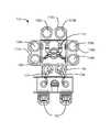
本発明の手法による処理チャンバ400の簡略化された概略図である図4を参照する。チャンバ400は、前述したすべての構成要素を含むことができ、チャンバの処理領域433に半導体基板455を収納するように構成することができる。基板455は、図示したように、ペデスタル465に位置づけすることができる。処理チャンバ400は、2つの遠隔プラズマシステム(RPS)401、402を含むことができる。第1のRPSユニット401は、チャンバ400の第1のアクセス405に流動的に結合させることができ、第1のアクセス405を介してチャンバ400の中へ第1の前駆体を送るように構成することができる。第2のRPSユニット402は、チャンバ400の第2のアクセス410に流動的に結合させることができ、第2のアクセス410を介してチャンバ400の中へ第2の前駆体を送るように構成することができる。第1のプラズマユニット401及び第2のプラズマユニット402は、同じ又は異なるプラズマシステムであってよい。例えば、片方又は両方のシステムが、RFプラズマシステム、CCPプラズマチャンバ、ICPプラズマチャンバ、トロイダルプラズマシステムを含む磁気生成プラズマシステム、マイクロ波プラズマシステム等、又はプラズマを形成することができる、又はそうでない場合にシステムにおいて分子を励起させる、及び/又は解離させることができる種類のその他任意のシステムであってよい。システムは、第1の前駆体及び第2の前駆体がチャンバ400の処理領域433に送られるまで、第1の前駆体及び第2の前駆体を互いに流動的に分離された状態に維持するように構成することができる。第1のアクセス405は、処理チャンバ400の最上部の近く、又はチャンバの最上部に位置づけすることができ、第2のアクセス410は、チャンバ400の側面部の一つの近く、又はそれに沿って位置づけすることができる。 Reference is made to FIG. 4, which is a simplified schematic diagram of a
チャンバ400はさらに、チャンバ内部にガス分配アセンブリ425を含むことができる。前述したデュアルチャネルシャワーヘッドの態様と類似していて良いガス分配アセンブリ425は、チャンバ400内部の処理領域433の最上部、又は処理領域433の上に位置づけすることができる。ガス分配アセンブリ425は、第1の前駆体及び第2の前駆体の両方を、チャンバ400の処理領域433の中へ送るように構成することができる。図4の例示のシステムはデュアルチャネルシャワーヘッドを含むが、当然ながら、処理領域433へ到達する前に第1及び第2の前駆体を流動的に分離された状態に維持する代替の分配アセンブリを用いることができる。例えば、穴あきプレートと、プレートの下の管を用いることができるが、効率が落ちる、又は記載されたデュアルチャネルシャワーヘッドのような処理の均一性が得られないその他の構成で作動させることができる。 The
ガス分配アセンブリ425は、前述したように、上方プレート420と下方プレート423を含むことができる。プレートを互いに結合させて、プレート間の容積427を画定することができる。上方プレートと下方プレートを通る第1の流体チャネル440と、下方プレート423を通る第2の流体チャネル445を提供するように、プレートを結合させることができる。形成されたチャネルを、下方プレート423を介して容積427から流動的にアクセスできるように構成することができ、第1の流体チャネル440を、複数のプレートと、第2の流体チャネル445との間の容積427から流動的に分離させることができる。容積427は、前述したチャネル322等のガス分配アセンブリ425の側面を介して流動的にアクセス可能である。ガス分配アセンブリのこの部分を、RPSユニット402がそれを介して第2の前駆体を送ることができるチャンバの第2のアクセス410に流動的に結合させることができる。 The
チャンバは、第1の前駆体を、チャンバの第1のアクセス405を介して、第1のRPSユニット401からチャンバの処理領域433へ送るように構成することができる。第1の前駆体を次に、ガス分配アセンブリ425の第1の流体チャネル440を介して送ることができる。チャンバはさらに、チャンバ400の第2のアクセス410を介して、第2のRPS402からチャンバの中へ第2の前駆体を供給するように構成することができる。第2の前駆体は、アクセス410を介して、ガス分配アセンブリ425の中へ流すことができる。第2の前駆体は、ガス分配アセンブリを介して、上方プレートと下方プレートとの間に画定された容積427の中へ流した後に、ガス分布アセンブリ425の下方プレート423の第2の流体チャネル445を介して処理領域433の中へ流すことができる。上方プレート420と下方プレート423の結合と構成から、アセンブリを、第2の前駆体のアセンブリ425の上方プレート420を通る流れを防止するように構成することができる。これは、前述したアセンブリの開孔が直線に並んでいるためでありうる。 The chamber may be configured to send a first precursor from the
RPSユニット401、402のプラズマキャビティと、チャンバのアクセス405、410につながるすべての機械的結合は、RPSユニット401、402を通って流れるように選択された第1の前駆体と第2の前駆体に基づく物質でできていてよい。例えば、特定のエッチング工程において、フッ素含有前駆体(例:NF3)を、例えばRPSユニット401等の第1のRPSユニット及び第2のRPSユニットのいずれかを介して流すことができる。RPSユニット401でプラズマが形成されると、分子はラジカルイオンに解離しうる。RPSユニット401が変質していないアルミニウムでできている場合、フッ素ラジカルはキャビティの壁と反応し、フッ化アルミニウム等の副産物を形成しうる。したがって、RPSユニット401を、例えば酸化アルミニウム、窒化アルミニウムであってよい第1の物質、又は第1の前駆体が相互作用を起こさない別の物質で形成することができる。RPSユニット401の物質は、第1の前駆体の組成に基づいて選択することができ、特に前駆体がチャンバの構成要素と相互作用しないように選択することができる。All mechanical couplings leading to the plasma cavities of the
同様に、第2のRPSユニット402は、第2の前駆体に基づいて選択された第2の物質でできていてよい。本発明の実施形態では、第1の物質及び第2の物質は異なる物質であってよい。例えば、水素含有前駆体を第2のRPS402を介して流した場合、プラズマが形成され、解離した水素ラジカルがRPS402のプラズマキャビティと相互作用を起こす場合がある。チャンバが同様に例えば酸化アルミニウムでできている場合、水素ラジカルが酸化物と相互作用を起こし、保護コーティングが剥離する場合がある。したがって、RPSユニット402は、第2の前駆体が相互作用を起こさないアルミニウム、又は別の物質等の第1の物質とは異なる第2の物質でできていてよい。これもガス分配アセンブリまで延在していてよく、上方プレート420の上面は第1のRPSで使用されるのと同じ物質でできている、又はそれでコーティングされており、上方プレート420の下面と、下方プレート423の上面は第2のRPSで使用される同じ物質でできている、又はそれでコーティングされている。上記コーティング又は物質の選択により、経時的な機器の劣化を改善することができる。したがって、ガス分配アセンブリのプレートはそれぞれ、一又は複数の物質でできた複数のプレートを含むことができる。 Similarly, the
作動中に、RPSユニット401、402のいずれか、あるいは両方を使用してユニット内部にプラズマを生じさせて、第1の前駆体及び/又は第2の前駆体を少なくとも部分的にイオン化することができる。フッ素含有前駆体と、水素含有前駆体を用いた一例では、水素含有前駆体を第1のRPSユニット401を介して流すことができ、フッ素含有ラジカルを第2のRPSユニット402を介して流すことができる。上記構成は、ラジカル種の移動距離に基づくものであってよい。例えば、処理領域433への経路は、第1のRPSユニット401よりも短い場合がある。水素ラジカルは半減期が短いために、フッ素ラジカルよりも速く再結合しうるため、水素含有ラジカルを短い経路を介して流すことができる。加えて、前述したように、ラジカル種を長持ちさせる、継続させる、又は強化するために、チャンバ400の領域のガス分配アセンブリ425の上でプラズマを形成することができる。しかしながら、本発明のその他の構成では、水素含有前駆体を第2のRPSユニット402を介して流すことができる。 During operation, either or both of the
RPSユニット401、402は、様々な実施形態において、約10W以下〜約10又は15kW以上の電力レベルで作動することができる。発明者は、各RPSユニットの電力及びプラズマプロファイルを、使用する特定の前駆体に対して調整できる本発明の手法のさらなる利点を有利に確定している。例えば、続けてフッ素含有前駆体、及び水素含有前駆体の例において、ある従来のシステムでは、解離が必要な前駆体が両方、同じRPSユニットを通って流れる必要がある。上述したプラズマキャビティとRPSユニットの潜在的な劣化に加え、前駆体の両方にとって有益なプラズマプロファイルは利用可能ではない場合がある。続けてこの例においては、NF3を含むフッ素含有前駆体を、RPSユニットの比較的低い電力レベルで処理することができる。100W、200W、400W未満〜1000W以上の電力レベルでRPSを作動させることによって、前駆体は粒子を完全にイオン化せず、NF及びNF2種も含む個々のラジカルを含む低い度合いまで解離することが可能である。さらに、水素含有前駆体を処理するRPSユニットは、完全な解離が所望されうる場合、はるかに高い電力レベルで作動させることができる。したがって、RPSユニットを最大約1000W以上で、また最大約10kW以上で作動させることができる。例示の処理システムで適用されるRF周波数は、異なる実施形態において、約500kHz未満の低いRF周波数、約10MHz〜15MHzの高いRF周波数、又は約1GHz以上のマイクロ波周波数であってよい。このように、第1のRPSユニット401は、第1の前駆体の組成に基づいて選択された第1の電力レベルで作動するように構成することができ、第2のRPSは、第2の前駆体の組成に基づいて選択された第2の電力レベルで作動するように構成することができる。2つのRPSユニット401、402を、互いに異なる電力レベルで作動するように構成することができる。上記の構成は、その他の変更の中でもとりわけ別々の電源、又は分離した電源を必要としうる。
RPSユニットのうちの一方を作動させ、他方を作動させないことによって、さらなる柔軟性を得ることができる。例えば、フッ素含有前駆体を、前駆体に基づいて低いレベルであってよい電力レベルで作動するように構成された第1のRPSユニット401を介して流すことができる。水素含有前駆体を、分子前駆体が処理領域433へ流れるようにプラズマが形成されない第2のRPSユニット402を介して流すことができる。第1の前駆体と、第2の前駆体がガス分配アセンブリ425を別々に出た時に第1の前駆体と第2の前駆体の相互作用が起こる可能性があり、RPSユニット401で少なくとも部分的にラジカル化されている第1の前駆体が第2の前駆体の一部をイオン化する可能性があり、この場合、システムの電力効率が改善されうる。当然ながら、これらの実施例に基づき、多数の態様を、様々な作動特性に基づく本発明の手法の実施形態において反転させる、又は変更することができる。 More flexibility can be gained by operating one of the RPS units and not operating the other. For example, the fluorine-containing precursor can be flowed through a
本発明をより理解し認識するために、本発明の実施形態による、特にシリコン選択エッチングであるエッチングプロセスのフロー図である図5を参照する。当然ながら、この手法を同様に堆積プロセスに用いることができる。シリコンは非結晶質、結晶質、又は多結晶(この場合は普通ポリシリコンと呼ばれる)であってよい。第1の工程の前に、構造をパターン付基板に形成することができる。この構造は、シリコン、及び酸化シリコンの別々の露出領域を有することができる。前の堆積及び形成プロセスは、同じチャンバで行われていても、行われていなくてもよい。異なるチャンバで行われた場合、基板は上述したようにシステムへ転送することができる。 To better understand and appreciate the present invention, reference is made to FIG. 5, which is a flow diagram of an etching process, particularly silicon selective etching, according to an embodiment of the present invention. Of course, this approach can be used in the deposition process as well. Silicon may be amorphous, crystalline, or polycrystalline (in this case commonly referred to as polysilicon). Prior to the first step, the structure can be formed on the patterned substrate. This structure can have separate exposed regions of silicon and silicon oxide. The previous deposition and formation process may or may not be performed in the same chamber. If done in a different chamber, the substrate can be transferred to the system as described above.
第1の前駆体、例えば水素含有前駆体を、工程510において基板の処理領域とは別に、第1のプラズマ領域の中へ流すことができる。別々のプラズマ領域を本明細書では遠隔プラズマ領域と呼ばれる場合があり、処理チャンバとは違うモジュール、又は処理チャンバ内部の区画部分の中にあってよい。一般的に言えば、水素含有前駆体を第1のプラズマ領域の中へ流してプラズマ内で励起させることができ、水素含有前駆体は、H2、NH3、炭化水素等から選択された少なくとも一つの前駆体を含むことができる。第2の前駆体、例えば三フッ化窒素、又は別のフッ素含有前駆体の流れを、工程520において第2の遠隔プラズマシステムの中へ導入して、プラズマ内で励起させることができる。第1のプラズマシステム、及び第2のプラズマシステムを前述したように任意のやり方で作動させることができ、本発明の実施形態では、水素含有前駆体とフッ素含有前駆体を代替のRPSユニットを介して流すことができる。加えて、遠隔プラズマシステムのうちの一方のみを本発明の実施形態において作動させることができる。三フッ化窒素の流動率を水素の流動率に対して遅くして、簡単に定量化される高い原子流動率H:Fを実現することができる。その他のフッ素供給源を使用して、三フッ化窒素を補強する、又は置換することができる。一般に、フッ素含有前駆体を第2の遠隔プラズマ領域に流すことができ、フッ素含有前駆体は、原子フッ素、二原子フッ素、三フッ化臭素、三フッ化塩素、三フッ化窒素、フッ化水素、フッ素化炭化水素、六フッ化硫黄、二フッ化キセノンからなる群から選択される少なくとも一つの前駆体を含む。A first precursor, such as a hydrogen-containing precursor, can be flowed into the first plasma region in
第1の前駆体及び第2の前駆体の遠隔プラズマ領域に形成されたプラズマ廃液を次に、工程530において基板処理領域の中へ別々に流し、基板処理領域へ組み込むことができる。パターン化基板を選択的にエッチングすることにより、露出した酸化シリコンの少なくとも、又は約70倍の比率で露出したシリコンを除去することができる。この手法には、シリコンのエッチング選択性を高めるために、フッ素(F)に対する水素(H)の高い原子流量比の維持が含まれうる。幾つかの前駆体はフッ素と水素を両方含むことができ、この場合、本明細書に記載される原子流量比を計算する時に、すべての構成物の原子流動率が含まれる。水素の量の優位性により、パターン化基板上の露出面を水素終端しやすくなりうる。本明細書に記載された条件下で、水素終端は、シリコン表面でのみ準安定原子でありうる。三フッ化窒素又はその他のフッ素含有前駆体のフッ素によりシリコン表面の水素が置換され、表面から剥離してシリコンを取り除く揮発性残留物ができる。他の露出した物質に存在する結合エネルギーが強いために、フッ素は他の水素終端面の水素を置換することができない場合がある(及び/又は他の露出した物質を除去する揮発性残留物ができない可能性がある)。 The plasma effluent formed in the remote plasma region of the first precursor and the second precursor can then be separately flowed into the substrate processing region at
一例では、約15:1以上のガス流量比(H2:NF3)、又は一般論として、約10:1以上の原子流量比により、約70:1以上のエッチング選択性(シリコン:酸化シリコン、又はシリコン:窒化シリコン)が得られることがわかっている。エッチング選択性(シリコン:酸化シリコン、又はシリコン:窒化シリコン)は、本発明の実施形態において、約100:1以上、約150:1以上、約200:1以上、約250:1以上、又は約300:1以上であってもよい、又はこれらの範囲のうちの任意の範囲の間、又はこれらの範囲のうちの任意の範囲内であってもよい。パターン化基板には、タングステン、窒化チタン、又はその他の金属が露出した領域も存在する場合があり、露出した金属領域と呼ぶことができる。エッチング選択性(シリコン:露出した金属領域)は、本発明の実施形態では、約100:1以上、約150:1以上、約200:1以上、約250:1以上、約500:1以上、約1000:1以上、約2000:1以上、又は約3000:1以上であってよい。反応性化学種が基板処理領域から取り除かれ、次に基板が処理領域から取り除かれる。In one example, a gas flow ratio (H2 : NF3 ) of about 15: 1 or greater, or, generally, an atomic flow ratio of about 10: 1 or greater provides an etch selectivity of about 70: 1 (silicon: silicon oxide). Or silicon: silicon nitride). Etch selectivity (silicon: silicon oxide, or silicon: silicon nitride) is about 100: 1 or higher, about 150: 1 or higher, about 200: 1 or higher, about 250: 1 or higher, or about 250: 1 or higher in embodiments of the present invention. It may be 300: 1 or more, or between any of these ranges, or within any of these ranges. The patterned substrate may also have exposed regions of tungsten, titanium nitride, or other metals, which can be referred to as exposed metal regions. Etch selectivity (silicon: exposed metal region) is about 100: 1 or more, about 150: 1 or more, about 200: 1 or more, about 250: 1 or more, about 500: 1 or more in an embodiment of the present invention, It may be about 1000: 1 or more, about 2000: 1 or more, or about 3000: 1 or more. The reactive species are removed from the substrate processing area, and then the substrate is removed from the processing area.
本明細書に記載されるように、大流量の水素含有前駆体が存在することにより、シリコン、酸化シリコン及び窒化シリコンが処理のほとんどの過程において水素終端面が確実に維持される。フッ素含有前駆体及び/又は水素含有前駆体はさらに、He、N2、Ar等の一又は複数の比較的不活性なガスを含むことができる。不活性ガスを使用して、プラズマの安定性を改善する、及び/又は液状の前駆体を遠隔プラズマ領域まで送ることができる。異なるガスの流動率及び流量比を使用して、エッチング速度及びエッチング選択性を制御することができる。一実施形態では、フッ素含有ガスは、流動率が約1〜30sccm(立方センチメートル/分)のNF3と、流動率が約500〜5000sccmのH2と、流動率が約0〜3000sccmのHeと、流動率が約0〜3000sccmのArを含む。本発明の実施形態では、原子流量比H:Fを高く維持して、酸化シリコン上への固体残留物の形成を減らす、又はなくすことができる。固体残留物の形成により、酸化シリコンの一部が消費されるため、エッチングプロセスのシリコン選択性が低下しうる。原子流量比H:Fは、この手法の実施形態では、約25(すなわち25:1)以上、約30:1以上、又は約40:1以上であってよい。As described herein, the presence of a high flow rate of hydrogen-containing precursor ensures that the hydrogen termination surface is maintained during most of the processing of silicon, silicon oxide and silicon nitride. The fluorine-containing precursor and / or the hydrogen-containing precursor can further include one or more relatively inert gases such as He, N2 , Ar. An inert gas can be used to improve plasma stability and / or to deliver a liquid precursor to the remote plasma region. Different gas flow rates and flow ratios can be used to control etch rate and etch selectivity. In one embodiment, the fluorine-containing gas includes NF3 with a flow rate of about 1-30 sccm (cubic centimeters / minute), H2 with a flow rate of about 500-5000 sccm, He with a flow rate of about 0-3000 sccm, It contains Ar with a flow rate of about 0 to 3000 sccm. In embodiments of the present invention, the atomic flow ratio H: F can be kept high to reduce or eliminate the formation of solid residues on the silicon oxide. The formation of the solid residue consumes a portion of the silicon oxide, which can reduce the silicon selectivity of the etching process. The atomic flow ratio H: F may be about 25 (ie 25: 1) or more, about 30: 1 or more, or about 40: 1 or more in embodiments of this approach.
前駆体を流動的に分離した状態に維持することで、腐食、またRPSシステムとのその他の相互作用を減らす、又はなくすことができる。上述したように、ガス分配アセンブリを含むRPSユニット及び分配構成要素は、送られる前駆体に基づいて選択され、したがってイオン化前駆体と機器との間の反応を防止するように選択された物質でできていてよい。 By keeping the precursor fluidly separated, corrosion and other interactions with the RPS system can be reduced or eliminated. As mentioned above, the RPS unit and distribution components including the gas distribution assembly are selected based on the precursor being delivered and thus can be made of materials selected to prevent reaction between the ionization precursor and the instrument. It may be.
本発明の実施形態では、遠隔プラズマ領域から基板処理領域まで通過する間に、イオンサプレッサーを使用して、プラズマ廃液からのイオンをフィルタリングすることができる。イオンサプレッサーは、プラズマ生成領域から基板まで移動しているイオン的に帯電した種を減らす又はなくすように機能する。荷電されていない中性種及びラジカル種は、イオンサプレッサーの開口部を通過して基板において反応しうる。基板周囲の反応領域からイオン的に荷電した種を完全に除去することが必ずしも望ましい目的でないことに留意されたい。多くの場合、エッチング及び/又は堆積プロセスを行うためには、基板に到達するのにイオン種が必要である。これらの場合、イオンサプレッサーにより、プロセスを支援するレベルで、反応領域のイオン種の濃度を制御しやすくなる。本発明の実施形態では、ガス分配アセンブリの上方プレートはイオンサプレッサーを含むことができる。 In embodiments of the present invention, an ion suppressor can be used to filter ions from the plasma effluent while passing from the remote plasma region to the substrate processing region. The ion suppressor functions to reduce or eliminate ionically charged species moving from the plasma generation region to the substrate. Uncharged neutral and radical species can react at the substrate through the opening of the ion suppressor. Note that it is not always desirable to completely remove ionically charged species from the reaction region around the substrate. In many cases, an ionic species is required to reach the substrate in order to perform an etching and / or deposition process. In these cases, the ion suppressor makes it easier to control the concentration of ion species in the reaction region at a level that supports the process. In an embodiment of the invention, the upper plate of the gas distribution assembly can include an ion suppressor.
エッチングプロセスの間の基板の温度は、0℃超であってよい。基板の温度はあるいは、約20℃以上、及び約300℃以下であってよい。この基板の温度範囲の上限値において、シリコンのエッチング速度は低下しうる。この基板の温度範囲の下限値において、酸化シリコンと窒化シリコンのエッチングが始まりうるため、選択性が低下しうる。本発明の実施形態では、本明細書に記載されたエッチングの間の基板の温度は、約30℃以上、及び約200℃以下、又は約40℃以上、及び約150℃以下であってよい。基板の温度は、本発明の実施形態において、100℃未満、約80℃以下、約65℃以下、又は約50℃以下であってよい。 The temperature of the substrate during the etching process may be greater than 0 ° C. The substrate temperature may alternatively be about 20 ° C. or higher and about 300 ° C. or lower. At the upper limit of the temperature range of the substrate, the silicon etching rate can be reduced. Since the etching of silicon oxide and silicon nitride can start at the lower limit of the temperature range of the substrate, the selectivity can be lowered. In embodiments of the invention, the temperature of the substrate during the etching described herein may be about 30 ° C. or higher and about 200 ° C. or lower, or about 40 ° C. or higher and about 150 ° C. or lower. The temperature of the substrate may be less than 100 ° C., about 80 ° C. or less, about 65 ° C. or less, or about 50 ° C. or less in embodiments of the present invention.
データはさらに、(所定の水素:フッ素原子比に対して)シリコンのエッチング速度の上昇をプロセス圧の関数として示す。しかしながら、約50:1のH:Fの原子流動率に対し、1Torrを超える圧力の上昇により、選択性が低下し始めうる。これは、2以上のフッ素含有廃液の混合の確率が高いことが原因と考えられる。エッチングプロセスでは次に、酸化シリコン、窒化シリコン、及び他の物質の除去が開始される。基板処理領域内の圧力は、本発明の実施形態において、約10Torr以下、約5Torr以下、約3Torr以下、約2Torr以下、約1Torr以下、又は約750mTorr以下であってよい。本発明の実施形態において、十分なエッチング速度を確保するためには、圧力は約0.05Torr以上、約0.1Torr以上、約0.2Torr以上、又は約0.4Torr以上であってよい。さらなる実施例、プロセスパラメータ、及び作動ステップは、本明細書に記載された供給機構と反しない範囲で、前に組み込まれた特許出願第13/439079号明細書に含まれている。 The data further shows the increase in silicon etch rate (for a given hydrogen: fluorine atomic ratio) as a function of process pressure. However, for an atomic flow rate of about 50: 1 H: F, the selectivity may begin to decrease with a pressure increase of over 1 Torr. This is considered due to the high probability of mixing two or more fluorine-containing waste liquids. The etching process then begins to remove silicon oxide, silicon nitride, and other materials. The pressure in the substrate processing region may be about 10 Torr or less, about 5 Torr or less, about 3 Torr or less, about 2 Torr or less, about 1 Torr or less, or about 750 mTorr or less in embodiments of the present invention. In embodiments of the present invention, the pressure may be about 0.05 Torr or more, about 0.1 Torr or more, about 0.2 Torr or more, or about 0.4 Torr or more to ensure a sufficient etch rate. Further examples, process parameters, and operating steps are included in previously incorporated patent application 13/439079, to the extent that they do not conflict with the feed mechanism described herein.
上述の説明では、説明の目的のために、本発明の様々な実施形態の理解を促すために、多数の詳細が記載されてきた。しかしながら、特定の実施形態をこれらの詳細の幾つかの詳細なしで、又は更なる詳細と共に実行することができることが当業者には明らかとなるであろう。 In the above description, for purposes of explanation, numerous details have been set forth in order to facilitate understanding of various embodiments of the present invention. However, it will be apparent to one skilled in the art that certain embodiments may be practiced without some of these details or with further details.
幾つかの実施形態を開示したが、当然ながら当業者には、本発明の実施形態の主旨から逸脱することなく、様々な変更例、代替構造物、及び同等物を使用することができることが理解されるだろう。加えて、任意の数の周知のプロセス、及び要素は、本発明が不必要に曖昧にならないように記載していない。したがって上記の記載により、本発明の範囲を限定するものと解釈すべきでない。 While several embodiments have been disclosed, it will be appreciated by those skilled in the art that various modifications, alternative constructions, and equivalents may be used without departing from the spirit of the embodiments of the present invention. Will be done. In addition, any number of well-known processes and elements have not been described so as not to unnecessarily obscure the present invention. Therefore, the above description should not be taken as limiting the scope of the invention.
値の範囲が付与されているところでは、文脈上そうでないと明示されていない限り、当然ながら、その範囲の上限値と下限値との間の各介在値は、下限値の最も小さい単位まで具体的に開示されている。記載された範囲の任意の記載値又は記載されていない介在値の間の任意の小さい範囲、そしてその記載範囲のその他任意の記載された又は介在する値も含まれる。これら小さい範囲の上限値及び下限値は、その範囲に個々に含まれ、又はその範囲から除外される場合があり、小さい範囲に限界値のいずれかが含まれる、どちらも含まれない、又は両方が含まれる各範囲もこの手法に含まれ、記載された範囲において任意に具体的に除外された限界値に依存する。記載された範囲に一又は複数の限界値が含まれるところでは、これらの含有限界値のいずれか、又は両方を除外する範囲も含まれる。 Where a range of values is given, each intervening value between the upper and lower limits of the range is, of course, specified to the smallest unit of the lower limit unless explicitly stated otherwise in the context. Have been disclosed. Also included are any stated values in the stated range or any small range between undescribed intervening values, and any other stated or intervening values in that stated range. The upper and lower limits of these small ranges may be individually included or excluded from the range, and any of the limit values may be included in the small range, neither, or both Each range that includes is also included in this approach and depends on the limit values that are arbitrarily specifically excluded in the stated range. Where one or more limit values are included in the stated range, ranges that exclude either or both of these limit values are also included.
本明細書及び添付の特許請求の範囲で使用される単数形「1つの(a)」、「1つの(an)」、及び「その(the)」は、文脈上別途明示しない限り複数の指示物を含む。したがって、例えば、「開孔」を参照した時は複数の上記開孔を含み、「プレート」を参照した時は、一又は複数のプレート及び当業者に周知のそれらの同等物他への参照を含む。 As used in this specification and the appended claims, the singular forms “a”, “an”, and “the” include plural referents unless the context clearly dictates otherwise. Including things. Thus, for example, reference to “aperture” includes a plurality of such apertures, and reference to “plate” refers to a reference to one or more plates and their equivalents known to those skilled in the art. Including.
また、「備える(comprise(s))」、「備えている(comprising)」、「含有する(contain(s))」、「含有している(containing)」、「含む(include(s))」、及び「含んでいる(including)」という単語は、本明細書及び特許請求の範囲で使用された場合、記載された特徴、整数、構成要素、又はステップの存在を特定することを意図しているが、一又は複数のその他の特徴、整数、構成要素、ステップ、作動、又はグループの存在、又は追加を除外するものではない。 Also, “comprise (s)”, “comprising”, “contain (s)”, “containing”, “include (s)” And the word “including”, as used in the specification and claims, are intended to identify the presence of the described feature, integer, component, or step. This does not exclude the presence or addition of one or more other features, integers, components, steps, operations, or groups.
Claims (20)
Translated fromJapaneseチャンバの処理領域に半導体基板を収納するように構成された前記チャンバと、
前記チャンバの第1のアクセスに流動的に結合され、前記第1のアクセスを介して前記チャンバの中へ第1の前駆体を送るように構成された第1の遠隔プラズマシステムと、
前記チャンバの第2のアクセスに流動的に結合され、前記第2のアクセスを介して前記チャンバの中へ第2の前駆体を送るように構成された第2の遠隔プラズマシステムと、
前記第1の前駆体と前記第2の前駆体の両方を前記チャンバの前記処理領域の中へ送るように構成されたガス分配アセンブリであって、前記ガス分配アセンブリは、前記第1の前駆体と前記第2の前駆体が前記チャンバの前記処理領域へ送られるまで、前記第1の前駆体と前記第2の前駆体を互いに流動的に分離された状態に維持するように構成されており、前記ガス分配アセンブリのうちの前記第1の前駆体と接する第1の部分は、前記第1の前駆体と相互作用しない物質でできており、前記ガス分配アセンブリのうちの前記第2の前駆体と接する第2の部分は、前記第2の前駆体と相互作用しない物質でできている、ガス分配アセンブリと、を備えるシステム。A system for semiconductor processing,
The chamber configured to receive a semiconductor substrate in a processing region of the chamber;
A first remote plasma system fluidly coupled to a first access of the chamber and configured to deliver a first precursor into the chamber via the first access;
A second remote plasma system fluidly coupled to a second access of the chamber and configured to deliver a second precursor into the chamber via the second access;
A gas distribution assembly configured to deliver both the first precursor and the second precursor into the processing region of the chamber, the gas distribution assemblycomprising the first precursor And the second precursor is configured to be fluidly separated from each other until the second precursor is delivered to the processing region of the chamber. A first portion of the gas distribution assembly that contacts the first precursor is made of a material that does not interact with the first precursor, and the second precursor of the gas distribution assembly. A system comprising: a gas distribution assembly, wherein the second portion in contact with the body is made of a material that does not interact with the second precursor .
第1の前駆体を第1の遠隔プラズマシステムを介して半導体処理チャンバの中へ流すことと、
第2の前駆体を第2の遠隔プラズマシステムを介して半導体処理チャンバの中へ流すことと
を含み、前記第1の前駆体および前記第2の前駆体の両方は、ガス分配アセンブリにより前記処理チャンバの処理領域の中に送られ、前記第1の前駆体と、前記第2の前駆体は、前記処理領域において混合され、前記ガス分配アセンブリは、前記第1の前駆体と前記第2の前駆体が前記チャンバの前記処理領域へ送られるまで、前記第1の前駆体と前記第2の前駆体を互いに流動的に分離された状態に維持するように構成されており、前記ガス分配アセンブリのうちの前記第1の前駆体と接する第1の部分は、前記第1の前駆体と相互作用しない物質でできており、前記ガス分配アセンブリのうちの前記第2の前駆体と接する第2の部分は、前記第2の前駆体と相互作用しない物質でできている、方法。A method for operating a semiconductor processing chamber comprising:
Flowing a first precursor through a first remote plasma system into a semiconductor processing chamber;
Flowing a second precursor through a second remote plasma system into a semiconductor processing chamber, wherein both the first precursor and the second precursor are processed by the gas distribution assembly. And the first precursor and the second precursor are mixed in the processing region, andthe gas distribution assembly includes the first precursor and the second precursor. The gas distribution assembly is configured to maintain the first precursor and the second precursor fluidly separated from each other until the precursor is delivered to the processing region of the chamber. A first portion in contact with the first precursor is made of a material that does not interact with the first precursor, and a second portion in contact with the second precursor of the gas distribution assembly. Part of the second Made of not interact with the precursor material, method.
Applications Claiming Priority (5)
| Application Number | Priority Date | Filing Date | Title |
|---|---|---|---|
| US201261704241P | 2012-09-21 | 2012-09-21 | |
| US61/704,241 | 2012-09-21 | ||
| US13/799,490US20140099794A1 (en) | 2012-09-21 | 2013-03-13 | Radical chemistry modulation and control using multiple flow pathways |
| US13/799,490 | 2013-03-13 | ||
| PCT/US2013/057599WO2014046864A1 (en) | 2012-09-21 | 2013-08-30 | Radical chemistry modulation and control using multiple flow pathways |
Publications (2)
| Publication Number | Publication Date |
|---|---|
| JP2015532016A JP2015532016A (en) | 2015-11-05 |
| JP6392760B2true JP6392760B2 (en) | 2018-09-19 |
Family
ID=50341849
Family Applications (1)
| Application Number | Title | Priority Date | Filing Date |
|---|---|---|---|
| JP2015533084AExpired - Fee RelatedJP6392760B2 (en) | 2012-09-21 | 2013-08-30 | Regulation and control of radical chemistry using multiple flow paths |
Country Status (6)
| Country | Link |
|---|---|
| US (1) | US20140099794A1 (en) |
| JP (1) | JP6392760B2 (en) |
| KR (1) | KR102114002B1 (en) |
| CN (2) | CN104641456A (en) |
| TW (1) | TWI663646B (en) |
| WO (1) | WO2014046864A1 (en) |
Families Citing this family (460)
| Publication number | Priority date | Publication date | Assignee | Title |
|---|---|---|---|---|
| US9394608B2 (en) | 2009-04-06 | 2016-07-19 | Asm America, Inc. | Semiconductor processing reactor and components thereof |
| US8802201B2 (en) | 2009-08-14 | 2014-08-12 | Asm America, Inc. | Systems and methods for thin-film deposition of metal oxides using excited nitrogen-oxygen species |
| US9324576B2 (en) | 2010-05-27 | 2016-04-26 | Applied Materials, Inc. | Selective etch for silicon films |
| US10283321B2 (en) | 2011-01-18 | 2019-05-07 | Applied Materials, Inc. | Semiconductor processing system and methods using capacitively coupled plasma |
| US8999856B2 (en) | 2011-03-14 | 2015-04-07 | Applied Materials, Inc. | Methods for etch of sin films |
| US9064815B2 (en) | 2011-03-14 | 2015-06-23 | Applied Materials, Inc. | Methods for etch of metal and metal-oxide films |
| US20130023129A1 (en) | 2011-07-20 | 2013-01-24 | Asm America, Inc. | Pressure transmitter for a semiconductor processing environment |
| US8808563B2 (en) | 2011-10-07 | 2014-08-19 | Applied Materials, Inc. | Selective etch of silicon by way of metastable hydrogen termination |
| US9017481B1 (en) | 2011-10-28 | 2015-04-28 | Asm America, Inc. | Process feed management for semiconductor substrate processing |
| US9267739B2 (en) | 2012-07-18 | 2016-02-23 | Applied Materials, Inc. | Pedestal with multi-zone temperature control and multiple purge capabilities |
| US9373517B2 (en) | 2012-08-02 | 2016-06-21 | Applied Materials, Inc. | Semiconductor processing with DC assisted RF power for improved control |
| US9121097B2 (en)* | 2012-08-31 | 2015-09-01 | Novellus Systems, Inc. | Variable showerhead flow by varying internal baffle conductance |
| US9034770B2 (en) | 2012-09-17 | 2015-05-19 | Applied Materials, Inc. | Differential silicon oxide etch |
| US9023734B2 (en) | 2012-09-18 | 2015-05-05 | Applied Materials, Inc. | Radical-component oxide etch |
| US9390937B2 (en) | 2012-09-20 | 2016-07-12 | Applied Materials, Inc. | Silicon-carbon-nitride selective etch |
| US9132436B2 (en)* | 2012-09-21 | 2015-09-15 | Applied Materials, Inc. | Chemical control features in wafer process equipment |
| US10714315B2 (en) | 2012-10-12 | 2020-07-14 | Asm Ip Holdings B.V. | Semiconductor reaction chamber showerhead |
| US8969212B2 (en) | 2012-11-20 | 2015-03-03 | Applied Materials, Inc. | Dry-etch selectivity |
| US8980763B2 (en) | 2012-11-30 | 2015-03-17 | Applied Materials, Inc. | Dry-etch for selective tungsten removal |
| US9111877B2 (en) | 2012-12-18 | 2015-08-18 | Applied Materials, Inc. | Non-local plasma oxide etch |
| US8921234B2 (en) | 2012-12-21 | 2014-12-30 | Applied Materials, Inc. | Selective titanium nitride etching |
| US20160376700A1 (en) | 2013-02-01 | 2016-12-29 | Asm Ip Holding B.V. | System for treatment of deposition reactor |
| US10256079B2 (en) | 2013-02-08 | 2019-04-09 | Applied Materials, Inc. | Semiconductor processing systems having multiple plasma configurations |
| US9362130B2 (en) | 2013-03-01 | 2016-06-07 | Applied Materials, Inc. | Enhanced etching processes using remote plasma sources |
| US9040422B2 (en) | 2013-03-05 | 2015-05-26 | Applied Materials, Inc. | Selective titanium nitride removal |
| US20140271097A1 (en) | 2013-03-15 | 2014-09-18 | Applied Materials, Inc. | Processing systems and methods for halide scavenging |
| US9493879B2 (en) | 2013-07-12 | 2016-11-15 | Applied Materials, Inc. | Selective sputtering for pattern transfer |
| US9773648B2 (en) | 2013-08-30 | 2017-09-26 | Applied Materials, Inc. | Dual discharge modes operation for remote plasma |
| US9576809B2 (en) | 2013-11-04 | 2017-02-21 | Applied Materials, Inc. | Etch suppression with germanium |
| US9520303B2 (en) | 2013-11-12 | 2016-12-13 | Applied Materials, Inc. | Aluminum selective etch |
| US9245762B2 (en) | 2013-12-02 | 2016-01-26 | Applied Materials, Inc. | Procedure for etch rate consistency |
| US9287095B2 (en) | 2013-12-17 | 2016-03-15 | Applied Materials, Inc. | Semiconductor system assemblies and methods of operation |
| US9287134B2 (en) | 2014-01-17 | 2016-03-15 | Applied Materials, Inc. | Titanium oxide etch |
| US9293568B2 (en) | 2014-01-27 | 2016-03-22 | Applied Materials, Inc. | Method of fin patterning |
| US9396989B2 (en) | 2014-01-27 | 2016-07-19 | Applied Materials, Inc. | Air gaps between copper lines |
| US9385028B2 (en) | 2014-02-03 | 2016-07-05 | Applied Materials, Inc. | Air gap process |
| US9499898B2 (en) | 2014-03-03 | 2016-11-22 | Applied Materials, Inc. | Layered thin film heater and method of fabrication |
| US9299575B2 (en) | 2014-03-17 | 2016-03-29 | Applied Materials, Inc. | Gas-phase tungsten etch |
| US11015245B2 (en) | 2014-03-19 | 2021-05-25 | Asm Ip Holding B.V. | Gas-phase reactor and system having exhaust plenum and components thereof |
| US9299538B2 (en) | 2014-03-20 | 2016-03-29 | Applied Materials, Inc. | Radial waveguide systems and methods for post-match control of microwaves |
| US9299537B2 (en) | 2014-03-20 | 2016-03-29 | Applied Materials, Inc. | Radial waveguide systems and methods for post-match control of microwaves |
| US9903020B2 (en) | 2014-03-31 | 2018-02-27 | Applied Materials, Inc. | Generation of compact alumina passivation layers on aluminum plasma equipment components |
| US9269590B2 (en) | 2014-04-07 | 2016-02-23 | Applied Materials, Inc. | Spacer formation |
| US9309598B2 (en) | 2014-05-28 | 2016-04-12 | Applied Materials, Inc. | Oxide and metal removal |
| US20150348755A1 (en)* | 2014-05-29 | 2015-12-03 | Charm Engineering Co., Ltd. | Gas distribution apparatus and substrate processing apparatus including same |
| US20150361582A1 (en)* | 2014-06-17 | 2015-12-17 | Veeco Instruments, Inc. | Gas Flow Flange For A Rotating Disk Reactor For Chemical Vapor Deposition |
| US9378969B2 (en) | 2014-06-19 | 2016-06-28 | Applied Materials, Inc. | Low temperature gas-phase carbon removal |
| US9406523B2 (en) | 2014-06-19 | 2016-08-02 | Applied Materials, Inc. | Highly selective doped oxide removal method |
| US9840777B2 (en)* | 2014-06-27 | 2017-12-12 | Applied Materials, Inc. | Apparatus for radical-based deposition of dielectric films |
| KR102247560B1 (en)* | 2014-07-14 | 2021-05-03 | 삼성전자 주식회사 | Plasma generating method in RPS(Remote Plasma Source) and method for fabricating semiconductor device comprising the same plasma generating method |
| US9425058B2 (en) | 2014-07-24 | 2016-08-23 | Applied Materials, Inc. | Simplified litho-etch-litho-etch process |
| US10858737B2 (en) | 2014-07-28 | 2020-12-08 | Asm Ip Holding B.V. | Showerhead assembly and components thereof |
| US20160032451A1 (en)* | 2014-07-29 | 2016-02-04 | Applied Materials, Inc. | Remote plasma clean source feed between backing plate and diffuser |
| US9378978B2 (en) | 2014-07-31 | 2016-06-28 | Applied Materials, Inc. | Integrated oxide recess and floating gate fin trimming |
| US9496167B2 (en) | 2014-07-31 | 2016-11-15 | Applied Materials, Inc. | Integrated bit-line airgap formation and gate stack post clean |
| US9659753B2 (en) | 2014-08-07 | 2017-05-23 | Applied Materials, Inc. | Grooved insulator to reduce leakage current |
| US9553102B2 (en) | 2014-08-19 | 2017-01-24 | Applied Materials, Inc. | Tungsten separation |
| US9890456B2 (en) | 2014-08-21 | 2018-02-13 | Asm Ip Holding B.V. | Method and system for in situ formation of gas-phase compounds |
| US9355856B2 (en) | 2014-09-12 | 2016-05-31 | Applied Materials, Inc. | V trench dry etch |
| JP6544902B2 (en)* | 2014-09-18 | 2019-07-17 | 東京エレクトロン株式会社 | Plasma processing system |
| US9368364B2 (en) | 2014-09-24 | 2016-06-14 | Applied Materials, Inc. | Silicon etch process with tunable selectivity to SiO2 and other materials |
| US9355862B2 (en) | 2014-09-24 | 2016-05-31 | Applied Materials, Inc. | Fluorine-based hardmask removal |
| US9613822B2 (en) | 2014-09-25 | 2017-04-04 | Applied Materials, Inc. | Oxide etch selectivity enhancement |
| US10941490B2 (en) | 2014-10-07 | 2021-03-09 | Asm Ip Holding B.V. | Multiple temperature range susceptor, assembly, reactor and system including the susceptor, and methods of using the same |
| US9355922B2 (en)* | 2014-10-14 | 2016-05-31 | Applied Materials, Inc. | Systems and methods for internal surface conditioning in plasma processing equipment |
| US9966240B2 (en) | 2014-10-14 | 2018-05-08 | Applied Materials, Inc. | Systems and methods for internal surface conditioning assessment in plasma processing equipment |
| US11637002B2 (en) | 2014-11-26 | 2023-04-25 | Applied Materials, Inc. | Methods and systems to enhance process uniformity |
| US9299583B1 (en) | 2014-12-05 | 2016-03-29 | Applied Materials, Inc. | Aluminum oxide selective etch |
| US10573496B2 (en) | 2014-12-09 | 2020-02-25 | Applied Materials, Inc. | Direct outlet toroidal plasma source |
| US10224210B2 (en) | 2014-12-09 | 2019-03-05 | Applied Materials, Inc. | Plasma processing system with direct outlet toroidal plasma source |
| US9502258B2 (en) | 2014-12-23 | 2016-11-22 | Applied Materials, Inc. | Anisotropic gap etch |
| US9343272B1 (en) | 2015-01-08 | 2016-05-17 | Applied Materials, Inc. | Self-aligned process |
| US11257693B2 (en) | 2015-01-09 | 2022-02-22 | Applied Materials, Inc. | Methods and systems to improve pedestal temperature control |
| US9373522B1 (en) | 2015-01-22 | 2016-06-21 | Applied Mateials, Inc. | Titanium nitride removal |
| US9449846B2 (en) | 2015-01-28 | 2016-09-20 | Applied Materials, Inc. | Vertical gate separation |
| US9728437B2 (en) | 2015-02-03 | 2017-08-08 | Applied Materials, Inc. | High temperature chuck for plasma processing systems |
| US20160225652A1 (en) | 2015-02-03 | 2016-08-04 | Applied Materials, Inc. | Low temperature chuck for plasma processing systems |
| US9881805B2 (en) | 2015-03-02 | 2018-01-30 | Applied Materials, Inc. | Silicon selective removal |
| US10276355B2 (en) | 2015-03-12 | 2019-04-30 | Asm Ip Holding B.V. | Multi-zone reactor, system including the reactor, and method of using the same |
| US12281385B2 (en)* | 2015-06-15 | 2025-04-22 | Taiwan Semiconductor Manufacturing Co., Ltd. | Gas dispenser and deposition apparatus using the same |
| US10458018B2 (en) | 2015-06-26 | 2019-10-29 | Asm Ip Holding B.V. | Structures including metal carbide material, devices including the structures, and methods of forming same |
| US9741593B2 (en) | 2015-08-06 | 2017-08-22 | Applied Materials, Inc. | Thermal management systems and methods for wafer processing systems |
| US9691645B2 (en) | 2015-08-06 | 2017-06-27 | Applied Materials, Inc. | Bolted wafer chuck thermal management systems and methods for wafer processing systems |
| US9349605B1 (en) | 2015-08-07 | 2016-05-24 | Applied Materials, Inc. | Oxide etch selectivity systems and methods |
| US10504700B2 (en) | 2015-08-27 | 2019-12-10 | Applied Materials, Inc. | Plasma etching systems and methods with secondary plasma injection |
| US10211308B2 (en) | 2015-10-21 | 2019-02-19 | Asm Ip Holding B.V. | NbMC layers |
| US11139308B2 (en) | 2015-12-29 | 2021-10-05 | Asm Ip Holding B.V. | Atomic layer deposition of III-V compounds to form V-NAND devices |
| US10529554B2 (en) | 2016-02-19 | 2020-01-07 | Asm Ip Holding B.V. | Method for forming silicon nitride film selectively on sidewalls or flat surfaces of trenches |
| US10343920B2 (en) | 2016-03-18 | 2019-07-09 | Asm Ip Holding B.V. | Aligned carbon nanotubes |
| US10190213B2 (en) | 2016-04-21 | 2019-01-29 | Asm Ip Holding B.V. | Deposition of metal borides |
| US10865475B2 (en) | 2016-04-21 | 2020-12-15 | Asm Ip Holding B.V. | Deposition of metal borides and silicides |
| US11066747B2 (en)* | 2016-04-25 | 2021-07-20 | Applied Materials, Inc. | Chemical delivery chamber for self-assembled monolayer processes |
| US10367080B2 (en) | 2016-05-02 | 2019-07-30 | Asm Ip Holding B.V. | Method of forming a germanium oxynitride film |
| US10504754B2 (en) | 2016-05-19 | 2019-12-10 | Applied Materials, Inc. | Systems and methods for improved semiconductor etching and component protection |
| US10522371B2 (en) | 2016-05-19 | 2019-12-31 | Applied Materials, Inc. | Systems and methods for improved semiconductor etching and component protection |
| US11453943B2 (en) | 2016-05-25 | 2022-09-27 | Asm Ip Holding B.V. | Method for forming carbon-containing silicon/metal oxide or nitride film by ALD using silicon precursor and hydrocarbon precursor |
| US9865484B1 (en) | 2016-06-29 | 2018-01-09 | Applied Materials, Inc. | Selective etch using material modification and RF pulsing |
| US9859151B1 (en) | 2016-07-08 | 2018-01-02 | Asm Ip Holding B.V. | Selective film deposition method to form air gaps |
| US10612137B2 (en) | 2016-07-08 | 2020-04-07 | Asm Ip Holdings B.V. | Organic reactants for atomic layer deposition |
| US9812320B1 (en) | 2016-07-28 | 2017-11-07 | Asm Ip Holding B.V. | Method and apparatus for filling a gap |
| KR102532607B1 (en) | 2016-07-28 | 2023-05-15 | 에이에스엠 아이피 홀딩 비.브이. | Substrate processing apparatus and method of operating the same |
| US9887082B1 (en) | 2016-07-28 | 2018-02-06 | Asm Ip Holding B.V. | Method and apparatus for filling a gap |
| US10629473B2 (en) | 2016-09-09 | 2020-04-21 | Applied Materials, Inc. | Footing removal for nitride spacer |
| US10062575B2 (en) | 2016-09-09 | 2018-08-28 | Applied Materials, Inc. | Poly directional etch by oxidation |
| US10062585B2 (en) | 2016-10-04 | 2018-08-28 | Applied Materials, Inc. | Oxygen compatible plasma source |
| US9934942B1 (en) | 2016-10-04 | 2018-04-03 | Applied Materials, Inc. | Chamber with flow-through source |
| US9721789B1 (en) | 2016-10-04 | 2017-08-01 | Applied Materials, Inc. | Saving ion-damaged spacers |
| US10546729B2 (en)* | 2016-10-04 | 2020-01-28 | Applied Materials, Inc. | Dual-channel showerhead with improved profile |
| US10062579B2 (en) | 2016-10-07 | 2018-08-28 | Applied Materials, Inc. | Selective SiN lateral recess |
| US9947549B1 (en) | 2016-10-10 | 2018-04-17 | Applied Materials, Inc. | Cobalt-containing material removal |
| US10643826B2 (en) | 2016-10-26 | 2020-05-05 | Asm Ip Holdings B.V. | Methods for thermally calibrating reaction chambers |
| US11532757B2 (en) | 2016-10-27 | 2022-12-20 | Asm Ip Holding B.V. | Deposition of charge trapping layers |
| US10229833B2 (en) | 2016-11-01 | 2019-03-12 | Asm Ip Holding B.V. | Methods for forming a transition metal nitride film on a substrate by atomic layer deposition and related semiconductor device structures |
| US10714350B2 (en) | 2016-11-01 | 2020-07-14 | ASM IP Holdings, B.V. | Methods for forming a transition metal niobium nitride film on a substrate by atomic layer deposition and related semiconductor device structures |
| US10418246B2 (en) | 2016-11-03 | 2019-09-17 | Applied Materials, Inc. | Remote hydrogen plasma titanium deposition to enhance selectivity and film uniformity |
| US10163696B2 (en) | 2016-11-11 | 2018-12-25 | Applied Materials, Inc. | Selective cobalt removal for bottom up gapfill |
| US9768034B1 (en) | 2016-11-11 | 2017-09-19 | Applied Materials, Inc. | Removal methods for high aspect ratio structures |
| US10242908B2 (en) | 2016-11-14 | 2019-03-26 | Applied Materials, Inc. | Airgap formation with damage-free copper |
| US10026621B2 (en) | 2016-11-14 | 2018-07-17 | Applied Materials, Inc. | SiN spacer profile patterning |
| KR102546317B1 (en) | 2016-11-15 | 2023-06-21 | 에이에스엠 아이피 홀딩 비.브이. | Gas supply unit and substrate processing apparatus including the same |
| KR102762543B1 (en) | 2016-12-14 | 2025-02-05 | 에이에스엠 아이피 홀딩 비.브이. | Substrate processing apparatus |
| US11581186B2 (en) | 2016-12-15 | 2023-02-14 | Asm Ip Holding B.V. | Sequential infiltration synthesis apparatus |
| US11447861B2 (en) | 2016-12-15 | 2022-09-20 | Asm Ip Holding B.V. | Sequential infiltration synthesis apparatus and a method of forming a patterned structure |
| US9865433B1 (en)* | 2016-12-19 | 2018-01-09 | Varian Semiconductor Equipment Associats, Inc. | Gas injection system for ion beam device |
| KR102700194B1 (en) | 2016-12-19 | 2024-08-28 | 에이에스엠 아이피 홀딩 비.브이. | Substrate processing apparatus |
| US11694911B2 (en)* | 2016-12-20 | 2023-07-04 | Lam Research Corporation | Systems and methods for metastable activated radical selective strip and etch using dual plenum showerhead |
| US10269558B2 (en) | 2016-12-22 | 2019-04-23 | Asm Ip Holding B.V. | Method of forming a structure on a substrate |
| US10566206B2 (en) | 2016-12-27 | 2020-02-18 | Applied Materials, Inc. | Systems and methods for anisotropic material breakthrough |
| US10867788B2 (en) | 2016-12-28 | 2020-12-15 | Asm Ip Holding B.V. | Method of forming a structure on a substrate |
| US11390950B2 (en) | 2017-01-10 | 2022-07-19 | Asm Ip Holding B.V. | Reactor system and method to reduce residue buildup during a film deposition process |
| US10431429B2 (en) | 2017-02-03 | 2019-10-01 | Applied Materials, Inc. | Systems and methods for radial and azimuthal control of plasma uniformity |
| US10403507B2 (en) | 2017-02-03 | 2019-09-03 | Applied Materials, Inc. | Shaped etch profile with oxidation |
| US10043684B1 (en) | 2017-02-06 | 2018-08-07 | Applied Materials, Inc. | Self-limiting atomic thermal etching systems and methods |
| US10319739B2 (en) | 2017-02-08 | 2019-06-11 | Applied Materials, Inc. | Accommodating imperfectly aligned memory holes |
| US20180230597A1 (en)* | 2017-02-14 | 2018-08-16 | Applied Materials, Inc. | Method and apparatus of remote plasmas flowable cvd chamber |
| US10468261B2 (en) | 2017-02-15 | 2019-11-05 | Asm Ip Holding B.V. | Methods for forming a metallic film on a substrate by cyclical deposition and related semiconductor device structures |
| US10943834B2 (en) | 2017-03-13 | 2021-03-09 | Applied Materials, Inc. | Replacement contact process |
| US10529563B2 (en) | 2017-03-29 | 2020-01-07 | Asm Ip Holdings B.V. | Method for forming doped metal oxide films on a substrate by cyclical deposition and related semiconductor device structures |
| JP2020517103A (en)* | 2017-04-10 | 2020-06-11 | アプライド マテリアルズ インコーポレイテッドApplied Materials,Incorporated | High Deposition Rate High Quality Silicon Nitride Enabled by Remote Nitrogen Radical Source |
| US10319649B2 (en) | 2017-04-11 | 2019-06-11 | Applied Materials, Inc. | Optical emission spectroscopy (OES) for remote plasma monitoring |
| KR102457289B1 (en) | 2017-04-25 | 2022-10-21 | 에이에스엠 아이피 홀딩 비.브이. | Method for depositing a thin film and manufacturing a semiconductor device |
| US10770286B2 (en) | 2017-05-08 | 2020-09-08 | Asm Ip Holdings B.V. | Methods for selectively forming a silicon nitride film on a substrate and related semiconductor device structures |
| US10892156B2 (en) | 2017-05-08 | 2021-01-12 | Asm Ip Holding B.V. | Methods for forming a silicon nitride film on a substrate and related semiconductor device structures |
| US11276590B2 (en) | 2017-05-17 | 2022-03-15 | Applied Materials, Inc. | Multi-zone semiconductor substrate supports |
| JP7176860B6 (en) | 2017-05-17 | 2022-12-16 | アプライド マテリアルズ インコーポレイテッド | Semiconductor processing chamber to improve precursor flow |
| US11276559B2 (en) | 2017-05-17 | 2022-03-15 | Applied Materials, Inc. | Semiconductor processing chamber for multiple precursor flow |
| US10049891B1 (en) | 2017-05-31 | 2018-08-14 | Applied Materials, Inc. | Selective in situ cobalt residue removal |
| US10497579B2 (en) | 2017-05-31 | 2019-12-03 | Applied Materials, Inc. | Water-free etching methods |
| US10886123B2 (en) | 2017-06-02 | 2021-01-05 | Asm Ip Holding B.V. | Methods for forming low temperature semiconductor layers and related semiconductor device structures |
| US10920320B2 (en) | 2017-06-16 | 2021-02-16 | Applied Materials, Inc. | Plasma health determination in semiconductor substrate processing reactors |
| US12040200B2 (en) | 2017-06-20 | 2024-07-16 | Asm Ip Holding B.V. | Semiconductor processing apparatus and methods for calibrating a semiconductor processing apparatus |
| KR102440367B1 (en) | 2017-06-22 | 2022-09-05 | 삼성전자주식회사 | Etching method using RPS(Remote Plasma Source), and method for fabricating semiconductor device comprising the same etching method |
| US10541246B2 (en) | 2017-06-26 | 2020-01-21 | Applied Materials, Inc. | 3D flash memory cells which discourage cross-cell electrical tunneling |
| US11306395B2 (en) | 2017-06-28 | 2022-04-19 | Asm Ip Holding B.V. | Methods for depositing a transition metal nitride film on a substrate by atomic layer deposition and related deposition apparatus |
| US10727080B2 (en) | 2017-07-07 | 2020-07-28 | Applied Materials, Inc. | Tantalum-containing material removal |
| US10541184B2 (en) | 2017-07-11 | 2020-01-21 | Applied Materials, Inc. | Optical emission spectroscopic techniques for monitoring etching |
| TWI794238B (en)* | 2017-07-13 | 2023-03-01 | 荷蘭商Asm智慧財產控股公司 | Apparatus and method for removal of oxide and carbon from semiconductor films in a single processing chamber |
| US10354889B2 (en) | 2017-07-17 | 2019-07-16 | Applied Materials, Inc. | Non-halogen etching of silicon-containing materials |
| KR20190009245A (en) | 2017-07-18 | 2019-01-28 | 에이에스엠 아이피 홀딩 비.브이. | Methods for forming a semiconductor device structure and related semiconductor device structures |
| US11374112B2 (en) | 2017-07-19 | 2022-06-28 | Asm Ip Holding B.V. | Method for depositing a group IV semiconductor and related semiconductor device structures |
| US10541333B2 (en) | 2017-07-19 | 2020-01-21 | Asm Ip Holding B.V. | Method for depositing a group IV semiconductor and related semiconductor device structures |
| US11018002B2 (en) | 2017-07-19 | 2021-05-25 | Asm Ip Holding B.V. | Method for selectively depositing a Group IV semiconductor and related semiconductor device structures |
| US10590535B2 (en) | 2017-07-26 | 2020-03-17 | Asm Ip Holdings B.V. | Chemical treatment, deposition and/or infiltration apparatus and method for using the same |
| US20190032211A1 (en)* | 2017-07-28 | 2019-01-31 | Lam Research Corporation | Monolithic ceramic gas distribution plate |
| KR102437093B1 (en) | 2017-07-31 | 2022-08-26 | 어플라이드 머티어리얼스, 인코포레이티드 | Gas supply member with baffle |
| US10043674B1 (en) | 2017-08-04 | 2018-08-07 | Applied Materials, Inc. | Germanium etching systems and methods |
| TWI815813B (en) | 2017-08-04 | 2023-09-21 | 荷蘭商Asm智慧財產控股公司 | Showerhead assembly for distributing a gas within a reaction chamber |
| US10170336B1 (en) | 2017-08-04 | 2019-01-01 | Applied Materials, Inc. | Methods for anisotropic control of selective silicon removal |
| US10297458B2 (en) | 2017-08-07 | 2019-05-21 | Applied Materials, Inc. | Process window widening using coated parts in plasma etch processes |
| US10692741B2 (en) | 2017-08-08 | 2020-06-23 | Asm Ip Holdings B.V. | Radiation shield |
| US10770336B2 (en) | 2017-08-08 | 2020-09-08 | Asm Ip Holding B.V. | Substrate lift mechanism and reactor including same |
| US11139191B2 (en) | 2017-08-09 | 2021-10-05 | Asm Ip Holding B.V. | Storage apparatus for storing cassettes for substrates and processing apparatus equipped therewith |
| US11769682B2 (en) | 2017-08-09 | 2023-09-26 | Asm Ip Holding B.V. | Storage apparatus for storing cassettes for substrates and processing apparatus equipped therewith |
| US11830730B2 (en) | 2017-08-29 | 2023-11-28 | Asm Ip Holding B.V. | Layer forming method and apparatus |
| US11295980B2 (en) | 2017-08-30 | 2022-04-05 | Asm Ip Holding B.V. | Methods for depositing a molybdenum metal film over a dielectric surface of a substrate by a cyclical deposition process and related semiconductor device structures |
| US11056344B2 (en) | 2017-08-30 | 2021-07-06 | Asm Ip Holding B.V. | Layer forming method |
| KR102491945B1 (en) | 2017-08-30 | 2023-01-26 | 에이에스엠 아이피 홀딩 비.브이. | Substrate processing apparatus |
| KR102401446B1 (en) | 2017-08-31 | 2022-05-24 | 에이에스엠 아이피 홀딩 비.브이. | Substrate processing apparatus |
| KR102630301B1 (en) | 2017-09-21 | 2024-01-29 | 에이에스엠 아이피 홀딩 비.브이. | Method of sequential infiltration synthesis treatment of infiltrateable material and structures and devices formed using same |
| US10844484B2 (en) | 2017-09-22 | 2020-11-24 | Asm Ip Holding B.V. | Apparatus for dispensing a vapor phase reactant to a reaction chamber and related methods |
| US10658205B2 (en) | 2017-09-28 | 2020-05-19 | Asm Ip Holdings B.V. | Chemical dispensing apparatus and methods for dispensing a chemical to a reaction chamber |
| US10804109B2 (en)* | 2017-10-03 | 2020-10-13 | Mattson Technology, Inc. | Surface treatment of silicon and carbon containing films by remote plasma with organic precursors |
| US10403504B2 (en) | 2017-10-05 | 2019-09-03 | Asm Ip Holding B.V. | Method for selectively depositing a metallic film on a substrate |
| US10128086B1 (en) | 2017-10-24 | 2018-11-13 | Applied Materials, Inc. | Silicon pretreatment for nitride removal |
| US10283324B1 (en) | 2017-10-24 | 2019-05-07 | Applied Materials, Inc. | Oxygen treatment for nitride etching |
| US10923344B2 (en) | 2017-10-30 | 2021-02-16 | Asm Ip Holding B.V. | Methods for forming a semiconductor structure and related semiconductor structures |
| US10910262B2 (en) | 2017-11-16 | 2021-02-02 | Asm Ip Holding B.V. | Method of selectively depositing a capping layer structure on a semiconductor device structure |
| CN108034946B (en)* | 2017-11-20 | 2019-04-02 | 西安交通大学 | Spray etching system |
| US11022879B2 (en) | 2017-11-24 | 2021-06-01 | Asm Ip Holding B.V. | Method of forming an enhanced unexposed photoresist layer |
| CN111344522B (en) | 2017-11-27 | 2022-04-12 | 阿斯莫Ip控股公司 | Including clean mini-environment device |
| WO2019103613A1 (en) | 2017-11-27 | 2019-05-31 | Asm Ip Holding B.V. | A storage device for storing wafer cassettes for use with a batch furnace |
| US10256112B1 (en) | 2017-12-08 | 2019-04-09 | Applied Materials, Inc. | Selective tungsten removal |
| US10903054B2 (en) | 2017-12-19 | 2021-01-26 | Applied Materials, Inc. | Multi-zone gas distribution systems and methods |
| US11328909B2 (en) | 2017-12-22 | 2022-05-10 | Applied Materials, Inc. | Chamber conditioning and removal processes |
| US10854426B2 (en) | 2018-01-08 | 2020-12-01 | Applied Materials, Inc. | Metal recess for semiconductor structures |
| US11149350B2 (en)* | 2018-01-10 | 2021-10-19 | Asm Ip Holding B.V. | Shower plate structure for supplying carrier and dry gas |
| US10872771B2 (en) | 2018-01-16 | 2020-12-22 | Asm Ip Holding B. V. | Method for depositing a material film on a substrate within a reaction chamber by a cyclical deposition process and related device structures |
| TWI799494B (en) | 2018-01-19 | 2023-04-21 | 荷蘭商Asm 智慧財產控股公司 | Deposition method |
| KR102695659B1 (en) | 2018-01-19 | 2024-08-14 | 에이에스엠 아이피 홀딩 비.브이. | Method for depositing a gap filling layer by plasma assisted deposition |
| US11018047B2 (en) | 2018-01-25 | 2021-05-25 | Asm Ip Holding B.V. | Hybrid lift pin |
| US10636626B2 (en)* | 2018-01-25 | 2020-04-28 | Applied Materials, Inc. | Dogbone inlet cone profile for remote plasma oxidation chamber |
| USD880437S1 (en) | 2018-02-01 | 2020-04-07 | Asm Ip Holding B.V. | Gas supply plate for semiconductor manufacturing apparatus |
| US11081345B2 (en) | 2018-02-06 | 2021-08-03 | Asm Ip Holding B.V. | Method of post-deposition treatment for silicon oxide film |
| US10896820B2 (en) | 2018-02-14 | 2021-01-19 | Asm Ip Holding B.V. | Method for depositing a ruthenium-containing film on a substrate by a cyclical deposition process |
| WO2019158960A1 (en) | 2018-02-14 | 2019-08-22 | Asm Ip Holding B.V. | A method for depositing a ruthenium-containing film on a substrate by a cyclical deposition process |
| US10964512B2 (en)* | 2018-02-15 | 2021-03-30 | Applied Materials, Inc. | Semiconductor processing chamber multistage mixing apparatus and methods |
| US10731249B2 (en) | 2018-02-15 | 2020-08-04 | Asm Ip Holding B.V. | Method of forming a transition metal containing film on a substrate by a cyclical deposition process, a method for supplying a transition metal halide compound to a reaction chamber, and related vapor deposition apparatus |
| US10679870B2 (en) | 2018-02-15 | 2020-06-09 | Applied Materials, Inc. | Semiconductor processing chamber multistage mixing apparatus |
| KR102636427B1 (en) | 2018-02-20 | 2024-02-13 | 에이에스엠 아이피 홀딩 비.브이. | Substrate processing method and apparatus |
| US10975470B2 (en) | 2018-02-23 | 2021-04-13 | Asm Ip Holding B.V. | Apparatus for detecting or monitoring for a chemical precursor in a high temperature environment |
| TWI766433B (en) | 2018-02-28 | 2022-06-01 | 美商應用材料股份有限公司 | Systems and methods to form airgaps |
| US11473195B2 (en) | 2018-03-01 | 2022-10-18 | Asm Ip Holding B.V. | Semiconductor processing apparatus and a method for processing a substrate |
| US10593560B2 (en) | 2018-03-01 | 2020-03-17 | Applied Materials, Inc. | Magnetic induction plasma source for semiconductor processes and equipment |
| US11629406B2 (en) | 2018-03-09 | 2023-04-18 | Asm Ip Holding B.V. | Semiconductor processing apparatus comprising one or more pyrometers for measuring a temperature of a substrate during transfer of the substrate |
| US10319600B1 (en) | 2018-03-12 | 2019-06-11 | Applied Materials, Inc. | Thermal silicon etch |
| US10497573B2 (en) | 2018-03-13 | 2019-12-03 | Applied Materials, Inc. | Selective atomic layer etching of semiconductor materials |
| US11114283B2 (en) | 2018-03-16 | 2021-09-07 | Asm Ip Holding B.V. | Reactor, system including the reactor, and methods of manufacturing and using same |
| KR102646467B1 (en) | 2018-03-27 | 2024-03-11 | 에이에스엠 아이피 홀딩 비.브이. | Method of forming an electrode on a substrate and a semiconductor device structure including an electrode |
| US11088002B2 (en) | 2018-03-29 | 2021-08-10 | Asm Ip Holding B.V. | Substrate rack and a substrate processing system and method |
| US11230766B2 (en) | 2018-03-29 | 2022-01-25 | Asm Ip Holding B.V. | Substrate processing apparatus and method |
| KR102501472B1 (en) | 2018-03-30 | 2023-02-20 | 에이에스엠 아이피 홀딩 비.브이. | Substrate processing method |
| US10573527B2 (en) | 2018-04-06 | 2020-02-25 | Applied Materials, Inc. | Gas-phase selective etching systems and methods |
| KR102600229B1 (en) | 2018-04-09 | 2023-11-10 | 에이에스엠 아이피 홀딩 비.브이. | Substrate supporting device, substrate processing apparatus including the same and substrate processing method |
| US10490406B2 (en) | 2018-04-10 | 2019-11-26 | Appled Materials, Inc. | Systems and methods for material breakthrough |
| US10699879B2 (en) | 2018-04-17 | 2020-06-30 | Applied Materials, Inc. | Two piece electrode assembly with gap for plasma control |
| US10943768B2 (en)* | 2018-04-20 | 2021-03-09 | Applied Materials, Inc. | Modular high-frequency source with integrated gas distribution |
| US10886137B2 (en) | 2018-04-30 | 2021-01-05 | Applied Materials, Inc. | Selective nitride removal |
| US12025484B2 (en) | 2018-05-08 | 2024-07-02 | Asm Ip Holding B.V. | Thin film forming method |
| TWI811348B (en) | 2018-05-08 | 2023-08-11 | 荷蘭商Asm 智慧財產控股公司 | Methods for depositing an oxide film on a substrate by a cyclical deposition process and related device structures |
| US12272527B2 (en) | 2018-05-09 | 2025-04-08 | Asm Ip Holding B.V. | Apparatus for use with hydrogen radicals and method of using same |
| KR20190129718A (en) | 2018-05-11 | 2019-11-20 | 에이에스엠 아이피 홀딩 비.브이. | Methods for forming a doped metal carbide film on a substrate and related semiconductor device structures |
| KR102596988B1 (en) | 2018-05-28 | 2023-10-31 | 에이에스엠 아이피 홀딩 비.브이. | Method of processing a substrate and a device manufactured by the same |
| US11718913B2 (en) | 2018-06-04 | 2023-08-08 | Asm Ip Holding B.V. | Gas distribution system and reactor system including same |
| TWI840362B (en) | 2018-06-04 | 2024-05-01 | 荷蘭商Asm Ip私人控股有限公司 | Wafer handling chamber with moisture reduction |
| US11286562B2 (en) | 2018-06-08 | 2022-03-29 | Asm Ip Holding B.V. | Gas-phase chemical reactor and method of using same |
| US10797133B2 (en) | 2018-06-21 | 2020-10-06 | Asm Ip Holding B.V. | Method for depositing a phosphorus doped silicon arsenide film and related semiconductor device structures |
| KR102592922B1 (en)* | 2018-06-21 | 2023-10-23 | 삼성전자주식회사 | Substrate processing apparatus, signal source device, method of processing material layer, and method of fabricating semiconductor device |
| KR102568797B1 (en) | 2018-06-21 | 2023-08-21 | 에이에스엠 아이피 홀딩 비.브이. | Substrate processing system |
| TWI873894B (en) | 2018-06-27 | 2025-02-21 | 荷蘭商Asm Ip私人控股有限公司 | Cyclic deposition methods for forming metal-containing material and films and structures including the metal-containing material |
| KR102854019B1 (en) | 2018-06-27 | 2025-09-02 | 에이에스엠 아이피 홀딩 비.브이. | Periodic deposition method for forming a metal-containing material and films and structures comprising the metal-containing material |
| US10612136B2 (en) | 2018-06-29 | 2020-04-07 | ASM IP Holding, B.V. | Temperature-controlled flange and reactor system including same |
| KR102686758B1 (en) | 2018-06-29 | 2024-07-18 | 에이에스엠 아이피 홀딩 비.브이. | Method for depositing a thin film and manufacturing a semiconductor device |
| US10755922B2 (en) | 2018-07-03 | 2020-08-25 | Asm Ip Holding B.V. | Method for depositing silicon-free carbon-containing film as gap-fill layer by pulse plasma-assisted deposition |
| US10388513B1 (en) | 2018-07-03 | 2019-08-20 | Asm Ip Holding B.V. | Method for depositing silicon-free carbon-containing film as gap-fill layer by pulse plasma-assisted deposition |
| US10755941B2 (en) | 2018-07-06 | 2020-08-25 | Applied Materials, Inc. | Self-limiting selective etching systems and methods |
| US10872778B2 (en) | 2018-07-06 | 2020-12-22 | Applied Materials, Inc. | Systems and methods utilizing solid-phase etchants |
| US10767789B2 (en) | 2018-07-16 | 2020-09-08 | Asm Ip Holding B.V. | Diaphragm valves, valve components, and methods for forming valve components |
| US10672642B2 (en) | 2018-07-24 | 2020-06-02 | Applied Materials, Inc. | Systems and methods for pedestal configuration |
| US11053591B2 (en) | 2018-08-06 | 2021-07-06 | Asm Ip Holding B.V. | Multi-port gas injection system and reactor system including same |
| US10883175B2 (en) | 2018-08-09 | 2021-01-05 | Asm Ip Holding B.V. | Vertical furnace for processing substrates and a liner for use therein |
| US10829852B2 (en) | 2018-08-16 | 2020-11-10 | Asm Ip Holding B.V. | Gas distribution device for a wafer processing apparatus |
| US11430674B2 (en) | 2018-08-22 | 2022-08-30 | Asm Ip Holding B.V. | Sensor array, apparatus for dispensing a vapor phase reactant to a reaction chamber and related methods |
| CN112424925B (en)* | 2018-08-31 | 2024-10-22 | 玛特森技术公司 | Method for removing oxide from titanium nitride surface |
| KR102707956B1 (en) | 2018-09-11 | 2024-09-19 | 에이에스엠 아이피 홀딩 비.브이. | Method for deposition of a thin film |
| US11024523B2 (en) | 2018-09-11 | 2021-06-01 | Asm Ip Holding B.V. | Substrate processing apparatus and method |
| US11049751B2 (en) | 2018-09-14 | 2021-06-29 | Asm Ip Holding B.V. | Cassette supply system to store and handle cassettes and processing apparatus equipped therewith |
| US11049755B2 (en) | 2018-09-14 | 2021-06-29 | Applied Materials, Inc. | Semiconductor substrate supports with embedded RF shield |
| US10892198B2 (en) | 2018-09-14 | 2021-01-12 | Applied Materials, Inc. | Systems and methods for improved performance in semiconductor processing |
| US11062887B2 (en) | 2018-09-17 | 2021-07-13 | Applied Materials, Inc. | High temperature RF heater pedestals |
| US11417534B2 (en) | 2018-09-21 | 2022-08-16 | Applied Materials, Inc. | Selective material removal |
| KR102135504B1 (en)* | 2018-09-28 | 2020-07-17 | 한양대학교 산학협력단 | plasma generator |
| CN110970344B (en) | 2018-10-01 | 2024-10-25 | Asmip控股有限公司 | Substrate holding apparatus, system comprising the same and method of using the same |
| US11232963B2 (en) | 2018-10-03 | 2022-01-25 | Asm Ip Holding B.V. | Substrate processing apparatus and method |
| KR102592699B1 (en) | 2018-10-08 | 2023-10-23 | 에이에스엠 아이피 홀딩 비.브이. | Substrate support unit and apparatuses for depositing thin film and processing the substrate including the same |
| US11682560B2 (en) | 2018-10-11 | 2023-06-20 | Applied Materials, Inc. | Systems and methods for hafnium-containing film removal |
| KR102546322B1 (en) | 2018-10-19 | 2023-06-21 | 에이에스엠 아이피 홀딩 비.브이. | Substrate processing apparatus and substrate processing method |
| KR102605121B1 (en) | 2018-10-19 | 2023-11-23 | 에이에스엠 아이피 홀딩 비.브이. | Substrate processing apparatus and substrate processing method |
| USD948463S1 (en) | 2018-10-24 | 2022-04-12 | Asm Ip Holding B.V. | Susceptor for semiconductor substrate supporting apparatus |
| US11121002B2 (en) | 2018-10-24 | 2021-09-14 | Applied Materials, Inc. | Systems and methods for etching metals and metal derivatives |
| US12378665B2 (en) | 2018-10-26 | 2025-08-05 | Asm Ip Holding B.V. | High temperature coatings for a preclean and etch apparatus and related methods |
| US11087997B2 (en) | 2018-10-31 | 2021-08-10 | Asm Ip Holding B.V. | Substrate processing apparatus for processing substrates |
| US11355620B2 (en)* | 2018-10-31 | 2022-06-07 | Taiwan Semiconductor Manufacturing Company, Ltd. | FinFET device and method of forming same |
| KR102748291B1 (en) | 2018-11-02 | 2024-12-31 | 에이에스엠 아이피 홀딩 비.브이. | Substrate support unit and substrate processing apparatus including the same |
| US11572620B2 (en) | 2018-11-06 | 2023-02-07 | Asm Ip Holding B.V. | Methods for selectively depositing an amorphous silicon film on a substrate |
| US11031242B2 (en) | 2018-11-07 | 2021-06-08 | Asm Ip Holding B.V. | Methods for depositing a boron doped silicon germanium film |
| US10818758B2 (en) | 2018-11-16 | 2020-10-27 | Asm Ip Holding B.V. | Methods for forming a metal silicate film on a substrate in a reaction chamber and related semiconductor device structures |
| US10847366B2 (en) | 2018-11-16 | 2020-11-24 | Asm Ip Holding B.V. | Methods for depositing a transition metal chalcogenide film on a substrate by a cyclical deposition process |
| US11437242B2 (en) | 2018-11-27 | 2022-09-06 | Applied Materials, Inc. | Selective removal of silicon-containing materials |
| US12040199B2 (en) | 2018-11-28 | 2024-07-16 | Asm Ip Holding B.V. | Substrate processing apparatus for processing substrates |
| US11217444B2 (en) | 2018-11-30 | 2022-01-04 | Asm Ip Holding B.V. | Method for forming an ultraviolet radiation responsive metal oxide-containing film |
| KR102636428B1 (en) | 2018-12-04 | 2024-02-13 | 에이에스엠 아이피 홀딩 비.브이. | A method for cleaning a substrate processing apparatus |
| US11158513B2 (en) | 2018-12-13 | 2021-10-26 | Asm Ip Holding B.V. | Methods for forming a rhenium-containing film on a substrate by a cyclical deposition process and related semiconductor device structures |
| TWI874340B (en) | 2018-12-14 | 2025-03-01 | 荷蘭商Asm Ip私人控股有限公司 | Method of forming device structure, structure formed by the method and system for performing the method |
| US11721527B2 (en)* | 2019-01-07 | 2023-08-08 | Applied Materials, Inc. | Processing chamber mixing systems |
| US10920319B2 (en) | 2019-01-11 | 2021-02-16 | Applied Materials, Inc. | Ceramic showerheads with conductive electrodes |
| TWI866480B (en) | 2019-01-17 | 2024-12-11 | 荷蘭商Asm Ip 私人控股有限公司 | Methods of forming a transition metal containing film on a substrate by a cyclical deposition process |
| KR102727227B1 (en) | 2019-01-22 | 2024-11-07 | 에이에스엠 아이피 홀딩 비.브이. | Semiconductor processing device |
| CN111524788B (en) | 2019-02-01 | 2023-11-24 | Asm Ip私人控股有限公司 | Method for forming topologically selective films of silicon oxide |
| TWI838458B (en) | 2019-02-20 | 2024-04-11 | 荷蘭商Asm Ip私人控股有限公司 | Apparatus and methods for plug fill deposition in 3-d nand applications |
| TWI873122B (en) | 2019-02-20 | 2025-02-21 | 荷蘭商Asm Ip私人控股有限公司 | Method of filling a recess formed within a surface of a substrate, semiconductor structure formed according to the method, and semiconductor processing apparatus |
| KR102626263B1 (en) | 2019-02-20 | 2024-01-16 | 에이에스엠 아이피 홀딩 비.브이. | Cyclical deposition method including treatment step and apparatus for same |
| TWI845607B (en) | 2019-02-20 | 2024-06-21 | 荷蘭商Asm Ip私人控股有限公司 | Cyclical deposition method and apparatus for filling a recess formed within a substrate surface |
| TWI842826B (en) | 2019-02-22 | 2024-05-21 | 荷蘭商Asm Ip私人控股有限公司 | Substrate processing apparatus and method for processing substrate |
| KR102858005B1 (en) | 2019-03-08 | 2025-09-09 | 에이에스엠 아이피 홀딩 비.브이. | Method for Selective Deposition of Silicon Nitride Layer and Structure Including Selectively-Deposited Silicon Nitride Layer |
| US11742198B2 (en) | 2019-03-08 | 2023-08-29 | Asm Ip Holding B.V. | Structure including SiOCN layer and method of forming same |
| KR102782593B1 (en) | 2019-03-08 | 2025-03-14 | 에이에스엠 아이피 홀딩 비.브이. | Structure Including SiOC Layer and Method of Forming Same |
| JP7278123B2 (en)* | 2019-03-22 | 2023-05-19 | 東京エレクトロン株式会社 | Processing method |
| JP2020167398A (en) | 2019-03-28 | 2020-10-08 | エーエスエム・アイピー・ホールディング・ベー・フェー | Door openers and substrate processing equipment provided with door openers |
| KR102809999B1 (en) | 2019-04-01 | 2025-05-19 | 에이에스엠 아이피 홀딩 비.브이. | Method of manufacturing semiconductor device |
| CN111799143B (en)* | 2019-04-09 | 2023-09-22 | 应用材料公司 | Multistage mixing apparatus for semiconductor processing chamber |
| KR20200123380A (en) | 2019-04-19 | 2020-10-29 | 에이에스엠 아이피 홀딩 비.브이. | Layer forming method and apparatus |
| KR20200125453A (en) | 2019-04-24 | 2020-11-04 | 에이에스엠 아이피 홀딩 비.브이. | Gas-phase reactor system and method of using same |
| US11289326B2 (en) | 2019-05-07 | 2022-03-29 | Asm Ip Holding B.V. | Method for reforming amorphous carbon polymer film |
| KR20200130121A (en) | 2019-05-07 | 2020-11-18 | 에이에스엠 아이피 홀딩 비.브이. | Chemical source vessel with dip tube |
| KR20200130652A (en) | 2019-05-10 | 2020-11-19 | 에이에스엠 아이피 홀딩 비.브이. | Method of depositing material onto a surface and structure formed according to the method |
| JP7612342B2 (en) | 2019-05-16 | 2025-01-14 | エーエスエム・アイピー・ホールディング・ベー・フェー | Wafer boat handling apparatus, vertical batch furnace and method |
| JP7598201B2 (en) | 2019-05-16 | 2024-12-11 | エーエスエム・アイピー・ホールディング・ベー・フェー | Wafer boat handling apparatus, vertical batch furnace and method |
| USD947913S1 (en) | 2019-05-17 | 2022-04-05 | Asm Ip Holding B.V. | Susceptor shaft |
| USD975665S1 (en) | 2019-05-17 | 2023-01-17 | Asm Ip Holding B.V. | Susceptor shaft |
| USD935572S1 (en) | 2019-05-24 | 2021-11-09 | Asm Ip Holding B.V. | Gas channel plate |
| USD922229S1 (en) | 2019-06-05 | 2021-06-15 | Asm Ip Holding B.V. | Device for controlling a temperature of a gas supply unit |
| KR20200141002A (en) | 2019-06-06 | 2020-12-17 | 에이에스엠 아이피 홀딩 비.브이. | Method of using a gas-phase reactor system including analyzing exhausted gas |
| KR20200141931A (en) | 2019-06-10 | 2020-12-21 | 에이에스엠 아이피 홀딩 비.브이. | Method for cleaning quartz epitaxial chambers |
| KR20200143254A (en) | 2019-06-11 | 2020-12-23 | 에이에스엠 아이피 홀딩 비.브이. | Method of forming an electronic structure using an reforming gas, system for performing the method, and structure formed using the method |
| USD944946S1 (en) | 2019-06-14 | 2022-03-01 | Asm Ip Holding B.V. | Shower plate |
| USD931978S1 (en) | 2019-06-27 | 2021-09-28 | Asm Ip Holding B.V. | Showerhead vacuum transport |
| KR20210005515A (en) | 2019-07-03 | 2021-01-14 | 에이에스엠 아이피 홀딩 비.브이. | Temperature control assembly for substrate processing apparatus and method of using same |
| KR102281826B1 (en)* | 2019-07-08 | 2021-07-23 | 세메스 주식회사 | Apparatus and method for processing substrate |
| JP7499079B2 (en) | 2019-07-09 | 2024-06-13 | エーエスエム・アイピー・ホールディング・ベー・フェー | Plasma device using coaxial waveguide and substrate processing method |
| CN112216646A (en) | 2019-07-10 | 2021-01-12 | Asm Ip私人控股有限公司 | Substrate supporting assembly and substrate processing device comprising same |
| KR20210010307A (en) | 2019-07-16 | 2021-01-27 | 에이에스엠 아이피 홀딩 비.브이. | Substrate processing apparatus |
| KR20210010816A (en) | 2019-07-17 | 2021-01-28 | 에이에스엠 아이피 홀딩 비.브이. | Radical assist ignition plasma system and method |
| KR102860110B1 (en) | 2019-07-17 | 2025-09-16 | 에이에스엠 아이피 홀딩 비.브이. | Methods of forming silicon germanium structures |
| US11643724B2 (en) | 2019-07-18 | 2023-05-09 | Asm Ip Holding B.V. | Method of forming structures using a neutral beam |
| KR102409660B1 (en) | 2019-07-18 | 2022-06-22 | 주식회사 히타치하이테크 | plasma processing unit |
| KR20210010817A (en) | 2019-07-19 | 2021-01-28 | 에이에스엠 아이피 홀딩 비.브이. | Method of Forming Topology-Controlled Amorphous Carbon Polymer Film |
| TWI839544B (en) | 2019-07-19 | 2024-04-21 | 荷蘭商Asm Ip私人控股有限公司 | Method of forming topology-controlled amorphous carbon polymer film |
| TWI851767B (en) | 2019-07-29 | 2024-08-11 | 荷蘭商Asm Ip私人控股有限公司 | Methods for selective deposition utilizing n-type dopants and/or alternative dopants to achieve high dopant incorporation |
| US12169361B2 (en) | 2019-07-30 | 2024-12-17 | Asm Ip Holding B.V. | Substrate processing apparatus and method |
| CN112309899A (en) | 2019-07-30 | 2021-02-02 | Asm Ip私人控股有限公司 | Substrate processing apparatus |
| CN112309900A (en) | 2019-07-30 | 2021-02-02 | Asm Ip私人控股有限公司 | Substrate processing apparatus |
| US11587815B2 (en) | 2019-07-31 | 2023-02-21 | Asm Ip Holding B.V. | Vertical batch furnace assembly |
| US11227782B2 (en) | 2019-07-31 | 2022-01-18 | Asm Ip Holding B.V. | Vertical batch furnace assembly |
| US11587814B2 (en) | 2019-07-31 | 2023-02-21 | Asm Ip Holding B.V. | Vertical batch furnace assembly |
| CN112323048B (en) | 2019-08-05 | 2024-02-09 | Asm Ip私人控股有限公司 | Liquid level sensor for chemical source container |
| CN112342526A (en) | 2019-08-09 | 2021-02-09 | Asm Ip私人控股有限公司 | Heater assembly including cooling device and method of using same |
| USD965524S1 (en) | 2019-08-19 | 2022-10-04 | Asm Ip Holding B.V. | Susceptor support |
| USD965044S1 (en) | 2019-08-19 | 2022-09-27 | Asm Ip Holding B.V. | Susceptor shaft |
| JP2021031769A (en) | 2019-08-21 | 2021-03-01 | エーエスエム アイピー ホールディング ビー.ブイ. | Production apparatus of mixed gas of film deposition raw material and film deposition apparatus |
| KR20210024423A (en) | 2019-08-22 | 2021-03-05 | 에이에스엠 아이피 홀딩 비.브이. | Method for forming a structure with a hole |
| USD979506S1 (en) | 2019-08-22 | 2023-02-28 | Asm Ip Holding B.V. | Insulator |
| USD930782S1 (en) | 2019-08-22 | 2021-09-14 | Asm Ip Holding B.V. | Gas distributor |
| USD940837S1 (en) | 2019-08-22 | 2022-01-11 | Asm Ip Holding B.V. | Electrode |
| USD949319S1 (en) | 2019-08-22 | 2022-04-19 | Asm Ip Holding B.V. | Exhaust duct |
| KR20210024420A (en) | 2019-08-23 | 2021-03-05 | 에이에스엠 아이피 홀딩 비.브이. | Method for depositing silicon oxide film having improved quality by peald using bis(diethylamino)silane |
| US11286558B2 (en) | 2019-08-23 | 2022-03-29 | Asm Ip Holding B.V. | Methods for depositing a molybdenum nitride film on a surface of a substrate by a cyclical deposition process and related semiconductor device structures including a molybdenum nitride film |
| KR102806450B1 (en) | 2019-09-04 | 2025-05-12 | 에이에스엠 아이피 홀딩 비.브이. | Methods for selective deposition using a sacrificial capping layer |
| KR102733104B1 (en) | 2019-09-05 | 2024-11-22 | 에이에스엠 아이피 홀딩 비.브이. | Substrate processing apparatus |
| US11562901B2 (en) | 2019-09-25 | 2023-01-24 | Asm Ip Holding B.V. | Substrate processing method |
| CN112593212B (en) | 2019-10-02 | 2023-12-22 | Asm Ip私人控股有限公司 | Method for forming topologically selective silicon oxide film by cyclic plasma enhanced deposition process |
| KR20210042810A (en) | 2019-10-08 | 2021-04-20 | 에이에스엠 아이피 홀딩 비.브이. | Reactor system including a gas distribution assembly for use with activated species and method of using same |
| TWI846953B (en) | 2019-10-08 | 2024-07-01 | 荷蘭商Asm Ip私人控股有限公司 | Substrate processing device |
| TW202128273A (en) | 2019-10-08 | 2021-08-01 | 荷蘭商Asm Ip私人控股有限公司 | Gas injection system, reactor system, and method of depositing material on surface of substratewithin reaction chamber |
| TWI846966B (en) | 2019-10-10 | 2024-07-01 | 荷蘭商Asm Ip私人控股有限公司 | Method of forming a photoresist underlayer and structure including same |
| US12009241B2 (en) | 2019-10-14 | 2024-06-11 | Asm Ip Holding B.V. | Vertical batch furnace assembly with detector to detect cassette |
| TWI834919B (en) | 2019-10-16 | 2024-03-11 | 荷蘭商Asm Ip私人控股有限公司 | Method of topology-selective film formation of silicon oxide |
| US11637014B2 (en) | 2019-10-17 | 2023-04-25 | Asm Ip Holding B.V. | Methods for selective deposition of doped semiconductor material |
| KR102845724B1 (en) | 2019-10-21 | 2025-08-13 | 에이에스엠 아이피 홀딩 비.브이. | Apparatus and methods for selectively etching films |
| KR20210050453A (en) | 2019-10-25 | 2021-05-07 | 에이에스엠 아이피 홀딩 비.브이. | Methods for filling a gap feature on a substrate surface and related semiconductor structures |
| US11646205B2 (en) | 2019-10-29 | 2023-05-09 | Asm Ip Holding B.V. | Methods of selectively forming n-type doped material on a surface, systems for selectively forming n-type doped material, and structures formed using same |
| KR20210054983A (en) | 2019-11-05 | 2021-05-14 | 에이에스엠 아이피 홀딩 비.브이. | Structures with doped semiconductor layers and methods and systems for forming same |
| US11501968B2 (en) | 2019-11-15 | 2022-11-15 | Asm Ip Holding B.V. | Method for providing a semiconductor device with silicon filled gaps |
| KR102861314B1 (en) | 2019-11-20 | 2025-09-17 | 에이에스엠 아이피 홀딩 비.브이. | Method of depositing carbon-containing material on a surface of a substrate, structure formed using the method, and system for forming the structure |
| US11450529B2 (en) | 2019-11-26 | 2022-09-20 | Asm Ip Holding B.V. | Methods for selectively forming a target film on a substrate comprising a first dielectric surface and a second metallic surface |
| CN112951697B (en) | 2019-11-26 | 2025-07-29 | Asmip私人控股有限公司 | Substrate processing apparatus |
| CN120432376A (en) | 2019-11-29 | 2025-08-05 | Asm Ip私人控股有限公司 | Substrate processing apparatus |
| CN112885692B (en) | 2019-11-29 | 2025-08-15 | Asmip私人控股有限公司 | Substrate processing apparatus |
| JP7527928B2 (en) | 2019-12-02 | 2024-08-05 | エーエスエム・アイピー・ホールディング・ベー・フェー | Substrate processing apparatus and substrate processing method |
| KR20210070898A (en) | 2019-12-04 | 2021-06-15 | 에이에스엠 아이피 홀딩 비.브이. | Substrate processing apparatus |
| KR20210078405A (en) | 2019-12-17 | 2021-06-28 | 에이에스엠 아이피 홀딩 비.브이. | Method of forming vanadium nitride layer and structure including the vanadium nitride layer |
| KR20210080214A (en) | 2019-12-19 | 2021-06-30 | 에이에스엠 아이피 홀딩 비.브이. | Methods for filling a gap feature on a substrate and related semiconductor structures |
| JP7636892B2 (en) | 2020-01-06 | 2025-02-27 | エーエスエム・アイピー・ホールディング・ベー・フェー | Channeled Lift Pins |
| JP7730637B2 (en) | 2020-01-06 | 2025-08-28 | エーエスエム・アイピー・ホールディング・ベー・フェー | Gas delivery assembly, components thereof, and reactor system including same |
| US11993847B2 (en) | 2020-01-08 | 2024-05-28 | Asm Ip Holding B.V. | Injector |
| KR20210093163A (en) | 2020-01-16 | 2021-07-27 | 에이에스엠 아이피 홀딩 비.브이. | Method of forming high aspect ratio features |
| KR102675856B1 (en) | 2020-01-20 | 2024-06-17 | 에이에스엠 아이피 홀딩 비.브이. | Method of forming thin film and method of modifying surface of thin film |
| TWI889744B (en) | 2020-01-29 | 2025-07-11 | 荷蘭商Asm Ip私人控股有限公司 | Contaminant trap system, and baffle plate stack |
| TW202513845A (en) | 2020-02-03 | 2025-04-01 | 荷蘭商Asm Ip私人控股有限公司 | Semiconductor structures and methods for forming the same |
| KR20210100010A (en) | 2020-02-04 | 2021-08-13 | 에이에스엠 아이피 홀딩 비.브이. | Method and apparatus for transmittance measurements of large articles |
| US11776846B2 (en) | 2020-02-07 | 2023-10-03 | Asm Ip Holding B.V. | Methods for depositing gap filling fluids and related systems and devices |
| KR20210103956A (en) | 2020-02-13 | 2021-08-24 | 에이에스엠 아이피 홀딩 비.브이. | Substrate processing apparatus including light receiving device and calibration method of light receiving device |
| TW202146691A (en) | 2020-02-13 | 2021-12-16 | 荷蘭商Asm Ip私人控股有限公司 | Gas distribution assembly, shower plate assembly, and method of adjusting conductance of gas to reaction chamber |
| TWI855223B (en) | 2020-02-17 | 2024-09-11 | 荷蘭商Asm Ip私人控股有限公司 | Method for growing phosphorous-doped silicon layer |
| CN113410160A (en) | 2020-02-28 | 2021-09-17 | Asm Ip私人控股有限公司 | System specially used for cleaning parts |
| KR20210113043A (en) | 2020-03-04 | 2021-09-15 | 에이에스엠 아이피 홀딩 비.브이. | Alignment fixture for a reactor system |
| KR20210116240A (en) | 2020-03-11 | 2021-09-27 | 에이에스엠 아이피 홀딩 비.브이. | Substrate handling device with adjustable joints |
| US11876356B2 (en) | 2020-03-11 | 2024-01-16 | Asm Ip Holding B.V. | Lockout tagout assembly and system and method of using same |
| KR102775390B1 (en) | 2020-03-12 | 2025-02-28 | 에이에스엠 아이피 홀딩 비.브이. | Method for Fabricating Layer Structure Having Target Topological Profile |
| US12173404B2 (en) | 2020-03-17 | 2024-12-24 | Asm Ip Holding B.V. | Method of depositing epitaxial material, structure formed using the method, and system for performing the method |
| KR102755229B1 (en) | 2020-04-02 | 2025-01-14 | 에이에스엠 아이피 홀딩 비.브이. | Thin film forming method |
| TWI887376B (en) | 2020-04-03 | 2025-06-21 | 荷蘭商Asm Ip私人控股有限公司 | Method for manufacturing semiconductor device |
| TWI888525B (en) | 2020-04-08 | 2025-07-01 | 荷蘭商Asm Ip私人控股有限公司 | Apparatus and methods for selectively etching silcon oxide films |
| KR20210128343A (en) | 2020-04-15 | 2021-10-26 | 에이에스엠 아이피 홀딩 비.브이. | Method of forming chromium nitride layer and structure including the chromium nitride layer |
| US11821078B2 (en) | 2020-04-15 | 2023-11-21 | Asm Ip Holding B.V. | Method for forming precoat film and method for forming silicon-containing film |
| US11996289B2 (en) | 2020-04-16 | 2024-05-28 | Asm Ip Holding B.V. | Methods of forming structures including silicon germanium and silicon layers, devices formed using the methods, and systems for performing the methods |
| KR20210130646A (en) | 2020-04-21 | 2021-11-01 | 에이에스엠 아이피 홀딩 비.브이. | Method for processing a substrate |
| TW202208671A (en) | 2020-04-24 | 2022-03-01 | 荷蘭商Asm Ip私人控股有限公司 | Methods of forming structures including vanadium boride and vanadium phosphide layers |
| CN113555279A (en) | 2020-04-24 | 2021-10-26 | Asm Ip私人控股有限公司 | Methods of forming vanadium nitride-containing layers and structures comprising the same |
| KR102866804B1 (en) | 2020-04-24 | 2025-09-30 | 에이에스엠 아이피 홀딩 비.브이. | Vertical batch furnace assembly comprising a cooling gas supply |
| KR20210132612A (en) | 2020-04-24 | 2021-11-04 | 에이에스엠 아이피 홀딩 비.브이. | Methods and apparatus for stabilizing vanadium compounds |
| KR20210132600A (en) | 2020-04-24 | 2021-11-04 | 에이에스엠 아이피 홀딩 비.브이. | Methods and systems for depositing a layer comprising vanadium, nitrogen, and a further element |
| KR102783898B1 (en) | 2020-04-29 | 2025-03-18 | 에이에스엠 아이피 홀딩 비.브이. | Solid source precursor vessel |
| KR20210134869A (en) | 2020-05-01 | 2021-11-11 | 에이에스엠 아이피 홀딩 비.브이. | Fast FOUP swapping with a FOUP handler |
| JP7726664B2 (en) | 2020-05-04 | 2025-08-20 | エーエスエム・アイピー・ホールディング・ベー・フェー | Substrate processing system for processing a substrate |
| KR102788543B1 (en) | 2020-05-13 | 2025-03-27 | 에이에스엠 아이피 홀딩 비.브이. | Laser alignment fixture for a reactor system |
| TW202146699A (en) | 2020-05-15 | 2021-12-16 | 荷蘭商Asm Ip私人控股有限公司 | Method of forming a silicon germanium layer, semiconductor structure, semiconductor device, method of forming a deposition layer, and deposition system |
| KR20210143653A (en) | 2020-05-19 | 2021-11-29 | 에이에스엠 아이피 홀딩 비.브이. | Substrate processing apparatus |
| KR102795476B1 (en) | 2020-05-21 | 2025-04-11 | 에이에스엠 아이피 홀딩 비.브이. | Structures including multiple carbon layers and methods of forming and using same |
| KR20210145079A (en) | 2020-05-21 | 2021-12-01 | 에이에스엠 아이피 홀딩 비.브이. | Flange and apparatus for processing substrates |
| TWI873343B (en) | 2020-05-22 | 2025-02-21 | 荷蘭商Asm Ip私人控股有限公司 | Reaction system for forming thin film on substrate |
| KR20210146802A (en) | 2020-05-26 | 2021-12-06 | 에이에스엠 아이피 홀딩 비.브이. | Method for depositing boron and gallium containing silicon germanium layers |
| TWI876048B (en) | 2020-05-29 | 2025-03-11 | 荷蘭商Asm Ip私人控股有限公司 | Substrate processing device |
| TW202212620A (en) | 2020-06-02 | 2022-04-01 | 荷蘭商Asm Ip私人控股有限公司 | Apparatus for processing substrate, method of forming film, and method of controlling apparatus for processing substrate |
| TW202208659A (en) | 2020-06-16 | 2022-03-01 | 荷蘭商Asm Ip私人控股有限公司 | Method for depositing boron containing silicon germanium layers |
| TW202218133A (en) | 2020-06-24 | 2022-05-01 | 荷蘭商Asm Ip私人控股有限公司 | Method for forming a layer provided with silicon |
| TWI873359B (en) | 2020-06-30 | 2025-02-21 | 荷蘭商Asm Ip私人控股有限公司 | Substrate processing method |
| US12431354B2 (en) | 2020-07-01 | 2025-09-30 | Asm Ip Holding B.V. | Silicon nitride and silicon oxide deposition methods using fluorine inhibitor |
| TW202202649A (en) | 2020-07-08 | 2022-01-16 | 荷蘭商Asm Ip私人控股有限公司 | Substrate processing method |
| KR20220010438A (en) | 2020-07-17 | 2022-01-25 | 에이에스엠 아이피 홀딩 비.브이. | Structures and methods for use in photolithography |
| KR20220011092A (en) | 2020-07-20 | 2022-01-27 | 에이에스엠 아이피 홀딩 비.브이. | Method and system for forming structures including transition metal layers |
| TWI878570B (en) | 2020-07-20 | 2025-04-01 | 荷蘭商Asm Ip私人控股有限公司 | Method and system for depositing molybdenum layers |
| US12322591B2 (en) | 2020-07-27 | 2025-06-03 | Asm Ip Holding B.V. | Thin film deposition process |
| KR20220021863A (en) | 2020-08-14 | 2022-02-22 | 에이에스엠 아이피 홀딩 비.브이. | Method for processing a substrate |
| US12040177B2 (en) | 2020-08-18 | 2024-07-16 | Asm Ip Holding B.V. | Methods for forming a laminate film by cyclical plasma-enhanced deposition processes |
| TW202228863A (en) | 2020-08-25 | 2022-08-01 | 荷蘭商Asm Ip私人控股有限公司 | Method for cleaning a substrate, method for selectively depositing, and reaction system |
| US11725280B2 (en) | 2020-08-26 | 2023-08-15 | Asm Ip Holding B.V. | Method for forming metal silicon oxide and metal silicon oxynitride layers |
| TW202229601A (en) | 2020-08-27 | 2022-08-01 | 荷蘭商Asm Ip私人控股有限公司 | Method of forming patterned structures, method of manipulating mechanical property, device structure, and substrate processing system |
| TW202217045A (en) | 2020-09-10 | 2022-05-01 | 荷蘭商Asm Ip私人控股有限公司 | Methods for depositing gap filing fluids and related systems and devices |
| USD990534S1 (en) | 2020-09-11 | 2023-06-27 | Asm Ip Holding B.V. | Weighted lift pin |
| KR20220036866A (en) | 2020-09-16 | 2022-03-23 | 에이에스엠 아이피 홀딩 비.브이. | Silicon oxide deposition method |
| USD1012873S1 (en) | 2020-09-24 | 2024-01-30 | Asm Ip Holding B.V. | Electrode for semiconductor processing apparatus |
| TWI889903B (en) | 2020-09-25 | 2025-07-11 | 荷蘭商Asm Ip私人控股有限公司 | Semiconductor processing method |
| US12009224B2 (en) | 2020-09-29 | 2024-06-11 | Asm Ip Holding B.V. | Apparatus and method for etching metal nitrides |
| KR20220045900A (en) | 2020-10-06 | 2022-04-13 | 에이에스엠 아이피 홀딩 비.브이. | Deposition method and an apparatus for depositing a silicon-containing material |
| CN114293174A (en) | 2020-10-07 | 2022-04-08 | Asm Ip私人控股有限公司 | Gas supply unit and substrate processing apparatus including the same |
| TW202229613A (en) | 2020-10-14 | 2022-08-01 | 荷蘭商Asm Ip私人控股有限公司 | Method of depositing material on stepped structure |
| TW202232565A (en) | 2020-10-15 | 2022-08-16 | 荷蘭商Asm Ip私人控股有限公司 | Method of manufacturing semiconductor device, and substrate treatment apparatus using ether-cat |
| TW202217037A (en) | 2020-10-22 | 2022-05-01 | 荷蘭商Asm Ip私人控股有限公司 | Method of depositing vanadium metal, structure, device and a deposition assembly |
| TW202223136A (en) | 2020-10-28 | 2022-06-16 | 荷蘭商Asm Ip私人控股有限公司 | Method for forming layer on substrate, and semiconductor processing system |
| TW202229620A (en) | 2020-11-12 | 2022-08-01 | 特文特大學 | Deposition system, method for controlling reaction condition, method for depositing |
| TW202229795A (en) | 2020-11-23 | 2022-08-01 | 荷蘭商Asm Ip私人控股有限公司 | A substrate processing apparatus with an injector |
| TW202235649A (en) | 2020-11-24 | 2022-09-16 | 荷蘭商Asm Ip私人控股有限公司 | Methods for filling a gap and related systems and devices |
| TW202235675A (en) | 2020-11-30 | 2022-09-16 | 荷蘭商Asm Ip私人控股有限公司 | Injector, and substrate processing apparatus |
| US12255053B2 (en) | 2020-12-10 | 2025-03-18 | Asm Ip Holding B.V. | Methods and systems for depositing a layer |
| TW202233884A (en) | 2020-12-14 | 2022-09-01 | 荷蘭商Asm Ip私人控股有限公司 | Method of forming structures for threshold voltage control |
| US11946137B2 (en) | 2020-12-16 | 2024-04-02 | Asm Ip Holding B.V. | Runout and wobble measurement fixtures |
| TW202232639A (en) | 2020-12-18 | 2022-08-16 | 荷蘭商Asm Ip私人控股有限公司 | Wafer processing apparatus with a rotatable table |
| TW202226899A (en) | 2020-12-22 | 2022-07-01 | 荷蘭商Asm Ip私人控股有限公司 | Plasma treatment device having matching box |
| TW202242184A (en) | 2020-12-22 | 2022-11-01 | 荷蘭商Asm Ip私人控股有限公司 | Precursor capsule, precursor vessel, vapor deposition assembly, and method of loading solid precursor into precursor vessel |
| TW202231903A (en) | 2020-12-22 | 2022-08-16 | 荷蘭商Asm Ip私人控股有限公司 | Transition metal deposition method, transition metal layer, and deposition assembly for depositing transition metal on substrate |
| KR20220107521A (en)* | 2021-01-25 | 2022-08-02 | (주) 엔피홀딩스 | Reactor, process processing apparatus including the same and method for manufacturing reactor |
| JP7393376B2 (en)* | 2021-03-19 | 2023-12-06 | 株式会社Kokusai Electric | Semiconductor device manufacturing method, substrate processing method, program and substrate processing device |
| JP2024517165A (en)* | 2021-05-06 | 2024-04-19 | アプライド マテリアルズ インコーポレイテッド | Processing system and method for forming void-free and seam-free tungsten features |
| USD1023959S1 (en) | 2021-05-11 | 2024-04-23 | Asm Ip Holding B.V. | Electrode for substrate processing apparatus |
| USD980814S1 (en) | 2021-05-11 | 2023-03-14 | Asm Ip Holding B.V. | Gas distributor for substrate processing apparatus |
| USD980813S1 (en) | 2021-05-11 | 2023-03-14 | Asm Ip Holding B.V. | Gas flow control plate for substrate processing apparatus |
| USD981973S1 (en) | 2021-05-11 | 2023-03-28 | Asm Ip Holding B.V. | Reactor wall for substrate processing apparatus |
| USD990441S1 (en) | 2021-09-07 | 2023-06-27 | Asm Ip Holding B.V. | Gas flow control plate |
| USD1060598S1 (en) | 2021-12-03 | 2025-02-04 | Asm Ip Holding B.V. | Split showerhead cover |
| US20240274407A1 (en)* | 2023-02-13 | 2024-08-15 | Applied Materials, Inc. | Processing system and methods to co-strike plasma to enhance tungsten growth incubation delay |
Family Cites Families (96)
| Publication number | Priority date | Publication date | Assignee | Title |
|---|---|---|---|---|
| US4715937A (en)* | 1986-05-05 | 1987-12-29 | The Board Of Trustees Of The Leland Stanford Junior University | Low-temperature direct nitridation of silicon in nitrogen plasma generated by microwave discharge |
| US4913929A (en)* | 1987-04-21 | 1990-04-03 | The Board Of Trustees Of The Leland Stanford Junior University | Thermal/microwave remote plasma multiprocessing reactor and method of use |
| US4820377A (en)* | 1987-07-16 | 1989-04-11 | Texas Instruments Incorporated | Method for cleanup processing chamber and vacuum process module |
| US5180435A (en)* | 1987-09-24 | 1993-01-19 | Research Triangle Institute, Inc. | Remote plasma enhanced CVD method and apparatus for growing an epitaxial semiconductor layer |
| EP0478233B1 (en)* | 1990-09-27 | 1996-01-03 | AT&T Corp. | Process for fabricating integrated circuits |
| US5665640A (en)* | 1994-06-03 | 1997-09-09 | Sony Corporation | Method for producing titanium-containing thin films by low temperature plasma-enhanced chemical vapor deposition using a rotating susceptor reactor |
| US5628829A (en)* | 1994-06-03 | 1997-05-13 | Materials Research Corporation | Method and apparatus for low temperature deposition of CVD and PECVD films |
| JP3599204B2 (en)* | 1995-06-08 | 2004-12-08 | アネルバ株式会社 | CVD equipment |
| US5951896A (en)* | 1996-12-04 | 1999-09-14 | Micro C Technologies, Inc. | Rapid thermal processing heater technology and method of use |
| US5814365A (en)* | 1997-08-15 | 1998-09-29 | Micro C Technologies, Inc. | Reactor and method of processing a semiconductor substate |
| US6007635A (en)* | 1997-11-26 | 1999-12-28 | Micro C Technologies, Inc. | Platform for supporting a semiconductor substrate and method of supporting a substrate during rapid high temperature processing |
| US6090212A (en)* | 1997-08-15 | 2000-07-18 | Micro C Technologies, Inc. | Substrate platform for a semiconductor substrate during rapid high temperature processing and method of supporting a substrate |
| US6635578B1 (en)* | 1998-02-09 | 2003-10-21 | Applied Materials, Inc | Method of operating a dual chamber reactor with neutral density decoupled from ion density |
| JP4151862B2 (en)* | 1998-02-26 | 2008-09-17 | キヤノンアネルバ株式会社 | CVD equipment |
| US6892669B2 (en)* | 1998-02-26 | 2005-05-17 | Anelva Corporation | CVD apparatus |
| US6499425B1 (en)* | 1999-01-22 | 2002-12-31 | Micron Technology, Inc. | Quasi-remote plasma processing method and apparatus |
| JP4220075B2 (en)* | 1999-08-20 | 2009-02-04 | 東京エレクトロン株式会社 | Film forming method and film forming apparatus |
| JP3366301B2 (en)* | 1999-11-10 | 2003-01-14 | 日本電気株式会社 | Plasma CVD equipment |
| KR100385133B1 (en)* | 1999-12-16 | 2003-05-22 | 엘지전자 주식회사 | System of Multiplexing and Demultiplexing Cell in the Switching System |
| US6783627B1 (en)* | 2000-01-20 | 2004-08-31 | Kokusai Semiconductor Equipment Corporation | Reactor with remote plasma system and method of processing a semiconductor substrate |
| KR100378871B1 (en)* | 2000-02-16 | 2003-04-07 | 주식회사 아펙스 | showerhead apparatus for radical assisted deposition |
| US6427623B2 (en)* | 2000-06-23 | 2002-08-06 | Anelva Corporation | Chemical vapor deposition system |
| US6800830B2 (en)* | 2000-08-18 | 2004-10-05 | Hitachi Kokusai Electric, Inc. | Chemistry for boron diffusion barrier layer and method of application in semiconductor device fabrication |
| US6533910B2 (en)* | 2000-12-29 | 2003-03-18 | Lam Research Corporation | Carbonitride coated component of semiconductor processing equipment and method of manufacturing thereof |
| US6537429B2 (en)* | 2000-12-29 | 2003-03-25 | Lam Research Corporation | Diamond coatings on reactor wall and method of manufacturing thereof |
| JP3924483B2 (en)* | 2001-03-19 | 2007-06-06 | アイピーエス リミテッド | Chemical vapor deposition equipment |
| US6761796B2 (en)* | 2001-04-06 | 2004-07-13 | Axcelis Technologies, Inc. | Method and apparatus for micro-jet enabled, low-energy ion generation transport in plasma processing |
| US20060191637A1 (en)* | 2001-06-21 | 2006-08-31 | John Zajac | Etching Apparatus and Process with Thickness and Uniformity Control |
| KR100441297B1 (en)* | 2001-09-14 | 2004-07-23 | 주성엔지니어링(주) | Remote plasma-Assisted CCP type PECVD apparatus |
| US20030124842A1 (en)* | 2001-12-27 | 2003-07-03 | Applied Materials, Inc. | Dual-gas delivery system for chemical vapor deposition processes |
| US6828241B2 (en)* | 2002-01-07 | 2004-12-07 | Applied Materials, Inc. | Efficient cleaning by secondary in-situ activation of etch precursor from remote plasma source |
| US6942929B2 (en)* | 2002-01-08 | 2005-09-13 | Nianci Han | Process chamber having component with yttrium-aluminum coating |
| US6825051B2 (en)* | 2002-05-17 | 2004-11-30 | Asm America, Inc. | Plasma etch resistant coating and process |
| TWI275661B (en)* | 2002-06-14 | 2007-03-11 | Sekisui Chemical Co Ltd | Oxide film forming method and oxide film forming apparatus |
| US6838125B2 (en)* | 2002-07-10 | 2005-01-04 | Applied Materials, Inc. | Method of film deposition using activated precursor gases |
| US20060046412A1 (en)* | 2002-08-06 | 2006-03-02 | Tegal Corporation | Method and system for sequential processing in a two-compartment chamber |
| US6858085B1 (en)* | 2002-08-06 | 2005-02-22 | Tegal Corporation | Two-compartment chamber for sequential processing |
| US20040058293A1 (en)* | 2002-08-06 | 2004-03-25 | Tue Nguyen | Assembly line processing system |
| US6921555B2 (en)* | 2002-08-06 | 2005-07-26 | Tegal Corporation | Method and system for sequential processing in a two-compartment chamber |
| US20060040055A1 (en)* | 2002-08-06 | 2006-02-23 | Tegal Corporation | Method and system for sequential processing in a two-compartment chamber |
| JP3991315B2 (en)* | 2002-09-17 | 2007-10-17 | キヤノンアネルバ株式会社 | Thin film forming apparatus and method |
| JP4260450B2 (en)* | 2002-09-20 | 2009-04-30 | 東京エレクトロン株式会社 | Manufacturing method of electrostatic chuck in vacuum processing apparatus |
| US20040237897A1 (en)* | 2003-05-27 | 2004-12-02 | Hiroji Hanawa | High-Frequency electrostatically shielded toroidal plasma and radical source |
| KR100853388B1 (en)* | 2003-06-27 | 2008-08-21 | 도쿄엘렉트론가부시키가이샤 | Cleaning method and substrate processing method |
| KR20030083663A (en)* | 2003-10-04 | 2003-10-30 | 삼영플랜트주식회사 | Method and apparatus for manufacturing a sand and stone using a construction waste matter |
| KR100558925B1 (en)* | 2003-11-24 | 2006-03-10 | 세메스 주식회사 | Wafer Edge Etching Equipment |
| US7220497B2 (en)* | 2003-12-18 | 2007-05-22 | Lam Research Corporation | Yttria-coated ceramic components of semiconductor material processing apparatuses and methods of manufacturing the components |
| US20050238807A1 (en)* | 2004-04-27 | 2005-10-27 | Applied Materials, Inc. | Refurbishment of a coated chamber component |
| US7572337B2 (en)* | 2004-05-26 | 2009-08-11 | Applied Materials, Inc. | Blocker plate bypass to distribute gases in a chemical vapor deposition system |
| US7767561B2 (en)* | 2004-07-20 | 2010-08-03 | Applied Materials, Inc. | Plasma immersion ion implantation reactor having an ion shower grid |
| US20060021703A1 (en)* | 2004-07-29 | 2006-02-02 | Applied Materials, Inc. | Dual gas faceplate for a showerhead in a semiconductor wafer processing system |
| US20060042752A1 (en)* | 2004-08-30 | 2006-03-02 | Rueger Neal R | Plasma processing apparatuses and methods |
| US20060093756A1 (en)* | 2004-11-03 | 2006-05-04 | Nagarajan Rajagopalan | High-power dielectric seasoning for stable wafer-to-wafer thickness uniformity of dielectric CVD films |
| US20060162661A1 (en)* | 2005-01-22 | 2006-07-27 | Applied Materials, Inc. | Mixing energized and non-energized gases for silicon nitride deposition |
| JP2006261217A (en)* | 2005-03-15 | 2006-09-28 | Canon Anelva Corp | Thin film formation method |
| US20060210723A1 (en)* | 2005-03-21 | 2006-09-21 | Tokyo Electron Limited | Plasma enhanced atomic layer deposition system and method |
| US20060266288A1 (en)* | 2005-05-27 | 2006-11-30 | Applied Materials, Inc. | High plasma utilization for remote plasma clean |
| JP4853857B2 (en)* | 2005-06-15 | 2012-01-11 | 東京エレクトロン株式会社 | Substrate processing method, computer-readable recording medium, and substrate processing apparatus |
| US8535443B2 (en)* | 2005-07-27 | 2013-09-17 | Applied Materials, Inc. | Gas line weldment design and process for CVD aluminum |
| DE102006038885B4 (en)* | 2005-08-24 | 2013-10-10 | Wonik Ips Co., Ltd. | Method for depositing a Ge-Sb-Te thin film |
| US7704887B2 (en)* | 2005-11-22 | 2010-04-27 | Applied Materials, Inc. | Remote plasma pre-clean with low hydrogen pressure |
| KR100712727B1 (en)* | 2006-01-26 | 2007-05-04 | 주식회사 아토 | Shower head with insulator |
| JP2007191792A (en)* | 2006-01-19 | 2007-08-02 | Atto Co Ltd | Gas separation type showerhead |
| KR100752622B1 (en)* | 2006-02-17 | 2007-08-30 | 한양대학교 산학협력단 | Remote Plasma Generator |
| US20070281106A1 (en)* | 2006-05-30 | 2007-12-06 | Applied Materials, Inc. | Process chamber for dielectric gapfill |
| CN100577866C (en)* | 2007-02-27 | 2010-01-06 | 中微半导体设备(上海)有限公司 | Gas shower head assembly used in plasma reaction chamber, its manufacturing method and its refurbishment and reuse method |
| US20080216958A1 (en)* | 2007-03-07 | 2008-09-11 | Novellus Systems, Inc. | Plasma Reaction Apparatus Having Pre-Seasoned Showerheads and Methods for Manufacturing the Same |
| JP5008478B2 (en)* | 2007-06-27 | 2012-08-22 | 東京エレクトロン株式会社 | Substrate processing apparatus and shower head |
| US8367227B2 (en)* | 2007-08-02 | 2013-02-05 | Applied Materials, Inc. | Plasma-resistant ceramics with controlled electrical resistivity |
| US8129029B2 (en)* | 2007-12-21 | 2012-03-06 | Applied Materials, Inc. | Erosion-resistant plasma chamber components comprising a metal base structure with an overlying thermal oxidation coating |
| US20090214825A1 (en)* | 2008-02-26 | 2009-08-27 | Applied Materials, Inc. | Ceramic coating comprising yttrium which is resistant to a reducing plasma |
| US20090258162A1 (en)* | 2008-04-12 | 2009-10-15 | Applied Materials, Inc. | Plasma processing apparatus and method |
| US20090277587A1 (en)* | 2008-05-09 | 2009-11-12 | Applied Materials, Inc. | Flowable dielectric equipment and processes |
| US8357435B2 (en)* | 2008-05-09 | 2013-01-22 | Applied Materials, Inc. | Flowable dielectric equipment and processes |
| US8206506B2 (en)* | 2008-07-07 | 2012-06-26 | Lam Research Corporation | Showerhead electrode |
| US8168268B2 (en)* | 2008-12-12 | 2012-05-01 | Ovishinsky Innovation, LLC | Thin film deposition via a spatially-coordinated and time-synchronized process |
| US20100081285A1 (en)* | 2008-09-30 | 2010-04-01 | Tokyo Electron Limited | Apparatus and Method for Improving Photoresist Properties |
| US8206829B2 (en)* | 2008-11-10 | 2012-06-26 | Applied Materials, Inc. | Plasma resistant coatings for plasma chamber components |
| JP5777615B2 (en)* | 2009-07-15 | 2015-09-09 | アプライド マテリアルズ インコーポレイテッドApplied Materials,Incorporated | Flow control mechanism of CVD chamber |
| US8980382B2 (en)* | 2009-12-02 | 2015-03-17 | Applied Materials, Inc. | Oxygen-doping for non-carbon radical-component CVD films |
| US20110061812A1 (en)* | 2009-09-11 | 2011-03-17 | Applied Materials, Inc. | Apparatus and Methods for Cyclical Oxidation and Etching |
| US20110065276A1 (en)* | 2009-09-11 | 2011-03-17 | Applied Materials, Inc. | Apparatus and Methods for Cyclical Oxidation and Etching |
| US8216640B2 (en)* | 2009-09-25 | 2012-07-10 | Hermes-Epitek Corporation | Method of making showerhead for semiconductor processing apparatus |
| WO2011044451A2 (en)* | 2009-10-09 | 2011-04-14 | Applied Materials, Inc. | Multi-gas centrally cooled showerhead design |
| US8771538B2 (en)* | 2009-11-18 | 2014-07-08 | Applied Materials, Inc. | Plasma source design |
| US8742665B2 (en)* | 2009-11-18 | 2014-06-03 | Applied Materials, Inc. | Plasma source design |
| US8329262B2 (en)* | 2010-01-05 | 2012-12-11 | Applied Materials, Inc. | Dielectric film formation using inert gas excitation |
| WO2011097178A2 (en)* | 2010-02-02 | 2011-08-11 | Applied Materials, Inc. | Methods for nitridation and oxidation |
| US20110198034A1 (en)* | 2010-02-11 | 2011-08-18 | Jennifer Sun | Gas distribution showerhead with coating material for semiconductor processing |
| KR20130055582A (en)* | 2010-03-17 | 2013-05-28 | 어플라이드 머티어리얼스, 인코포레이티드 | Method and apparatus for remote plasma source assisted silicon-containing film deposition |
| US20110256692A1 (en)* | 2010-04-14 | 2011-10-20 | Applied Materials, Inc. | Multiple precursor concentric delivery showerhead |
| US20120097330A1 (en)* | 2010-10-20 | 2012-04-26 | Applied Materials, Inc. | Dual delivery chamber design |
| KR101937115B1 (en)* | 2011-03-04 | 2019-01-09 | 노벨러스 시스템즈, 인코포레이티드 | Hybrid ceramic showerhead |
| US8999856B2 (en)* | 2011-03-14 | 2015-04-07 | Applied Materials, Inc. | Methods for etch of sin films |
| US20130115372A1 (en)* | 2011-11-08 | 2013-05-09 | Primestar Solar, Inc. | High emissivity distribution plate in vapor deposition apparatus and processes |
| US10256079B2 (en)* | 2013-02-08 | 2019-04-09 | Applied Materials, Inc. | Semiconductor processing systems having multiple plasma configurations |
- 2013
- 2013-03-13USUS13/799,490patent/US20140099794A1/ennot_activeAbandoned
- 2013-08-30JPJP2015533084Apatent/JP6392760B2/ennot_activeExpired - Fee Related
- 2013-08-30KRKR1020157009846Apatent/KR102114002B1/ennot_activeExpired - Fee Related
- 2013-08-30CNCN201380048484.0Apatent/CN104641456A/enactivePending
- 2013-08-30CNCN202010304638.XApatent/CN111463125A/enactivePending
- 2013-08-30WOPCT/US2013/057599patent/WO2014046864A1/enactiveApplication Filing
- 2013-09-03TWTW102131735Apatent/TWI663646B/ennot_activeIP Right Cessation
Also Published As
| Publication number | Publication date |
|---|---|
| CN111463125A (en) | 2020-07-28 |
| TW201419401A (en) | 2014-05-16 |
| KR102114002B1 (en) | 2020-05-22 |
| CN104641456A (en) | 2015-05-20 |
| JP2015532016A (en) | 2015-11-05 |
| KR20150056839A (en) | 2015-05-27 |
| TWI663646B (en) | 2019-06-21 |
| WO2014046864A1 (en) | 2014-03-27 |
| US20140099794A1 (en) | 2014-04-10 |
Similar Documents
| Publication | Publication Date | Title |
|---|---|---|
| JP6392760B2 (en) | Regulation and control of radical chemistry using multiple flow paths | |
| KR102865266B1 (en) | Improved germanium etching systems and methods | |
| US10424485B2 (en) | Enhanced etching processes using remote plasma sources | |
| US11024486B2 (en) | Semiconductor processing systems having multiple plasma configurations | |
| US9449845B2 (en) | Selective titanium nitride etching | |
| US9378969B2 (en) | Low temperature gas-phase carbon removal | |
| US9406523B2 (en) | Highly selective doped oxide removal method | |
| US9412608B2 (en) | Dry-etch for selective tungsten removal | |
| US20150371865A1 (en) | High selectivity gas phase silicon nitride removal | |
| US20150214066A1 (en) | Method for material removal in dry etch reactor | |
| KR20220079701A (en) | Process window widening using coated parts in plasma etch processes | |
| WO2014113177A1 (en) | Dry-etch for selective tungsten removal |
Legal Events
| Date | Code | Title | Description |
|---|---|---|---|
| A621 | Written request for application examination | Free format text:JAPANESE INTERMEDIATE CODE: A621 Effective date:20160803 | |
| A977 | Report on retrieval | Free format text:JAPANESE INTERMEDIATE CODE: A971007 Effective date:20170424 | |
| A131 | Notification of reasons for refusal | Free format text:JAPANESE INTERMEDIATE CODE: A131 Effective date:20170516 | |
| A521 | Request for written amendment filed | Free format text:JAPANESE INTERMEDIATE CODE: A523 Effective date:20170808 | |
| A131 | Notification of reasons for refusal | Free format text:JAPANESE INTERMEDIATE CODE: A131 Effective date:20171205 | |
| A521 | Request for written amendment filed | Free format text:JAPANESE INTERMEDIATE CODE: A523 Effective date:20180305 | |
| TRDD | Decision of grant or rejection written | ||
| A01 | Written decision to grant a patent or to grant a registration (utility model) | Free format text:JAPANESE INTERMEDIATE CODE: A01 Effective date:20180724 | |
| A61 | First payment of annual fees (during grant procedure) | Free format text:JAPANESE INTERMEDIATE CODE: A61 Effective date:20180823 | |
| R150 | Certificate of patent or registration of utility model | Ref document number:6392760 Country of ref document:JP Free format text:JAPANESE INTERMEDIATE CODE: R150 | |
| LAPS | Cancellation because of no payment of annual fees |