JP6350699B1 - Non-contact power feeding device - Google Patents
Non-contact power feeding deviceDownload PDFInfo
- Publication number
- JP6350699B1 JP6350699B1JP2017039682AJP2017039682AJP6350699B1JP 6350699 B1JP6350699 B1JP 6350699B1JP 2017039682 AJP2017039682 AJP 2017039682AJP 2017039682 AJP2017039682 AJP 2017039682AJP 6350699 B1JP6350699 B1JP 6350699B1
- Authority
- JP
- Japan
- Prior art keywords
- circuit
- power
- switching element
- voltage
- resonance
- Prior art date
- Legal status (The legal status is an assumption and is not a legal conclusion. Google has not performed a legal analysis and makes no representation as to the accuracy of the status listed.)
- Active
Links
- 230000005540biological transmissionEffects0.000claimsabstractdescription146
- 238000001514detection methodMethods0.000claimsabstractdescription34
- 230000007423decreaseEffects0.000claimsabstractdescription14
- 239000003990capacitorSubstances0.000claimsdescription66
- 230000008878couplingEffects0.000abstractdescription22
- 238000010168coupling processMethods0.000abstractdescription22
- 238000005859coupling reactionMethods0.000abstractdescription22
- 238000009499grossingMethods0.000description21
- 238000000034methodMethods0.000description21
- 230000004048modificationEffects0.000description18
- 238000012986modificationMethods0.000description18
- 238000010586diagramMethods0.000description13
- 230000015556catabolic processEffects0.000description7
- 238000009774resonance methodMethods0.000description5
- 238000013459approachMethods0.000description2
- 230000005674electromagnetic inductionEffects0.000description2
- 230000000903blocking effectEffects0.000description1
- 238000006243chemical reactionMethods0.000description1
- 230000003247decreasing effectEffects0.000description1
- 230000000694effectsEffects0.000description1
- 238000005516engineering processMethods0.000description1
- 238000003872feeding techniqueMethods0.000description1
- 239000000463materialSubstances0.000description1
- 238000010297mechanical methods and processMethods0.000description1
- 239000002184metalSubstances0.000description1
- 239000004065semiconductorSubstances0.000description1
Images


Classifications
- H—ELECTRICITY
- H02—GENERATION; CONVERSION OR DISTRIBUTION OF ELECTRIC POWER
- H02J—CIRCUIT ARRANGEMENTS OR SYSTEMS FOR SUPPLYING OR DISTRIBUTING ELECTRIC POWER; SYSTEMS FOR STORING ELECTRIC ENERGY
- H02J50/00—Circuit arrangements or systems for wireless supply or distribution of electric power
- H02J50/10—Circuit arrangements or systems for wireless supply or distribution of electric power using inductive coupling
- H02J50/12—Circuit arrangements or systems for wireless supply or distribution of electric power using inductive coupling of the resonant type
Landscapes
- Engineering & Computer Science (AREA)
- Computer Networks & Wireless Communication (AREA)
- Power Engineering (AREA)
- Charge And Discharge Circuits For Batteries Or The Like (AREA)
Abstract
Translated fromJapaneseDescription
Translated fromJapanese本発明は、非接触給電装置に関する。 The present invention relates to a non-contact power feeding device.
従来より、金属の接点などを介さずに、空間を通じて電力を伝送する、いわゆる非接触給電(ワイヤレス給電とも呼ばれる)技術が研究されている。 2. Description of the Related Art Conventionally, so-called non-contact power feeding (also called wireless power feeding) technology that transmits power through a space without using a metal contact has been studied.
非接触給電技術の一つとして、電磁誘導により給電する方式が知られている。電磁誘導により給電する方式では、一次直列二次(受電側)並列コンデンサ方式(以下、SP方式と呼ぶ)が利用される(例えば、非特許文献1を参照)。SP方式では、一次側(送電側)に、トランスの一部として動作する送信コイルと直列にコンデンサが接続され、二次側(受電側)に、トランスの他の一部として動作する受信コイルと並列にコンデンサが接続される。 As one of non-contact power feeding techniques, a method of feeding power by electromagnetic induction is known. As a method of supplying power by electromagnetic induction, a primary series secondary (power receiving side) parallel capacitor method (hereinafter referred to as an SP method) is used (see, for example, Non-Patent Document 1). In the SP system, a capacitor is connected in series with a transmission coil that operates as a part of a transformer on the primary side (power transmission side), and a reception coil that operates as another part of the transformer on the secondary side (power reception side) A capacitor is connected in parallel.
SP方式では、受電側の受信コイル及びコンデンサにより構成される共振回路が並列共振するために、共振回路からの出力は定電流出力となる。そのため、受電側で定電圧出力となる、一次直列二次直列コンデンサ方式(以下、SS方式と呼ぶ、例えば、特許文献1を参照)と比較して、SP方式の方が一般的に制御が難しい。これは、一般的な電子機器は定電圧で制御されるためである。また、送電側の直列共振を電力伝達に利用すると、送電側の送信コイルと受電側の受信コイル間の結合度が非常に低い状態(例えば、結合度k<0.2)では、給電の際に送電側の共振電流が増大してしまい、エネルギー伝送効率が低下してしまう。そのため、結合度が高い状態を維持できない用途においては、送電側の直列共振を電力伝達に利用しない方が好ましい。また、送電側の直列共振を利用しない場合、受電側は並列共振とする方が大きな電力を伝達することができる。したがって、結合度が非常に低い場合においては、非接触給電装置において、受電側の共振回路が主として電力伝達を担う回路構成となることが好ましい。すなわち、SS方式よりもSP方式にしたがった回路構成となる方が、電力伝達効率を高くすることが可能となる。 In the SP system, since the resonance circuit constituted by the receiving coil and the capacitor on the power receiving side resonates in parallel, the output from the resonance circuit is a constant current output. For this reason, the SP method is generally more difficult to control than the primary series / secondary series capacitor method (hereinafter referred to as the SS method, see, for example, Patent Document 1), which provides a constant voltage output on the power receiving side. . This is because general electronic devices are controlled with a constant voltage. In addition, when power transmission side series resonance is used for power transmission, power transmission is performed when power is supplied in a state where the coupling degree between the transmission coil on the power transmission side and the reception coil on the power reception side is very low (for example, the coupling degree k <0.2). The resonance current on the side increases, and the energy transmission efficiency decreases. For this reason, in applications that cannot maintain a high degree of coupling, it is preferable not to use series resonance on the power transmission side for power transmission. Further, when the series resonance on the power transmission side is not used, the power reception side can transmit a larger amount of power when the parallel resonance is performed. Therefore, when the degree of coupling is very low, in the non-contact power feeding apparatus, it is preferable that the power receiving side resonance circuit has a circuit configuration mainly responsible for power transmission. That is, it is possible to increase the power transfer efficiency when the circuit configuration conforms to the SP method rather than the SS method.
一方、SP方式において、送電側及び受電側の共振回路のコンデンサの容量を適切な値とすることで、受電側の出力電圧を定電圧にする技術が提案されている(例えば、非特許文献2を参照)。 On the other hand, in the SP system, a technique has been proposed in which the output voltage on the power receiving side is made constant by setting the capacitances of the capacitors of the resonance circuits on the power transmitting side and the power receiving side to appropriate values (for example, Non-Patent Document 2). See).
しかしながら、非特許文献2に開示された技術でも、出力電圧が定電圧となるための共振回路のコンデンサの容量は結合度に依存するので、結合度が動的に変化する環境で非接触給電装置が使用される場合には、この技術を適用することは困難である。一方、特許文献1に開示された技術では、結合度の変化に応じて、送電コイルに供給される交流電力の周波数が変更されるため、ある程度の結合度の変更に対応できるものの、特許文献1に開示された技術はSS方式を採用するため、上記のように、結合度が非常に低い場合、電力伝達効率が低下してしまう。 However, even in the technique disclosed in
そこで、本発明は、送信コイルと受信コイル間の結合度が動的に変化しても、エネルギー伝送効率の低下を抑制できる非接触給電装置を提供することを目的とする。 Therefore, an object of the present invention is to provide a non-contact power feeding device that can suppress a decrease in energy transmission efficiency even when the degree of coupling between a transmission coil and a reception coil changes dynamically.
本発明の一つの形態として、送電装置と、送電装置から非接触で電力伝送される受電装置とを有する非接触給電装置が提供される。この非接触給電装置において、送電装置は、受電装置へ電力を供給する送信コイルと、送信コイルに対して交流電力を供給する電力供給回路とを有し、受電装置は、送電装置からの電力を受信する受信コイルと、受信コイルと並列に接続され、静電容量を調節可能な可変容量回路とを有し、受信コイルのインダクタンスと可変容量回路の静電容量とに応じた周波数で共振する共振回路と、共振回路からの出力電圧を検出する電圧検出回路と、その出力電圧に応じて、可変容量回路の静電容量を制御する制御回路とを有する。 As one form of this invention, the non-contact electric power feeder which has a power transmission apparatus and the power receiving apparatus by which electric power transmission is non-contacted from a power transmission apparatus is provided. In this non-contact power supply device, the power transmission device includes a transmission coil that supplies power to the power reception device, and a power supply circuit that supplies AC power to the transmission coil. The power reception device receives power from the power transmission device. Resonance having a receiving coil for receiving and a variable capacitance circuit connected in parallel with the receiving coil and capable of adjusting the capacitance, and resonating at a frequency corresponding to the inductance of the receiving coil and the capacitance of the variable capacitance circuit A circuit; a voltage detection circuit that detects an output voltage from the resonance circuit; and a control circuit that controls the capacitance of the variable capacitance circuit in accordance with the output voltage.
この非接触給電装置において、制御回路は、共振回路からの出力電圧が高くなるほど可変容量回路の静電容量を低下させることが好ましい。 In this non-contact power feeding device, it is preferable that the control circuit decreases the capacitance of the variable capacitance circuit as the output voltage from the resonance circuit increases.
またこの非接触給電装置において、可変容量回路は、複数のコイルと、その複数のコイルのうちの何れかと直列に接続される少なくとも一つのスイッチング素子とを有し、複数のコイルのそれぞれは受信コイルと並列に接続され、制御回路は、共振回路からの出力電圧に応じてその少なくとも一つのスイッチング素子のオンとオフとを切り替えることが好ましい。 Further, in this non-contact power feeding device, the variable capacitance circuit includes a plurality of coils and at least one switching element connected in series with any of the plurality of coils, each of the plurality of coils being a receiving coil. The control circuit preferably switches on and off of at least one switching element in accordance with the output voltage from the resonance circuit.
本発明に係る非接触給電装置は、送信コイルと受信コイル間の結合度が動的に変化しても、エネルギー伝送効率の低下を抑制できるという効果を奏する。 The non-contact power feeding device according to the present invention has an effect that it is possible to suppress a decrease in energy transmission efficiency even when the coupling degree between the transmission coil and the reception coil changes dynamically.
以下、本発明の一つの実施形態による非接触給電装置を、図を参照しつつ説明する。この非接触給電装置は、共振回路を有さず、交流電力を送信コイルに直接供給する送電装置から、並列共振する共振回路を有する受電装置へ給電する。ここで、発明者は、SP方式において、送電装置の共振回路の共振周波数と受電装置の共振回路の共振周波数とを近づけると、給電可能な最大電力は増加するものの、特に結合度が低い場合において、送電装置の共振回路に含まれる送信コイルに流れる電流も増大し、エネルギー伝送効率が必ずしも向上しないことに着目した。 Hereinafter, a non-contact power feeding device according to an embodiment of the present invention will be described with reference to the drawings. This non-contact power feeding device does not have a resonance circuit, and feeds power from a power transmission device that directly supplies AC power to the transmission coil to a power reception device that has a resonance circuit that resonates in parallel. Here, in the SP method, when the resonance frequency of the resonance circuit of the power transmission device is made closer to the resonance frequency of the resonance circuit of the power reception device, the inventor increases the maximum power that can be supplied, but particularly when the degree of coupling is low. It has been noted that the current flowing through the transmission coil included in the resonance circuit of the power transmission device also increases, and the energy transmission efficiency does not necessarily improve.
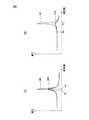
図1(a)は、SP方式において、送電側の共振回路の共振周波数よりも受電側の共振回路の共振周波数が大きいときの、受電側の共振回路の出力電圧の周波数特性の一例を示す図である。また図1(b)は、SP方式において、送電側の共振回路の共振周波数と受電側の共振回路の共振周波数とが略等しいときの、受電側の共振回路の出力電圧の周波数特性の一例を示す図である。図1(a)及び図1(b)において、横軸は周波数を表し、縦軸は電圧を表す。そして図1(a)に示されるグラフ101は、送電側の共振回路の共振周波数よりも受電側の共振回路の共振周波数が大きいときの、受電側の共振回路の出力電圧の周波数特性を表す。また、図1(b)に示されるグラフ102は、送電側の共振回路の共振周波数と受電側の共振回路の共振周波数とが略等しいときの、受電側の共振回路の出力電圧の周波数特性を表す。グラフ101に示されるように、送電側の共振回路の共振周波数よりも受電側の共振回路の共振周波数が大きい場合、送電側の共振回路の共振周波数f1、または、受電側の共振回路の共振周波数f2において、出力電圧がピークとなる。一方、グラフ102に示されるように、送電側の共振回路の共振周波数と受電側の共振回路の共振周波数とが略等しい場合には、送電側と受電側とで共通する共振周波数f3において出力電圧がピークとなる。そしてそのピーク電圧は、送電側の共振回路の共振周波数よりも受電側の共振回路の共振周波数が大きい場合における、何れの電圧のピークよりも高くなる。 FIG. 1A is a diagram illustrating an example of the frequency characteristic of the output voltage of the power receiving side resonance circuit when the resonance frequency of the power receiving side resonance circuit is larger than the resonance frequency of the power transmission side resonance circuit in the SP method. It is. FIG. 1B shows an example of the frequency characteristic of the output voltage of the power receiving side resonance circuit when the resonance frequency of the power transmitting side resonance circuit and the resonance frequency of the power receiving side resonance circuit are substantially equal in the SP method. FIG. 1A and 1B, the horizontal axis represents frequency, and the vertical axis represents voltage. A
図2(a)は、送電側及び受電側の共振回路を図1(a)と同じ共振回路としたときの、送電側の共振回路の送信コイルに流れる電流の周波数特性を表す。また図2(b)は、送電側及び受電側の共振回路を図1(b)と同じ共振回路としたときの、送電側の共振回路の送信コイルに流れる電流の周波数特性を表す。図2(a)及び図2(b)において、横軸は周波数を表し、縦軸は電流を表す。そして図2(a)に示されるグラフ201は、図1(a)に示される受電側の共振回路の出力電圧の周波数特性に対応する、送信コイルに流れる電流の周波数特性を表す。また、図2(b)に示されるグラフ202は、図1(b)に示される受電側の共振回路の出力電圧の周波数特性に対応する、送信コイルに流れる電流の周波数特性を表す。グラフ201及びグラフ202に示されように、受電側の共振回路の出力電圧が同じでも、送電側の共振回路の共振周波数と受電側の共振回路の共振周波数とが略等しい場合の方が、送信コイルに流れる電流は大きくなる。例えば、グラフ101及びグラフ102に示されるように、送電側の共振回路の共振周波数よりも受電側の共振回路の共振周波数が大きい場合における、受電側の共振周波数f2での出力電圧と、送電側の共振回路の共振周波数と受電側の共振回路の共振周波数とが略等しい場合における、周波数f4での出力電圧とが略等しくなる。これに対して、グラフ201及びグラフ202に示されるように、送電側の共振回路の共振周波数よりも受電側の共振回路の共振周波数が大きい場合における、共振周波数f2での送信コイルに流れる電流値I1よりも、送電側の共振回路の共振周波数と受電側の共振回路の共振周波数とが略等しい場合における、周波数f4での送信コイルに流れる電流値I2の方が大きい。このことから、送電側の共振回路の共振周波数と受電側の共振回路の共振周波数とを等しくするよりも、送電側の共振回路の共振周波数間の受電側の共振回路の共振周波数の差を大きくして、送電側の共振回路が共振しないような周波数を持つ交流電力を用いた方が、エネルギー伝送効率が高くなることが分かる。これは、送電側の共振回路の共振周波数と受電側の共振回路の共振周波数とが等しい場合、送信コイルと受信コイル間の結合度が低くなるほど、送信コイルと受信コイル間の相互インダクタンスが小さくなり、その結果として、負荷とは無関係に送信コイルに流れる電流が増加するためである。 FIG. 2A illustrates the frequency characteristics of the current flowing through the transmission coil of the power transmission side resonance circuit when the power transmission side and power reception side resonance circuits are the same as those in FIG. FIG. 2B shows frequency characteristics of the current flowing through the transmission coil of the power transmission side resonance circuit when the power transmission side and power reception side resonance circuits are the same as those in FIG. 2A and 2B, the horizontal axis represents frequency, and the vertical axis represents current. A
そこでこの非接触給電装置では、送電側に共振回路を設けず、受電側において受電コイルと並列に接続され、受電コイルとともに共振回路を構成する可変容量回路の静電容量を、受電側の共振回路の出力電圧に応じて制御することで、送信コイルに流れる電流を抑制するとともに、共振回路に流れる循環電流を抑制する。これにより、この非接触給電装置は、送信コイルと受信コイル間の結合度が動的に変化しても、エネルギー伝送効率が低下することを抑制する。 Therefore, in this non-contact power feeding device, the resonance circuit on the power receiving side is not provided, and the capacitance of the variable capacitance circuit that is connected in parallel with the power receiving coil on the power receiving side and forms the resonance circuit together with the power receiving coil is changed to the resonance circuit on the power receiving side. By controlling according to the output voltage, the current flowing through the transmission coil is suppressed, and the circulating current flowing through the resonance circuit is suppressed. Thereby, this non-contact electric power supply suppresses that energy transmission efficiency falls even if the coupling degree between a transmission coil and a receiving coil changes dynamically.
なお、本明細書で開示されるように、1次側(送信側)にて共振回路を利用せず、2次側(受電側)に、送信コイルを短絡した際の受信コイルのインダクタンスと、受信コイルに並列に接続される容量素子の静電容量とに応じた共振周波数を持つ共振回路を設ける非接触給電方式を、以下では、2次側共振(second resonance)方式と呼ぶ。なお、1次側にて、送信コイルと直列または並列に接続される容量素子が存在する場合でも、その容量素子と送信コイルによる共振周波数が、送信コイルに供給される交流電力にて1次側が共振しない程度に2次側の共振周波数よりも低い場合の非接触給電方式も、second resonance方式に含まれるものとする。また、second resonance方式において、送信コイルを短絡した際の受信コイルのインダクタンスと、受信コイルに並列に接続される容量素子の静電容量とに応じた共振周波数をsecond resonance周波数と呼ぶ。 As disclosed in this specification, the inductance of the reception coil when the transmission coil is short-circuited on the secondary side (power reception side) without using the resonance circuit on the primary side (transmission side); A non-contact power feeding method in which a resonance circuit having a resonance frequency corresponding to the capacitance of a capacitive element connected in parallel to the receiving coil is referred to as a secondary resonance method. Even when there is a capacitive element connected in series or in parallel with the transmission coil on the primary side, the resonance frequency of the capacitive element and the transmission coil is such that the primary side is the AC power supplied to the transmission coil. The non-contact power feeding method in the case where the resonance frequency is lower than the resonance frequency on the secondary side so as not to resonate is also included in the second resonance method. In the second resonance method, a resonance frequency corresponding to the inductance of the receiving coil when the transmitting coil is short-circuited and the capacitance of the capacitive element connected in parallel to the receiving coil is called a second resonance frequency.
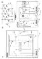
図3(a)は、本発明の一つの実施形態に係る非接触給電装置の概略構成図である。また図3(b)は、可変容量回路の回路図である。図3(a)に示されるように、非接触給電装置1は、送電装置2と、送電装置2から空間を介して給電される受電装置3とを有する。送電装置2は、電力供給回路10と、送信コイル13と、ゲートドライバ14と、制御回路15とを有する。一方、受電装置3は、受信コイル21及び可変容量回路22を有する共振回路20と、整流平滑回路23と、負荷回路24と、電圧検出回路25と、制御回路26とを有する。 FIG. 3A is a schematic configuration diagram of a non-contact power feeding device according to one embodiment of the present invention. FIG. 3B is a circuit diagram of the variable capacitance circuit. As illustrated in FIG. 3A, the non-contact power feeding device 1 includes a
先ず、送電装置2について説明する。
電力供給回路10は、所定のスイッチング周波数を持つ交流電力を送信コイル13へ供給する。そのために、電力供給回路10は、直流電源11と、4個のスイッチング素子12−1〜12−4とを有する。First, the
The
直流電源11は、所定の電圧を持つ直流電力を供給する。そのために、直流電源11は、例えば、バッテリを有していてもよい。あるいは、直流電源11は、商用の交流電源と接続され、その交流電源から供給された交流電力を直流電力に変換するための全波整流回路及び平滑コンデンサを有していてもよい。 The
4個のスイッチング素子12−1〜12−4は、例えば、nチャネル型のMOSFETとすることができる。そして4個のスイッチング素子12−1〜12−4のうち、スイッチング素子12−1とスイッチング素子12−2は、直流電源11の正極側端子と負極側端子との間に直列に接続される。また本実施形態では、直流電源11の正極側に、スイッチング素子12−1が接続され、一方、直流電源11の負極側に、スイッチング素子12−2が接続される。そしてスイッチング素子12−1のドレイン端子は、直流電源11の正極側端子と接続され、スイッチング素子12−1のソース端子は、スイッチング素子12−2のドレイン端子と接続される。また、スイッチング素子12−2のソース端子は、直流電源11の負極側端子と接続される。さらに、スイッチング素子12−1のソース端子、及び、スイッチング素子12−2のドレイン端子は、送信コイル13の一端に接続され、スイッチング素子12−2のソース端子は、スイッチング素子12−4を介して送信コイル13の他端に接続される。 The four switching elements 12-1 to 12-4 can be, for example, n-channel MOSFETs. Of the four switching elements 12-1 to 12-4, the switching element 12-1 and the switching element 12-2 are connected in series between the positive terminal and the negative terminal of the
同様に、4個のスイッチング素子12−1〜12−4のうち、スイッチング素子12−3とスイッチング素子12−4は、スイッチング素子12−1及びスイッチング素子12−2と並列に、かつ、直流電源11の正極側端子と負極側端子との間に直列に接続される。また、直流電源11の正極側に、スイッチング素子12−3が接続され、一方、直流電源11の負極側に、スイッチング素子12−4が接続される。そしてスイッチング素子12−3のドレイン端子は、直流電源11の正極側端子と接続され、スイッチング素子12−3のソース端子は、スイッチング素子12−4のドレイン端子と接続される。また、スイッチング素子12−4のソース端子は、直流電源11の負極側端子と接続される。さらに、スイッチング素子12−3のソース端子、及び、スイッチング素子12−4のドレイン端子は、送信コイル13の他端に接続される。 Similarly, among the four switching elements 12-1 to 12-4, the switching element 12-3 and the switching element 12-4 are parallel to the switching element 12-1 and the switching element 12-2 and are connected to the DC power source. 11 are connected in series between the positive terminal and the negative terminal. Further, the switching element 12-3 is connected to the positive electrode side of the
また、各スイッチング素子12−1〜12−4のゲート端子は、ゲートドライバ14を介して制御回路15と接続される。さらに、各スイッチング素子12−1〜12−4のゲート端子は、オンとなる電圧が印加されたときにそのスイッチング素子がオンとなることを保証するために、それぞれ、抵抗を介して自素子のソース端子と接続されてもよい。そして各スイッチング素子12−1〜12−4は、制御回路15からの制御信号にしたがって、所定のスイッチング周波数にてオン/オフが切り替えられる。本実施形態では、スイッチング素子12−1とスイッチング素子12−4とがオンとなっている間、スイッチング素子12−2とスイッチング素子12−3とがオフとなり、逆に、スイッチング素子12−2とスイッチング素子12−3とがオンとなっている間、スイッチング素子12−1とスイッチング素子12−4とがオフとなるように、スイッチング素子12−1とスイッチング素子12−4の組と、スイッチング素子12−2とスイッチング素子12−3との組について交互にオン/オフが切り替えられる。これにより、直流電源11から供給された直流電力は、各スイッチング素子のスイッチング周波数を持つ交流電力に変換されて、送信コイル13に供給される。 The gate terminals of the switching elements 12-1 to 12-4 are connected to the
そして送信コイル13は、電力供給回路10から供給された交流電力を、空間を介して受電装置3の共振回路20へ伝送する。 Then, the
ゲートドライバ14は、制御回路15から、各スイッチング素子12−1〜12−4のオン/オフを切り替える制御信号を受信し、その制御信号に応じて、各スイッチング素子12−1〜12−4のゲート端子に印加する電圧を変化させる。すなわち、ゲートドライバ14は、スイッチング素子12−1及びスイッチング素子12−4をオンにする制御信号を受け取ると、スイッチング素子12−1のゲート端子及びスイッチング素子12−4のゲート端子に、スイッチング素子12−1及びスイッチング素子12−4がオンとなる相対的に高い電圧を印加する。これにより、直流電源11からの電流が、スイッチング素子12−1、送信コイル13及びスイッチング素子12−4を介して流れるようになる。一方、ゲートドライバ14は、スイッチング素子12−1及びスイッチング素子12−4をオフにする制御信号を受け取ると、スイッチング素子12−1のゲート端子及びスイッチング素子12−4のゲート端子に、スイッチング素子12−1及びスイッチング素子12−4がオフとなり、直流電源11からの電流がスイッチング素子12−1及びスイッチング素子12−4を流れなくなる、相対的に低い電圧を印加する。ゲートドライバ14は、スイッチング素子12−2及びスイッチング素子12−3についても同様に、ゲート端子に印加する電圧を制御する。したがって、スイッチング素子12−1及びスイッチング素子12−4がオフとなり、スイッチング素子12−2及びスイッチング素子12−3がオンとなると、直流電源11からの電流が、スイッチング素子12−3、送信コイル13及びスイッチング素子12−2を介して流れるようになる。 The
制御回路15は、例えば、不揮発性のメモリ回路及び揮発性のメモリ回路と、演算回路と、他の回路と接続するためのインターフェース回路とを有する。そして制御回路15は、電力供給回路10が送信コイル13に交流電力を供給できるよう、電力供給回路10の各スイッチング素子のオンとオフとの切り替えを制御する。 The
本実施形態では、制御回路15は、スイッチング素子12−1及びスイッチング素子12−4の組とスイッチング素子12−2及びスイッチング素子12−3の組とが交互にオンとなり、かつ、スイッチング周波数に対応する1周期内でスイッチング素子12−1及びスイッチング素子12−4の組がオンとなっている期間とスイッチング素子12−2及びスイッチング素子12−3の組がオンとなっている期間とが等しくなるように、各スイッチング素子12−1〜12−4を制御する。なお、制御回路15は、スイッチング素子12−1及びスイッチング素子12−4の組とスイッチング素子12−2及びスイッチング素子12−3の組が同時にオンとなり、直流電源11が短絡されることを防止するために、スイッチング素子12−1及びスイッチング素子12−4の組とスイッチング素子12−2及びスイッチング素子12−3の組のオン/オフを切り替える際に、両方のスイッチング素子の組がオフとなるデッドタイムを設けてもよい。 In the present embodiment, the
次に、受電装置3について説明する。
共振回路20は、互いに並列に接続される受信コイル21と可変容量回路22とからなるLC共振回路である。そして共振回路20が有する受信コイル21の一端が可変容量回路22の一端に接続されるとともに、整流平滑回路23の一方の入力端子に接続される。また、受信コイル21の他端が可変容量回路22の他端に接続されるとともに、整流平滑回路23の他方の入力端子に接続される。Next, the
The
受信コイル21は、送電装置2の送信コイル13に流れる交流電流と共振することで、送信コイル13から電力を受信する。そして受信コイル21は、可変容量回路22を介して受信した電力を整流平滑回路23へ出力する。なお、受信コイル21の巻き数と、送電装置2の送信コイル13の巻き数は同一でもよく、あるいは、異なっていてもよい。また、共振回路20の受信コイル21のインダクタンス及び可変容量回路22の静電容量が取り得る範囲は、想定される結合度(例えば、k=0.1〜0.5)において共振周波数(second resonance 周波数)fr2=100kHzとなるように設定されればよい。The
可変容量回路22は、静電容量を調節可能な回路であり、その一端で受信コイル21の一端及び整流平滑回路23の一方の入力端子と接続され、他端で受信コイル21の他端及び整流平滑回路23の他方の入力端子と接続される。すなわち、可変容量回路22は、受信コイル21と並列に接続される。そして可変容量回路22は、受信コイル21とともに共振して、受信コイル21にて受信した電力を、整流平滑回路23へ出力する。 The
本実施形態では、可変容量回路22は、受信コイル21とそれぞれ並列に接続される、3個のコンデンサ221〜223と、3個のスイッチング素子224〜226とを有する。そしてコンデンサ221とスイッチング素子224とは直列に接続される。同様に、コンデンサ222とスイッチング素子225とが直列に接続され、コンデンサ223とスイッチング素子226とが直列に接続される。なお、可変容量回路22が有する、受信コイル21と並列に接続されるコンデンサの数は3個に限られない。可変容量回路22が有する、受信コイル21と並列に接続されるコンデンサの数は複数であればよく、例えば、2個あるいは4個以上であってもよい。 In the present embodiment, the
スイッチング素子224〜226は、例えば、nチャネル型のMOSFETとすることができる。そしてスイッチング素子224のドレイン端子は、コンデンサ221を介して受信コイル21の一端と接続され、スイッチング素子224のソース端子は、受信コイル21の他端と接続される。同様に、スイッチング素子225のドレイン端子は、コンデンサ222を介して受信コイル21の一端と接続され、スイッチング素子225のソース端子は、受信コイル21の他端と接続され、スイッチング素子226のドレイン端子は、コンデンサ223を介して受信コイル21の一端と接続され、スイッチング素子226のソース端子は、受信コイル21の他端と接続される。また、各スイッチング素子224〜226のゲート端子は、制御回路26と接続される。 The switching
スイッチング素子224〜226は、それぞれ、制御回路26により、オン/オフが切り替えられる。そしてコンデンサ221〜223のうち、オンとなったスイッチング素子と直列に接続されるコンデンサが共振回路20の共振に寄与する。すなわち、共振回路20の共振周波数(second resonance 周波数)fr2は、次式で表される。
(1)式から明らかなように、コンデンサ221〜223のうち、共振回路20の共振に寄与するコンデンサが増えるほど、すなわち、オンとなるスイッチング素子が増えるほど、可変容量回路22の静電容量は増加するので、共振回路20の共振周波数fr2は低下する。逆に、コンデンサ221〜223のうち、共振回路20の共振に寄与しないコンデンサが増えるほど、すなわち、オフとなるスイッチング素子が増えるほど、共振回路20の共振周波数fr2は高くなる。As apparent from the equation (1), the capacitance of the
整流平滑回路23は、ブリッジ接続された4個のダイオードを有する全波整流回路231と平滑コンデンサ232とを有し、共振回路20により受信された電力を整流し、かつ、平滑化して、直流電力に変換する。そして整流平滑回路23は、その直流電力を、負荷回路24に出力する。 The rectifying / smoothing
電圧検出回路25は、全波整流回路231の両端子間の出力電圧を検出する。全波整流回路231の両端子間の出力電圧は、共振回路20の出力電圧と1対1に対応するので、全波整流回路231の両端子間の出力電圧を検出することは、間接的に共振回路20の出力電圧を検出することとなる。電圧検出回路25は、例えば、直流電圧を検出できる公知の様々な電圧検出回路の何れかとすることができる。なお、本実施形態では、電圧検出回路25は、出力電圧が可変容量回路22の各スイッチング素子のオンとオフとを切り替えるための閾値電圧よりも高いか否かを検出できればよいので、そのような検出を行うことが可能な回路であればよい。 The
制御回路26は、電圧検出回路25による電圧検出結果に応じて、共振回路20の可変容量回路22の静電容量を制御する。 The
図4(a)は、second resonance方式による、共振回路20の出力電圧の周波数特性の一例を示す図である。図4(a)において、横軸は周波数を表し、縦軸は電圧を表す。グラフ400は、共振回路20の共振周波数がfr2であり、かつ、負荷回路24がある負荷抵抗を持つ場合の出力電圧の周波数特性を表し、グラフ401は、共振回路20の共振周波数がfr2であり、かつ、負荷回路24の負荷抵抗が、グラフ400に関する負荷抵抗の100倍の値を持つ場合の出力電圧の周波数特性を表す。グラフ400及びグラフ401で示されるように、送信コイル13に供給される交流電力のスイッチング周波数が共振回路20の共振周波数fr2に近づくほど、出力電圧は高くなる。また、共振周波数fr2近傍では、second resonance方式の非接触給電装置は定電流駆動となるため、負荷回路24の負荷抵抗に応じて出力電圧が大きく変化する。FIG. 4A is a diagram illustrating an example of frequency characteristics of the output voltage of the
一方、送信コイル13に供給される交流電力のスイッチング周波数が共振回路の共振周波数fr2から離れると、非接触給電装置は定電圧駆動となり、負荷回路24の負荷抵抗が変化しても、出力電圧はほぼ一定となる。On the other hand, when the switching frequency of the AC power supplied to the
そこで、例えば、結合度が変化することにより、共振回路20の共振周波数fr2が送信コイル13に供給される交流電力のスイッチング周波数と近づいて、共振回路20の出力電圧が高くなると、制御回路26は、共振回路20の共振周波数fr2を変化させて、スイッチング周波数と共振周波数fr2の差を大きくすることで、受電装置3に定電圧駆動を継続させることができる。Therefore, for example, when the coupling frequency changes so that the resonance frequencyfr2 of the
図4(b)は、共振回路20の共振周波数をfr2からfr2'に変化させたときの出力電圧の周波数特性の一例を示す図である。図4(b)において、横軸は周波数を表し、縦軸は電圧を表す。グラフ410は、共振回路20の共振周波数がfr2'であり、かつ、負荷回路24がある負荷抵抗を持つ場合の出力電圧の周波数特性を表し、グラフ411は、共振回路20の共振周波数がfr2'であり、かつ、負荷回路24の負荷抵抗が、グラフ410に関する負荷抵抗の100倍の値を持つ場合の出力電圧の周波数特性を表す。4 (b) is a diagram showing an example of a frequency characteristic of the output voltage when the resonant frequency of the
例えば、図4(a)に示されるように、送信コイル13に供給される交流電力のスイッチング周波数fsが共振回路20の共振周波数fr2に近い場合、出力電圧は上昇する。そこで、出力電圧の上昇を検知して、図4(b)に示されるように、共振回路20の共振周波数をfr2からfr2'に変化させることで、共振周波数をfr2'がスイッチング周波数fsに対して十分に高くなるので、送信コイル13に供給される交流電力のスイッチング周波数fsが一定に保たれたままでも、定電圧駆動が維持される。For example, as shown in FIG. 4 (a), when the switching frequency fs of the AC power supplied to the
したがって、制御回路26は、共振回路20の出力電圧が上昇すると、可変容量回路22の静電容量を低下させるよう、可変容量回路22の静電容量を制御する。本実施形態では、制御回路26は、共振回路20の出力電圧が上昇するほど、スイッチング素子224〜226のうち、オフにするスイッチング素子の数を増やす。これにより、(1)式に示されるように、共振回路20の共振周波数fr2が高くなり、その結果として、制御回路26は、送信コイル13に供給される交流電力のスイッチング周波数fsと共振回路20の共振周波数fr2の差を大きくすることができるので、受電装置3の定電圧駆動を維持することができる。また、これにより、共振回路20に流れる循環電流が増大することが抑制され、電力伝送効率の低下が抑制されるとともに、受電装置3において過電圧が生じることが防止される。Therefore, the
逆に、共振回路20の出力電圧が低下すると、制御回路26は、可変容量回路22の静電容量を上昇させるよう、可変容量回路22の静電容量を制御する。本実施形態では、制御回路26は、共振回路20の出力電圧が低下するほど、スイッチング素子224〜226のうち、オンにするスイッチング素子の数を増やせばよい。 Conversely, when the output voltage of the
なお、制御回路26は、共振回路20の出力電圧の上昇が検知された場合に、共振回路20の共振周波数を低下させるように可変容量回路22の静電容量を制御して、共振回路20の共振周波数fr2を、送信コイル13に供給される交流電力のスイッチング周波数fsよりも低くしてもよい。制御回路26は、このように可変容量回路22の静電容量を制御しても、受電装置3において過電圧が生じることを防止できる。ただしこの場合には、共振回路20のQ値が大きくなり、その結果として、共振回路20に流れる電流も増大する。The
また、結合度と、下記の(2)式で表される受信コイル21のQ値との積(以下、kQ積と呼ぶ)が大きくなるほど、送信コイル13を流れる電流の位相が相対的に進む。
図5は、受電装置3の電圧検出回路25及び制御回路26の一例を示す図である。図5に示されるように、制御回路26は、整流回路261と、分圧回路262と、スイッチング回路263とを有する。なお、図5では、説明の簡単化のために、電圧検出回路25及び制御回路26のスイッチング回路263に関して、可変容量回路22が有する複数のスイッチング素子のうちの一つ(スイッチング素子224)のオン/オフを切り替えるための回路が示されている。電圧検出回路25及び制御回路26のスイッチング回路263は、可変容量回路22のスイッチング素子ごとに、図5に示された回路を有していればよい。 FIG. 5 is a diagram illustrating an example of the
この例では、電圧検出回路25は、全波整流回路231の正極側出力端子と負極側出力端子間に直列に接続されるツェナーダイオードZD1と、二つの抵抗Rvm1、Rvm2とを有する。ツェナーダイオードZD1は、全波整流回路231から出力される電圧にて逆バイアスされるよう、カソード端子が全波整流回路231の正極側出力端子と接続され、アノード端子が二つの抵抗Rvm1、Rvm2を介して全波整流回路231の負極側出力端子と接続される。 In this example, the
したがって、全波整流回路231から出力される電圧がツェナーダイオードZD1の降伏電圧以下である場合には、電圧検出回路25に電流は流れず、一方、全波整流回路231から出力される電圧がツェナーダイオードZD1の降伏電圧よりも高くなると、電圧検出回路25に電流が流れるようになる。したがって、電圧検出回路25は、全波整流回路231から出力される電圧がツェナーダイオードZD1の降伏電圧よりも高いか否かを検知することができる。すなわち、ツェナーダイオードZD1の降伏電圧が、可変容量回路22の対応するスイッチング素子のオン/オフを切り替えるための閾値電圧となる。 Therefore, when the voltage output from the full-
なお、可変容量回路22のスイッチング素子ごとに、対応する電圧検出回路25のツェナーダイオードの降伏電圧も異なることが好ましい。これにより、電圧検出回路25は、可変容量回路22のスイッチング素子ごとに、スイッチング素子のオン/オフが切り替えられる電圧を互いに異ならせることができる。 Note that the breakdown voltage of the Zener diode of the corresponding
制御回路26の整流回路261は、共振回路20の受信コイル21に対して並列に接続され、ダイオードDとコンデンサCとを有する。ダイオードDのカソード端子とコンデンサCの一端とが接続されるように、ダイオードDとコンデンサCは直列に接続される。そして整流回路261は、受信コイル21が受電した交流電力を整流し、ダイオードDのカソード端子とコンデンサCの一端との間から整流された直流電圧を分圧回路262へ供給する。 The
分圧回路262は、整流回路261のコンデンサCの両端子間に直列に接続される二つの抵抗Rd1、Rd2と、抵抗Rd2と並列に接続されるツェナーダイオードZD2とを有する。そして分圧回路262は、整流回路261から供給された直流電圧を、抵抗Rd1と抵抗Rd2とで分圧し、抵抗Rd1と抵抗Rd2の間に接続された端子から、その分圧により得られた直流電圧をスイッチング素子224のゲート端子へ供給する。またツェナーダイオードZD2は、そのカソード端子が、抵抗Rd1と抵抗Rd2の間に接続された端子及びスイッチング素子224のゲート端子と接続され、アノード端子が抵抗R2の他端、及び、スイッチング素子224のソース端子と接続されるように設けられる。これにより、受信コイル21が一定以上の電力を受電しており、かつ、詳細は後述するように、スイッチング回路263がオフとなっている間、スイッチング素子224のゲート端子にツェナーダイオードZD2の降伏電圧に相当する電圧が印加されるようになる。
なお、可変容量回路22の他のスイッチング素子についても同様に、抵抗Rd1と抵抗Rd2の間に接続された端子から、そのスイッチング素子のゲート端子に直流電圧が供給されればよい。The
Similarly, for the other switching elements of the
スイッチング回路263は、抵抗Rと、フォトカプラPCと、npn型のトランジスタTrとを有する。そして全波整流回路231の正極側出力端子と負極側出力端子の間に、正極側から順に、抵抗Rと、フォトカプラPCの発光ダイオードと、トランジスタTrとが直列に接続される。すなわち、フォトカプラPCの発光ダイオードのアノード端子が抵抗Rを介して全波整流回路231の正極側出力端子と接続され、その発光ダイオードのカソード端子がトランジスタTrのコレクタ端子と接続され、トランジスタTrのエミッタ端子が全波整流回路231の負極側出力端子と接続される。またトランジスタTrのベース端子は、電圧検出回路25の抵抗Rvm1と抵抗Rvm2との間に接続される。一方、フォトカプラPCのフォトトランジスタの一端は、可変容量回路22のスイッチング素子224のゲート端子と接続され、フォトトランジスタの他端は、スイッチング素子224のソース端子と接続される。 The
全波整流回路231から出力される電圧が電圧検出回路25の閾値電圧以下、すなわち、ツェナーダイオードZD1の降伏電圧以下である場合、電圧検出回路25には電流が流れないので、スイッチング回路263のトランジスタTrのベース端子にも電流が流れず、トランジスタTrはオフとなる。そのため、フォトカプラPCもオフとなる。その結果、スイッチング素子224のゲート端子には、分圧回路262からの電圧により、スイッチング素子224はオンとなる。そのため、スイッチング素子224と直列に接続されるコンデンサ221は、共振回路20の共振に寄与する。 When the voltage output from the full-
一方、全波整流回路231から出力される電圧が電圧検出回路25の閾値電圧よりも高くなると、電圧検出回路25には電流が流れるようになり、スイッチング回路263のトランジスタTrのベース端子にも電流が流れて、トランジスタTrはオンとなる。そのため、フォトカプラPCもオンとなる。その結果、分圧回路262からスイッチング素子224のゲート端子に印加される電圧も低下し、スイッチング素子224はオフとなる。そのため、スイッチング素子224と直列に接続されるコンデンサ221は、共振回路20の共振に寄与しなくなる。 On the other hand, when the voltage output from the full-
このように、制御回路26は、電圧検出回路25により検出される、全波整流回路231から出力される電圧が閾値電圧よりも高くなると、可変容量回路22のコンデンサ221を、共振回路20の共振に寄与しないようにして、共振回路20の共振周波数fr2を高くすることができる。
制御回路26は、可変容量回路22の他のコンデンサについても、同様に、全波整流回路231から出力される電圧がそのコンデンサについての閾値電圧よりも高くなると、共振回路20の共振に寄与しないようにすることができる。Thus, when the voltage output from the full-
Similarly, the
以上に説明してきたように、この非接触給電装置は、送電装置の共振回路を設けないことで、結合度が低下する場合でも、送信コイルに流れる電流の増加を抑制する。また、この非接触給電装置は、受電装置の共振回路の出力電圧をモニタし、その出力電圧が上昇すると受電側の共振回路の可変容量回路の静電容量を変更して、その共振回路の共振周波数と送電装置の送信コイルに供給される交流電力のスイッチング周波数との差を大きくして、共振回路に流れる循環電流が増大することを抑制するとともに、受電装置に過電圧が印加されることを防止する。これにより、この非接触給電装置は、送信コイルと受信コイル間の結合度が動的に変化しても、エネルギー伝送効率の低下を抑制できる。さらに、過電圧が印加されることを防止することにより、この非接触給電装置は、受電装置が故障することを防止できる。 As described above, this non-contact power feeding device suppresses an increase in current flowing through the transmission coil even when the degree of coupling is reduced by not providing the resonance circuit of the power transmission device. In addition, this non-contact power supply device monitors the output voltage of the resonance circuit of the power receiving device, and when the output voltage rises, changes the capacitance of the variable capacitance circuit of the resonance circuit on the power receiving side, The difference between the frequency and the switching frequency of the AC power supplied to the transmission coil of the power transmission device is increased to prevent an increase in circulating current flowing through the resonance circuit and to prevent an overvoltage from being applied to the power reception device To do. Thereby, this non-contact electric power feeder can suppress the fall of energy transmission efficiency, even if the coupling degree between a transmission coil and a receiving coil changes dynamically. Further, by preventing the overvoltage from being applied, the non-contact power feeding device can prevent the power receiving device from being damaged.
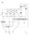
なお、変形例によれば、整流平滑回路23において、全波整流回路231の代わりに、半波整流回路が用いられ、電圧検出回路25は、半波整流回路からの出力電圧を検出することで、間接的に共振回路20の出力電圧を検出してもよい。 According to the modification, in the rectifying / smoothing
図6は、この変形例による、受電装置3の回路ブロック図である。この変形例において、受電装置3は、受信コイル21と可変容量回路22とを有する共振回路20と、整流平滑回路27と、負荷回路24と、電圧検出回路25と、制御回路26とを有する。
この変形例では、上記の実施形態による受電装置と比較して、整流平滑回路27が、全波整流回路の代わりに半波整流回路を有している点と、制御回路26のスイッチング回路263の構成が異なる。そこで以下では、その相違点について説明する。FIG. 6 is a circuit block diagram of the
In this modification, the rectifying / smoothing
この変形例では、整流平滑回路27は、直列に接続される二つのダイオードを有する半波整流回路271と、半波整流回路271と並列に接続される平滑コンデンサ272とを有する。そして共振回路20から出力される電力は、整流平滑回路27により半波整流される。 In this modification, the rectifying / smoothing
電圧検出回路25は、図5に示された電圧検出回路25と同様の回路とすることができ、整流平滑回路27の平滑コンデンサ272の正側の端子(すなわち、直列接続されるダイオードのカソード端子と接続される側の端子)とグラウンド間の電圧を検出する。そして検出された電圧が閾値電圧よりも高くなった場合に、制御回路26のスイッチング回路263のトランジスタ(図示せず)をオンにする。 The
制御回路26は、図5に示された整流回路261及び分圧回路262と同様の整流回路及び分圧回路を有する。そして制御回路26は、可変容量回路22の各スイッチング素子224〜226のゲート端子に、分圧回路により得られる電圧を印加する。また、制御回路26は、図5に示されたスイッチング回路263からフォトカプラPCを省略したスイッチング回路を有する。ただし、この変形例では、トランジスタのコレクタは、可変容量回路22の対応するスイッチング素子のゲート端子と接続され、トランジスタのエミッタは接地される。 The
この場合も、電圧検出回路25により検出された電圧が閾値電圧よりも高くなることで、トランジスタがオンになり、その結果として、可変容量回路22の対応するスイッチング素子のゲート端子に印加される電圧が低下して、そのスイッチング素子がオフとなる。そのため、そのスイッチング素子と直列に接続されるコンデンサが共振回路20の共振に寄与しなくなる。 Also in this case, when the voltage detected by the
この変形例では、受電装置3の各回路の基準電圧を共通の回路グラウンドとすることができるので、回路構成が簡単化される。 In this modification, since the reference voltage of each circuit of the
また他の変形例によれば、可変容量回路22が有する複数のコンデンサのうちの一つは、スイッチング素子を介さずに受信コイル21と並列に接続されてもよい。これにより、少なくとも一つのコンデンサが受信コイル21と常に並列に接続されるので、受電装置3は、常にsecond resonance方式に従って電力の受信を継続できる。 According to another modification, one of the plurality of capacitors included in the
さらに他の変形例によれば、可変容量回路22の構成は、上記の実施形態に限られず、例えば、可変容量回路22は機械式あるいは他の方式で静電容量を変化させることができる可変容量コンデンサを有していてもよい。そして可変容量回路22が機械式の可変容量コンデンサを有している場合には、制御回路26は、例えば、可変容量コンデンサの静電容量を調整するための機構を駆動するためのステッピングモータ及びステッピングモータを駆動するための回路などを有していてもよい。そして制御回路26は、電圧検出回路25により検出された電圧に応じた回転量だけステッピングモータを回転させることで、可変容量コンデンサの静電容量がその電圧に応じた静電容量となるように、可変容量回路22を制御してもよい。 According to still another modification, the configuration of the
さらに、送電装置2において、送信コイル13に交流電力を供給する電力供給回路は、上記の実施形態とは異なる回路構成を持っていてもよい。 Furthermore, in the
図7(a)〜図7(c)は、それぞれ、変形例による、電力供給回路の回路図である。図7(a)に示される電力供給回路110は、所定のスイッチング周波数を持つ交流電力を供給する交流電源111を有する。そして交流電源111からの交流電力が送信コイル13に直接供給される。したがって、この変形例では、制御回路15は省略されてもよい。 Fig.7 (a)-FIG.7 (c) are circuit diagrams of the electric power supply circuit by a modification, respectively. The
図7(b)に示される電力供給回路120は、直流電源11と、二つのスイッチング素子12−1及びスイッチング素子12−2と、送信コイル13と直列に接続される、直流遮断用のコンデンサ121とを有する。なお、この変形例においても、各スイッチング素子は、例えば、nチャネル型のMOSFETとすることができる。 The
この変形例では、スイッチング素子12−1とスイッチング素子12−2は、直流電源11の正極側端子と負極側端子との間に直列に接続される。また、直流電源11の正極側に、スイッチング素子12−1が接続され、一方、直流電源11の負極側に、スイッチング素子12−2が接続される。そしてスイッチング素子12−1のドレイン端子は、直流電源11の正極側端子と接続され、スイッチング素子12−1のソース端子は、スイッチング素子12−2のドレイン端子と接続される。また、スイッチング素子12−2のソース端子は、直流電源11の負極側端子と接続される。さらに、スイッチング素子12−1のソース端子、及び、スイッチング素子12−2のドレイン端子は、送信コイル13の一端に接続され、スイッチング素子12−2のソース端子は、コンデンサ121を介して送信コイル13の他端に接続される。また、各スイッチング素子のゲート端子は、ゲートドライバ14と接続される。 In this modification, the switching element 12-1 and the switching element 12-2 are connected in series between the positive electrode side terminal and the negative electrode side terminal of the
この変形例では、ゲートドライバ14が、制御回路15から制御信号に従って、スイッチング素子12−1とスイッチング素子12−2のオン/オフを交互に切り替えればよい。すなわち、スイッチング素子12−1がオンとなり、スイッチング素子12−2がオフとなる場合には、直流電源11からスイッチング素子12−1を介して送信コイル13へ電流が流れ、コンデンサ121が充電される。一方、スイッチング素子12−1がオフとなり、スイッチング素子12−2がオンとなる場合には、コンデンサ121が放電して、コンデンサ121から送信コイル13及びスイッチング素子12−2を介して電流が流れる。 In this modification, the
図7(c)に示される電力供給回路130も、電力供給回路120と同様に、直流電源11と、二つのスイッチング素子12−1及びスイッチング素子12−2と、送信コイル13と直列に接続されるコンデンサ121とを有する。ただし、電力供給回路130は、電力供給回路120と比較して、送信コイル13の一端が直流電源11の正極側端子と直接接続され、送信コイル13の他端がコンデンサ121を介してスイッチング素子12−1のソース端子、及び、スイッチング素子12−2のドレイン端子と接続される。 Similarly to the
この変形例でも、ゲートドライバ14が、制御回路15から制御信号に従って、スイッチング素子12−1とスイッチング素子12−2のオン/オフを交互に切り替えればよい。 Also in this modification, the
なお、図7(b)に示される電力供給回路120及び図7(c)に示される電力供給回路130について、スイッチング周波数にて送信コイル13とコンデンサ121とが共振回路として動作しないよう、送信コイル13とコンデンサ121の共振周波数が受電装置3の共振回路20の共振周波数の最小値及びスイッチング周波数よりも小さくなるように、コンデンサ121の静電容量が設定されることが好ましい。これにより、送信コイル13に流れる電流が増大して電力の伝送効率が低下することが抑制される。 For the
また、上記の実施形態において、電力供給回路120及び電力供給回路130と同様に、送信コイル13と直列に接続される、直流遮断用のコンデンサが設けられてもよい。ただしこの場合も、スイッチング周波数にて送信コイル13とコンデンサとが共振回路として動作しないよう、送信コイル13とコンデンサの共振周波数が受電装置3の共振回路20の共振周波数の最小値及びスイッチング周波数よりも小さくなるように、コンデンサの静電容量が設定されることが好ましい。 Further, in the above embodiment, a DC blocking capacitor connected in series with the
また、送信コイルに供給される交流電力のスイッチング周波数は一定でなくてもよく、例えば、送信コイルに流れる電流を電流計により測定し、送電装置の制御回路は、その電流値が所定の閾値以上となる場合にスイッチング周波数を低下させるよう制御してもよい。 Further, the switching frequency of the AC power supplied to the transmission coil may not be constant. For example, the current flowing through the transmission coil is measured by an ammeter, and the control circuit of the power transmission apparatus has a current value equal to or higher than a predetermined threshold value. In this case, the switching frequency may be controlled to be lowered.
このように、当業者は、本発明の範囲内で、実施される形態に合わせて様々な変更を行うことができる。 As described above, those skilled in the art can make various modifications in accordance with the embodiment to be implemented within the scope of the present invention.
1 非接触給電装置
2 送電装置
10、110、120、130 電力供給回路
11 直流電源
12−1〜12−4 スイッチング素子
13 送信コイル
14 ゲートドライバ
15 制御回路
3 受電装置
20 共振回路
21 受信コイル
22 可変容量回路
221〜223 コンデンサ
224〜226 スイッチング素子
23、27 整流平滑回路
231 全波整流回路
271 半波整流回路
232、272 平滑コンデンサ
24 負荷回路
25 電圧検出回路
26 制御回路
261 整流回路
262 分圧回路
263 スイッチング回路
111 交流電源
121 コンデンサDESCRIPTION OF SYMBOLS 1 Non-contact
Claims (4)
Translated fromJapanese前記送電装置は、
前記受電装置へ電力を供給する送信コイルと、
前記送信コイルに対して、前記送信コイルが共振しない周波数を持つ交流電力を供給する電力供給回路と、
を有し、
前記受電装置は、
前記送電装置からの電力を受信する受信コイルと、前記受信コイルと並列に接続される可変容量回路とを有し、前記受信コイルのインダクタンスと前記可変容量回路の静電容量に応じた周波数で共振する共振回路と、
前記共振回路からの出力電圧を検出する電圧検出回路と、
前記出力電圧に応じて前記可変容量回路の静電容量を制御する制御回路と、
を有する非接触給電装置。A non-contact power feeding device having a power transmission device and a power receiving device that transmits power in a non-contact manner from the power transmission device,
The power transmission device is:
A transmission coil for supplying power to the power receiving device;
A power supply circuit for supplying AC powerhaving a frequency at which the transmission coil does not resonate to the transmission coil ;
Have
The power receiving device is:
A receiving coil for receiving power from the power transmission device; and a variable capacitance circuit connected in parallel with the receiving coil, and resonating at a frequency corresponding to the inductance of the receiving coil and the capacitance of the variable capacitance circuit A resonant circuit to
A voltage detection circuit for detecting an output voltage from the resonance circuit;
A control circuit for controlling the capacitance of the variable capacitance circuit according to the output voltage;
The non-contact electric power feeder which has.
前記制御回路は、前記出力電圧に応じて前記少なくとも一つのスイッチング素子のオンとオフとを切り替える、請求項1または2に記載の非接触給電装置。The variable capacity circuit includes a plurality ofcapacitors, and at least one switching element or to be connected in series of the plurality ofcapacitors, each of the plurality ofcapacitors are connected in parallel with the receiving coil ,
The non-contact power feeding device according to claim 1, wherein the control circuit switches on and off of the at least one switching element according to the output voltage.
前記制御回路は、The control circuit includes:
前記共振回路からの前記出力電圧に基づいて前記少なくとも一つのスイッチング素子がオンとなる第1の電圧を生成する分圧回路と、A voltage dividing circuit that generates a first voltage that turns on the at least one switching element based on the output voltage from the resonant circuit;
前記出力電圧が所定の閾値電圧以下の場合に前記分圧回路により生成される前記第1の電圧を前記少なくとも一つのスイッチング素子に印加し、一方、前記出力電圧が前記所定の閾値電圧よりも高い場合に前記分圧回路により生成される前記第1の電圧を前記少なくとも一つのスイッチング素子に印加させないスイッチング回路とを有する、請求項3に記載の非接触給電装置。Applying the first voltage generated by the voltage dividing circuit to the at least one switching element when the output voltage is equal to or lower than a predetermined threshold voltage, while the output voltage is higher than the predetermined threshold voltage The contactless power supply device according to claim 3, further comprising a switching circuit that prevents the first voltage generated by the voltage dividing circuit from being applied to the at least one switching element.
Priority Applications (6)
| Application Number | Priority Date | Filing Date | Title |
|---|---|---|---|
| JP2017039682AJP6350699B1 (en) | 2017-03-02 | 2017-03-02 | Non-contact power feeding device |
| DE112017007157.7TDE112017007157T5 (en) | 2017-03-02 | 2017-11-24 | CONTACTLESS POWER SUPPLY |
| PCT/JP2017/042284WO2018159031A1 (en) | 2017-03-02 | 2017-11-24 | Noncontact power supply apparatus |
| KR1020197015687AKR20190074305A (en) | 2017-03-02 | 2017-11-24 | Contactless feeder |
| US16/468,179US10944293B2 (en) | 2017-03-02 | 2017-11-24 | Noncontact power supply apparatus |
| CN201780074093.4ACN110326187A (en) | 2017-03-02 | 2017-11-24 | Contactless power supply device |
Applications Claiming Priority (1)
| Application Number | Priority Date | Filing Date | Title |
|---|---|---|---|
| JP2017039682AJP6350699B1 (en) | 2017-03-02 | 2017-03-02 | Non-contact power feeding device |
Publications (2)
| Publication Number | Publication Date |
|---|---|
| JP6350699B1true JP6350699B1 (en) | 2018-07-04 |
| JP2018148640A JP2018148640A (en) | 2018-09-20 |
Family
ID=62779793
Family Applications (1)
| Application Number | Title | Priority Date | Filing Date |
|---|---|---|---|
| JP2017039682AActiveJP6350699B1 (en) | 2017-03-02 | 2017-03-02 | Non-contact power feeding device |
Country Status (6)
| Country | Link |
|---|---|
| US (1) | US10944293B2 (en) |
| JP (1) | JP6350699B1 (en) |
| KR (1) | KR20190074305A (en) |
| CN (1) | CN110326187A (en) |
| DE (1) | DE112017007157T5 (en) |
| WO (1) | WO2018159031A1 (en) |
Families Citing this family (9)
| Publication number | Priority date | Publication date | Assignee | Title |
|---|---|---|---|---|
| DE102016209871A1 (en) | 2016-06-06 | 2017-12-07 | Robert Bosch Gmbh | Punching device and method for punching a lumen and implanting an implant device |
| US11641134B2 (en)* | 2017-04-14 | 2023-05-02 | General Electric Company | Wireless charging device and a method for detecting a receiver device |
| DE102018206714A1 (en)* | 2018-05-02 | 2019-11-07 | Kardion Gmbh | Receiving unit and energy transmission system for wireless energy transmission |
| DE102018206754A1 (en) | 2018-05-02 | 2019-11-07 | Kardion Gmbh | Method and device for determining the temperature at a surface and use of the method |
| DE102018206750A1 (en) | 2018-05-02 | 2019-11-07 | Kardion Gmbh | Device for inductive energy transfer into a human body and its use |
| DE102018206731A1 (en) | 2018-05-02 | 2019-11-07 | Kardion Gmbh | Device for inductive energy transmission in a human body and use of the device |
| DE102018208555A1 (en) | 2018-05-30 | 2019-12-05 | Kardion Gmbh | Apparatus for anchoring a cardiac assist system in a blood vessel, method of operation, and method of making a device and cardiac assist system |
| JP7439385B2 (en)* | 2019-03-22 | 2024-02-28 | オムロン株式会社 | Contactless power supply device |
| US11699551B2 (en) | 2020-11-05 | 2023-07-11 | Kardion Gmbh | Device for inductive energy transmission in a human body and use of the device |
Family Cites Families (14)
| Publication number | Priority date | Publication date | Assignee | Title |
|---|---|---|---|---|
| JP2001160122A (en)* | 1999-12-02 | 2001-06-12 | Hitachi Ltd | Non-contact IC card |
| JP2002027744A (en)* | 2000-07-07 | 2002-01-25 | Sony Corp | Switching power supply |
| JP2002153060A (en)* | 2000-11-14 | 2002-05-24 | Sony Corp | Switching power circuit |
| JP2002262567A (en)* | 2001-03-05 | 2002-09-13 | Sony Corp | Switching power circuit |
| JP2004072832A (en)* | 2002-08-02 | 2004-03-04 | Hitachi Kiden Kogyo Ltd | Non-contact power feeding method |
| JP2006074848A (en)* | 2004-08-31 | 2006-03-16 | Hokushin Denki Kk | Non-contact power transmission system |
| US20120146424A1 (en) | 2010-12-14 | 2012-06-14 | Takashi Urano | Wireless power feeder and wireless power transmission system |
| NZ593946A (en)* | 2011-07-07 | 2014-05-30 | Powerbyproxi Ltd | An inductively coupled power transfer receiver |
| EP2824799B1 (en)* | 2012-03-06 | 2022-01-05 | Murata Manufacturing Co., Ltd. | Power transmission system |
| US9755534B2 (en)* | 2013-02-14 | 2017-09-05 | Nuvolta Technologies, Inc. | High efficiency high frequency resonant power conversion |
| JP6110236B2 (en)* | 2013-07-02 | 2017-04-05 | ルネサスエレクトロニクス株式会社 | Power receiving device and non-contact power feeding system |
| WO2015083550A1 (en)* | 2013-12-05 | 2015-06-11 | 株式会社村田製作所 | Power receiving device and power transmission system |
| JP6417992B2 (en) | 2015-02-06 | 2018-11-07 | 株式会社Ihi | Contactless power supply system |
| CN205725178U (en)* | 2016-06-28 | 2016-11-23 | 中惠创智无线供电技术有限公司 | A kind of circuit for controlling output voltage |
- 2017
- 2017-03-02JPJP2017039682Apatent/JP6350699B1/enactiveActive
- 2017-11-24KRKR1020197015687Apatent/KR20190074305A/ennot_activeCeased
- 2017-11-24CNCN201780074093.4Apatent/CN110326187A/enactivePending
- 2017-11-24DEDE112017007157.7Tpatent/DE112017007157T5/enactivePending
- 2017-11-24USUS16/468,179patent/US10944293B2/enactiveActive
- 2017-11-24WOPCT/JP2017/042284patent/WO2018159031A1/ennot_activeCeased
Also Published As
| Publication number | Publication date |
|---|---|
| CN110326187A (en) | 2019-10-11 |
| JP2018148640A (en) | 2018-09-20 |
| DE112017007157T5 (en) | 2019-11-28 |
| US10944293B2 (en) | 2021-03-09 |
| KR20190074305A (en) | 2019-06-27 |
| US20200014244A1 (en) | 2020-01-09 |
| WO2018159031A1 (en) | 2018-09-07 |
Similar Documents
| Publication | Publication Date | Title |
|---|---|---|
| JP6350699B1 (en) | Non-contact power feeding device | |
| US10714979B2 (en) | Wireless power receiving terminal and wireless charging system | |
| US11626759B2 (en) | System and method for providing inductive power at multiple power levels | |
| JP6904280B2 (en) | Non-contact power supply device | |
| JP6680243B2 (en) | Non-contact power supply device | |
| CN110582922B (en) | Non-contact power supply device | |
| CN111712991B (en) | Non-contact power supply device | |
| JP5324009B2 (en) | Power receiving device and non-contact power transmission system using the same | |
| CN112448484A (en) | Non-contact power supply device | |
| JP2015202030A (en) | Non-contact power supply device and non-contact power supply system | |
| JP2017103860A (en) | Non-contact power supply device | |
| WO2018131261A1 (en) | Non-contact power supply device | |
| JP7003445B2 (en) | Contactless power supply | |
| KR102117869B1 (en) | Wireless power receiver having active rectifier | |
| CN111699610A (en) | Non-contact power supply device |
Legal Events
| Date | Code | Title | Description |
|---|---|---|---|
| TRDD | Decision of grant or rejection written | ||
| A01 | Written decision to grant a patent or to grant a registration (utility model) | Free format text:JAPANESE INTERMEDIATE CODE: A01 Effective date:20180508 | |
| A61 | First payment of annual fees (during grant procedure) | Free format text:JAPANESE INTERMEDIATE CODE: A61 Effective date:20180521 | |
| R150 | Certificate of patent or registration of utility model | Ref document number:6350699 Country of ref document:JP Free format text:JAPANESE INTERMEDIATE CODE: R150 | |
| R250 | Receipt of annual fees | Free format text:JAPANESE INTERMEDIATE CODE: R250 |